WO2016013410A1 - 固体撮像素子および電子機器 - Google Patents
固体撮像素子および電子機器 Download PDFInfo
- Publication number
- WO2016013410A1 WO2016013410A1 PCT/JP2015/069827 JP2015069827W WO2016013410A1 WO 2016013410 A1 WO2016013410 A1 WO 2016013410A1 JP 2015069827 W JP2015069827 W JP 2015069827W WO 2016013410 A1 WO2016013410 A1 WO 2016013410A1
- Authority
- WO
- WIPO (PCT)
- Prior art keywords
- photoelectric conversion
- solid
- layer
- state imaging
- imaging device
- Prior art date
- Legal status (The legal status is an assumption and is not a legal conclusion. Google has not performed a legal analysis and makes no representation as to the accuracy of the status listed.)
- Ceased
Links
Images






Classifications
-
- G—PHYSICS
- G02—OPTICS
- G02B—OPTICAL ELEMENTS, SYSTEMS OR APPARATUS
- G02B13/00—Optical objectives specially designed for the purposes specified below
- G02B13/001—Miniaturised objectives for electronic devices, e.g. portable telephones, webcams, PDAs, small digital cameras
- G02B13/0085—Miniaturised objectives for electronic devices, e.g. portable telephones, webcams, PDAs, small digital cameras employing wafer level optics
-
- G—PHYSICS
- G02—OPTICS
- G02B—OPTICAL ELEMENTS, SYSTEMS OR APPARATUS
- G02B7/00—Mountings, adjusting means, or light-tight connections, for optical elements
- G02B7/28—Systems for automatic generation of focusing signals
- G02B7/34—Systems for automatic generation of focusing signals using different areas in a pupil plane
-
- G—PHYSICS
- G02—OPTICS
- G02B—OPTICAL ELEMENTS, SYSTEMS OR APPARATUS
- G02B7/00—Mountings, adjusting means, or light-tight connections, for optical elements
- G02B7/28—Systems for automatic generation of focusing signals
- G02B7/36—Systems for automatic generation of focusing signals using image sharpness techniques, e.g. image processing techniques for generating autofocus signals
- G02B7/38—Systems for automatic generation of focusing signals using image sharpness techniques, e.g. image processing techniques for generating autofocus signals measured at different points on the optical axis, e.g. focussing on two or more planes and comparing image data
-
- H—ELECTRICITY
- H04—ELECTRIC COMMUNICATION TECHNIQUE
- H04N—PICTORIAL COMMUNICATION, e.g. TELEVISION
- H04N23/00—Cameras or camera modules comprising electronic image sensors; Control thereof
- H04N23/60—Control of cameras or camera modules
- H04N23/67—Focus control based on electronic image sensor signals
- H04N23/672—Focus control based on electronic image sensor signals based on the phase difference signals
-
- H—ELECTRICITY
- H04—ELECTRIC COMMUNICATION TECHNIQUE
- H04N—PICTORIAL COMMUNICATION, e.g. TELEVISION
- H04N23/00—Cameras or camera modules comprising electronic image sensors; Control thereof
- H04N23/60—Control of cameras or camera modules
- H04N23/67—Focus control based on electronic image sensor signals
- H04N23/673—Focus control based on electronic image sensor signals based on contrast or high frequency components of image signals, e.g. hill climbing method
-
- H—ELECTRICITY
- H04—ELECTRIC COMMUNICATION TECHNIQUE
- H04N—PICTORIAL COMMUNICATION, e.g. TELEVISION
- H04N25/00—Circuitry of solid-state image sensors [SSIS]; Control thereof
- H04N25/70—SSIS architectures; Circuits associated therewith
- H04N25/703—SSIS architectures incorporating pixels for producing signals other than image signals
- H04N25/704—Pixels specially adapted for focusing, e.g. phase difference pixel sets
-
- H—ELECTRICITY
- H10—SEMICONDUCTOR DEVICES; ELECTRIC SOLID-STATE DEVICES NOT OTHERWISE PROVIDED FOR
- H10F—INORGANIC SEMICONDUCTOR DEVICES SENSITIVE TO INFRARED RADIATION, LIGHT, ELECTROMAGNETIC RADIATION OF SHORTER WAVELENGTH OR CORPUSCULAR RADIATION
- H10F39/00—Integrated devices, or assemblies of multiple devices, comprising at least one element covered by group H10F30/00, e.g. radiation detectors comprising photodiode arrays
- H10F39/10—Integrated devices
- H10F39/12—Image sensors
- H10F39/18—Complementary metal-oxide-semiconductor [CMOS] image sensors; Photodiode array image sensors
- H10F39/182—Colour image sensors
-
- H—ELECTRICITY
- H10—SEMICONDUCTOR DEVICES; ELECTRIC SOLID-STATE DEVICES NOT OTHERWISE PROVIDED FOR
- H10F—INORGANIC SEMICONDUCTOR DEVICES SENSITIVE TO INFRARED RADIATION, LIGHT, ELECTROMAGNETIC RADIATION OF SHORTER WAVELENGTH OR CORPUSCULAR RADIATION
- H10F39/00—Integrated devices, or assemblies of multiple devices, comprising at least one element covered by group H10F30/00, e.g. radiation detectors comprising photodiode arrays
- H10F39/10—Integrated devices
- H10F39/12—Image sensors
- H10F39/191—Photoconductor image sensors
-
- H—ELECTRICITY
- H10—SEMICONDUCTOR DEVICES; ELECTRIC SOLID-STATE DEVICES NOT OTHERWISE PROVIDED FOR
- H10F—INORGANIC SEMICONDUCTOR DEVICES SENSITIVE TO INFRARED RADIATION, LIGHT, ELECTROMAGNETIC RADIATION OF SHORTER WAVELENGTH OR CORPUSCULAR RADIATION
- H10F39/00—Integrated devices, or assemblies of multiple devices, comprising at least one element covered by group H10F30/00, e.g. radiation detectors comprising photodiode arrays
- H10F39/80—Constructional details of image sensors
- H10F39/802—Geometry or disposition of elements in pixels, e.g. address-lines or gate electrodes
- H10F39/8027—Geometry of the photosensitive area
-
- H—ELECTRICITY
- H10—SEMICONDUCTOR DEVICES; ELECTRIC SOLID-STATE DEVICES NOT OTHERWISE PROVIDED FOR
- H10F—INORGANIC SEMICONDUCTOR DEVICES SENSITIVE TO INFRARED RADIATION, LIGHT, ELECTROMAGNETIC RADIATION OF SHORTER WAVELENGTH OR CORPUSCULAR RADIATION
- H10F39/00—Integrated devices, or assemblies of multiple devices, comprising at least one element covered by group H10F30/00, e.g. radiation detectors comprising photodiode arrays
- H10F39/80—Constructional details of image sensors
- H10F39/803—Pixels having integrated switching, control, storage or amplification elements
-
- H—ELECTRICITY
- H10—SEMICONDUCTOR DEVICES; ELECTRIC SOLID-STATE DEVICES NOT OTHERWISE PROVIDED FOR
- H10F—INORGANIC SEMICONDUCTOR DEVICES SENSITIVE TO INFRARED RADIATION, LIGHT, ELECTROMAGNETIC RADIATION OF SHORTER WAVELENGTH OR CORPUSCULAR RADIATION
- H10F39/00—Integrated devices, or assemblies of multiple devices, comprising at least one element covered by group H10F30/00, e.g. radiation detectors comprising photodiode arrays
- H10F39/80—Constructional details of image sensors
- H10F39/806—Optical elements or arrangements associated with the image sensors
-
- H—ELECTRICITY
- H10—SEMICONDUCTOR DEVICES; ELECTRIC SOLID-STATE DEVICES NOT OTHERWISE PROVIDED FOR
- H10F—INORGANIC SEMICONDUCTOR DEVICES SENSITIVE TO INFRARED RADIATION, LIGHT, ELECTROMAGNETIC RADIATION OF SHORTER WAVELENGTH OR CORPUSCULAR RADIATION
- H10F39/00—Integrated devices, or assemblies of multiple devices, comprising at least one element covered by group H10F30/00, e.g. radiation detectors comprising photodiode arrays
- H10F39/80—Constructional details of image sensors
- H10F39/806—Optical elements or arrangements associated with the image sensors
- H10F39/8063—Microlenses
-
- G—PHYSICS
- G03—PHOTOGRAPHY; CINEMATOGRAPHY; ANALOGOUS TECHNIQUES USING WAVES OTHER THAN OPTICAL WAVES; ELECTROGRAPHY; HOLOGRAPHY
- G03B—APPARATUS OR ARRANGEMENTS FOR TAKING PHOTOGRAPHS OR FOR PROJECTING OR VIEWING THEM; APPARATUS OR ARRANGEMENTS EMPLOYING ANALOGOUS TECHNIQUES USING WAVES OTHER THAN OPTICAL WAVES; ACCESSORIES THEREFOR
- G03B13/00—Viewfinders; Focusing aids for cameras; Means for focusing for cameras; Autofocus systems for cameras
- G03B13/32—Means for focusing
- G03B13/34—Power focusing
- G03B13/36—Autofocus systems
-
- Y—GENERAL TAGGING OF NEW TECHNOLOGICAL DEVELOPMENTS; GENERAL TAGGING OF CROSS-SECTIONAL TECHNOLOGIES SPANNING OVER SEVERAL SECTIONS OF THE IPC; TECHNICAL SUBJECTS COVERED BY FORMER USPC CROSS-REFERENCE ART COLLECTIONS [XRACs] AND DIGESTS
- Y02—TECHNOLOGIES OR APPLICATIONS FOR MITIGATION OR ADAPTATION AGAINST CLIMATE CHANGE
- Y02E—REDUCTION OF GREENHOUSE GAS [GHG] EMISSIONS, RELATED TO ENERGY GENERATION, TRANSMISSION OR DISTRIBUTION
- Y02E10/00—Energy generation through renewable energy sources
- Y02E10/50—Photovoltaic [PV] energy
- Y02E10/549—Organic PV cells
Definitions
- the present disclosure relates to a solid-state imaging device and an electronic device, and more particularly, to a solid-state imaging device and an electronic device that can improve the image quality of a captured image.
- a photodiode is also provided in the silicon layer under the organic photoelectric conversion film, and phase difference detection is performed with the photodiode in the silicon layer while acquiring an image with the organic photoelectric conversion film (for example, Patent Document 2). reference).
- the present disclosure has been made in view of such a situation, and is intended to improve the image quality of a captured image.
- two or more photoelectric conversion layers including a photoelectric conversion unit and a charge detection unit are stacked, and one pixel of the first photoelectric conversion layer on the side close to the optical lens.
- the incident light is configured to include a state where light is received by the photoelectric conversion units of a plurality of pixels of the second photoelectric conversion layer on the side far from the optical lens.
- two or more photoelectric conversion layers including a photoelectric conversion unit and a charge detection unit are stacked, and are incident on one pixel of the first photoelectric conversion layer on the side close to the optical lens.
- a solid-state imaging device configured to include a state in which the received light is received by the photoelectric conversion units of a plurality of pixels of the second photoelectric conversion layer on the side farther from the optical lens.
- two or more photoelectric conversion layers including a photoelectric conversion unit and a charge detection unit are stacked, and one pixel of the first photoelectric conversion layer on the side close to the optical lens is formed.
- the incident light is configured to include a state where light is received by the photoelectric conversion units of a plurality of pixels of the second photoelectric conversion layer on the side far from the optical lens.
- the solid-state imaging device and the electronic device may be independent devices or modules incorporated in other devices.
- FIG. 1 It is a figure which shows the circuit arrangement structural example of the solid-state image sensor of 3 laminated structure. It is a cross-sectional block diagram of a solid-state image sensor having a three-layer structure. It is the other cross-section block diagram of the solid-state image sensor of a 3 laminated structure. It is a figure explaining the focus control of a contrast method. It is a section lineblock diagram of the solid-state image sensing device concerning a 4th embodiment. It is a section lineblock diagram showing the modification of a 4th embodiment. It is a block diagram showing an example of composition of an imaging device as electronic equipment concerning this indication.
- First embodiment (a configuration example in which the upper substrate is a surface irradiation type) 2.
- Second embodiment (a configuration example in which the upper substrate is a back-illuminated type) 3.
- Third embodiment (configuration example in the case of two photoelectric conversion films) 4).
- Fourth embodiment (configuration example including a laminated structure of three substrates) 5.
- Fifth embodiment (configuration example using contrast AF) 6).
- FIG. 1 is a diagram illustrating an imaging mechanism including a solid-state imaging device according to the present disclosure.
- the solid-state imaging device 1 receives the light of the subject 3 collected by the optical lens 2 as shown in FIG.
- the solid-state imaging device 1 is, for example, a composite solid-state imaging device in which two semiconductor substrates 11A and 11B are stacked. In each of the semiconductor substrates 11A and 11B, a photoelectric conversion layer having a photoelectric conversion portion and a charge detection portion for detecting the charge photoelectrically converted there is formed.
- the semiconductor of the semiconductor substrates 11A and 11B is, for example, silicon (Si).
- An aperture 12 is formed between the two semiconductor substrates 11A and 11B.
- the semiconductor substrate 11A closer to the optical lens 2 is referred to as the upper substrate 11A
- the semiconductor substrate 11B farther from the optical lens 2 is referred to as the lower substrate 11B.
- the two semiconductor substrates 11A and 11B are not particularly distinguished, they are also simply referred to as the substrate 11.
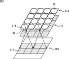
- FIG. 2 is a diagram showing a schematic configuration of the upper substrate 11A and the lower substrate 11B of the solid-state imaging device 1.
- a plurality of pixels 21A are arranged in a two-dimensional array on the upper substrate 11A.
- An on-chip lens 22 is formed in each pixel 21A. Pixel signals obtained by the plurality of pixels 21A arranged on the upper substrate 11A are used as signals for image generation. Therefore, the upper substrate 11A functions as an image sensor.
- a plurality of pixels 21B are also arranged in a two-dimensional array on the lower substrate 11B. Pixel signals obtained by the plurality of pixels 21B arranged on the lower substrate 11B are used as signals for phase difference detection. Therefore, the lower substrate 11B functions as a phase difference detection sensor.
- openings 31 having a size of one pixel that is the same size as the pixel 21A of the upper substrate 11A are formed at predetermined intervals.
- the pixel 21A of the upper substrate 11A includes a pixel that transmits incident light to the lower substrate 11B and a pixel that does not transmit incident light to the lower substrate 11B.
- incident light that has passed through one pixel (hereinafter referred to as a transmissive pixel) of the upper substrate 11A corresponding to the opening 31 of the aperture 12 is 2 ⁇ 2 4 of the lower substrate 11B. It is configured to enter the pixel.
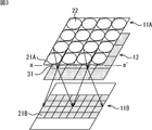
- the incident light that has passed through the transmission pixel of the upper substrate 11A may be received by a plurality of pixels, for example, as shown in FIG. In this way, it can be configured to be incident on 4 ⁇ 4 16 pixels.
- phase difference detection for example, when light that has passed through one transmissive pixel is incident on 2 ⁇ 2 four pixels of the lower substrate 11B, the upper left and lower right pixels of the 2 ⁇ 2 four pixels The focal position can be detected by comparing the signals between the signals and the signals between the upper right and lower left pixels.
- FIGS. 2 and 3 are diagrams for explaining the relationship between the transmissive pixels of the upper substrate 11A and the light-receiving pixels of the lower substrate 11B that receives incident light therefrom.
- the upper substrate 11A and the lower substrate are illustrated in FIG.
- the scale of the pixel size of the substrate 11B is different.
- the focal point of an on-chip lens is ideally the photodiode surface of a silicon layer. Actually, it is located deep in the silicon layer. For this reason, the condensing point for imaging and the condensing point for phase difference detection are different, and there is a problem that it is difficult to achieve optimization of the microlens.
- the focal point of the on-chip lens is set on the surface of the photodiode of the silicon layer, the radius of curvature of the on-chip lens is reduced, and the oblique incidence characteristics are deteriorated. Therefore, as the image height (distance from the optical center) increases, the amount of received light decreases and shading occurs.
- the curvature radius of the on-chip lens is increased by stacking the two substrates 11 and arranging the phase difference detection pixels on the lower substrate 11B. And the occurrence of shading can be suppressed.
- incident light that has passed through one pixel of the upper substrate 11A is received by a plurality of pixels larger than 2 ⁇ 2, so that multi-viewpoint separation can be performed, phase separation pixel separation performance is improved, and phase difference autofocus is achieved. High performance can be achieved.
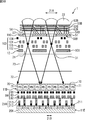
- FIG. 4 is a cross-sectional configuration diagram of the solid-state imaging device 1 taken along the line a-a ′ of FIG.
- the solid-state imaging device 1 is configured by laminating a front side irradiation type upper substrate 11A and a back side irradiation type lower substrate 11B.
- the upper substrate 11A is composed of a silicon layer 51, and light enters from the upper side of the silicon layer 51.
- the green photoelectric conversion film 52G and the red photoelectric conversion film 52R that photoelectrically converts light having a wavelength of R (red) are stacked.
- Transparent electrodes 53B, 53G, and 53R are formed for the respective pixels 21A on the lower surfaces of the blue photoelectric conversion film 52B, the green photoelectric conversion film 52G, and the red photoelectric conversion film 52R.
- the transparent electrodes 53B, 53G, and 53R are connected to the transistor circuits 55B, 55G, and 55R formed in the silicon layer 51 through connection electrodes 54B, 54G, and 54R, respectively.
- the upper surface of the silicon layer 51 is protected by an insulating film 56.
- the transparent electrodes 53B, 53G, and 53R, the connection electrodes 54B, 54G, and 54R, and the transistor circuits 55B, 55G, and 55R are related to B in order to prevent the drawing from being complicated. Only one of each of the transparent electrode 53B, the connection electrode 54B, and the transistor circuit 55B is provided with a reference numeral.
- a transparent electrode to which a predetermined voltage such as a power supply voltage or GND is supplied may be formed on the upper surface of each of the blue photoelectric conversion film 52B, the green photoelectric conversion film 52G, and the red photoelectric conversion film 52R.
- the photoelectric conversion film 52 (52B, 52G, 52R) functions as a photoelectric conversion unit, and the transistor circuit 55 (55B, 55G, 55R) functions as a charge detection unit that detects charges photoelectrically converted by the photoelectric conversion unit.
- the photoelectric conversion film 52 is formed over the entire surface of the light receiving region. However, since the transparent electrode 53 is separately formed for each pixel, R, G, and B pixel signals can be acquired in units of pixels. .
- the photoelectric conversion film 52 can be composed of, for example, an organic photoelectric conversion film.
- an organic photoelectric conversion material containing a coumarin dye, tris-8-hydroxyquinoline Al (Alq3), a melocyanine dye, or the like can be used.
- an organic photoelectric conversion material containing a rhodamine dye, a melocyanine dye, quinacridone, or the like can be used.
- An organic photoelectric conversion material containing a phthalocyanine dye can be used as the red photoelectric conversion film 52R that performs photoelectric conversion with R wavelength light.
- the photoelectric conversion film 52 may be composed of an inorganic photoelectric conversion film.
- the inorganic photoelectric conversion film is formed of, for example, CuInSe2 (CIS-based thin film) that is a semiconductor thin film having a chalcopyrite structure, or Cu (In, Ga) Se2 (CIGS-based thin film) in which Ga is dissolved. Can do.
- a metal film 61 as the aperture 12 is formed below the silicon layer 51, and an opening 31 is formed in the transmissive pixel portion of the metal film 61.
- the metal film 61 is covered with a protective film 62.
- a transparent layer 57 that totally transmits incident light is formed in a region corresponding to the opening 31 of the silicon layer 51.
- the transparent layer 57 can be formed of, for example, SiO2 obtained by oxidizing silicon (Si).
- the photoelectric conversion film 52 as a photoelectric conversion portion is formed on the upper side of the silicon layer 51 and no photodiode is formed on the silicon layer 51, the thickness of the silicon layer 51 is extremely thin. can do. Therefore, the silicon layer 51 can be used as it is because the light can be sufficiently transmitted without forming the transparent layer 57 without changing the silicon layer 51.
- the lower substrate 11B is constituted by a silicon layer 70, and a photodiode (PD) 71 as a photoelectric conversion unit is formed in each silicon pixel 70 by a pn junction.
- PD photodiode
- the focal length of the on-chip lens 22 is such that light incident on the transmissive pixels of the upper substrate 11A is incident on the four-pixel photodiodes 71 of the lower substrate 11B. Accordingly, a protective film 72 and an intermediate layer 73 are formed.
- the protective film 72 can be formed by, for example, a silicon oxide film or a silicon nitride film, and the intermediate layer 73 can be formed by, for example, a glass layer. Further, the intermediate layer 73 may be made of the same material as that of the protective film 72.
- the lower substrate 11B is a back-illuminated type, the lower substrate 11B and the upper substrate 11A are bonded so that the opposite side of the multilayer wiring layer 84 formed on the silicon layer 70 is the upper substrate 11A side. Yes.
- the multilayer wiring layer 84 includes a plurality of transistor circuits 81, one or more wiring layers 82, an interlayer insulating film 83, and the like that constitute a reading circuit that reads out signal charges accumulated in the photodiode 71.
- the upper substrate 11A outputs R, G, and B pixel signals for each pixel 21A, and has a function as a color image sensor. Further, the lower substrate 11B outputs a phase difference signal obtained by receiving light having passed through the upper substrate 11A by a plurality of pixels 21B (multi-viewpoint), and has a function as a phase difference sensor.
- the photoelectric conversion film 52 when used as a photoelectric conversion unit, since color separation and light reception can be performed simultaneously with a thin film, the aperture ratio is high, and the on-chip lens 22 is basically unnecessary. . Therefore, the on-chip lens 22 can be formed to have a long focal length in accordance with the incidence on the plurality of photodiodes 71 on the lower substrate 11B. Therefore, acquisition of the image signal and the phase difference signal can be realized without deteriorating the oblique incidence characteristic.
- the solid-state imaging device 1 it is possible to suppress the deterioration of the oblique incidence characteristics and reduce the occurrence of shading, so that the image quality of the captured image can be improved.
- incident light that has passed through the transmissive pixels on the upper substrate 11A is reduced by increasing the interval (thinning) of the transmissive pixels on the upper substrate 11A or adjusting the thickness of the intermediate layer 73. It is possible to arbitrarily adjust how many pixels of the side substrate 11B are made incident. For example, the resolution in the distance direction (phase difference resolution) is improved by making multiple viewpoints so that light from one transmission pixel is incident on 16 ⁇ 4 ⁇ 4 pixels instead of 4 ⁇ 2 ⁇ 2 pixels. The distance measuring performance can also be improved.
- the upper substrate 11A performs photoelectric conversion by the photoelectric conversion film 52 formed outside the silicon layer 51, it is not necessary to form a photodiode in the silicon layer 51, and only the transistor circuit 55 needs to be formed.
- the thickness of 51 can be made extremely thin. Thereby, the transmittance of light having a wavelength of G (green) or more of the silicon layer 51 can be significantly increased, so that the amount of light incident on the photodiode 71 of the lower substrate 11B can be increased.
- the transparent pixel region of the silicon layer 51 of the upper substrate 11A is the transparent layer 57 that totally transmits light
- the amount of light incident on the photodiode 71 of the lower substrate 11B can be further increased.
- the photoelectric conversion film 52 has a high absorptance and the amount of light incident on the lower substrate 11B of R, G, B light is small, near infrared light other than visible light can be used for phase difference detection. That's fine.
- FIG. 5 is a cross-sectional configuration diagram illustrating a modified example of the solid-state imaging device 1 according to the first embodiment.
- the on-chip lens 22 is not necessary for the photoelectric conversion film 52. Therefore, if the solid-state imaging device 1 has some structure for condensing incident light onto the lower substrate 11B, the on-chip lens 22 above the stacked photoelectric conversion film 52 can be omitted. .
- an in-layer lens 91 is provided below the aperture 12 instead of the on-chip lens 22, and incident light is condensed onto the lower substrate 11 ⁇ / b> B by the in-layer lens 91. You can also.
- the in-layer lens 91 may be disposed not on the lower side of the aperture 12 but on the upper side of the aperture 12, for example, or on any other layer.
- the intralayer lens 91 may be formed only in the transmissive pixel, or may be formed flat in a pixel region where the opening 31 is not formed.
- the position of the aperture 12 is not limited to the lower side of the silicon layer 51 but may be the upper side of the silicon layer 51.
- FIG. 6 is a cross-sectional configuration diagram illustrating the second embodiment of the solid-state imaging device 1 according to the present disclosure.
- the upper substrate 11A may be a back-illuminated type
- the lower substrate 11B may be a front-illuminated type. That is, each of the upper side substrate 11A and the lower side substrate 11B may adopt either a front side irradiation type or a back side irradiation type configuration.
- a configuration example is formed in which both the upper substrate 11A and the lower substrate 11B are stacked as a backside illumination type.
- the upper substrate 11A is changed to the back-illuminated type as compared with the first embodiment shown in FIG.
- the multilayer wiring layer 103 is formed on the side opposite to the light incident side of the upper substrate 11A (below the upper substrate 11A in FIG. 6).
- the multilayer wiring layer 103 includes one or more wiring layers 101 and an interlayer insulating film 102.
- the aperture 12 can be formed by one wiring layer 101 in the multilayer wiring layer 103 as shown in FIG.
- the photoelectric conversion portion is not limited to three layers, and may be a photoelectric conversion film 52 having two layers, one layer, or four layers or more.
- FIG. 7 is a cross-sectional configuration diagram illustrating a third embodiment of the solid-state imaging device 1 according to the present disclosure, and illustrates a configuration example in which the photoelectric conversion unit is a two-layer photoelectric conversion film 52.
- the two-layer photoelectric conversion film 52 is formed on the upper side of the semiconductor substrate 11A on the light incident surface side.
- a green photoelectric conversion film 52G that photoelectrically converts light having a G (green) wavelength is formed over the entire surface.
- the lower photoelectric conversion film 52 of the two layers includes a red photoelectric conversion film 52R that photoelectrically converts light of R (red) wavelength and a blue photoelectric that photoelectrically converts light of B (blue) wavelength. Any one of the conversion films 52B is formed separately for each pixel. Each of the red photoelectric conversion film 52R and the blue photoelectric conversion film 52B is formed in a checkered pattern so that the color (wavelength) of light to be photoelectrically converted is different in, for example, pixels adjacent in the vertical and horizontal directions. .
- the charge photoelectrically converted by the green photoelectric conversion film 52G is taken out by the transistor circuit 55G formed in the silicon layer 51 through the transparent electrode 53G and the connection electrode 54G formed in pixel units.
- the charge photoelectrically converted by the blue photoelectric conversion film 52B is taken out by the transistor circuit 55B formed in the silicon layer 51 through the transparent electrode 53B and the connection electrode 54B formed in pixel units.
- the red photoelectric conversion film 52R is taken out by the transistor circuit 55B formed in the silicon layer 51 through the transparent electrode 53B and the connection electrode 54B formed in pixel units. The same applies to the red photoelectric conversion film 52R.
- the lower photoelectric conversion film 52 of the two layers of the photoelectric conversion film 52 has the B wavelength.
- R wavelength light which is light that has not been absorbed by the upper green photoelectric conversion film 52G and the lower blue photoelectric conversion film 52B, is incident on the lower substrate 11B.
- phase difference detection can be performed based on the amount of received light of R wavelength.
- the pixel 21A (hereinafter referred to as an R non-absorbing pixel) in which light of R wavelength is not absorbed. ) Is arranged every other pixel, and all R non-absorbing pixels can be transmissive pixels.
- a pixel 21A that is a transmission pixel by arranging the opening 31 and a pixel that is shielded by the aperture 12 without the opening 31 being arranged.
- 21A there is 21A.
- the sensitivity characteristic may be different between a transmissive pixel and a non-transparent pixel.
- all R non-absorbing pixels are transmissive pixels in order to prevent the occurrence of a characteristic difference due to the presence or absence of the opening 31.
- all the pixels in which the two-layer photoelectric conversion film 52 is a combination of the green photoelectric conversion film 52G and the blue photoelectric conversion film 52B are transmissive pixels.
- the blue photoelectric conversion films 52B are arranged every other pixel, all the R non-absorbing pixels can be made transmissive pixels.
- the arrangement of the transmissive pixels is limited to the pixel 21A that is a combination of the green photoelectric conversion film 52G and the blue photoelectric conversion film 52B.
- the wavelength of light to be photoelectrically converted is Since all the pixels are common, any pixel may be used as the transmissive pixel, and the arrangement (pitch) of the transmissive pixels in the light receiving region can be arbitrarily set.
- the pixel 21A on which the blue photoelectric conversion film 52B is formed is a transmission pixel.
- the pixel 21A on which the film 52R is formed may be a transmissive pixel. In this case, light having a wavelength of B is incident on the lower substrate 11B, and phase difference detection is performed based on the amount of light received by B.
- the upper photoelectric conversion film 52 is a blue photoelectric conversion film 52B that photoelectrically converts light having the B wavelength, or a red photoelectric conversion film that photoelectrically converts light having the R wavelength. 52R may be used.
- the wavelength of light photoelectrically converted by the lower photoelectric conversion film 52 can also be appropriately changed according to the wavelength of photoelectric conversion by the upper photoelectric conversion film 52. That is, in which layer of the photoelectric conversion film 52, which layer of light with which wavelength is subjected to photoelectric conversion can be determined as appropriate.
- the arrangement of the lower-layer two-color photoelectric conversion films 52 in the checkered pattern in the third embodiment can also be determined as appropriate.
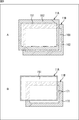
- FIG. 8 shows a circuit arrangement configuration example of each substrate 11 of the upper substrate 11A and the lower substrate 11B.
- the light receiving region 151 of the upper substrate 11A and the light receiving region 161 of the lower substrate 11B have the same size, and the coverage of the phase difference sensor region of the lower substrate 11B with respect to the light receiving region 151 of the upper substrate 11A is 100%.
- a circuit arrangement configuration example is shown.
- the circuit area 152 of the upper substrate 11A and the circuit area 162 of the lower substrate 11B have the same size.
- the light receiving region 151 is about 15.75 mm ⁇ 23.6 mm.
- FIG. 8B shows a circuit arrangement configuration example of each substrate 11 of the upper substrate 11A and the lower substrate 11B when the size of one chip is reduced as much as possible without reducing the light receiving sensitivity of the image sensor.
- Only the light receiving region 151 is formed on the upper substrate 11A.
- a light receiving region 171 as a phase difference sensor region and a circuit region 172 are formed on the lower substrate 11B.
- the circuit region 172 the circuits of the circuit region 152 of the upper substrate 11A and the circuit region 162 of the lower substrate 11B in FIG. Therefore, the size of the circuit region 172 is larger than the size of the circuit region 162 of the lower substrate 11B in FIG.
- the solid-state imaging device 1 can be configured by a stacked structure of three or more substrates 11 in addition to the stacked structure of the two substrates 11 described above.
- FIG. 9 shows a circuit arrangement configuration example of each substrate 11 in the case where the solid-state imaging device 1 is configured by a laminated structure of three substrates 11.
- Only the light receiving region 151 is formed on the upper substrate 11C that is the uppermost layer of the three-layer structure, and the intermediate substrate 11D that is the intermediate layer is the same size as the light receiving region 151 with respect to the light receiving region 151 of the upper substrate 11C.
- a light receiving region 161 having a coverage ratio of the phase difference sensor region of 100% is formed.
- a circuit region 181 is formed in the lower substrate 11E which is the lowest layer of the three-layer structure.
- the chip size is reduced as compared with the solid-state imaging device 1 having the two-layer structure of FIG. can do. Further, the coverage of the phase difference sensor region can be ensured to be larger than that of the solid-state imaging device 1 having the two-layer structure of B in FIG.
- the entire area of the lower substrate 11E which is the lowermost layer, can be used as the circuit area 181, other than the drive circuit that drives each pixel of the light receiving area 151 of the upper substrate 11C and the light receiving area 161 of the intermediate substrate 11E.
- An ADC Analog-Digital Converter
- a logic circuit a memory, and the like can also be arranged in the circuit region 181 of the lower substrate 11E.
- phase difference auto The detection speed of focus can be improved.
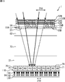
- FIG. 10 is a cross-sectional configuration diagram in the case where the solid-state imaging device 1, which is a fourth embodiment of the solid-state imaging device 1, is configured by a laminated structure of three substrates 11.
- the upper substrate 11C and the intermediate substrate 11D correspond to the upper substrate 11A and the lower substrate 11B of the solid-state imaging device 1 having the three-layer photoelectric conversion film 52 shown in FIG. Both the upper substrate 11C and the intermediate substrate 11D are bonded so as to be a back-illuminated type.
- the multilayer wiring layer 84 of the intermediate substrate 11D and the multilayer wiring layer 214 of the lower substrate 11E are joined by, for example, a Cu—Cu metal bond.
- the multilayer wiring layer 214 is composed of one or more wiring layers 212 and an interlayer insulating film 213.
- a broken line between the wiring layer 82 and the wiring layer 212 represents a bonding surface between the intermediate substrate 11D and the lower substrate 11E.
- a signal processing circuit including a plurality of transistor circuits 211 and the like is formed on the silicon layer 201 of the lower substrate 11E.
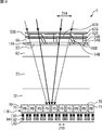
- FIG. 11 shows another cross-sectional configuration diagram in the case where the solid-state imaging device 1 is configured by a laminated structure of three substrates 11.
- the upper substrate 11C and the intermediate substrate 11D correspond to the upper substrate 11A and the lower substrate 11B of the solid-state imaging device 1 having the two-layer photoelectric conversion film 52 shown in FIG. Both the upper substrate 11C and the intermediate substrate 11D are bonded so as to be a back-illuminated type.
- the multilayer wiring layer 84 of the intermediate substrate 11D and the multilayer wiring layer 214 of the lower substrate 11E are joined by, for example, a Cu—Cu metal bond.
- the multilayer wiring layer 214 is composed of one or more wiring layers 212 and an interlayer insulating film 213.
- a broken line between the wiring layer 82 and the wiring layer 212 represents a bonding surface between the intermediate substrate 11D and the lower substrate 11E.
- a signal processing circuit including a plurality of transistor circuits 211 and the like is formed on the silicon layer 201 of the lower substrate 11E.
- the pixel signal obtained from the upper substrate 11A is used as a signal for obtaining a captured image
- the pixel signal obtained from the lower substrate 11B is used as a signal for detecting a phase difference. It was a configuration to use.
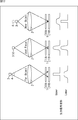
- FIG. 12 is a diagram for explaining the focus control of the contrast method performed by the solid-state imaging device 1.
- Focus control can be performed by comparing the contrast of images obtained on the lower substrate 11B.
- the adjustment direction of the autofocus can be known, so that the autofocus is performed at high speed. be able to.
- the distance to the subject 3 from the difference between the contrast of the image obtained on the upper substrate 11A and the contrast of the image obtained on the lower substrate 11B. It is also possible to combine them.
- FIG. 13 is a cross-sectional configuration diagram illustrating a fifth embodiment of the solid-state imaging device 1 according to the present disclosure, and illustrates a configuration example in the case of performing focus control by a contrast method.
- the configuration according to the fifth embodiment shown in FIG. 13 is compared with the configuration according to the first embodiment shown in FIG. 4, in the fifth embodiment, the on-chip lens 22 and the aperture 12 are compared.
- the difference from the configuration according to the first embodiment is that the (metal film 61) is not formed.
- the on-chip lens 22 is not necessary when the photoelectric conversion part of the upper substrate 11A is constituted by the photoelectric conversion film 52.
- the optical lens 2 (FIG. 1) may be configured such that incident light is imaged on the upper surface of the photodiode 71 of the lower substrate 11B. In this case, the on-chip lens 22 is not necessary.
- the pixel 21A other than the transmissive pixel has to be shielded by the aperture 12.
- the aperture 12 is also unnecessary.
- the solid-state imaging device 1 allows the contrast between the pixel signal obtained by the photoelectric conversion film 52 of the upper substrate 11A and the pixel signal obtained by the photodiode 71 of the lower substrate 11B. Focus control can be performed by comparing the differences.
- the light incident on the photodiode 71 of the lower substrate 11B is not near visible light. Infrared light.
- focus control can be performed by comparison with a pixel signal obtained by the photoelectric conversion film 52 of the upper substrate 11A that photoelectrically converts light having the same color as the light that can be received by the lower substrate 11B.
- focus control is performed by comparing the contrast difference between the pixel signal obtained by the red photoelectric conversion film 52R of the upper substrate 11A and the pixel signal obtained by the photodiode 71 of the lower substrate 11B. be able to.
- a laminated structure of three substrates 11 can be used.
- the solid-state imaging device 1 described above can be applied to various electronic devices such as an imaging device such as a digital still camera or a digital video camera, a mobile phone having an imaging function, or an audio player having an imaging function. .
- FIG. 15 is a block diagram illustrating a configuration example of an imaging apparatus as an electronic apparatus according to the present disclosure.
- An imaging apparatus 301 shown in FIG. 15 includes an optical system 302, a shutter device 303, a solid-state imaging device 304, a control circuit 305, a signal processing circuit 306, a monitor 307, and a memory 308, and displays still images and moving images. Imaging is possible.
- the optical system 302 includes one or a plurality of lenses, guides light (incident light) from the subject to the solid-state image sensor 304, and forms an image on the light-receiving surface of the solid-state image sensor 304.
- the shutter device 303 is disposed between the optical system 302 and the solid-state imaging device 304, and controls the light irradiation period and the light-shielding period to the solid-state imaging device 304 according to the control of the control circuit 305.
- the solid-state image sensor 304 is configured by the solid-state image sensor 1 described above.
- the solid-state imaging device 304 accumulates signal charges for a certain period in accordance with light imaged on the light receiving surface via the optical system 302 and the shutter device 303.
- the signal charge accumulated in the solid-state image sensor 304 is transferred according to a drive signal (timing signal) supplied from the control circuit 305.
- the solid-state imaging device 304 may be configured as a single chip by itself or may be configured as a part of a camera module packaged together with the optical system 302 or the signal processing circuit 306.
- the control circuit 305 outputs a drive signal for controlling the transfer operation of the solid-state image sensor 304 and the shutter operation of the shutter device 303 to drive the solid-state image sensor 304 and the shutter device 303.
- the signal processing circuit 306 performs various kinds of signal processing on the pixel signal output from the solid-state imaging device 304.
- An image (image data) obtained by the signal processing by the signal processing circuit 306 is supplied to the monitor 307 and displayed, or supplied to the memory 308 and stored (recorded).
- the solid-state imaging device 1 By using the solid-state imaging device 1 according to each of the above-described embodiments as the solid-state imaging device 304, it is possible to suppress the occurrence of shading and realize high-speed and high-precision autofocus. Therefore, the image quality of captured images can be improved also in the imaging device 301 such as a video camera, a digital still camera, and a camera module for mobile devices such as a mobile phone.
- the imaging device 301 such as a video camera, a digital still camera, and a camera module for mobile devices such as a mobile phone.
- the substrate 11 may adopt either an impurity region configuration in which electrons are signal charges or an impurity region configuration in which holes are signal charges. Further, in each of the above-described embodiments, the transistor circuits 55 and 81 as the charge detection unit are formed on the substrate 11 (silicon substrate). However, the transistor circuits 55 and 81 may be organic transistors.
- this indication can also take the following structures.
- Two or more photoelectric conversion layers including a photoelectric conversion part and a charge detection part are laminated, Including a state in which light incident on one pixel of the first photoelectric conversion layer on the side close to the optical lens is received by the photoelectric conversion units of the plurality of pixels on the second photoelectric conversion layer on the side far from the optical lens.
- Solid-state imaging device configured as follows. (2) The solid-state imaging device according to (1), wherein the photoelectric conversion unit of the first photoelectric conversion layer includes a photoelectric conversion film. (3) The said photoelectric conversion film is an organic photoelectric conversion film. The solid-state image sensor as described in said (1) or (2).
- the solid-state imaging device according to (1) or (2), wherein the photoelectric conversion film is an inorganic photoelectric conversion film.
- the photoelectric conversion unit of the first photoelectric conversion layer includes a three-layer photoelectric conversion film.
- the three-layer photoelectric conversion film photoelectrically converts a first photoelectric conversion film that photoelectrically converts light having a blue wavelength, a second photoelectric conversion film that photoelectrically converts light having a green wavelength, and light having a red wavelength.
- the solid-state imaging device which is a third photoelectric conversion film.
- the solid-state imaging device according to any one of (1) to (5), wherein the photoelectric conversion unit of the first photoelectric conversion layer includes a two-layer photoelectric conversion film.
- the first layer of the two-layer photoelectric conversion film is a photoelectric conversion film that photoelectrically converts light of any one color of red, green, and blue
- the second layer of the two-layer photoelectric conversion film is a photoelectric conversion film that photoelectrically converts the remaining two colors of red, green, and blue.
- the solid-state imaging device according to (8).
- the first layer of the first photoelectric conversion film photoelectrically converts green light
- the second layer of the second photoelectric conversion film photoelectrically converts red and blue light.
- the solid-state imaging device according to (9).
- (11) The solid-state imaging device according to any one of (1) to (10), wherein the charge detection unit includes a transistor circuit formed in a silicon layer.
- (12) The solid-state imaging device according to any one of (1) to (11), wherein the photoelectric conversion unit of the second photoelectric conversion layer includes a photodiode.
- (13) The solid-state imaging device according to any one of (1) to (12), wherein a pixel signal obtained by a plurality of pixels of the second photoelectric conversion layer is a signal for detecting a phase difference.
- the pixel signal obtained from the first photoelectric conversion layer and the pixel signal obtained from the second photoelectric conversion layer are compared to perform focus control.
- (1) to (12) The solid-state imaging device according to any one of the above.
- the pixel of the first photoelectric conversion layer includes a pixel that transmits the light to the second photoelectric conversion layer and a pixel that does not transmit the light to the second photoelectric conversion layer.
- the semiconductor substrate on which the charge detection unit of the first photoelectric conversion layer is formed is a surface irradiation type.
- the solid-state imaging device according to any one of (1) to (16), wherein the semiconductor substrate on which the charge detection unit of the first photoelectric conversion layer is formed is a backside illumination type. (19) In addition to the two semiconductor substrates on which the first photoelectric conversion layer and the second photoelectric conversion layer are formed, a semiconductor substrate on which a signal processing circuit is formed is laminated. (1) to (18) ). (20) Two or more photoelectric conversion layers including a photoelectric conversion part and a charge detection part are laminated, Including a state in which light incident on one pixel of the first photoelectric conversion layer on the side close to the optical lens is received by the photoelectric conversion units of the plurality of pixels on the second photoelectric conversion layer on the side far from the optical lens.
- An electronic device comprising a solid-state imaging device configured as described above.
- 1 solid-state imaging device 2 optical lens, 11A, 11B semiconductor substrate, 12 aperture, 11D, 11E semiconductor substrate, 21A, 21B pixel, 22 on-chip lens, 31 aperture, 51 silicon layer, 52 photoelectric conversion film, 53 transparent electrode , 54 connection electrodes, 55 transistor circuit, 70 silicon layer, 71 photodiode, 201 silicon layer, 211 transistor circuit, 301 imaging device, 304 solid-state imaging device
Landscapes
- Physics & Mathematics (AREA)
- Engineering & Computer Science (AREA)
- General Physics & Mathematics (AREA)
- Optics & Photonics (AREA)
- Multimedia (AREA)
- Signal Processing (AREA)
- Computer Vision & Pattern Recognition (AREA)
- Solid State Image Pick-Up Elements (AREA)
- Transforming Light Signals Into Electric Signals (AREA)
- Focusing (AREA)
- Automatic Focus Adjustment (AREA)
- Color Television Image Signal Generators (AREA)
Abstract
Description
1.第1の実施の形態(上側基板が表面照射型の構成例)
2.第2の実施の形態(上側基板が裏面照射型の構成例)
3.第3の実施の形態(光電変換膜が2層の場合の構成例)
4.第4の実施の形態(3枚の基板の積層構造で構成される構成例)
5.第5の実施の形態(コントラストAFを採用した構成例)
6.電子機器への適用例
<撮像機構の構成>
図1は、本開示に係る固体撮像素子を含む撮像機構を示す図である。
図5は、第1の実施の形態に係る固体撮像素子1の変形例を示す断面構成図である。
図6は、本開示に係る固体撮像素子1の第2の実施の形態を示す断面構成図である。
図4に示した第1の実施の形態の断面構成では、R、G、Bそれぞれについて1層ずつ光電変換膜52が設けられ、光電変換部が、3層の光電変換膜52を積層した構成とされていた。
図8は、上側基板11Aと下側基板11Bの各基板11の回路配置構成例を示している。
また、固体撮像素子1は、上述した2枚の基板11による積層構造の他、3枚以上の基板11による積層構造で構成することもできる。
<3層構造の構成例1>
図10は、固体撮像素子1の第4の実施の形態である、固体撮像素子1が3枚の基板11の積層構造で構成される場合の断面構成図を示している。
図11は、固体撮像素子1が3枚の基板11の積層構造で構成される場合のその他の断面構成図を示している。
上述した第1乃至第3の実施の形態は、上側基板11Aで得られる画素信号については撮像画像を求める信号として利用し、下側基板11Bで得られる画素信号については位相差検出を行う信号として利用する構成であった。
図12は、固体撮像素子1が行うコントラスト法のフォーカス制御を説明する図である。
上述した固体撮像素子1は、例えば、デジタルスチルカメラやデジタルビデオカメラなどの撮像装置、撮像機能を備えた携帯電話機、または、撮像機能を備えたオーディオプレーヤといった各種の電子機器に適用することができる。
(1)
光電変換部と電荷検出部を含む光電変換層が2層以上積層されており、
光学レンズに近い側の第1の光電変換層の1画素に入射された光が、前記光学レンズから遠い側の第2の光電変換層の複数画素の前記光電変換部で受光される状態を含むように構成されている
固体撮像素子。
(2)
前記第1の光電変換層の前記光電変換部は、光電変換膜で構成されている
前記(1)に記載の固体撮像素子。
(3)
前記光電変換膜は、有機光電変換膜である
前記(1)または(2)に記載の固体撮像素子。
(4)
前記光電変換膜は、無機光電変換膜である
前記(1)または(2)に記載の固体撮像素子。
(5)
前記第1の光電変換層の前記光電変換部は、2層以上の光電変換膜で構成されている
前記(1)乃至(4)のいずれかに記載の固体撮像素子。
(6)
前記第1の光電変換層の前記光電変換部は、3層の光電変換膜で構成されている
前記(1)乃至(5)のいずれかに記載の固体撮像素子。
(7)
前記3層の光電変換膜は、青色の波長の光を光電変換する第1光電変換膜と、緑色の波長の光を光電変換する第2光電変換膜と、赤色の波長の光を光電変換する第3光電変換膜である
前記(6)に記載の固体撮像素子。
(8)
前記第1の光電変換層の前記光電変換部は、2層の光電変換膜で構成されている
前記(1)乃至(5)のいずれかに記載の固体撮像素子。
(9)
前記2層の光電変換膜の第1層は、赤色、緑色、及び青色のいずれか1色の光を光電変換する光電変換膜であり、
前記2層の光電変換膜の第2層は、前記赤色、緑色、及び青色の残りの2色の光を光電変換する光電変換膜である
前記(8)に記載の固体撮像素子。
(10)
前記第1光電変換膜の第1層は、緑色の光を光電変換し、
前記第2光電変換膜の第2層は、赤色と青色の光を光電変換する
前記(9)に記載の固体撮像素子。
(11)
前記電荷検出部は、シリコン層に形成されたトランジスタ回路で構成される
前記(1)乃至(10)のいずれかに記載の固体撮像素子。
(12)
前記第2の光電変換層の前記光電変換部は、フォトダイオードで構成される
前記(1)乃至(11)のいずれかに記載の固体撮像素子。
(13)
前記第2の光電変換層の複数画素で得られる画素信号は、位相差検出用の信号である
前記(1)乃至(12)のいずれかに記載の固体撮像素子。
(14)
前記第1の光電変換層で得られる画素信号と、前記第2の光電変換層で得られる画素信号とを比較して、フォーカス制御を行うように構成されている
前記(1)乃至(12)のいずれかに記載の固体撮像素子。
(15)
前記第1の光電変換層の画素は、前記光を前記第2の光電変換層へ透過させる画素と、前記第2の光電変換層へ透過させない画素を含む
前記(1)乃至(14)のいずれかに記載の固体撮像素子。
(16)
前記第1の光電変換層と前記第2の光電変換層は、2枚の半導体基板を用いて形成される
前記(1)乃至(15)のいずれかに記載の固体撮像素子。
(17)
前記第1の光電変換層の前記電荷検出部が形成された前記半導体基板は、表面照射型である
前記(1)乃至(16)のいずれかに記載の固体撮像素子。
(18)
前記第1の光電変換層の前記電荷検出部が形成された前記半導体基板は、裏面照射型である
前記(1)乃至(16)のいずれかに記載の固体撮像素子。
(19)
前記第1の光電変換層と前記第2の光電変換層が形成された前記2枚の半導体基板に加えて、信号処理回路が形成された半導体基板が積層されている
前記(1)乃至(18)のいずれかに記載の固体撮像素子。
(20)
光電変換部と電荷検出部を含む光電変換層が2層以上積層されており、
光学レンズに近い側の第1の光電変換層の1画素に入射された光が、前記光学レンズから遠い側の第2の光電変換層の複数画素の前記光電変換部で受光される状態を含むように構成されている固体撮像素子
を備える電子機器。
Claims (20)
- 光電変換部と電荷検出部を含む光電変換層が2層以上積層されており、
光学レンズに近い側の第1の光電変換層の1画素に入射された光が、前記光学レンズから遠い側の第2の光電変換層の複数画素の前記光電変換部で受光される状態を含むように構成されている
固体撮像素子。 - 前記第1の光電変換層の前記光電変換部は、光電変換膜で構成されている
請求項1に記載の固体撮像素子。 - 前記光電変換膜は、有機光電変換膜である
請求項2に記載の固体撮像素子。 - 前記光電変換膜は、無機光電変換膜である
請求項2に記載の固体撮像素子。 - 前記第1の光電変換層の前記光電変換部は、2層以上の光電変換膜で構成されている
請求項1に記載の固体撮像素子。 - 前記第1の光電変換層の前記光電変換部は、3層の光電変換膜で構成されている
請求項5に記載の固体撮像素子。 - 前記3層の光電変換膜は、青色の波長の光を光電変換する第1光電変換膜と、緑色の波長の光を光電変換する第2光電変換膜と、赤色の波長の光を光電変換する第3光電変換膜である
請求項6に記載の固体撮像素子。 - 前記第1の光電変換層の前記光電変換部は、2層の光電変換膜で構成されている
請求項5に記載の固体撮像素子。 - 前記2層の光電変換膜の第1層は、赤色、緑色、及び青色のいずれか1色の光を光電変換する光電変換膜であり、
前記2層の光電変換膜の第2層は、前記赤色、緑色、及び青色の残りの2色の光を光電変換する光電変換膜である
請求項8に記載の固体撮像素子。 - 前記第1光電変換膜の第1層は、緑色の光を光電変換し、
前記第2光電変換膜の第2層は、赤色と青色の光を光電変換する
請求項9に記載の固体撮像素子。 - 前記電荷検出部は、シリコン層に形成されたトランジスタ回路で構成される
請求項1に記載の固体撮像素子。 - 前記第2の光電変換層の前記光電変換部は、フォトダイオードで構成される
請求項1に記載の固体撮像素子。 - 前記第2の光電変換層の複数画素で得られる画素信号は、位相差検出用の信号である
請求項1に記載の固体撮像素子。 - 前記第1の光電変換層で得られる画素信号と、前記第2の光電変換層で得られる画素信号とを比較して、フォーカス制御を行うように構成されている
請求項1に記載の固体撮像素子。 - 前記第1の光電変換層の画素は、前記光を前記第2の光電変換層へ透過させる画素と、前記第2の光電変換層へ透過させない画素を含む
請求項1に記載の固体撮像素子。 - 前記第1の光電変換層と前記第2の光電変換層は、2枚の半導体基板を用いて形成される
請求項1に記載の固体撮像素子。 - 前記第1の光電変換層の前記電荷検出部が形成された前記半導体基板は、表面照射型である
請求項16に記載の固体撮像素子。 - 前記第1の光電変換層の前記電荷検出部が形成された前記半導体基板は、裏面照射型である
請求項16に記載の固体撮像素子。 - 前記第1の光電変換層と前記第2の光電変換層が形成された前記2枚の半導体基板に加えて、信号処理回路が形成された半導体基板が積層されている
請求項16に記載の固体撮像素子。 - 光電変換部と電荷検出部を含む光電変換層が2層以上積層されており、
光学レンズに近い側の第1の光電変換層の1画素に入射された光が、前記光学レンズから遠い側の第2の光電変換層の複数画素の前記光電変換部で受光される状態を含むように構成されている固体撮像素子
を備える電子機器。
Priority Applications (6)
| Application Number | Priority Date | Filing Date | Title |
|---|---|---|---|
| US15/325,768 US10554874B2 (en) | 2014-07-22 | 2015-07-10 | Solid-state imaging device and electronic equipment |
| JP2016535872A JP6527868B2 (ja) | 2014-07-22 | 2015-07-10 | 固体撮像素子および電子機器 |
| CN201580037425.2A CN106537594B (zh) | 2014-07-22 | 2015-07-10 | 固体摄像器件和电子设备 |
| US16/732,003 US11728357B2 (en) | 2014-07-22 | 2019-12-31 | Solid-state imaging device and electronic equipment |
| US18/447,882 US12317617B2 (en) | 2014-07-22 | 2023-08-10 | Solid-state imaging device and electronic equipment |
| US19/197,365 US20250267965A1 (en) | 2014-07-22 | 2025-05-02 | Solid-state imaging device and electronic equipment |
Applications Claiming Priority (2)
| Application Number | Priority Date | Filing Date | Title |
|---|---|---|---|
| JP2014-148837 | 2014-07-22 | ||
| JP2014148837 | 2014-07-22 |
Related Child Applications (2)
| Application Number | Title | Priority Date | Filing Date |
|---|---|---|---|
| US15/325,768 A-371-Of-International US10554874B2 (en) | 2014-07-22 | 2015-07-10 | Solid-state imaging device and electronic equipment |
| US16/732,003 Continuation US11728357B2 (en) | 2014-07-22 | 2019-12-31 | Solid-state imaging device and electronic equipment |
Publications (1)
| Publication Number | Publication Date |
|---|---|
| WO2016013410A1 true WO2016013410A1 (ja) | 2016-01-28 |
Family
ID=55162939
Family Applications (1)
| Application Number | Title | Priority Date | Filing Date |
|---|---|---|---|
| PCT/JP2015/069827 Ceased WO2016013410A1 (ja) | 2014-07-22 | 2015-07-10 | 固体撮像素子および電子機器 |
Country Status (4)
| Country | Link |
|---|---|
| US (4) | US10554874B2 (ja) |
| JP (2) | JP6527868B2 (ja) |
| CN (1) | CN106537594B (ja) |
| WO (1) | WO2016013410A1 (ja) |
Cited By (4)
| Publication number | Priority date | Publication date | Assignee | Title |
|---|---|---|---|---|
| JP2018056703A (ja) * | 2016-09-27 | 2018-04-05 | キヤノン株式会社 | 撮像素子および撮像装置 |
| JP2019075554A (ja) * | 2017-10-16 | 2019-05-16 | パナソニックIpマネジメント株式会社 | 撮像装置 |
| US20210223512A1 (en) * | 2018-06-08 | 2021-07-22 | Sony Semiconductor Solutions Corporation | Imaging device |
| KR20230093051A (ko) * | 2020-11-30 | 2023-06-26 | 니폰 덴신 덴와 가부시끼가이샤 | 광학 소자, 촬상 소자 및 촬상장치 |
Families Citing this family (4)
| Publication number | Priority date | Publication date | Assignee | Title |
|---|---|---|---|---|
| US10554874B2 (en) | 2014-07-22 | 2020-02-04 | Sony Semiconductor Solutions Corporation | Solid-state imaging device and electronic equipment |
| CN107302665B (zh) * | 2017-08-18 | 2020-07-24 | 联想(北京)有限公司 | 一种摄像装置、光圈调节方法和电子设备 |
| CN107846537B (zh) * | 2017-11-08 | 2019-11-26 | 维沃移动通信有限公司 | 一种摄像头组件、图像获取方法及移动终端 |
| CN110677606B (zh) * | 2019-09-16 | 2022-06-10 | Oppo广东移动通信有限公司 | 一种像素结构、cis和终端 |
Citations (15)
| Publication number | Priority date | Publication date | Assignee | Title |
|---|---|---|---|---|
| JPS5737336A (en) * | 1980-08-19 | 1982-03-01 | Asahi Optical Co Ltd | Automatic focus detector for camera |
| JP2010239337A (ja) * | 2009-03-31 | 2010-10-21 | Sony Corp | 固体撮像装置、固体撮像装置の信号処理方法および撮像装置 |
| JP2011253861A (ja) * | 2010-05-31 | 2011-12-15 | Fujifilm Corp | 光電変換素子、撮像素子及び光電変換素子の駆動方法 |
| WO2012042963A1 (ja) * | 2010-09-29 | 2012-04-05 | 富士フイルム株式会社 | 固体撮像素子及び撮像装置 |
| JP2013070030A (ja) * | 2011-09-06 | 2013-04-18 | Sony Corp | 撮像素子、電子機器、並びに、情報処理装置 |
| JP2013145292A (ja) * | 2012-01-13 | 2013-07-25 | Nikon Corp | 固体撮像装置および電子カメラ |
| US20130234029A1 (en) * | 2012-03-06 | 2013-09-12 | Omnivision Technologies, Inc. | Image sensor for two-dimensional and three-dimensional image capture |
| JP2013187475A (ja) * | 2012-03-09 | 2013-09-19 | Olympus Corp | 固体撮像装置およびカメラシステム |
| JP2013205516A (ja) * | 2012-03-27 | 2013-10-07 | Nippon Hoso Kyokai <Nhk> | 多重フォーカスカメラ |
| KR101334219B1 (ko) * | 2013-08-22 | 2013-11-29 | (주)실리콘화일 | 3차원 적층구조의 이미지센서 |
| JP2013247548A (ja) * | 2012-05-28 | 2013-12-09 | Olympus Corp | 固体撮像素子および固体撮像装置 |
| JP2014011417A (ja) * | 2012-07-03 | 2014-01-20 | Sony Corp | 固体撮像装置および電子機器 |
| JP2014130890A (ja) * | 2012-12-28 | 2014-07-10 | Canon Inc | 光電変換装置 |
| JP2014232761A (ja) * | 2013-05-28 | 2014-12-11 | キヤノン株式会社 | 固体撮像装置 |
| JP2015128131A (ja) * | 2013-11-27 | 2015-07-09 | ソニー株式会社 | 固体撮像素子および電子機器 |
Family Cites Families (20)
| Publication number | Priority date | Publication date | Assignee | Title |
|---|---|---|---|---|
| DE3131053C2 (de) * | 1980-08-07 | 1983-12-29 | Asahi Kogaku Kogyo K.K., Tokyo | Automatische Fokussierungsermittlungseinrichtung für eine Kamera |
| JP2005252411A (ja) * | 2004-03-01 | 2005-09-15 | Sharp Corp | 固体撮像装置および電子情報機器 |
| JP2005268479A (ja) * | 2004-03-18 | 2005-09-29 | Fuji Film Microdevices Co Ltd | 光電変換膜積層型固体撮像装置 |
| JP5244287B2 (ja) * | 2004-03-19 | 2013-07-24 | 富士フイルム株式会社 | 撮像素子、及び撮像素子に電場を印加する方法 |
| JP4681853B2 (ja) * | 2004-11-11 | 2011-05-11 | 富士フイルム株式会社 | 積層型固体撮像装置 |
| JP4500706B2 (ja) * | 2005-02-23 | 2010-07-14 | 富士フイルム株式会社 | 光電変換膜積層型固体撮像素子 |
| US7812299B2 (en) * | 2005-07-22 | 2010-10-12 | Nikon Corporation | Image sensor having two-dimensionally arrayed pixels, focus detecting device using the sensor, and imaging system including the sensor |
| JP5087304B2 (ja) * | 2007-03-30 | 2012-12-05 | 富士フイルム株式会社 | 固体撮像素子の製造方法 |
| JP5171178B2 (ja) * | 2007-09-13 | 2013-03-27 | 富士フイルム株式会社 | イメージセンサ及びその製造方法 |
| WO2009104417A1 (ja) * | 2008-02-22 | 2009-08-27 | パナソニック株式会社 | 撮像装置 |
| JP5353200B2 (ja) * | 2008-11-20 | 2013-11-27 | ソニー株式会社 | 固体撮像装置および撮像装置 |
| US8593563B2 (en) * | 2009-02-23 | 2013-11-26 | Panasonic Corporation | Imaging device and imaging apparatus including the same |
| KR20110008762A (ko) * | 2009-07-21 | 2011-01-27 | 삼성전자주식회사 | 씨모스 이미지 센서의 단위 화소 및 이를 포함하는 씨모스 이미지 센서 |
| JP5537905B2 (ja) * | 2009-11-10 | 2014-07-02 | 富士フイルム株式会社 | 撮像素子及び撮像装置 |
| JP5199302B2 (ja) * | 2010-03-26 | 2013-05-15 | パナソニック株式会社 | 撮像装置 |
| JP5696513B2 (ja) * | 2011-02-08 | 2015-04-08 | ソニー株式会社 | 固体撮像装置とその製造方法、及び電子機器 |
| US9294691B2 (en) * | 2011-09-06 | 2016-03-22 | Sony Corporation | Imaging device, imaging apparatus, manufacturing apparatus and manufacturing method |
| JP2015170620A (ja) * | 2014-03-04 | 2015-09-28 | 株式会社東芝 | 固体撮像装置 |
| US10554874B2 (en) | 2014-07-22 | 2020-02-04 | Sony Semiconductor Solutions Corporation | Solid-state imaging device and electronic equipment |
| JP6536126B2 (ja) * | 2015-03-31 | 2019-07-03 | 株式会社ニコン | 撮像素子および撮像装置 |
-
2015
- 2015-07-10 US US15/325,768 patent/US10554874B2/en active Active
- 2015-07-10 WO PCT/JP2015/069827 patent/WO2016013410A1/ja not_active Ceased
- 2015-07-10 CN CN201580037425.2A patent/CN106537594B/zh active Active
- 2015-07-10 JP JP2016535872A patent/JP6527868B2/ja active Active
-
2019
- 2019-05-13 JP JP2019090724A patent/JP6724212B2/ja not_active Expired - Fee Related
- 2019-12-31 US US16/732,003 patent/US11728357B2/en active Active
-
2023
- 2023-08-10 US US18/447,882 patent/US12317617B2/en active Active
-
2025
- 2025-05-02 US US19/197,365 patent/US20250267965A1/en active Pending
Patent Citations (15)
| Publication number | Priority date | Publication date | Assignee | Title |
|---|---|---|---|---|
| JPS5737336A (en) * | 1980-08-19 | 1982-03-01 | Asahi Optical Co Ltd | Automatic focus detector for camera |
| JP2010239337A (ja) * | 2009-03-31 | 2010-10-21 | Sony Corp | 固体撮像装置、固体撮像装置の信号処理方法および撮像装置 |
| JP2011253861A (ja) * | 2010-05-31 | 2011-12-15 | Fujifilm Corp | 光電変換素子、撮像素子及び光電変換素子の駆動方法 |
| WO2012042963A1 (ja) * | 2010-09-29 | 2012-04-05 | 富士フイルム株式会社 | 固体撮像素子及び撮像装置 |
| JP2013070030A (ja) * | 2011-09-06 | 2013-04-18 | Sony Corp | 撮像素子、電子機器、並びに、情報処理装置 |
| JP2013145292A (ja) * | 2012-01-13 | 2013-07-25 | Nikon Corp | 固体撮像装置および電子カメラ |
| US20130234029A1 (en) * | 2012-03-06 | 2013-09-12 | Omnivision Technologies, Inc. | Image sensor for two-dimensional and three-dimensional image capture |
| JP2013187475A (ja) * | 2012-03-09 | 2013-09-19 | Olympus Corp | 固体撮像装置およびカメラシステム |
| JP2013205516A (ja) * | 2012-03-27 | 2013-10-07 | Nippon Hoso Kyokai <Nhk> | 多重フォーカスカメラ |
| JP2013247548A (ja) * | 2012-05-28 | 2013-12-09 | Olympus Corp | 固体撮像素子および固体撮像装置 |
| JP2014011417A (ja) * | 2012-07-03 | 2014-01-20 | Sony Corp | 固体撮像装置および電子機器 |
| JP2014130890A (ja) * | 2012-12-28 | 2014-07-10 | Canon Inc | 光電変換装置 |
| JP2014232761A (ja) * | 2013-05-28 | 2014-12-11 | キヤノン株式会社 | 固体撮像装置 |
| KR101334219B1 (ko) * | 2013-08-22 | 2013-11-29 | (주)실리콘화일 | 3차원 적층구조의 이미지센서 |
| JP2015128131A (ja) * | 2013-11-27 | 2015-07-09 | ソニー株式会社 | 固体撮像素子および電子機器 |
Cited By (10)
| Publication number | Priority date | Publication date | Assignee | Title |
|---|---|---|---|---|
| JP2018056703A (ja) * | 2016-09-27 | 2018-04-05 | キヤノン株式会社 | 撮像素子および撮像装置 |
| US11356595B2 (en) | 2016-09-27 | 2022-06-07 | Canon Kabushiki Kaisha | Image sensor and imaging apparatus for outputting image data by discriminating whether to add a result of AF calculation to a captured image data |
| JP2019075554A (ja) * | 2017-10-16 | 2019-05-16 | パナソニックIpマネジメント株式会社 | 撮像装置 |
| US11594562B2 (en) | 2017-10-16 | 2023-02-28 | Panasonic Intellectual Property Management Co., Ltd. | Imaging device |
| JP7474943B2 (ja) | 2017-10-16 | 2024-04-26 | パナソニックIpマネジメント株式会社 | 撮像装置 |
| US12057460B2 (en) | 2017-10-16 | 2024-08-06 | Panasonic Intellectual Property Management Co., Ltd. | Imaging device |
| US20210223512A1 (en) * | 2018-06-08 | 2021-07-22 | Sony Semiconductor Solutions Corporation | Imaging device |
| US12306382B2 (en) * | 2018-06-08 | 2025-05-20 | Sony Semiconductor Solutions Corporation | Imaging device |
| KR20230093051A (ko) * | 2020-11-30 | 2023-06-26 | 니폰 덴신 덴와 가부시끼가이샤 | 광학 소자, 촬상 소자 및 촬상장치 |
| KR102801193B1 (ko) | 2020-11-30 | 2025-04-29 | 니폰 덴신 덴와 가부시끼가이샤 | 광학 소자, 촬상 소자 및 촬상장치 |
Also Published As
| Publication number | Publication date |
|---|---|
| US10554874B2 (en) | 2020-02-04 |
| CN106537594A (zh) | 2017-03-22 |
| US11728357B2 (en) | 2023-08-15 |
| US12317617B2 (en) | 2025-05-27 |
| JPWO2016013410A1 (ja) | 2017-06-08 |
| JP6527868B2 (ja) | 2019-06-05 |
| JP2019169962A (ja) | 2019-10-03 |
| US20170171458A1 (en) | 2017-06-15 |
| CN106537594B (zh) | 2020-02-18 |
| JP6724212B2 (ja) | 2020-07-15 |
| US20250267965A1 (en) | 2025-08-21 |
| US20200162661A1 (en) | 2020-05-21 |
| US20240030244A1 (en) | 2024-01-25 |
Similar Documents
| Publication | Publication Date | Title |
|---|---|---|
| JP6724212B2 (ja) | 固体撮像素子および電子機器 | |
| JP6987950B2 (ja) | 固体撮像素子およびその製造方法、並びに電子機器 | |
| US9686462B2 (en) | Solid-state imaging device and electronic apparatus | |
| US9786714B2 (en) | Solid-state imaging element, method for manufacturing solid-state imaging element, and electronic device | |
| WO2016002574A1 (ja) | 固体撮像素子および電子機器 | |
| JP2012018951A (ja) | 固体撮像素子及びその製造方法、並びに固体撮像装置及び撮像装置 | |
| JP2008227250A (ja) | 複合型固体撮像素子 | |
| JP2014232761A (ja) | 固体撮像装置 | |
| JP5504382B2 (ja) | 固体撮像素子及び撮像装置 | |
| JP5331119B2 (ja) | 固体撮像素子および撮像装置 | |
| JP6633850B2 (ja) | 積層型固体撮像素子 | |
| WO2020070887A1 (ja) | 固体撮像装置 | |
| JP2010040997A (ja) | 固体撮像素子 |
Legal Events
| Date | Code | Title | Description |
|---|---|---|---|
| 121 | Ep: the epo has been informed by wipo that ep was designated in this application |
Ref document number: 15825050 Country of ref document: EP Kind code of ref document: A1 |
|
| ENP | Entry into the national phase |
Ref document number: 2016535872 Country of ref document: JP Kind code of ref document: A |
|
| WWE | Wipo information: entry into national phase |
Ref document number: 15325768 Country of ref document: US |
|
| NENP | Non-entry into the national phase |
Ref country code: DE |
|
| 122 | Ep: pct application non-entry in european phase |
Ref document number: 15825050 Country of ref document: EP Kind code of ref document: A1 |