WO2015198523A1 - 磁性薄膜および磁性薄膜を含む応用デバイス - Google Patents
磁性薄膜および磁性薄膜を含む応用デバイス Download PDFInfo
- Publication number
- WO2015198523A1 WO2015198523A1 PCT/JP2015/002519 JP2015002519W WO2015198523A1 WO 2015198523 A1 WO2015198523 A1 WO 2015198523A1 JP 2015002519 W JP2015002519 W JP 2015002519W WO 2015198523 A1 WO2015198523 A1 WO 2015198523A1
- Authority
- WO
- WIPO (PCT)
- Prior art keywords
- magnetic
- layer
- thin film
- magnetic recording
- magnetic thin
- Prior art date
Links
- 230000005291 magnetic effect Effects 0.000 title claims abstract description 267
- 239000010409 thin film Substances 0.000 title claims abstract description 55
- 239000000956 alloy Substances 0.000 claims abstract description 43
- 229910045601 alloy Inorganic materials 0.000 claims abstract description 42
- 229910052742 iron Inorganic materials 0.000 claims abstract description 6
- 229910052759 nickel Inorganic materials 0.000 claims abstract description 6
- 229910052737 gold Inorganic materials 0.000 claims abstract description 5
- 229910052741 iridium Inorganic materials 0.000 claims abstract description 5
- 229910052763 palladium Inorganic materials 0.000 claims abstract description 5
- 229910052697 platinum Inorganic materials 0.000 claims abstract description 5
- 239000013078 crystal Substances 0.000 claims description 35
- 239000000758 substrate Substances 0.000 claims description 34
- 239000000463 material Substances 0.000 claims description 28
- 230000004888 barrier function Effects 0.000 claims description 13
- 229910052796 boron Inorganic materials 0.000 claims description 5
- 150000004767 nitrides Chemical class 0.000 claims description 5
- OKTJSMMVPCPJKN-UHFFFAOYSA-N Carbon Chemical compound [C] OKTJSMMVPCPJKN-UHFFFAOYSA-N 0.000 claims description 4
- 229910052799 carbon Inorganic materials 0.000 claims description 4
- ZOXJGFHDIHLPTG-UHFFFAOYSA-N Boron Chemical compound [B] ZOXJGFHDIHLPTG-UHFFFAOYSA-N 0.000 claims description 3
- 229910052706 scandium Inorganic materials 0.000 claims description 3
- 239000010410 layer Substances 0.000 description 174
- 238000000034 method Methods 0.000 description 25
- 230000005415 magnetization Effects 0.000 description 19
- 238000004544 sputter deposition Methods 0.000 description 12
- 239000010408 film Substances 0.000 description 8
- 229910052751 metal Inorganic materials 0.000 description 8
- 239000002184 metal Substances 0.000 description 8
- 239000011241 protective layer Substances 0.000 description 8
- 230000006870 function Effects 0.000 description 7
- 229910005335 FePt Inorganic materials 0.000 description 6
- 239000000395 magnesium oxide Substances 0.000 description 6
- CPLXHLVBOLITMK-UHFFFAOYSA-N magnesium oxide Inorganic materials [Mg]=O CPLXHLVBOLITMK-UHFFFAOYSA-N 0.000 description 6
- AXZKOIWUVFPNLO-UHFFFAOYSA-N magnesium;oxygen(2-) Chemical compound [O-2].[Mg+2] AXZKOIWUVFPNLO-UHFFFAOYSA-N 0.000 description 6
- 239000000696 magnetic material Substances 0.000 description 6
- 230000015654 memory Effects 0.000 description 6
- 230000008878 coupling Effects 0.000 description 5
- 238000010168 coupling process Methods 0.000 description 5
- 238000005859 coupling reaction Methods 0.000 description 5
- 239000002356 single layer Substances 0.000 description 5
- 230000005290 antiferromagnetic effect Effects 0.000 description 4
- 239000003575 carbonaceous material Substances 0.000 description 4
- 230000008859 change Effects 0.000 description 4
- 150000001875 compounds Chemical class 0.000 description 4
- 238000010438 heat treatment Methods 0.000 description 4
- 238000002347 injection Methods 0.000 description 4
- 239000007924 injection Substances 0.000 description 4
- 230000003647 oxidation Effects 0.000 description 4
- 238000007254 oxidation reaction Methods 0.000 description 4
- 239000000126 substance Substances 0.000 description 4
- 238000001771 vacuum deposition Methods 0.000 description 4
- 238000002441 X-ray diffraction Methods 0.000 description 3
- 239000000654 additive Substances 0.000 description 3
- 230000000996 additive effect Effects 0.000 description 3
- 238000009826 distribution Methods 0.000 description 3
- 239000011521 glass Substances 0.000 description 3
- 239000010687 lubricating oil Substances 0.000 description 3
- 238000001755 magnetron sputter deposition Methods 0.000 description 3
- 150000002739 metals Chemical class 0.000 description 3
- 230000009467 reduction Effects 0.000 description 3
- 238000011160 research Methods 0.000 description 3
- 229910052715 tantalum Inorganic materials 0.000 description 3
- 229910052721 tungsten Inorganic materials 0.000 description 3
- 229910000838 Al alloy Inorganic materials 0.000 description 2
- 229910003321 CoFe Inorganic materials 0.000 description 2
- 229910018979 CoPt Inorganic materials 0.000 description 2
- XUIMIQQOPSSXEZ-UHFFFAOYSA-N Silicon Chemical compound [Si] XUIMIQQOPSSXEZ-UHFFFAOYSA-N 0.000 description 2
- ATJFFYVFTNAWJD-UHFFFAOYSA-N Tin Chemical compound [Sn] ATJFFYVFTNAWJD-UHFFFAOYSA-N 0.000 description 2
- XLOMVQKBTHCTTD-UHFFFAOYSA-N Zinc monoxide Chemical compound [Zn]=O XLOMVQKBTHCTTD-UHFFFAOYSA-N 0.000 description 2
- 230000015572 biosynthetic process Effects 0.000 description 2
- 229910052804 chromium Inorganic materials 0.000 description 2
- 239000000470 constituent Substances 0.000 description 2
- 230000000694 effects Effects 0.000 description 2
- 230000001747 exhibiting effect Effects 0.000 description 2
- 230000005294 ferromagnetic effect Effects 0.000 description 2
- 230000004907 flux Effects 0.000 description 2
- 239000007789 gas Substances 0.000 description 2
- 230000006872 improvement Effects 0.000 description 2
- 230000010354 integration Effects 0.000 description 2
- 229910052748 manganese Inorganic materials 0.000 description 2
- 239000000203 mixture Substances 0.000 description 2
- 238000005001 rutherford backscattering spectroscopy Methods 0.000 description 2
- 229910000702 sendust Inorganic materials 0.000 description 2
- 239000010703 silicon Substances 0.000 description 2
- 229910052710 silicon Inorganic materials 0.000 description 2
- 230000003068 static effect Effects 0.000 description 2
- 239000005341 toughened glass Substances 0.000 description 2
- 238000012546 transfer Methods 0.000 description 2
- 230000005641 tunneling Effects 0.000 description 2
- 229910052720 vanadium Inorganic materials 0.000 description 2
- 229910052726 zirconium Inorganic materials 0.000 description 2
- 229910018072 Al 2 O 3 Inorganic materials 0.000 description 1
- 229910021364 Al-Si alloy Inorganic materials 0.000 description 1
- 229910000521 B alloy Inorganic materials 0.000 description 1
- 229910000531 Co alloy Inorganic materials 0.000 description 1
- 229910019233 CoFeNi Inorganic materials 0.000 description 1
- -1 CoNiP Inorganic materials 0.000 description 1
- 229910015187 FePd Inorganic materials 0.000 description 1
- 229910000575 Ir alloy Inorganic materials 0.000 description 1
- 229910001030 Iron–nickel alloy Inorganic materials 0.000 description 1
- 229910016583 MnAl Inorganic materials 0.000 description 1
- 229910052581 Si3N4 Inorganic materials 0.000 description 1
- 229910004298 SiO 2 Inorganic materials 0.000 description 1
- 229910002367 SrTiO Inorganic materials 0.000 description 1
- 229910010413 TiO 2 Inorganic materials 0.000 description 1
- 230000001133 acceleration Effects 0.000 description 1
- 229910052782 aluminium Inorganic materials 0.000 description 1
- QVGXLLKOCUKJST-UHFFFAOYSA-N atomic oxygen Chemical compound [O] QVGXLLKOCUKJST-UHFFFAOYSA-N 0.000 description 1
- 230000008901 benefit Effects 0.000 description 1
- 238000004140 cleaning Methods 0.000 description 1
- 238000000576 coating method Methods 0.000 description 1
- 229910052802 copper Inorganic materials 0.000 description 1
- 239000002178 crystalline material Substances 0.000 description 1
- 238000011161 development Methods 0.000 description 1
- 238000003618 dip coating Methods 0.000 description 1
- 238000011156 evaluation Methods 0.000 description 1
- 230000005350 ferromagnetic resonance Effects 0.000 description 1
- 229910052732 germanium Inorganic materials 0.000 description 1
- 229910052735 hafnium Inorganic materials 0.000 description 1
- 239000000314 lubricant Substances 0.000 description 1
- 238000007885 magnetic separation Methods 0.000 description 1
- 238000004519 manufacturing process Methods 0.000 description 1
- 238000005259 measurement Methods 0.000 description 1
- 229910044991 metal oxide Inorganic materials 0.000 description 1
- 150000004706 metal oxides Chemical class 0.000 description 1
- 239000013080 microcrystalline material Substances 0.000 description 1
- 229910052750 molybdenum Inorganic materials 0.000 description 1
- 229910052758 niobium Inorganic materials 0.000 description 1
- 230000003287 optical effect Effects 0.000 description 1
- 239000011368 organic material Substances 0.000 description 1
- TWNQGVIAIRXVLR-UHFFFAOYSA-N oxo(oxoalumanyloxy)alumane Chemical compound O=[Al]O[Al]=O TWNQGVIAIRXVLR-UHFFFAOYSA-N 0.000 description 1
- 229910052760 oxygen Inorganic materials 0.000 description 1
- 239000001301 oxygen Substances 0.000 description 1
- 230000035515 penetration Effects 0.000 description 1
- 239000010702 perfluoropolyether Substances 0.000 description 1
- 230000008569 process Effects 0.000 description 1
- 238000001552 radio frequency sputter deposition Methods 0.000 description 1
- 229910052702 rhenium Inorganic materials 0.000 description 1
- 229910052703 rhodium Inorganic materials 0.000 description 1
- 229910052707 ruthenium Inorganic materials 0.000 description 1
- SIXSYDAISGFNSX-UHFFFAOYSA-N scandium atom Chemical compound [Sc] SIXSYDAISGFNSX-UHFFFAOYSA-N 0.000 description 1
- HQVNEWCFYHHQES-UHFFFAOYSA-N silicon nitride Chemical compound N12[Si]34N5[Si]62N3[Si]51N64 HQVNEWCFYHHQES-UHFFFAOYSA-N 0.000 description 1
- 229910052814 silicon oxide Inorganic materials 0.000 description 1
- 239000002210 silicon-based material Substances 0.000 description 1
- 229910052709 silver Inorganic materials 0.000 description 1
- 238000004528 spin coating Methods 0.000 description 1
- 238000006467 substitution reaction Methods 0.000 description 1
- 229910052719 titanium Inorganic materials 0.000 description 1
- 229910052725 zinc Inorganic materials 0.000 description 1
Images


Classifications
-
- H—ELECTRICITY
- H10—SEMICONDUCTOR DEVICES; ELECTRIC SOLID-STATE DEVICES NOT OTHERWISE PROVIDED FOR
- H10N—ELECTRIC SOLID-STATE DEVICES NOT OTHERWISE PROVIDED FOR
- H10N50/00—Galvanomagnetic devices
- H10N50/80—Constructional details
- H10N50/85—Magnetic active materials
-
- B—PERFORMING OPERATIONS; TRANSPORTING
- B81—MICROSTRUCTURAL TECHNOLOGY
- B81B—MICROSTRUCTURAL DEVICES OR SYSTEMS, e.g. MICROMECHANICAL DEVICES
- B81B3/00—Devices comprising flexible or deformable elements, e.g. comprising elastic tongues or membranes
- B81B3/0064—Constitution or structural means for improving or controlling the physical properties of a device
- B81B3/0091—Magnetic properties, e.g. guiding magnetic flux
-
- B—PERFORMING OPERATIONS; TRANSPORTING
- B81—MICROSTRUCTURAL TECHNOLOGY
- B81B—MICROSTRUCTURAL DEVICES OR SYSTEMS, e.g. MICROMECHANICAL DEVICES
- B81B7/00—Microstructural systems; Auxiliary parts of microstructural devices or systems
- B81B7/02—Microstructural systems; Auxiliary parts of microstructural devices or systems containing distinct electrical or optical devices of particular relevance for their function, e.g. microelectro-mechanical systems [MEMS]
-
- G—PHYSICS
- G11—INFORMATION STORAGE
- G11B—INFORMATION STORAGE BASED ON RELATIVE MOVEMENT BETWEEN RECORD CARRIER AND TRANSDUCER
- G11B5/00—Recording by magnetisation or demagnetisation of a record carrier; Reproducing by magnetic means; Record carriers therefor
- G11B5/127—Structure or manufacture of heads, e.g. inductive
- G11B5/33—Structure or manufacture of flux-sensitive heads, i.e. for reproduction only; Combination of such heads with means for recording or erasing only
- G11B5/39—Structure or manufacture of flux-sensitive heads, i.e. for reproduction only; Combination of such heads with means for recording or erasing only using magneto-resistive devices or effects
- G11B5/3903—Structure or manufacture of flux-sensitive heads, i.e. for reproduction only; Combination of such heads with means for recording or erasing only using magneto-resistive devices or effects using magnetic thin film layers or their effects, the films being part of integrated structures
- G11B5/3906—Details related to the use of magnetic thin film layers or to their effects
-
- G—PHYSICS
- G11—INFORMATION STORAGE
- G11B—INFORMATION STORAGE BASED ON RELATIVE MOVEMENT BETWEEN RECORD CARRIER AND TRANSDUCER
- G11B5/00—Recording by magnetisation or demagnetisation of a record carrier; Reproducing by magnetic means; Record carriers therefor
- G11B5/62—Record carriers characterised by the selection of the material
- G11B5/64—Record carriers characterised by the selection of the material comprising only the magnetic material without bonding agent
- G11B5/65—Record carriers characterised by the selection of the material comprising only the magnetic material without bonding agent characterised by its composition
- G11B5/658—Record carriers characterised by the selection of the material comprising only the magnetic material without bonding agent characterised by its composition containing oxygen, e.g. molecular oxygen or magnetic oxide
-
- H—ELECTRICITY
- H01—ELECTRIC ELEMENTS
- H01F—MAGNETS; INDUCTANCES; TRANSFORMERS; SELECTION OF MATERIALS FOR THEIR MAGNETIC PROPERTIES
- H01F10/00—Thin magnetic films, e.g. of one-domain structure
- H01F10/08—Thin magnetic films, e.g. of one-domain structure characterised by magnetic layers
- H01F10/10—Thin magnetic films, e.g. of one-domain structure characterised by magnetic layers characterised by the composition
- H01F10/12—Thin magnetic films, e.g. of one-domain structure characterised by magnetic layers characterised by the composition being metals or alloys
- H01F10/123—Thin magnetic films, e.g. of one-domain structure characterised by magnetic layers characterised by the composition being metals or alloys having a L10 crystallographic structure, e.g. [Co,Fe][Pt,Pd] thin films
-
- H—ELECTRICITY
- H10—SEMICONDUCTOR DEVICES; ELECTRIC SOLID-STATE DEVICES NOT OTHERWISE PROVIDED FOR
- H10B—ELECTRONIC MEMORY DEVICES
- H10B61/00—Magnetic memory devices, e.g. magnetoresistive RAM [MRAM] devices
-
- H—ELECTRICITY
- H10—SEMICONDUCTOR DEVICES; ELECTRIC SOLID-STATE DEVICES NOT OTHERWISE PROVIDED FOR
- H10B—ELECTRONIC MEMORY DEVICES
- H10B61/00—Magnetic memory devices, e.g. magnetoresistive RAM [MRAM] devices
- H10B61/20—Magnetic memory devices, e.g. magnetoresistive RAM [MRAM] devices comprising components having three or more electrodes, e.g. transistors
- H10B61/22—Magnetic memory devices, e.g. magnetoresistive RAM [MRAM] devices comprising components having three or more electrodes, e.g. transistors of the field-effect transistor [FET] type
-
- H—ELECTRICITY
- H10—SEMICONDUCTOR DEVICES; ELECTRIC SOLID-STATE DEVICES NOT OTHERWISE PROVIDED FOR
- H10N—ELECTRIC SOLID-STATE DEVICES NOT OTHERWISE PROVIDED FOR
- H10N50/00—Galvanomagnetic devices
- H10N50/10—Magnetoresistive devices
-
- G—PHYSICS
- G11—INFORMATION STORAGE
- G11C—STATIC STORES
- G11C11/00—Digital stores characterised by the use of particular electric or magnetic storage elements; Storage elements therefor
- G11C11/02—Digital stores characterised by the use of particular electric or magnetic storage elements; Storage elements therefor using magnetic elements
- G11C11/16—Digital stores characterised by the use of particular electric or magnetic storage elements; Storage elements therefor using magnetic elements using elements in which the storage effect is based on magnetic spin effect
- G11C11/161—Digital stores characterised by the use of particular electric or magnetic storage elements; Storage elements therefor using magnetic elements using elements in which the storage effect is based on magnetic spin effect details concerning the memory cell structure, e.g. the layers of the ferromagnetic memory cell
-
- H—ELECTRICITY
- H01—ELECTRIC ELEMENTS
- H01F—MAGNETS; INDUCTANCES; TRANSFORMERS; SELECTION OF MATERIALS FOR THEIR MAGNETIC PROPERTIES
- H01F10/00—Thin magnetic films, e.g. of one-domain structure
- H01F10/32—Spin-exchange-coupled multilayers, e.g. nanostructured superlattices
- H01F10/324—Exchange coupling of magnetic film pairs via a very thin non-magnetic spacer, e.g. by exchange with conduction electrons of the spacer
- H01F10/3254—Exchange coupling of magnetic film pairs via a very thin non-magnetic spacer, e.g. by exchange with conduction electrons of the spacer the spacer being semiconducting or insulating, e.g. for spin tunnel junction [STJ]
Definitions
- the invention in which some of the embodiments are disclosed herein relates to a magnetic thin film containing an ordered alloy. More specifically, some of the configuration examples of the embodiment relate to a magnetic thin film in which the ordered alloy includes Fe and Pt as main components and includes Sc. Furthermore, the invention in which some of the embodiments are disclosed herein relates to an application device including the magnetic thin film described above.
- Application devices including a magnetic thin film include a magnetic recording medium, a tunnel magnetoresistive element (TMR), a magnetoresistive random access memory (MRAM), a microelectromechanical system (MEMS) device, and the like.
- TMR tunnel magnetoresistive element
- MRAM magnetoresistive random access memory
- MEMS microelectromechanical system
- a magnetic recording medium will be described as a first example of an application device including a magnetic thin film.
- Magnetic recording media are used in magnetic recording devices such as hard disks, magneto-optical recording (MO) disks, and magnetic tapes.
- the magnetic recording system includes an in-plane magnetic recording system and a perpendicular magnetic recording system.
- the in-plane magnetic recording method is a method that has been used conventionally, and performs magnetic recording horizontally with respect to the hard disk surface, for example.
- a perpendicular magnetic recording method that can achieve higher recording density and performs magnetic recording perpendicular to the disk surface is mainly used.
- the magnetic recording medium used in the perpendicular magnetic recording system includes at least a nonmagnetic substrate and a magnetic recording layer formed of a hard magnetic material.
- the perpendicular magnetic recording medium is optionally formed of a soft magnetic material, and a soft magnetic backing layer that plays a role of concentrating the magnetic flux generated by the magnetic head on the magnetic recording layer, and a hard magnetic material of the magnetic recording layer. It may further include a seed layer for orientation in the direction, a protective layer for protecting the surface of the magnetic recording layer, and the like.
- a magnetic recording medium having a magnetic recording layer formed of a material having high magnetic anisotropy has a large coercive force and is difficult to record magnetization.
- energy assisted magnetic recording methods such as a heat assisted recording method and a microwave assisted recording method have been proposed.
- the heat-assisted recording method utilizes the temperature dependence of the magnetic anisotropy constant (Ku) in the magnetic material, that is, the characteristic that Ku becomes smaller as the temperature increases.
- a head having a function of heating the magnetic recording layer is used. That is, by increasing the temperature of the magnetic recording layer and temporarily lowering Ku, the reversal magnetic field is reduced, and writing is performed during that time. Since Ku returns to the original high value after the temperature is lowered, the recorded magnetization can be maintained stably.
- tunnel magnetoresistive element TMR
- MRAM magnetoresistive random access memory
- flash memory static random access memory
- DRAM dynamic random access memory
- the MRAM is a memory using the same magnetic material as a hard disk or the like as a recording medium.
- the MRAM has an address access time of about 10 ns and a cycle time of about 20 ns. Therefore, the read / write speed of the MRAM is about five times the read / write speed of the DRAM, that is, the read / write speed of the static random access memory (SRAM). In addition, the MRAM has an advantage that low power consumption about one-tenth that of a flash memory and high-density integration can be realized.
- the TMR used for the MRAM can be manufactured by various techniques.
- a laminated body including TMR can be obtained by forming a ferromagnetic thin film on an antiferromagnetic thin film.
- Patent Document 1 Japanese Patent Laid-Open No. 2005-333106 (Patent Document 1), an antiferromagnetic layer and a ferromagnetic layer exchange-coupled to the antiferromagnetic layer are sequentially stacked on a substrate, and the antiferromagnetic layer is formed of Mn—
- An exchange coupling device including an ordered phase (Mn 3 Ir) of an Ir alloy is disclosed.
- FIG. 5 of this document discloses a schematic cross-sectional view of a TMR including the above-described exchange coupling element.
- FIG. 4 of the document discloses a spin valve magnetoresistive element including an exchange coupling element.
- a micro electro mechanical system (MEMS) device will be described as a third example of an application device including a magnetic thin film.
- a MEMS device is a general term for devices in which mechanical element parts, sensors, actuators, and / or electronic circuits are integrated on a single substrate. Substrates that can be used include silicon substrates, glass substrates, or organic material substrates. Applications of MEMS devices are: Digital micromirror device (DMD), one of the optical elements of projectors; Micro nozzles used in inkjet printer heads; and various types of sensors such as pressure sensors, acceleration sensors, and flow sensors Includes sensors. In recent years, in addition to applications in the manufacturing industry, applications of MEMS devices in the medical field and the like are expected.
- JP-2010-135610 proposes a magnetic thin film containing L1 1 type Co-Pt-C ordered alloy.
- This Co—Pt—C ordered alloy optionally comprises Ni, Fe, Mn, Cr, V, Ti, Sc, Cu, Zn, Pd, Rh, Ru, Mo, Nb, Zr, Ag, Ir, Au.
- Re, W, Ta, Hf, Al, Si, Ge, and B at least one additive element selected from the group consisting of B can be included.
- the effect of these additive elements on the magnetic thin film has not been specifically studied.
- Patent Document 3 composed of FePd, FePt, and the magnetic crystal grains consisting of L1 0 type ordered alloys such as CoPt and MnAl, a non-magnetic grain boundary of oxide
- the oxide is composed of oxygen and one or more elements in which at least one element has a negative reduction potential.
- Scandium (Sc) is described as an example of an element constituting the oxide.
- this document does not perform any evaluation on the characteristics of the magnetic recording layer having the granular structure.
- the document does not disclose or suggest the introduction of additional element in L1 0 type ordered alloy.
- An object of the invention in which some of the configuration examples are disclosed in the present specification, is to provide a magnetic thin film having a high magnetic anisotropy constant Ku and a large coercive force Hc, and an application device including the magnetic thin film.
- the magnetic thin film as an example of the embodiment of the present invention includes an ordered alloy, and the ordered alloy includes at least one first element selected from the group consisting of Fe and Ni, Pt, Pd, Au, and It contains at least one second element selected from the group consisting of Ir and Sc.
- the first element is Fe and the second element is Pt.
- it ordered alloy it is desirable to have a L1 0 ordered structure.
- the magnetic thin film of the present embodiment may have a granular structure including magnetic crystal grains including the above-mentioned ordered alloy and nonmagnetic crystal grain boundaries.
- the non-magnetic grain boundary may include at least one material selected from the group consisting of carbon, boron, oxide, and nitride.
- a micro electro mechanical system can be formed using the magnetic thin film of this embodiment.
- a magnetic recording medium as an example of an embodiment of the present invention includes a nonmagnetic substrate and a magnetic recording layer, and the magnetic recording layer includes the magnetic thin film.
- a tunnel magnetoresistive element as an example of an embodiment of the present invention includes a pinned magnetic layer, a free magnetic layer, and a barrier layer, and the barrier layer is between the pinned magnetic layer and the free magnetic layer. And at least one of the pinned magnetic layer and the free magnetic layer includes the magnetic thin film.
- a magnetic random access memory can be formed using this tunnel magnetoresistive element.
- the magnetic thin film which is one example of the embodiment of the present invention can have both a large magnetic anisotropy constant Ku and a large coercive force Hc.
- the magnetic thin film having the above-described characteristics is useful as a magnetic recording layer of a magnetic recording medium having a high recording density.
- the above-described magnetic thin film is considered useful for reducing the size of the magnetoresistive element, improving the degree of integration of the magnetic random access memory, and the microelectromechanical system.
- the magnetic thin film of the first embodiment includes an ordered alloy, and the ordered alloy includes at least one first element selected from the group consisting of Fe and Ni, and a group consisting of Pt, Pd, Au, and Ir. It includes at least one selected second element and Sc.
- ordered alloy has L1 0 type structure. Preferred L1 0 type ordered alloys, FePtSc, and a FePdSc. Further, particularly preferred L1 0 type ordered alloys, Fe as a first element, Pt of the second element, and a Sc.
- the ratio of the first element to the second element is in the range of 0.7 to 1.3, preferably in the range of 0.8 to 1.1, based on the number of atoms. Also good. By using the composition ratio within this range, it is possible to obtain L1 0 ordered structure having a large magnetic anisotropy constant Ku.
- Sc in the ordered alloy used in the present embodiment is preferably Sc in a zero-valent oxidation state, that is, Sc in a metal state. While not intending to be bound by any theory, deformation occurs to the c-axis length of the crystal lattice of the L1 0 ordered structure by the addition of Sc is increased, a large magnetic anisotropy constant by the deformation of the crystal lattice It can be considered that Ku and a large coercive force Hc are obtained.
- the ordered alloy does not contain higher oxidation state Sc like Sc oxide.
- the process of deforming the crystal lattice such as substitution of other atoms with a higher oxidation state of the Sc compound or penetration of the higher oxidation state Sc compound into the lattice, is considered to be less likely to occur in principle. This is because it is unlikely that the effect of the present embodiment can be realized by a highly oxidized Sc compound.
- the regularity S representing the degree of the regular structure may be a predetermined value or more.
- the degree of order S is calculated by the ratio of the measured value to the theoretical value when the magnetic thin film is measured by X-ray diffraction (XRD) and completely ordered.
- XRD X-ray diffraction
- For L1 0 type ordered alloy is calculated using from ordered alloy (001) and the integrated intensity of the (002) peak.
- the ratio of the (002) peak integrated intensity to the (001) peak integrated intensity calculated theoretically when the value of the ratio of the (002) peak integrated intensity to the measured (001) peak integrated intensity is perfectly ordered
- the regularity S can be obtained by dividing by. When the degree of order S obtained in this way is 0.5 or more, the magnetic thin film has a practical magnetic anisotropy constant Ku.
- the magnetic thin film of this embodiment may have a granular structure composed of magnetic crystal grains made of the ordered alloy and nonmagnetic crystal grain boundaries.
- the nonmagnetic grain boundary may include carbon (C), boron (B), oxide, and nitride.
- Oxides that can be used for the non-magnetic grain boundaries include SiO 2 , TiO 2 , and ZnO.
- Nitrides that can be used for nonmagnetic grain boundaries include SiN and TiN.
- each magnetic crystal grain is magnetically separated by a nonmagnetic grain boundary. This magnetic separation is effective in improving the SNR of the magnetic recording medium, particularly when a magnetic thin film is used for the magnetic recording layer of the magnetic recording medium.
- the magnetic thin film of this embodiment is preferably formed by a sputtering method that involves heating the substrate.
- a sputtering method a method well known in the technical field such as a DC magnetron sputtering method and an RF sputtering method can be used. The same applies to the description of the sputtering method in the following description unless otherwise specified.
- the substrate temperature when forming the magnetic thin film is preferably in the range of 400 to 500 ° C. By employing a substrate temperature within this range, it is possible to improve the degree of order S of L1 0 type ordered alloy in the magnetic thin film.
- a target used for the sputtering method a target composed of the first element and the second element and two targets composed of Sc may be used.
- three targets that are a target made of the first element, a target made of the second element, and a target made of Sc may be used.
- the ratio of the first element, the second element, and Sc in the ordered alloy of the magnetic recording layer 30 can be controlled by supplying power to each target separately.
- the substrate used for forming the magnetic thin film of this embodiment may be various substrates having a smooth surface.
- an Al alloy plated with NiP, tempered glass, crystallized glass, silicon or MgO can be used as the substrate.
- a target in which a material for forming magnetic crystal grains and a material for forming nonmagnetic crystal grain boundaries are mixed at a predetermined ratio may be used.
- a target made of a material that forms magnetic crystal grains and a target made of a material that forms nonmagnetic crystal grain boundaries may be used.
- a plurality of targets may be used as targets for forming magnetic crystal grains. In this case, power can be separately supplied to each target to control the ratio of magnetic crystal grains and nonmagnetic crystal grain boundaries in the magnetic thin film.
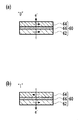
- the magnetic recording medium according to the second embodiment includes a nonmagnetic substrate and a magnetic recording layer, and the magnetic recording layer includes at least one magnetic thin film according to the first embodiment.
- the magnetic recording medium includes a nonmagnetic substrate 10, a magnetic recording layer 30, and an optionally provided seed layer 20.
- the nonmagnetic substrate 10 may be various substrates having a smooth surface. Materials generally used for magnetic recording media can be used.
- the nonmagnetic substrate 10 can be formed using Al alloy plated with NiP, tempered glass, crystallized glass, MgO, or the like.
- the magnetic recording layer 30 may be a single layer or a laminate of a plurality of layers. In the case of a single layer, the magnetic recording layer 30 is the magnetic thin film of the first embodiment.
- the magnetic recording layer is composed of a plurality of layers
- at least one of the plurality of layers is the magnetic thin film of the first embodiment.
- the other layers of the plurality of layers are a layer intended for Curie temperature (Tc) control, a cap layer for adjusting magnetization reversal, an exchange coupling control layer for controlling exchange coupling between two magnetic layers, and magnetic characteristics It may be a magnetic layer for controlling the magnetic field, a magnetic layer for controlling the ferromagnetic resonance frequency for microwave-assisted magnetic recording, or the like. These layers can be formed using any method known in the art, including sputtering.
- the magnetic recording medium of this embodiment is one selected from the group consisting of an adhesion layer, a heat sink layer, a soft magnetic backing layer, an underlayer, and a seed layer 20 between the nonmagnetic substrate 10 and the magnetic recording layer 30. Alternatively, a plurality of layers may be further included.
- the magnetic recording medium of this embodiment may further include a protective layer 40 on the magnetic recording layer 30.
- the magnetic recording medium of this embodiment may further include a liquid lubricant layer on the magnetic recording layer 30 or the protective layer 40.
- the adhesion layer that may be optionally provided is used to enhance the adhesion between the layer formed thereon and the layer (including the nonmagnetic substrate 10) formed thereunder.
- the adhesion layer 20 can be formed using a material having good adhesion to the material of the nonmagnetic substrate 10 described above. Such materials include metals such as Ni, W, Ta, Cr, Ru, and alloys containing the aforementioned metals.
- an adhesion layer may be formed between two constituent layers other than the nonmagnetic substrate 10.
- the adhesion layer may be a single layer or may have a laminated structure of a plurality of layers.
- the soft magnetic backing layer which may be optionally provided controls the magnetic flux from the magnetic head and improves the recording / reproducing characteristics of the magnetic recording medium.
- the materials for forming the soft magnetic underlayer include crystalline materials such as NiFe alloy, sendust (FeSiAl) alloy, CoFe alloy, microcrystalline materials such as FeTaC, CoFeNi, CoNiP, and Co alloys such as CoZrNb and CoTaZr. Including amorphous material.
- the optimum value of the thickness of the soft magnetic underlayer depends on the structure and characteristics of the magnetic head used for magnetic recording. When the soft magnetic backing layer is formed by continuous film formation with other layers, it is preferable that the soft magnetic backing layer has a thickness in the range of 10 nm to 500 nm (including both ends) from the viewpoint of productivity.
- a heat sink layer may be provided.
- the heat sink layer is a layer for effectively absorbing excess heat of the magnetic recording layer 30 generated during the heat-assisted magnetic recording.
- the heat sink layer can be formed using a material having high thermal conductivity and specific heat capacity.
- a material includes Cu simple substance, Ag simple substance, Au simple substance, or an alloy material mainly composed of them.
- “mainly” means that the content of the material is 50 wt% or more.
- the heat sink layer can be formed using an Al—Si alloy, a Cu—B alloy, or the like.
- the heat sink layer can be formed using Sendust (FeSiAl) alloy, soft magnetic CoFe alloy, or the like.
- Sendust FeSiAl
- soft magnetic material By using a soft magnetic material, the function of concentrating the perpendicular magnetic field generated by the head on the magnetic recording layer 30 can be imparted to the heat sink layer, and the function of the soft magnetic backing layer can be supplemented.
- the optimum value of the heat sink layer thickness varies depending on the amount of heat and heat distribution during heat-assisted magnetic recording, the layer configuration of the magnetic recording medium, and the thickness of each component layer. In the case of forming by continuous film formation with other constituent layers, the film thickness of the heat sink layer is preferably 10 nm or more and 100 nm or less in consideration of productivity.
- the heat sink layer can be formed using any method known in the art, such as a sputtering method or a vacuum evaporation method. Usually, the heat sink layer is formed using a sputtering method.
- the heat sink layer can be provided between the nonmagnetic substrate 10 and the adhesion layer, between the adhesion layer and the underlayer, etc. in consideration of characteristics required for the magnetic recording medium.
- the underlayer is a layer for controlling the crystallinity and / or crystal orientation of the seed layer 20 formed above.
- the underlayer may be a single layer or a multilayer.
- the underlayer is formed of Cr metal or an alloy in which at least one metal selected from the group consisting of Mo, W, Ti, V, Mn, Ta, and Zr is added to Cr as a main component.
- a magnetic film is preferred.
- the underlayer can be formed using any method known in the art such as sputtering.
- the function of the seed layer 20 is to ensure the adhesion between the magnetic recording layer 30 and an underlying layer such as an underlayer, and to change the grain size and crystal orientation of the magnetic recording layer 30 of the upper magnetic recording layer 30. Is to control.
- the seed layer 20 is preferably nonmagnetic.
- the temperature rise and temperature distribution of the magnetic recording layer 30 are controlled by using the seed layer 20 as a thermal barrier.
- the seed layer 20 has a function of rapidly raising the temperature of the magnetic recording layer 30 when the magnetic recording layer 30 is heated during the heat-assisted recording, Before the heat transfer in the in-plane direction of the recording layer 30 occurs, it is preferable to achieve both the function of guiding the heat of the magnetic recording layer 30 to the lower layer such as the underlayer by the heat transfer in the depth direction.
- the material of the seed layer 20 is appropriately selected according to the material of the magnetic recording layer 30. More specifically, the material of the seed layer 20 is selected according to the material of the magnetic crystal grains of the magnetic recording layer. For example, if the magnetic crystal grains in the magnetic recording layer 30 is formed by L1 0 type ordered alloy, it is preferable to form the seed layer using a Pt metal or NaCl-type compounds. Particularly preferably, the seed layer 20 is formed using an oxide such as MgO or SrTiO 3 or a nitride such as TiN. Alternatively, the seed layer 20 can be formed by stacking a plurality of layers made of the above materials.
- the seed layer 20 may have a thickness of 1 nm to 60 nm, preferably 1 nm to 20 nm.
- the seed layer 20 can be formed using any method known in the art, such as a sputtering method or a vacuum evaporation method.
- the protective layer can be formed using a material conventionally used in the field of magnetic recording media.
- the protective layer 40 can be formed using a non-magnetic metal such as Pt, a carbon-based material such as diamond-like carbon, or a silicon-based material such as silicon nitride.
- the protective layer may be a single layer or may have a laminated structure.
- the protective layer having a laminated structure may be, for example, a laminated structure of two types of carbon materials having different characteristics, a laminated structure of metals and carbon materials, or a laminated structure of metal oxide films and carbon materials.
- the protective layer can be formed using any method known in the art, such as sputtering, CVD, and vacuum deposition.
- the liquid lubricant layer can be formed using a material conventionally used in the field of magnetic recording media.
- a perfluoropolyether lubricant can be used.
- the liquid lubricant layer can be formed using, for example, a coating method such as a dip coating method or a spin coating method.
- TMR tunnel magnetoresistive element
- the TMR includes a pinned magnetic layer 62, a free magnetic layer 64, and a barrier layer 66 between the pinned magnetic layer 62 and the free magnetic layer 64, as shown in FIG. At least one of 64 is the magnetic thin film of the first embodiment.
- the free magnetic layer 64 is a magnetic layer that can change the direction of magnetization. Magnetization can be changed by a spin injection type using a current flowing through the tunnel magnetoresistive element 60. Or you may change magnetization by the magnetic field given from the outside.
- the barrier layer 66 is a component that disposes a barrier for allowing a tunnel current to flow between the free magnetic layer 64 and the pinned magnetic film 62.
- the barrier layer 66 can be formed using a thin film of an oxide such as magnesium oxide (MgO) or aluminum oxide (Al 2 O 3 ).
- the barrier layer 66 can be formed using any method and conditions known in the art, such as sputtering and vacuum deposition.
- the pinned magnetic film 62 is a component arranged as a magnetic layer whose magnetization direction does not change even when a current or an external magnetic field is applied to the tunnel magnetoresistive element 60.
- the magnitude of the tunnel current flowing through the barrier layer 66 can be changed by the difference in magnetization direction between the fixed magnetic layer 62 and the free magnetic layer 64.
- the tunnel magnetoresistive element 60 having such a configuration operates by changing the magnetization direction of the free magnetic layer 64 by a current supplied to the element or an external magnetic field.
- a tunnel magnetoresistive element that performs spin injection by energization and changes magnetization by spin injection operates as follows. As shown in FIG. 2A, by passing a current from the pinned magnetic layer 62 toward the free magnetic layer 64, the magnetization directions of the pinned magnetic layer 62 and the free magnetic layer 64 can be made parallel. . Further, as shown in FIG. 2B, by passing a current from the free magnetic layer 64 toward the pinned magnetic layer 62, the magnetization directions of the pinned magnetic layer 62 and the free magnetic layer 64 are made antiparallel. be able to.
- Both states shown in FIGS. 2A and 2B can be reversibly changed with each other.
- the tunnel magnetoresistive element 60 can record “0” and “1” information depending on whether the magnetization directions of the pinned magnetic layer 62 and the free magnetic layer 64 are parallel or antiparallel.
- 2A and 2B the case where the magnetization directions of the pinned magnetic layer 62 and the free magnetic layer 64 are parallel is “0”, and the magnetization directions of the pinned magnetic layer 62 and the free magnetic layer 64 are the same.
- “1” is set when “A” is antiparallel, this correspondence may be reversed.
- 2A and 2B exemplify the case where the magnetization directions of the pinned magnetic layer 62 and the free magnetic layer 64 are parallel to the layers.
- the direction of magnetization of the layer 64 may be a direction perpendicular to the layer. Also in this case, information of “0” and “1” is recorded by changing the magnitude of the tunnel current flowing through the barrier layer 66 depending on whether the magnetization directions of both layers are parallel or antiparallel. be able to.
- a magnetoresistive element in which the fixed magnetic layer 62 and the free magnetic layer 64 are directly joined may be used.
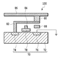
- FIG. 3 shows one configuration example of a magnetic random access memory (MRAM) according to the fourth embodiment.
- FIG. 3 shows a configuration example in which a signal recorded in the TMR is changed by a magnetic field applied from the outside.
- the MRAM 100 shown in FIG. 3 is connected to a MOS-FET 70 having a substrate 72, a source 74, a drain 76, and a gate 78, a tunnel magnetoresistive element 60 connected to the source 74 via a contact 82, and a gate 78.
- Word line 84, bit line 86 connected to tunneling magneto-resistance element 60, and digit line 88 for applying a write magnetic field to tunneling magneto-resistance element 60 are included.
- the MRAM 100 causes a current to flow through the bit line 86 and the digit line 88 and records a signal of “0” or “1” in the tunnel magnetoresistive element 60 by the resultant combined magnetic field.
- the bit line 86 and the digit line 88 extend in a direction crossing each other, and a signal can be recorded in the tunnel magnetoresistive element 60 located at the intersection of the bit line 86 and the digit line 88 through which a current flows.
- the signal from the MRAM 100 applies a current to the word line 84 to apply a voltage to the bit line 86 in a state where the MOS-FET 70 is turned “ON”. It can be read out by detecting the current flowing to the MOS-FET 70 via the contact 82.
- the current at this time corresponds to the tunnel current of the tunnel magnetoresistive element 60 and corresponds to a signal of “0” or “1”.
- a method other than the configuration example of FIG. 3 may be used. For example, a spin-injection type magnetoresistive element may be used, and a signal to be recorded may be changed by a current flowing through the magnetoresistive element.
- the magnetic thin film of the first embodiment can be used in a MEMS device.
- the MEMS device can be formed using any known technique by incorporating the magnetic thin film of the first embodiment into a predetermined member.
- Example 1 A (001) MgO single crystal substrate (manufactured by Tateho Chemical Industry Co., Ltd.) having a smooth surface was washed to prepare a nonmagnetic substrate 10.
- the nonmagnetic substrate 10 after cleaning was introduced into the sputtering apparatus. After heating the nonmagnetic substrate 10 to 350 ° C., a 20 nm-thick Pt seed layer 20 was formed by RF magnetron sputtering using a Pt target in Ar gas at a pressure of 0.4 Pa.
- an FePtSc magnetic film having a thickness of 10 nm is formed by an RF magnetron sputtering method using an FePt target and an Sc target in Ar gas at a pressure of 0.6 Pa.
- a recording layer 30 was formed to obtain a magnetic recording medium having the structure shown in FIG.
- a target having a Fe / Pt ratio of 45/55 was used as the FePt target.
- the electric power applied to the FePt target was fixed at 300 W, and the electric power applied to the Sc target was changed from 40 to 450 W to adjust the Sc content in the magnetic recording layer 30.
- magnetic recording layer 30 of the resultant magnetic recording medium is determined to have a L1 0 ordered structure. Further, by XRD, to determine the length of a-axis and c-axis of the crystal lattice of the L1 0 ordered structure. Furthermore, using a vibrating sample magnetometer (VSM), the hysteresis curve of the obtained magnetic recording medium was measured, and the coercive force Hc was measured. Further, the composition of the magnetic recording layer 30 of the obtained magnetic recording medium was measured by Rutherford backscattering method (RBS). The above measurement results are shown in Table 1.
- VSM vibrating sample magnetometer
- RBS Rutherford backscattering method
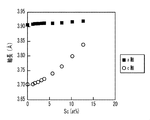
- FIG. 4 shows the relationship between the Sc content of the magnetic recording layer 30 and the lengths of the a-axis and c-axis of the crystal lattice.
- the length of the a-axis of the crystal lattice hardly changes.
- the length of the c-axis of the crystal lattice increases as the Sc content increases. From this, it is considered that Sc exists in the FePt crystal grains.
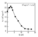
- FIG. 5 shows the relationship between the Sc content of the magnetic recording layer 30 and the coercive force Hc.
- FIG. 6 shows the relationship between the Sc content of the magnetic recording layer 30 and the magnetic anisotropy constant Ku.
- the inclusion of Sc increases the coercivity Hc and the magnetic anisotropy constant Ku.
- the coercive force Hc shows a maximum value of 8.5 kOe (680 A / mm)
- the magnetic anisotropy constant Ku is 26.7 erg / cm 3 ( The maximum value of 2.67 J / m 3 ) was shown.
Landscapes
- Engineering & Computer Science (AREA)
- Computer Hardware Design (AREA)
- Microelectronics & Electronic Packaging (AREA)
- Crystallography & Structural Chemistry (AREA)
- Power Engineering (AREA)
- Chemical & Material Sciences (AREA)
- Spectroscopy & Molecular Physics (AREA)
- Physics & Mathematics (AREA)
- Manufacturing & Machinery (AREA)
- Thin Magnetic Films (AREA)
- Hall/Mr Elements (AREA)
- Mram Or Spin Memory Techniques (AREA)
- Magnetic Record Carriers (AREA)
- Micromachines (AREA)
- Magnetic Heads (AREA)
Abstract
本発明の課題は、高い磁気異方性定数Kuおよび大きな保磁力Hcを有する磁性薄膜、および当該磁性薄膜を含む応用デバイスを提供することである。本発明の磁性薄膜は、FeおよびNiからなる群から選択される少なくとも1種の第1元素と、Pt、Pd、AuおよびIrからなる群から選択される少なくとも1種の第2元素と、Scとを含む規則合金を含む。
Description
本明細書に実施形態のいくつかが開示される発明は、規則合金を含む磁性薄膜に関する。より詳細には、実施形態の構成例のいくつかは、規則合金が、FeおよびPtを主成分とし、Scを含む、磁性薄膜に関する。さらに、本明細書に実施形態のいくつかが開示される発明は、前述の磁性薄膜を含む応用デバイスに関する。
磁性薄膜を含む応用デバイスは、磁気記録媒体、トンネル磁気抵抗素子(TMR)、磁気抵抗ランダムアクセスメモリ(MRAM)、およびマイクロエレクトロメカニカルシステム(MEMS)デバイスなどを含む。
磁性薄膜を含む応用デバイスの第1の例として、磁気記録媒体を説明する。磁気記録媒体は、ハードディスク、光磁気記録(MO)ディスク、および磁気テープなどの磁気記録装置に用いられている。その磁気記録方式は、面内磁気記録方式および垂直磁気記録方式を含む。
面内磁気記録方式は、従来用いられてきた方式であって、たとえばハードディスク表面に対して水平に磁気記録を行う方式である。しかしながら、近年では、より高い記録密度を実現可能な、ディスク表面に対して垂直に磁気記録を行う垂直磁気記録方式が主に用いられている。
垂直磁気記録方式に用いられる磁気記録媒体(以下、「垂直磁気記録媒体」と記載する場合がある)は、非磁性基板と、硬質磁性材料から形成される磁気記録層を少なくとも含む。垂直磁気記録媒体は、任意選択的に、軟磁性材料から形成されて、磁気ヘッドが発生する磁束を磁気記録層に集中させる役割を担う軟磁性裏打ち層、磁気記録層の硬質磁性材料を目的の方向に配向させるためのシード層、磁気記録層の表面を保護する保護層などをさらに含んでもよい。
近年、垂直磁気記録媒体の記録密度のさらなる向上を目的として、磁気記録層中の磁性結晶粒の粒径を縮小させる必要に迫られている。一方で、磁性結晶粒の粒径の縮小は、記録された磁化の熱安定性を低下させる。そのため、磁性結晶粒の粒径の縮小による熱安定性の低下を補償するために、磁性結晶粒を、より高い結晶磁気異方性を有する材料を用いて形成することが求められている。
しかしながら、高い磁気異方性を有する材料で形成された磁気記録層を有する磁気記録媒体は、大きな保磁力を有し、磁化の記録が困難である。この記録困難性を克服するために、熱アシスト記録方式、マイクロ波アシスト記録方式などのエネルギーアシスト磁気記録方式が提案されている。熱アシスト記録方式は、磁性材料における磁気異方性定数(Ku)の温度依存性、すなわち高温ほどKuが小さいという特性を利用したものである。この方式では、磁気記録層の加熱機能を有するヘッドを用いる。すなわち、磁気記録層を昇温させて一時的にKuを低下させることにより反転磁界を低減させ、その間に書き込みを行う。降温後はKuが元の高い値に戻るため、安定して記録した磁化を保持できる。
磁性薄膜を含む応用デバイスの第2の例として、トンネル磁気抵抗素子(TMR)、およびこれを用いた磁気抵抗ランダムアクセスメモリ(MRAM)を説明する。フラッシュメモリ、スタティックランダムアクセスメモリ(SRAM)、ダイナミックランダムアクセスメモリ(DRAM)などの従来のメモリは、メモリセル内の電子を用いて情報の記録を行っている。一方、MRAMは、記録媒体にハードディスクなどと同じ磁性体を用いたメモリである。
MRAMは、10ns程度のアドレスアクセスタイム、および20ns程度のサイクルタイムを有する。このため、MRAMの読み書き速度は、DRAMの読み書き速度の5倍程度であり、すなわち、スタティックランダムアクセスメモリ(SRAM)の読み書き速度と同等である。また、MRAMは、フラッシュメモリの10分の1程度の低消費電力、ならびに高密度の集積を実現できるという利点を有する。
ここで、MRAMに用いるTMRは、種々の技術によって製造することができる。たとえば、反強磁性薄膜上に強磁性薄膜を形成することによって、TMRを含む積層体を得ることができる。特開2005-333106号公報(特許文献1)は、基板上に、反強磁性層、および該反強磁性層と交換結合する強磁性層が順次積層され、上記反強磁性層が、Mn-Ir合金の規則相(Mn3Ir)を含む交換結合素子を開示している。当該文献の図5には、前述の交換結合素子を含むTMRの模式断面図が開示されている。また、当該文献の図4には、交換結合素子を具備したスピンバルブ型磁気抵抗素子が開示されている。
磁性薄膜を含む応用デバイスの第3の例として、マイクロエレクトロメカニカルシステム(MEMS)デバイスを説明する。MEMSデバイスとは、機械要素部品、センサー、アクチュエータ、および/または電子回路を単一の基板の上に集積化したデバイスの総称である。用いることができる基板は、シリコン基板、ガラス基板、または有機材料基板を含む。MEMSデバイスの応用例は:プロジェクタの光学素子の1種であるデジタルマイクロミラーデバイス(DMD);インクジェットプリンタのヘッド部に用いる微小ノズル;ならびに、圧力センサー、加速度センサー、および流量センサーのような各種のセンサーを含む。近年では、製造業における応用に加えて、医療分野などにおけるMEMSデバイスの応用が期待されている。
前述の応用デバイス(磁気記録媒体、TMR、MRAM、及びMEMSデバイス)のいずれにおいても、磁性薄膜の磁気特性の向上、具体的には一軸磁気異方性定数(Ku)の向上が要請されている。なお、このように優れたKu値を示す磁性薄膜の開発は、今後、記録媒体およびメモリの大容量化および/または高密度化に多大に貢献すると考えられる。
優れたKu値を示す材料の候補として規則合金が注目され、その研究が活発に行われている。規則合金としては、FePt、CoPt等の各種の材料が着目されている。これらに添加して特性を向上するための添加材料の探索も続けられている。この点に関して、特開2010-135610号公報(特許文献2)は、L11型のCo-Pt-C規則合金を含有する磁性薄膜を提案している。このCo-Pt-C規則合金は、任意選択的に、Ni、Fe、Mn、Cr、V、Ti、Sc、Cu、Zn、Pd、Rh、Ru、Mo、Nb、Zr、Ag、Ir、Au、Re、W、Ta、Hf、Al、Si、Ge、およびBからなる群から選択される少なくとも1種の添加元素を含むことができる。しかしながら、これらの添加元素が磁性薄膜に与える影響は、具体的には検討されていない。
また、特開2008-59733号公報(特許文献3)は、FePd、FePt、CoPtおよびMnAlのようなL10型規則合金からなる磁性結晶粒と、酸化物からなる非磁性結晶粒界とで構成されるグラニュラー構造の磁気記録層を有する磁気記録媒体を提案している。ここで、酸化物は、酸素と、少なくとも1つの元素が負の還元電位を有する1つまたは複数の元素とから構成される。酸化物を構成する元素の例として、スカンジウム(Sc)が記載されている。しかしながら、当該文献は、上記のグラニュラー構造の磁気記録層の特性について何らの評価も行っていない。加えて、当該文献は、L10型規則合金に添加元素を導入することを開示も示唆もしていない。
以上のように、規則合金に添加する材料としてのScに関する研究はほとんど進んでいないのが現状である。Scを添加した場合の規則合金の磁気特性、特に、そのような規則合金における磁気異方性定数Kuについての研究はほとんど進展していない。
本明細書に構成例のいくつかが開示される発明の目的は、高い磁気異方性定数Kuおよび大きな保磁力Hcを有する磁性薄膜、および当該磁性薄膜を含む応用デバイスを提供することである。
本発明の実施形態の1つの例である磁性薄膜は、規則合金を含み、前記規則合金は、FeおよびNiからなる群から選択される少なくとも1種の第1元素と、Pt、Pd、AuおよびIrからなる群から選択される少なくとも1種の第2元素と、Scとを含むことを特徴とする。好ましくは、第1元素がFeであり、第2元素がPtである。また、規則合金は、L10型規則構造を有することが望ましい。また、本実施形態の磁性薄膜は、前述の規則合金を含む磁性結晶粒と、非磁性結晶粒界とからなるグラニュラー構造を有してもよい。非磁性結晶粒界は、炭素、ホウ素、酸化物および窒化物からなる群から選択される少なくとも1つの材料を含むことができる。また、本実施形態の磁性薄膜を用いて、マイクロエレクトロメカニカルシステムを形成することができる。
本発明の実施形態の1つの例である磁気記録媒体は、非磁性基板と磁気記録層とを含み、前記磁気記録層が前記磁性薄膜を含むことを特徴とする。
本発明の実施形態の1つの例であるトンネル磁気抵抗素子は、固定磁性層と、自由磁性層と、障壁層とを含み、前記障壁層は、前記固定磁性層と前記自由磁性層との間に位置し、前記固定磁性層および前記自由磁性層の少なくとも一方は、前記磁性薄膜を含むことを特徴とする。このトンネル磁気抵抗素子を用いて、磁気ランダムアクセスメモリを形成することができる。
上記の構成を採用することによって、本発明の実施形態の1つの例である磁性薄膜は、大きな磁気異方性定数Kuおよび大きな保磁力Hcの両方を有することが可能となる。また、前述の特性を有する磁性薄膜は、高い記録密度を有する磁気記録媒体の磁気記録層として有用である。さらに、上記の磁性薄膜は、磁気抵抗素子の小型化、磁気ランダムアクセスメモリおよびマイクロエレクトロメカニカルシステムの集積度の向上などにも有用であると考えられる。
第1の実施形態の磁性薄膜は、規則合金を含み、前記規則合金は、FeおよびNiからなる群から選択される少なくとも1種の第1元素と、Pt、Pd、AuおよびIrからなる群から選択される少なくとも1種の第2元素と、Scとを含む。好ましくは、規則合金は、L10型構造を有する。好ましいL10型規則合金は、FePtSc、およびFePdScを含む。また、特に好ましいL10型規則合金は、第1元素としてのFe、第2元素としてのPt、およびScを含む。
本実施形態に用いられる規則合金において、第2元素に対する第1元素の比は、原子数を基準として0.7~1.3の範囲内、好ましくは0.8~1.1の範囲内としてもよい。この範囲内の組成比を用いることによって、大きな磁気異方性定数Kuを有するL10型規則構造を得ることができる。
本実施形態に用いられる規則合金中のScは、好ましくは、0価の酸化状態のSc、すなわち金属状態のScである。何らかの理論に拘束されることを意図するものではないが、Scの添加によりL10型規則構造の結晶格子のc軸長が増大する変形が生じ、この結晶格子の変形によって大きな磁気異方性定数Kuおよび大きな保磁力Hcが得られると考えることができる。規則合金は、Sc酸化物のようなより高い酸化状態のScを含まない。より高い酸化状態のScの化合物による他原子の置換、あるいは、より高い酸化状態のScの化合物の格子内への侵入などの結晶格子を変形させる過程は原理的に起こりにくいと考えられるため、より高い酸化状態のScの化合物によって本実施形態の作用効果が実現できるとは考えにくいためである。
本実施形態において、規則合金は、必ずしもすべての原子が規則構造を有していなくてもよい。規則構造の程度を表わす規則度Sが所定の値以上であれば良い。規則度Sは、磁性薄膜をX線回折法(XRD)により測定し、測定値と完全に規則化した際の理論値との比により算出される。L10型規則合金の場合は、規則合金由来の(001)および(002)ピークの積分強度を用いて算出する。測定された(001)ピーク積分強度に対する(002)ピーク積分強度の比の値を、完全に規則化した際に理論的に算出される(001)ピーク積分強度に対する(002)ピーク積分強度の比で除算することで規則度Sを得ることができる。このようにして得られた規則度Sが0.5以上であれば、磁性薄膜として実用的な磁気異方性定数Kuを有する。
本実施形態の磁性薄膜は、前記規則合金からなる磁性結晶粒と、非磁性結晶粒界とからなるグラニュラー構造を有してもよい。ここで、非磁性結晶粒界は、炭素(C)、ホウ素(B)、酸化物、および窒化物を含んでもよい。非磁性結晶粒界に用いることができる酸化物は、SiO2、TiO2、およびZnOを含む。非磁性結晶粒界に用いることができる窒化物は、SiNおよびTiNを含む。グラニュラー構造において、それぞれの磁性結晶粒は、非磁性結晶粒界によって磁気的に分離される。この磁気的分離は、特に、磁性薄膜を磁気記録媒体の磁気記録層に用いた場合に、磁気記録媒体のSNR向上に有効である。
本実施形態の磁性薄膜は、好ましくは、基板の加熱を伴うスパッタ法にて形成される。スパッタ法としては、DCマグネトロンスパッタリング法、RFスパッタリング法などの当該技術分野においてよく知られた方法を用いることができる。以下の説明でスパッタ法と記載する場合も特に断りがない限り同様である。磁性薄膜を形成する際の基板温度は、400~500℃の範囲内であることが好ましい。この範囲内の基板温度を採用することにより、磁性薄膜中のL10型規則合金材料の規則度Sを向上させることができる。スパッタ法に用いるターゲットとして、第1元素および第2元素からなるターゲット、およびScからなるターゲットである2つのターゲットを用いてもよい。あるいはまた、第1元素からなるターゲット、第2元素からなるターゲット、およびScからなるターゲットである3つのターゲットを用いてもよい。これらの場合、それぞれのターゲットに別個に電力を供給することによって、磁気記録層30の規則合金中の第1元素、第2元素およびScの比率を制御することができる。
本実施形態の磁性薄膜の形成に用いられる基板は、表面が平滑である様々な基板であってもよい。たとえば、NiPメッキを施したAl合金、強化ガラス、結晶化ガラス、シリコンまたはMgOなどを、基板として用いることができる。
グラニュラー構造を有する磁性薄膜の形成の際には、磁性結晶粒を形成する材料と非磁性結晶粒界を形成する材料を所定の比率で混合したターゲットを用いてもよい。あるいはまた、磁性結晶粒を形成する材料からなるターゲットと、非磁性結晶粒界を形成する材料からなるターゲットとを用いてもよい。前述のように、磁性結晶粒を形成するためのターゲットとして複数のターゲットを用いてもよい。この場合、それぞれのターゲットに別個に電力を供給して、磁性薄膜中の磁性結晶粒と非磁性結晶粒界との比率を制御することができる。
第2の実施形態の磁気記録媒体は、非磁性基板と磁気記録層とを含み、前記磁気記録層は、少なくとも1つの第1の実施形態の磁性薄膜を含む。たとえば、図1に示す構成例では、磁気記録媒体は非磁性基板10、磁気記録層30、および任意選択的に設けてもよいシード層20を含む。
非磁性基板10は、表面が平滑である様々な基板であってもよい。磁気記録媒体に一般的に用いられる材料を用いることができる。たとえば、NiPメッキを施したAl合金、強化ガラス、結晶化ガラス、あるいはMgO等を用いて、非磁性基板10を形成することができる。
磁気記録層30は、単一の層であっても、複数の層の積層体であってもよい。単一の層で構成される場合、磁気記録層30は、第1の実施形態の磁性薄膜である。
磁気記録層が複数の層から構成される場合、複数の層の少なくとも1つは、第1の実施形態の磁性薄膜である。複数の層のその他の層は、キュリー温度(Tc)制御を目的とする層、磁化反転を調整するためのキャップ層、2つの磁性層間の交換結合を制御するための交換結合制御層、磁気特性を制御するための磁性層、マイクロ波アシスト磁気記録に向けた強磁性共鳴周波数を制御する磁性層などであってもよい。これらの層は、スパッタ法を含む、当該技術において知られている任意の方法を用いて形成することができる。
本実施形態の磁気記録媒体は、非磁性基板10と磁気記録層30との間に、密着層、ヒートシンク層、軟磁性裏打ち層、下地層、およびシード層20からなる群から選択される1つまたは複数の層をさらに含んでもよい。また、本実施形態の磁気記録媒体は、磁気記録層30の上に保護層40をさらに含んでもよい。さらに、本実施形態の磁気記録媒体は、磁気記録層30または保護層40の上に液体潤滑剤層をさらに含んでもよい。
任意選択的に設けてもよい密着層は、その上に形成される層とその下に形成される層(非磁性基板10を含む)との密着性を高めるために用いられる。密着層を非磁性基板10の上面に設ける場合、密着層20は、前述の非磁性基板10の材料との密着性が良好な材料を用いて形成することができる。そのような材料は、Ni、W、Ta、Cr、Ruなどの金属、前述の金属を含む合金を含む。あるいはまた、非磁性基板10以外の2つの構成層の間に密着層を形成してもよい。密着層は、単一の層であってもよいし、複数の層の積層構造を有してもよい。
任意選択的に設けてもよい軟磁性裏打ち層は、磁気ヘッドからの磁束を制御して、磁気記録媒体の記録・再生特性を向上させる。軟磁性裏打ち層を形成するための材料は、NiFe合金、センダスト(FeSiAl)合金、CoFe合金などの結晶質材料、FeTaC,CoFeNi,CoNiPなどの微結晶質材料、および、CoZrNb、CoTaZrなどのCo合金を含む非晶質材料を含む。軟磁性裏打ち層の膜厚の最適値は、磁気記録に用いる磁気ヘッドの構造および特性に依存する。他の層と連続成膜で軟磁性裏打ち層を形成する場合、生産性との兼ね合いから、軟磁性裏打ち層が10nm~500nmの範囲内(両端を含む)の膜厚を有することが好ましい。
本実施形態の磁気記録媒体を熱アシスト磁気記録方式において使用する場合、ヒートシンク層を設けてもよい。ヒートシンク層は、熱アシスト磁気記録時に発生する磁気記録層30の余分な熱を効果的に吸収するための層である。ヒートシンク層は、熱伝導率および比熱容量が高い材料を用いて形成することができる。そのような材料は、Cu単体、Ag単体、Au単体、またはそれらを主体とする合金材料を含む。ここで、「主体とする」とは、当該材料の含有量が50wt%以上であることを示す。また、強度などの観点から、Al-Si合金、Cu-B合金などを用いて、ヒートシンク層を形成することができる。さらに、センダスト(FeSiAl)合金、軟磁性のCoFe合金などを用いてヒートシンク層を形成することができる。軟磁性材料を用いることによって、ヘッドの発生する垂直方向磁界を磁気記録層30に集中させる機能をヒートシンク層に付与することができ、軟磁性裏打ち層の機能を補完することもできる。ヒートシンク層の膜厚の最適値は、熱アシスト磁気記録時の熱量および熱分布、ならびに磁気記録媒体の層構成および各構成層の厚さによって変化する。他の構成層との連続成膜で形成する場合などは、生産性との兼ね合いから、ヒートシンク層の膜厚は10nm以上100nm以下であることが好ましい。ヒートシンク層は、スパッタ法、真空蒸着法などの当該技術において知られている任意の方法を用いて形成することができる。通常の場合、ヒートシンク層は、スパッタ法を用いて形成される。ヒートシンク層は、磁気記録媒体に求められる特性を考慮して、非磁性基板10と密着層との間、密着層と下地層との間などに設けることができる。
下地層は、上方に形成されるシード層20の結晶性および/または結晶配向を制御するための層である。下地層は単層であっても多層であってもよい。下地層は、Cr金属、または主成分であるCrにMo、W、Ti、V、Mn、Ta、およびZrからなる群から選択される少なくとも1種の金属が添加された合金から形成される非磁性膜であることが好ましい。下地層は、スパッタ法などの当該技術において知られている任意の方法を用いて形成することができる。
シード層20の機能は、下地層などのその下にある層と磁気記録層30との間の密着性を確保すること、上層である磁気記録層30の磁性結晶粒の粒径および結晶配向を制御することである。シード層20は非磁性であることが好ましい。加えて、本実施形態の磁気記録媒体を熱アシスト磁気記録方式において使用する場合には、シード層20が熱的なバリアとして磁気記録層30の温度上昇および温度分布を制御することが好ましい。磁気記録層30の温度上昇および温度分布を制御するために、シード層20は、熱アシスト記録時の磁気記録層30の加熱の際に磁気記録層30の温度を速やかに上昇させる機能と、磁気記録層30の面内方向の伝熱が起こる前に、深さ方向の伝熱によって磁気記録層30の熱を下地層などの下層に導く機能とを両立することが好ましい。
上記の機能を達成するために、シード層20の材料は、磁気記録層30の材料に合わせて適宜選択される。より具体的には、シード層20の材料は、磁気記録層の磁性結晶粒の材料に合わせて選択される。たとえば、磁気記録層30の磁性結晶粒がL10型規則合金で形成される場合、Pt金属、またはNaCl型の化合物を用いてシード層を形成することが好ましい。特に好ましくは、MgO、SrTiO3などの酸化物、あるいはTiNなどの窒化物を用いてシード層20を形成する。また、上記の材料からなる複数の層を積層して、シード層20を形成することもできる。磁気記録層30の磁性結晶粒の結晶性の向上、および生産性の向上の観点から、シード層20は、1nm~60nm、好ましくは1nm~20nmの膜厚を有してもよい。シード層20は、スパッタ法、真空蒸着法などの当該技術において知られている任意の方法を用いて形成することができる。
保護層は、磁気記録媒体の分野で慣用的に使用されている材料を用いて形成することができる。具体的には、Ptなどの非磁性金属、ダイアモンドライクカーボンなどのカーボン系材料、あるいは窒化シリコンなどのシリコン系材料を用いて、保護層40を形成することができる。また、保護層は、単層であってもよく、積層構造を有してもよい。積層構造の保護層は、たとえば、特性の異なる2種のカーボン系材料の積層構造、金属とカーボン系材料との積層構造、または金属酸化物膜とカーボン系材料との積層構造であってもよい。保護層は、スパッタ法、CVD法、真空蒸着法などの当該技術において知られている任意の方法を用いて形成することができる。
液体潤滑剤層は、磁気記録媒体の分野で慣用的に使用されている材料を用いて形成することができる。たとえば、パーフルオロポリエーテル系の潤滑剤などを用いることができる。液体潤滑剤層は、たとえば、ディップコート法、スピンコート法などの塗布法を用いて形成することができる。
第3の実施形態である磁気抵抗素子について説明する。以下ではわかりやすさのためにトンネル磁気抵抗素子(TMR)を例にとって説明する。TMRは、図2に示すように、固定磁性層62と、自由磁性層64と、固定磁性層62と自由磁性層64との間の障壁層66とを含み、固定磁性層62および自由磁性層64の少なくとも一方は、第1の実施形態の磁性薄膜である。
自由磁性層64は、磁化の方位を変化することができる磁性層である。トンネル磁気抵抗素子60に流す電流を用いてスピン注入型によって磁化を変化させることができる。あるいは外部から与える磁界によって磁化を変化させてもよい。
障壁層66は、自由磁性層64と固定磁性膜62の間にトンネル電流を流すための障壁を配設する構成要素である。障壁層66は酸化マグネシウム(MgO)、酸化アルミニウム(Al2O3)等の酸化物の薄膜を用いて形成することができる。障壁層66は、たとえば、スパッタ法、真空蒸着法など当該技術において知られている任意の方法及び条件を用いて形成することができる。
固定磁性膜62は、トンネル磁気抵抗素子60に、電流あるいは外部磁界を与えた場合でも、磁化の向きが変化しない磁性層として配設する構成要素である。固定磁性層62と自由磁性層64の磁化の向きの違いにより、障壁層66を流れるトンネル電流の大きさを変化させることができる。
このような構成のトンネル磁気抵抗素子60は、同素子に供給する電流または外部磁界により自由磁性層64の磁化の向きを変化せることで動作する。たとえば、通電によってスピン注入を行い、スピン注入によって磁化を変化させるトンネル型磁気抵抗素子は次のように動作する。図2(a)に示すように、固定磁性層62から自由磁性層64に向かって電流を流すことによって、固定磁性層62および自由磁性層64の磁化の向きが平行な状態とすることができる。また、図2(b)に示すように、自由磁性層64から固定磁性層62に向かって電流を流すことによって、固定磁性層62および自由磁性層64の磁化の向きが反平行な状態とすることができる。図2(a)および図2(b)に示す両状態は、可逆的に相互に変化させることができる。トンネル磁気抵抗素子60は、固定磁性層62および自由磁性層64の磁化の向きが平行であるか反平行であるかによって、「0」および「1」の情報を記録することができる。図2(a)および図2(b)において、固定磁性層62および自由磁性層64の磁化の向きが平行である場合を「0」とし、固定磁性層62および自由磁性層64の磁化の向きが反平行である場合を「1」としたが、この対応関係は逆であってもよい。また、図2(a)および図2(b)において、固定磁性層62および自由磁性層64の磁化の向きが層に平行である方向である場合を例示したが、固定磁性層62および自由磁性層64の磁化の向きは、層に垂直な方向であってもよい。この場合にも、両層の磁化の向きが平行であるか反平行であるかによって、障壁層66を流れるトンネル電流の大きさを変化させて、「0」および「1」の情報を記録することができる。以上説明したTMRの他にも、固定磁性層62と自由磁性層64を直接に接合した磁気抵抗素子としてもよい。
第4の実施形態である磁気ランダムアクセスメモリ(MRAM)の1つの構成例を、図3に示す。図3は、外部から印加する磁界によってTMRに記録する信号を変化させる構成例である。図3に示すMRAM100は、基板72、ソース74、ドレイン76、およびゲート78を有するMOS-FET70と、コンタクト82を介してソース74と接続されるトンネル磁気抵抗素子60と、ゲート78と接続されるワード線84と、トンネル磁気抵抗素子60と接続されるビット線86と、トンネル磁気抵抗素子60に書込み磁界を印加するためのディジット線88とを含む。
本実施形態のMRAM100は、ビット線86およびディジット線88に電流を流し、得られる合成磁界によって、トンネル磁気抵抗素子60に、「0」または「1」の信号を記録する。ビット線86およびディジット線88は、互いに交差する方向に延びており、電流を流したビット線86およびディジット線88の交点に位置するトンネル磁気抵抗素子60に信号を記録することができる。
一方、MRAM100からの信号は、ワード線84に電流を流して、MOS-FET70を「オン」にした状態で、ビット線86に電圧を印加して、ビット線86から、トンネル磁気抵抗素子60およびコンタクト82を介して、MOS-FET70へと流れる電流を検知することによって,読み出すことができる。この際の電流は、トンネル磁気抵抗素子60のトンネル電流に相当し、「0」または「1」の信号に対応する。図3の構成例以外の方法としてもよい。たとえば、スピン注入型の磁気抵抗素子を用い、磁気抵抗素子に通電する電流によって記録する信号を変化させてもよい。
上記の第2~第4の実施形態に加えて、第1の実施形態の磁性薄膜は、MEMSデバイス中で用いることができる。MEMSデバイスは、所定部材に第1の実施形態の磁性薄膜を組み込んで、任意の公知技術を用いて形成することができる。
(実施例1)
平滑な表面を有する(001)MgO単結晶基板(タテホ化学工業株式会社製)を洗浄し、非磁性基板10を準備した。洗浄後の非磁性基板10を、スパッタ装置内に導入した。非磁性基板10を350℃に加熱した後に、圧力0.4PaのArガス中でPtターゲットを用いたRFマグネトロンスパッタ法により、膜厚20nmのPtシード層20を形成した。
平滑な表面を有する(001)MgO単結晶基板(タテホ化学工業株式会社製)を洗浄し、非磁性基板10を準備した。洗浄後の非磁性基板10を、スパッタ装置内に導入した。非磁性基板10を350℃に加熱した後に、圧力0.4PaのArガス中でPtターゲットを用いたRFマグネトロンスパッタ法により、膜厚20nmのPtシード層20を形成した。
次に、シード層20を形成した非磁性基板10を350℃に加熱した後に、圧力0.6PaのArガス中で、FePtターゲットおよびScターゲットを用いるRFマグネトロンスパッタ法により、膜厚10nmのFePtSc磁気記録層30を形成し、図1に示す構造を有する磁気記録媒体を得た。ここで、FePtターゲットとして、Fe/Pt比が45/55のターゲットを用いた。また、FePtターゲットに印加する電力を300Wに固定し、Scターゲットに印加する電力を40~450Wに変化させて、磁気記録層30のScの含有量を調整した。
XRDにより、得られた磁気記録媒体の磁気記録層30がL10型規則構造を有することを確認した。また、XRDにより、L10型規則構造の結晶格子のa軸およびc軸の長さを測定した。さらに、振動試料型磁力計(VSM)を用いて、得られた磁気記録媒体のヒステリシス曲線を測定し、保磁力Hcを測定した。また、得られた磁気記録媒体の磁気記録層30の組成を、ラザフォード後方散乱法(RBS)により測定した。以上の測定結果を第1表に示す。

磁気記録層30のSc含有量と、結晶格子のa軸およびc軸の長さとの関係を図4に示す。図4から分かるように、Sc含有量が増加しても、結晶格子のa軸の長さはほとんど変化しない。一方、結晶格子のc軸の長さは、Sc含有量の増加に伴って増大する。このことから、ScがFePt結晶粒中に存在すると考えられる。
磁気記録層30のSc含有量と、保磁力Hcとの関係を図5に示す。また、磁気記録層30のSc含有量と、磁気異方性定数Kuとの関係を図6に示す。図5および図6から分かるように、Scを含むことにより、保磁力Hcおよび磁気異方性定数Kuが増大する。特に、Scの含有量が2.4at%である場合に、保磁力Hcが8.5kOe(680A/mm)の最大値を示し、かつ、磁気異方性定数Kuが26.7erg/cm3(2.67J/m3)の最大値を示した。
これらのことから、L10型規則合金に対するScの添加が、優れた磁気特性の発現に有効であることが分かる。
10 非磁性基板
20 シード層
30 磁気記録層
60 トンネル磁気抵抗素子
62 固定磁性層
64 自由磁性層
66 障壁層
70 MOS-FET
72 基板
74 ソース
76 ドレイン
78 ゲート
82 コンタクト
84 ワード線
86 ビット線
88 ディジット線
100 MRAM
20 シード層
30 磁気記録層
60 トンネル磁気抵抗素子
62 固定磁性層
64 自由磁性層
66 障壁層
70 MOS-FET
72 基板
74 ソース
76 ドレイン
78 ゲート
82 コンタクト
84 ワード線
86 ビット線
88 ディジット線
100 MRAM
Claims (9)
- 規則合金を含み、前記規則合金は、FeおよびNiからなる群から選択される少なくとも1種の第1元素と、Pt、Pd、AuおよびIrからなる群から選択される少なくとも1種の第2元素と、Scとを含むことを特徴とする磁性薄膜。
- 前記第1元素がFeであり、前記第2元素がPtであることを特徴とする請求項1に記載の磁性薄膜。
- 前記規則合金がL10型規則構造を有することを特徴とする請求項1に記載の磁性薄膜。
- 前記磁性薄膜が、前記規則合金を含む磁性結晶粒と、非磁性結晶粒界とからなるグラニュラー構造を有し、前記非磁性結晶粒界は、炭素、ホウ素、酸化物および窒化物からなる群から選択される少なくとも1つの材料を含むことを特徴とする請求項1に記載の磁性薄膜。
- 非磁性基板と磁気記録層とを含み、前記磁気記録層が請求項1に記載の磁性薄膜を含むことを特徴とする磁気記録媒体。
- 請求項1に記載の磁性薄膜を含むことを特徴とする磁気抵抗素子。
- 固定磁性層と、自由磁性層と、障壁層とを含み、前記障壁層は、前記固定磁性層と前記自由磁性層との間に位置し、前記固定磁性層および前記自由磁性層の少なくとも一方は、請求項1に記載の磁性薄膜を含むことを特徴とするトンネル磁気抵抗素子。
- 請求項6に記載の磁気抵抗素子を含むことを特徴とする磁気ランダムアクセスメモリ。
- 請求項1に記載の磁性薄膜を含むことを特徴とするマイクロエレクトロメカニカルシステム。
Priority Applications (3)
| Application Number | Priority Date | Filing Date | Title |
|---|---|---|---|
| CN201580011466.4A CN106062900B (zh) | 2014-06-24 | 2015-05-19 | 磁性薄膜以及包括磁性薄膜的应用设备 |
| SG11201607105PA SG11201607105PA (en) | 2014-06-24 | 2015-05-19 | Magnetic thin film and application device including magnetic thin film |
| US15/251,056 US10115890B2 (en) | 2014-06-24 | 2016-08-30 | Magnetic thin film and application device including magnetic thin film |
Applications Claiming Priority (2)
| Application Number | Priority Date | Filing Date | Title |
|---|---|---|---|
| JP2014129203A JP6375719B2 (ja) | 2014-06-24 | 2014-06-24 | 磁性薄膜および磁性薄膜を含む応用デバイス |
| JP2014-129203 | 2014-06-24 |
Related Child Applications (1)
| Application Number | Title | Priority Date | Filing Date |
|---|---|---|---|
| US15/251,056 Continuation US10115890B2 (en) | 2014-06-24 | 2016-08-30 | Magnetic thin film and application device including magnetic thin film |
Publications (1)
| Publication Number | Publication Date |
|---|---|
| WO2015198523A1 true WO2015198523A1 (ja) | 2015-12-30 |
Family
ID=54937635
Family Applications (1)
| Application Number | Title | Priority Date | Filing Date |
|---|---|---|---|
| PCT/JP2015/002519 WO2015198523A1 (ja) | 2014-06-24 | 2015-05-19 | 磁性薄膜および磁性薄膜を含む応用デバイス |
Country Status (6)
| Country | Link |
|---|---|
| US (1) | US10115890B2 (ja) |
| JP (1) | JP6375719B2 (ja) |
| CN (1) | CN106062900B (ja) |
| MY (1) | MY175040A (ja) |
| SG (1) | SG11201607105PA (ja) |
| WO (1) | WO2015198523A1 (ja) |
Cited By (3)
| Publication number | Priority date | Publication date | Assignee | Title |
|---|---|---|---|---|
| WO2018079669A1 (ja) * | 2016-10-31 | 2018-05-03 | 国立大学法人福井大学 | 2次元光走査ミラー装置、その製造方法、2次元光走査装置及び画像投影装置 |
| JP2020115217A (ja) * | 2020-03-24 | 2020-07-30 | 国立大学法人福井大学 | 2次元光走査ミラー装置、2次元光走査装置及び画像投影装置 |
| JP2021532571A (ja) * | 2018-07-09 | 2021-11-25 | アプライド マテリアルズ インコーポレイテッドApplied Materials, Incorporated | 磁気トンネル接合及びその製造方法 |
Families Citing this family (6)
| Publication number | Priority date | Publication date | Assignee | Title |
|---|---|---|---|---|
| DE102015218328B4 (de) | 2015-09-24 | 2019-01-17 | Carl Zeiss Smt Gmbh | Optisches System zur Feldabbildung und/oder Pupillenabbildung |
| CN115915906A (zh) | 2016-02-05 | 2023-04-04 | 汉阳大学校产学协力团 | 存储器件 |
| TWI626162B (zh) * | 2017-06-07 | 2018-06-11 | 國立清華大學 | 合金膜結晶織構誘導方法及其結構 |
| JP2019047119A (ja) * | 2017-09-04 | 2019-03-22 | Tdk株式会社 | 磁気抵抗効果素子、磁気メモリ、および磁気デバイス |
| CN110246656A (zh) * | 2019-07-02 | 2019-09-17 | 西华大学 | 一种多层耦合图形化磁性薄膜及制备和测试方法 |
| CN113460951B (zh) * | 2021-07-06 | 2023-07-25 | 北方工业大学 | 一种主动式mems固态制冷器件及其制造方法 |
Citations (4)
| Publication number | Priority date | Publication date | Assignee | Title |
|---|---|---|---|---|
| JP2003060263A (ja) * | 2001-08-15 | 2003-02-28 | Toshiba Corp | 磁気抵抗効果素子、磁気ヘッド及び磁気再生装置 |
| JP2007150265A (ja) * | 2005-10-28 | 2007-06-14 | Toshiba Corp | 磁気抵抗効果素子および磁気記憶装置 |
| JP2008098523A (ja) * | 2006-10-13 | 2008-04-24 | Toshiba Corp | 磁気抵抗効果素子および磁気メモリ |
| JP2014056624A (ja) * | 2012-09-11 | 2014-03-27 | Fuji Electric Co Ltd | 規則化合金を含む薄膜およびその製造方法 |
Family Cites Families (9)
| Publication number | Priority date | Publication date | Assignee | Title |
|---|---|---|---|---|
| TWI222630B (en) * | 2001-04-24 | 2004-10-21 | Matsushita Electric Ind Co Ltd | Magnetoresistive element and magnetoresistive memory device using the same |
| JP4686430B2 (ja) * | 2002-03-28 | 2011-05-25 | 株式会社東芝 | 磁気抵抗効果素子、磁気ヘッド及び磁気再生装置 |
| JP3749873B2 (ja) * | 2002-03-28 | 2006-03-01 | 株式会社東芝 | 磁気抵抗効果素子、磁気ヘッド及び磁気再生装置 |
| JP2005333106A (ja) | 2004-04-20 | 2005-12-02 | Ken Takahashi | 交換結合素子とその製造方法並びに交換結合素子を具備したデバイス |
| US20070096229A1 (en) | 2005-10-28 | 2007-05-03 | Masatoshi Yoshikawa | Magnetoresistive element and magnetic memory device |
| US20080057350A1 (en) | 2006-09-01 | 2008-03-06 | Heraeus, Inc. | Magnetic media and sputter targets with compositions of high anisotropy alloys and oxide compounds |
| JP5550007B2 (ja) | 2008-12-05 | 2014-07-16 | 国立大学法人東北大学 | 磁性薄膜及びその製造方法、並びにこのような磁性薄膜を用いた各種応用デバイス |
| JP4903277B2 (ja) * | 2010-01-26 | 2012-03-28 | 株式会社日立製作所 | 磁気抵抗効果素子、それを用いた磁気メモリセル及びランダムアクセスメモリ |
| JP5811672B2 (ja) * | 2011-08-04 | 2015-11-11 | 富士電機株式会社 | 垂直磁気記録媒体およびその製造方法 |
-
2014
- 2014-06-24 JP JP2014129203A patent/JP6375719B2/ja active Active
-
2015
- 2015-05-19 CN CN201580011466.4A patent/CN106062900B/zh active Active
- 2015-05-19 WO PCT/JP2015/002519 patent/WO2015198523A1/ja active Application Filing
- 2015-05-19 SG SG11201607105PA patent/SG11201607105PA/en unknown
- 2015-05-19 MY MYPI2016703118A patent/MY175040A/en unknown
-
2016
- 2016-08-30 US US15/251,056 patent/US10115890B2/en active Active
Patent Citations (4)
| Publication number | Priority date | Publication date | Assignee | Title |
|---|---|---|---|---|
| JP2003060263A (ja) * | 2001-08-15 | 2003-02-28 | Toshiba Corp | 磁気抵抗効果素子、磁気ヘッド及び磁気再生装置 |
| JP2007150265A (ja) * | 2005-10-28 | 2007-06-14 | Toshiba Corp | 磁気抵抗効果素子および磁気記憶装置 |
| JP2008098523A (ja) * | 2006-10-13 | 2008-04-24 | Toshiba Corp | 磁気抵抗効果素子および磁気メモリ |
| JP2014056624A (ja) * | 2012-09-11 | 2014-03-27 | Fuji Electric Co Ltd | 規則化合金を含む薄膜およびその製造方法 |
Cited By (7)
| Publication number | Priority date | Publication date | Assignee | Title |
|---|---|---|---|---|
| WO2018079669A1 (ja) * | 2016-10-31 | 2018-05-03 | 国立大学法人福井大学 | 2次元光走査ミラー装置、その製造方法、2次元光走査装置及び画像投影装置 |
| JP2018072591A (ja) * | 2016-10-31 | 2018-05-10 | 国立大学法人福井大学 | 2次元光走査ミラー装置、その製造方法、2次元光走査装置及び画像投影装置 |
| US11067792B2 (en) | 2016-10-31 | 2021-07-20 | National University Corporation University Of Fukui | Two-dimensional optical scanning mirror device, manufacturing method for same, two-dimensional optical scanner and image projector |
| US11307407B2 (en) | 2016-10-31 | 2022-04-19 | National University Corporation University Of Fukui | Two-dimensional optical scanning mirror device, manufacturing method for same, two-dimensional optical scanner and image projector |
| JP2021532571A (ja) * | 2018-07-09 | 2021-11-25 | アプライド マテリアルズ インコーポレイテッドApplied Materials, Incorporated | 磁気トンネル接合及びその製造方法 |
| JP7125535B2 (ja) | 2018-07-09 | 2022-08-24 | アプライド マテリアルズ インコーポレイテッド | 磁気トンネル接合及びその製造方法 |
| JP2020115217A (ja) * | 2020-03-24 | 2020-07-30 | 国立大学法人福井大学 | 2次元光走査ミラー装置、2次元光走査装置及び画像投影装置 |
Also Published As
| Publication number | Publication date |
|---|---|
| CN106062900A (zh) | 2016-10-26 |
| US10115890B2 (en) | 2018-10-30 |
| CN106062900B (zh) | 2018-03-23 |
| MY175040A (en) | 2020-06-03 |
| JP6375719B2 (ja) | 2018-08-22 |
| JP2016009753A (ja) | 2016-01-18 |
| US20160372657A1 (en) | 2016-12-22 |
| SG11201607105PA (en) | 2016-10-28 |
Similar Documents
| Publication | Publication Date | Title |
|---|---|---|
| JP6375719B2 (ja) | 磁性薄膜および磁性薄膜を含む応用デバイス | |
| US11908500B2 (en) | Multilayer exchange spring recording media | |
| JP5550007B2 (ja) | 磁性薄膜及びその製造方法、並びにこのような磁性薄膜を用いた各種応用デバイス | |
| US8941950B2 (en) | Underlayers for heat assisted magnetic recording (HAMR) media | |
| US8530065B1 (en) | Composite magnetic recording medium | |
| JP5103097B2 (ja) | 垂直磁気記録媒体及びそれを用いた磁気記録再生装置 | |
| US8076012B2 (en) | Magnetic thin film and method for forming the film, and magnetic thin film-applied device | |
| JP2008176858A (ja) | 垂直磁気記録媒体、及びそれを用いたハードディスクドライブ | |
| JP2007273057A (ja) | 垂直磁気記録媒体および磁気記憶装置 | |
| JP2003016620A (ja) | 磁気記録媒体、磁気記録装置および磁気記録方法 | |
| US20080075979A1 (en) | Magnetic recording medium, method of manufacturing magnetic recording medium, and magnetic recording device | |
| US20140072829A1 (en) | Thin film structure including ordered alloy and method for manufacturing the thin film structure | |
| JP2009093780A (ja) | 磁気記録媒体 | |
| JP2010034182A5 (ja) | ||
| JP6156518B2 (ja) | 垂直磁気記録媒体 | |
| JP6260742B2 (ja) | 磁気記録媒体 | |
| JP5267938B2 (ja) | 磁気記録媒体 | |
| JP2007102833A (ja) | 垂直磁気記録媒体 | |
| JP5294062B2 (ja) | 磁気記録媒体 | |
| US10388315B2 (en) | Perpendicular magnetic recording medium | |
| JP2007273054A (ja) | 垂直磁気記録媒体および磁気記憶装置 |
Legal Events
| Date | Code | Title | Description |
|---|---|---|---|
| 121 | Ep: the epo has been informed by wipo that ep was designated in this application |
Ref document number: 15811395 Country of ref document: EP Kind code of ref document: A1 |
|
| NENP | Non-entry into the national phase |
Ref country code: DE |
|
| 122 | Ep: pct application non-entry in european phase |
Ref document number: 15811395 Country of ref document: EP Kind code of ref document: A1 |