WO2015198512A1 - 半導体装置およびその製造方法 - Google Patents
半導体装置およびその製造方法 Download PDFInfo
- Publication number
- WO2015198512A1 WO2015198512A1 PCT/JP2015/001761 JP2015001761W WO2015198512A1 WO 2015198512 A1 WO2015198512 A1 WO 2015198512A1 JP 2015001761 W JP2015001761 W JP 2015001761W WO 2015198512 A1 WO2015198512 A1 WO 2015198512A1
- Authority
- WO
- WIPO (PCT)
- Prior art keywords
- layer
- insulating film
- gan layer
- gate insulating
- gan
- Prior art date
- Legal status (The legal status is an assumption and is not a legal conclusion. Google has not performed a legal analysis and makes no representation as to the accuracy of the status listed.)
- Ceased
Links
Images


Classifications
-
- H—ELECTRICITY
- H10—SEMICONDUCTOR DEVICES; ELECTRIC SOLID-STATE DEVICES NOT OTHERWISE PROVIDED FOR
- H10P—GENERIC PROCESSES OR APPARATUS FOR THE MANUFACTURE OR TREATMENT OF DEVICES COVERED BY CLASS H10
- H10P32/00—Diffusion of dopants within, into or out of wafers, substrates or parts of devices
- H10P32/10—Diffusion of dopants within, into or out of semiconductor bodies or layers
- H10P32/12—Diffusion of dopants within, into or out of semiconductor bodies or layers between a solid phase and a gaseous phase
-
- H—ELECTRICITY
- H10—SEMICONDUCTOR DEVICES; ELECTRIC SOLID-STATE DEVICES NOT OTHERWISE PROVIDED FOR
- H10D—INORGANIC ELECTRIC SEMICONDUCTOR DEVICES
- H10D30/00—Field-effect transistors [FET]
- H10D30/01—Manufacture or treatment
- H10D30/015—Manufacture or treatment of FETs having heterojunction interface channels or heterojunction gate electrodes, e.g. HEMT
-
- H—ELECTRICITY
- H10—SEMICONDUCTOR DEVICES; ELECTRIC SOLID-STATE DEVICES NOT OTHERWISE PROVIDED FOR
- H10D—INORGANIC ELECTRIC SEMICONDUCTOR DEVICES
- H10D30/00—Field-effect transistors [FET]
- H10D30/40—FETs having zero-dimensional [0D], one-dimensional [1D] or two-dimensional [2D] charge carrier gas channels
- H10D30/47—FETs having zero-dimensional [0D], one-dimensional [1D] or two-dimensional [2D] charge carrier gas channels having two-dimensional [2D] charge carrier gas channels, e.g. nanoribbon FETs or high electron mobility transistors [HEMT]
- H10D30/471—High electron mobility transistors [HEMT] or high hole mobility transistors [HHMT]
- H10D30/475—High electron mobility transistors [HEMT] or high hole mobility transistors [HHMT] having wider bandgap layer formed on top of lower bandgap active layer, e.g. undoped barrier HEMTs such as i-AlGaN/GaN HEMTs
-
- H—ELECTRICITY
- H10—SEMICONDUCTOR DEVICES; ELECTRIC SOLID-STATE DEVICES NOT OTHERWISE PROVIDED FOR
- H10D—INORGANIC ELECTRIC SEMICONDUCTOR DEVICES
- H10D30/00—Field-effect transistors [FET]
- H10D30/40—FETs having zero-dimensional [0D], one-dimensional [1D] or two-dimensional [2D] charge carrier gas channels
- H10D30/47—FETs having zero-dimensional [0D], one-dimensional [1D] or two-dimensional [2D] charge carrier gas channels having two-dimensional [2D] charge carrier gas channels, e.g. nanoribbon FETs or high electron mobility transistors [HEMT]
- H10D30/471—High electron mobility transistors [HEMT] or high hole mobility transistors [HHMT]
- H10D30/475—High electron mobility transistors [HEMT] or high hole mobility transistors [HHMT] having wider bandgap layer formed on top of lower bandgap active layer, e.g. undoped barrier HEMTs such as i-AlGaN/GaN HEMTs
- H10D30/4755—High electron mobility transistors [HEMT] or high hole mobility transistors [HHMT] having wider bandgap layer formed on top of lower bandgap active layer, e.g. undoped barrier HEMTs such as i-AlGaN/GaN HEMTs having wide bandgap charge-carrier supplying layers, e.g. modulation doped HEMTs such as n-AlGaAs/GaAs HEMTs
-
- H—ELECTRICITY
- H10—SEMICONDUCTOR DEVICES; ELECTRIC SOLID-STATE DEVICES NOT OTHERWISE PROVIDED FOR
- H10D—INORGANIC ELECTRIC SEMICONDUCTOR DEVICES
- H10D30/00—Field-effect transistors [FET]
- H10D30/60—Insulated-gate field-effect transistors [IGFET]
- H10D30/67—Thin-film transistors [TFT]
-
- H—ELECTRICITY
- H10—SEMICONDUCTOR DEVICES; ELECTRIC SOLID-STATE DEVICES NOT OTHERWISE PROVIDED FOR
- H10D—INORGANIC ELECTRIC SEMICONDUCTOR DEVICES
- H10D62/00—Semiconductor bodies, or regions thereof, of devices having potential barriers
- H10D62/10—Shapes, relative sizes or dispositions of the regions of the semiconductor bodies; Shapes of the semiconductor bodies
- H10D62/17—Semiconductor regions connected to electrodes not carrying current to be rectified, amplified or switched, e.g. channel regions
- H10D62/213—Channel regions of field-effect devices
- H10D62/221—Channel regions of field-effect devices of FETs
- H10D62/235—Channel regions of field-effect devices of FETs of IGFETs
- H10D62/299—Channel regions of field-effect devices of FETs of IGFETs having lateral doping variations
-
- H—ELECTRICITY
- H10—SEMICONDUCTOR DEVICES; ELECTRIC SOLID-STATE DEVICES NOT OTHERWISE PROVIDED FOR
- H10D—INORGANIC ELECTRIC SEMICONDUCTOR DEVICES
- H10D62/00—Semiconductor bodies, or regions thereof, of devices having potential barriers
- H10D62/40—Crystalline structures
- H10D62/405—Orientations of crystalline planes
-
- H—ELECTRICITY
- H10—SEMICONDUCTOR DEVICES; ELECTRIC SOLID-STATE DEVICES NOT OTHERWISE PROVIDED FOR
- H10D—INORGANIC ELECTRIC SEMICONDUCTOR DEVICES
- H10D62/00—Semiconductor bodies, or regions thereof, of devices having potential barriers
- H10D62/80—Semiconductor bodies, or regions thereof, of devices having potential barriers characterised by the materials
- H10D62/82—Heterojunctions
- H10D62/824—Heterojunctions comprising only Group III-V materials heterojunctions, e.g. GaN/AlGaN heterojunctions
-
- H—ELECTRICITY
- H10—SEMICONDUCTOR DEVICES; ELECTRIC SOLID-STATE DEVICES NOT OTHERWISE PROVIDED FOR
- H10D—INORGANIC ELECTRIC SEMICONDUCTOR DEVICES
- H10D62/00—Semiconductor bodies, or regions thereof, of devices having potential barriers
- H10D62/80—Semiconductor bodies, or regions thereof, of devices having potential barriers characterised by the materials
- H10D62/85—Semiconductor bodies, or regions thereof, of devices having potential barriers characterised by the materials being Group III-V materials, e.g. GaAs
- H10D62/8503—Nitride Group III-V materials, e.g. AlN or GaN
-
- H—ELECTRICITY
- H10—SEMICONDUCTOR DEVICES; ELECTRIC SOLID-STATE DEVICES NOT OTHERWISE PROVIDED FOR
- H10D—INORGANIC ELECTRIC SEMICONDUCTOR DEVICES
- H10D64/00—Electrodes of devices having potential barriers
- H10D64/01—Manufacture or treatment
- H10D64/013—Manufacture or treatment of electrodes having a conductor capacitively coupled to a semiconductor by an insulator
- H10D64/01358—Manufacture or treatment of electrodes having a conductor capacitively coupled to a semiconductor by an insulator the insulator being formed after the semiconductor body, the semiconductor being a Group III-V material
-
- H—ELECTRICITY
- H10—SEMICONDUCTOR DEVICES; ELECTRIC SOLID-STATE DEVICES NOT OTHERWISE PROVIDED FOR
- H10D—INORGANIC ELECTRIC SEMICONDUCTOR DEVICES
- H10D64/00—Electrodes of devices having potential barriers
- H10D64/20—Electrodes characterised by their shapes, relative sizes or dispositions
- H10D64/27—Electrodes not carrying the current to be rectified, amplified, oscillated or switched, e.g. gates
- H10D64/311—Gate electrodes for field-effect devices
- H10D64/411—Gate electrodes for field-effect devices for FETs
- H10D64/511—Gate electrodes for field-effect devices for FETs for IGFETs
- H10D64/512—Disposition of the gate electrodes, e.g. buried gates
- H10D64/513—Disposition of the gate electrodes, e.g. buried gates within recesses in the substrate, e.g. trench gates, groove gates or buried gates
-
- H—ELECTRICITY
- H10—SEMICONDUCTOR DEVICES; ELECTRIC SOLID-STATE DEVICES NOT OTHERWISE PROVIDED FOR
- H10P—GENERIC PROCESSES OR APPARATUS FOR THE MANUFACTURE OR TREATMENT OF DEVICES COVERED BY CLASS H10
- H10P14/00—Formation of materials, e.g. in the shape of layers or pillars
- H10P14/20—Formation of materials, e.g. in the shape of layers or pillars of semiconductor materials
-
- H—ELECTRICITY
- H10—SEMICONDUCTOR DEVICES; ELECTRIC SOLID-STATE DEVICES NOT OTHERWISE PROVIDED FOR
- H10P—GENERIC PROCESSES OR APPARATUS FOR THE MANUFACTURE OR TREATMENT OF DEVICES COVERED BY CLASS H10
- H10P32/00—Diffusion of dopants within, into or out of wafers, substrates or parts of devices
- H10P32/10—Diffusion of dopants within, into or out of semiconductor bodies or layers
- H10P32/17—Diffusion of dopants within, into or out of semiconductor bodies or layers characterised by the semiconductor material
- H10P32/174—Diffusion of dopants within, into or out of semiconductor bodies or layers characterised by the semiconductor material being Group III-V material
-
- H—ELECTRICITY
- H10—SEMICONDUCTOR DEVICES; ELECTRIC SOLID-STATE DEVICES NOT OTHERWISE PROVIDED FOR
- H10D—INORGANIC ELECTRIC SEMICONDUCTOR DEVICES
- H10D64/00—Electrodes of devices having potential barriers
- H10D64/20—Electrodes characterised by their shapes, relative sizes or dispositions
- H10D64/23—Electrodes carrying the current to be rectified, amplified, oscillated or switched, e.g. sources, drains, anodes or cathodes
- H10D64/251—Source or drain electrodes for field-effect devices
- H10D64/256—Source or drain electrodes for field-effect devices for lateral devices wherein the source or drain electrodes are recessed in semiconductor bodies
-
- H—ELECTRICITY
- H10—SEMICONDUCTOR DEVICES; ELECTRIC SOLID-STATE DEVICES NOT OTHERWISE PROVIDED FOR
- H10D—INORGANIC ELECTRIC SEMICONDUCTOR DEVICES
- H10D64/00—Electrodes of devices having potential barriers
- H10D64/60—Electrodes characterised by their materials
- H10D64/66—Electrodes having a conductor capacitively coupled to a semiconductor by an insulator, e.g. MIS electrodes
- H10D64/68—Electrodes having a conductor capacitively coupled to a semiconductor by an insulator, e.g. MIS electrodes characterised by the insulator, e.g. by the gate insulator
- H10D64/691—Electrodes having a conductor capacitively coupled to a semiconductor by an insulator, e.g. MIS electrodes characterised by the insulator, e.g. by the gate insulator comprising metallic compounds, e.g. metal oxides or metal silicates
Definitions
- the present disclosure relates to a semiconductor device having a GaN device using a compound semiconductor containing gallium nitride (hereinafter referred to as GaN) as a main component and a manufacturing method thereof.
- GaN gallium nitride
- a semiconductor device having a GaN device using a compound semiconductor containing GaN as a main component is known.
- a GaN device since a natural oxide film is formed on the surface of the GaN layer by exposure to the atmosphere, it is necessary to remove the natural oxide film before forming the gate insulating film.
- the natural oxide film is removed with hydrofluoric acid, the GaN layer remains damaged.
- Patent Document 1 discloses a method of forming a GaN device that can reduce the damage layer. Specifically, a step of forming a first sacrificial layer having a higher solid solubility of impurities than the first semiconductor layer on the first semiconductor layer composed of the GaN layer, and a first sacrificial layer Annealing the layer and the first semiconductor layer. Subsequently, after performing a step of removing the first sacrificial layer by wet etching, at least a step of covering at least a part of the first semiconductor layer with an insulating layer and a step of etching a part of the first semiconductor layer By performing one step, damage on the surface of the first semiconductor layer is removed. Thereafter, an electrode layer electrically connected to the first semiconductor layer is formed. In this way, damage formed on the surface of the GaN layer is removed.
- a method of removing a natural oxide film formed on the surface of the GaN layer so that the surface of the GaN layer is not damaged when a structure having an upper layer laminated on the surface of the GaN layer is manufactured Specifically, a step of exposing the surface of the GaN layer to a gas containing ammonia in a non-plasma state is performed, and then the silicon oxide (SiO 2 ) is exposed without exposing the surface of the GaN layer exposed to the gas containing ammonia. A step of laminating the layers is performed. In this way, after removing the natural oxide film using a gas containing ammonia, the silicon oxide film is removed from the surface of the GaN layer before the natural oxide film is formed, thereby reducing damage to the GaN layer. is doing.
- the donor element concentration (Si concentration or O concentration) in the surface layer portion of the GaN layer cannot be reduced.
- Si or O existing in the surface layer portion of the GaN layer works as a donor element, and the threshold voltage of the GaN device varies.
- a semiconductor device in the first aspect of the present disclosure, includes a substrate made of semi-insulating or semiconductor, a channel formation layer including a GaN layer formed on the substrate, and a GaN layer on the channel formation layer.
- a gate structure having a gate insulating film formed in contact therewith and a gate electrode formed through the gate insulating film, and a source electrode and a drain disposed on both sides of the gate structure on the channel formation layer
- a GaN device comprising an electrode.
- the donor element concentration at the interface between the gate insulating film and the GaN layer and at the lattice position on the GaN layer side of the interface is set to 5.0 ⁇ 10 17 cm ⁇ 3 or less.
- the threshold voltage can be controlled to an appropriate value, and a semiconductor device having a structure capable of realizing a GaN device with little variation can be obtained.
- the semiconductor device includes a substrate made of semi-insulating or semiconductor, a channel formation layer including a GaN layer formed on the substrate, and the channel formation layer on the channel formation layer.
- a gate insulating film in contact with the GaN layer is formed, and a gate structure having a gate electrode formed through the gate insulating film and the channel forming layer are disposed on both sides of the gate structure.
- a GaN device comprising a source electrode and a drain electrode.
- the donor element concentration at the interface between the gate insulating film and the GaN layer exceeds 5.0 ⁇ 10 17 cm ⁇ 3 , and the donor element concentration at the lattice position on the GaN layer side from the interface between the gate insulating film and the GaN layer Is set to 5.0 ⁇ 10 17 cm ⁇ 3 or less.
- the lattice position on the GaN layer side from the interface between the gate insulating film and the GaN layer is If the donor element concentration is set to 5.0 ⁇ 10 17 cm ⁇ 3 or less, the same effect as in the first aspect can be obtained.
- a substrate made of semi-insulating or semiconductor, a channel formation layer including a GaN layer formed on the substrate, and the GaN layer in contact with the channel formation layer A gate structure having a gate insulating film and a gate electrode formed through the gate insulating film; a source electrode disposed on both sides of the channel structure layer on both sides of the gate structure; and
- a method for manufacturing a semiconductor device having a GaN device including a drain electrode a channel formation layer including a GaN layer is formed on a substrate, a gate insulating film in contact with the GaN layer is formed on the channel formation layer, and a channel is formed.
- the donor element existing in the portion of the GaN layer in contact with the gate insulating film is removed, and the donor element is removed. After removed by, a gate insulating film without exposing to an atmosphere containing donor element.
- the gate insulating film is formed without being exposed to the atmosphere containing the donor element.
- a substrate made of semi-insulating or semiconductor, a channel formation layer including a GaN layer formed on the substrate, and the GaN layer in contact with the channel formation layer A gate structure having a gate insulating film and a gate electrode formed through the gate insulating film; a source electrode disposed on both sides of the channel structure layer on both sides of the gate structure; and
- a method for manufacturing a semiconductor device having a GaN device including a drain electrode a channel formation layer including a GaN layer is formed on a substrate, a gate insulating film in contact with the GaN layer is formed on the channel formation layer, and a channel is formed. After forming the formation layer, before or after the formation of the gate insulating film, the donor element present in the portion of the GaN layer in contact with the gate insulating film is inactivated. That.
- the donor element present in the portion of the GaN layer in contact with the gate insulating film is inactivated.
- a substrate made of semi-insulating or semiconductor, a channel formation layer including a GaN layer formed on the substrate, and the GaN layer in contact with the channel formation layer A gate structure having a gate insulating film and a gate electrode formed through the gate insulating film; a source electrode disposed on both sides of the channel structure layer on both sides of the gate structure; and
- a method for manufacturing a semiconductor device having a GaN device including a drain electrode a channel formation layer including a GaN layer is formed on a substrate, a gate insulating film in contact with the GaN layer is formed on the channel formation layer, and a channel is formed. After the GaN layer is formed in the formation layer, the temperature is reduced to a temperature below the temperature at which the donor element existing in the portion of the GaN layer in contact with the gate insulating film is activated. Limit the budget to form a GaN device.
- the GaN device is formed by limiting the thermal budget below the temperature at which the donor element existing in the portion in contact with the gate insulating film in the GaN layer is activated,
- the semiconductor device having the structure can be manufactured.
- FIG. 1 is a cross-sectional view of a semiconductor device according to a first embodiment of the present disclosure.
- FIG. 2A to FIG. 2D are cross-sectional views showing manufacturing steps of the semiconductor device shown in FIG.
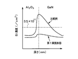
- FIG. 3 is a diagram showing the results of examining the Si concentration with respect to the substrate depth direction in the vicinity of the interface between the gate insulating film 4 and the GaN layer 2.
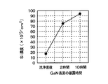
- FIG. 4 is a diagram showing the results of examining the changes in elapsed time and Si concentration when the surface of the GaN layer 2 was cleaned by performing a donor element removal step and then exposed to the atmosphere.
- a lateral HEMT that is one of GaN-HEMT (High Electron Mobility Transistor) devices is provided as a semiconductor device having a GaN device using a compound semiconductor containing GaN as a main component.
- GaN-HEMT High Electron Mobility Transistor
- the semiconductor device includes a horizontal HEMT.
- This HEMT is configured as follows.
- a horizontal HEMT is formed using a structure in which a GaN layer 2 and an n-type AlGaN layer 3 are stacked on the surface of a substrate 1 as a compound semiconductor substrate.
- Two-dimensional electron gas (hereinafter, 2DEG) carriers are induced on the GaN layer 2 side of the AlGaN / GaN interface by the GaN layer 2 and the AlGaN layer 3 due to the piezoelectric effect and the polarization effect.
- the substrate 1 is exemplified by Si (111) in FIG. 1, but is made of a semi-insulating material such as Si (111), SiC, and sapphire, or a semiconductor material.
- a GaN layer 2 and an AlGaN layer 3 are formed on the substrate 1 by, for example, heteroepitaxial growth.
- An AlGaN-GaN superlattice layer or the like may be interposed between the GaN layer 2 and the substrate 1 to improve the crystallinity of the GaN layer 2.
- the crystallinity means defects or dislocations in the GaN layer 2 and affects the electrical and optical characteristics.
- a recess-shaped part (concave part) 3 a is formed on the channel part of the compound semiconductor substrate so as to reach the GaN layer 2 from the surface of the AlGaN layer 3.
- Grooves 3b and 3c having a predetermined depth from the surface of the AlGaN layer 3 are formed on both sides of the compound semiconductor substrate with the recess-shaped part 3a interposed therebetween.
- a gate structure constituted by the gate insulating film 4 formed in the recess shape portion 3a and around the recess shape portion 3a and the gate electrode 5 formed thereon.
- the gate insulating film 4 is made of an aluminum oxide film (Al 2 O 3 ) or the like
- the gate electrode 5 is made of aluminum or poly-Si doped with impurities.
- a gate wiring layer made of Al or the like is formed on the surface of the gate electrode 5.
- materials for the gate electrode and the gate insulating film an optimum material and its structure may be selected in view of the threshold voltage, gate breakdown voltage, long-term reliability, and the like of the target device.
- the source electrode 6 is formed in the surface of the AlGaN layer 3 where the groove 3b is disposed so as to enter the groove 3b, and enters the groove 3c where the groove 3c is disposed.
- the drain electrode 7 is formed.
- the source electrode 6 and the drain electrode 7 are in ohmic contact with the surfaces of the grooves 3b and 3c, respectively.
- the horizontal HEMT according to the present embodiment is configured.
- the dimensions of each part of the horizontal HEMT configured as described above are arbitrary.
- the distance between the source-gate and the gate-drain may be determined in view of the on-resistance and breakdown voltage of the target device.
- the donor element (at the lattice position on the interface between the gate insulating film 4 and the GaN layer 2 and on the GaN layer 2 side (surface layer portion of the GaN layer 2)).
- the Si or O) concentration is set to 5.0 ⁇ 10 17 cm ⁇ 3 or less.
- the donor element concentration is set to 3.5 ⁇ 10 17 cm ⁇ 3 or less.
- the threshold voltage can be controlled to an appropriate value, and a semiconductor device having a structure capable of realizing a GaN device with little variation can be obtained.
- the horizontal HEMT configured as described above performs a switching operation by applying a gate voltage to the gate electrode 5. That is, by applying a gate voltage to the gate electrode 5, the density of the electron layer (channel) generated at the interface between the GaN layer 2 and the gate insulating film 4 below the gate electrode 5 is controlled, and between the source and drain By applying a voltage to, an operation is performed such that a current flows between the source and the drain.
- the donor element concentration is low.
- the concentration of the donor element at the interface between the gate insulating film 4 and the GaN layer 2 and the lattice position on the GaN layer 2 side is set to the low value described above. For this reason, the fluctuation
- a compound semiconductor substrate having a structure in which a GaN layer 2 and an n-type AlGaN layer 3 are laminated on the surface of a substrate 1 such as Si (111), SiC, and sapphire is prepared.
- a GaN layer 2 and an AlGaN layer 3 are formed on the surface of the substrate 1 by MOCVD (Metal Organic Chemical Vapor Deposition), ultra-high purity and high precision MBE (Molecular Beam Epitaxy). It is formed by the law.
- Step shown in FIG. 2 (b) After forming an oxide film 10 to be an interlayer film on the surface of the AlGaN layer 3, a resist 11 to be a second mask is formed on the surface of the oxide film 10. Then, after the resist 11 is patterned through a photolithography process, the oxide film 10 is patterned using the resist 11 as a mask. As a result, the resist 11 and the oxide film 10 are opened at the position where the gate structure is to be formed in the surface of the AlGaN layer 3.
- the surface of the AlGaN layer 3 is recess-processed to form a recess-shaped portion 3a in which the surface of the GaN layer 2 is exposed. Further, after forming the recess shape portion 3a, the dry etching process is completed by removing the resist 11 used as a mask for dry etching.
- Step shown in FIG. 2 (c) Subsequently, the step of forming the gate insulating film 4 is performed. After the surface of the GaN layer 2 is exposed as described above, the surface of the GaN layer 2 is exposed from the recess portion 3a before the step of forming the gate insulating film 4. A step of removing the donor element present on the surface of the GaN layer 2 is performed.
- the Si element when removing Si as a donor element, the Si element is adsorbed by performing an annealing process in an F-based gas such as CF 4 , Cl 2 -based gas, H 2 gas, or HCl gas, and a volatile gas. And then withdrawn. Thereby, Si used as a donor element can be removed.
- F-based gas such as CF 4 , Cl 2 -based gas, H 2 gas, or HCl gas
- CF 4 is introduced into the chamber at a flow rate of about 0.1 to 100 sccm, and the inside of the chamber is set to a reduced pressure atmosphere of 1 to 50 Pa. Heat to above °C.
- a mixed gas of CF 4 and H 2 or O 2 may be used.
- the chamber is heated to 500 ° C. or higher under a reduced pressure atmosphere of 0.1 to 100 Pa while introducing Cl 2 at about 5 to 100 sccm. It may also be a mixed gas containing H 2 gas and HCl gas or them.
- the adhering Si is combined with oxygen in the atmosphere and is partially in the state of SiOx, and the gas species to be used may be a gas and conditions having a property of etching Si or Si oxide.
- an active radical gas may be used using a plasma source.
- a thin film of Al or AlOx (x ⁇ 1.5) having a thickness of 5 nm or less is formed on the GaN surface, and O on the GaN surface is reacted with Al or AlOx by heating to 400 ° C. or higher. Thereafter, annealing is performed in an O 2 atmosphere to change to Al 2 O 3 . By doing so, all of the surface O can be adsorbed to Al 2 O 3 .
- the binding energy of Al—O is more stable than Ga—O, and O once taken into Al 2 O 3 does not diffuse into GaN.
- the surface Si or O when the surface Si or O is in the state of SiOx or GaOx, the surface is exposed to radical gas generated by plasma of H 2 , NF 3 (or HF) and NH 3 , and etching is removed without damage to the surface of the GaN substrate. be able to. At this time, it is also effective to heat the substrate to promote the reaction.
- the step of forming the gate insulating film 4 is performed without passing through the step of removing the donor element and the step of exposing to an atmosphere containing Si or O, or in a short time.
- the step of removing the donor element and the step of forming the gate insulating film 4 are performed in the same chamber, and these steps are integrated into a vacuum that is not exposed to the atmosphere, thereby exposing the substrate to an atmosphere containing Si or O. Can be avoided.
- the transfer from the chamber used in the donor element removal step to the chamber used in the formation process of the gate insulating film 4 may be performed by transfer in an N 2 or Ar atmosphere, or may be performed by vacuum transfer.
- An insulating film such as Al 2 O 3 , a metal material such as poly-Si doped with impurities, and a metal material such as Al are sequentially formed on the surface of the AlGaN layer 3 including the recess shape portion 3a, and then a mask (not shown) is used. These are patterned. Thereby, the gate insulating film 4 and the gate electrode 5 are formed.
- the concentration of the donor element at the lattice position on the interface between the gate insulating film 4 and the GaN layer 2 and on the GaN layer 2 side is 5. 0.0 ⁇ 10 17 cm ⁇ 3 or less, preferably 3.5 ⁇ 10 17 cm ⁇ 3 or less.
- FIG. 3 shows the results of examining the Si concentration in the substrate depth direction in the vicinity of the interface between the gate insulating film 4 and the GaN layer 2 (broken line portion in FIG. 1).
- the donor concentration decreases at the interface between the gate insulating film 4 and the GaN layer 2 and at the lattice position on the GaN layer 2 side. I know that. Specifically, it is 3.5 ⁇ 10 17 cm ⁇ 3 or less. In contrast, when the donor element removal step is not performed as a comparative example (comparative example), the donor concentration is high at the interface between the gate insulating film 4 and the GaN layer 2 and at the lattice position on the GaN layer 2 side. It was. Specifically, it exceeded 5.0 ⁇ 10 17 cm ⁇ 3 .
- FIG. 4 is a diagram showing the results of examining the changes in elapsed time and Si concentration when the surface of the GaN layer 2 was cleaned by performing a donor element removal step and then exposed to the atmosphere. As shown in this figure, as the exposure time to the atmosphere increases, the Si concentration increases. For example, 5.0 ⁇ 10 17 cm ⁇ 3 where the Si concentration can affect the threshold voltage in about 1 hour. Exceed.
- the gate insulating film 4 is formed within one hour after the donor element removal step, or Si or O
- the step of forming the gate insulating film 4 may be performed without passing through the step of exposing to an atmosphere containing oxygen. Although the O concentration is not shown, the result is the same as the Si concentration.
- the step of forming the gate insulating film 4 is performed without passing through the step of removing the donor element from the step of exposing to the atmosphere containing Si or O, or in a short time.
- the donor element concentration can be set to a low concentration as described above.
- the threshold voltage fluctuation caused by the donor in the channel portion is set by setting the donor element concentration at the interface between the gate insulating film 4 and the GaN layer 2 and the lattice position on the GaN layer 2 side in this way to a low concentration. Can be suppressed. Therefore, as compared with the conventional case where the donor element removal step is not performed, the threshold voltage can be controlled to an appropriate value, and a semiconductor having a structure capable of realizing a GaN device with less variation. It becomes possible to set it as an apparatus.
- silicon (111) When silicon (111) is used as the substrate 1, Si can be released outward from the substrate surface. For this reason, when silicon (111) is used as the substrate 1, the GaN layer 2 is formed on the substrate 1, and then a portion other than the surface of the GaN layer 2 is covered with a mask so It is preferable to suppress the release of. As a result, the donor element concentration can be further reduced, and the threshold voltage can be easily controlled to an appropriate value.
- the insulating film can be configured by forming the oxide film 12 and then forming a resist 13 serving as a mask on the surface of the oxide film 12.
- the resist 13 is removed.
- the concentration of the donor element (Si or O) at the interface between the gate insulating film 4 and the GaN layer 2 is 5.0 ⁇ 10 17 cm ⁇ 3 or more.
- the donor element concentration at the lattice position on the GaN layer 2 side (surface layer portion of the GaN layer 2) at these interfaces is 5.0 ⁇ 10 17 cm ⁇ 3 or less, preferably 3.5 ⁇ 10 17 cm ⁇ 3 or less. Is set.
- the donor element concentration at the lattice position on the GaN layer 2 side at these interfaces becomes low. By doing so, it is possible to obtain the same effect as in the first embodiment.
- a semiconductor device having a horizontal HEMT having such a structure is basically manufactured by the same manufacturing process as in the first embodiment. However, instead of the donor element removing step, a step of lowering the donor element at the lattice position in the GaN layer 2 is performed.
- a SiO 2 stable layer composed of SiO 2 that is more stable than Si in GaN is formed.
- an oxidizing atmosphere that is, an atmosphere that oxidizes GaN such as O 2 and H 2 O
- SiO 2 stable layer composed of SiO 2 that is more stable than Si in GaN.
- the bond between Si and O is stronger than the bond between Si and N
- the formation of SiO 2 prevents Si from diffusing and becoming a donor element occupying a lattice position in the GaN layer 2.
- the donor element concentration at the lattice position on the GaN layer 2 side at the interface between the gate insulating film 4 and the GaN layer 2 can be set low.
- the annealing treatment in the oxidizing atmosphere for reducing the concentration of the donor element at the lattice position on the GaN layer 2 side at the interface between the gate insulating film 4 and the GaN layer 2 is performed after the gate insulating film 4 is formed. You can go. Even if it is performed after the formation of the gate insulating film 4, since Si taken in the lattice position of the GaN layer 2 is oxidized to become SiO 2 , it is inactivated without acting as a donor element at the lattice position. The For this reason, it becomes possible to suppress the fluctuation
- the thermal budget integration of the cumulative heating temperature after the formation step of the GaN layer 2 is performed so that the donor element is not activated.
- the value may be limited to a temperature below the temperature at which the donor element is activated.
Landscapes
- Junction Field-Effect Transistors (AREA)
- Insulated Gate Type Field-Effect Transistor (AREA)
- Thin Film Transistor (AREA)
- Recrystallisation Techniques (AREA)
Abstract
半導体装置は、半絶縁性もしくは半導体にて構成される基板(1)と、前記基板上に形成されたGaN層(2)を含むチャネル形成層(2、3)と、前記チャネル形成層上に、前記GaN層に接するゲート絶縁膜(4)が形成されていると共に、該ゲート絶縁膜を介して形成されたゲート電極(5)とを有するゲート構造(4、5)と、前記チャネル形成層上において、前記ゲート構造を挟んだ両側に配置されたソース電極(6)およびドレイン電極(7)と、を備えたGaNデバイスを含む。前記ゲート絶縁膜と前記GaN層との界面および該界面より前記GaN層側における格子位置でのドナー元素濃度が5.0×1017cm-3以下に設定されている。
Description
本開示は、2014年6月26日に出願された日本出願番号2014-131692号に基づくもので、ここにその記載内容を援用する。
本開示は、窒化ガリウム(以下、GaNという)を主成分とする化合物半導体を用いたGaNデバイスを有する半導体装置およびその製造方法に関するものである。
従来より、GaNを主成分とする化合物半導体を用いたGaNデバイスを有する半導体装置が知られている。GaNデバイスを形成する場合、GaN層の表面に大気暴露によって自然酸化膜が形成されることから、ゲート絶縁膜を形成する前に自然酸化膜を除去する必要がある。しかしながら、自然酸化膜をフッ酸によって除去した場合、GaN層にダメージが残る。
このため、特許文献1において、このダメージ層を低減できるGaNデバイスの形成方法が開示されている。具体的には、GaN層にて構成される第1の半導体層の上に、第1の半導体層よりも不純物の固溶度が高い第1の犠牲層を形成する工程と、第1の犠牲層および第1の半導体層をアニールする工程とを行う。続いて、第1の犠牲層をウェットエッチングによって除去する工程を行ったのち、第1の半導体層の少なくとも一部を絶縁層で覆う工程と第1の半導体層の一部をエッチングする工程の少なくとも一方の工程を行うことで、第1の半導体層の表面のダメージを除去する。その後、第1の半導体層に電気的に接続される電極層を形成する。このようにして、GaN層の表面に形成されるダメージを除去している。
また、GaN層の表面に上部層が積層されている構造体を製造するときに、GaN層の表面が損傷しないように、その表面に形成されている自然酸化膜を除去する方法もある。具体的には、GaN層の表面を非プラズマ状態のアンモニアを含むガスに曝す工程を行い、その後、アンモニアを含むガスに暴露されたGaN層の表面を大気暴露せずにシリコン酸化(SiO2)層を積層する工程を行う。このようにして、アンモニアを含むガスを用いて自然酸化膜を除去した後、自然酸化膜が形成される前にGaN層の表面にシリコン酸化膜を除去することで、GaN層へのダメージを低減している。
しかしながら、上記したいずれの場合であっても、GaN層の表層部におけるドナー元素濃度(Si濃度もしくはO濃度)を低減することはできない。このため、GaN層の表層部に存在するSiもしくはOがドナー元素として働いてGaNデバイスの閾値電圧にバラツキが生じる。
本開示は上記点に鑑みて、閾値電圧を適正値に制御でき、バラツキの少ないGaNデバイスを実現することができる構造の半導体装置およびその製造方法を提供することを目的とする。
本開示の第一の態様において、半導体装置は、半絶縁性もしくは半導体にて構成される基板と、基板上に形成されたGaN層を含むチャネル形成層と、チャネル形成層上に、GaN層に接するゲート絶縁膜が形成されていると共に、該ゲート絶縁膜を介して形成されたゲート電極とを有するゲート構造と、チャネル形成層上において、ゲート構造を挟んだ両側に配置されたソース電極およびドレイン電極と、を備えたGaNデバイスを含む。ゲート絶縁膜とGaN層との界面および該界面よりGaN層側における格子位置でのドナー元素濃度が5.0×1017cm-3以下に設定されている。
このように、ゲート絶縁膜とGaN層との界面およびGaN層側の格子位置にあるドナー元素濃度が低い濃度に設定されているため、チャネル部のドナーに起因する閾値電圧の変動を抑制できる。したがって、閾値電圧を適正値に制御することが可能となって、バラツキの少ないGaNデバイスを実現することができる構造の半導体装置とすることが可能となる。
本開示の第二の態様において、半導体装置は、半絶縁性もしくは半導体にて構成される基板と、前記基板上に形成されたGaN層を含むチャネル形成層と、前記チャネル形成層上に、前記GaN層に接するゲート絶縁膜が形成されていると共に、該ゲート絶縁膜を介して形成されたゲート電極とを有するゲート構造と、前記チャネル形成層上において、前記ゲート構造を挟んだ両側に配置されたソース電極およびドレイン電極と、を備えたGaNデバイスを含む。ゲート絶縁膜とGaN層との界面でのドナー元素濃度が5.0×1017cm-3を超えており、ゲート絶縁膜とGaN層との界面よりGaN層側における格子位置でのドナー元素濃度が5.0×1017cm-3以下に設定されている。
このように、ゲート絶縁膜とGaN層との界面でのドナー元素濃度が5.0×1017cm-3を超えていても、ゲート絶縁膜とGaN層との界面よりGaN層側における格子位置でのドナー元素濃度が5.0×1017cm-3以下に設定されていれば、上記の第一の態様と同様の効果を得ることができる。
本開示の第三の態様において、半絶縁性もしくは半導体にて構成される基板と、前記基板上に形成されたGaN層を含むチャネル形成層と、前記チャネル形成層上に、前記GaN層に接するゲート絶縁膜が形成されていると共に、該ゲート絶縁膜を介して形成されたゲート電極とを有するゲート構造と、前記チャネル形成層上において、前記ゲート構造を挟んだ両側に配置されたソース電極およびドレイン電極と、を備えたGaNデバイスを有する半導体装置の製造方法では、基板上にGaN層を含むチャネル形成層を形成し、チャネル形成層上に、GaN層に接するゲート絶縁膜を形成し、チャネル形成層を形成し、ゲート絶縁膜を形成する前に、GaN層のうちゲート絶縁膜と接する部分に存在するドナー元素を除去し、ドナー元素を除去した後、ドナー元素を含む雰囲気に暴露することなくゲート絶縁膜を形成する。
このように、GaN層のうちゲート絶縁膜と接する部分に存在するドナー元素を除去し、ドナー元素を除去した後、ドナー元素を含む雰囲気に暴露することなくゲート絶縁膜を形成する。これにより、上記の第一の態様に記載の構造を有する半導体装置を製造できる。
本開示の第四の態様において、半絶縁性もしくは半導体にて構成される基板と、前記基板上に形成されたGaN層を含むチャネル形成層と、前記チャネル形成層上に、前記GaN層に接するゲート絶縁膜が形成されていると共に、該ゲート絶縁膜を介して形成されたゲート電極とを有するゲート構造と、前記チャネル形成層上において、前記ゲート構造を挟んだ両側に配置されたソース電極およびドレイン電極と、を備えたGaNデバイスを有する半導体装置の製造方法では、基板上にGaN層を含むチャネル形成層を形成し、チャネル形成層上に、GaN層に接するゲート絶縁膜を形成し、チャネル形成層を形成した後、ゲート絶縁膜の形成の前もしくは後に、GaN層のうちゲート絶縁膜と接する部分に存在するドナー元素を不活性化する。
このように、チャネル形成層を形成した後、ゲート絶縁膜の形成の前もしくは後に、GaN層のうちゲート絶縁膜と接する部分に存在するドナー元素を不活性化する。これにより、上記の第二の態様に記載の構造を有する半導体装置を製造できる。
本開示の第五の態様において、半絶縁性もしくは半導体にて構成される基板と、前記基板上に形成されたGaN層を含むチャネル形成層と、前記チャネル形成層上に、前記GaN層に接するゲート絶縁膜が形成されていると共に、該ゲート絶縁膜を介して形成されたゲート電極とを有するゲート構造と、前記チャネル形成層上において、前記ゲート構造を挟んだ両側に配置されたソース電極およびドレイン電極と、を備えたGaNデバイスを有する半導体装置の製造方法では、基板上にGaN層を含むチャネル形成層を形成し、チャネル形成層上に、GaN層に接するゲート絶縁膜を形成し、チャネル形成層においてGaN層を形成したのち、GaN層のうちゲート絶縁膜と接する部分に存在するドナー元素が活性化する温度以下にサーマルバジェットを制限してGaNデバイスを形成する。
このように、GaN層のうちゲート絶縁膜と接する部分に存在するドナー元素が活性化する温度以下にサーマルバジェットを制限してGaNデバイスを形成するようにしても、上記の第二の態様に記載の構造の半導体装置を製造することができる。
本開示についての上記目的およびその他の目的、特徴や利点は、添付の図面を参照しながら下記の詳細な記述により、より明確になる。その図面は、
図1は、本開示の第1実施形態にかかる半導体装置の断面図であり、
図2(a)から図2(d)は、図1に示す半導体装置の製造工程を示した断面図であり、
図3は、ゲート絶縁膜4とGaN層2の界面近傍での基板深さ方向に対するSi濃度を調べた結果を示した図であり、
図4は、ドナー元素の除去工程を行うことでGaN層2の表面洗浄を行ってから、大気へ暴露したときの経過時間とSi濃度の変化を調べた結果を示す図である。
(第1実施形態)
本開示の第1実施形態について説明する。本実施形態では、GaNを主成分とする化合物半導体を用いたGaNデバイスを有する半導体装置として、GaN-HEMT(High electron mobility transistor:高電子移動度トランジスタ)デバイスの一つである横型のHEMTを備える半導体装置について説明する。
本開示の第1実施形態について説明する。本実施形態では、GaNを主成分とする化合物半導体を用いたGaNデバイスを有する半導体装置として、GaN-HEMT(High electron mobility transistor:高電子移動度トランジスタ)デバイスの一つである横型のHEMTを備える半導体装置について説明する。
図1に示すように、本実施形態にかかる半導体装置は、横型のHEMTを備えている。このHEMTは、以下のように構成されている。
横型のHEMTは、基板1の表面に、GaN層2およびn型のAlGaN層3が積層された構造を化合物半導体基板として用いて形成されている。これらGaN層2およびAlGaN層3によるAlGaN/GaN界面のGaN層2側に、ピエゾ効果および分極効果により2次元電子ガス(以下、2DEG)キャリアが誘起される。
基板1は、図1中ではSi(111)を例として挙げているが、例えばSi(111)、SiC、およびサファイヤなどの半絶縁性材料や半導体材料によって構成されている。この基板1の上にGaN層2とAlGaN層3が例えばヘテロエピタキシャル成長によって形成されている。化合物半導体基板の比抵抗値については、目的とするデバイスの特性に応じて、化合物半導体基板を構成する各層の不純物濃度により任意に調整すれば良い。GaN層2と基板1との間にAlGaN-GaN超格子層などを介在させ、GaN層2の結晶性を良好なものにすることもできる。なお、ここでの結晶性とは、GaN層2中の欠陥や転位などであり、電気的および光学的な特性に対して影響を及ぼすものである。
この化合物半導体基板におけるチャネル部上において、AlGaN層3の表面からGaN層2に達するようにリセス形状部(凹部)3aが形成されている。また化合物半導体基板のうちリセス形状部3aを挟んだ両側において、AlGaN層3の表面から所定深さの溝部3b、3cが形成されている。
リセス形状部3aが形成された場所には、リセス形状部3a内およびリセス形状部3aの周囲に形成されたゲート絶縁膜4およびその上に形成されたゲート電極5にて構成されるゲート構造が備えられている。ゲート絶縁膜4は、酸化アルミニウム膜(Al2O3)などによって構成されており、ゲート電極5は、アルミニウムまたは不純物がドープされたPoly-Siなどによって構成されている。そして、図示しないが、ゲート電極5の表面には、Alなどで構成されるゲート配線層が形成されている。ゲート電極およびゲート絶縁膜の材料は、目的とするデバイスの閾値電圧およびゲート耐圧、長期信頼性等を鑑みて、最適な材料およびその構造を選べばよい。
一方、AlGaN層3の表面のうち溝部3bが配置された場所には、溝部3b内に入り込むようにソース電極6が形成されており、溝部3cが配置された場所には、溝部3c内に入り込むようにドレイン電極7が形成されている。そして、ソース電極6やドレイン電極7がそれぞれ溝部3b、3cの表面とオーミック接触させられている。このような構成により、本実施形態にかかる横型のHEMTが構成されている。このように構成される横型のHEMTの各部の寸法については任意であり、例えば、ソース-ゲート、ゲート-ドレイン間の距離は、目的とするデバイスのオン抵抗および耐圧を鑑みて決定すればよい。
さらに、このように構成された横型のHEMTにおいて、本実施形態では、ゲート絶縁膜4とGaN層2との界面およびGaN層2側(GaN層2の表層部)の格子位置にあるドナー元素(SiやO)濃度を5.0×1017cm-3以下に設定している。好ましくは、ドナー元素濃度を3.5×1017cm-3以下に設定している。このように、ゲート絶縁膜4とGaN層2との界面およびGaN層2側の格子位置にあるドナー元素濃度が低い濃度に設定されているため、チャネル部のドナーに起因する閾値電圧の変動を抑制できる。特に、格子位置にあるドナー元素濃度を3.5×1017cm-3以下に設定すると、より効果的に閾値電圧の変動を抑制できる。したがって、閾値電圧を適正値に制御することが可能となって、バラツキの少ないGaNデバイスを実現することができる構造の半導体装置とすることが可能となる。
具体的には、このように構成される横型のHEMTは、ゲート電極5に対してゲート電圧を印加することでスイッチング動作を行う。すなわち、ゲート電極5に対してゲート電圧を印加することで、ゲート電極5の下方におけるGaN層2とゲート絶縁膜4の界面に発生する電子層(チャネル)の密度を制御し、ソース-ドレイン間に電圧を加えることで、ソース-ドレイン間に電流を流すという動作を行う。
このような横型のHEMTでは、ゲート構造の下部におけるドナー元素濃度に応じて電子濃度などが変化し、閾値に影響を及ぼすことから、ドナー元素濃度が低い方が好ましい。これに対して、本実施形態では、ゲート絶縁膜4とGaN層2との界面およびGaN層2側の格子位置にあるドナー元素濃度を上記した低い値に設定している。このため、チャネル部のドナーに起因する閾値電圧の変動を抑制でき、閾値電圧を適正値に制御することが可能となる。これにより、バラツキの少ないGaNデバイスを実現することができる構造の半導体装置とすることが可能となる。
続いて、本実施形態にかかる横型のHEMTの製造方法について、図2を参照して説明する。
〔図2(a)に示す工程〕
Si(111)やSiCおよびサファイヤなどの基板1の表面に、GaN層2およびn型のAlGaN層3が積層された構造を有する化合物半導体基板を用意する。例えば、基板1の表面に、GaN層2およびAlGaN層3をMOCVD(Metal Organic Chemical Vapor Deposition:有機金属気相成長)法や超高純度、高精度にしたMBE(Molecular Beam Epitaxy:分子線エピタキシー)法などによって形成する。
Si(111)やSiCおよびサファイヤなどの基板1の表面に、GaN層2およびn型のAlGaN層3が積層された構造を有する化合物半導体基板を用意する。例えば、基板1の表面に、GaN層2およびAlGaN層3をMOCVD(Metal Organic Chemical Vapor Deposition:有機金属気相成長)法や超高純度、高精度にしたMBE(Molecular Beam Epitaxy:分子線エピタキシー)法などによって形成する。
〔図2(b)に示す工程〕
AlGaN層3の表面に、層間膜となる酸化膜10を形成した後、酸化膜10の表面に第2マスクとなるレジスト11を形成する。そして、フォトリソグラフィ工程を経てレジスト11をパターニングしたのち、このレジスト11をマスクとして酸化膜10をパターニングする。これにより、AlGaN層3の表面のうちゲート構造の形成予定位置においてレジスト11および酸化膜10が開口させられる。この後、レジスト11および酸化膜10をマスクとして用いたドライエッチング工程を行うことで、AlGaN層3の表面をリセス加工して、GaN層2の表面を露出させたリセス形状部3aを形成する。また、リセス形状部3aを形成した後、ドライエッチングのマスクとして用いたレジスト11を除去することで、ドライエッチング工程を終了する。
AlGaN層3の表面に、層間膜となる酸化膜10を形成した後、酸化膜10の表面に第2マスクとなるレジスト11を形成する。そして、フォトリソグラフィ工程を経てレジスト11をパターニングしたのち、このレジスト11をマスクとして酸化膜10をパターニングする。これにより、AlGaN層3の表面のうちゲート構造の形成予定位置においてレジスト11および酸化膜10が開口させられる。この後、レジスト11および酸化膜10をマスクとして用いたドライエッチング工程を行うことで、AlGaN層3の表面をリセス加工して、GaN層2の表面を露出させたリセス形状部3aを形成する。また、リセス形状部3aを形成した後、ドライエッチングのマスクとして用いたレジスト11を除去することで、ドライエッチング工程を終了する。
〔図2(c)に示す工程〕
続いて、ゲート絶縁膜4の形成工程を行うが、上記のようにしてGaN層2の表面を露出させたのち、ゲート絶縁膜4の形成工程の前に、リセス形状部3aから露出させられたGaN層2の表面に存在するドナー元素の除去工程を行う。
続いて、ゲート絶縁膜4の形成工程を行うが、上記のようにしてGaN層2の表面を露出させたのち、ゲート絶縁膜4の形成工程の前に、リセス形状部3aから露出させられたGaN層2の表面に存在するドナー元素の除去工程を行う。
例えば、ドナー元素としてSiを除去する場合には、CF4などのF系ガス、Cl2系ガス、H2ガス、HClガス中においてアニール処理を行うことにより、Si元素が吸着され、揮発性ガスとなって離脱していく。これにより、ドナー元素となるSiを除去することができる。
例えば、CHF3、SF6やCF4などのF系ガスを用いる場合、CF4を0.1~100sccm程度の流量でチャンバー内に導入しつつ、チャンバー内を1~50Paの減圧雰囲気とし、500℃以上に加熱する。このとき、CF4とH2やO2の混合ガスを用いてもよい。Cl2系ガスを用いる場合、Cl2を5~100sccm程度導入しつつ、チャンバー内を0.1~100Paの減圧雰囲気とし、500℃以上に加熱する。また、H2ガスやHClガスやそれらを含む混合ガスを用いてもよい。付着するSiは大気中の酸素と結合し、部分的にSiOxの状態になっており、用いるガス種は、SiやSi酸化物をエッチングする性質のガス及び条件を用いればよい。また、加熱だけではSi、SiOxの除去が困難な場合には、プラズマ源を用いて活性なラジカルガスを用いても良い。
また、ドナー元素としてOを除去する場合には、Alによる酸素捕捉効果を用いてO元素を還元するのも有効である。例えば、5nm以下の薄膜のAl若しくはAlOx(x<1.5)をGaN表面に成膜し、400℃以上に加熱することでGaN表面のOをAlもしくはAlOxと反応させる。その後にO2雰囲気でアニールすることでAl2O3に変質させる。こうすることで表面のOをすべてAl2O3に吸着できる。Al-Oの結合エネルギーはGa-Oよりも安定であり一度Al2O3に取り込まれたOがGaN中に拡散することはない。
また、表面のSiやOがSiOxやGaOxの状態である場合には、H2、NF3(もしくはHF)およびNH3のプラズマによるラジカルガスに晒すことでGaN基板表面へのダメージなくエッチング除去することができる。この際に反応促進のために基板を加熱することも有効である。
この後、ドナー元素の除去工程からSiやOを含有する雰囲気中への暴露工程を経ることなく、もしくは短時間しか経ないようにして、ゲート絶縁膜4の形成工程を行う。例えば、ドナー元素の除去工程とゲート絶縁膜4の形成工程を同じチャンバーで行いつつ、これらの工程を大気に曝さない真空一貫工程とすることにより、SiやOを含有する雰囲気中への暴露工程を経ないようにできる。また、ドナー元素の除去工程で用いるチャンバーからゲート絶縁膜4の形成工程で用いるチャンバーへの搬送をN2やAr雰囲気での搬送によって行えるようにしたり、真空搬送によって行えるようにしても良い。
そして、リセス形状部3a内を含め、AlGaN層3の表面にAl2O3などの絶縁膜、不純物をドープしたPoly-Si、Alなどの金属材料を順に成膜したのち、図示しないマスクを用いてこれらをパターニングする。これにより、ゲート絶縁膜4、ゲート電極5が形成される。
このとき、ドナー元素の除去工程を行ってからゲート絶縁膜4を形成しているため、ゲート絶縁膜4とGaN層2との界面およびGaN層2側の格子位置にあるドナー元素の濃度が5.0×1017cm-3以下、好ましくは3.5×1017cm-3以下となる。図3は、ゲート絶縁膜4とGaN層2の界面近傍(図1中の破線部分)での基板深さ方向に対するSi濃度を調べた結果を示している。この図に示すように、本実施形態のようなドナー元素の除去工程を行った場合、ゲート絶縁膜中4とGaN層2との界面およびGaN層2側の格子位置においてドナー濃度が小さくなっていることが判る。具体的には、3.5×1017cm-3以下となっている。これに対して、比較例としてドナー元素の除去工程を行わなかった場合(比較例)、ゲート絶縁膜中4とGaN層2との界面およびGaN層2側の格子位置においてドナー濃度が高くなっていた。具体的には、5.0×1017cm-3を超えていた。
これは、ドナー元素の除去工程を行った後、SiやOなどを含む雰囲気、例えば大気への暴露工程を行うことなくゲート絶縁膜4を形成したためである。図4は、ドナー元素の除去工程を行うことでGaN層2の表面洗浄を行ってから、大気へ暴露したときの経過時間とSi濃度の変化を調べた結果を示す図である。この図に示すように、大気への暴露時間の増加に伴ってSi濃度が高くなっていき、例えば1時間程度でSi濃度が閾値電圧に影響を与え得る5.0×1017cm-3を超える。このため、Si濃度を5.0×1017cm-3以下とするためには、ドナー元素の除去工程を行ってから、1時間以内にゲート絶縁膜4の形成工程を行うか、SiやOを含む雰囲気への暴露工程を経ないようにしてゲート絶縁膜4の形成工程を行うようにすればよい。なお、O濃度については図示していないが、Si濃度と同様の結果となる。
したがって、本実施形態のように、ドナー元素の除去工程からSiやOを含有する雰囲気中への暴露工程を経ることなく、もしくは短時間しか経ないようにして、ゲート絶縁膜4の形成工程を行うことで、ドナー元素濃度を上記のように低い濃度に設定できる。
そして、このようにゲート絶縁膜4とGaN層2との界面およびGaN層2側の格子位置にあるドナー元素濃度が低い濃度に設定されることで、チャネル部のドナーに起因する閾値電圧の変動を抑制することが可能となる。したがって、従来のように、ドナー元素の除去工程を行わない場合と比較して、閾値電圧を適正値に制御することが可能となって、バラツキの少ないGaNデバイスを実現することができる構造の半導体装置とすることが可能となる。
なお、基板1としてシリコン(111)を用いる場合には、基板表面からのSiの外方への放出も発生し得る。このため、基板1としてシリコン(111)を用いる場合には、基板1の上にGaN層2を成膜したのち、GaN層2の表面以外の部分をマスクによって覆うことで、Siの外方への放出を抑制すると好ましい。これにより、よりドナー元素濃度を低く抑えることが可能となり、さらに閾値電圧を適正値に制御することが容易となる。
〔図2(d)に示す工程〕
ゲート絶縁膜4、ゲート電極5を覆いつつ、溝部3b、3cの形成予定領域が開口する絶縁膜およびマスクを形成する。例えば、絶縁膜については酸化膜12を形成した後、酸化膜12の表面にマスクとなるレジスト13を形成することで構成することができる。
ゲート絶縁膜4、ゲート電極5を覆いつつ、溝部3b、3cの形成予定領域が開口する絶縁膜およびマスクを形成する。例えば、絶縁膜については酸化膜12を形成した後、酸化膜12の表面にマスクとなるレジスト13を形成することで構成することができる。
この後、レジスト13を用いて酸化膜12およびAlGaN層3のドライエッチング工程を行うことで、AlGaN層3の表面に溝部3b、3cを形成する。この後、レジスト13を除去する。
この後の工程については従来と同様であるが、層間絶縁膜形成工程やコンタクトホール形成工程、ソース電極6およびドレイン電極7の形成工程などを経て、図1に示した横型のHEMTを有する半導体装置が完成する。
(第2実施形態)
本開示の第2実施形態について説明する。本実施形態は、第1実施形態に対して化合物半導体基板中におけるドナー元素濃度が異なっているが、その他に関しては第1実施形態と同様であるため、第1実施形態と異なる部分についてのみ説明する。
本開示の第2実施形態について説明する。本実施形態は、第1実施形態に対して化合物半導体基板中におけるドナー元素濃度が異なっているが、その他に関しては第1実施形態と同様であるため、第1実施形態と異なる部分についてのみ説明する。
本実施形態にかかる横型のHEMTを有する半導体装置では、ゲート絶縁膜4とGaN層2との界面にあるドナー元素(SiやO)濃度が5.0×1017cm-3以上となっている。ただし、これらの界面におけるGaN層2側(GaN層2の表層部)の格子位置にあるドナー元素濃度を5.0×1017cm-3以下、好ましくは3.5×1017cm-3以下に設定している。このように、ゲート絶縁膜4とGaN層2との界面にあるドナー元素濃度が高い濃度に設定されていたとしても、これらの界面におけるGaN層2側の格子位置にあるドナー元素濃度が低くなるようにすれば、第1実施形態と同様の効果を得ることが可能となる。
このような構造の横型のHEMTを有する半導体装置は、基本的には第1実施形態と同様の製造工程によって製造される。ただし、ドナー元素の除去工程に代えて、GaN層2中の格子位置のドナー元素を低くする工程を行うようにしている。
例えば、酸化雰囲気、つまりO2やH2OなどのようにGaNを酸化する雰囲気でのアニール処理を行うことにより、GaN中のSiよりも安定なSiO2で構成されるSiO2安定層を形成する。SiとOとの結合の方がSiとNとの結合よりも強いため、SiO2を形成しておくことにより、Siが拡散してGaN層2中の格子位置を占めるドナー元素とならないように不活性化できる。これにより、ゲート絶縁膜4とGaN層2との界面におけるGaN層2側の格子位置にあるドナー元素濃度を低く設定することが可能となる。
なお、このようにゲート絶縁膜4とGaN層2との界面におけるGaN層2側の格子位置にあるドナー元素濃度を低くするための酸化雰囲気でのアニール処理は、ゲート絶縁膜4の成膜後に行っても構わない。ゲート絶縁膜4の成膜後に行ったとしても、GaN層2の格子位置に取り込まれたSiが酸化されることでSiO2になるため、格子位置にあるドナー元素として働かずに不活性化される。このため、閾値電圧の変動を抑制することが可能になる。また、このような酸化雰囲気でのアニール処理を行った場合には、後工程で他のアニール処理を行うときに、酸化雰囲気でのアニール処理によって形成したSi安定層が乖離しない温度およびサーマルバジェット以下で行う必要がある。
(他の実施形態)
例えば、上記第2実施形態では、ドナー元素を不活性化する工程を行う場合について説明したが、ドナー元素が活性化しないように、GaN層2の形成工程以降のサーマルバジェット(累積加熱温度の積分値)をドナー元素を活性化させる温度以下に制限しても良い。
例えば、上記第2実施形態では、ドナー元素を不活性化する工程を行う場合について説明したが、ドナー元素が活性化しないように、GaN層2の形成工程以降のサーマルバジェット(累積加熱温度の積分値)をドナー元素を活性化させる温度以下に制限しても良い。
本開示は、実施例に準拠して記述されたが、本開示は当該実施例や構造に限定されるものではないと理解される。本開示は、様々な変形例や均等範囲内の変形をも包含する。加えて、様々な組み合わせや形態、さらには、それらに一要素のみ、それ以上、あるいはそれ以下、を含む他の組み合わせや形態をも、本開示の範疇や思想範囲に入るものである。
Claims (10)
- 半絶縁性もしくは半導体にて構成される基板(1)と、
前記基板上に形成されたGaN層(2)を含むチャネル形成層(2、3)と、
前記チャネル形成層上に、前記GaN層に接するゲート絶縁膜(4)が形成されていると共に、該ゲート絶縁膜を介して形成されたゲート電極(5)とを有するゲート構造(4、5)と、
前記チャネル形成層上において、前記ゲート構造を挟んだ両側に配置されたソース電極(6)およびドレイン電極(7)と、を備えたGaNデバイスを含み、
前記ゲート絶縁膜と前記GaN層との界面および該界面より前記GaN層側における格子位置でのドナー元素濃度が5.0×1017cm-3以下に設定されている半導体装置。 - 半絶縁性もしくは半導体にて構成される基板(1)と、
前記基板上に形成されたGaN層(2)を含むチャネル形成層(2、3)と、
前記チャネル形成層上に、前記GaN層に接するゲート絶縁膜(4)が形成されていると共に、該ゲート絶縁膜を介して形成されたゲート電極(5)とを有するゲート構造(4、5)と、
前記チャネル形成層上において、前記ゲート構造を挟んだ両側に配置されたソース電極(6)およびドレイン電極(7)と、を備えたGaNデバイスを含み、
前記ゲート絶縁膜と前記GaN層との界面でのドナー元素濃度が5.0×1017cm-3を超えており、前記ゲート絶縁膜と前記GaN層との界面より前記GaN層側における格子位置でのドナー元素濃度が5.0×1017cm-3以下に設定されている半導体装置。 - 前記ドナー元素はSiもしくはOである請求項1または2に記載の半導体装置。
- 前記ドナー元素は、前記格子位置において3.5×1017cm-3以下に設定されている請求項1ないし3のいずれか1つに記載の半導体装置。
- 半絶縁性もしくは半導体にて構成される基板(1)と、
前記基板上に形成されたGaN層(2)を含むチャネル形成層(2、3)と、
前記チャネル形成層上に、前記GaN層に接するゲート絶縁膜(4)が形成されていると共に、該ゲート絶縁膜を介して形成されたゲート電極(5)とを有するゲート構造(4、5)と、
前記チャネル形成層上において、前記ゲート構造を挟んだ両側に配置されたソース電極(6)およびドレイン電極(7)と、を備えたGaNデバイスを有する半導体装置の製造方法であって、
前記基板上に前記GaN層を含むチャネル形成層を形成し、
前記チャネル形成層上に、前記GaN層に接するゲート絶縁膜を形成し、
前記チャネル形成層を形成した後、前記ゲート絶縁膜を形成する前に、前記GaN層のうち前記ゲート絶縁膜と接する部分に存在するドナー元素を除去することを備え、
前記ドナー元素の除去の後、前記ドナー元素を含む雰囲気に暴露することなく前記ゲート絶縁膜の形成を行う半導体装置の製造方法。 - 前記チャネル形成層の上に前記ゲート構造の形成予定位置が開口するマスク(10、11)を形成し、該マスクを用いたエッチングにより前記GaN層を露出させるリセス形状部(3a)を形成することをさらに備え、
前記リセス形状部を形成した後に、前記ドナー元素の除去を行う請求項5に記載の半導体装置の製造方法。 - 前記ドナー元素の除去は、F系ガス、Cl2系ガス、H2ガス、HClガスのいずれかを用いたアニール処理である請求項5または6に記載の半導体装置の製造方法。
- 半絶縁性もしくは半導体にて構成される基板(1)と、
前記基板上に形成されたGaN層(2)を含むチャネル形成層(2、3)と、
前記チャネル形成層上に、前記GaN層に接するゲート絶縁膜(4)が形成されていると共に、該ゲート絶縁膜を介して形成されたゲート電極(5)とを有するゲート構造(4、5)と、
前記チャネル形成層上において、前記ゲート構造を挟んだ両側に配置されたソース電極(6)およびドレイン電極(7)と、を備えたGaNデバイスを有する半導体装置の製造方法であって、
前記基板上に前記GaN層を含むチャネル形成層を形成し、
前記チャネル形成層上に、前記GaN層に接するゲート絶縁膜を形成し、
前記チャネル形成層の形成の後、前記ゲート絶縁膜の形成の前もしくは後に、前記GaN層のうち前記ゲート絶縁膜と接する部分に存在するドナー元素を不活性化することを備える半導体装置の製造方法。 - 前記ドナー元素の不活性化は、酸化雰囲気中でのアニール処理である請求項8に記載の半導体装置の製造方法。
- 半絶縁性もしくは半導体にて構成される基板(1)と、
前記基板上に形成されたGaN層(2)を含むチャネル形成層(2、3)と、
前記チャネル形成層上に、前記GaN層に接するゲート絶縁膜(4)が形成されていると共に、該ゲート絶縁膜を介して形成されたゲート電極(5)とを有するゲート構造(4、5)と、
前記チャネル形成層上において、前記ゲート構造を挟んだ両側に配置されたソース電極(6)およびドレイン電極(7)と、を備えたGaNデバイスを有する半導体装置の製造方法であって、
前記基板上に前記GaN層を含むチャネル形成層を形成し、
前記チャネル形成層上に、前記GaN層に接するゲート絶縁膜を形成し、
前記チャネル形成層において前記GaN層を形成したのち、前記GaN層のうち前記ゲート絶縁膜と接する部分に存在するドナー元素が活性化する温度以下にサーマルバジェットを制限して前記GaNデバイスを形成することを備える半導体装置の製造方法。
Priority Applications (1)
| Application Number | Priority Date | Filing Date | Title |
|---|---|---|---|
| US15/320,799 US10121663B2 (en) | 2014-06-26 | 2015-03-26 | Semiconductor device and method for producing same |
Applications Claiming Priority (2)
| Application Number | Priority Date | Filing Date | Title |
|---|---|---|---|
| JP2014131692A JP6308049B2 (ja) | 2014-06-26 | 2014-06-26 | 半導体装置の製造方法 |
| JP2014-131692 | 2014-06-26 |
Publications (1)
| Publication Number | Publication Date |
|---|---|
| WO2015198512A1 true WO2015198512A1 (ja) | 2015-12-30 |
Family
ID=54937626
Family Applications (1)
| Application Number | Title | Priority Date | Filing Date |
|---|---|---|---|
| PCT/JP2015/001761 Ceased WO2015198512A1 (ja) | 2014-06-26 | 2015-03-26 | 半導体装置およびその製造方法 |
Country Status (3)
| Country | Link |
|---|---|
| US (1) | US10121663B2 (ja) |
| JP (1) | JP6308049B2 (ja) |
| WO (1) | WO2015198512A1 (ja) |
Cited By (1)
| Publication number | Priority date | Publication date | Assignee | Title |
|---|---|---|---|---|
| CN108735811A (zh) * | 2017-04-24 | 2018-11-02 | 株式会社东芝 | 半导体装置、电源电路以及计算机 |
Families Citing this family (2)
| Publication number | Priority date | Publication date | Assignee | Title |
|---|---|---|---|---|
| WO2019009111A1 (ja) * | 2017-07-07 | 2019-01-10 | パナソニックIpマネジメント株式会社 | 半導体装置およびその製造方法 |
| US11916119B2 (en) * | 2021-11-03 | 2024-02-27 | Globalfoundries U.S. Inc. | Transistor with self-aligned gate and self-aligned source/drain terminal(s) and methods |
Citations (4)
| Publication number | Priority date | Publication date | Assignee | Title |
|---|---|---|---|---|
| WO2009113612A1 (ja) * | 2008-03-12 | 2009-09-17 | 日本電気株式会社 | 半導体装置 |
| JP2010010584A (ja) * | 2008-06-30 | 2010-01-14 | Sharp Corp | ヘテロ接合電界効果トランジスタおよびヘテロ接合電界効果トランジスタの製造方法 |
| JP2012231003A (ja) * | 2011-04-26 | 2012-11-22 | Advanced Power Device Research Association | 半導体装置 |
| JP2014078568A (ja) * | 2012-10-09 | 2014-05-01 | Sumitomo Electric Ind Ltd | 半導体装置 |
Family Cites Families (13)
| Publication number | Priority date | Publication date | Assignee | Title |
|---|---|---|---|---|
| JP3169066B2 (ja) * | 1997-10-17 | 2001-05-21 | 日本電気株式会社 | 電界効果トランジスタおよびその製造方法 |
| JP2002110962A (ja) * | 2000-09-27 | 2002-04-12 | Toshiba Corp | 半導体装置及びその製造方法 |
| US6773504B2 (en) * | 2001-04-12 | 2004-08-10 | Sumitomo Electric Industries, Ltd. | Oxygen doping method to gallium nitride single crystal substrate and oxygen-doped N-type gallium nitride freestanding single crystal substrate |
| US7091524B2 (en) * | 2003-03-25 | 2006-08-15 | Matsushita Electric Industrial Co., Ltd. | Semiconductor device and method for fabricating the same |
| JP4575745B2 (ja) | 2004-10-18 | 2010-11-04 | 株式会社豊田中央研究所 | GaN系半導体層に上部層が積層されている半導体装置の製造方法 |
| US7932539B2 (en) * | 2005-11-29 | 2011-04-26 | The Hong Kong University Of Science And Technology | Enhancement-mode III-N devices, circuits, and methods |
| JP2007335677A (ja) * | 2006-06-15 | 2007-12-27 | Furukawa Electric Co Ltd:The | Iii族窒化物半導体を用いたノーマリオフ型電界効果トランジスタ及びその製造方法 |
| JP5510325B2 (ja) * | 2008-08-06 | 2014-06-04 | 日本電気株式会社 | 電界効果トランジスタ |
| JP2010098076A (ja) | 2008-10-15 | 2010-04-30 | Sumitomo Electric Device Innovations Inc | 半導体装置の製造方法 |
| JP5506055B2 (ja) | 2011-01-25 | 2014-05-28 | 古河電気工業株式会社 | 半導体装置の製造方法 |
| JP5902010B2 (ja) | 2012-03-19 | 2016-04-13 | トランスフォーム・ジャパン株式会社 | 化合物半導体装置及びその製造方法 |
| US9000484B2 (en) * | 2012-05-23 | 2015-04-07 | Hrl Laboratories, Llc | Non-uniform lateral profile of two-dimensional electron gas charge density in type III nitride HEMT devices using ion implantation through gray scale mask |
| US9570600B2 (en) * | 2012-11-16 | 2017-02-14 | Massachusetts Institute Of Technology | Semiconductor structure and recess formation etch technique |
-
2014
- 2014-06-26 JP JP2014131692A patent/JP6308049B2/ja not_active Expired - Fee Related
-
2015
- 2015-03-26 WO PCT/JP2015/001761 patent/WO2015198512A1/ja not_active Ceased
- 2015-03-26 US US15/320,799 patent/US10121663B2/en not_active Expired - Fee Related
Patent Citations (4)
| Publication number | Priority date | Publication date | Assignee | Title |
|---|---|---|---|---|
| WO2009113612A1 (ja) * | 2008-03-12 | 2009-09-17 | 日本電気株式会社 | 半導体装置 |
| JP2010010584A (ja) * | 2008-06-30 | 2010-01-14 | Sharp Corp | ヘテロ接合電界効果トランジスタおよびヘテロ接合電界効果トランジスタの製造方法 |
| JP2012231003A (ja) * | 2011-04-26 | 2012-11-22 | Advanced Power Device Research Association | 半導体装置 |
| JP2014078568A (ja) * | 2012-10-09 | 2014-05-01 | Sumitomo Electric Ind Ltd | 半導体装置 |
Cited By (2)
| Publication number | Priority date | Publication date | Assignee | Title |
|---|---|---|---|---|
| CN108735811A (zh) * | 2017-04-24 | 2018-11-02 | 株式会社东芝 | 半导体装置、电源电路以及计算机 |
| CN108735811B (zh) * | 2017-04-24 | 2021-02-12 | 株式会社东芝 | 半导体装置、电源电路以及计算机 |
Also Published As
| Publication number | Publication date |
|---|---|
| US20170162391A1 (en) | 2017-06-08 |
| US10121663B2 (en) | 2018-11-06 |
| JP6308049B2 (ja) | 2018-04-11 |
| JP2016009843A (ja) | 2016-01-18 |
Similar Documents
| Publication | Publication Date | Title |
|---|---|---|
| JP6337726B2 (ja) | 半導体装置およびその製造方法 | |
| TWI723777B (zh) | 半導體元件之製造方法及電漿處理裝置 | |
| CN107946358B (zh) | 一种与Si-CMOS工艺兼容的AlGaN/GaN异质结HEMT器件及其制作方法 | |
| JP5653607B2 (ja) | GaN系電界効果トランジスタおよびその製造方法 | |
| JP5345328B2 (ja) | 半導体装置の製造方法 | |
| JP5566670B2 (ja) | GaN系電界効果トランジスタ | |
| JP2010192633A (ja) | GaN系電界効果トランジスタの製造方法 | |
| JP2009010107A (ja) | 半導体装置及びその製造方法 | |
| JP6287143B2 (ja) | 半導体装置およびその製造方法 | |
| CN108198855B (zh) | 半导体元件、半导体基底及其形成方法 | |
| WO2013005667A1 (ja) | GaN系半導体素子の製造方法 | |
| CN103930978A (zh) | 场效应晶体管及其制造方法 | |
| US20160013305A1 (en) | Nitride semiconductor device and method for manufacturing nitride semiconductor device | |
| JP5920255B2 (ja) | 半導体装置の製造方法およびそれに用いられるドライエッチング装置 | |
| KR20190112523A (ko) | 이종접합 전계효과 트랜지스터 및 그 제조 방법 | |
| JP6308049B2 (ja) | 半導体装置の製造方法 | |
| CN103597582B (zh) | 氮化物半导体装置及其制造方法 | |
| JP2007150106A (ja) | Iii族窒化物半導体基板 | |
| CN112216741A (zh) | 高电子迁移率晶体管的绝缘结构以及其制作方法 | |
| JP5463529B2 (ja) | 電界効果トランジスタの製造方法 | |
| CN113140630A (zh) | 增强型HEMT的p型氮化物栅的制备方法及应用其制备增强型氮化物HEMT的方法 | |
| JP6447231B2 (ja) | 半導体装置およびその製造方法 | |
| JP2010165783A (ja) | 電界効果型トランジスタおよびその製造方法 | |
| JP7388545B2 (ja) | 半導体装置の製造方法 | |
| JP2007200975A (ja) | 半導体装置とその製造法 |
Legal Events
| Date | Code | Title | Description |
|---|---|---|---|
| 121 | Ep: the epo has been informed by wipo that ep was designated in this application |
Ref document number: 15811040 Country of ref document: EP Kind code of ref document: A1 |
|
| WWE | Wipo information: entry into national phase |
Ref document number: 15320799 Country of ref document: US |
|
| NENP | Non-entry into the national phase |
Ref country code: DE |
|
| 122 | Ep: pct application non-entry in european phase |
Ref document number: 15811040 Country of ref document: EP Kind code of ref document: A1 |