WO2015198510A1 - 半導体基板の欠陥領域の評価方法 - Google Patents
半導体基板の欠陥領域の評価方法 Download PDFInfo
- Publication number
- WO2015198510A1 WO2015198510A1 PCT/JP2015/001431 JP2015001431W WO2015198510A1 WO 2015198510 A1 WO2015198510 A1 WO 2015198510A1 JP 2015001431 W JP2015001431 W JP 2015001431W WO 2015198510 A1 WO2015198510 A1 WO 2015198510A1
- Authority
- WO
- WIPO (PCT)
- Prior art keywords
- semiconductor substrate
- region
- defect
- evaluated
- flat band
- Prior art date
- Legal status (The legal status is an assumption and is not a legal conclusion. Google has not performed a legal analysis and makes no representation as to the accuracy of the status listed.)
- Ceased
Links
Images




Classifications
-
- G—PHYSICS
- G01—MEASURING; TESTING
- G01R—MEASURING ELECTRIC VARIABLES; MEASURING MAGNETIC VARIABLES
- G01R31/00—Arrangements for testing electric properties; Arrangements for locating electric faults; Arrangements for electrical testing characterised by what is being tested not provided for elsewhere
- G01R31/26—Testing of individual semiconductor devices
- G01R31/2607—Circuits therefor
- G01R31/2637—Circuits therefor for testing other individual devices
- G01R31/2639—Circuits therefor for testing other individual devices for testing field-effect devices, e.g. of MOS-capacitors
-
- C—CHEMISTRY; METALLURGY
- C30—CRYSTAL GROWTH
- C30B—SINGLE-CRYSTAL GROWTH; UNIDIRECTIONAL SOLIDIFICATION OF EUTECTIC MATERIAL OR UNIDIRECTIONAL DEMIXING OF EUTECTOID MATERIAL; REFINING BY ZONE-MELTING OF MATERIAL; PRODUCTION OF A HOMOGENEOUS POLYCRYSTALLINE MATERIAL WITH DEFINED STRUCTURE; SINGLE CRYSTALS OR HOMOGENEOUS POLYCRYSTALLINE MATERIAL WITH DEFINED STRUCTURE; AFTER-TREATMENT OF SINGLE CRYSTALS OR A HOMOGENEOUS POLYCRYSTALLINE MATERIAL WITH DEFINED STRUCTURE; APPARATUS THEREFOR
- C30B29/00—Single crystals or homogeneous polycrystalline material with defined structure characterised by the material or by their shape
- C30B29/02—Elements
- C30B29/06—Silicon
-
- C—CHEMISTRY; METALLURGY
- C30—CRYSTAL GROWTH
- C30B—SINGLE-CRYSTAL GROWTH; UNIDIRECTIONAL SOLIDIFICATION OF EUTECTIC MATERIAL OR UNIDIRECTIONAL DEMIXING OF EUTECTOID MATERIAL; REFINING BY ZONE-MELTING OF MATERIAL; PRODUCTION OF A HOMOGENEOUS POLYCRYSTALLINE MATERIAL WITH DEFINED STRUCTURE; SINGLE CRYSTALS OR HOMOGENEOUS POLYCRYSTALLINE MATERIAL WITH DEFINED STRUCTURE; AFTER-TREATMENT OF SINGLE CRYSTALS OR A HOMOGENEOUS POLYCRYSTALLINE MATERIAL WITH DEFINED STRUCTURE; APPARATUS THEREFOR
- C30B33/00—After-treatment of single crystals or homogeneous polycrystalline material with defined structure
-
- C—CHEMISTRY; METALLURGY
- C30—CRYSTAL GROWTH
- C30B—SINGLE-CRYSTAL GROWTH; UNIDIRECTIONAL SOLIDIFICATION OF EUTECTIC MATERIAL OR UNIDIRECTIONAL DEMIXING OF EUTECTOID MATERIAL; REFINING BY ZONE-MELTING OF MATERIAL; PRODUCTION OF A HOMOGENEOUS POLYCRYSTALLINE MATERIAL WITH DEFINED STRUCTURE; SINGLE CRYSTALS OR HOMOGENEOUS POLYCRYSTALLINE MATERIAL WITH DEFINED STRUCTURE; AFTER-TREATMENT OF SINGLE CRYSTALS OR A HOMOGENEOUS POLYCRYSTALLINE MATERIAL WITH DEFINED STRUCTURE; APPARATUS THEREFOR
- C30B33/00—After-treatment of single crystals or homogeneous polycrystalline material with defined structure
- C30B33/005—Oxydation
-
- C—CHEMISTRY; METALLURGY
- C30—CRYSTAL GROWTH
- C30B—SINGLE-CRYSTAL GROWTH; UNIDIRECTIONAL SOLIDIFICATION OF EUTECTIC MATERIAL OR UNIDIRECTIONAL DEMIXING OF EUTECTOID MATERIAL; REFINING BY ZONE-MELTING OF MATERIAL; PRODUCTION OF A HOMOGENEOUS POLYCRYSTALLINE MATERIAL WITH DEFINED STRUCTURE; SINGLE CRYSTALS OR HOMOGENEOUS POLYCRYSTALLINE MATERIAL WITH DEFINED STRUCTURE; AFTER-TREATMENT OF SINGLE CRYSTALS OR A HOMOGENEOUS POLYCRYSTALLINE MATERIAL WITH DEFINED STRUCTURE; APPARATUS THEREFOR
- C30B33/00—After-treatment of single crystals or homogeneous polycrystalline material with defined structure
- C30B33/02—Heat treatment
-
- H—ELECTRICITY
- H10—SEMICONDUCTOR DEVICES; ELECTRIC SOLID-STATE DEVICES NOT OTHERWISE PROVIDED FOR
- H10P—GENERIC PROCESSES OR APPARATUS FOR THE MANUFACTURE OR TREATMENT OF DEVICES COVERED BY CLASS H10
- H10P74/00—Testing or measuring during manufacture or treatment of wafers, substrates or devices
- H10P74/20—Testing or measuring during manufacture or treatment of wafers, substrates or devices characterised by the properties tested or measured, e.g. structural or electrical properties
- H10P74/207—Electrical properties, e.g. testing or measuring of resistance, deep levels or capacitance-voltage characteristics
-
- H—ELECTRICITY
- H10—SEMICONDUCTOR DEVICES; ELECTRIC SOLID-STATE DEVICES NOT OTHERWISE PROVIDED FOR
- H10P—GENERIC PROCESSES OR APPARATUS FOR THE MANUFACTURE OR TREATMENT OF DEVICES COVERED BY CLASS H10
- H10P74/00—Testing or measuring during manufacture or treatment of wafers, substrates or devices
- H10P74/23—Testing or measuring during manufacture or treatment of wafers, substrates or devices characterised by multiple measurements, corrections, marking or sorting processes
-
- H—ELECTRICITY
- H10—SEMICONDUCTOR DEVICES; ELECTRIC SOLID-STATE DEVICES NOT OTHERWISE PROVIDED FOR
- H10P—GENERIC PROCESSES OR APPARATUS FOR THE MANUFACTURE OR TREATMENT OF DEVICES COVERED BY CLASS H10
- H10P74/00—Testing or measuring during manufacture or treatment of wafers, substrates or devices
- H10P74/23—Testing or measuring during manufacture or treatment of wafers, substrates or devices characterised by multiple measurements, corrections, marking or sorting processes
- H10P74/235—Testing or measuring during manufacture or treatment of wafers, substrates or devices characterised by multiple measurements, corrections, marking or sorting processes comprising optical enhancement of defects or not-directly-visible states
-
- C—CHEMISTRY; METALLURGY
- C30—CRYSTAL GROWTH
- C30B—SINGLE-CRYSTAL GROWTH; UNIDIRECTIONAL SOLIDIFICATION OF EUTECTIC MATERIAL OR UNIDIRECTIONAL DEMIXING OF EUTECTOID MATERIAL; REFINING BY ZONE-MELTING OF MATERIAL; PRODUCTION OF A HOMOGENEOUS POLYCRYSTALLINE MATERIAL WITH DEFINED STRUCTURE; SINGLE CRYSTALS OR HOMOGENEOUS POLYCRYSTALLINE MATERIAL WITH DEFINED STRUCTURE; AFTER-TREATMENT OF SINGLE CRYSTALS OR A HOMOGENEOUS POLYCRYSTALLINE MATERIAL WITH DEFINED STRUCTURE; APPARATUS THEREFOR
- C30B15/00—Single-crystal growth by pulling from a melt, e.g. Czochralski method
- C30B15/20—Controlling or regulating
-
- C—CHEMISTRY; METALLURGY
- C30—CRYSTAL GROWTH
- C30B—SINGLE-CRYSTAL GROWTH; UNIDIRECTIONAL SOLIDIFICATION OF EUTECTIC MATERIAL OR UNIDIRECTIONAL DEMIXING OF EUTECTOID MATERIAL; REFINING BY ZONE-MELTING OF MATERIAL; PRODUCTION OF A HOMOGENEOUS POLYCRYSTALLINE MATERIAL WITH DEFINED STRUCTURE; SINGLE CRYSTALS OR HOMOGENEOUS POLYCRYSTALLINE MATERIAL WITH DEFINED STRUCTURE; AFTER-TREATMENT OF SINGLE CRYSTALS OR A HOMOGENEOUS POLYCRYSTALLINE MATERIAL WITH DEFINED STRUCTURE; APPARATUS THEREFOR
- C30B15/00—Single-crystal growth by pulling from a melt, e.g. Czochralski method
- C30B15/30—Mechanisms for rotating or moving either the melt or the crystal
-
- H—ELECTRICITY
- H10—SEMICONDUCTOR DEVICES; ELECTRIC SOLID-STATE DEVICES NOT OTHERWISE PROVIDED FOR
- H10P—GENERIC PROCESSES OR APPARATUS FOR THE MANUFACTURE OR TREATMENT OF DEVICES COVERED BY CLASS H10
- H10P74/00—Testing or measuring during manufacture or treatment of wafers, substrates or devices
- H10P74/20—Testing or measuring during manufacture or treatment of wafers, substrates or devices characterised by the properties tested or measured, e.g. structural or electrical properties
- H10P74/203—Structural properties, e.g. testing or measuring thicknesses, line widths, warpage, bond strengths or physical defects
Definitions
- the present invention relates to a method for evaluating a defect region of a semiconductor substrate.
- a semiconductor silicon wafer (hereinafter referred to as a wafer) is used as a substrate for an integrated circuit.
- a region for forming an element of an integrated circuit is a region having no defect.
- defects included in a wafer for example, there is a grown-in defect taken in when a semiconductor single crystal is manufactured by a CZ method or the like.
- defects include those having no atoms at the regular crystal lattice positions (vacancies) and those having atoms between the lattice positions (interstitial silicon).
- a region containing a lot of vacancies is called a V region, and a region containing a lot of interstitial silicon is called an I region.
- the concentration of vacancies and interstitial silicon is determined from the relationship between the crystal pulling rate (growth rate) in the CZ method and the temperature gradient near the solid-liquid interface in the crystal.
- growth rate crystal pulling rate
- the N region there is a region where a defect called an oxidation-induced stacking fault (OSF) occurs. It is considered that an N region where no OSF is generated is desirable for making an element of an integrated circuit.
- OSF oxidation-induced stacking fault
- Patent Documents 1-3 have a problem in that it is necessary to perform heat treatment a plurality of times or to complicate the treatment such as forcibly contaminating the surface.
- the conventional evaluation method evaluates the presence or absence of oxygen precipitation and the post-contamination gettering ability, so that a Ni region (N region, a region where interstitial defects are dominant) or Nv region (N region).
- Ni region N region, a region where interstitial defects are dominant
- Nv region N region
- the present invention has been made in view of the above problems, and provides a method for evaluating a defect region of a semiconductor substrate that can determine the defect region of a semiconductor substrate by a simple method even at a low oxygen concentration. For the purpose.
- the present invention relates to a method for evaluating a defect region of a semiconductor substrate, wherein the defect region of a semiconductor substrate is evaluated from the CV characteristics of a MOS structure formed on the semiconductor substrate.
- the defect region and the flat band voltage or fixed charge density are the same under the same heat treatment conditions and CV characteristic evaluation conditions as those for evaluating the defect region of the semiconductor substrate to be evaluated.
- the defect area obtained in advance from the flat band voltage or the fixed charge density obtained from the CV characteristics of the MOS structure formed on the semiconductor substrate is obtained.
- the determination of the defect region of the semiconductor substrate to be evaluated is based on the N region and the N region where the defect region is the V region and the N region where the vacancy defect is dominant but the vacancy defect is dominant. However, it can be determined which of the Ni region where the interstitial defects are dominant and the I region where the interstitial defects are dominant. Such determination can be suitably performed as the determination of the defect region of the semiconductor substrate to be evaluated.
- a defective region of a semiconductor substrate can be determined with high accuracy by a simple method even if the semiconductor substrate has a low oxygen concentration.
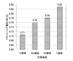
- FIG. 5 is an enlarged view of a rising portion of the CV characteristic in FIG. 2. It is a figure which shows the flat band voltage ( Vfb ) of the semiconductor substrate which has various defect areas. It is a figure which shows the fixed charge density ( Qd ) of the semiconductor substrate which has various defect areas. It is a figure which shows the relationship between a fixed charge density and a defect area
- the present inventor has intensively studied a method for evaluating a defect region of a semiconductor substrate that can determine the defect region of the semiconductor substrate by a simple method even at a low oxygen concentration.
- the inventor firstly explained that the amount of change in the flat band voltage (Vfb) in the CV characteristic of a MOS (Metal-Oxide-Silicon) capacitor is the fixed charge density in the oxide film when the impurity concentration of the semiconductor substrate is the same.
- Vfb flat band voltage
- MOS Metal-Oxide-Silicon
- V fb the flat band voltage
- the flat band voltage (V fb ) is an externally applied voltage necessary to eliminate the above-mentioned energy band bending and make it flat.
- the flat band voltage (V fb ) is when the work function of the metal electrode is W m , the Fermi level of the semiconductor substrate is E f , the thickness of the oxide film is dox, and the fixed charge amount in the oxide film is Q s ( 1) It is given by the formula.
- V fb (W m ⁇ E f ) + (Q s / dox) (1)
- the work function W m of the metal electrode is a value determined by the material of the metal electrode, and the Fermi level E f of the semiconductor substrate is expressed by the equation (2).
- E i ⁇ E f (kT / q) ⁇ log (N sub / n i ) (2)
- E f is the Fermi level
- E i is the intrinsic Fermi level
- k is the Boltzmann coefficient
- T is the temperature
- q is the elementary charge
- Nsub is the impurity concentration of the semiconductor substrate
- ni is the intrinsic carrier concentration.
- the capacitance C of the MOS capacitor in the flat band state is a series junction of the oxide film capacitance Cox and the depletion layer capacitance Cd, and is expressed by equation (3).
- C Cox ⁇ C d / (C ox + C d ) (3)
- oxide film capacitance Cox ⁇ o ⁇ S / dox (4)
- C d ⁇ ⁇ S / Ld (5)
- L d (kT ⁇ ⁇ / N sub ⁇ q 2 ) 1/2 (6)
- S is the area of the capacitor
- ⁇ o and ⁇ are the dielectric constant of the oxide film and the dielectric constant of the semiconductor substrate, respectively.
- the fixed charge in the oxide film is generally a positive charge, and a part of interstitial silicon generated when a silicon single crystal is thermally oxidized to form an oxide film as shown in the following chemical formula (8). Is thought to be left behind in the oxide film. Si + O 2 ⁇ SiO 2 + (Si + ) (8)
- the most common method for forming an oxide film is a high-temperature heat treatment in an oxygen atmosphere or a water vapor atmosphere. In this method, silicon in the substrate is consumed to form an oxide film.
- the present inventor found that the fixed charge in the oxide film is derived from interstitial silicon, and when the oxide film is formed by consuming silicon of the substrate such as thermal oxidation, the fixed charge in the oxide film is We thought that there was a correlation between the amount of interstitial silicon and vacancies contained in the substrate. Furthermore, since the present inventor can calculate the fixed charge density by using the flat band voltage of the CV characteristic as described above, the silicon single crystal can be calculated from the flat band voltage value of the CV characteristic or the fixed charge density value. The amount of interstitial silicon and vacancies in the semiconductor substrate can be estimated, and the defect region of the semiconductor substrate is determined from the flat band voltage or fixed charge density obtained from the CV characteristics of the MOS structure formed in the semiconductor substrate. Thus, even when the semiconductor substrate has a low oxygen concentration, it has been found that the defect region of the semiconductor substrate can be determined with high accuracy by a simple method, and the present invention has been made.
- the C-V characteristic of is measured (see step S11 in FIG. 1).
- the defect region type of the semiconductor substrate whose C-V characteristics are measured in step S11 is, for example, the defect region type of the single crystal silicon ingot from which the semiconductor substrate is cut out using the evaluation method disclosed in Patent Document 1.
- the density of the precipitate can be calculated and determined in advance based on the density of the oxygen precipitate.
- the MOS structure can be manufactured, for example, by forming a thermal oxide film on a semiconductor substrate and forming a metal electrode having a predetermined area on the thermal oxide film.
- the mercury probe is used. When is used, the formation of the metal electrode can be omitted.
- a flat band voltage or a fixed charge density is obtained from the CV characteristic measured in step S11 (see step S12 in FIG. 1). Specifically, since the flat band voltage V fb and the impurity concentration N sub of the semiconductor substrate can be calculated from the result of the CV characteristic, if the CV characteristic can be obtained, the flat band voltage V fb is calculated. If the flat band voltage V fb is known, the fixed charge amount Q s can be calculated from the equations (1) and (2), and the fixed charge density Q d expressed by the equation (7) can be calculated. Can also be calculated.
- the relationship between the defect region and the flat band voltage or fixed charge density is obtained (see step S13 in FIG. 1). Specifically, based on the flat band voltage V fb or the fixed charge density Q d obtained in step S12, the type of the defect region is associated with the value range of the flat band voltage V fb or the fixed charge density Q d .
- the types of defect regions for example, V region where vacancy defects are dominant, Nv region where N defects are dominant but vacancy defects are dominant, and N region, but there are interstitial defects. Ni region which is dominant and I region where interstitial defects are dominant.
- the MOS structure of the semiconductor substrate to be evaluated can also be produced, for example, by forming a thermal oxide film on the semiconductor substrate and forming a metal electrode having a predetermined area on the thermal oxide film. When a mercury probe is used in the measurement, the formation of the metal electrode can be omitted.
- a flat band voltage or a fixed charge density is obtained from the CV characteristics measured in step S14 (see step S15 in FIG. 1). Specifically, the flat band voltage V fb or the fixed charge density Q d is calculated from the CV characteristic in the same manner as in step S12.
- the defect region of the evaluation target semiconductor substrate is determined. Determination is made (see step S16 in FIG. 1).
- the determination of the defect region of the semiconductor substrate to be evaluated is the V region or N region in which the vacancy defects are dominant, but the Nv region or N region in which the vacancy defects are dominant. It can be determined which of the Ni region where the interstitial defects are dominant and the I region where the interstitial defects are dominant. Such determination can be suitably performed as the determination of the defect region of the semiconductor substrate to be evaluated.
- the defect region of the semiconductor substrate is determined with high accuracy by a simple method. be able to.
- a p-type silicon single crystal ingot having a diameter of 300 mm, an axial orientation of ⁇ 100>, a resistivity of 10 to 30 ⁇ ⁇ cm, and an oxygen concentration of 15 ppma (JEIDA) was produced using the CZ method.
- the vacancy defects are dominant (V region)
- the N region is the vacancy defect dominant (Nv Region)
- N region is the vacancy defect dominant (Nv Region)
- I region interstitial defect dominant
- the density of oxygen precipitates was calculated using the evaluation method disclosed in Patent Document 1, and the determination was made based on the density of oxygen precipitates.
- these wafers were cleaned by RCA cleaning, and heat-treated in a vertical heat treatment furnace at 900 ° C. in an oxygen atmosphere to form a 25 nm thermal oxide film on the front and back surfaces of the wafer. Thereafter, the oxide film on the back surface of the wafers was removed using HF vapor.
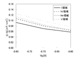
- FIG. 2 shows a CV characteristic curve of a wafer in which the defect regions are the V region, the Nv region, the Ni region, and the I region, respectively.
- the horizontal axis represents the bias voltage Vg, and the vertical axis represents the capacitance C / S normalized by the capacitor area. It can be seen that the shape of the CV characteristic curve in any defect area is almost the same, but the rising position is deviated.
- FIG. 3 shows an enlarged view of the rising portion of the CV characteristic curve shown in FIG.
- the rising positions are more clearly shifted in different defect areas, and the CV characteristic curve shifts to the negative side in the defect areas with more interstitial silicon and fewer vacancies. Recognize.
- the density of oxygen precipitates is calculated using the evaluation method disclosed in Patent Document 1 for wafers having the same crystal as each of the evaluation target wafers 1 to 5, and the defect region is determined based on the calculated density of oxygen precipitates. Determined the type. The results are shown in Table 1.
- the determination result according to the present invention coincides with the result determined from the density of oxygen precipitates using the evaluation method shown in Patent Document 1. Therefore, it can be seen that the defect region can be determined with high accuracy by the evaluation method using the fixed charge density of the present invention. Further, in this method, since the fixed charge density in the oxide film is calculated and the determination is performed based on the calculated fixed charge density, the defect region is determined regardless of the oxygen concentration of the semiconductor substrate to be evaluated. It is possible.
- the present invention is not limited to the above embodiment.
- the above-described embodiment is an exemplification, and the present invention has substantially the same configuration as the technical idea described in the claims of the present invention, and any device that exhibits the same function and effect is the present invention. It is included in the technical scope of the invention.
Landscapes
- Chemical & Material Sciences (AREA)
- Engineering & Computer Science (AREA)
- Crystallography & Structural Chemistry (AREA)
- Materials Engineering (AREA)
- Metallurgy (AREA)
- Organic Chemistry (AREA)
- Physics & Mathematics (AREA)
- Thermal Sciences (AREA)
- Power Engineering (AREA)
- General Physics & Mathematics (AREA)
- Testing Or Measuring Of Semiconductors Or The Like (AREA)
- Crystals, And After-Treatments Of Crystals (AREA)
Abstract
Description
例えば、特許文献1や特許文献2で示された方法のように、ウェーハ片に熱処理を行い、ウェーハ内部の酸素析出物密度を測定し、その値より結晶欠陥領域を判別する方法がある。
また、従来の評価方法は、酸素析出の有無や、汚染後ゲッタリング能力を評価することで、Ni領域(N領域であるが、格子間欠陥が優勢な領域)やNv領域(N領域であるが、空孔欠陥が優勢な領域)を判定しているが、ウェーハ中の酸素濃度が低くなると酸素が析出しにくくなるので、欠陥領域の判定が困難になるという問題があった。
評価対象半導体基板の欠陥領域の判定として、このような判定を好適に行うことができる。
前述のように、半導体単結晶を製造する際には、結晶欠陥領域を制御することが重要になっており、そのためにもGrown-in欠陥を検出・評価する技術が必要となってきている。Grown-in欠陥を検出・評価する方法は多く報告されており、特許文献1-3に示された方法があるが、これらの方法は、複数回熱処理を実施する必要があったり、表面を強制汚染させたり、と複雑な処理が必要になるという問題があった。
また、従来の評価方法は、酸素析出の有無や、汚染後ゲッタリング能力を評価することで、Ni領域やNv領域を判定しているが、ウェーハ中の酸素濃度が低くなると酸素が析出しにくくなるので、欠陥領域の判定が困難になるという問題があった。
本発明者は、まず、MOS(Metal-Oxide-Silicon)キャパシタのC-V特性中のフラットバンド電圧(Vfb)の変化量は、半導体基板の不純物濃度が同じ場合、酸化膜中の固定電荷密度によって決まることと、酸化膜中の固定電荷は酸化膜中の格子間シリコンに由来するという点に着目した。
まず、理想状態ではMOS構造のエネルギーバンド図は外部からの印加電圧が無い場合、バンドに曲がりはなく平ら(フラット)であり、外部から電圧が印加されてバンドが曲がる。
ここで、理想状態とは、電極の仕事関数と半導体基板のフェルミ準位に差がなく、酸化膜中に固定電荷が存在していない状態である。
しかしながら、理想的な状態と異なり、一般的なMOSキャパシタでは、金属電極の仕事関数と半導体基板のフェルミ準位に差があり、また、酸化膜中に固定電荷が存在するため、外部から電圧が印加されていない状態でもエネルギーバンドは曲がっている。
フラットバンド電圧(Vfb)は、金属電極の仕事関数をWm、半導体基板のフェルミ準位をEf、酸化膜の厚さをdox、酸化膜中の固定電荷量をQsとしたとき(1)式で与えられる。
Vfb=(Wm-Ef)+(Qs/dox) ・・・(1)
Ei-Ef=(kT/q)・log(Nsub/ni) ・・・(2)
(2)式から、温度が一定の条件の下では、フェルミ準位Efは半導体基板の不純物濃度Nsubによってその値が決まることがわかる。
C=Cox・Cd/(Cox+Cd) ・・・(3)
Cox=εo・S/dox ・・・(4)
Cd=ε・S/Ld ・・・(5)
Ld=(kT・ε/Nsub・q2)1/2 ・・・(6)
ここで、Sはキャパシタの面積、εo、εはそれぞれ酸化膜の誘電率、半導体基板の誘電率である。
Qd=Qs/(S・q) ・・・(7)
酸化膜中の固定電荷は一般的に正の電荷であり、以下に示す化学式(8)のように、シリコン単結晶を熱酸化して酸化膜を形成するときに発生する格子間シリコンの一部が酸化膜中に取り残されたものと考えられている。
Si+O2→SiO2+(Si+) ・・・(8)
さらに、本発明者は上述のように固定電荷密度はC-V特性のフラットバンド電圧を用いることで算出できるため、C-V特性のフラットバンド電圧の値又は固定電荷密度の値よりシリコン単結晶中の格子間シリコンや空孔の量を推定できると考え、半導体基板に形成されたMOS構造のC-V特性から求められるフラットバンド電圧又は固定電荷密度から、半導体基板の欠陥領域を判定することで、半導体基板が低酸素濃度であっても簡便な方法で半導体基板の欠陥領域を高精度で判定することができることを見出し、本発明をなすに至った。
まず、欠陥領域のタイプが分かっている半導体基板を用いて、評価対象半導体基板の欠陥領域を評価するときと同じ熱処理条件、及び、CーV特性評価条件で、半導体基板に形成されたMOS構造のCーV特性を測定する(図1のステップS11参照)。
なお、ステップS11でCーV特性を測定する半導体基板の欠陥領域のタイプは、例えば、半導体基板が切り出される単結晶シリコンインゴットの欠陥領域のタイプを特許文献1に示される評価方法を用いて酸素析出物の密度を算出し、酸素析出物の密度に基づいて
予め判定しておくことができる。
また、MOS構造は、例えば、半導体基板上に熱酸化膜を形成し、熱酸化膜上に所定の面積の金属電極を形成することで作製することができ、C-V特性の測定において水銀プローバを用いる場合には、金属電極の形成を省略することができる。
具体的には、フラットバンド電圧Vfbや半導体基板の不純物濃度NsubはC-V特性の結果より算出することができるので、C-V特性を求めることができれば、フラットバンド電圧Vfbを算出することができ、フラットバンド電圧Vfbがわかれば、(1)式、(2)式から固定電荷量Qsを算出することができ、さらに(7)式で表される固定電荷密度Qdも算出することができる。
具体的には、ステップS12で求めたフラットバンド電圧Vfb又は固定電荷密度Qdに基づいて、欠陥領域のタイプと、フラットバンド電圧Vfb又は固定電荷密度Qdの値の範囲とを関連づける。
ここで、欠陥領域のタイプとしては、例えば、空孔欠陥が優勢なものであるV領域、N領域であるが空孔欠陥が優勢なものであるNv領域、N領域であるが格子間欠陥が優勢なものであるNi領域、格子間欠陥が優勢なものであるI領域が挙げられる。
評価対象半導体基板のMOS構造についても、例えば、半導体基板上に熱酸化膜を形成し、熱酸化膜上に所定の面積の金属電極を形成することで作製することができ、C-V特性の測定において水銀プローバを用いる場合には、金属電極の形成を省略することができる。
具体的には、ステップS12と同様にして、CーV特性からフラットバンド電圧Vfb又は固定電荷密度Qdを算出する。
なお、評価対象半導体基板の欠陥領域の判定は、欠陥領域が、空孔欠陥が優勢なものであるV領域、N領域であるが空孔欠陥が優勢なものであるNv領域、N領域であるが格子間欠陥が優勢なものであるNi領域、格子間欠陥が優勢なものであるI領域のうちのいずれであるかを判定するものとすることができる。
評価対象半導体基板の欠陥領域の判定として、このような判定を好適に行うことができる。
まず、直径300mmで、軸方位が<100>であり、抵抗率が10~30Ω・cmで、酸素濃度が15ppma(JEIDA)であるp型のシリコン単結晶インゴットをCZ法を用いて作製した。
CZ法による作製時には、引き上げ速度を変化させ、結晶内の欠陥の濃度を変化させることで、空孔欠陥が優勢なもの(V領域)、N領域であるが空孔欠陥が優勢なもの(Nv領域)、N領域であるが格子間欠陥が優勢なもの(Ni領域)、格子間欠陥が優勢なもの(I領域)をそれぞれ作製し、その単結晶インゴットを用いて、スライス工程、研磨工程によりポリッシュドウェーハ(半導体基板)を作製した。
欠陥領域がそれぞれV領域、Nv領域、Ni領域、I領域であるウェーハのC-V特性カーブを図2に示す。横軸はバイアス電圧Vg、縦軸はキャパシタ面積で規格化した容量C/Sをそれぞれ表している。いずれの欠陥領域でのC-V特性カーブの形状はほぼ同じであるが、立ち上がりの位置がずれていることがわかる。
なお、フラットバンド電圧Vfbと欠陥領域のタイプとの関係についても、図6と同様に定義することができる。
なお、フラットバンド電圧Vfbと欠陥領域のタイプとの関係が定義されていれば、フラットバンド電圧Vfbから欠陥領域のタイプを同様に決定することができる。

従って、本発明の固定電荷密度を用いる評価方法により、欠陥領域の判定を高精度で行うことが可能となることがわかる。
また、この方法は、酸化膜中の固定電荷密度を算出し、算出された固定電荷密度に基づいて判定を行っているため、評価対象半導体基板の酸素濃度によらずに欠陥領域の判定を行うことが可能である。
Claims (2)
- 半導体基板の欠陥領域を半導体基板に形成されたMOS構造のC-V特性から評価する半導体基板の欠陥領域の評価方法であって、
予め、欠陥領域のタイプがわかっている半導体基板を用いて、評価対象半導体基板の欠陥領域を評価するときと同じ熱処理条件、及び、C-V特性評価条件で、欠陥領域とフラットバンド電圧又は固定電荷密度との関係を求めておき、
評価対象半導体基板の欠陥領域の評価では、半導体基板に形成されたMOS構造のC-V特性から求められたフラットバンド電圧又は固定電荷密度から、予め求められている欠陥領域とフラットバンド電圧又は固定電荷密度との関係に基づき、評価対象半導体基板の欠陥領域を判定することを特徴とする半導体基板の欠陥領域の評価方法。 - 評価対象半導体基板の欠陥領域の前記判定は、欠陥領域が、空孔欠陥が優勢なものであるV領域、N領域であるが空孔欠陥が優勢なものであるNv領域、N領域であるが格子間欠陥が優勢なものであるNi領域、格子間欠陥が優勢なものであるI領域のうちのいずれであるかを判定するものであることを特徴とする請求項1に記載の半導体基板の欠陥領域の評価方法。
Priority Applications (4)
| Application Number | Priority Date | Filing Date | Title |
|---|---|---|---|
| US15/309,584 US9958493B2 (en) | 2014-06-25 | 2015-03-16 | Method for evaluating defect region of semiconductor substrate |
| CN201580030897.5A CN106663643B (zh) | 2014-06-25 | 2015-03-16 | 半导体基板的缺陷区域的评价方法 |
| DE112015002612.6T DE112015002612B4 (de) | 2014-06-25 | 2015-03-16 | Verfahren zum Bewerten einer Defektregion eines Halbleitersubstrats |
| KR1020167033541A KR102185648B1 (ko) | 2014-06-25 | 2015-03-16 | 반도체 기판의 결함영역의 평가방법 |
Applications Claiming Priority (2)
| Application Number | Priority Date | Filing Date | Title |
|---|---|---|---|
| JP2014-129850 | 2014-06-25 | ||
| JP2014129850A JP6119680B2 (ja) | 2014-06-25 | 2014-06-25 | 半導体基板の欠陥領域の評価方法 |
Publications (1)
| Publication Number | Publication Date |
|---|---|
| WO2015198510A1 true WO2015198510A1 (ja) | 2015-12-30 |
Family
ID=54937624
Family Applications (1)
| Application Number | Title | Priority Date | Filing Date |
|---|---|---|---|
| PCT/JP2015/001431 Ceased WO2015198510A1 (ja) | 2014-06-25 | 2015-03-16 | 半導体基板の欠陥領域の評価方法 |
Country Status (6)
| Country | Link |
|---|---|
| US (1) | US9958493B2 (ja) |
| JP (1) | JP6119680B2 (ja) |
| KR (1) | KR102185648B1 (ja) |
| CN (1) | CN106663643B (ja) |
| DE (1) | DE112015002612B4 (ja) |
| WO (1) | WO2015198510A1 (ja) |
Families Citing this family (5)
| Publication number | Priority date | Publication date | Assignee | Title |
|---|---|---|---|---|
| CN109946577B (zh) * | 2019-01-31 | 2020-08-21 | 西安电子科技大学 | 一种GaN器件电应力可靠性的测试方法 |
| JP7588495B2 (ja) * | 2020-11-06 | 2024-11-22 | 一般財団法人電力中央研究所 | 半導体ウエーハの評価装置、及び、半導体ウエーハの製造方法 |
| CN113138195A (zh) * | 2021-04-16 | 2021-07-20 | 上海新昇半导体科技有限公司 | 晶体缺陷的监控方法及晶棒生长方法 |
| KR102871902B1 (ko) | 2023-12-04 | 2025-10-17 | 주식회사 코탁스 | Ai 학습을 이용한, pcb 보드 상의 칩 새틀링 영상 모니터링 시스템 |
| JP2025112209A (ja) * | 2024-01-18 | 2025-07-31 | 信越半導体株式会社 | シリコン単結晶基板の欠陥領域の判定方法 |
Citations (2)
| Publication number | Priority date | Publication date | Assignee | Title |
|---|---|---|---|---|
| JPH06302665A (ja) * | 1993-04-14 | 1994-10-28 | Hitachi Ltd | 欠陥位置解析方法 |
| JP2005045216A (ja) * | 2003-06-13 | 2005-02-17 | Solid State Measurements Inc | フレキシブルメンブレインプローブおよびその使用方法 |
Family Cites Families (13)
| Publication number | Priority date | Publication date | Assignee | Title |
|---|---|---|---|---|
| JP2874834B2 (ja) * | 1994-07-29 | 1999-03-24 | 三菱マテリアル株式会社 | シリコンウェーハのイントリンシックゲッタリング処理法 |
| JPH08102481A (ja) * | 1994-09-30 | 1996-04-16 | Shin Etsu Handotai Co Ltd | Mis型半導体装置の評価方法 |
| US5714679A (en) * | 1996-10-02 | 1998-02-03 | Nichols; Steven J. | Portable apparatus for testing an internal combustion engine |
| JP3787472B2 (ja) | 1999-11-12 | 2006-06-21 | 信越半導体株式会社 | シリコンウエーハおよびその製造方法ならびにシリコンウエーハの評価方法 |
| US20110263126A1 (en) * | 2000-11-22 | 2011-10-27 | Sumco Corporation | Method for manufacturing a silicon wafer |
| JP3994665B2 (ja) | 2000-12-28 | 2007-10-24 | 信越半導体株式会社 | シリコン単結晶ウエーハおよびシリコン単結晶の製造方法 |
| US7029933B2 (en) * | 2004-06-22 | 2006-04-18 | Tech Semiconductor Singapore Pte. Ltd. | Method for monitoring ion implant doses |
| CN1727872A (zh) * | 2004-07-29 | 2006-02-01 | 上海华虹Nec电子有限公司 | 一种离子束应用于金属硅化物工艺缺陷分析的方法 |
| US7846822B2 (en) * | 2004-07-30 | 2010-12-07 | The Board Of Trustees Of The University Of Illinois | Methods for controlling dopant concentration and activation in semiconductor structures |
| JP2006278892A (ja) | 2005-03-30 | 2006-10-12 | Toshiba Ceramics Co Ltd | シリコン単結晶ウェーハの品質評価方法 |
| JP4316533B2 (ja) | 2005-04-27 | 2009-08-19 | 株式会社東芝 | 半導体装置の評価方法 |
| JP4894351B2 (ja) | 2006-05-18 | 2012-03-14 | 信越半導体株式会社 | 半導体基板の評価方法 |
| US8803533B2 (en) * | 2011-01-06 | 2014-08-12 | University Of South Florida | Noncontact determination of interface trap density for semiconductor-dielectric interface structures |
-
2014
- 2014-06-25 JP JP2014129850A patent/JP6119680B2/ja active Active
-
2015
- 2015-03-16 US US15/309,584 patent/US9958493B2/en active Active
- 2015-03-16 DE DE112015002612.6T patent/DE112015002612B4/de active Active
- 2015-03-16 CN CN201580030897.5A patent/CN106663643B/zh active Active
- 2015-03-16 KR KR1020167033541A patent/KR102185648B1/ko active Active
- 2015-03-16 WO PCT/JP2015/001431 patent/WO2015198510A1/ja not_active Ceased
Patent Citations (2)
| Publication number | Priority date | Publication date | Assignee | Title |
|---|---|---|---|---|
| JPH06302665A (ja) * | 1993-04-14 | 1994-10-28 | Hitachi Ltd | 欠陥位置解析方法 |
| JP2005045216A (ja) * | 2003-06-13 | 2005-02-17 | Solid State Measurements Inc | フレキシブルメンブレインプローブおよびその使用方法 |
Also Published As
| Publication number | Publication date |
|---|---|
| JP2016009772A (ja) | 2016-01-18 |
| KR102185648B1 (ko) | 2020-12-02 |
| US20170160335A1 (en) | 2017-06-08 |
| DE112015002612B4 (de) | 2023-04-27 |
| JP6119680B2 (ja) | 2017-04-26 |
| DE112015002612T5 (de) | 2017-03-16 |
| CN106663643A (zh) | 2017-05-10 |
| KR20170018309A (ko) | 2017-02-17 |
| CN106663643B (zh) | 2019-05-17 |
| US9958493B2 (en) | 2018-05-01 |
Similar Documents
| Publication | Publication Date | Title |
|---|---|---|
| JP6119680B2 (ja) | 半導体基板の欠陥領域の評価方法 | |
| JPWO2001055485A1 (ja) | シリコンウエーハおよびシリコン単結晶の製造条件を決定する方法ならびにシリコンウエーハの製造方法 | |
| CN107251210A (zh) | 半导体基板的评价方法及半导体基板的制造方法 | |
| CN101606239A (zh) | 硅晶片的评价方法 | |
| US9500694B2 (en) | Method for evaluating wafer defects | |
| JP2019137566A (ja) | シリコン結晶中の炭素濃度測定方法 | |
| JPH1050715A (ja) | シリコンウェーハとその製造方法 | |
| JP5434491B2 (ja) | 半導体基板の評価方法及び半導体デバイスの製造方法 | |
| JP6268676B2 (ja) | 電極の形成方法 | |
| JP5590002B2 (ja) | 金属汚染評価方法及びエピタキシャルウェーハの製造方法 | |
| KR102661941B1 (ko) | 웨이퍼의 결함 영역의 평가 방법 | |
| JP5561245B2 (ja) | 半導体基板の評価方法 | |
| JP5742742B2 (ja) | 金属汚染評価方法 | |
| CN109075076B (zh) | 硅晶片 | |
| JP6003447B2 (ja) | 半導体基板の金属汚染評価方法および半導体基板の製造方法 | |
| JP5720557B2 (ja) | 半導体基板の評価方法および半導体基板の製造方法 | |
| JP6713493B2 (ja) | エピタキシャルシリコンウェーハの製造方法及びエピタキシャルシリコンウェーハ | |
| JP4200845B2 (ja) | シリコン単結晶インゴットの点欠陥分布を測定する方法 | |
| JP2019050322A (ja) | シリコン中の炭素測定方法 | |
| JP5949303B2 (ja) | エピタキシャル成長炉の評価方法およびエピタキシャルウェーハの製造方法 | |
| JP6031971B2 (ja) | 半導体試料の電気的評価方法および評価装置 | |
| JP5742739B2 (ja) | 金属汚染評価用シリコン基板の選別方法 | |
| JP5211750B2 (ja) | 単結晶シリコンウエーハの製造方法 | |
| CN111051580A (zh) | 硅晶片 | |
| JP2017183471A (ja) | 点欠陥領域の評価方法 |
Legal Events
| Date | Code | Title | Description |
|---|---|---|---|
| 121 | Ep: the epo has been informed by wipo that ep was designated in this application |
Ref document number: 15811546 Country of ref document: EP Kind code of ref document: A1 |
|
| WWE | Wipo information: entry into national phase |
Ref document number: 15309584 Country of ref document: US |
|
| ENP | Entry into the national phase |
Ref document number: 20167033541 Country of ref document: KR Kind code of ref document: A |
|
| WWE | Wipo information: entry into national phase |
Ref document number: 112015002612 Country of ref document: DE |
|
| 122 | Ep: pct application non-entry in european phase |
Ref document number: 15811546 Country of ref document: EP Kind code of ref document: A1 |