WO2015190610A1 - 回路基板及び回路基板におけるノイズ低減方法 - Google Patents
回路基板及び回路基板におけるノイズ低減方法 Download PDFInfo
- Publication number
- WO2015190610A1 WO2015190610A1 PCT/JP2015/067090 JP2015067090W WO2015190610A1 WO 2015190610 A1 WO2015190610 A1 WO 2015190610A1 JP 2015067090 W JP2015067090 W JP 2015067090W WO 2015190610 A1 WO2015190610 A1 WO 2015190610A1
- Authority
- WO
- WIPO (PCT)
- Prior art keywords
- electromagnetic
- band gap
- circuit board
- pattern
- gap structure
- Prior art date
- Legal status (The legal status is an assumption and is not a legal conclusion. Google has not performed a legal analysis and makes no representation as to the accuracy of the status listed.)
- Ceased
Links
Images


Classifications
-
- H—ELECTRICITY
- H05—ELECTRIC TECHNIQUES NOT OTHERWISE PROVIDED FOR
- H05K—PRINTED CIRCUITS; CASINGS OR CONSTRUCTIONAL DETAILS OF ELECTRIC APPARATUS; MANUFACTURE OF ASSEMBLAGES OF ELECTRICAL COMPONENTS
- H05K1/00—Printed circuits
- H05K1/02—Details
- H05K1/0213—Electrical arrangements not otherwise provided for
- H05K1/0216—Reduction of cross-talk, noise or electromagnetic interference
- H05K1/0236—Electromagnetic band-gap structures
-
- H—ELECTRICITY
- H05—ELECTRIC TECHNIQUES NOT OTHERWISE PROVIDED FOR
- H05K—PRINTED CIRCUITS; CASINGS OR CONSTRUCTIONAL DETAILS OF ELECTRIC APPARATUS; MANUFACTURE OF ASSEMBLAGES OF ELECTRICAL COMPONENTS
- H05K1/00—Printed circuits
- H05K1/02—Details
- H05K1/0213—Electrical arrangements not otherwise provided for
- H05K1/0237—High frequency adaptations
- H05K1/025—Impedance arrangements, e.g. impedance matching, reduction of parasitic impedance
-
- H—ELECTRICITY
- H05—ELECTRIC TECHNIQUES NOT OTHERWISE PROVIDED FOR
- H05K—PRINTED CIRCUITS; CASINGS OR CONSTRUCTIONAL DETAILS OF ELECTRIC APPARATUS; MANUFACTURE OF ASSEMBLAGES OF ELECTRICAL COMPONENTS
- H05K1/00—Printed circuits
- H05K1/02—Details
- H05K1/0296—Conductive pattern lay-out details not covered by sub groups H05K1/02 - H05K1/0295
- H05K1/0298—Multilayer circuits
-
- H—ELECTRICITY
- H05—ELECTRIC TECHNIQUES NOT OTHERWISE PROVIDED FOR
- H05K—PRINTED CIRCUITS; CASINGS OR CONSTRUCTIONAL DETAILS OF ELECTRIC APPARATUS; MANUFACTURE OF ASSEMBLAGES OF ELECTRICAL COMPONENTS
- H05K1/00—Printed circuits
- H05K1/16—Printed circuits incorporating printed electric components, e.g. printed resistors, capacitors or inductors
Definitions
- the present invention relates to a circuit board on which electronic components are mounted and a noise reduction method in the circuit board.
- the electromagnetic band gap structure is formed of a spiral open stub, it is necessary to adjust the length of the open stub to correspond to the frequency of the electromagnetic noise to be reduced. For this reason, it is necessary to lengthen the length of the open stub as the frequency of the electromagnetic noise to be reduced is set to a lower frequency side. That is, the longer the length of the open stub, the larger the arrangement area of the electromagnetic band gap structure, which hinders effective use of the mounting space.
- the present invention has been made in view of such a situation, and even when the frequency of electromagnetic noise to be reduced is set to a lower frequency side, the arrangement of an electromagnetic band gap structure formed from a spiral open stub is provided.
- a circuit board and a noise reduction method for the circuit board which can suppress an increase in area and more effectively use a mounting space.
- a circuit board includes a core substrate, a reinforcing dielectric layer provided on one surface of the core substrate, and one surface side of the reinforcing dielectric layer.
- a first electromagnetic band gap structure that suppresses electromagnetic noise of a predetermined first frequency that is provided and propagates in the core substrate; and a predetermined distance from an outer periphery of a conductor pattern that forms the first electromagnetic band gap structure.
- an auxiliary pattern provided.
- the auxiliary pattern may be provided with a length having a capacitive impedance at the wavelength of the first frequency.
- the auxiliary pattern may be capacitively coupled to the first electromagnetic band gap structure.
- the circuit board of the present invention includes an open stub that is a pattern in which the first electromagnetic bandgap structure is bent, and is provided so as to be surrounded by the open stub. You may further have the 2nd electromagnetic band gap structure which suppresses the electromagnetic noise of the 2nd frequency with a high frequency.
- each of the first electromagnetic band gap structure and the auxiliary pattern may be provided on a surface of the reinforcing dielectric layer facing the core substrate.
- each of the first electromagnetic band gap structure and the auxiliary pattern may be provided on a surface of the reinforcing dielectric layer that does not face the core substrate.
- the circuit board of the present invention may be formed of a closed ring structure or an open ring structure in which the auxiliary pattern is provided around the outermost periphery of the first electromagnetic band gap structure.
- a noise reduction method for a circuit board according to the present invention is a noise reduction method for a circuit board comprising a core substrate and a reinforcing dielectric layer provided on one surface of the core substrate, and any one of the reinforcing dielectric layers
- a first electromagnetic band gap structure is provided on the surface of the reinforcing dielectric layer to form the first electromagnetic band gap structure
- An auxiliary pattern is provided at a predetermined distance with respect to the outer periphery of the conductor pattern to be transmitted, and propagation of electromagnetic noise in the circuit board is suppressed by the first electromagnetic band gap structure.
- the first electromagnetic band gap structure is loaded with a capacity by the auxiliary pattern, and the resonance frequency of the first electromagnetic band gap structure is lowered.
- the first electromagnetic band gap structure can be reduced in size as compared with the conventional case where the resonance frequency is lowered by increasing the length of the outer periphery of the first electromagnetic band gap structure. This makes it possible to effectively use the mounting space.
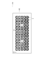
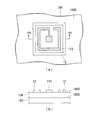
- FIG. 1 It is a top view which shows an example of the printed circuit board by this embodiment of this invention. It is a top view which shows the structural example of the electromagnetic band gap structure 1 in FIG. It is a figure explaining the structure of the stub pattern 112 for 1st frequencies in the electromagnetic band gap structure 11, and the stub pattern 113 for 2nd frequencies of a frequency higher than a 1st frequency. It is sectional drawing of the printed circuit board by which the surface type electromagnetic band gap structure 1 is arrange
- FIG. 1 is a plan view showing an example of a printed circuit board according to this embodiment of the present invention.
- FIG. 1 is a more specific example of the configuration of FIG. 9, which is a conceptual diagram of a basic configuration of an artificial magnetic conductor according to the present invention, which will be described later, corresponding to the following embodiments.
- a power plane (Power Plane) 102 is superposed on one main surface (front surface) of a reference plane (Reference Plane, for example, ground plane) 101.
- the power plane 102 is provided such that the other main surface (back surface) faces the upper surface (front surface) of the reference plane 101.
- the power plane 102 is provided on one main surface (front surface) so that the electromagnetic bandgap structures 1 are arranged in a matrix with a predetermined period.
- the electromagnetic bandgap structure 1 is an electric circuit for electromagnetic noise generated from an electronic circuit (CPU (Central Processing Unit) and memory) disposed on a printed circuit board formed by a reference plane 101 and a power plane 102. Absorb energy. Further, as described above, the printed circuit board may be arranged as a single unit, not a configuration in which a plurality of electromagnetic band gap structures 1 are arranged in a matrix. That is, in order to reduce the propagation of electromagnetic noise on the printed circuit board, the electromagnetic bandgap structure 1 may be disposed only at a position facing the electronic circuit that generates electromagnetic noise, for example, in units of one. You may do it.
- FIG. 2 is a plan view showing a configuration example of the electromagnetic bandgap structure 1 in FIG.
- an electromagnetic band gap structure 1 is a surface type electromagnetic band gap structure formed on an upper portion of one main surface (front surface) of a power plane 102.
- the outer shape of the electromagnetic band gap structure 1 has a length in the X-axis direction of 3.1 mm and a length in the Y-axis direction of 3.1 mm.
- the electromagnetic band gap structure 1 includes an electromagnetic band gap structure 11 and an auxiliary pattern 12.
- the auxiliary pattern 12 has a closed ring shape, for example, and is arranged with a predetermined distance with respect to the outer periphery of the electromagnetic band gap structure 11.
- the auxiliary pattern 12 is provided so as to surround the outer periphery of the electromagnetic band gap structure 11.
- the electromagnetic band gap structure 11 includes a via pattern 111, a low frequency stub pattern 112 (first electromagnetic band gap structure), and a high frequency stub pattern 113 (second electromagnetic band gap structure).
- Each of the stub patterns 112 and 113 constitutes an open stub.
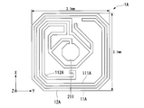
- FIG. 3 is a diagram illustrating the structure of the stub pattern 112 for the first frequency and the stub pattern 113 for the second frequency having a frequency higher than the first frequency in the electromagnetic bandgap structure 11.
- the first frequency is, for example, a frequency (first frequency) of 2.45 GHz in the wireless LAN
- the second frequency is a frequency higher than the first frequency.
- the frequency is 44 GHz (second frequency).
- FIG. 3A shows a portion of the stub pattern 112 for the first frequency that functions as a stub for the first frequency in a hatched pattern.
- the stub pattern 112 is formed as a pattern wired in a bent shape, for example, a folded structure pattern such as a spiral shape and a meander shape in the present embodiment, or a pattern combining a spiral shape and a meander shape. Yes. Further, the stub pattern 112 is formed as an open stub having a transmission line width of 0.1 mm and an overall transmission line length of 19 mm, for example.
- the adjustment stub pattern 112_1 is a transmission line, and has a width of 0.1 mm and a length of 1.37 mm. The adjustment stub pattern 112_2 has a width of 0.1 mm and a length of 1.37 mm.
- Each of the adjustment stub patterns 112_1 and 112_2 described above is a pattern provided so as to extend from a part of the transmission line of the stub pattern 112 as a starting point in order to finely adjust the stub length of the stub pattern 112. You may add or delete as needed.
- the lengths of the adjustment stub patterns 112_1 and 112_2 are set so that the stub length of the stub pattern 112 can be adjusted.
- the stub pattern 112 has an electrical length of about ⁇ / 3.7 with respect to a frequency of 2.45 GHz (a first frequency that is lower than 5.44 GHz described later).
- Z in ⁇ jZ 0 cot ⁇ l
- ⁇ is a phase constant, and is represented by 2 ⁇ / ⁇ where ⁇ is the wavelength of the electromagnetic wave on the stub pattern which is a transmission line.
- l is the physical length (mm) of the stub pattern.
- Z 0 is the characteristic impedance of the open stub (transmission line). Therefore, ⁇ l obtained by multiplying ⁇ and l is the electrical length [rad] of the stub pattern.
- the impedance characteristic of the open stub is an inductive impedance characteristic when the electrical length of the transmission line is between ⁇ / 4 and ⁇ / 2, and the electrical length of the transmission line is shorter than ⁇ / 4.
- the impedance becomes capacitive impedance, and becomes “0” when the electrical length of the transmission line is ⁇ / 4.
- the stub pattern 112 in this figure has an inductive impedance characteristic because the electrical length is about ⁇ / 3.7 at 2.45 GHz and is between ⁇ / 4 and ⁇ / 2, and has an electromagnetic band gap.
- the auxiliary pattern 12 has a ring shape having a predetermined width, for example, and is provided so as to surround the outer periphery of the stub pattern 112.
- the auxiliary pattern 12 has an electrical length of about ⁇ / 6 to ⁇ / 7 at a frequency of 2.45 GHz. For this reason, the auxiliary pattern 12 has a characteristic of capacitive impedance because the electrical length is shorter than ⁇ / 4.
- capacitive coupling is performed with respect to the stub pattern 112.
- the capacitive component of the stub pattern 112 is increased, and the electrical length of the stub pattern 112 can be made longer than about ⁇ / 3.7.
- the stub pattern 112 is shortened and when the prepreg (reinforcing dielectric layer 104 described later) is thinned, an effect of reducing the resonance frequency can be obtained.
- the relationship between the line width W of the stub pattern 112 and the distance L between the stub pattern 112 and the auxiliary pattern 12 is W> L.
- FIG. 3B shows the portion of the stub pattern 113 for the second frequency, which functions as a stub for the second frequency, with a hatched pattern.
- the stub pattern 113 is formed as a spiral pattern, a folded pattern such as a meander shape, or a meandering pattern combining the spiral shape and the meander shape as shown in FIG. ing.
- the stub pattern 113 is formed as an open stub having a transmission line width of 0.1 mm, for example, and an overall length of the transmission line of 8.9 mm.
- the stub pattern 113 has an electrical length of about ⁇ as in the stub pattern 112 with respect to a frequency of 5.44 GHz (second frequency that is higher than 2.45 GHz described above). /3.7.
- the stub pattern 113 has an inductive impedance and forms an electromagnetic band gap structure.
- the resonance frequency is set only by the length of the pattern as the transmission path.
- FIG. 4 is a cross-sectional view of a printed circuit board on which the surface type electromagnetic band gap structure 1 is arranged.
- FIG. 4 shows a cross section when the printed circuit board in FIG. 1 is cut along line IV-IV.
- a reference plane 101 having a thickness of 35 ⁇ m made of, for example, copper is disposed as a conductor layer of metal or the like.
- the core substrate 103 is a substrate having a thickness of 0.4 mm made of, for example, glass epoxy having a dielectric constant of 4.3.
- a power plane 102 (Power Plane) having a thickness of 35 ⁇ m and made of, for example, copper is disposed as a conductor layer of metal or the like.
- the surface of the substrate or the like facing the upper direction of the drawing is referred to as the upper surface, and the surface facing the lower direction of the drawing is described as the lower surface.
- a reinforcing dielectric layer 104 (prepreg) having a thickness of 0.2 mm made of glass epoxy having a dielectric constant of 4.3 is disposed.
- the electromagnetic band gap structure 1 is formed as a conductor layer of metal or the like with a thickness of 35 ⁇ m made of, for example, copper.
- a layer of a soldering resist 150 having a thickness of 0.05 mm is formed on the exposed upper surface of the reinforcing dielectric layer 104 and the upper surface of the electromagnetic band gap structure 1.
- the via pattern 111 is connected to the reference plane 101 via a via hole 160 having a diameter of 0.3 mm.
- a pattern 210 in the power supply plane 102 is formed below the electromagnetic band gap structure 11 and the auxiliary pattern 12 in the electromagnetic band gap structure 1 with a reinforcing dielectric layer 104 interposed therebetween.
- the distance R between the electromagnetic band gap structures 1 adjacent in the horizontal direction is, for example, 2 mm.
- the electromagnetic band gap structure 1 is provided as a surface type on the upper surface of the reinforcing dielectric layer 104. Since the electromagnetic bandgap structure 1 is observed through the soldering resist 150, the electromagnetic bandgap structure 1 formed on the upper surface of the reinforcing dielectric layer 104 is a surface type.
- the electromagnetic noise corresponding to the resonance frequency of the electromagnetic bandgap structure 11 among the electromagnetic noise generated from the electronic component is printed circuit board 101. Suppresses propagation inside.
- the frequencies of the stub pattern 112 and the stub pattern 113 are 2.45 GHz and 5.44 GHz, respectively. Suppress propagation.
- the influence of electromagnetic noise on the analog circuit of the wireless LAN arranged on the same substrate is reduced, interference of electromagnetic noise with respect to data transmission / reception in the wireless LAN can be suppressed.
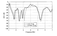
- FIG. 5 is a graph showing the correspondence between the frequency and the S parameter (insertion loss S 21 ) of the electromagnetic bandgap structure 1 (surface type).
- the horizontal axis represents the frequency
- the vertical axis represents the insertion loss S 21.
- the broken line indicates the correspondence between the frequency of the electromagnetic band gap structure 1 (that is, the electromagnetic band gap structure 11) and the insertion loss S 21 when the auxiliary pattern 12 is not provided on the outer periphery of the electromagnetic band gap structure 11.
- it shows the correspondence between the frequency of the electromagnetic bandgap structure 1 and the insertion loss S 21 in the case where the solid line is an auxiliary pattern 12 on the outer periphery of EBG structure 11.
- FIG. 6 is a cross-sectional view of a printed circuit board on which the interior type electromagnetic bandgap structure 1A is arranged.
- the surface of the substrate or the like facing the upper direction of the drawing is referred to as the upper surface
- the surface facing the lower direction of the drawing is described as the lower surface.
- a reference plane 101 having a thickness of 35 ⁇ m made of, for example, copper is disposed as a conductor layer of metal or the like.
- an electromagnetic band gap layer 105 made up of a plurality of electromagnetic band gap structures 1 formed in a pattern having a thickness of 35 ⁇ m made of copper, for example, as a conductor layer of metal or the like.
- a reinforcing dielectric layer 104 is formed on the upper surface of the electromagnetic band gap layer 105.
- a power plane 102 is formed on the top surface of the reinforced dielectric layer 104.
- a soldering resist 150 is formed on the upper surface of the power plane 102 and the exposed upper surface of the reinforcing dielectric layer 104.
- the via pattern 211 is connected to the reference plane 101 via a via hole 170 having a diameter of 0.3 mm, for example.
- a pattern 220 in the power supply plane 102 is formed above the electromagnetic band gap structure 11A and the auxiliary pattern 12A in the electromagnetic band gap structure 1A via the reinforcing dielectric layer 104. Further, the distance R between the adjacent electromagnetic band gap structures 1A in the horizontal direction is 0.2 mm as in the above-described embodiment.
- the electromagnetic band gap structure 1 ⁇ / b> A is provided as an interior type between the reinforcing dielectric layer 104 and the core substrate 103.
- FIG. 7 is a plan view showing a configuration example of an electromagnetic bandgap structure 1A used for the inner layer type in FIG.
- an electromagnetic band gap structure 1 ⁇ / b> A is a surface type electromagnetic band gap structure formed on the upper surface of the core substrate 103.
- the outer shape of the electromagnetic band gap structure 1A has a length in the X-axis direction of 3.1 mm and a length in the Y-axis direction of 3.1 mm.
- the electromagnetic bandgap structure 1A includes an electromagnetic bandgap structure 11A and an auxiliary pattern 12A.
- the auxiliary pattern 12A has, for example, a closed ring shape, and is arranged with a predetermined distance with respect to the outer periphery of the electromagnetic band gap structure 11A.
- the auxiliary pattern 12A is provided so as to surround the outer periphery of the electromagnetic band gap structure 11A.
- the electromagnetic band gap structure 11A includes a via pattern 211, a stub pattern 112A for the first frequency, and a stub pattern 113A for the second frequency. Each of the stub patterns 112A and 113A constitutes an open stub.
- the interior type electromagnetic band gap structure 1 ⁇ / b> A has the stub length of each of the stub patterns 112 ⁇ / b> A and 113 ⁇ / b> A adjusted by the difference in electrical length, and the basic structure is the same as that of the surface type electromagnetic band gap structure 1.
- the electromagnetic band gap structure 11 ⁇ / b> A is formed on one main surface (surface) of the core substrate 103.
- the reinforcing dielectric layer 104 is formed on an upper part of the arranged surface of the electromagnetic band gap structure 11A. That is, the electromagnetic band gap structure 11 ⁇ / b> A is formed between the core substrate 103 and the reinforcing dielectric layer 104. For this reason, the electromagnetic band gap structure 11A is defined as an interior type in the present embodiment.
- FIG. 8 is a graph showing the correspondence between the frequency and the S parameter (insertion loss S 21 ) of the electromagnetic band gap structure 1A (interior type). 8, the horizontal axis represents frequency and the vertical axis represents the insertion loss S 21. Further, in FIG. 8 shows the correspondence between the frequency of the electromagnetic bandgap structure 1A (i.e. EBG structure 11A) and the insertion loss S 21 in the case where the broken line is not provided an auxiliary pattern 12A on the outer periphery of EBG structures 11A ing. On the other hand, it shows the correspondence between the frequency of the electromagnetic bandgap structures 1A and insertion loss S 21 in the case where the solid line is an auxiliary pattern 12A on the outer periphery of EBG structure 11A.
- the stub pattern 112 (112A) in the electromagnetic bandgap structure 11 (11A) is loaded with the auxiliary pattern 12 (12A), and the resonance frequency of the electromagnetic bandgap structure 11 is set. Therefore, the electromagnetic band gap structure 1 can be reduced in size as compared with the conventional case where the resonance frequency is lowered by increasing the length of the outer periphery of the electromagnetic band gap structure 11 (11A). Is possible. For example, in the case of the configuration similar to the present embodiment, if the auxiliary pattern 12 is not formed along the outer periphery of the electromagnetic band gap structure 11, the size of the electromagnetic band gap structure is 3.5 mm ⁇ 3.5 mm. .
- the electromagnetic bandgap structure 1 in the present embodiment is 3.1 mm ⁇ 3.1 mm, it is 78% larger than the 3.5 mm ⁇ 3.5 mm size when the auxiliary pattern 12 is not provided. The size of the electromagnetic band gap structure can be reduced.
- the electromagnetic field strength can be suppressed by using the electromagnetic band gap structure 1 (1A).
- the radiated electromagnetic field strength at 2.45 GHz on the low frequency side is 1.13 ( ⁇ W)
- the radiated electromagnetic field strength at 5.44 GHz on the high frequency side is 57.2 ( ⁇ W).
- the radiation electromagnetic field strength at 2.45 GHz on the low frequency side is 0.0609 ( ⁇ W)
- the radiation at 5.44 GHz on the high frequency side is 0.252 ( ⁇ W).
- the radiated electromagnetic field intensity at 2.45 GHz on the low frequency side is 0.00475 ( ⁇ W)
- the radiated electromagnetic field at 5.44 GHz on the high frequency side is 0.201 ( ⁇ W).
- the stub pattern 112 (112A) in the electromagnetic band gap 11 (11A) is formed so as to be surrounded by the auxiliary pattern 12 (12A).
- the electromagnetic bandgap structure 11 (11A) can be reduced in size as compared with the configuration in which the resonance frequency is lowered by increasing the length, and the mounting space can be effectively utilized.
- the auxiliary pattern 12 (12A) is not a closed ring pattern but an open ring pattern, and has a length that reduces the resonance frequency of the electromagnetic bandgap structure 1 to a target frequency and has a capacitive impedance characteristic. If it is good. Further, the auxiliary pattern 12 may be a linear pattern disposed at a position where the auxiliary pattern 12 is capacitively coupled to the outer peripheral side of the electromagnetic bandgap structure 11 (11A) as long as it has a capacity impedance characteristic. An open via may be provided for the auxiliary pattern 12 (12A) to increase the capacitance.
- the pattern of the auxiliary pattern 12 (12A) may be divided into a plurality of elements, and the elements may be connected to each other by a gap capacitance, a capacitor, or a resistor. Furthermore, an insulating layer is provided on the electromagnetic bandgap structure 11 (11A), and a stub pattern 112 (112A) auxiliary pattern is formed on the insulating layer in plan view, thereby shifting the frequency to the low frequency side. be able to. Thereby, according to this embodiment, since the size of the electromagnetic band gap structure 11 (11A) can be further reduced, the mounting space can be effectively utilized.
- FIG. 9 is a diagram showing the concept of the printed circuit board of the present invention.
- FIG. 9A shows a stub pattern 113 (first electromagnetic band) on the surface 104S (one surface of the reinforcing dielectric layer) of the reinforcing dielectric layer 104 (reinforcing dielectric layer) in plan view.
- a printed circuit board on which patterns of a gap structure) and an auxiliary pattern 12 (auxiliary pattern) are wired is shown.
- FIG. 9B shows a cross section taken along line IXB-IXB in the printed circuit board of FIG. 9A. As shown in FIG.
- a stub pattern 113 (first electromagnetic band gap structure) is formed on the surface 104S (any one surface of the reinforcing dielectric layer) of the reinforcing dielectric layer 104 (reinforcing dielectric layer). ) And the auxiliary pattern 12 (auxiliary pattern).
- the auxiliary pattern 12 (auxiliary pattern) is formed with a predetermined distance from the outer periphery of the stub pattern 113 (first electromagnetic band gap structure). This auxiliary pattern 12 (auxiliary pattern) is provided for capacitive loading to the stub pattern 113 (first electromagnetic band gap structure) in order to lower the resonance frequency of the stub pattern 113 (first electromagnetic band gap structure). It has been.
- a reinforcing dielectric layer 104 (reinforcing dielectric layer) is provided on the surface 103S (any one surface of the core substrate) of the core substrate 103 (core substrate).
- a stub pattern 113 first electromagnetic band gap structure
- an auxiliary pattern 12 auxiliary pattern
- a surface 104S any one surface of the reinforcing dielectric layer of the reinforcing dielectric layer 104 (reinforcing dielectric layer)
- Each pattern is formed.
- the auxiliary pattern 12 is loaded with capacity on the stub pattern 113 (first electromagnetic band gap structure) to reduce the resonance frequency of the stub pattern 113 (first electromagnetic band gap structure).
- the stub pattern 113 first electromagnetic band gap structure
- the stub pattern 113 (first electromagnetic band gap structure) can be reduced in size compared with the case where the resonance frequency is lowered by increasing the length of the outer periphery of the circuit board, and effective use of the mounting space on the printed circuit board can be achieved. It can be carried out.
- This embodiment has been described by taking a printed circuit board as an example, but can also be applied to a circuit board having no printed pattern.
Landscapes
- Engineering & Computer Science (AREA)
- Microelectronics & Electronic Packaging (AREA)
- Physics & Mathematics (AREA)
- Electromagnetism (AREA)
- Structure Of Printed Boards (AREA)
- Parts Printed On Printed Circuit Boards (AREA)
- Production Of Multi-Layered Print Wiring Board (AREA)
- Shielding Devices Or Components To Electric Or Magnetic Fields (AREA)
Priority Applications (2)
| Application Number | Priority Date | Filing Date | Title |
|---|---|---|---|
| CN201580031404.XA CN106465551B (zh) | 2014-06-12 | 2015-06-12 | 电路基板以及电路基板的减噪方法 |
| US15/317,437 US10111318B2 (en) | 2014-06-12 | 2015-06-12 | Circuit substrate, and noise reduction method for circuit substrate |
Applications Claiming Priority (2)
| Application Number | Priority Date | Filing Date | Title |
|---|---|---|---|
| JP2014-121596 | 2014-06-12 | ||
| JP2014121596A JP5929969B2 (ja) | 2014-06-12 | 2014-06-12 | プリント回路基板及びプリント回路基板におけるノイズ低減方法 |
Publications (1)
| Publication Number | Publication Date |
|---|---|
| WO2015190610A1 true WO2015190610A1 (ja) | 2015-12-17 |
Family
ID=54833693
Family Applications (1)
| Application Number | Title | Priority Date | Filing Date |
|---|---|---|---|
| PCT/JP2015/067090 Ceased WO2015190610A1 (ja) | 2014-06-12 | 2015-06-12 | 回路基板及び回路基板におけるノイズ低減方法 |
Country Status (4)
| Country | Link |
|---|---|
| US (1) | US10111318B2 (https=) |
| JP (1) | JP5929969B2 (https=) |
| CN (1) | CN106465551B (https=) |
| WO (1) | WO2015190610A1 (https=) |
Cited By (1)
| Publication number | Priority date | Publication date | Assignee | Title |
|---|---|---|---|---|
| US12573735B2 (en) | 2021-09-29 | 2026-03-10 | Panasonic Intellectual Property Management Co., Ltd. | Multilayer device |
Families Citing this family (3)
| Publication number | Priority date | Publication date | Assignee | Title |
|---|---|---|---|---|
| JP6611065B2 (ja) * | 2016-07-27 | 2019-11-27 | 国立大学法人 岡山大学 | 印刷配線板 |
| JP6744201B2 (ja) * | 2016-11-28 | 2020-08-19 | 京セラ株式会社 | 印刷配線板 |
| KR101867856B1 (ko) * | 2017-06-07 | 2018-06-15 | 엘지전자 주식회사 | 전자파 장해 감쇄 장치 및 이를 구비하는 홈 어플라이언스 |
Citations (2)
| Publication number | Priority date | Publication date | Assignee | Title |
|---|---|---|---|---|
| JP2010010183A (ja) * | 2008-06-24 | 2010-01-14 | Nec Corp | 導波路構造およびプリント配線板 |
| JP2010252329A (ja) * | 2009-04-15 | 2010-11-04 | Internatl Business Mach Corp <Ibm> | 切換可能なオンチップ遅波伝送線路帯域消去フィルタのための回路構造体及び設計構造体並びに製造方法 |
Family Cites Families (14)
| Publication number | Priority date | Publication date | Assignee | Title |
|---|---|---|---|---|
| JP2735060B2 (ja) * | 1995-12-27 | 1998-04-02 | 日本電気株式会社 | プリント回路基板およびプリント回路基板の設計方法およびプリント回路基板作製装置 |
| US7215007B2 (en) | 2003-06-09 | 2007-05-08 | Wemtec, Inc. | Circuit and method for suppression of electromagnetic coupling and switching noise in multilayer printed circuit boards |
| US7148425B2 (en) * | 2004-01-29 | 2006-12-12 | National Sun Yat-Sen University | Power plane system of high-speed digital circuit for suppressing ground bounce noise |
| US7136028B2 (en) | 2004-08-27 | 2006-11-14 | Freescale Semiconductor, Inc. | Applications of a high impedance surface |
| US7760140B2 (en) | 2006-06-09 | 2010-07-20 | Intel Corporation | Multiband antenna array using electromagnetic bandgap structures |
| JP2008004853A (ja) | 2006-06-26 | 2008-01-10 | Hitachi Ltd | 積層半導体装置およびモジュール |
| KR100999550B1 (ko) * | 2008-10-08 | 2010-12-08 | 삼성전기주식회사 | 전자기 밴드갭 구조물 |
| FI124128B (fi) * | 2008-10-28 | 2014-03-31 | Tellabs Oy | Suodatinrakenne |
| WO2010125784A1 (ja) * | 2009-04-30 | 2010-11-04 | 日本電気株式会社 | 構造体、プリント基板、アンテナ、伝送線路導波管変換器、アレイアンテナ、電子装置 |
| US9350078B2 (en) * | 2009-12-04 | 2016-05-24 | Nec Corporation | Structural body, printed substrate, antenna, transmission line waveguide converter, array antenna, and electronic device |
| CN102497729A (zh) * | 2011-12-07 | 2012-06-13 | 苏州日月明微电子科技有限公司 | 一种电磁带隙结构 |
| JP2013153041A (ja) | 2012-01-25 | 2013-08-08 | Nec Tokin Corp | ノイズ抑制構造体 |
| TWI565400B (zh) * | 2014-07-01 | 2017-01-01 | 華碩電腦股份有限公司 | 電磁帶隙結構與具有電磁帶隙結構的電子裝置 |
| JP6593350B2 (ja) * | 2015-02-12 | 2019-10-23 | 日本電気株式会社 | 構造体および配線基板 |
-
2014
- 2014-06-12 JP JP2014121596A patent/JP5929969B2/ja not_active Expired - Fee Related
-
2015
- 2015-06-12 US US15/317,437 patent/US10111318B2/en active Active
- 2015-06-12 CN CN201580031404.XA patent/CN106465551B/zh active Active
- 2015-06-12 WO PCT/JP2015/067090 patent/WO2015190610A1/ja not_active Ceased
Patent Citations (2)
| Publication number | Priority date | Publication date | Assignee | Title |
|---|---|---|---|---|
| JP2010010183A (ja) * | 2008-06-24 | 2010-01-14 | Nec Corp | 導波路構造およびプリント配線板 |
| JP2010252329A (ja) * | 2009-04-15 | 2010-11-04 | Internatl Business Mach Corp <Ibm> | 切換可能なオンチップ遅波伝送線路帯域消去フィルタのための回路構造体及び設計構造体並びに製造方法 |
Cited By (1)
| Publication number | Priority date | Publication date | Assignee | Title |
|---|---|---|---|---|
| US12573735B2 (en) | 2021-09-29 | 2026-03-10 | Panasonic Intellectual Property Management Co., Ltd. | Multilayer device |
Also Published As
| Publication number | Publication date |
|---|---|
| CN106465551A (zh) | 2017-02-22 |
| US10111318B2 (en) | 2018-10-23 |
| CN106465551B (zh) | 2019-01-18 |
| JP5929969B2 (ja) | 2016-06-08 |
| JP2016001691A (ja) | 2016-01-07 |
| US20170127510A1 (en) | 2017-05-04 |
Similar Documents
| Publication | Publication Date | Title |
|---|---|---|
| JP5533860B2 (ja) | 構造体、プリント基板、アンテナ、伝送線路導波管変換器、アレイアンテナ、電子装置 | |
| JP5931851B2 (ja) | ノイズ抑制構造を有する回路基板 | |
| JP5550100B2 (ja) | 電磁バンドギャップ素子及びそれを用いたアンテナ並びにフィルタ | |
| JP5670251B2 (ja) | コモンモードノイズ抑制回路 | |
| JP5726983B2 (ja) | チップ状アンテナ装置及び送受信用通信回路基板 | |
| WO2002091515A1 (fr) | Composantes de type ligne de transmission | |
| JP2017041879A (ja) | 放射パターン同士間の干渉を低減したアンテナシステムおよびアンテナモジュール | |
| CN112544015B (zh) | 波导管缝隙天线 | |
| US9629282B2 (en) | Electronic device, structure, and heat sink | |
| JP5929969B2 (ja) | プリント回路基板及びプリント回路基板におけるノイズ低減方法 | |
| JP2016134809A (ja) | 構造体及び電子回路 | |
| WO2015122203A1 (ja) | プリント基板 | |
| US20150222003A1 (en) | Microwave circuit | |
| JP6249648B2 (ja) | プリント回路板及び電子機器 | |
| TWI626793B (zh) | 抗電磁干擾單元 | |
| JP5994108B2 (ja) | コモンモードノイズフィルタ | |
| JP2001068801A (ja) | プリント配線板 | |
| JP2008205403A (ja) | 集積回路 | |
| JP5082250B2 (ja) | 高周波回路基板 | |
| WO2014136595A1 (ja) | 構造体、配線基板及び電子装置 | |
| CN107896420A (zh) | 电路板及其电磁带隙结构 | |
| CN111602289B (zh) | 天线和通信设备 | |
| JP2014103591A (ja) | 平面アンテナ | |
| JP2010171290A (ja) | 電子回路モジュール | |
| JP2016127511A (ja) | 導波路変換構造体 |
Legal Events
| Date | Code | Title | Description |
|---|---|---|---|
| 121 | Ep: the epo has been informed by wipo that ep was designated in this application |
Ref document number: 15806207 Country of ref document: EP Kind code of ref document: A1 |
|
| WWE | Wipo information: entry into national phase |
Ref document number: 15317437 Country of ref document: US |
|
| NENP | Non-entry into the national phase |
Ref country code: DE |
|
| 122 | Ep: pct application non-entry in european phase |
Ref document number: 15806207 Country of ref document: EP Kind code of ref document: A1 |