WO2015166647A1 - 有機発光デバイスの機能層の形成方法及び有機発光デバイスの製造方法 - Google Patents
有機発光デバイスの機能層の形成方法及び有機発光デバイスの製造方法 Download PDFInfo
- Publication number
- WO2015166647A1 WO2015166647A1 PCT/JP2015/002178 JP2015002178W WO2015166647A1 WO 2015166647 A1 WO2015166647 A1 WO 2015166647A1 JP 2015002178 W JP2015002178 W JP 2015002178W WO 2015166647 A1 WO2015166647 A1 WO 2015166647A1
- Authority
- WO
- WIPO (PCT)
- Prior art keywords
- ink
- groove
- solvent
- layer
- groove region
- Prior art date
- Legal status (The legal status is an assumption and is not a legal conclusion. Google has not performed a legal analysis and makes no representation as to the accuracy of the status listed.)
- Ceased
Links
Images





Classifications
-
- H—ELECTRICITY
- H05—ELECTRIC TECHNIQUES NOT OTHERWISE PROVIDED FOR
- H05B—ELECTRIC HEATING; ELECTRIC LIGHT SOURCES NOT OTHERWISE PROVIDED FOR; CIRCUIT ARRANGEMENTS FOR ELECTRIC LIGHT SOURCES, IN GENERAL
- H05B33/00—Electroluminescent light sources
- H05B33/10—Apparatus or processes specially adapted to the manufacture of electroluminescent light sources
-
- B—PERFORMING OPERATIONS; TRANSPORTING
- B41—PRINTING; LINING MACHINES; TYPEWRITERS; STAMPS
- B41J—TYPEWRITERS; SELECTIVE PRINTING MECHANISMS, i.e. MECHANISMS PRINTING OTHERWISE THAN FROM A FORME; CORRECTION OF TYPOGRAPHICAL ERRORS
- B41J2/00—Typewriters or selective printing mechanisms characterised by the printing or marking process for which they are designed
- B41J2/005—Typewriters or selective printing mechanisms characterised by the printing or marking process for which they are designed characterised by bringing liquid or particles selectively into contact with a printing material
- B41J2/01—Ink jet
- B41J2/21—Ink jet for multi-colour printing
-
- H—ELECTRICITY
- H05—ELECTRIC TECHNIQUES NOT OTHERWISE PROVIDED FOR
- H05B—ELECTRIC HEATING; ELECTRIC LIGHT SOURCES NOT OTHERWISE PROVIDED FOR; CIRCUIT ARRANGEMENTS FOR ELECTRIC LIGHT SOURCES, IN GENERAL
- H05B33/00—Electroluminescent light sources
- H05B33/12—Light sources with substantially two-dimensional [2D] radiating surfaces
-
- H—ELECTRICITY
- H05—ELECTRIC TECHNIQUES NOT OTHERWISE PROVIDED FOR
- H05B—ELECTRIC HEATING; ELECTRIC LIGHT SOURCES NOT OTHERWISE PROVIDED FOR; CIRCUIT ARRANGEMENTS FOR ELECTRIC LIGHT SOURCES, IN GENERAL
- H05B33/00—Electroluminescent light sources
- H05B33/12—Light sources with substantially two-dimensional [2D] radiating surfaces
- H05B33/22—Light sources with substantially two-dimensional [2D] radiating surfaces characterised by the chemical or physical composition or the arrangement of auxiliary dielectric or reflective layers
-
- H—ELECTRICITY
- H10—SEMICONDUCTOR DEVICES; ELECTRIC SOLID-STATE DEVICES NOT OTHERWISE PROVIDED FOR
- H10K—ORGANIC ELECTRIC SOLID-STATE DEVICES
- H10K50/00—Organic light-emitting devices
-
- H—ELECTRICITY
- H10—SEMICONDUCTOR DEVICES; ELECTRIC SOLID-STATE DEVICES NOT OTHERWISE PROVIDED FOR
- H10K—ORGANIC ELECTRIC SOLID-STATE DEVICES
- H10K50/00—Organic light-emitting devices
- H10K50/10—OLEDs or polymer light-emitting diodes [PLED]
- H10K50/14—Carrier transporting layers
- H10K50/15—Hole transporting layers
-
- H—ELECTRICITY
- H10—SEMICONDUCTOR DEVICES; ELECTRIC SOLID-STATE DEVICES NOT OTHERWISE PROVIDED FOR
- H10K—ORGANIC ELECTRIC SOLID-STATE DEVICES
- H10K50/00—Organic light-emitting devices
- H10K50/10—OLEDs or polymer light-emitting diodes [PLED]
- H10K50/14—Carrier transporting layers
- H10K50/16—Electron transporting layers
-
- H—ELECTRICITY
- H10—SEMICONDUCTOR DEVICES; ELECTRIC SOLID-STATE DEVICES NOT OTHERWISE PROVIDED FOR
- H10K—ORGANIC ELECTRIC SOLID-STATE DEVICES
- H10K59/00—Integrated devices, or assemblies of multiple devices, comprising at least one organic light-emitting element covered by group H10K50/00
- H10K59/10—OLED displays
- H10K59/12—Active-matrix OLED [AMOLED] displays
- H10K59/122—Pixel-defining structures or layers, e.g. banks
-
- H—ELECTRICITY
- H10—SEMICONDUCTOR DEVICES; ELECTRIC SOLID-STATE DEVICES NOT OTHERWISE PROVIDED FOR
- H10K—ORGANIC ELECTRIC SOLID-STATE DEVICES
- H10K59/00—Integrated devices, or assemblies of multiple devices, comprising at least one organic light-emitting element covered by group H10K50/00
- H10K59/30—Devices specially adapted for multicolour light emission
- H10K59/35—Devices specially adapted for multicolour light emission comprising red-green-blue [RGB] subpixels
-
- H—ELECTRICITY
- H10—SEMICONDUCTOR DEVICES; ELECTRIC SOLID-STATE DEVICES NOT OTHERWISE PROVIDED FOR
- H10K—ORGANIC ELECTRIC SOLID-STATE DEVICES
- H10K71/00—Manufacture or treatment specially adapted for the organic devices covered by this subclass
-
- H—ELECTRICITY
- H10—SEMICONDUCTOR DEVICES; ELECTRIC SOLID-STATE DEVICES NOT OTHERWISE PROVIDED FOR
- H10K—ORGANIC ELECTRIC SOLID-STATE DEVICES
- H10K71/00—Manufacture or treatment specially adapted for the organic devices covered by this subclass
- H10K71/10—Deposition of organic active material
- H10K71/12—Deposition of organic active material using liquid deposition, e.g. spin coating
- H10K71/13—Deposition of organic active material using liquid deposition, e.g. spin coating using printing techniques, e.g. ink-jet printing or screen printing
- H10K71/135—Deposition of organic active material using liquid deposition, e.g. spin coating using printing techniques, e.g. ink-jet printing or screen printing using ink-jet printing
-
- H—ELECTRICITY
- H10—SEMICONDUCTOR DEVICES; ELECTRIC SOLID-STATE DEVICES NOT OTHERWISE PROVIDED FOR
- H10K—ORGANIC ELECTRIC SOLID-STATE DEVICES
- H10K50/00—Organic light-emitting devices
- H10K50/10—OLEDs or polymer light-emitting diodes [PLED]
- H10K50/17—Carrier injection layers
-
- H—ELECTRICITY
- H10—SEMICONDUCTOR DEVICES; ELECTRIC SOLID-STATE DEVICES NOT OTHERWISE PROVIDED FOR
- H10K—ORGANIC ELECTRIC SOLID-STATE DEVICES
- H10K50/00—Organic light-emitting devices
- H10K50/80—Constructional details
- H10K50/86—Arrangements for improving contrast, e.g. preventing reflection of ambient light
- H10K50/865—Arrangements for improving contrast, e.g. preventing reflection of ambient light comprising light absorbing layers, e.g. light-blocking layers
-
- H—ELECTRICITY
- H10—SEMICONDUCTOR DEVICES; ELECTRIC SOLID-STATE DEVICES NOT OTHERWISE PROVIDED FOR
- H10K—ORGANIC ELECTRIC SOLID-STATE DEVICES
- H10K59/00—Integrated devices, or assemblies of multiple devices, comprising at least one organic light-emitting element covered by group H10K50/00
- H10K59/30—Devices specially adapted for multicolour light emission
- H10K59/38—Devices specially adapted for multicolour light emission comprising colour filters or colour changing media [CCM]
Definitions
- the present invention relates to a forming method for forming a functional layer in an organic light emitting device, and more particularly, to a method for forming a functional layer by applying ink to a region partitioned by a bank.
- an organic EL device in which a plurality of organic EL elements are arranged in a matrix in a vertical direction and a horizontal direction on a substrate has been put into practical use.
- This organic EL device has high visibility because each organic EL element emits light, and is excellent in impact resistance because it is a complete solid element.
- each organic EL element has a basic structure in which a light emitting layer containing an organic light emitting material is disposed between a pair of electrodes of an anode and a cathode, and a voltage is applied between the pair of electrodes during driving. Is applied, and light is emitted along with recombination of holes injected from the anode into the light emitting layer and electrons injected from the cathode into the light emitting layer.
- an organic EL device for full-color display such an organic EL element forms RGB subpixels, and adjacent RGB subpixels are combined to form one pixel.
- an organic EL device In an organic EL device, generally, a light emitting layer of each organic EL element and a light emitting layer of an adjacent organic EL element are partitioned by a bank made of an insulating material. Further, an organic layer such as a hole injection layer, a hole transport layer, or a hole injection / transport layer is interposed between the anode and the light emitting layer as necessary, and also between the cathode and the light emitting layer as necessary. An electron injection layer, an electron transport layer, or an electron injection / transport layer is interposed. These hole injection layer, hole transport layer, hole injection / transport layer, electron injection layer, electron transport layer, electron injection / transport layer, and the like are collectively referred to as a functional layer.
- Patent Document 1 When manufacturing such an organic EL device, as shown in Patent Document 1, a plurality of banks extending in one direction are formed on a substrate, and a functional layer is formed in each groove region partitioned by the banks. There is a process to do.
- a wet method in which an ink for forming a light emitting layer containing a polymer material or a low molecule having a good thin film formability is applied to a concave space by an inkjet method or the like is often used. According to this wet method, the light emitting layer can be formed relatively easily even in a large panel.
- the amount of ink applied may be different for each groove area.
- the amount of ink applied to these groove regions is also different.
- each groove region is dried during drying.
- the drying speed is uneven for each place, and as a result, the thickness distribution of the functional layer formed in the groove region may be unevenly formed.
- the thickness distribution of the functional layer is unevenly formed in each groove region, when driving the organic EL device, the current density flowing in a portion having a small film thickness in the groove region is increased, which causes deterioration. It becomes.
- the present invention provides an adjacent groove in which sub-pixels of different colors constituting a pixel are formed when a functional layer is formed by applying ink to a groove region partitioned by a plurality of banks.
- An object is to make the film thickness distribution of the functional layer formed in each groove region uniform even when the amount of ink applied to the region is different.
- a method for forming a functional layer of an organic light emitting device comprising: forming a substrate with a bank having a base substrate and a plurality of banks extending in one direction along the surface of the base substrate and parallel to each other; An organic light emitting device in which a plurality of pixels composed of a plurality of adjacent subpixels having different colors are arranged by applying ink to each groove region between a plurality of banks and drying the applied ink layer
- the formation method for forming the functional layer there are a plurality of groove region groups including a plurality of adjacent groove regions in which sub-pixels having different colors are formed in the banked substrate, and in each groove region group, Some groove areas are set to have a smaller ink application amount per unit area than the remaining groove areas, and some groove areas before or after applying ink to each of the plurality of groove areas.
- a functional layer was formed by applying a solvent and drying the ink layer formed in each of the plurality of groove regions by applying the ink and the solvent.
- unit area refers to the unit area of the opening in the groove region.
- some of the groove regions have a smaller ink application amount per unit area than the remaining groove regions. Is set.
- the solvent application amount per unit area for a part of the groove region where the ink application amount per unit area is small is set larger than the solvent application amount per unit area for the remaining groove regions. Therefore, the coating amount per unit area including the ink and the solvent and the surface area of the ink layer are made uniform between some of the groove regions and the remaining groove regions.
- the ink and the solvent are applied to the plurality of groove regions constituting each groove region group even though the ink application amount per unit area is different between some groove regions and the remaining groove regions.
- the surface area of the ink layer (surface area of the ink layer per groove area unit area) is made uniform. As a result, unevenness in the distribution of the solvent vapor pressure formed above these groove regions during drying is suppressed. In addition, the time required for drying the ink layers formed in the plurality of groove regions constituting each groove region group is made uniform.
- FIG. 1 is a schematic block diagram illustrating a schematic configuration of an organic EL display device 1 according to Embodiment 1.
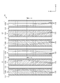
- FIG. 3 is a schematic plan view showing an arrangement form of light emitting elements 11a, 11b, and 11c in the display panel 10.
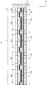
- FIG. 3 is a schematic cross-sectional view showing an AA cross section of FIG. 2.
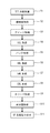
- 3 is a process diagram showing a manufacturing process of the display panel 10.
- FIG. It is a schematic perspective view of the board
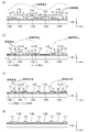
- (A) to (e) are diagrams showing a manufacturing process of the hole transport layer 116 according to Embodiment 1, (a) shows a process of applying a solvent, and (b) shows a process of applying an ink.
- FIG. 1 shows the step of forming the ink layer
- (d) shows the step of drying the ink layer
- (e) shows the state after completion of the hole transport layer.
- A)-(d) is a figure which shows the manufacturing method of the hole transport layer 116 which concerns on a comparative example, (a) shows the state immediately after ink application, (b) shows the state immediately after formation of the hole transport layer 116B.
- (C) shows the state immediately after the formation of the hole transport layer 116G, and (d) shows the state immediately after the formation of the hole transport layer 116R.
- 3 is a diagram schematically showing a cross section of an ink layer 116a formed in a groove region between banks 112.
- FIG. 6 is a schematic plan view showing an arrangement form of light emitting elements 11a, 11b, and 11c in a display panel 20 according to Embodiment 2.
- FIG. FIG. 10 is a schematic cross-sectional view showing an AA cross section of FIG. 9.
- (A) to (e) are diagrams showing a manufacturing process of the hole transport layer 116 according to Embodiment 2, wherein (a) shows a process of applying a solvent, and (b) shows a process of applying an ink.
- C) shows the step of forming the ink layer, (d) shows the step of drying the ink layer, and (e) shows the state after completion of the hole transport layer.
- (A), (b) is a top view of the display panel 30 which concerns on Embodiment 3, (a) shows the example whose opening width of a blue groove area
- the inventor has studied the manufacture of an organic light emitting device in which subpixels are formed in a plurality of groove regions partitioned by a plurality of banks along the surface of the base substrate. As a result of this study, the present inventor found that when the functional layer was formed by applying ink to each groove region during the manufacture of the organic light emitting device, the amount of ink applied was different for each groove region. It has been found that the thickness distribution of the functional layer formed in each groove region is biased.
- the evaporation rate of the solvent is different for each groove region in the drying process.
- an ink flow occurs in a groove region having a low evaporation rate, as known as a coffee stain phenomenon.
- the functional material moves in the ink layer along with the flow of the ink, thereby causing a deviation in the shape of the functional layer after drying.
- the ink layer is dried as uniformly as possible between the groove regions.
- a method for eliminating the uneven thickness of the functional layer formed in each groove region was studied.
- the ink layer can be uniformly dried.
- the amount of ink applied per unit area of the plurality of groove regions can be set to be equal, the ink layer can be uniformly dried.
- the film thickness is set to be different for each groove area, it is necessary to individually set the amount of ink to be applied. It cannot be a quantity.
- a method for forming a functional layer of an organic light-emitting device provides a banked substrate having a base substrate and a plurality of banks extending in one direction along the surface of the base substrate and parallel to each other
- An organic light emitting device in which a plurality of pixels each having a plurality of adjacent subpixels having different colors are arranged by applying ink to each groove region between a plurality of banks and drying the applied ink layer.
- the groove area of the portion is set so that the amount of ink applied per unit area is smaller than that of the remaining groove areas, and is inserted into some groove areas before or after applying ink to each of the plurality of groove areas.
- the remaining groove area is not coated with a solvent that dissolves ink, or the solvent is applied with a coating amount per unit area that is smaller than the coating amount per unit area for some groove areas.
- the functional layer was formed by drying the ink layer formed in the plurality of groove regions by applying the ink and the solvent.
- some of the groove regions are set to have a smaller ink application amount per unit area than the remaining groove regions. Yes.
- the solvent application amount per unit area for a part of the groove region with a small ink application amount per unit area is set to be larger than the solvent application amount per unit area for the remaining groove region.
- the application amount per unit area of the ink and the solvent combined is made uniform between the groove region and the remaining groove region.
- the ink and the solvent are applied to the plurality of groove regions constituting each groove region group even though the ink application amount per unit area is different between some groove regions and the remaining groove regions.
- the coating amount of the ink layer can be made uniform, and the surface area of the ink layer per groove area unit area can be made uniform. Therefore, unevenness in the distribution of the solvent vapor pressure formed above these groove regions during drying is suppressed.
- the time required for drying the ink layers formed in the plurality of groove regions constituting each groove region group is made uniform.
- the amount of the solvent applied to each of the plurality of groove regions is set so that the surface area of the ink layer formed per unit area of the groove region is equal.
- the solvent is also applied to the gap where the bus bar is arranged when applying the solvent. It is preferable to apply the film in order to make the film thickness distribution of the functional layer formed in each groove region uniform.
- the unit area of the solvent in the groove region group located in the peripheral portion of the base substrate is greater than the average of the coating amount per unit area of the solvent in the groove region group located in the central portion of the base substrate. You may set the average of the amount of application per hit large.
- the solvent evaporation rate tends to be higher in the peripheral groove region group than in the central groove region group of the base substrate.
- the amount of solvent applied per unit area in the peripheral groove region group is as described above. Is set to be larger than the average of the coating amount per unit area of the solvent in the groove region group located in the central portion, so that the time until the drying of the ink layer is completed between the central portion and the peripheral portion is set. Can be combined. Adding such a setting also contributes to uniforming the film thickness distribution of the functional layer formed within the uniform thickness distribution of the functional layer formed in each groove region.
- the ink may dry before the solvent is applied and may not be mixed well with the solvent, but if the solvent is applied earlier than the ink, Without such a situation, the ink and the solvent are mixed well in the groove region.
- the solvent applied to the groove area contains the same components as the solvent contained in the ink, so that the mutual dissolution of the ink and the solvent is good, and evaporation from the ink layer between the groove areas is performed. It is preferable for making the speed uniform.
- a method for producing an organic light emitting device is a method for producing an organic light emitting device by forming a functional layer on a base substrate, and the functional layer of the above form is formed when the functional layer is formed.
- the forming method is used.
- An apparatus for manufacturing an organic light emitting device includes a base substrate and a plurality of banks extending in one direction along the surface of the base substrate and parallel to each other, and are adjacent to each other among the plurality of banks.
- An organic light emitting device including a banked substrate in which each groove region exists between banks and a plurality of groove region groups each including a plurality of adjacent groove regions in which sub-pixels having different colors are formed.
- a first inkjet head that ejects first droplets composed of ink
- a second inkjet head that ejects second droplets composed of a solvent in which the ink dissolves
- the first liquid droplets are ejected to the first inkjet head so that the ink application amount per unit area is smaller than the remaining groove regions in a part of the groove regions in the groove region group.
- the second ink jet head ejects the second droplet to the partial groove region, and the second ink droplet is ejected to the second ink jet head to the remaining groove region.
- a control unit that causes the second ink jet head to discharge the second droplet with a coating amount per unit area that is smaller than a coating amount per unit area with respect to the partial groove region.
- the organic EL display device 1 includes a display panel 10 and a drive control circuit unit 2 connected thereto.
- the display panel 10 is a kind of organic light emitting device, and is an organic EL panel using an electroluminescent phenomenon of an organic material.
- the drive control circuit unit 2 in the organic EL display device 1 includes four drive circuits 21 to 24 and one control circuit 25.
- FIG. 2 is a plan view of the display panel 10.
- a plurality of light emitting elements 11R, 11G, and 11B are two-dimensionally arranged in the X direction and the Y direction.
- the light emitting element 11R emits red light (R)
- the light emitting element 11G emits green light (G)
- the light emitting element 11B emits blue light (B).
- Each of the light emitting elements 11R, 11G, and 11B corresponds to a red subpixel, a green subpixel, and a blue subpixel, and one pixel is configured by the three light emitting elements 11R, 11G, and 11B adjacent in the X direction. . That is, each pixel includes a red subpixel, a green subpixel, and a blue subpixel that are adjacent in the X direction.
- the length of each subpixel in the Y direction is, for example, 300 ⁇ m.
- groove regions 125R, 125G, and 125B defined by a plurality of banks 112 extending in the Y direction are formed.
- the groove regions 125R, 125G, and 125B are red, green, and blue groove regions, and the corresponding light emitting elements 11R, 11G, and 11B are arranged in the Y direction.
- the plurality of banks 112 are formed on the base substrate 110 as shown in FIG.
- one groove region group 12 is constituted by three adjacent groove regions 125R, 125G, and 125B in which red subpixels, green subpixels, and blue subpixels having different colors forming each pixel are formed. Has been.
- a plurality of groove region groups 12 are formed side by side in the X direction.
- FIG. 3 is a schematic cross-sectional view showing the AA cross section of FIG.
- the display panel 10 is based on a TFT substrate in which a TFT layer 101 is formed on a substrate 100.
- the TFT layer 101 includes three electrodes, a gate, a source, and a drain, a semiconductor layer, a passivation film, and the like.
- a base substrate 110 is formed by laminating an interlayer insulating layer 102 on a TFT substrate.
- the upper surface of the interlayer insulating layer 102 is formed to be substantially flat, and the light emitting elements 11R to 11B are formed thereon.
- Each of the light emitting elements 11R to 11B has the same basic configuration, and the pixel electrode 103, the hole injection layer 104, the hole transport layer 116, the light emitting layer 117, and the electron transport layer 118, which are sequentially stacked on the interlayer insulating layer 102. , And a cathode 119.
- the bank 112 is formed on the interlayer insulating layer 102 so as to cover both edges of the hole injection layer 104 in the X direction.
- the hole transport layer 116, the light emitting layer 117, and the electron transport layer 118 are stacked between the banks 112.
- the hole transport layer 116, the light emitting layer 117, and the electron transport layer 118 are continuously formed in the Y direction.
- the optical film thickness of the hole transport layer 116 is set so as to form a resonator structure. Therefore, in the red light emitting element 11R, the green light emitting element 11G, and the blue light emitting element 11B, the film thickness of the hole transport layer 116 is different in accordance with the wavelength of each emission color. Specifically, the film thickness of the hole transport layer 116 decreases in the order of the hole transport layer 116R for red, the hole transport layer 116G for green, and the hole transport layer 116B for blue.
- the cathode 119 and the sealing layer 120 are sequentially formed so as to entirely cover the electron transport layer 118 and the side and top surfaces of the bank 112.
- the sealing layer 120 has a function of suppressing exposure of an organic layer such as the light emitting layer 117 to moisture or air.
- a substrate 124 having a black matrix layer 122 and a color filter layer 123 is bonded to the sealing layer 120 with a resin layer 121 interposed therebetween.
- the display panel 10 having the above configuration is a top emission type and emits light in the Z direction.
- the pixel electrode 103 is an electrode provided independently for each of the light emitting elements 11R, 11G, and 11B on the interlayer insulating layer 102, and via a contact hole (not shown) provided in the interlayer insulating layer 102. Are connected to the upper electrode of the TFT layer 101 (electrode connected to the source or drain).
- the substrate 100 is, for example, a glass substrate, a quartz substrate, a silicon substrate, molybdenum sulfide, copper, zinc, aluminum, stainless steel, magnesium, iron, nickel, gold, silver or other metal substrate, a gallium arsenide based semiconductor substrate, a plastic substrate, or the like. Etc. are used.
- thermoplastic resin As the plastic substrate, either a thermoplastic resin or a thermosetting resin may be used.
- polyolefin such as polyethylene, polypropylene, ethylene-propylene copolymer, ethylene-vinyl acetate copolymer (EVA), cyclic polyolefin, modified polyolefin, polyvinyl chloride, polyvinylidene chloride, polystyrene, polyamide, polyimide (PI), Polyamideimide, polycarbonate, poly- (4-methylbenten-1), ionomer, acrylic resin, polymethyl methacrylate, acrylic-styrene copolymer (AS resin), butadiene-styrene copolymer, polio copolymer (EVOH) ), Polyesters such as polyethylene terephthalate (PET), polybutylene terephthalate, polyethylene naphthalate (PEN), polycyclohexane terephthalate (PCT), polyether, polyether keto , Polyethersulfone (PES), polyetherimide, polyacetal, polyphenylene oxide
- Interlayer insulating layer 102 In the manufacturing process of the display panel 10, an etching process, a baking process, or the like may be performed. Therefore, the interlayer insulating layer 102 is desirably formed of a material that has durability against these processes.
- the interlayer insulating layer 102 is formed of, for example, an organic compound such as polyimide, polyamide, or acrylic resin.
- Pixel electrode 103 Since the display panel 10 is a top emission type, the surface of the pixel electrode 103 preferably has high reflectivity.
- the pixel electrode 103 is made of, for example, a metal material containing silver (Ag) or aluminum (Al).
- the pixel electrode 103 can be not only a single layer structure made of a metal material but also a laminate of a metal layer and a transparent conductive layer.
- Examples of the material for the transparent conductive layer include indium tin oxide (ITO) and indium zinc oxide (IZO).
- Hole injection layer 104 is formed of, for example, an oxide such as silver (Ag), molybdenum (Mo), chromium (Cr), vanadium (V), tungsten (W), nickel (Ni), iridium (Ir), or PEDOT. It is made of a conductive polymer material such as (mixture of polythiophene and polystyrene sulfonic acid).
- an oxide such as silver (Ag), molybdenum (Mo), chromium (Cr), vanadium (V), tungsten (W), nickel (Ni), iridium (Ir), or PEDOT.
- a conductive polymer material such as (mixture of polythiophene and polystyrene sulfonic acid).
- the bank 112 is formed of a photosensitive organic material.
- the organic material include acrylic resin, polyimide resin, siloxane resin, phenol resin, and the like.
- the hole transport layer 116, the light emitting layer 117, and the like have a liquid repellency with respect to ink formed by a wet method, it is preferable to use a fluorine-based resin.
- the structure of the bank 112 not only a single-layer structure but also a multilayer structure of two or more layers can be adopted.
- the above materials can be used in combination for each layer.
- Hole transport layer 116 can be formed using, for example, a polymer compound such as polyfluorene or a derivative thereof, or polyarylamine or a derivative thereof.
- Light emitting layer 117 As a material of the light emitting layer 117, paraphenylene vinylene (PPV), polyfluorene, oxinoid compound, perylene compound, coumarin compound, azacoumarin compound, oxazole compound, oxadiazole compound, perinone compound, pyrrolopyrrole compound, naphthalene compound, anthracene compound , Fluorene compounds, fluoranthene compounds, tetracene compounds, pyrene compounds, coronene compounds, quinolone compounds and azaquinolone compounds, pyrazoline derivatives and pyrazolone derivatives, rhodamine compounds, chrysene compounds, phenanthrene compounds, cyclopentadiene compounds, stilbene compounds, diphenylquinone compounds, styryl compounds , Butadiene compounds, dicyanomethylenepyran compounds, dicyanomethylenethiopyran compounds, fluoresceins Compounds,
- Electron transport layer 118 is formed of, for example, an oxadiazole derivative (OXD), a triazole derivative (TAZ), a phenanthroline derivative (BCP, Bphen), or the like.
- OXD oxadiazole derivative
- TEZ triazole derivative
- BCP phenanthroline derivative
- Bphen phenanthroline derivative
- the cathode 119 is formed of a light transmissive material. Specific examples of the material include indium tin oxide (ITO) and indium zinc oxide (IZO).
- the sealing layer 120 is formed of a light transmissive material.
- the material of the sealing layer 120 is, for example, silicon nitride (SiN), silicon oxynitride (SiON), or the like. Further, a sealing resin layer made of a resin material such as an acrylic resin or a silicone resin may be provided over a layer formed using a material such as silicon nitride (SiN) or silicon oxynitride (SiON).
- the resin layer 121 is formed from a transparent resin material, for example, an epoxy resin material. However, other than this, a silicone resin or the like can also be used.
- the black matrix layer 122 is formed of an ultraviolet curable resin material containing a black pigment having excellent light absorption and light shielding properties.
- examples of the ultraviolet curable resin include acrylic ultraviolet curable resin materials.
- Color filter layer 123 is formed of a material that selectively transmits visible light in the wavelength range of each color of red (R), green (G), and blue (B), for example, a material based on a known acrylic resin. .
- the substrate 124 is, for example, a glass substrate, a quartz substrate, a silicon substrate, molybdenum sulfide, copper, zinc, aluminum, stainless steel, magnesium, iron, nickel, gold, silver, or a metal substrate, a gallium arsenide base, like the substrate 100 described above.
- a semiconductor substrate, a plastic substrate, or the like can be used.
- a TFT substrate is prepared (step S1).
- This TFT substrate is obtained by forming the TFT layer 101 on the upper surface of the substrate 100 and is manufactured by a known technique.
- step S2 an organic material is applied on the TFT substrate to form the interlayer insulating layer 102 (step S2).
- the pixel electrode 103 and the hole injection layer 104 are sequentially stacked on the interlayer insulating layer 102 of the base substrate 110 thus manufactured (steps S3 and S4).
- the pixel electrode 103 is formed by, for example, forming a metal film using a sputtering method or a vacuum evaporation method, and then patterning the metal film using a photolithography method and an etching method.
- the hole injection layer 104 is formed, for example, by forming a film made of a metal oxide (for example, tungsten oxide) using a sputtering method and then patterning using a photolithography method and an etching method.
- a metal oxide for example, tungsten oxide
- step S5 the bank-attached substrate 150 is manufactured by forming the bank 112 (step S5).
- a bank material (negative photosensitive resin composition) is uniformly applied on the substrate.
- a photomask having an opening corresponding to the pattern of the bank 112 is overlaid on the applied bank material layer and exposed from above the photomask. Thereafter, the bank material is patterned by washing out excess bank material with an alkaline developer to form the bank 112.
- groove regions 125R, 125G, and 125B defined by a plurality of banks 112 extending in the Y direction are formed on the upper surface side of the banked substrate 150.
- the height of the banks 112 (the plurality of banks 112 on the interlayer insulating layer 102 are formed on the base substrate 110 as shown in FIG. 5) is 1 ⁇ m and the width is 30 ⁇ m, for example. As described above, the plurality of banks 112 are formed on the base substrate 110.
- the height of the bank 112 here refers to the height from the upper surface of the base substrate 110 to the upper surface of the bank 112.
- the hole transport layer 116 is formed in each groove region 125 defined by the plurality of banks 112 (step S6).
- the formation of the hole transport layer 116 will be described in detail later.
- an ink containing a constituent material for the hole transport layer 116 is applied to the groove region between the adjacent banks 112 and then dried. Made.
- the light emitting layer 117 is laminated and formed in the groove region 125 partitioned by the plurality of banks 112 (step S7).
- the light emitting layer 117 is also formed by applying ink containing each constituent material and then drying.
- an electron transport layer 118, a cathode 119, and a sealing layer 120 are sequentially stacked to cover the light emitting layer 117 and the top surface of the bank 112 (steps S8, S9, and S10).
- the electron transport layer 118, the cathode 119, and the sealing layer 120 can be formed using, for example, a sputtering method.
- the display panel 10 is completed by bonding the color filter substrate on which the color filter layer 123 and the black matrix layer 122 are formed to the substrate 124 (step S11).
- FIGS. 6A to 6E are schematic cross-sectional views showing a step of forming a hole transport layer in the groove regions 125R, 125G, and 125B.
- the hole transport layer forming ink is applied to the groove regions 125R, 125G, and 125B in the banked substrate 150.
- FIG. 6B Prior to the ink application step, FIG. As shown to (a), the process of apply
- FIG. 5 shows the nozzle heads 221 and 222 of the coating apparatus.
- the nozzle head 221 is for solvent application, and the nozzle head 222 is for ink application.
- a plurality of nozzles (not shown) are arranged in the Y direction on the lower surface side of the nozzle heads 221 and 222.
- the solvent or ink can be applied to the groove regions 125R, 125G, and 125B by ejecting the solvent or ink while the nozzle heads 221 and 222 are scanned on the banked substrate 150.
- the ink applied at the time of ink application in FIG. 6B is a solution obtained by dissolving the material of the hole transport layer 116 in a predetermined solvent.
- Examples of the solvent for the ink include, in addition to cyclohexylbenzene (CHB), diethylbenzene, decahydronaphthalene, methylbenzoate, acetophenone, phenylbenzene, benzyl alcohol, tetrahydronaphthalene, isophorone, n-dodecane, dicyclohexyl, and p-xylene glycol.
- solvents may be used alone, in a mixture of a plurality of solvents, or in a mixture with a low boiling point solvent.
- the set film thickness of the hole transport layer 116R for red, the hole transport layer 116G for green, and the hole transport layer 116B for blue decreases in this order, so that each of the groove regions 125R, 125G, 125B
- the coating amount per unit area of the ink for the hole transport layer to be applied to is also set so as to decrease in this order (that is, the set coating amount per unit area in the groove regions 125R, 125G, and 125B).
- Is Ia, Ib, Ic there is a relationship of Ia> Ib> Ic).
- each bank 112 has a trapezoidal cross section, and the width of the groove regions 125R, 125G, and 125B is larger than the width of the bottom surface. Accordingly, the area of the groove regions 125R, 125G, and 125B is larger in opening area than the bottom area, but the “unit area” is the unit area of the opening (that is, the groove regions 125R, 125G, and 125B indicated by arrows in FIG. 2). The unit area in the area of the opening obtained by multiplying the opening width by the length of the groove region in the Y direction).
- the amount of solvent applied to each groove region is set to increase in the order of the groove regions 125R, 125G, and 125B (that is, in the opening area of the groove regions 125R, 125G, and 125B). If the solvent application amount per unit area is Sa, Sb, Sc, there is a relationship of Sa ⁇ Sb ⁇ Sc).
- the values of the solvent application amounts Sa, Sb, and Sc are set so that the sum of the ink application amount and the solvent application amount per unit area of each groove region 125R, 125G, and 125B is approximately the same (that is, Ia + Sa ⁇ Ib + Sb ⁇ Ic + Sc). It is preferable to set to.
- composition of the solvent used in the step of applying the solvent preferably includes the same solvent component as the solvent contained in the ink in order to improve the mutual dissolution of the ink and the solvent, and the ink layer 116a between the groove regions. It is preferable in order to make the evaporation rate from the water uniform.
- the substrate with bank 150 on which the ink layer 116a is thus formed is dried.
- the drying of the ink layer 116a is preferably performed under reduced pressure because it can be quickly dried at a low temperature.
- each ink layer 116a decreases as shown in FIG. 6D, and after drying, as shown in FIG. 6E, the groove region 125R as shown in FIG. 6E. , 125G, and 125B, hole transport layers 116R, 116G, and 116B are formed.
- the height of the ink layer 116a immediately after coating is about several tens of ⁇ m, for example, but the film thickness of the hole transport layer 116 after drying is several tens of nm (for example, 20 nm).
- the groove areas 125R and 125G having a large ink application amount per unit area have a smaller solvent application amount per unit area than the other groove areas 125B.
- the ink layer 116a formed in the groove regions 125R, 125G, and 125B has a unit area. The variation in the amount of ink per hit is reduced.
- FIG. 7 is a diagram showing a method for manufacturing the hole transport layer 116 according to the comparative example.
- This comparative example is different from the method for forming the hole transport layer 116 according to the first embodiment in that the solvent is not applied to the groove regions 125R, 125G, and 125B.
- the application amounts Ia, Ib, and Ic per unit area applied to the groove regions 125R, 125G, and 125B become the application amounts per unit area in the formed ink layer 116a as they are. Accordingly, as shown in FIG. 7A, the coating amounts Ia, Ib, and Ic per unit area of the ink layer 116a formed in the groove regions 125R, 125G, and 125B have a relationship of Ia> Ib> Ic, The surface area of the ink layer 116a per area unit area also decreases in this order.
- the evaporation amount per groove region unit area decreases in the order of the groove regions 125R, 125G, and 125B. Accordingly, the solvent vapor pressure formed on the substrate also decreases in the order of the groove regions 125R, 125G, and 125B.
- the evaporation rate is higher in the groove region having a lower solvent vapor pressure. Therefore, as indicated by the white arrow, the groove region having a lower solvent vapor pressure is used.
- an ink flow occurs. As the ink flows, the functional material moves in the ink layer, which causes uneven thickness in the hole transport layers 116R, 116G, and 116B.
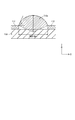
- FIG. 8 is a diagram schematically showing a cross section of the ink layer 116 a formed in the groove region between the banks 112.
- d indicates the opening width of the groove region
- ⁇ indicates the angle formed with respect to the horizontal plane at the location where the surface of the ink layer 116 a contacts the bank 112.
- the surface area of the ink layer 116a is expressed by (Ld ⁇ / sin ⁇ ).
- the area of the groove region in which the ink layer 116a is formed is represented by dL.
- the surface area of the ink layer 116a per groove area unit area is represented by ( ⁇ / sin ⁇ ).
- the volume of the ink layer 116a is substantially equal to the volume of the sectional sector area hatched with diagonal lines in the drawing, it is (Ld 2 ⁇ / 4sin 2 ⁇ ).
- the opening width d of the groove region is constant, when the volume of the ink layer 116a in the groove region is increased, the angle ⁇ made with respect to the horizontal plane at the portion where the surface of the ink layer 116a is in contact with the bank 112 increases, and the ink The surface area of the layer 116a also increases. Therefore, when the opening width d of the groove region is constant, the volume of the ink layer 116a may be increased in order to increase the surface area of the ink layer 116a.
- the surface area of the ink layer 116a per groove area unit area, the evaporation amount per groove area unit area, and the vapor density above the surface area are considered to be approximately proportional. Therefore, in order to make the evaporation rate of the groove region uniform, the surface area of the ink layer 116a per groove region unit area may be made uniform by increasing the volume of the ink layer 116a per groove region unit area.
- the ink layer 116 may be unevenly distributed due to different timings at which drying is completed in the ink layer 116a between the groove regions 125R, 125G, and 125B.
- the ink layer 116a in the groove region 125G is dried to form the hole transport layer 116G. Then, since the solvent evaporates from the groove region 125R and the solvent does not evaporate from the groove regions 125G and 125B, the distribution of the solvent vapor pressure above the banked substrate 150 is low on the groove regions 125G and 125B. Become. At locations close to the groove region 125B and the groove region 125G, the speed at which the solvent evaporates from the ink layer 116a on the groove region 125R increases (see the arrow in FIG. 7C). In each ink layer 116a, an ink flow occurs as indicated by white arrows in FIG.
- the ink layer 116a in the groove region 125R is dried to form the hole transport layer 116R.
- the solvent vapor pressure distribution is generated on the substrate during the drying, and the ink flow is generated in the ink layer 116 a, thereby forming each groove region 125.
- the thickness distribution of the hole transport layer 116 is biased as shown in FIG.
- the ink layer 116a formed in the groove regions 125R, 125G, and 125B is provided with a step of applying a solvent. ),
- the ink amount per unit area is uniform, and the surface area of the ink layer per groove area unit area is also uniform.
- the vapor pressure is equal on any of the groove regions 125R, 125G, and 125B, and the time when the drying is finished is also close. Therefore, the thickness distribution of the hole transport layer 116 formed in each groove region 125 is not biased.
- the film thickness of the hole transport layer 116 can be uniformly formed in each groove region 125, a resonator structure matching the wavelength of the emission color can be formed in each light emitting element 11 as a whole.
- the current density is made uniform by making the film thickness of the functional layer (hole transport layer 116) uniform in the light emitting element 11, an effect of extending the life of the light emitting element can be obtained.
- the three grooves The amount of ink applied to the regions 125R, 125G, and 125B must be different, but by applying the solvent as described above, the thickness distribution of the hole transport layer 116 in the light emitting element 11 can be made uniform. High utility value.
- the solvent is applied before applying ink to each of the groove regions 125R, 125G, and 125B.
- the order is changed and the solvent is applied after applying ink to each of the groove regions 125R, 125G, and 125B. May be.
- an effect of eliminating the uneven thickness of the hole transport layer 116 in each of the groove regions 125R, 125G, and 125B can be obtained.
- the ink may dry before the solvent is applied.
- the solvent is applied before the ink, In this case, the ink and the solvent applied to each groove region are mixed well.
- the light emitting layer 117 is formed by applying the ink for forming the light emitting layer to the groove regions 125R, 125G, and 125B in which the hole transport layer 116 is formed in the banked substrate 150 and drying it.
- the ink for forming the light emitting layer is a solution in which the material of the light emitting layer 117 is dissolved in a solvent.
- This ink application is also performed by ejecting the light emitting layer ink from the nozzle head to each of the groove regions 125R, 125G, and 125B while scanning the nozzle head along the surface of the banked substrate 150.
- the red light emitting layer ink is applied to the groove region 125R
- the green light emitting layer ink is applied to the groove region 125G
- the blue light emitting layer ink is applied to the groove region 125B.
- the ink is applied as in the step of forming the hole transport layer 116.
- the surface area of the ink layer per unit area of the groove region can be reduced by applying a solvent before or after the application, and uniformizing the total amount of ink and solvent per unit area between the groove regions 125R, 125G, and 125B.
- the effect of making uniform and making the film thickness distribution of the light emitting layer 117 uniform in each of the groove regions 125R, 125G, and 125B can be obtained.
- FIGS. 9 and 10 are diagrams showing the configuration of the display panel 20 according to the second embodiment.
- This display panel 20 has the same basic configuration as that of the display panel 10 according to the first embodiment, except that a bus bar region 126 is secured between adjacent groove region groups 12 on the substrate 110. The difference is that a bus bar 105 extending in the Y direction is provided.
- the bus bar 105 is formed in the same layer as the pixel electrode 103 on the upper surface of the interlayer insulating layer 102.
- the upper surface side of the bus bar 105 is in continuous contact with the cathode 119 in the Y direction via the hole injection layer 104 and is electrically connected.
- the cathode 119 is electrically connected to the bus bar 105 along the Y direction, the electrical resistance in the Y direction is reduced.
- the method of manufacturing the display panel 20 is the same as the method of manufacturing the display panel 10 of the first embodiment, but in the process of forming the pixel electrode 103, the bus bar 105 is also formed at the same time.
- FIGS. 11A to 11E are schematic cross-sectional views showing a process of forming a hole transport layer in the groove regions 125R, 125G, and 125B.
- the application per unit area of the hole transport layer ink applied to each of the groove regions 125R, 125G, and 125B is also set to be smaller in this order, and only the solvent is applied to the groove regions 125G and 125B prior to ink application. Further, as shown in FIGS. 11A and 11B, the application amount of the solvent per unit area to the groove regions 125R, 125G, and 125B is set so as to increase in this order. This is the same as the first embodiment.
- bus bar region 126 is provided between the adjacent groove region groups 12, when the solvent is applied to the groove regions 125G and 125B, FIGS. The solvent is also applied to the bus bar region 126 as shown in FIG.
- the amount of the solvent applied to the bus bar region 126 is such that the surface of the solvent layer applied is the bank 112 so that the surface area of the solvent layer per unit area of the bus bar region is equal to the surface area of the ink layer 116a per unit area of the groove region. It is preferable that the angle formed with the horizontal plane at the position where the ink layer 116a contacts with the bank 112 and the angle formed with the horizontal plane at the position where the surface of the ink layer 116a contacts the bank 112 (angle ⁇ in FIG. 8) are preferably set.
- the ink layer 116a is formed in the groove regions 125R, 125G, and 125B, and the solvent layer is formed in the bus bar region 126. Therefore, the following effects are achieved.
- the solvent vapor pressure above the banked substrate 150 is lowered above the bus bar region 126.
- the speed at which the solvent evaporates from the ink layer 116a on the groove region 125G and the ink layer 116a on the groove region 125R increases, and an ink flow is generated.
- the film thickness distribution becomes non-uniform.
- the ink layer 116a in the groove regions 125R, 125G, and 125B is dried in a state where the solvent exists in the bus bar region 126, the distribution of the solvent vapor pressure above the banked substrate 150 is as follows.
- the ink layer 116a is dried in a uniform state.
- FIG. 12A and 12B are plan views of the display panel 30 according to the third embodiment.
- the width of the light emitting element 11B is set wider than that of the light emitting elements 11R and 11G. That is, the opening width of the blue groove region 125B is set wider than that of the red groove region 125R and the green groove region 125G.
- blue light-emitting elements are more likely to deteriorate during driving than red light-emitting elements and green light-emitting elements.
- the width of the blue light-emitting element 11B in this way, the current density is secured while ensuring the amount of light emission. Can reduce the deterioration rate.
- the application amount per unit area of the ink for the hole transport layer applied to the groove regions 125R, 125G, and 125B is set so as to decrease in this order. Prior to ink application, only the solvent is applied to the groove regions 125R, 125G, and 125B (however, the solvent may not be applied to the groove region 125R). The application amount of the solvent per unit area for each groove region 125R, 125G, 125B is set to increase in this order.
- the volume and surface area of the ink layer 116a per groove area unit area between the groove areas 125R, 125G, and 125B are made uniform by setting the coating amount per unit area of the solvent for the groove areas 125R, 125G, and 125B.
- the distribution of the solvent vapor pressure on the substrate 110 is made uniform, and the ink flow is less likely to occur in each groove region.
- the film thickness distribution of the hole transport layer 116 formed in the groove regions 125R, 125G, and 125B becomes uniform.
- the amount of solvent applied to each groove region 125R, 125G, and 125B may be set so that the surface area per groove region unit area is equal. preferable.
- the opening width of the groove region 125B is wider than the opening width of the groove regions 125R and 125G.
- ratio S / V 4 sin ⁇ / d
- the groove region 125B has a larger ink layer 116a per groove region unit area than the groove regions 125R and 125G. What is necessary is just to set solvent application amount so that the volume V may become large.
- the display panel 30 shown in FIG. 12B is an example having a pixel bank.
- a plurality of banks 112 extending in the Y direction and a plurality of banks 113 extending in the X direction intersect to form a pixel bank. Then, regions surrounded by the banks 112 and 113 become groove regions 125R, 125G, and 125B, and the light emitting elements 11R, 11G, and 11B are formed.
- the method described in the first embodiment is also used in the step of forming the hole transport layer 116.
- the functional layer is formed in the groove region partitioned by the pixel bank as in the case of producing the display panel 30 shown in FIG. 12B, the same effect can be obtained.
- one groove region group 12 is composed of three groove regions 125R, 125G, and 125B, and the ink application amount per unit area is different between the three groove regions 125R, 125G, and 125B.
- the solvent application amount per unit area is different from each other, but two of the three groove regions 125R, 125G, and 125B have the same ink application amount and only one ink application amount. Even if they are different, it can be similarly implemented.
- the ink application amount per unit area is different between the three groove regions 125R, 125G, and 125B, two of the three groove regions 125R, 125G, and 125B have the same solvent application amount and 1 There may be cases where the solvent application amount is different. In that case, in the three groove regions 125R, 125G, and 125B, even if the surface area of the ink layer per groove region unit area does not become equal, an effect of uniformization can be obtained to some extent, so that each groove region 125R, 125G, The effect of eliminating the uneven thickness of the hole transport layer 116 formed in 125B can be obtained.
- one pixel is composed of three light emitting elements 11R, 11G, and 11B
- one groove region group 12 is composed of three groove regions 125R, 125G, and 125B. Even when the groove region group is composed of two groove regions, the present invention can be similarly implemented, and the film thickness distribution of the hole transport layer formed in each groove region becomes uniform.
- one pixel is composed of four or more light emitting elements 11R, 11G, and 11B, and one groove region group 12 is composed of four or more groove regions, it can be similarly implemented. Similar effects can be obtained.
- the present invention is not limited to the organic EL display panel, and can be applied to, for example, forming a functional layer in organic EL lighting, and the same effect can be obtained.
- the plurality of groove region groups 12 existing on the base substrate it is located in the peripheral portion rather than the average of the coating amount per unit area of the solvent in the groove region group 12 located in the central portion of the base substrate.
- the average coating amount per unit area of the solvent in the groove region group to be set may be set large.
- the solvent evaporation rate tends to increase in the peripheral groove region group 12 as compared to the central groove region group 12 of the base substrate, the unit area of the solvent in the groove region group 12 positioned in the peripheral portion as described above.
- the average coating amount per unit larger than the average amount per unit area of the solvent in the groove region group located in the center, drying of the ink layer is completed between the center and the periphery. You can adjust the time to do. Adding such a setting also contributes to uniforming the film thickness distribution of the functional layers 116R, 116G, and 116B formed in the groove regions 125R, 125G, and 125B.
- the method for forming a functional layer according to the present invention is useful for manufacturing an organic light emitting device such as an organic EL display device.
Landscapes
- Engineering & Computer Science (AREA)
- Manufacturing & Machinery (AREA)
- Physics & Mathematics (AREA)
- Optics & Photonics (AREA)
- Microelectronics & Electronic Packaging (AREA)
- Electroluminescent Light Sources (AREA)
Abstract
Description
本発明者は、下地基板の表面に沿った複数のバンクによって区画された複数の各溝領域にサブピクセルが形成された有機発光デバイスの製造について検討した。この検討の結果、本発明者は、当該有機発光デバイスの製造の際に、各溝領域にインクの塗布を行うことによって機能層を形成するときに、溝領域ごとにインクの塗布量が異なっていると、各溝領域に形成される機能層の膜厚分布に偏りが生じることを見出した。
本発明の一態様に係る有機発光デバイスの機能層を形成する方法は、下地基板と、当該下地基板の表面に沿った一方向に伸長し互いに並行する複数のバンクとを有するバンク付基板を準備し、複数のバンク同士の間の各溝領域にインクを塗布し、塗布されたインク層を乾燥させることによって、色の異なる隣り合う複数のサブピクセルからなる画素が複数配置された有機発光デバイスの機能層を形成する形成方法であって、バンク付基板において、それぞれ色の異なるサブピクセルが形成される隣り合う複数の溝領域からなる溝領域群が複数群存在し、各溝領域群において、一部の溝領域は、残りの溝領域と比べて、単位面積当たりのインク塗布量が少なく設定され、複数の溝領域の各々にインクを塗布する前又は後に、一部の溝領域にインクが溶解する溶剤を塗布すると共に、残りの溝領域に対しては、インクが溶解する溶剤を塗布しないか、一部の溝領域に対する単位面積当たりの塗布量より少ない単位面積当たりの塗布量で溶剤を塗布し、インク及び溶剤の塗布によって複数の溝領域に形成されたインク層を乾燥させることによって機能層を形成することとした。
以下、実施の形態に係る有機EL装置の構成及び製法について説明する。
図1および図2を参照しながら、有機EL表示装置1の概略構成を説明する。
表示パネル10において、Y方向に延伸する複数のバンク112によって区画された溝領域125R,125G,125Bが形成されている。溝領域125R,125G,125Bは、赤色用、緑色用、青色用の溝領域であって、対応する発光色の発光素子11R,11G,11BがY方向に列設されている。
基板100:
基板100は、例えば、ガラス基板、石英基板、シリコン基板、硫化モリブデン、銅、亜鉛、アルミニウム、ステンレス、マグネシウム、鉄、ニッケル、金、銀などの金属基板、ガリウム砒素基などの半導体基板、プラスチック基板等を用い形成されている。
表示パネル10の製造工程において、エッチング処理、ベーク処理等が施されることがあるので、層間絶縁層102は、それらの処理に対して耐久性を有する材料で形成することが望ましい。層間絶縁層102は、例えば、ポリイミド、ポリアミド、アクリル系樹脂などの有機化合物で形成される。
表示パネル10はトップエミッション型なので、画素電極103の表面は高い反射性を有することが好ましい。画素電極103は、例えば、銀(Ag)またはアルミニウム(Al)を含む金属材料で構成される。
ホール注入層104は、例えば、銀(Ag)、モリブデン(Mo)、クロム(Cr)、バナジウム(V)、タングステン(W)、ニッケル(Ni)、イリジウム(Ir)などの酸化物、あるいは、PEDOT(ポリチオフェンとポリスチレンスルホン酸との混合物)などの導電性ポリマー材料からなる。
バンク112は、感光性の有機材料で形成する。有機材料の具体例として、例えば、アクリル系樹脂、ポリイミド系樹脂、シロキサン系樹脂、フェノール系樹脂などが挙げられる。
ホール輸送層116は、例えば、ポリフルオレンやその誘導体、あるいはポリアリールアミンやその誘導体などの高分子化合物を用いて形成することができる。
発光層117の材料としては、パラフェニレンビニレン(PPV)、ポリフルオレン、オキシノイド化合物、ペリレン化合物、クマリン化合物、アザクマリン化合物、オキサゾール化合物、オキサジアゾール化合物、ペリノン化合物、ピロロピロール化合物、ナフタレン化合物、アントラセン化合物、フルオレン化合物、フルオランテン化合物、テトラセン化合物、ピレン化合物、コロネン化合物、キノロン化合物及びアザキノロン化合物、ピラゾリン誘導体及びピラゾロン誘導体、ローダミン化合物、クリセン化合物、フェナントレン化合物、シクロペンタジエン化合物、スチルベン化合物、ジフェニルキノン化合物、スチリル化合物、ブタジエン化合物、ジシアノメチレンピラン化合物、ジシアノメチレンチオピラン化合物、フルオレセイン化合物、ピリリウム化合物、チアピリリウム化合物、セレナピリリウム化合物、テルロピリリウム化合物、芳香族アルダジエン化合物、オリゴフェニレン化合物、チオキサンテン化合物、シアニン化合物、アクリジン化合物、8-ヒドロキシキノリン化合物の金属錯体、2-ビピリジン化合物の金属錯体、シッフ塩とIII族金属との錯体、オキシン金属錯体、希土類錯体等の蛍光物質等が挙げられる。
電子輸送層118は、例えば、オキサジアゾール誘導体(OXD)、トリアゾール誘導体(TAZ)、フェナンスロリン誘導体(BCP、Bphen)などで形成される。
表示パネル10はトップエミッション型なので、カソード119は光透過性の材料で形成する。具体的な材料は、例えば、酸化インジウムスズ(ITO)若しくは酸化インジウム亜鉛(IZO)などである。
封止層120は、光透過性の材料で形成される。
樹脂層121は、透明樹脂材料、例えば、エポキシ系樹脂材料から形成される。ただし、これ以外にもシリコーン系樹脂などを用いることもできる。
ブラックマトリクス層122は、光吸収性および遮光性に優れる黒色顔料を含む紫外線硬化樹脂材料で形成されている。紫外線硬化樹脂としては、アクリル系の紫外線硬化樹脂材料が挙げられる。
カラーフィルタ層123は、赤色(R)、緑色(G)、青色(B)の各色の波長域の可視光を選択的に透過する材料、例えば公知のアクリル樹脂をベースにした材料で形成される。
基板124は、上記基板100と同様に、例えば、ガラス基板、石英基板、シリコン基板、硫化モリブデン、銅、亜鉛、アルミニウム、ステンレス、マグネシウム、鉄、ニッケル、金、銀などの金属基板、ガリウム砒素基などの半導体基板、プラスチック基板等を用いることができる。
表示パネル10の製造方法について、図4の工程図に基づいて説明する。
図6(a)~(e)は、溝領域125R,125G,125Bにホール輸送層を形成する工程を示す断面模式図である。
上記ホール輸送層116の形成工程によれば、各溝領域群12を構成する3つの溝領域125R,125G,125Bにおいて、単位面積あたりのインク塗布量が多い溝領域125Rは、残りの溝領域125G、125Bと比べて単位面積あたりの溶剤塗布量が小さく設定されている。
上記ホール輸送層116の形成工程の説明では、まずノズルヘッド221を走査しながら各溝領域125R,125G,125Bに溶剤を塗付した後、ノズルヘッド222を走査しながら各溝領域125R,125G,125Bにインクを塗付したが、ノズルヘッド221及びノズルヘッド222を走査しながら、一回の走査で、各溝領域125R,125G,125Bに溶剤の塗布とインク塗布とを行うこともできる。この場合も同様に、各溝領域125R,125G,125B内でホール輸送層116の膜厚の偏りをなくす効果が得られる。
バンク付基板150におけるホール輸送層116が形成された各溝領域125R,125G,125Bに対して、発光層形成用のインクを塗布し乾燥することによって発光層117を形成する。
図9,図10は、実施の形態2に係る表示パネル20の構成を示す図である。
図12(a),(b)は、実施の形態3に係る表示パネル30の平面図である。
(1)上記実施の形態では、1つの溝領域群12が3つの溝領域125R,125G、125Bで構成され、単位面積当たりのインク塗布量が3つの溝領域125R,125G、125Bで相互に異なっていて、且つ単位面積当たりの溶剤塗布量も相互に異なっている例を示したが、3つの溝領域125R,125G、125Bの中の2つはインク塗布量が同じで1つだけインク塗布量が異なっている場合でも、同様に実施できる。
10 表示パネル
11R 赤色発光素子
11G 緑色発光素子
11B 青色発光素子
12 溝領域群
20 表示パネル
30 表示パネル
100 基板
101 TFT層
102 層間絶縁層
103 画素電極
104 ホール注入層
105 バスバー
110 下地基板
112 バンク
113 バンク
116 ホール輸送層
116a インク層
117 発光層
118 電子輸送層
119 カソード
120 封止層
121 樹脂層
124 基板
125R,125G,125B 溝領域
126 バスバー領域
150 バンク付基板
Claims (8)
- 下地基板と、当該下地基板の表面に沿った一方向に伸長し互いに並行する複数のバンクとを有するバンク付基板を準備し、前記複数のバンクのうち隣り合うバンク同士の間の各溝領域にインクを塗布し、塗布されたインク層を乾燥させることによって、色の異なる隣り合う複数のサブピクセルからなる画素が複数配置された有機発光デバイスの機能層を形成する形成方法であって、
前記バンク付基板において、それぞれ色の異なるサブピクセルが形成される隣り合う複数の溝領域からなる溝領域群が複数群存在し、
各溝領域群において、一部の溝領域は、残りの溝領域と比べて、単位面積当たりのインク塗布量が少なく設定され、
前記複数の溝領域の各々にインクを塗布する前又は後に、
前記一部の溝領域に前記インクが溶解する溶剤を塗布すると共に、
前記残りの溝領域に対しては、前記インクが溶解する溶剤を塗布しないか、前記一部の溝領域に対する単位面積当たりの塗布量より少ない単位面積当たりの塗布量で前記溶剤を塗布し、
前記インク及び前記溶剤の塗布によって前記複数の溝領域の各々に形成されたインク層を乾燥させることによって前記機能層を形成する、
機能層の形成方法。 - 前記複数の溝領域の各々に塗布される前記溶剤の塗布量は、
各溝領域の単位面積あたりに形成されるインク層の表面積が同等となるように設定されている、
請求項1記載の機能層の形成方法。 - 前記下地基板上における前記複数の溝領域群のうち隣り合う溝領域群同士の間に、バスバーが配置された間隙が存在し、
前記溶剤を塗布するときに、前記バスバーが配置された間隙にも前記溶剤を塗布する、
請求項1又は2に記載の機能層の形成方法。 - 前記複数の溝領域群の中で、前記下地基板の中央部に位置する溝領域群における前記溶剤の単位面積当たりの塗布量の平均よりも、前記下地基板の周辺部に位置する溝領域群における前記溶剤の単位面積当たりの塗布量の平均が大きく設定されている、
請求項1~3のいずれかに記載の機能層の形成方法。 - 前記複数の溝領域の各々に対して前記インクを塗布する前に、前記溶剤の塗布を行う、
請求項1~4のいずれかに記載の機能層の形成方法。 - 前記溶剤には、前記インクに含まれる溶剤と共通の成分が含まれる、
請求項1~5のいずれかに記載の機能層の形成方法。 - 前記下地基板上に前記機能層を形成することによって有機発光デバイスを製造する方法であって、
前記機能層を形成する際に、請求項1~6のいずれかに記載の機能層の形成方法を用いる、
有機発光デバイスの製造方法。 - 下地基板と当該下地基板の表面に沿った一方向に伸長し互いに並行する複数のバンクとを有し、前記複数のバンクのうち隣り合うバンク同士の間には各溝領域が存在し、且つ、それぞれ色の異なるサブピクセルが形成される隣り合う複数の溝領域からなる溝領域群が複数群存在するバンク付基板を備えた有機発光デバイスを製造する装置であって、
インクで構成される第1液滴を吐出する第1インクジェットヘッドと、
前記インクが溶解する溶剤で構成される第2液滴を吐出する第2インクジェットヘッドと、
各溝領域群における一部の溝領域に対して、残りの溝領域と比べて、単位面積当たりのインク塗布量が少なくなるよう、前記第1インクジェットヘッドに前記第1液滴を吐出させるとともに、前記一部の溝領域に対して、前記第2インクジェットヘッドに前記第2液滴を吐出させ、前記残りの溝領域に対して、前記第2インクジェットヘッドに前記第2液滴を吐出させないか、前記一部の溝領域に対する単位面積当たりの塗布量より少ない単位面積当たりの塗布量で前記第2インクジェットヘッドに前記第2液滴を吐出させる制御部と、
を備える有機発光デバイスの製造装置。
Priority Applications (2)
| Application Number | Priority Date | Filing Date | Title |
|---|---|---|---|
| US15/306,610 US9640592B2 (en) | 2014-04-30 | 2015-04-22 | Method for forming functional layer of organic light-emitting device and method for manufacturing organic light-emitting device |
| JP2016515857A JP6232660B2 (ja) | 2014-04-30 | 2015-04-22 | 有機発光デバイスの機能層の形成方法及び有機発光デバイスの製造方法 |
Applications Claiming Priority (2)
| Application Number | Priority Date | Filing Date | Title |
|---|---|---|---|
| JP2014-093447 | 2014-04-30 | ||
| JP2014093447 | 2014-04-30 |
Publications (1)
| Publication Number | Publication Date |
|---|---|
| WO2015166647A1 true WO2015166647A1 (ja) | 2015-11-05 |
Family
ID=54358392
Family Applications (1)
| Application Number | Title | Priority Date | Filing Date |
|---|---|---|---|
| PCT/JP2015/002178 Ceased WO2015166647A1 (ja) | 2014-04-30 | 2015-04-22 | 有機発光デバイスの機能層の形成方法及び有機発光デバイスの製造方法 |
Country Status (3)
| Country | Link |
|---|---|
| US (1) | US9640592B2 (ja) |
| JP (1) | JP6232660B2 (ja) |
| WO (1) | WO2015166647A1 (ja) |
Cited By (2)
| Publication number | Priority date | Publication date | Assignee | Title |
|---|---|---|---|---|
| JP2021516841A (ja) * | 2018-03-28 | 2021-07-08 | 京東方科技集團股▲ふん▼有限公司Boe Technology Group Co.,Ltd. | 有機発光表示パネルおよびその作製方法、表示装置 |
| KR20250018080A (ko) | 2023-07-28 | 2025-02-04 | 캐논 가부시끼가이샤 | 유기 el 디바이스의 제조 방법, 및 도포 장치 |
Families Citing this family (4)
| Publication number | Priority date | Publication date | Assignee | Title |
|---|---|---|---|---|
| JP6685675B2 (ja) | 2015-09-07 | 2020-04-22 | 株式会社Joled | 有機el素子、それを用いた有機el表示パネル、及び有機el表示パネルの製造方法 |
| JP6964421B2 (ja) | 2017-03-23 | 2021-11-10 | ローム株式会社 | 半導体発光装置 |
| CN107799575B (zh) * | 2017-10-31 | 2020-04-24 | 京东方科技集团股份有限公司 | 显示器基板、其制造方法、显示器及补偿构件贴片 |
| KR20240045247A (ko) * | 2021-08-02 | 2024-04-05 | 메르크 파텐트 게엠베하 | 잉크들을 결합하는 것에 의한 프린팅 방법 |
Citations (10)
| Publication number | Priority date | Publication date | Assignee | Title |
|---|---|---|---|---|
| JP2001291583A (ja) * | 2000-04-07 | 2001-10-19 | Seiko Epson Corp | 有機el素子および有機el素子の製造方法 |
| JP2004031070A (ja) * | 2002-06-25 | 2004-01-29 | Toshiba Corp | 有機el材料塗布装置とその塗布方法および有機el表示装置 |
| JP2006202587A (ja) * | 2005-01-20 | 2006-08-03 | Seiko Epson Corp | 電気光学装置の製造方法、電気光学装置及び電子機器 |
| JP2006212589A (ja) * | 2005-02-07 | 2006-08-17 | Seiko Epson Corp | 組成物の製造方法、電気光学装置の製造方法、および液滴吐出装置 |
| JP2008186766A (ja) * | 2007-01-31 | 2008-08-14 | Toppan Printing Co Ltd | 有機エレクトロルミネッセンス素子の製造方法 |
| JP2008270182A (ja) * | 2007-03-22 | 2008-11-06 | Semiconductor Energy Lab Co Ltd | 発光装置の作製方法 |
| JP2009247933A (ja) * | 2008-04-02 | 2009-10-29 | Seiko Epson Corp | 液状体吐出方法、有機elパネルの製造方法、カラーフィルタの製造方法、表示装置、および電子機器 |
| JP2010161070A (ja) * | 2008-12-10 | 2010-07-22 | Panasonic Corp | 光学素子および光学素子を具備する表示装置の製造方法 |
| JP2013118095A (ja) * | 2011-12-02 | 2013-06-13 | Dainippon Printing Co Ltd | 有機エレクトロルミネッセンス素子の製造方法 |
| JP2013214396A (ja) * | 2012-04-02 | 2013-10-17 | Seiko Epson Corp | 機能膜の形成方法、有機elパネルの製造方法、表示装置 |
Family Cites Families (6)
| Publication number | Priority date | Publication date | Assignee | Title |
|---|---|---|---|---|
| JP4894150B2 (ja) | 2005-03-15 | 2012-03-14 | セイコーエプソン株式会社 | 電気光学装置の製造方法、液滴吐出装置 |
| JP2007234232A (ja) | 2006-02-27 | 2007-09-13 | Hitachi Displays Ltd | 画像表示装置 |
| US7888867B2 (en) * | 2007-12-28 | 2011-02-15 | Panasonic Corporation | Organic el device having bank with groove, organic el display panel, and method for manufacturing the organic el device |
| KR101254748B1 (ko) * | 2009-05-06 | 2013-04-15 | 엘지디스플레이 주식회사 | 유기전계발광표시장치 및 이의 제조방법 |
| CN102449767A (zh) | 2010-08-06 | 2012-05-09 | 松下电器产业株式会社 | 有机el显示面板、显示装置以及有机el显示面板的制造方法 |
| KR20130044117A (ko) | 2010-08-06 | 2013-05-02 | 파나소닉 주식회사 | 유기 el 표시 패널, 표시 장치, 및 유기 el 표시 패널의 제조 방법 |
-
2015
- 2015-04-22 US US15/306,610 patent/US9640592B2/en active Active
- 2015-04-22 JP JP2016515857A patent/JP6232660B2/ja active Active
- 2015-04-22 WO PCT/JP2015/002178 patent/WO2015166647A1/ja not_active Ceased
Patent Citations (10)
| Publication number | Priority date | Publication date | Assignee | Title |
|---|---|---|---|---|
| JP2001291583A (ja) * | 2000-04-07 | 2001-10-19 | Seiko Epson Corp | 有機el素子および有機el素子の製造方法 |
| JP2004031070A (ja) * | 2002-06-25 | 2004-01-29 | Toshiba Corp | 有機el材料塗布装置とその塗布方法および有機el表示装置 |
| JP2006202587A (ja) * | 2005-01-20 | 2006-08-03 | Seiko Epson Corp | 電気光学装置の製造方法、電気光学装置及び電子機器 |
| JP2006212589A (ja) * | 2005-02-07 | 2006-08-17 | Seiko Epson Corp | 組成物の製造方法、電気光学装置の製造方法、および液滴吐出装置 |
| JP2008186766A (ja) * | 2007-01-31 | 2008-08-14 | Toppan Printing Co Ltd | 有機エレクトロルミネッセンス素子の製造方法 |
| JP2008270182A (ja) * | 2007-03-22 | 2008-11-06 | Semiconductor Energy Lab Co Ltd | 発光装置の作製方法 |
| JP2009247933A (ja) * | 2008-04-02 | 2009-10-29 | Seiko Epson Corp | 液状体吐出方法、有機elパネルの製造方法、カラーフィルタの製造方法、表示装置、および電子機器 |
| JP2010161070A (ja) * | 2008-12-10 | 2010-07-22 | Panasonic Corp | 光学素子および光学素子を具備する表示装置の製造方法 |
| JP2013118095A (ja) * | 2011-12-02 | 2013-06-13 | Dainippon Printing Co Ltd | 有機エレクトロルミネッセンス素子の製造方法 |
| JP2013214396A (ja) * | 2012-04-02 | 2013-10-17 | Seiko Epson Corp | 機能膜の形成方法、有機elパネルの製造方法、表示装置 |
Cited By (3)
| Publication number | Priority date | Publication date | Assignee | Title |
|---|---|---|---|---|
| JP2021516841A (ja) * | 2018-03-28 | 2021-07-08 | 京東方科技集團股▲ふん▼有限公司Boe Technology Group Co.,Ltd. | 有機発光表示パネルおよびその作製方法、表示装置 |
| JP7510758B2 (ja) | 2018-03-28 | 2024-07-04 | 京東方科技集團股▲ふん▼有限公司 | 有機発光表示パネルおよびその作製方法、表示装置 |
| KR20250018080A (ko) | 2023-07-28 | 2025-02-04 | 캐논 가부시끼가이샤 | 유기 el 디바이스의 제조 방법, 및 도포 장치 |
Also Published As
| Publication number | Publication date |
|---|---|
| JP6232660B2 (ja) | 2017-11-22 |
| US20170047381A1 (en) | 2017-02-16 |
| JPWO2015166647A1 (ja) | 2017-04-20 |
| US9640592B2 (en) | 2017-05-02 |
Similar Documents
| Publication | Publication Date | Title |
|---|---|---|
| JP6594859B2 (ja) | 有機発光デバイスおよびその製造方法 | |
| US10720478B2 (en) | Organic EL display panel, organic EL display device, and organic EL display panel manufacturing method | |
| US10714549B2 (en) | Organic EL display panel manufacturing method and organic EL display panel | |
| JP6594863B2 (ja) | 有機el表示パネル及び有機el表示装置 | |
| US11038133B2 (en) | Organic EL display panel, organic EL display device, and manufacturing method of organic display panel | |
| JP6612446B2 (ja) | 有機el表示パネル及びその製造方法 | |
| JP6232660B2 (ja) | 有機発光デバイスの機能層の形成方法及び有機発光デバイスの製造方法 | |
| JP2019207836A (ja) | 有機el表示パネル、有機el表示装置、及び、有機el表示パネルの製造方法 | |
| JP2020030933A (ja) | 有機el表示パネル、及び有機el表示パネルの製造方法 | |
| JP2016091841A (ja) | 有機発光デバイスと有機表示装置 | |
| JPWO2017204150A1 (ja) | 有機el表示パネル、有機el表示装置、及び、その製造方法 | |
| JP2019125501A (ja) | 有機el表示パネル及びその製造方法 | |
| JP6861495B2 (ja) | 有機el素子及びその製造方法 | |
| JP2019021569A (ja) | 有機el表示パネル、有機el表示装置、および、製造方法 | |
| JP2018060677A6 (ja) | 有機el素子及びその製造方法 | |
| JP2015207526A (ja) | 有機発光デバイスの機能層の形成方法 | |
| JP5899531B2 (ja) | 有機el素子の製造方法 | |
| JP2015207527A (ja) | 有機発光デバイスの機能層の形成方法及び有機発光デバイスの製造方法 | |
| JP6019372B2 (ja) | 発光素子及び発光パネル | |
| JP7412999B2 (ja) | 有機el表示パネル、及び有機el表示パネルの製造方法 | |
| JP2019133835A (ja) | 有機el表示パネル及び有機el表示パネルの製造方法 | |
| JP2020009676A (ja) | 有機el表示パネル及び有機el表示パネルの製造方法 | |
| CN110783494B (zh) | 有机el显示面板的制造方法 | |
| JP2019021385A (ja) | 有機el表示パネル、および、有機el表示装置 | |
| JP2016015292A (ja) | 有機el表示装置 |
Legal Events
| Date | Code | Title | Description |
|---|---|---|---|
| 121 | Ep: the epo has been informed by wipo that ep was designated in this application |
Ref document number: 15785537 Country of ref document: EP Kind code of ref document: A1 |
|
| ENP | Entry into the national phase |
Ref document number: 2016515857 Country of ref document: JP Kind code of ref document: A |
|
| WWE | Wipo information: entry into national phase |
Ref document number: 15306610 Country of ref document: US |
|
| NENP | Non-entry into the national phase |
Ref country code: DE |
|
| 122 | Ep: pct application non-entry in european phase |
Ref document number: 15785537 Country of ref document: EP Kind code of ref document: A1 |