WO2015163074A1 - 光学センサシステム、光学式ガスセンサシステム、微粒子センサシステム、発光装置、および画像印刷装置 - Google Patents
光学センサシステム、光学式ガスセンサシステム、微粒子センサシステム、発光装置、および画像印刷装置 Download PDFInfo
- Publication number
- WO2015163074A1 WO2015163074A1 PCT/JP2015/058921 JP2015058921W WO2015163074A1 WO 2015163074 A1 WO2015163074 A1 WO 2015163074A1 JP 2015058921 W JP2015058921 W JP 2015058921W WO 2015163074 A1 WO2015163074 A1 WO 2015163074A1
- Authority
- WO
- WIPO (PCT)
- Prior art keywords
- light
- sensor system
- light emission
- optical sensor
- environmental parameter
- Prior art date
- Legal status (The legal status is an assumption and is not a legal conclusion. Google has not performed a legal analysis and makes no representation as to the accuracy of the status listed.)
- Ceased
Links
Images



Classifications
-
- G—PHYSICS
- G01—MEASURING; TESTING
- G01N—INVESTIGATING OR ANALYSING MATERIALS BY DETERMINING THEIR CHEMICAL OR PHYSICAL PROPERTIES
- G01N21/00—Investigating or analysing materials by the use of optical means, i.e. using sub-millimetre waves, infrared, visible or ultraviolet light
- G01N21/17—Systems in which incident light is modified in accordance with the properties of the material investigated
- G01N21/47—Scattering, i.e. diffuse reflection
- G01N21/49—Scattering, i.e. diffuse reflection within a body or fluid
- G01N21/53—Scattering, i.e. diffuse reflection within a body or fluid within a flowing fluid, e.g. smoke
-
- G—PHYSICS
- G01—MEASURING; TESTING
- G01N—INVESTIGATING OR ANALYSING MATERIALS BY DETERMINING THEIR CHEMICAL OR PHYSICAL PROPERTIES
- G01N21/00—Investigating or analysing materials by the use of optical means, i.e. using sub-millimetre waves, infrared, visible or ultraviolet light
- G01N21/17—Systems in which incident light is modified in accordance with the properties of the material investigated
- G01N21/59—Transmissivity
- G01N21/61—Non-dispersive gas analysers
-
- G—PHYSICS
- G01—MEASURING; TESTING
- G01N—INVESTIGATING OR ANALYSING MATERIALS BY DETERMINING THEIR CHEMICAL OR PHYSICAL PROPERTIES
- G01N21/00—Investigating or analysing materials by the use of optical means, i.e. using sub-millimetre waves, infrared, visible or ultraviolet light
- G01N21/75—Systems in which material is subjected to a chemical reaction, the progress or the result of the reaction being investigated
- G01N21/77—Systems in which material is subjected to a chemical reaction, the progress or the result of the reaction being investigated by observing the effect on a chemical indicator
-
- G—PHYSICS
- G03—PHOTOGRAPHY; CINEMATOGRAPHY; ANALOGOUS TECHNIQUES USING WAVES OTHER THAN OPTICAL WAVES; ELECTROGRAPHY; HOLOGRAPHY
- G03G—ELECTROGRAPHY; ELECTROPHOTOGRAPHY; MAGNETOGRAPHY
- G03G15/00—Apparatus for electrographic processes using a charge pattern
- G03G15/04—Apparatus for electrographic processes using a charge pattern for exposing, i.e. imagewise exposure by optically projecting the original image on a photoconductive recording material
- G03G15/043—Apparatus for electrographic processes using a charge pattern for exposing, i.e. imagewise exposure by optically projecting the original image on a photoconductive recording material with means for controlling illumination or exposure
-
- G—PHYSICS
- G03—PHOTOGRAPHY; CINEMATOGRAPHY; ANALOGOUS TECHNIQUES USING WAVES OTHER THAN OPTICAL WAVES; ELECTROGRAPHY; HOLOGRAPHY
- G03G—ELECTROGRAPHY; ELECTROPHOTOGRAPHY; MAGNETOGRAPHY
- G03G15/00—Apparatus for electrographic processes using a charge pattern
- G03G15/50—Machine control of apparatus for electrographic processes using a charge pattern, e.g. regulating differents parts of the machine, multimode copiers, microprocessor control
-
- G—PHYSICS
- G03—PHOTOGRAPHY; CINEMATOGRAPHY; ANALOGOUS TECHNIQUES USING WAVES OTHER THAN OPTICAL WAVES; ELECTROGRAPHY; HOLOGRAPHY
- G03G—ELECTROGRAPHY; ELECTROPHOTOGRAPHY; MAGNETOGRAPHY
- G03G15/00—Apparatus for electrographic processes using a charge pattern
- G03G15/55—Self-diagnostics; Malfunction or lifetime display
-
- G—PHYSICS
- G03—PHOTOGRAPHY; CINEMATOGRAPHY; ANALOGOUS TECHNIQUES USING WAVES OTHER THAN OPTICAL WAVES; ELECTROGRAPHY; HOLOGRAPHY
- G03G—ELECTROGRAPHY; ELECTROPHOTOGRAPHY; MAGNETOGRAPHY
- G03G21/00—Arrangements not provided for by groups G03G13/00 - G03G19/00, e.g. cleaning, elimination of residual charge
- G03G21/20—Humidity or temperature control also ozone evacuation; Internal apparatus environment control
-
- H—ELECTRICITY
- H01—ELECTRIC ELEMENTS
- H01S—DEVICES USING THE PROCESS OF LIGHT AMPLIFICATION BY STIMULATED EMISSION OF RADIATION [LASER] TO AMPLIFY OR GENERATE LIGHT; DEVICES USING STIMULATED EMISSION OF ELECTROMAGNETIC RADIATION IN WAVE RANGES OTHER THAN OPTICAL
- H01S5/00—Semiconductor lasers
- H01S5/0014—Measuring characteristics or properties thereof
-
- H—ELECTRICITY
- H01—ELECTRIC ELEMENTS
- H01S—DEVICES USING THE PROCESS OF LIGHT AMPLIFICATION BY STIMULATED EMISSION OF RADIATION [LASER] TO AMPLIFY OR GENERATE LIGHT; DEVICES USING STIMULATED EMISSION OF ELECTROMAGNETIC RADIATION IN WAVE RANGES OTHER THAN OPTICAL
- H01S5/00—Semiconductor lasers
- H01S5/0014—Measuring characteristics or properties thereof
- H01S5/0028—Laser diodes used as detectors
-
- G—PHYSICS
- G01—MEASURING; TESTING
- G01N—INVESTIGATING OR ANALYSING MATERIALS BY DETERMINING THEIR CHEMICAL OR PHYSICAL PROPERTIES
- G01N21/00—Investigating or analysing materials by the use of optical means, i.e. using sub-millimetre waves, infrared, visible or ultraviolet light
- G01N21/75—Systems in which material is subjected to a chemical reaction, the progress or the result of the reaction being investigated
- G01N21/77—Systems in which material is subjected to a chemical reaction, the progress or the result of the reaction being investigated by observing the effect on a chemical indicator
- G01N2021/7769—Measurement method of reaction-produced change in sensor
- G01N2021/7773—Reflection
-
- G—PHYSICS
- G01—MEASURING; TESTING
- G01N—INVESTIGATING OR ANALYSING MATERIALS BY DETERMINING THEIR CHEMICAL OR PHYSICAL PROPERTIES
- G01N21/00—Investigating or analysing materials by the use of optical means, i.e. using sub-millimetre waves, infrared, visible or ultraviolet light
- G01N21/75—Systems in which material is subjected to a chemical reaction, the progress or the result of the reaction being investigated
- G01N21/77—Systems in which material is subjected to a chemical reaction, the progress or the result of the reaction being investigated by observing the effect on a chemical indicator
- G01N2021/7769—Measurement method of reaction-produced change in sensor
- G01N2021/7776—Index
-
- G—PHYSICS
- G01—MEASURING; TESTING
- G01N—INVESTIGATING OR ANALYSING MATERIALS BY DETERMINING THEIR CHEMICAL OR PHYSICAL PROPERTIES
- G01N21/00—Investigating or analysing materials by the use of optical means, i.e. using sub-millimetre waves, infrared, visible or ultraviolet light
- G01N21/75—Systems in which material is subjected to a chemical reaction, the progress or the result of the reaction being investigated
- G01N21/77—Systems in which material is subjected to a chemical reaction, the progress or the result of the reaction being investigated by observing the effect on a chemical indicator
- G01N2021/7769—Measurement method of reaction-produced change in sensor
- G01N2021/7783—Transmission, loss
-
- G—PHYSICS
- G01—MEASURING; TESTING
- G01N—INVESTIGATING OR ANALYSING MATERIALS BY DETERMINING THEIR CHEMICAL OR PHYSICAL PROPERTIES
- G01N2201/00—Features of devices classified in G01N21/00
- G01N2201/06—Illumination; Optics
- G01N2201/061—Sources
- G01N2201/06113—Coherent sources; lasers
- G01N2201/0612—Laser diodes
-
- H—ELECTRICITY
- H01—ELECTRIC ELEMENTS
- H01S—DEVICES USING THE PROCESS OF LIGHT AMPLIFICATION BY STIMULATED EMISSION OF RADIATION [LASER] TO AMPLIFY OR GENERATE LIGHT; DEVICES USING STIMULATED EMISSION OF ELECTROMAGNETIC RADIATION IN WAVE RANGES OTHER THAN OPTICAL
- H01S5/00—Semiconductor lasers
- H01S5/06—Arrangements for controlling the laser output parameters, e.g. by operating on the active medium
- H01S5/068—Stabilisation of laser output parameters
- H01S5/06804—Stabilisation of laser output parameters by monitoring an external parameter, e.g. temperature
-
- H—ELECTRICITY
- H01—ELECTRIC ELEMENTS
- H01S—DEVICES USING THE PROCESS OF LIGHT AMPLIFICATION BY STIMULATED EMISSION OF RADIATION [LASER] TO AMPLIFY OR GENERATE LIGHT; DEVICES USING STIMULATED EMISSION OF ELECTROMAGNETIC RADIATION IN WAVE RANGES OTHER THAN OPTICAL
- H01S5/00—Semiconductor lasers
- H01S5/06—Arrangements for controlling the laser output parameters, e.g. by operating on the active medium
- H01S5/068—Stabilisation of laser output parameters
- H01S5/0683—Stabilisation of laser output parameters by monitoring the optical output parameters
Definitions
- the present invention relates to an optical sensor system, an optical gas sensor system, a particulate sensor system, a light emitting device, and an image printing apparatus.
- Semiconductor lasers are capable of emitting coherent and highly directional laser light, and are small and inexpensive, so they are used in various applications.
- the semiconductor laser is composed of two opposing mirror surfaces and a waveguide installed between the two mirror surfaces.
- photons are generated in the waveguide.
- the generated photons are reflected by the two mirror surfaces, thereby repeatedly increasing and decreasing the number of photons while reciprocating in the waveguide, resulting in a resonance state.
- There is a difference in reflectance between the two mirror surfaces and strong laser light is emitted from the mirror surface with low reflectance (high transmittance). Generally, this strong laser beam is used for various applications.
- a laser beam having a relatively weak output is also emitted from a mirror surface having a high reflectance (low transmittance).
- This weak laser beam is generally not used at all, or is only used as reference information for the output of the laser beam emitted from a mirror surface having a low reflectance. In the latter case, the laser light emitted from the mirror surface having a high reflectance is monitored by a photodiode.
- Patent Document 1 predicts the deterioration status of a semiconductor laser by continuously monitoring the humidity in the storage container with a humidity sensor installed in the same storage container as the sealed semiconductor laser. A technique for avoiding sudden failures is disclosed.
- condensation is generated in the semiconductor laser by monitoring the temperature and humidity around the semiconductor laser or around the device on which the semiconductor laser is mounted using the temperature sensor and the humidity sensor.
- a technique for determining whether or not condensation occurs is disclosed.
- Japanese Patent Gazette Japanese Patent Gazette "Japanese Patent Laid-Open No. 11-17230 (published Jan. 22, 1999)” Japanese Patent Gazette “Publication of Japanese Patent Application Laid-Open No. 61-79285” (published on April 22, 1986) Japanese Patent Publication “Publication of Japanese Patent Application Laid-Open No. 2009-204935 (published on Sep. 10, 2009)” Japanese Patent Gazette “Publication of Japanese Patent Laid-Open No. 2013-117736 (released on June 13, 2013)”
- Patent Documents 1 to 4 have a problem that various sensors for measuring environmental parameters are expensive. Another problem is that it is difficult to reduce the size of the apparatus because a space for installing various sensors is required in the apparatus on which the semiconductor laser is mounted.
- the present invention has been made in view of the above, and an object thereof is to provide an optical sensor system that can be used as a normal light source and that can calculate environmental parameters.
- an optical sensor system is an optical sensor system including a light-emitting device that generates first light emission used for a predetermined application. Further generates a second light emission, detects a light emission of the second light emission, and uses a detection value of the second light emission detected by the light emission detection unit to An environmental parameter calculation unit that calculates an environmental parameter that is an environmental index.
- An optical sensor system is an optical sensor system including a light emitting device that generates first light emission and second light emission, and a light emission detection unit that detects the second light emission. And an environmental parameter calculation unit that calculates an environmental parameter that is an index of the environment around the light emitting device using the detection value of the second light emission detected by the light emission detection unit, and
- the light emitting device includes a first light emitting surface that emits the first light emission and a second light emitting surface that emits the second light emission, and the first light emitting surface and the second light emitting surface. The surface is configured such that when the environmental parameter changes, the change rate of the intensity of the first light emission is smaller than the change rate of the intensity of the second light emission.
- the present invention can be used as a normal light source, and environmental parameters can be calculated.
- FIG. 1 It is a schematic diagram which shows the oscillation characteristic of a typical semiconductor laser, and is a graph which shows the relationship between the electric current value of the injection current with respect to a semiconductor laser, and the emitted light intensity of a semiconductor laser.
- (A) And (b) is experimental data which shows the relationship between the oscillation threshold value of the rear surface outgoing light emitted from the semiconductor laser provided in the optical sensor system according to Embodiment 3 of the present invention, and temperature and humidity.
- (C) and (d) are experimental data showing the relationship between the differential efficiency of the same rear surface outgoing light, temperature and humidity.
- Embodiment 1 An optical sensor system 1 according to an embodiment of the present invention will be described with reference to FIGS. 1 and 2.
- the optical sensor system 1 includes a semiconductor laser 10 (light emitting device), and emits laser light that can be used for various applications.
- the optical sensor system 1 can detect environmental parameters.
- the environmental parameter is a parameter that is an index of the environment of the optical sensor system 1.
- the environmental parameter is, for example, temperature, humidity, or gas concentration in the environment around the optical sensor system 1.
- the optical sensor system 1 detects humidity as an environmental parameter.
- humidity is a target of sensing by the optical sensor system 1.
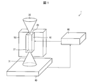
- FIG. 1 is a schematic diagram showing a schematic configuration of the optical sensor system 1.
- the optical sensor system 1 includes a semiconductor laser 10, a photodiode 40 (light emission detection unit), a submount 50, and a control arithmetic device 60 (environment parameter calculation unit).
- Semiconductor laser 10 is an element that emits laser light when current is injected. In general, since a semiconductor laser is small and inexpensive, it is suitable as a light source for the optical sensor system 1 of the present invention. As shown in FIG. 1, the semiconductor laser 10 includes a front surface 20 (second light emitting surface) and a rear surface 21 (first light emitting surface). Both the front surface 20 and the rear surface 21 are mirror surfaces. A waveguide (not shown) is formed between the front surface 20 and the rear surface 21.
- the front surface 20 has lower reflectance and higher transmittance than the rear surface 21. Therefore, the front surface outgoing light 30 (first light emission) emitted from the front surface 20 has a higher intensity than the rear surface outgoing light 31 (second light emission) emitted from the rear surface 21.
- the strong front surface outgoing light 30 emitted from the front surface 30 is used for various applications.
- the optical sensor system 1 may include another light source (for example, a fluorescent lamp, an LED, or an HID lamp) instead of the semiconductor laser 10.
- another light source may sequentially emit two types of light (front surface emitted light 30 and rear surface emitted light 31) from one light emitting surface.
- another light source may split one light emitted from one light emitting surface into two types of light.
- the current injected into the semiconductor laser 10 generates photons in the waveguide.
- the generated photons are reflected by the front surface 20 and the rear surface 21 to repeatedly increase and decrease the number of photons in the waveguide while reciprocating in the waveguide and reach a resonance state.
- the front surface emission light 30 and the rear surface emission light 31 are emitted from the front surface 20 and the rear surface 21.
- the front surface outgoing light 30 emitted from the front surface 20 is used for various purposes as a laser light source. Further, the rear surface outgoing light 31 emitted from the rear surface 21 enters the photodiode 40.
- the photodiode 40 is an element that detects the incident rear surface outgoing light 31 and converts the detected value into an electric signal (current signal or voltage signal).
- the photodiode 40 transmits the electrical signal converted from the rear surface outgoing light 31 to the control arithmetic device 60.
- the photodiode 40 can be replaced with another means capable of evaluating the intensity of the rear surface outgoing light 31.
- the submount 50 has a role of fixing the semiconductor laser 10 and releasing heat generated by the semiconductor laser 10 to the outside.
- a ceramic material having high thermal conductivity such as aluminum nitride is generally used.
- the semiconductor laser 10 is bonded to the submount 50 via a solder material such as an Au—Sn alloy solder.
- the control arithmetic device 60 controls the semiconductor laser 10. Further, an environmental parameter (humidity) is calculated from the amplitude of the electric signal received from the photodiode 40 (intensity of the rear surface outgoing light 31). For example, the control arithmetic device 60 may calculate the humidity based on the relationship between the humidity and the light intensity stored in advance in a storage device (not shown).
- the control arithmetic device 60 can be composed of a plurality of chips and a microcomputer. A general-purpose arithmetic device such as a personal computer may be used as the control arithmetic device 60. An example of an environmental parameter calculation method by the control arithmetic device 60 will be described below.
- the control arithmetic device 60 causes the semiconductor laser 10 to emit light by injecting a constant current (ACC) into the semiconductor laser 10. After the light emission intensity of the semiconductor laser 10 is stabilized, the intensity of the rear surface outgoing light 31 is evaluated based on the electric signal received from the photodiode 40. The control arithmetic unit 60 turns off the semiconductor laser 10 immediately after evaluating the intensity of the rear surface outgoing light 31. Then, the humidity is calculated from the obtained evaluation value based on the relationship between the humidity and the light intensity (for example, experimental data shown in FIG. 2) stored in advance in a storage device (not shown).
- ACC constant current
- the emission time of the semiconductor laser 10 is short in the calculation method of the environmental parameter.
- the control arithmetic device 60 does not need to drive the semiconductor laser 10 with a constant current (ACC).
- the control arithmetic device 60 may drive the semiconductor laser 10 at a constant output (APC) so that the intensity of the rear surface outgoing light 31 is constant.
- APC constant output
- the control arithmetic unit 60 calculates the humidity based on the current value of the injection current to the semiconductor laser 10 when the intensity of the rear surface outgoing light 31 becomes substantially constant.
- the front surface emission light 30 can be used not only for various purposes as a normal laser light source but also the rear emitted together with the front surface emission light 30.
- An environmental parameter can be calculated based on the intensity of the emitted light 31.
- a semiconductor laser 10 for an optical recording apparatus was used.
- This semiconductor laser 10 has an oscillation wavelength of 660 nm and a maximum output of 150 mW.
- the reflectance of the semiconductor laser 10 on the waveguide side of the front surface 20 and the reflectance of the rear surface 21 on the waveguide side are approximately 6% (transmittance is approximately 94%) and approximately 90% (transmittance is approximately 10%).
- the reflectance at each end face of the semiconductor laser 10 is defined by the multilayer structure of the multilayer mirror formed on the end face.
- the reflectance of the end face varies depending on the refractive index and the number of layers of the material constituting the multilayer structure.
- the front surface outgoing light 30 emitted from the front surface 20 having a low reflectance and a high transmittance is higher in intensity than the rear surface outgoing light 31 emitted from the rear surface 21 having a high reflectance and a low transmittance.
- the front surface outgoing light 30 is used for recording information on the optical storage medium and reproducing information from the optical storage medium.
- FIG. 2 shows experimental data representing changes in the intensity of the front surface outgoing light 30 and the rear surface outgoing light 31 with respect to changes in humidity.
- the humidity and the intensity of the rear surface outgoing light 31 have a substantially proportional relationship.
- the humidity increases from 23% to 62%, the intensity of the rear surface outgoing light 31 increases by about 8.7%.
- the control arithmetic device 60 described above can calculate the humidity from the intensity of the rear surface outgoing light 31 by utilizing the proportional relationship between the intensity of the rear surface outgoing light 31 and the humidity.
- the intensity of the front surface outgoing light 30 is substantially constant regardless of the humidity (the difference between the maximum value and the minimum value of the intensity is about 0.35%).
- the amount of change in the intensity of the front surface outgoing light 30 (0.35%) is 1/20 or less of the amount of change in the intensity of the rear surface outgoing light 31 (8.7%). Therefore, the front surface outgoing light 30 can be used for various purposes such as recording or reproducing information on an optical recording medium without considering the influence of changes in humidity.
- the humidity around the semiconductor laser 10 changes, the amount of moisture adsorbed on the front side (surface exposed to the outside) of the front surface 20 and the rear surface 21 changes. As a result, the refractive indexes of the front surface 20 and the rear surface 21 change. As the refractive index of the front surface 20 and the rear surface 21 is changed, the transmittance and the reflectance of each surface are changed.
- the front surface 20 is designed to have a high transmittance (about 94%). Therefore, when the transmittance of the front surface 20 slightly changes due to a change in humidity, the intensity of the front surface outgoing light 30 does not change much. That is, when the humidity changes, the rate of change in the intensity of the rear surface outgoing light 31 is small.
- the rear surface 21 is designed to have a low transmittance (about 10%). Therefore, when the transmittance of the rear surface 21 slightly changes due to a change in humidity, the intensity of the rear surface outgoing light 31 changes greatly. That is, when the humidity changes, the rate of change of the intensity of the rear surface outgoing light 31 is large.
- the rear surface 21 is designed to have a higher reflectance. However, it is difficult to design the rear surface 21 having an excessively high reflectance. In addition, the manufacturing cost of the semiconductor laser 10 provided with the rear surface 21 having such a high reflectance also increases. Therefore, it is sufficient that the rear surface 21 has a reflectance of 85% or more from the viewpoint of the ease of designing the rear surface 21 and the low cost of the semiconductor laser 10.
- the intensity of the semiconductor laser 10 varies depending on factors such as heat generation or deterioration.
- the intensity of the semiconductor laser 10 changes due to these factors, the intensity of the front surface outgoing light 30 and the rear surface outgoing light 31 also changes.
- the intensity of the front surface outgoing light 30 does not depend on humidity (see FIG. 2). Therefore, it is considered that the intensity of the front surface outgoing light 30 depends only on the above factors.
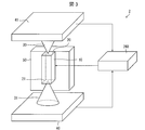
- FIG. 3 is a schematic diagram showing a schematic configuration of the optical sensor system 2 according to the present embodiment.
- the optical sensor system 2 includes a semiconductor laser 10, a photodiode 40, a second photodiode 41 (second detection unit), a submount 50, and a control arithmetic device 260.
- the second photodiode 41 detects the laser light incident on the second photodiode 41 and converts the detected value into an electrical signal.
- the front surface emission light 30 emitted from the front surface 20 of the semiconductor laser 10 is incident on the second photodiode 41.
- the second photodiode 41 converts the detected value of the light emitted from the front surface 30 into an electrical signal (current signal or voltage signal) and transmits the electrical signal to the control arithmetic device 260.
- Control arithmetic unit 260 controls semiconductor laser 10. In addition, electrical signals are received from the photodiode 40 and the second photodiode 41, respectively.
- the control arithmetic unit 260 can be composed of a plurality of chips and a microcomputer. A general-purpose arithmetic device such as a personal computer may be used as the control arithmetic device 260.
- the control arithmetic unit 260 evaluates the intensity of the front surface outgoing light 30 from the amplitude of the electric signal detected by the second photodiode 41. Further, the intensity of the rear surface outgoing light 31 is evaluated from the amplitude of the electrical signal detected by the photodiode 40. Thereafter, the intensity of the rear surface outgoing light 31 is corrected based on the intensity of the front surface outgoing light 30. Then, the control arithmetic device 260 calculates an environmental parameter (humidity) based on the corrected intensity of the rear surface outgoing light 31. An example of an environmental parameter calculation method by the control arithmetic device 260 will be described below.
- the control arithmetic unit 260 causes the semiconductor laser 10 to emit light by injecting a certain amount of current into the semiconductor laser 10. After the light emission intensity of the semiconductor laser 10 is stabilized, the control arithmetic device 260 evaluates the intensity of the rear surface outgoing light 31 based on the electric signal received from the photodiode 40. Further, based on the current signal received from the second photodiode 41, the intensity of the front surface outgoing light 30 is evaluated. The control arithmetic unit 260 turns off the semiconductor laser 10 after evaluating the intensity of the front surface outgoing light 30.
- the control arithmetic unit 260 calculates the ratio between the intensity of the rear surface outgoing light 31 and the intensity of the front surface outgoing light 30.
- the intensity of the semiconductor laser 10 changes, the intensity of the front surface outgoing light 30 and the intensity of the rear surface outgoing light 31 change at the same rate. Therefore, by dividing the intensity of the rear surface outgoing light 31 by the intensity of the front surface outgoing light 30, changes due to the above factors are removed from the intensity of the rear surface outgoing light 31. Thereby, the intensity
- the control arithmetic unit 260 is divided by the intensity of the front surface outgoing light 30 with reference to the above relationship (relationship between the intensity of the rear surface outgoing light 31 and the humidity divided by the intensity of the front surface outgoing light 30). Based on the intensity of the rear surface outgoing light 31, the environmental parameter (humidity) is calculated.
- control arithmetic device 260 calculates the environmental parameter (humidity) by the following method.
- the relationship between the intensity of the rear surface outgoing light 31 and the humidity when the intensity of the front surface outgoing light 30 is a predetermined value is evaluated in advance.
- the control arithmetic unit 260 causes the semiconductor laser 10 to emit light by injecting a current into the semiconductor laser 10, and evaluates the intensity of the front surface emission light 30 from the electrical signal received from the second photodiode 41.
- the control arithmetic unit 260 controls the current value of the injection current to the semiconductor laser 10 so that the intensity of the front surface outgoing light 30 becomes the predetermined value.
- the control arithmetic unit 260 evaluates the intensity of the rear surface outgoing light 31 from the electrical signal received from the photodiode 40 when the intensity of the front surface outgoing light 30 reaches a predetermined value. Then, after evaluating the intensity of the rear surface outgoing light 31, the semiconductor laser 10 is turned off immediately.
- control arithmetic unit 260 determines the relationship between the intensity and humidity of the rear surface outgoing light 31 (the intensity and humidity of the rear surface outgoing light 31 when the intensity of the front surface outgoing light 30 is a predetermined value).
- the humidity is calculated based on the intensity of the rear surface outgoing light 31 with reference to FIG.
- the intensity of the rear surface outgoing light 31 is corrected by the intensity of the front surface outgoing light 30 that depends only on factors other than environmental parameters (humidity).
- the intensity of the rear surface outgoing light 31 does not depend on factors (heat generation or deterioration of the semiconductor laser 10) other than the environmental parameter (humidity). Therefore, the control arithmetic unit 260 can accurately calculate the environmental parameter based on the intensity of the rear surface outgoing light 31 that depends only on the environmental parameter.
- the optical sensor system 3 calculates the gas concentration as an environmental parameter. That is, in this embodiment, the gas concentration is a sensing target.
- FIG. 4 is a schematic diagram showing a schematic configuration of the optical sensor system 3 according to the present embodiment.
- the optical sensor system 3 includes a semiconductor laser 10, a photodiode 40, a submount 50, a control arithmetic device 360, and a gas sensitive film 70.
- the gas sensitive film 70 is a thin film having optical characteristics (refractive index or transmittance of laser light) that change depending on a specific type of gas concentration. As shown in FIG. 4, the gas sensitive film 70 is disposed on the rear surface 21 of the semiconductor laser 10. Depending on the specific gas concentration, the refractive index or transmittance of the gas sensitive film 70 changes. Therefore, depending on the specific gas concentration, the intensity of the rear surface outgoing light 31 that passes through the gas sensitive film 70 increases or decreases.
- the material of the gas sensitive film 70 for example, various polymer materials that expand (swell) by absorbing a VOC (Volatile Organic Compound) gas in the air and change the refractive index can be used.
- various oxide materials or catalyst materials that cause an oxidation-reduction reaction or catalytic reaction with a specific gas and change the refractive index or transmittance may be used.
- the material and shape of the gas sensitive film 70 are not limited as long as the intensity of the rear emission light 31 transmitted through the gas sensitive film 70 can be changed depending on a specific gas concentration.
- a moisture blocking film that blocks moisture is provided between the rear surface 21 and the gas sensitive film 70.
- a moisture barrier film for example, a nitride thin film such as a SiN thin film or an AlN thin film can be used.
- the control arithmetic device 360 controls the semiconductor laser 10. In addition, an electrical signal representing the intensity of the rear surface outgoing light 31 is received from the photodiode 40, and an environmental parameter (gas concentration) is calculated from the received electrical signal.
- the control arithmetic device 360 can be composed of a plurality of chips and a microcomputer.
- a general-purpose arithmetic device such as a personal computer may be used as the control arithmetic device 360.
- the control arithmetic device 360 may calculate the humidity based on the relationship between the gas concentration and the light intensity stored in advance in a storage device (not shown).
- a specific gas concentration can be calculated as the environmental parameter.
- the optical sensor system 1 has the same configuration as the optical sensor system 1 (see FIG. 1) described in the first embodiment.
- FIG. 5 is a schematic diagram showing the emission characteristics (relationship between injection current and emission intensity) of a semiconductor laser according to the reference.
- the semiconductor laser 10 provided in the optical sensor system 1 according to the present embodiment also has the same light emission characteristics as the semiconductor laser according to the reference.
- the emission characteristics of the semiconductor laser according to the reference are roughly classified into two regions with the oscillation threshold 80 as a boundary.
- the injection current to the semiconductor laser is smaller than the oscillation threshold value 80, the number of photons is not sufficiently amplified in the resonator (waveguide and two mirror surfaces) of the semiconductor laser, so that laser oscillation does not occur. Therefore, laser light is not emitted from the semiconductor laser, but only light generated based on the same principle as that of the LED is emitted. Therefore, when the injection current is smaller than the oscillation threshold 80, the intensity of light emission of the semiconductor laser is small.
- the injection current is larger than the oscillation threshold value 80
- the number of photons is sufficiently amplified in the resonator, and laser oscillation occurs.
- laser light is emitted from the semiconductor laser.
- the intensity of light emitted from the semiconductor laser is high.
- the intensity of light emission of the semiconductor laser is almost proportional to the injection current. That is, the relationship between the emission intensity of the semiconductor laser and the injection current can be expressed by a linear equation.
- the linear intercept is defined as the oscillation threshold value 80.
- the slope of the same linear equation (the amount of increase in emission intensity per unit injection current) is called differential efficiency 81.
- control arithmetic unit 360 causes the semiconductor laser 10 to emit laser light by injecting a current having a current value (first current value) sufficiently larger than the oscillation threshold 80 into the semiconductor laser 10.
- the control arithmetic unit 360 evaluates the intensity (first intensity) of the rear surface outgoing light 31 based on the electrical signal received from the photodiode 40 after the emission intensity of the semiconductor laser 10 is stabilized. Then, the correspondence relationship between the first intensity and the first current value is stored in a storage device (not shown). The control arithmetic device 360 turns off the semiconductor laser 10 immediately after the evaluation of the intensity of the rear surface outgoing light 31 is completed.
- control arithmetic unit 60 injects into the semiconductor laser 10 a current having a current value (second current value) that is sufficiently larger than the oscillation threshold 80 and different from the first current value.
- the control arithmetic unit 360 evaluates the intensity (second intensity) of the rear surface outgoing light 31 based on the electrical signal received from the photodiode 40 after the intensity of light emitted from the semiconductor laser 10 is stabilized. Then, the correspondence relationship between the second intensity and the second current value is stored in the storage device.
- the control arithmetic unit 360 repeats the above operation, thereby the intensity of the rear surface outgoing light 31 (first intensity, second intensity, etc) and the current value of the injection current to the semiconductor laser 1 (first intensity). A plurality of data indicating a correspondence relationship with the current value, the second current value, etc) is acquired. Then, the control arithmetic unit 360 performs a least-square fitting process on the obtained plurality of data, thereby expressing a relationship between the intensity of the rear surface outgoing light 31 and the injection current to the semiconductor laser 10. Is calculated.
- the calculated linear intercept is the oscillation threshold 80 and the slope is the differential efficiency 81.
- the above calculation method is an example.
- the control arithmetic device 360 may calculate the oscillation threshold 80 and the differential efficiency 81 by another calculation method.
- the control arithmetic device 360 calculates environmental parameters (temperature and humidity) based on the intensity of the rear surface outgoing light 31 using the calculated oscillation threshold 80 and differential efficiency 81.
- control arithmetic device 360 calculates environmental parameters (temperature and humidity) by the following method.
- FIG. 6 (a) to 6 (d) are experimental data showing temperature dependency and humidity dependency of the oscillation threshold 80 and the differential efficiency 81 of the rear surface outgoing light 31.
- FIG. 6 (a) to 6 (d) are experimental data showing temperature dependency and humidity dependency of the oscillation threshold 80 and the differential efficiency 81 of the rear surface outgoing light 31.
- FIG. 6 (a) and 6 (b) show the temperature dependence and humidity dependence of the oscillation threshold 80, respectively. As shown in FIG. 6A, as the temperature rises, the oscillation threshold 80 increases monotonously. Further, as shown in FIG. 6B, the oscillation threshold 80 hardly depends on humidity.
- the control arithmetic unit 360 calculates the temperature based on the temperature dependence of the oscillation threshold 80 shown in FIG.
- 6 (c) and 6 (d) show the temperature dependence and humidity dependence of the differential efficiency 81, respectively.
- the differential efficiency 81 decreases almost linearly as the temperature increases.
- the differential efficiency 81 decreases almost linearly as the humidity increases.
- the control arithmetic unit 360 calculates the humidity based on the previously calculated temperature and the humidity dependency of the differential efficiency 81 shown in FIG. 6D (or FIG. 6C).
- control arithmetic device 360 may use a temperature detected by a temperature sensor (not shown) mounted on the optical sensor system 1 when calculating the humidity.
- the control arithmetic device 360 can calculate a plurality of environmental parameters (temperature and humidity). Therefore, the added value of the optical sensor system 1 including the control arithmetic device 360 is improved as compared with the optical sensor system 1 including the control arithmetic device 60 of the first embodiment.
- optical gas sensor system 100 including the optical sensor system 1 according to the first embodiment will be described.
- the optical gas sensor system 100 is a device that senses a specific gas concentration.
- the optical gas sensor system 100 may include the optical sensor system 3 according to the third embodiment instead of the optical sensor system 1.
- FIG. 7 is a schematic diagram showing a schematic configuration of the optical gas sensor system 100 according to the present embodiment.
- the optical gas sensor system 100 includes an optical sensor system 1, a gas reactant 110, lenses 120A and 120B, a photodetector 130 (transmitted light detection unit), and a control arithmetic device 140 (gas detection unit). It has.
- the gas reactant 110 is a structure having optical characteristics that change depending on the concentration of a specific gas existing around the optical gas sensor system 100.
- the gas reactant 110 may be, for example, a structure whose refractive index or transmittance changes according to a change in gas concentration.
- the gas reactant 110 has a structure that changes the reflectance or birefringence when the gas concentration changes, or causes a wavelength shift in the light incident on the gas reactant 110 (front emission light 30 ′). It may be a body.
- various polymer materials that expand (swell) by absorbing a VOC gas in the air and change the refractive index can be used.
- various oxide materials or catalyst materials that cause an oxidation-reduction reaction or catalytic reaction with a specific gas and change the refractive index or transmittance can be used.
- the material and shape of the gas reactant 110 are not limited as long as the intensity of the front emission light 30 ′ transmitted through the gas reactant 110 can be changed depending on the specific gas concentration.
- the lens 120A collimates the front emission light 30 emitted from the optical sensor system 1.
- the front emission light 30 ′ collimated by the lens 120 ⁇ / b> A enters the gas reactant 110.
- the lens 120 ⁇ / b> B collects the transmitted light 150 transmitted through the gas reactant 110 on the photodetector 130.
- the photodetector 130 is a device that detects the transmitted light 150 collected by the lens 120B.
- various photoelectric conversion devices such as a photodiode or a CdS cell can be used.
- the photodetector 130 converts the detected value of the transmitted light 150 into an electric signal (current signal or voltage signal) and transmits the electric signal to the control arithmetic device 140.
- the control arithmetic device 140 controls the optical sensor system 1. Further, the specific gas concentration is calculated based on the electrical signal received from the photodetector 130.
- the control arithmetic device 140 can be composed of a plurality of chips and a microcomputer. Further, a general-purpose arithmetic device such as a personal computer may be used as the control arithmetic device 140. Alternatively, the control arithmetic device 140 may constitute one device together with the control arithmetic device 60 of the optical sensor system 1. Hereinafter, the operation of the control arithmetic device 140 will be described.
- control arithmetic device 140 causes the semiconductor laser 10 to emit light by controlling the optical sensor system 1. Thereby, the front surface outgoing light 30 is emitted from the optical sensor system 1.
- the front surface outgoing light 30 emitted from the optical sensor system 1 is collimated by the lens 120 ⁇ / b> A and enters the gas reactant 110.
- a part of the front surface outgoing light 30 ′ (transmitted light 150) incident on the gas reactant 110 passes through the gas reactant 110.
- the optical characteristic (refractive index or transmittance) of the gas reactant 110 changes depending on the specific gas concentration
- the intensity of the transmitted light 150 changes depending on the specific gas concentration.
- the transmitted light 150 is collected by the lens 120 ⁇ / b> B and enters the photodetector 130.
- the photodetector 130 detects the incident transmitted light 150 and converts the detected value of the transmitted light 150 into an electrical signal. Then, the converted electric signal is transmitted to the control arithmetic device 140.
- the control arithmetic unit 140 evaluates the intensity of the transmitted light 150 from the amplitude of the electrical signal received from the photodetector 130. Then, referring to the relationship between the intensity of the transmitted light 150 and the specific gas concentration, the specific gas concentration is calculated based on the evaluated intensity of the transmitted light 150.
- control arithmetic unit 60 of the optical sensor system 1 calculates environmental parameters such as temperature, humidity, or gas concentration from the intensity of the rear surface outgoing light 31 as described in the first embodiment.
- the control arithmetic unit 60 calculates the gas concentration as in the third embodiment
- the gas that reacts with the gas reaction film 70 (see FIG. 4) and the gas that reacts with the gas reactant 110 are mutually It can be a different gas.
- the intensity of the transmitted light 150 detected by the photodetector 130 changes as the temperature or humidity changes. That is, the intensity of the transmitted light 150 detected by the photodetector 130 depends not only on the gas concentration but also on temperature or humidity. Therefore, an error (noise) occurs in the gas concentration calculated based on the intensity of the transmitted light 150.
- the control arithmetic device 140 may correct the gas concentration calculated based on the intensity of the transmitted light 150 based on the temperature or humidity calculated by the optical sensor system 1. With the above configuration, the control arithmetic device 140 can calculate the gas concentration with higher accuracy. In the above configuration, the relationship between the gas concentration and the intensity of the transmitted light 150 when the temperature or humidity is a predetermined value is obtained in advance.
- control arithmetic device 140 calculates the amount of change in the intensity of the transmitted light 150 when the gas concentration remains constant and the temperature or humidity changes from the predetermined value to the temperature or humidity calculated by the optical sensor system 1. To do. The amount of change depends on the temperature or humidity calculated by the optical sensor system 1.
- control arithmetic device 140 subtracts the amount of change from the intensity of the transmitted light 150 detected by the photodetector 130.
- the intensity of the transmitted light 150 after subtraction depends only on the gas concentration.
- control arithmetic device 140 refers to the above relationship (the relationship between the gas concentration and the intensity of the transmitted light 150 when the temperature or the humidity is a predetermined value), and thereby based on the intensity of the transmitted light 150 after subtraction.
- the gas concentration is calculated.
- the optical gas sensor system 100 can not only sense a specific gas concentration, but also can sense environmental parameters such as temperature, humidity, or gas concentration by the optical sensor system 1. That is, the optical gas sensor system 100 is a multi-sensing device.
- the optical gas sensor system 100 has a high added value as compared with the conventional optical gas sensor system that can only sense a specific gas concentration.
- the optical gas sensor system 100 can reduce the number of parts compared to a conventional optical gas sensor system that needs to additionally include a sensor for sensing environmental parameters. Therefore, the optical gas sensor system 100 can reduce the cost of parts, the transportation cost of parts, and the assembly cost of parts.
- the optical gas sensor system 100 may include a sample holder in which an arbitrary sample can be placed instead of the gas reactant 110.
- the sample holder is disposed at the position of the gas reactant 110 in FIG.
- the optical gas sensor system 100 can be used as a transmittance measuring device that measures the transmittance of a sample.
- the particle sensor system 200 including the optical sensor system 1 according to the first embodiment will be described.
- the fine particle sensor system 200 is a device that detects fine particles (dust) floating in the air.
- the particle sensor system 200 may include the optical sensor system 3 according to the third embodiment instead of the optical sensor system 1.
- FIG. 8 is a schematic diagram showing a schematic configuration of the particle sensor system 200 according to the present embodiment.
- the particle sensor system 200 includes an optical sensor system 1, a lens 210, a photodetector 220 (scattered light detector), and a control arithmetic device 230 (particle detector).
- the lens 210 collimates the front emission light 30 emitted from the optical sensor system 1.
- the front emission light 30 ′ made parallel by the lens 210 enters the detection region 240.
- the photodetector 220 detects the incident scattered light 260. Then, the photodetector 220 converts the detected value of the scattered light 260 into an electric signal (current signal or voltage signal), and transmits the converted electric signal to the control arithmetic device 230.
- the photodetector 220 for example, various photoelectric conversion devices such as a photodiode or a CdS cell can be used.
- the control arithmetic device 230 controls the optical sensor system 1. Further, the intensity of the scattered light 260 is evaluated based on the amplitude of the electrical signal received from the photodetector 220. Then, based on the evaluated intensity of the scattered light 260, it is determined whether or not the fine particles 250 are present in the detection region 240. For example, when the intensity of the scattered light 260 is equal to or greater than a predetermined value, the control arithmetic device 230 may determine that the fine particles 250 are included in the detection region 240.
- the control arithmetic unit 230 calculates (evaluates) the content of the fine particles 250 included in the detection region 240 based on the intensity of the scattered light 260 when the fine particles 250 exist in the detection region 240.
- the control arithmetic unit 230 can be composed of a plurality of chips and a microcomputer. Further, a general-purpose arithmetic device such as a personal computer may be used as the control arithmetic device 230. Alternatively, the control arithmetic device 230 may constitute one device together with the control arithmetic device 60 of the optical sensor system 1.
- the control arithmetic unit 60 of the optical sensor system 1 calculates environmental parameters such as temperature, humidity, or gas concentration based on the intensity of the rear surface outgoing light 31 as described in the first embodiment.
- environmental parameters such as temperature, humidity, or gas concentration based on the intensity of the rear surface outgoing light 31 as described in the first embodiment.
- the control arithmetic unit 60 causes the semiconductor laser 10 to emit light in order to calculate the environmental parameters, part or all of the emitted light enters the detection region 240 as the front surface emission light 30 ′.
- the front surface emission light 30 ' causes the semiconductor laser 10 to emit light in order to calculate the environmental parameters. In this case, it is preferable to use the front surface outgoing light 30 ') incident on the detection region 240. In this configuration, while the semiconductor laser 10 emits once, the environmental parameters are calculated by the control arithmetic device 60, and the content of the fine particles 250 in the detection region 240 is evaluated by the control arithmetic device 230. .
- control arithmetic device 60 and the control arithmetic device 230 it is not necessary for the control arithmetic device 60 and the control arithmetic device 230 to emit the semiconductor laser 10 repeatedly. Further, the accumulated light emission time of the semiconductor laser 10 is suppressed. As a result, the lifetime of the semiconductor laser 10, the optical sensor system 1, and the particulate sensor system 200 is extended. Further, the power consumption of the particle sensor system 200 is reduced.
- the fine particle sensor system 200 can not only detect fine particles floating in the air (detection region 240), but also calculates environmental parameters such as temperature, humidity, or gas concentration by the optical sensor system 1. be able to. That is, the particle sensor system 200 is a multi-sensing device capable of sensing a plurality of objects related to air quality and safety.
- the particle sensor system 200 has a high added value as compared with the conventional particle sensor system that can only detect particles floating in the air. Further, since the particle sensor system 200 does not need to additionally include a sensor for sensing environmental parameters, the number of parts can be reduced as compared with the conventional particle sensor system. As a result, the particle sensor system 200 can reduce the cost of parts, the cost of transporting parts, and the cost of assembling parts.
- the particle sensor system 200 may include a sample holder that can place an arbitrary sample in the detection region 240.
- the particle sensor system 200 can be used as a transmittance measuring device that measures the transmittance of a sample placed in a sample holder.
- FIG. 9 is a schematic diagram illustrating a schematic configuration of the air purifier 201.
- the air purifier 201 includes a particulate sensor system 200, an air purification filter 270, an air intake 280, and an air outlet 290.
- the air purification filter 270 removes contaminants such as fine particles and gas contained in the air flowing into the air purifier 201 through the air intake port 280.
- the air cleaning filter 270 may be, for example, a HEPA filter (High Efficiency Particulate Air Filter).
- the air purifying filter 270 may clean the air by jetting water into the air that has flowed into the air purifier 201 or submerging the air into the water.
- the air purified by passing through the air cleaning filter 270 is sent to the air outlet 290.
- the air intake port 280 takes ambient air into the air purifier 201 and supplies the taken air to the air purification filter 270.
- the air outlet 290 blows out air from which contaminants have been removed by passing through the air purifying filter 270 to the outside of the air purifier 201.
- the air cleaner 201 may have a humidification function and a dehumidification function.
- the air purifier 201 may control the height of the humidifying ability and the dehumidifying ability based on the humidity (environmental parameter) calculated by the optical sensor system 1 mounted on the particulate sensor system 200.
- the air purifier 201 may control the height of the air cleaning capability based on the amount of fine particles detected by the fine particle sensor system 200.
- the air cleaner 201 displays the amount of fine particles detected by the fine particle sensor system 200 or the environmental parameter calculated by the optical sensor system 1 on a display unit (not shown), and thereby the air state and The user may be notified of safety.
- the air purifier 201 operates based only on the result of sensing by the particulate sensor system 200 or the optical sensor system 1. Therefore, the fine particle sensor system 200 does not need to include a plurality of sensors in order to realize the above operation. Therefore, the particle sensor system 200 can reduce the number of parts and reduce the cost of parts, the transportation cost of parts, and the assembly cost of parts compared to a conventional particle sensor system having a plurality of sensors. it can.
- the light emitting device 300 including the optical sensor system 1 according to the first embodiment will be described.
- the light emitting device 300 is a device that emits laser light generated by the semiconductor laser 10 included in the optical sensor system 1 to the outside.
- the light emitting device 300 controls the light emission condition of the semiconductor laser 10 based on the result of the environmental parameter calculated by the optical sensor system 1.
- the light emitting device 300 may include the optical sensor system 3 according to the third embodiment instead of the optical sensor system 1.
- FIG. 10 is a schematic diagram showing a schematic configuration of the light emitting device 300 according to the present embodiment.
- the light emitting device 300 includes the optical sensor system 1, a case 310, a temperature regulator 320, and a control arithmetic device 330 (light emission condition control unit).
- the optical sensor system 1 calculates environmental parameters (temperature, humidity, gas concentration), and transmits the calculated environmental parameters to the control arithmetic device 330.
- Case 310 protects the entire optical sensor system 1.
- the case 310 particularly protects the semiconductor laser 10 included in the optical sensor system 1.
- the case 310 is generally made of resin, metal, glass or the like.
- the case 310 is provided with a window for drawing out the front surface outgoing light 30 emitted from the semiconductor laser 10 to the outside of the case 310.
- the front surface outgoing light 30 drawn to the outside is used for various applications.
- the semiconductor laser 10 is classified into a type used in a state where it is open to the atmosphere and a type used in a state sealed in pure nitrogen or pure air not containing humidity.
- the semiconductor laser 10 is a product that is used in a state that is open to the atmosphere, the case 310 need not be sealed. In the above case, the inside of the case 310 is opened to the atmosphere.
- the case 310 is strictly sealed.
- the inside of the case 310 is filled with pure nitrogen or pure air.
- the temperature adjuster 320 adjusts the temperature of the optical sensor system 1 so that the temperature of the optical sensor system 1 matches a preset temperature. Further, the heat generated from the optical sensor system 1 is discharged to the outside.
- the set temperature of the optical sensor system 1 may be set by a user or may be set by the control arithmetic device 320.
- the temperature regulator 320 may be composed of, for example, a Peltier element or a fin. When the temperature regulator 320 is composed of Peltier elements, the temperature of the optical sensor system 1 can be strictly controlled.
- the temperature regulator 320 can cool the temperature of the optical sensor system 1 to a temperature below the environment. When the temperature of the optical sensor system 1 becomes equal to or lower than the temperature of the environment, condensation may occur in the optical sensor system 1.
- the control arithmetic device 330 controls the optical sensor system 1. Further, based on the environmental parameters (peripheral parameters) received from the optical sensor system 1, the set temperature of the temperature regulator 320 and the light emission conditions of the semiconductor laser 10 are controlled.
- the control arithmetic device 330 can be composed of a plurality of chips and a microcomputer. Further, a general-purpose arithmetic device such as a personal computer may be used as the control arithmetic device 330. Alternatively, the control arithmetic device 330 may constitute one device together with the control arithmetic device 60 of the optical sensor system 1.
- the semiconductor laser 10 is not manufactured on the assumption that it is used in a high humidity environment. Therefore, the semiconductor laser 10 has a very high possibility of failure when used in a high humidity environment.
- the temperature of the optical sensor system 1 is lower than the dew point, condensation may occur in the optical sensor system 1.
- condensation occurs in the optical sensor system 1 and water droplets adhere to the semiconductor laser 10, the water droplets cause a failure of the semiconductor laser 10.
- the control arithmetic unit 330 operates so as to solve these problems. Hereinafter, the operation of the control arithmetic device 330 will be described.
- control arithmetic unit 330 The operation of the control arithmetic unit 330 differs depending on the type of the semiconductor laser 10 and whether or not the case 310 is sealed. More specifically, the operation of the control arithmetic unit 330 is as follows: (1) The semiconductor laser 10 is a type used in a state of being sealed in pure nitrogen or pure air, and the case 310 is sealed (2) The semiconductor laser 10 is a type used in a state where the semiconductor laser 10 is open to the atmosphere, and differs from the case where the case 310 is not sealed.
- control arithmetic device 330 determines whether or not the case 310 has a sealing breakage based on the humidity level detected by the optical sensor system 1. Further, when the humidity calculated by the optical sensor system 1 is higher than a predetermined upper limit value, the light emission of the semiconductor laser 10 is stopped.
- the control arithmetic device 330 will be described in more detail.
- the control arithmetic unit 330 causes the semiconductor laser 10 to emit light by controlling the optical sensor system 1.
- the optical sensor system 1 detects the humidity (environment parameter) around the optical sensor system 1 while the control arithmetic device 330 is emitting the semiconductor laser 10.
- the optical sensor system 1 notifies the control arithmetic device 330 of the detected humidity.
- the case 310 when the case 310 is not broken, the inside of the case 310 is kept in a low humidity state.
- the sealing breakage occurs in the case 310, moisture contained in the atmosphere (outside the case 310) flows into the case 310. Therefore, when the case 310 has a sealing break, the humidity detected by the optical sensor system 1 becomes high.
- the control arithmetic device 330 When the humidity notified from the optical sensor system 1 is equal to or lower than the predetermined upper limit value, the control arithmetic device 330 continues to emit the semiconductor laser 10. On the other hand, when the humidity notified from the optical sensor system 1 is higher than a predetermined upper limit value, the control arithmetic device 330 stops the light emission of the semiconductor laser 10.
- control arithmetic unit 330 can prevent the semiconductor laser 10 from continuously emitting light in a high humidity environment. As a result, the possibility of failure of the semiconductor laser 10 is reduced.
- the light emitting device 300 may include a display device and display on the display device that the case 310 has been broken. In this configuration, the light emitting device 300 can prompt the user to reseal the case 310 and replace each component of the case 310.
- the temperature regulator 320 is assumed to be composed of Peltier elements.
- the control arithmetic unit 330 causes the semiconductor laser 10 to emit light by controlling the optical sensor system 1. While the control arithmetic unit 330 emits the semiconductor laser 10, the optical sensor system 1 detects the humidity (environment parameter) around the optical sensor system 1 using the rear surface outgoing light 31. The optical sensor system 1 notifies the control arithmetic device 330 of the detected humidity.
- the control arithmetic device 330 calculates the temperature (dew point) at which dew condensation occurs in the optical sensor system 1 based on the humidity notified from the optical sensor system 1 and the set temperature of the temperature regulator 320. When the set temperature of the temperature regulator 320 is above the dew point, the control arithmetic unit 330 continues to emit light from the semiconductor laser 10, while when the set temperature of the temperature regulator 320 is below the dew point, Stop flashing.
- control arithmetic unit 330 can prevent condensation from occurring in the optical sensor system 1. As a result, the possibility of failure of the semiconductor laser 10 is reduced.
- control arithmetic device 330 may increase the set temperature of the temperature adjuster 320 when the set temperature of the temperature adjuster 320 is below the dew point. Thereby, since the temperature of the optical sensor system 1 rises, it becomes difficult for condensation to occur in the optical sensor system 1.
- the light emitting device 300 controls the light emission conditions of the semiconductor laser 10 based on the environmental parameters calculated by the optical sensor system 1. As a result, it is possible to prevent the semiconductor laser 10 from failing or dew condensation from occurring in the optical sensor system 1.
- the light emitting device 300 does not need to include a humidity sensor that detects humidity. Therefore, the light-emitting device 300 can reduce the number of parts and the cost of parts, the transportation cost of parts, and the assembly cost of parts compared with the conventional light-emitting device provided with the humidity sensor.
- the optical sensor system 1 may detect not the humidity but the gas concentration of a corrosive gas (such as ozone or chlorine) that causes the failure of the semiconductor laser 10 as the environmental parameter.
- a corrosive gas such as ozone or chlorine
- the arithmetic control device 330 controls the light emission conditions of the semiconductor laser 10 based on the high gas concentration of the corrosive gas detected by the optical sensor system 1.
- the image printing apparatus 400 including the optical sensor system 1 according to the first embodiment will be described.
- the image printing apparatus 400 is an apparatus having an image printing function for printing an image on the printing paper P.
- the image printing apparatus 400 controls image printing conditions based on environmental parameters calculated by the optical sensor system 1.
- the printing conditions are conditions that define the operation or state of the image printing apparatus 400 when printing an image. Specific examples of printing conditions will be described later.
- the image printing apparatus 400 may include the optical sensor system 3 according to the third embodiment instead of the optical sensor system 1.
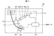
- FIG. 11 is a schematic diagram showing a schematic configuration of the image printing apparatus 400 according to the present embodiment.
- the image printing apparatus 400 includes an optical sensor system 1, a photosensitive drum 410, a charging unit 420, a toner unit 430, a paper feeding unit 440, a fixing unit 450, lenses 460A and 460B, and a control arithmetic device 470 ( A condition control unit).
- the optical sensor system 1 uses a relationship between the current value of the injection current to the semiconductor laser 10 and the intensity of the rear surface outgoing light 31, and uses a plurality of environmental parameters (temperature, Humidity).
- a charged photosensitive sheet is attached to the surface of the photosensitive drum 410.
- the charged photosensitive sheet is neutralized by being irradiated with the front surface outgoing light 30 ′ from the optical sensor system 1.
- a substance such as organic photoreceptor (OPC) or selenium
- OPC organic photoreceptor
- selenium a substance whose electrical conductivity changes when irradiated with light.
- the region not irradiated with light remains charged, while the region irradiated with light changes to an uncharged state.
- an area of the photosensitive sheet that has not been irradiated with light forms an electrostatic latent image drawn with charges.
- the charging unit 420 charges the photosensitive sheet attached to the surface of the photosensitive drum 410.
- a corona discharge method is used to charge the photosensitive sheet.
- a high voltage is applied to the needle-like electrode to cause corona discharge and generate a charge to be added to the photosensitive sheet.
- the toner unit 430 develops the electrostatic latent image formed on the photosensitive sheet of the photosensitive drum 410.
- a magnetic brush developing system is used to develop an electrostatic latent image.
- the toner unit 430 mixes toner particles and magnetic powder (carrier) to attach the toner particles to the carrier, and then removes the carrier to which the toner particles are attached by magnetic force. Stand like a brush. Then, the photosensitive sheet of the photosensitive drum 410 is rubbed with a brush-like carrier. Then, the toner particles adhering to the carrier are combined with charges constituting the electrostatic latent image formed on the photosensitive sheet. Thereby, the electrostatic latent image is developed.
- the paper feeding unit 440 includes two rollers, and sends the printing paper P sandwiched between the rollers toward the photosensitive drum 410 by rotating the rollers.
- the printing paper P sent from the pause unit 440 toward the photosensitive drum 410 comes into contact with the photosensitive sheet on the photosensitive drum 410.
- the toner particles attached to the photosensitive sheet of the photosensitive drum 410 move to the printing paper P.
- an image (developed electrostatic latent image) drawn on the photosensitive sheet of the photosensitive drum 410 is transferred to the printing paper P.
- the fixing unit 450 includes a roller and a heater, and the toner particles are fixed (fixed) to the printing paper by heating the printing paper P with the heater while pressing the printing paper P with the roller.
- the lens 460A collimates the front surface outgoing light 30 emitted from the optical sensor system 1.
- the lens 460B condenses the front surface outgoing light 30 ′ collimated by the lens 460A.
- the front surface outgoing light 30 ′ collected by the lens 460 ⁇ / b> B enters the photosensitive sheet of the photosensitive drum 410.
- Control arithmetic unit 470 controls each unit and optical sensor system 1 provided in image printing apparatus 400. Further, it processes image data received from the outside and receives environmental parameters from the optical sensor system 1.
- the control arithmetic device 470 can be composed of a plurality of chips and a microcomputer. Further, a general-purpose arithmetic device such as a personal computer may be used as the control arithmetic device 470. Alternatively, the control arithmetic device 470 may constitute one device together with the control arithmetic device 60 of the optical sensor system 1.
- control arithmetic unit 470 When the control arithmetic device 470 receives image data from the outside, the control arithmetic device 470 prints the image on the printing paper P in the following procedure.
- control arithmetic device 470 controls the paper feeding unit 440 so as to send the printing paper P toward the photosensitive drum 410. Further, the charging unit 420 charges the photosensitive sheet of the photosensitive drum 410.
- control arithmetic device 470 causes the optical sensor system 1 to emit the front surface emission light 30.
- control arithmetic device 470 draws an electrostatic latent image on the photosensitive sheet of the photosensitive drum 410 by controlling the emission direction of the front surface emission light 30 according to the received image data.
- control arithmetic unit 470 causes the toner unit 430 to develop the electrostatic latent image drawn on the photosensitive sheet of the photosensitive drum 410.
- the image drawn on the photosensitive sheet of the photosensitive drum 410 is transferred to the printing paper P when the printing paper P delivered by the paper supply unit 440 comes into contact with the photosensitive drum 410.
- control arithmetic device 470 controls the fixing unit 450 so that the image transferred onto the printing paper P is fixed on the printing paper P.
- control arithmetic device 470 can adjust the printing conditions based on the environmental parameters (temperature, humidity, etc.) calculated by the optical sensor system 1.
- control arithmetic device 470 may adjust the exposure amount of the photosensitive sheet based on at least one of the temperature and the humidity calculated by the optical sensor system 1.
- control arithmetic device 470 may adjust various printing conditions based on the environmental parameters calculated by the optical sensor system 1.
- the printing conditions that can be adjusted by the control arithmetic unit 470 include (1) the charge amount of the photosensitive sheet on the photosensitive drum 410 and (2) when the image transferred from the photosensitive sheet to the printing paper P is fixed on the printing paper P. And (3) the rotation speed of each roller provided in the image printing apparatus 400, and the like.
- control arithmetic device 470 can improve the quality of printing and reduce the possibility of problems such as paper jams.
- the image printing apparatus 400 need not include a sensor for detecting environmental parameters (temperature, humidity). Therefore, the image printing apparatus 400 reduces the number of parts as compared with the conventional image printing apparatus provided with sensors for detecting environmental parameters (temperature, humidity), the cost of parts, the transportation cost of parts, And the assembly cost of parts can be reduced.
- control arithmetic device 470 may be configured to adjust the print density of the image.
- the print density of the image changes depending on the exposure amount of the photosensitive sheet on the photosensitive drum 410.
- the control arithmetic unit 470 injects a constant injection current into the semiconductor laser 10 and pulses the front surface emission light 30.
- PWM pulse width modulation
- the laser light emitted from the semiconductor laser 10 is subjected to pulse width modulation.
- control arithmetic unit 470 drives the semiconductor laser 10 with a constant injection current using the pulse width modulation method
- control arithmetic unit 60 determines the injection current into the semiconductor laser 10 and the intensity of the rear surface emission light 31. I can't ask for a relationship.
- the laser light emitted from the semiconductor laser 10 is not subjected to pulse amplitude modulation (that is, the semiconductor laser 10 emits an analog wave).
- the optimal driving method of the semiconductor laser 10 differs between the application of the front surface outgoing light 30 and the application of the rear surface outgoing light 31, the optimal driving method may be selected for each application. preferable. That is, when the control arithmetic device 470 exposes the photosensitive sheet of the photosensitive drum 410 using the front surface outgoing light 30, the control arithmetic device 60 drives the semiconductor laser 10 using the pulse width modulation method. On the other hand, when the control arithmetic device 60 calculates the environmental parameter using the rear surface outgoing light 31, the control arithmetic device 60 drives the semiconductor laser 10 using the analog modulation method.
- the optimum light emission conditions of the semiconductor laser 10 are different between the application of the front surface emission light 30 and the application of the rear surface emission light 31, it is preferable that the optimum light emission conditions are selected for each application.
- the light emission conditions include various factors that affect the output of light emission generated by the light emitting device. Specific examples of light emission conditions that can be selected include control temperature, injection current value, driving method (continuous oscillation, pulse oscillation, etc.), and modulation method (analog modulation, PWM modulation, PAM modulation, etc.).
- An optical sensor system (1 to 3) includes an optical sensor including a light emitting device (semiconductor laser 10) that generates a first light emission (front surface emission light 30) used for a predetermined application.
- the light emitting device further generates a second light emission (rear surface emission light 31) and detects the second light emission, and the light emission detection unit detects the second light emission.
- an environmental parameter calculation unit (control arithmetic unit 60) that calculates an environmental parameter that is an index of the environment around the light emitting device using the detected value of the second light emission.
- the environmental parameter is calculated from the detection value of the light emission detection unit that detects the second light emission. Therefore, it is not necessary to additionally provide a sensor for detecting environmental parameters, so that the optical sensor system can be reduced in size and cost.
- the environmental parameter may be, for example, at least one of temperature, humidity, and gas concentration.
- the calculated environmental parameter is utilized for various operations of the optical sensor system.
- the first light emitted from the optical sensor system is used for various purposes different from the calculation of the environmental parameters. Therefore, it is possible to provide an optical sensor system in which the first light emission can be used as a normal light source and the environmental parameter can be calculated by the second light emission.
- the environmental parameter calculation unit calculates the environmental parameter.
- the light emission conditions of the light emitting device in the above and the light emission conditions when the first light emitted to the outside is used for the predetermined application may be different.
- the light emitting device may be a semiconductor laser. Since the semiconductor laser is small and inexpensive, it is suitable as a light source for the optical sensor system according to the present invention.
- the optical sensor system according to Aspect 3 of the present invention is the optical sensor system according to Aspect 1, wherein at least a part of light emission of the light-emitting device when the environmental parameter calculation unit calculates the environmental parameter is the first light emission. It may be used for a predetermined application.
- the second light emission is used to calculate the environmental parameter, and the first light emission can be used for a predetermined application. Therefore, compared to a configuration in which the light emitting device emits light a plurality of times, the cumulative light emission time of the light emitting device can be reduced and the life of the optical sensor system can be extended. Furthermore, the power consumption of the optical sensor system can be reduced.
- the environmental parameter calculation unit may calculate a plurality of the environmental parameters.
- the added value of the optical sensor system can be improved as compared with a configuration in which one environmental parameter is calculated.
- the optical sensor system according to aspect 5 of the present invention is the optical sensor system according to any one of the aspects 1 to 4, wherein the environmental parameter calculation unit is detected by the light emission detection unit when a certain amount of current is injected into the light emitting device.
- the environmental parameter may be calculated based on the detected value of the second light emission.
- the environmental parameter is calculated based on the intensity of the second light emitted from the light emitting device into which a certain amount of current has been injected. Therefore, an inexpensive optical sensor system having a simple configuration can be provided.
- the optical sensor system according to Aspect 6 of the present invention is the optical sensor system according to any one of Aspects 1 to 5, wherein the light emitting device includes a laser light source, and the environmental parameter calculation unit includes the second light emission detection value and the light emission device.
- the oscillation threshold value of the laser light source is calculated from the detection value of the second light emission detected by the light emission detection unit by referring to the correspondence relationship with the oscillation threshold value of the laser light source, and the calculated oscillation threshold value Based on the above, the environmental parameter may be calculated.
- the environmental parameter is calculated based on the light emission oscillation threshold of the light emitting device. Therefore, even when the oscillation threshold value (oscillation condition) changes specifically, the environmental parameter can be calculated with high accuracy based on the changed oscillation threshold value.
- the optical sensor system according to aspect 7 of the present invention is the optical sensor system according to any one of the aspects 1 to 6, wherein the light-emitting device includes a laser light source, and the environmental parameter calculation unit includes the detection value of the second light emission and the above-described value.
- the differential efficiency of the laser light source is calculated from the detected value of the second light emission detected by the light emission detector by referring to the correspondence relationship with the oscillation threshold of the laser light source, and the calculated differential efficiency Based on the above, the environmental parameter may be calculated.
- the environmental parameter is calculated based on the differential efficiency of light emission of the light emitting device. Therefore, even if the differential efficiency (oscillation condition) changes specifically, the environmental parameter can be calculated with high accuracy based on the changed differential efficiency.
- the environmental parameter may be at least one of temperature, humidity, and gas concentration.
- the temperature and humidity that can be used for many operations of the optical sensor system can be calculated as environmental parameters.
- a specific gas concentration that affects the operation and reliability of the light emitting device can be calculated as an environmental parameter.
- An optical sensor system is an optical sensor system including a light emitting device that generates first light emission and second light emission, and includes a light emission detection unit that detects the second light emission, An environmental parameter calculation unit that calculates an environmental parameter that is an index of the environment around the light emitting device using the detection value of the second light emission detected by the light emission detection unit, and the light emitting device includes: A first light emitting surface that emits the first light emission, and a second light emitting surface that emits the second light emission, wherein the first light emitting surface and the second light emitting surface are: When the environmental parameter changes, the change rate of the intensity of the first light emission is configured to be smaller than the change rate of the intensity of the second light emission.
- the second light emission has a relatively large intensity change rate due to a change in environmental parameters. Therefore, the environmental parameter can be evaluated with high sensitivity based on the intensity of the second light emission.
- the first light emission has a relatively small rate of change in intensity due to a change in environmental parameters. Therefore, the first light emission can be used for various purposes as a normal light source. Therefore, it is possible to provide an optical sensor system with high added value that can calculate environmental parameters and can be used as a light source.
- the optical sensor system according to Aspect 10 of the present invention is the optical sensor system according to Aspect 9, wherein the first light emission surface and the second light emission surface have a rate of change in intensity of the first light emission when the environmental parameter changes. However, you may be comprised so that it may become 1/20 or less of the change rate of the intensity
- the change rate of the intensity of the second emission is 1/20 or less of the change rate of the intensity of the first emission.
- the second light emission responds with high sensitivity to changes in the environmental parameters. Therefore, the environmental parameter can be accurately calculated based on the intensity of the second light emission.
- the intensity of the first light emission is almost constant regardless of changes in environmental parameters. Therefore, the first light emission can be used without any problem for the second application even when the environmental parameter changes.
- the first light emitting surface may have a reflectance on the inner side of the light emitting device of 85% or more.
- the oscillation threshold value of the light emitting device can be lowered and the power saving of the system can be realized.
- the intensity of the second light emission changes greatly.
- the high reflectance of the first light emitting surface means that the transmittance of the first light emitting surface is small. Therefore, when the environmental parameter changes, the transmittance of the first light emitting surface changes greatly, and as a result, the intensity of the second light emission also changes greatly. That is, the second light emission responds with high sensitivity to changes in environmental parameters. Therefore, the environmental parameter can be accurately calculated based on the intensity of the second light emission.
- the optical sensor system according to aspect 12 of the present invention further includes a second detection unit that detects the first light emission in any one of the above aspects 1 to 11, and the environmental parameter calculation unit includes the second detection unit.
- the calculation result of the environmental parameter may be corrected based on the detection value of the first light emission by the detection unit.
- the calculation result of the environmental parameter is corrected based on the detected value of the first light emission.
- the intensity of the second light emission depends not only on the environmental parameters but also on the output of the light emitting device.
- the intensity of the first light emission hardly depends on the environmental parameter.
- the intensity of the first emission depends only on the output of the light emitting device.
- the environmental parameter calculated from the intensity of the second light emission includes an error due to the change in the output of the light emitting device.
- the calculation result of the environmental parameter can be corrected by the intensity of the first light emission so as to remove the error caused by the change in the output of the light emitting device from the calculation result of the environmental parameter. it can. Therefore, a corrected highly accurate environmental parameter can be obtained.
- the optical sensor system according to aspect 13 of the present invention is the optical sensor system according to aspect 12, wherein the environmental parameter calculation unit is configured such that the detection value of the first light emission detected by the second detection unit is substantially constant.
- the light emission of the light emitting device may be controlled.
- the light emission of the light emitting device is controlled so that the detected value of the first light emission is substantially constant. Therefore, the first light emission can be stably used for the second application. Further, since the detection value (that is, the intensity) of the first light emission is kept substantially constant, the intensity of the second light emission is also kept substantially constant. For this reason, even if the output of the light emitting device changes, the intensity of the second light emission is maintained, so that the environmental parameter can be calculated with high accuracy based on the intensity of the second light emission.
- An optical gas sensor system (100) according to an aspect 14 of the present invention is arranged at a position where the optical sensor system according to any one of the above aspects 1 to 13 is irradiated with the first light emission.
- a gas reactant (110) whose optical properties change upon reaction
- a transmitted light detector (130) for detecting the transmitted light of the first emission that has passed through the gas reactant
- a gas detector (140) for detecting the gas contained in the environment by measuring a change in the optical characteristics of the gas reactant from the detected value of the transmitted light.
- the optical gas sensor system according to aspect 15 of the present invention is the optical gas sensor system according to aspect 14, wherein the gas detection unit corrects the detection result of the gas based on the calculated value of the environmental parameter by the environmental parameter calculation unit. Good.
- the gas detection result by the gas reactant is corrected based on the calculated value of the environmental parameter. Therefore, even if the optical characteristics of the gas reactant change due to the change of the environmental parameter, the detection result of the gas can be corrected so as to remove the influence due to the change of the environmental parameter. Therefore, the gas can be detected with high accuracy. Moreover, since it is not necessary to provide the sensor for measuring an environmental parameter, the cost of an optical sensor system can be suppressed.
- a particle sensor system (200) according to an aspect 16 of the present invention includes an optical sensor system according to any one of the above aspects 1 to 13, and scattered light generated by scattering the first light emission into the particles (250) ( 260), a scattered light detector (220) for detecting the scattered light detected by the scattered light detector, and a particulate detector (control arithmetic unit 230) for detecting the particulates contained in the environment, It has.
- a light-emitting device (300) according to an aspect 17 of the present invention includes the optical sensor system according to any one of the above-described aspects 1 to 13, and when a factor affecting the light emission output generated by the light-emitting device is referred to as a light emission condition, A light emission condition control unit (330) that controls light emission conditions of the light emitting device based on the calculated value of the environmental parameter by the environmental parameter calculation unit is further provided.
- the dew condensation or gas which causes the failure of a light emitting device generate
- the determination result Based on the above, the light emission conditions of the light emitting device can be changed.
- condensation or gas is generated that causes a failure of the light emitting device, the light emitting device may be controlled not to emit light until the cause of the failure is resolved.
- the cost of the light emitting device can be suppressed.
- An image printing apparatus (400) according to Aspect 18 of the present invention includes the optical sensor system according to any one of Aspects 1 to 13, and forms an electrostatic latent image using the first light emission.
- a printing condition the condition that defines the operation or state of the image printing apparatus at the time of calling is called a printing condition
- a condition control unit (control arithmetic unit 470) that controls at least one of the conditions is provided.
- an electrostatic latent image of an image is formed using the first light emission, and the environmental parameter is calculated using the second light emission. Further, at least one of the light emission condition and the printing condition is controlled based on the calculated value of the environmental parameter. Therefore, it is not necessary to provide a sensor for measuring the environmental parameters in order to control the light emission conditions and the printing conditions that depend on the environmental parameters, so that the cost of the image printing apparatus can be suppressed.
- the printing conditions depending on the environmental parameters include the printing position of the image on the printing paper, the feeding speed of the printing paper, the heating temperature when fixing the toner on the printing paper, and the like.
- the present invention can be used for an optical sensor system provided with a light source.
Landscapes
- Physics & Mathematics (AREA)
- General Physics & Mathematics (AREA)
- Chemical & Material Sciences (AREA)
- Life Sciences & Earth Sciences (AREA)
- Engineering & Computer Science (AREA)
- Biochemistry (AREA)
- Analytical Chemistry (AREA)
- Pathology (AREA)
- Immunology (AREA)
- Health & Medical Sciences (AREA)
- General Health & Medical Sciences (AREA)
- Electromagnetism (AREA)
- Condensed Matter Physics & Semiconductors (AREA)
- Optics & Photonics (AREA)
- Plasma & Fusion (AREA)
- Chemical Kinetics & Catalysis (AREA)
- Biodiversity & Conservation Biology (AREA)
- Atmospheric Sciences (AREA)
- Microelectronics & Electronic Packaging (AREA)
- Ecology (AREA)
- Environmental & Geological Engineering (AREA)
- Environmental Sciences (AREA)
- Investigating Or Analysing Materials By Optical Means (AREA)
- Semiconductor Lasers (AREA)
- Control Or Security For Electrophotography (AREA)
Abstract
Description
本発明の一実施形態に係る光学センサシステム1に関して、図1、図2を参照して説明する。光学センサシステム1は、半導体レーザー10(発光デバイス)を備え、様々な応用用途に使用することが可能なレーザー光を出射する。また、光学センサシステム1は、環境パラメータを検出することができる。環境パラメータとは、光学センサシステム1の環境の指標となるパラメータのことである。環境パラメータは、例えば、光学センサシステム1の周囲の環境における温度、湿度、またはガス濃度である。
図1は、光学センサシステム1の概略構成を示す模式図である。図1に示すように、光学センサシステム1は、半導体レーザー10、フォトダイオード40(発光検出部)、サブマウント50、および制御演算装置60(環境パラメータ算出部)を備えている。
制御演算装置60による環境パラメータ(湿度)の算出方法の一例を説明する。まず、制御演算装置60は、半導体レーザー10に定電流(ACC)を注入することによって、半導体レーザー10を発光させる。半導体レーザー10の発光の強度が安定した後、フォトダイオード40から受信した電気信号に基づいて、リア面出射光31の強度を評価する。制御演算装置60は、リア面出射光31の強度を評価した後、すぐに半導体レーザー10を消灯する。そして、得られた評価値から、記憶装置(図示せず)に予め記憶された湿度と光強度との関係(例えば、図2に示す実験データ)に基づいて、湿度を算出する。
ここでは、実験結果を用いて、半導体レーザー10の周辺の湿度と、半導体レーザー10から出力されるフロント面出射光30およびリア面出射光31の各強度とが、どのような関係を持つのかを説明する。
本発明の他の実施形態について、図3を用いて説明する。なお、説明の便宜上、前記実施形態にて説明した部材と同じ機能を有する部材については、同じ符号を付記し、その説明を省略する。
図3は、本実施形態に係る光学センサシステム2の概略構成を示す模式図である。図3に示すように、光学センサシステム2は、半導体レーザー10、フォトダイオード40、第2のフォトダイオード41(第2の検出部)、サブマウント50、および制御演算装置260を備えている。
本方法では、フロント面出射光30の強度で割ったリア面出射光31の強度と湿度との間の関係が予め評価される。
制御演算装置260は、例えば、以下の方法で、環境パラメータ(湿度)を算出する。
本発明のさらに他の実施形態について、図4を用いて説明する。なお、説明の便宜上、前記実施形態にて説明した部材と同じ機能を有する部材については、同じ符号を付記し、その説明を省略する。
本発明のさらに他の実施形態について、図5~図6を用いて説明する。なお、説明の便宜上、前記実施形態にて説明した部材と同じ機能を有する部材については、同じ符号を付記し、その説明を省略する。
まず、発振閾値80および微分効率81に関して、図5を参照して説明する。図5は、参考に係る半導体レーザーの発光特性(注入電流と発光強度との関係)を示す模式図である。本実施形態に係る光学センサシステム1が備えた半導体レーザー10も、参考に係る半導体レーザーと同様の発光特性を有する。
ここでは、半導体レーザー10から出射されるリア面出射光31の発振効率80および微分効率81の算出方法を説明する。発振効率80および微分効率81は、制御演算装置360によって算出される。なお、制御演算装置360の代わりに、ユーザが、発振効率80および微分効率81を算出してもよい。
制御演算装置360は、例えば、以下の方法で、環境パラメータ(温度および湿度)を算出する。
次に、本発明のさらに他の実施形態について、図7を用いて説明する。なお、説明の便宜上、前記実施形態にて説明した部材と同じ機能を有する部材については、同じ符号を付記し、その説明を省略する。
制御演算装置140は、光学センサシステム1を制御することによって、半導体レーザー10を発光させる。これにより、光学センサシステム1からフロント面出射光30が出射される。光学センサシステム1から出射されたフロント面出射光30は、レンズ120Aによって平行化され、ガス反応体110に入射する。
本発明のさらに他の実施形態について、図8を用いて説明する。なお、説明の便宜上、前記実施形態にて説明した部材と同じ機能を有する部材については、同じ符号を付記し、その説明を省略する。
図8は、本実施形態に係る微粒子センサシステム200の概略構成を示す模式図である。図8に示すように、微粒子センサシステム200は、光学センサシステム1、レンズ210、光検出器220(散乱光検出部)、および制御演算装置230(微粒子検出部)を備えている。
図9を用いて、前述した微粒子センサシステム200を備えた空気清浄機201の一例を説明する。図9は、空気清浄機201の概略構成を示す模式図である。
本発明のさらに他の実施形態について、図10を用いて説明する。なお、説明の便宜上、前記実施形態にて説明した部材と同じ機能を有する部材については、同じ符号を付記し、その説明を省略する。
制御演算装置330の動作は、半導体レーザー10の品種、および、ケース310の封止の有無によって異なる。より詳細には、制御演算装置330の動作は、(1)半導体レーザー10が、純窒素や純空気中に封止された状態で使用される品種であり、ケース310が封止されている場合と、(2)半導体レーザー10が、大気開放された状態で使用される品種であり、ケース310が封止されていない場合との間で異なる。
まず、上記(1)の場合における制御演算装置330の動作を説明する。この場合、制御演算装置330は、光センサシステム1によって検出される湿度の高さに基づいて、ケース310に封止破れがあるか否かを判定する。また、光センサシステム1によって算出される湿度が所定の上限値よりも大きい場合、半導体レーザー10の発光を停止する。以下で、制御演算装置330の動作をより詳細に説明する。
次に、上記(2)の場合における制御演算装置330の動作を説明する。この場合、制御演算装置330は、光学センサシステム1に結露が発生することを防止する。以下で、制御演算装置330の動作をより詳細に説明する。なお、温度調整器320は、ペルチェ素子で構成されているとする。
本発明のさらに他の実施形態について、図11を用いて説明する。なお、説明の便宜上、前記実施形態にて説明した部材と同じ機能を有する部材については、同じ符号を付記し、その説明を省略する。
制御演算装置470は、外部から画像データを受信したとき、以下の手順で、画像を印刷用紙Pに印刷する。
本発明の態様1に係る光学センサシステム(1~3)は、所定の用途に使用される第1の発光(フロント面出射光30)を生成する発光デバイス(半導体レーザー10)を備えた光学センサシステムであって、上記発光デバイスは、第2の発光(リア面出射光31)をさらに生成し、上記第2の発光を検出する発光検出部(フォトダイオード40)と、上記発光検出部によって検出された上記第2の発光の検出値を用いて、上記発光デバイスの周囲の環境の指標である環境パラメータを算出する環境パラメータ算出部(制御演算装置60)と、を備えている。
2 光学センサシステム
3 光学センサシステム
10 半導体レーザー(発光デバイス)
20 フロント面(第2の発光面)
21 リア面(第1の発光面)
30 フロント面出射光(第1の発光)
31 リア面出射光(第2の発光)
40 フォトダイオード(発光検出部)
41 第2のフォトダイオード(第2の検出部)
60 制御演算装置(環境パラメータ算出部)
80 発振閾値
81 微分効率
100 光学式ガスセンサシステム
110 ガス反応体
130 光検出器(透過光検出部)
140 制御演算装置(ガス検出部)
150 透過光
200 微粒子センサシステム
220 光検出器(散乱光検出部)
230 制御演算装置(微粒子検出部)
250 微粒子
260 散乱光
300 発光装置
330 制御演算装置(発光条件制御部)
400 画像印刷装置
470 制御演算装置(条件制御部)
Claims (18)
- 所定の用途に使用される第1の発光を生成する発光デバイスを備えた光学センサシステムであって、
上記発光デバイスは、第2の発光をさらに生成し、
上記第2の発光を検出する発光検出部と、
上記発光検出部によって検出された上記第2の発光の検出値を用いて、上記発光デバイスの周囲の環境の指標である環境パラメータを算出する環境パラメータ算出部と、を備えたことを特徴とする光学センサシステム。 - 上記発光デバイスが生成する発光の出力に影響する要因を発光条件と呼ぶとき、
上記環境パラメータ算出部が上記環境パラメータを算出する際における上記発光デバイスの発光条件と、外部に出射された上記第1の発光が上記所定の用途に使用される際における上記発光条件とが異なることを特徴とする請求項1に記載の光学センサシステム。 - 上記環境パラメータ算出部が上記環境パラメータを算出する際における上記発光デバイスの発光の少なくとも一部が、上記第1の発光として、上記所定の用途に利用されることを特徴とする請求項1に記載の光学センサシステム。
- 上記環境パラメータ算出部は、複数の上記環境パラメータを算出することを特徴とする請求項1~3のいずれか1項に記載の光学センサシステム。
- 上記環境パラメータ算出部は、上記発光デバイスに一定量の電流が注入されたとき、上記発光検出部によって検出される上記第2の発光の検出値に基づいて、上記環境パラメータを算出することを特徴とする請求項1~4のいずれか1項に記載の光学センサシステム。
- 上記発光デバイスはレーザー光源を含んでおり、
上記環境パラメータ算出部は、上記第2の発光の検出値と上記発光デバイスの発振閾値との間の対応関係を参照することによって、上記発光検出部によって検出される上記第2の発光の検出値から、上記レーザー光源の発振閾値を算出し、算出した上記発振閾値に基づいて、上記環境パラメータを算出することを特徴とする請求項1~5のいずれか1項に記載の光学センサシステム。 - 上記発光デバイスはレーザー光源を含んでおり、
上記環境パラメータ算出部は、上記第2の発光の検出値と上記発光デバイスの発振閾値との間の対応関係を参照することによって、上記発光検出部によって検出される上記第2の発光の検出値から、上記レーザー光源の微分効率を算出し、算出した上記微分効率に基づいて、上記環境パラメータを算出することを特徴とする請求項1~6のいずれか1項に記載の光学センサシステム。 - 上記環境パラメータは、温度、湿度、およびガス濃度のうち、少なくともいずれか1つであることを特徴とする請求項1~7のいずれか1項に記載の光学センサシステム。
- 第1の発光および第2の発光を生成する発光デバイスを備えた光学センサシステムであって、
上記第2の発光を検出する発光検出部と、
上記発光検出部によって検出された上記第2の発光の検出値を用いて、上記発光デバイスの周囲の環境の指標である環境パラメータを算出する環境パラメータ算出部と、を備えており、
上記発光デバイスは、上記第1の発光を出射する第1の発光面と、上記第2の発光を出射する第2の発光面とを備えており、
上記第1の発光面および上記第2の発光面は、上記環境パラメータが変化したとき、上記第1の発光の強度の変化率が、上記第2の発光の強度の変化率よりも小さくなるように構成されていることを特徴とする光学センサシステム。 - 上記第1の発光面および上記第2の発光面は、上記環境パラメータが変化したとき、上記第1の発光の強度の変化率が、上記第2の発光の強度の変化率の1/20以下となるように構成されていることを特徴とする請求項9に記載の光学センサシステム。
- 上記第1の発光面は、上記発光デバイスの内部側の反射率が85%以上であることを特徴とする請求項9または10に記載の光学センサシステム。
- 上記第1の発光を検出する第2の検出部をさらに備え、
上記環境パラメータ算出部は、上記第2の検出部による上記第1の発光の検出値に基づいて、上記環境パラメータの算出結果を補正することを特徴とする請求項1~11のいずれか1項に記載の光学センサシステム。 - 上記環境パラメータ算出部は、上記第2の検出部によって検出される上記第1の発光の検出値が略一定となるように、上記発光デバイスの発光を制御することを特徴とする請求項12に記載の光学センサシステム。
- 請求項1~13のいずれか1項に記載の光学センサシステムと、
上記第1の発光が照射される位置に配置され、特定の種類のガスに反応して光学特性が変化するガス反応体と、
上記ガス反応体を透過した上記第1の発光の透過光を検出する透過光検出部と、
上記透過光検出部によって検出される上記透過光の検出値から、上記ガス反応体の上記光学特性の変化を測定することにより、環境に含まれる上記ガスを検出するガス検出部と、を備えたことを特徴とする光学式ガスセンサシステム。 - 上記ガス検出部は、上記環境パラメータ算出部による上記環境パラメータの算出値に基づいて、上記ガスの検出結果を補正することを特徴とする請求項14に記載の光学式ガスセンサシステム。
- 請求項1~13のいずれか1項に記載の光学センサシステムと、
上記第1の発光が微粒子に散乱されることにより発生した散乱光を検出する散乱光検出部と、
上記散乱光検出部による上記散乱光の検出値に基づいて、環境に含まれる上記微粒子を検出する微粒子検出部と、を備えたことを特徴とする微粒子センサシステム。 - 請求項1~13のいずれか1項に記載の光学センサシステムを備え、
上記発光デバイスが生成する発光の出力に影響する要因を発光条件と呼ぶとき、
上記環境パラメータ算出部による上記環境パラメータの算出値に基づいて、上記発光デバイスの発光条件を制御する発光条件制御部、をさらに備えたことを特徴とする発光装置。 - 請求項1~13のいずれか1項に記載の光学センサシステムを備え、上記第1の発光を用いて静電潜像を形成し、形成された上記静電潜像を現像することによって得られる画像を印刷する画像印刷機能を有する画像印刷装置であって、
上記発光デバイスが生成する発光の出力に影響する要因を発光条件と呼び、上記画像を印刷する際における上記画像印刷装置の動作または状態を規定する条件を印刷条件と呼ぶとき、
上記環境パラメータ算出部による上記環境パラメータの算出値に基づいて、上記発光デバイスの発光条件および上記画像の上記印刷条件のうちの少なくとも一方を制御する条件制御部を備えたことを特徴とする画像印刷装置。
Priority Applications (3)
| Application Number | Priority Date | Filing Date | Title |
|---|---|---|---|
| JP2016514825A JP6235128B2 (ja) | 2014-04-22 | 2015-03-24 | 光学センサシステム、光学式ガスセンサシステム、微粒子センサシステム、発光装置、および画像印刷装置 |
| US15/122,516 US9874518B2 (en) | 2014-04-22 | 2015-03-24 | Optical sensor system, optical gas sensor system, particulate sensor system, light emitting apparatus, and image printing apparatus |
| CN201580020818.2A CN106233123B (zh) | 2014-04-22 | 2015-03-24 | 光学传感器系统、光学气体传感器系统、微粒传感器系统、发光装置及图像打印装置 |
Applications Claiming Priority (2)
| Application Number | Priority Date | Filing Date | Title |
|---|---|---|---|
| JP2014088332 | 2014-04-22 | ||
| JP2014-088332 | 2014-04-22 |
Publications (1)
| Publication Number | Publication Date |
|---|---|
| WO2015163074A1 true WO2015163074A1 (ja) | 2015-10-29 |
Family
ID=54332244
Family Applications (1)
| Application Number | Title | Priority Date | Filing Date |
|---|---|---|---|
| PCT/JP2015/058921 Ceased WO2015163074A1 (ja) | 2014-04-22 | 2015-03-24 | 光学センサシステム、光学式ガスセンサシステム、微粒子センサシステム、発光装置、および画像印刷装置 |
Country Status (4)
| Country | Link |
|---|---|
| US (1) | US9874518B2 (ja) |
| JP (1) | JP6235128B2 (ja) |
| CN (1) | CN106233123B (ja) |
| WO (1) | WO2015163074A1 (ja) |
Cited By (7)
| Publication number | Priority date | Publication date | Assignee | Title |
|---|---|---|---|---|
| WO2017132691A1 (en) * | 2016-01-29 | 2017-08-03 | Ouster, Inc. | Systems and methods for calibrating an optical distance sensor |
| JP2018110222A (ja) * | 2016-12-28 | 2018-07-12 | 旭化成エレクトロニクス株式会社 | 発光装置及び受発光装置 |
| WO2018164229A1 (ja) * | 2017-03-09 | 2018-09-13 | 日本電気株式会社 | ガス検知システム、ガス検知方法及びプログラム |
| TWI687668B (zh) * | 2018-01-24 | 2020-03-11 | 創星淨聯科技股份有限公司 | 氣體品質監測器 |
| US11025885B2 (en) | 2015-09-24 | 2021-06-01 | Ouster, Inc. | Optical system for collecting distance information within a field |
| CN114199781A (zh) * | 2021-12-21 | 2022-03-18 | 中国科学技术大学 | 可调波长与强度的光激发探测材料气敏性能的试验装置和方法 |
| US12313517B2 (en) | 2020-05-21 | 2025-05-27 | 3M Innovative Properties Company | Air quality assessment based upon optical absorbance |
Families Citing this family (3)
| Publication number | Priority date | Publication date | Assignee | Title |
|---|---|---|---|---|
| US11255794B1 (en) | 2018-02-22 | 2022-02-22 | Intelligent Optical Systems, Inc. | Multi-substrate passive colorimetric sensors for detecting toxic industrial chemicals and chemical warfare agents |
| KR102833030B1 (ko) * | 2023-04-07 | 2025-07-11 | (주)오디씨티 | 가스 내 수분 분석용 광검지기 일체형 광흡수 셀 장치 |
| CN119643472B (zh) * | 2024-12-09 | 2025-11-04 | 贵州大学 | 一种激光气体浓度传感器矫正方法 |
Citations (4)
| Publication number | Priority date | Publication date | Assignee | Title |
|---|---|---|---|---|
| JPS59105568A (ja) * | 1982-12-08 | 1984-06-18 | Nec Corp | 半導体レ−ザ−ダイオ−ドの発振閾値電流温度特性測定装置 |
| JPH0669607A (ja) * | 1992-08-19 | 1994-03-11 | Furukawa Electric Co Ltd:The | 薄膜膜厚測定装置とこれを用いた半導体レーザの反射鏡形成方法 |
| JPH0666721A (ja) * | 1992-04-08 | 1994-03-11 | Yasuhiko Arakawa | 物質識別方法とそれを用いたセンシング部および半導体レーザ式物質識別センサ |
| WO2012163681A1 (en) * | 2011-05-16 | 2012-12-06 | Xarion Laser Acoustics Gmbh | Optical sensor |
Family Cites Families (14)
| Publication number | Priority date | Publication date | Assignee | Title |
|---|---|---|---|---|
| JPH0632336B2 (ja) | 1984-09-26 | 1994-04-27 | 三田工業株式会社 | 半導体レーザ装置 |
| KR920006892B1 (ko) * | 1986-11-07 | 1992-08-21 | 가부시기가이샤 히다찌세이사꾸쇼 | 회전원판형 기억장치 |
| US7038994B1 (en) * | 1996-05-27 | 2006-05-02 | Sony Corporation | Optical pickup device with a plurality of laser couplers |
| JPH1117230A (ja) | 1997-06-26 | 1999-01-22 | Hitachi Ltd | 湿度センサ付き光モジュール |
| JP2001242500A (ja) * | 2000-03-02 | 2001-09-07 | Fuji Photo Film Co Ltd | 光波長変換モジュール |
| US6807208B2 (en) * | 2001-08-22 | 2004-10-19 | The Furukawa Electric Co., Ltd. | Laser module |
| CA2405651A1 (en) * | 2001-09-28 | 2003-03-28 | The Furukawa Electric Co., Ltd | Optical filter, laser module, and wavelength locker module |
| EP1370063A3 (en) * | 2002-06-04 | 2006-03-15 | Samsung Electronics Co., Ltd. | Image printing apparatus and method of controlling thereof |
| US6947138B2 (en) * | 2003-06-16 | 2005-09-20 | Advanced Technology Materials, Inc. | Optical sensor system and method for detection of hydrides and acid gases |
| JP2009204935A (ja) | 2008-02-28 | 2009-09-10 | Brother Ind Ltd | 画像形成装置 |
| US8692997B2 (en) * | 2010-08-25 | 2014-04-08 | Bah Holdings Llc | Optical gas and/or particulate sensors |
| CN103091262B (zh) * | 2011-11-04 | 2015-03-25 | 中国科学院电子学研究所 | 一种小型化光学式水质氨氮检测装置及测试方法 |
| JP2014062822A (ja) * | 2012-09-21 | 2014-04-10 | Sony Corp | 微小粒子分析装置及び微小粒子分析方法 |
| JP5811112B2 (ja) | 2013-02-20 | 2015-11-11 | カシオ計算機株式会社 | 冷却装置、プロジェクタ、冷却制御方法及びプログラム |
-
2015
- 2015-03-24 US US15/122,516 patent/US9874518B2/en not_active Expired - Fee Related
- 2015-03-24 JP JP2016514825A patent/JP6235128B2/ja not_active Expired - Fee Related
- 2015-03-24 CN CN201580020818.2A patent/CN106233123B/zh not_active Expired - Fee Related
- 2015-03-24 WO PCT/JP2015/058921 patent/WO2015163074A1/ja not_active Ceased
Patent Citations (4)
| Publication number | Priority date | Publication date | Assignee | Title |
|---|---|---|---|---|
| JPS59105568A (ja) * | 1982-12-08 | 1984-06-18 | Nec Corp | 半導体レ−ザ−ダイオ−ドの発振閾値電流温度特性測定装置 |
| JPH0666721A (ja) * | 1992-04-08 | 1994-03-11 | Yasuhiko Arakawa | 物質識別方法とそれを用いたセンシング部および半導体レーザ式物質識別センサ |
| JPH0669607A (ja) * | 1992-08-19 | 1994-03-11 | Furukawa Electric Co Ltd:The | 薄膜膜厚測定装置とこれを用いた半導体レーザの反射鏡形成方法 |
| WO2012163681A1 (en) * | 2011-05-16 | 2012-12-06 | Xarion Laser Acoustics Gmbh | Optical sensor |
Cited By (19)
| Publication number | Priority date | Publication date | Assignee | Title |
|---|---|---|---|---|
| US11178381B2 (en) | 2015-09-24 | 2021-11-16 | Ouster, Inc. | Optical system for collecting distance information within a field |
| US12200183B2 (en) | 2015-09-24 | 2025-01-14 | Ouster, Inc. | Optical system for collecting distance information within a field |
| US11956410B2 (en) | 2015-09-24 | 2024-04-09 | Ouster, Inc. | Optical system for collecting distance information within a field |
| US11627298B2 (en) | 2015-09-24 | 2023-04-11 | Ouster, Inc. | Optical system for collecting distance information within a field |
| US11202056B2 (en) | 2015-09-24 | 2021-12-14 | Ouster, Inc. | Optical system with multiple light emitters sharing a field of view of a pixel detector |
| US11196979B2 (en) | 2015-09-24 | 2021-12-07 | Ouster, Inc. | Optical system for collecting distance information within a field |
| US11190750B2 (en) | 2015-09-24 | 2021-11-30 | Ouster, Inc. | Optical imaging system with a plurality of sense channels |
| US11025885B2 (en) | 2015-09-24 | 2021-06-01 | Ouster, Inc. | Optical system for collecting distance information within a field |
| US10557750B2 (en) | 2016-01-29 | 2020-02-11 | Ouster, Inc. | Systems and methods for calibrating an optical distance sensor |
| WO2017132691A1 (en) * | 2016-01-29 | 2017-08-03 | Ouster, Inc. | Systems and methods for calibrating an optical distance sensor |
| JP2018110222A (ja) * | 2016-12-28 | 2018-07-12 | 旭化成エレクトロニクス株式会社 | 発光装置及び受発光装置 |
| US10761017B2 (en) | 2017-03-09 | 2020-09-01 | Nec Corporation | Gas detection system, gas detection method and program |
| JP7020476B2 (ja) | 2017-03-09 | 2022-02-16 | 日本電気株式会社 | ガス検知システム、ガス検知方法及びプログラム |
| JPWO2018164229A1 (ja) * | 2017-03-09 | 2020-01-09 | 日本電気株式会社 | ガス検知システム、ガス検知方法及びプログラム |
| WO2018164229A1 (ja) * | 2017-03-09 | 2018-09-13 | 日本電気株式会社 | ガス検知システム、ガス検知方法及びプログラム |
| TWI687668B (zh) * | 2018-01-24 | 2020-03-11 | 創星淨聯科技股份有限公司 | 氣體品質監測器 |
| US12313517B2 (en) | 2020-05-21 | 2025-05-27 | 3M Innovative Properties Company | Air quality assessment based upon optical absorbance |
| CN114199781A (zh) * | 2021-12-21 | 2022-03-18 | 中国科学技术大学 | 可调波长与强度的光激发探测材料气敏性能的试验装置和方法 |
| CN114199781B (zh) * | 2021-12-21 | 2023-07-14 | 中国科学技术大学 | 可调波长与强度的光激发探测材料气敏性能的试验装置和方法 |
Also Published As
| Publication number | Publication date |
|---|---|
| US20170067825A1 (en) | 2017-03-09 |
| CN106233123A (zh) | 2016-12-14 |
| CN106233123B (zh) | 2019-08-13 |
| JP6235128B2 (ja) | 2017-11-22 |
| JPWO2015163074A1 (ja) | 2017-04-13 |
| US9874518B2 (en) | 2018-01-23 |
Similar Documents
| Publication | Publication Date | Title |
|---|---|---|
| JP6235128B2 (ja) | 光学センサシステム、光学式ガスセンサシステム、微粒子センサシステム、発光装置、および画像印刷装置 | |
| US10859487B2 (en) | Automatic power control liquid particle counter with flow and bubble detection systems | |
| US9157853B2 (en) | Moisture sensor, moisture detector, and image forming apparatus | |
| CN109959591B (zh) | 组合灰尘传感器和气体传感器的传感器 | |
| JP7155525B2 (ja) | 塵埃堆積検知装置 | |
| JPS62206431A (ja) | 液体の屈折率測定装置 | |
| TWI791088B (zh) | 墨水盒、墨水測定系統及墨水測定方法 | |
| JP5053204B2 (ja) | 半導体集積回路装置、半導体集積回路装置を用いた光走査装置及び戻り光識別方法並びに光走査装置を用いた画像形成装置 | |
| JP7234838B2 (ja) | 塵埃堆積検知装置 | |
| KR20180067188A (ko) | 먼지 센서 | |
| KR101913173B1 (ko) | 태양전지패널 표면 오염측정장치 | |
| JP6415145B2 (ja) | 画像形成装置 | |
| CN111344151A (zh) | 针对介质边缘检测的发光器校准 | |
| JP2012185200A (ja) | 画像形成装置 | |
| JP3966851B2 (ja) | 光散乱式粒子計数装置 | |
| JP4973049B2 (ja) | 光学制御装置 | |
| JP2013142626A (ja) | 不純物粒子測定装置 | |
| JP2010020123A (ja) | 棒状光源装置 | |
| JP2006058246A (ja) | 温度センサ | |
| JPH11194663A (ja) | 画像形成装置 | |
| JP2001056287A (ja) | 液体濃度センサ | |
| JP2018022018A (ja) | 画像形成装置および制御方法 | |
| KR20210009516A (ko) | 반도체 설비의 파티클 모니터링 장치 | |
| JP2006091188A (ja) | フラッシュ定着装置及びこれを用いた画像形成装置 | |
| JP2007147476A (ja) | 光散乱式粒子計数装置 |
Legal Events
| Date | Code | Title | Description |
|---|---|---|---|
| 121 | Ep: the epo has been informed by wipo that ep was designated in this application |
Ref document number: 15782311 Country of ref document: EP Kind code of ref document: A1 |
|
| ENP | Entry into the national phase |
Ref document number: 2016514825 Country of ref document: JP Kind code of ref document: A |
|
| WWE | Wipo information: entry into national phase |
Ref document number: 15122516 Country of ref document: US |
|
| NENP | Non-entry into the national phase |
Ref country code: DE |
|
| 122 | Ep: pct application non-entry in european phase |
Ref document number: 15782311 Country of ref document: EP Kind code of ref document: A1 |