WO2015152156A1 - レーザ加工装置及びレーザ加工方法 - Google Patents
レーザ加工装置及びレーザ加工方法 Download PDFInfo
- Publication number
- WO2015152156A1 WO2015152156A1 PCT/JP2015/059937 JP2015059937W WO2015152156A1 WO 2015152156 A1 WO2015152156 A1 WO 2015152156A1 JP 2015059937 W JP2015059937 W JP 2015059937W WO 2015152156 A1 WO2015152156 A1 WO 2015152156A1
- Authority
- WO
- WIPO (PCT)
- Prior art keywords
- condensing
- region
- aberration
- laser
- workpiece
- Prior art date
- Legal status (The legal status is an assumption and is not a legal conclusion. Google has not performed a legal analysis and makes no representation as to the accuracy of the status listed.)
- Ceased
Links
Images










Classifications
-
- B—PERFORMING OPERATIONS; TRANSPORTING
- B23—MACHINE TOOLS; METAL-WORKING NOT OTHERWISE PROVIDED FOR
- B23K—SOLDERING OR UNSOLDERING; WELDING; CLADDING OR PLATING BY SOLDERING OR WELDING; CUTTING BY APPLYING HEAT LOCALLY, e.g. FLAME CUTTING; WORKING BY LASER BEAM
- B23K26/00—Working by laser beam, e.g. welding, cutting or boring
- B23K26/50—Working by transmitting the laser beam through or within the workpiece
- B23K26/53—Working by transmitting the laser beam through or within the workpiece for modifying or reforming the material inside the workpiece, e.g. for producing break initiation cracks
-
- B—PERFORMING OPERATIONS; TRANSPORTING
- B23—MACHINE TOOLS; METAL-WORKING NOT OTHERWISE PROVIDED FOR
- B23K—SOLDERING OR UNSOLDERING; WELDING; CLADDING OR PLATING BY SOLDERING OR WELDING; CUTTING BY APPLYING HEAT LOCALLY, e.g. FLAME CUTTING; WORKING BY LASER BEAM
- B23K26/00—Working by laser beam, e.g. welding, cutting or boring
- B23K26/02—Positioning or observing the workpiece, e.g. with respect to the point of impact; Aligning, aiming or focusing the laser beam
- B23K26/03—Observing, e.g. monitoring, the workpiece
-
- B—PERFORMING OPERATIONS; TRANSPORTING
- B23—MACHINE TOOLS; METAL-WORKING NOT OTHERWISE PROVIDED FOR
- B23K—SOLDERING OR UNSOLDERING; WELDING; CLADDING OR PLATING BY SOLDERING OR WELDING; CUTTING BY APPLYING HEAT LOCALLY, e.g. FLAME CUTTING; WORKING BY LASER BEAM
- B23K26/00—Working by laser beam, e.g. welding, cutting or boring
- B23K26/02—Positioning or observing the workpiece, e.g. with respect to the point of impact; Aligning, aiming or focusing the laser beam
- B23K26/06—Shaping the laser beam, e.g. by masks or multi-focusing
- B23K26/062—Shaping the laser beam, e.g. by masks or multi-focusing by direct control of the laser beam
- B23K26/0622—Shaping the laser beam, e.g. by masks or multi-focusing by direct control of the laser beam by shaping pulses
-
- B—PERFORMING OPERATIONS; TRANSPORTING
- B23—MACHINE TOOLS; METAL-WORKING NOT OTHERWISE PROVIDED FOR
- B23K—SOLDERING OR UNSOLDERING; WELDING; CLADDING OR PLATING BY SOLDERING OR WELDING; CUTTING BY APPLYING HEAT LOCALLY, e.g. FLAME CUTTING; WORKING BY LASER BEAM
- B23K26/00—Working by laser beam, e.g. welding, cutting or boring
- B23K26/02—Positioning or observing the workpiece, e.g. with respect to the point of impact; Aligning, aiming or focusing the laser beam
- B23K26/06—Shaping the laser beam, e.g. by masks or multi-focusing
- B23K26/064—Shaping the laser beam, e.g. by masks or multi-focusing by means of optical elements, e.g. lenses, mirrors or prisms
-
- B—PERFORMING OPERATIONS; TRANSPORTING
- B23—MACHINE TOOLS; METAL-WORKING NOT OTHERWISE PROVIDED FOR
- B23K—SOLDERING OR UNSOLDERING; WELDING; CLADDING OR PLATING BY SOLDERING OR WELDING; CUTTING BY APPLYING HEAT LOCALLY, e.g. FLAME CUTTING; WORKING BY LASER BEAM
- B23K26/00—Working by laser beam, e.g. welding, cutting or boring
- B23K26/02—Positioning or observing the workpiece, e.g. with respect to the point of impact; Aligning, aiming or focusing the laser beam
- B23K26/06—Shaping the laser beam, e.g. by masks or multi-focusing
- B23K26/073—Shaping the laser spot
- B23K26/0738—Shaping the laser spot into a linear shape
-
- B—PERFORMING OPERATIONS; TRANSPORTING
- B23—MACHINE TOOLS; METAL-WORKING NOT OTHERWISE PROVIDED FOR
- B23K—SOLDERING OR UNSOLDERING; WELDING; CLADDING OR PLATING BY SOLDERING OR WELDING; CUTTING BY APPLYING HEAT LOCALLY, e.g. FLAME CUTTING; WORKING BY LASER BEAM
- B23K26/00—Working by laser beam, e.g. welding, cutting or boring
- B23K26/08—Devices involving relative movement between laser beam and workpiece
- B23K26/082—Scanning systems, i.e. devices involving movement of the laser beam relative to the laser head
-
- C—CHEMISTRY; METALLURGY
- C03—GLASS; MINERAL OR SLAG WOOL
- C03B—MANUFACTURE, SHAPING, OR SUPPLEMENTARY PROCESSES
- C03B33/00—Severing cooled glass
- C03B33/02—Cutting or splitting sheet glass or ribbons; Apparatus or machines therefor
- C03B33/0222—Scoring using a focussed radiation beam, e.g. laser
-
- B—PERFORMING OPERATIONS; TRANSPORTING
- B23—MACHINE TOOLS; METAL-WORKING NOT OTHERWISE PROVIDED FOR
- B23K—SOLDERING OR UNSOLDERING; WELDING; CLADDING OR PLATING BY SOLDERING OR WELDING; CUTTING BY APPLYING HEAT LOCALLY, e.g. FLAME CUTTING; WORKING BY LASER BEAM
- B23K2101/00—Articles made by soldering, welding or cutting
- B23K2101/36—Electric or electronic devices
- B23K2101/40—Semiconductor devices
-
- B—PERFORMING OPERATIONS; TRANSPORTING
- B23—MACHINE TOOLS; METAL-WORKING NOT OTHERWISE PROVIDED FOR
- B23K—SOLDERING OR UNSOLDERING; WELDING; CLADDING OR PLATING BY SOLDERING OR WELDING; CUTTING BY APPLYING HEAT LOCALLY, e.g. FLAME CUTTING; WORKING BY LASER BEAM
- B23K2103/00—Materials to be soldered, welded or cut
- B23K2103/50—Inorganic materials other than metals or composite materials
- B23K2103/52—Ceramics
-
- B—PERFORMING OPERATIONS; TRANSPORTING
- B23—MACHINE TOOLS; METAL-WORKING NOT OTHERWISE PROVIDED FOR
- B23K—SOLDERING OR UNSOLDERING; WELDING; CLADDING OR PLATING BY SOLDERING OR WELDING; CUTTING BY APPLYING HEAT LOCALLY, e.g. FLAME CUTTING; WORKING BY LASER BEAM
- B23K2103/00—Materials to be soldered, welded or cut
- B23K2103/50—Inorganic materials other than metals or composite materials
- B23K2103/54—Glass
-
- B—PERFORMING OPERATIONS; TRANSPORTING
- B23—MACHINE TOOLS; METAL-WORKING NOT OTHERWISE PROVIDED FOR
- B23K—SOLDERING OR UNSOLDERING; WELDING; CLADDING OR PLATING BY SOLDERING OR WELDING; CUTTING BY APPLYING HEAT LOCALLY, e.g. FLAME CUTTING; WORKING BY LASER BEAM
- B23K2103/00—Materials to be soldered, welded or cut
- B23K2103/50—Inorganic materials other than metals or composite materials
- B23K2103/56—Inorganic materials other than metals or composite materials being semiconducting
-
- C—CHEMISTRY; METALLURGY
- C03—GLASS; MINERAL OR SLAG WOOL
- C03B—MANUFACTURE, SHAPING, OR SUPPLEMENTARY PROCESSES
- C03B33/00—Severing cooled glass
- C03B33/07—Cutting armoured, multi-layered, coated or laminated, glass products
Definitions
- the present invention relates to a laser processing apparatus and a laser processing method for forming a modified region in a processing object along a planned cutting line by condensing a laser beam on the processing object.
- a planned cutting line so as to pass through the region between the adjacent functional elements, and make the laser light incident on the processing object from the back surface.
- a modified region is formed in the workpiece along the planned cutting line.
- the portion of the surface of the object to be processed opposite to the laser beam incident side deviates from the planned cutting line (for example, function It has been found that there is a risk of damage to the wiring included in the element.
- the present invention provides a laser processing apparatus and a laser processing method capable of suppressing the occurrence of damage to a portion of the surface of the object to be processed opposite to the laser light incident side that is out of the planned cutting line.
- the purpose is to do.
- a laser processing apparatus is a laser processing apparatus that forms a modified region in a processing object along a planned cutting line by condensing the laser light on the processing object.
- a laser light source that emits light
- a condensing optical system that condenses the laser light emitted from the laser light source on the object to be processed, and an aberration that occurs at the condensing position due to the laser light being focused on the object to be processed
- An aberration adjustment unit that adjusts the aberration correction amount in a state in which the ideal focusing position is shifted by a predetermined distance from the focusing position along the optical axis of the laser beam to the incident side of the laser beam.
- the modified region is formed in the first region closest to the first surface of the workpiece on the side opposite to the laser beam incident side, with the aberration generated when the light is condensed at the condensing position as a reference aberration
- the first collection is longer than the reference focusing length of the reference aberration.
- Aberration is adjusted so that the first focused intensity is shorter than the reference focused intensity of the reference aberration, and is closer to the second surface of the workpiece on the laser beam incident side than the first area.
- the aberration is adjusted so that the second condensing length is shorter than the reference condensing length and the second condensing intensity is stronger than the reference condensing intensity.
- a laser processing method is a laser processing method for forming a modified region in a processing object along a planned cutting line by condensing a laser beam on the processing object.
- the object to be processed on the side opposite to the incident side of the laser beam is adjusted by concentrating the laser beam on the object to be processed by adjusting the aberration generated at the condensing position due to the laser light being focused on the object.
- the condensing position is corrected with an aberration correction amount in a state where the ideal condensing position is shifted by a predetermined distance from the condensing position along the optical axis of the laser light to the incident side of the laser light.
- the aberration that occurs when the light is focused on is used as the reference aberration, and the first light collection length is longer than the reference light collection length of the reference aberration, and the first light collection intensity is weaker than the reference light collection intensity of the reference aberration.
- the modified region is formed in the first region closest to the first surface of the object to be processed opposite to the laser beam incident side by adjusting the aberration to be focused on the object to be processed. .
- the second step may be performed after the first step is performed, the first step may be performed after the second step is performed, You may implement 1 process and a 2nd process simultaneously.
- the first surface is provided with a plurality of functional elements including wiring, and the line to be cut passes through a region between adjacent functional elements. May be set. In this case, it is possible to suppress the occurrence of damage to the wiring included in the functional element.
- the first region may be set to a region having a distance of 60 ⁇ m or less from the first surface. In this case, it is possible to more surely suppress the occurrence of damage to a portion off the cutting planned line on the first surface, and a crack extending from the modified region formed in the first region to the first surface side. Can reach the first surface with high accuracy along the planned cutting line.
- the second region may be set to a region having a distance of 40 ⁇ m or more from the first surface. In this case, it is possible to more surely suppress the occurrence of damage in the portion of the first surface that is off the line to be cut, and the first surface side and the second surface from the modified region formed in the second region. The length of the crack extending to the side can be increased.
- the predetermined distance may be 110 ⁇ m or more and 140 ⁇ m or less.
- the error occurs when the light is condensed at the condensing position with an aberration correction amount in a state where the ideal condensing position is shifted by a predetermined distance from the condensing position to the laser light incident side along the optical axis of the laser light.
- the aberration can be appropriately set as the reference aberration.
- the first region when the second step is performed after the first step, the first region is opposite to the laser beam incident side from the modified region in the first step. It may be set so that a crack extending to the first surface does not reach the first surface.
- the second region when the second step is performed after the first step, the second region is a crack extended from the modified region to the laser beam incident side in the first step. It may be set so as not to overlap. In these cases, when the modified region is formed in the second region, it is possible to more reliably suppress the occurrence of damage to the portion of the first surface that is out of the planned cutting line.
- a laser processing apparatus is a laser processing apparatus that forms a modified region in a processing object along a planned cutting line by condensing the laser light on the processing object.
- a laser light source that emits light
- a condensing optical system that condenses the laser light emitted from the laser light source on the object to be processed, and an aberration that occurs at the condensing position due to the laser light being focused on the object to be processed
- An aberration adjustment unit that adjusts the aberration correction amount in a state in which the ideal focusing position is shifted by a predetermined distance from the focusing position along the optical axis of the laser beam to the incident side of the laser beam.
- the aberration generated when the light is condensed at the light condensing position is modified to a first region whose distance from the first surface of the workpiece opposite to the laser light incident side is a predetermined distance or less.
- the reference focusing length of the reference aberration Remote adjusting aberration so that a weak first focus intensity than long reference current intensity of the first condenser length and becomes and reference aberration.
- a laser processing method is a laser processing method for forming a modified region in a processing object along a planned cutting line by condensing a laser beam on the processing object.
- the object to be processed on the side opposite to the incident side of the laser beam is adjusted by concentrating the laser beam on the object to be processed by adjusting the aberration generated at the condensing position due to the laser light being focused on the object.
- the first condensing length is longer than the reference condensing length of the reference aberration generated when the light is condensed at the condensing position with the aberration correction amount in a state where the ideal condensing position is shifted to the side by a predetermined distance.
- the first focused intensity is weaker than the reference focused intensity of aberration. To adjust.
- the condensing position is corrected with an aberration correction amount in a state where the ideal condensing position is shifted by a predetermined distance from the condensing position along the optical axis of the laser light to the incident side of the laser light.
- the aberration that occurs when the light is focused on is used as the reference aberration, and the first light collection length is longer than the reference light collection length of the reference aberration, and the first light collection intensity is weaker than the reference light collection intensity of the reference aberration.
- the laser processing apparatus and laser processing method which can suppress that damage generate
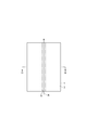
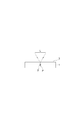
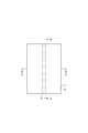
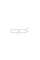
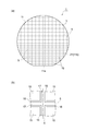
- FIG. 3 is a cross-sectional view taken along the line III-III of the workpiece in FIG. 2. It is a top view of the processing target after laser processing.
- FIG. 5 is a cross-sectional view taken along the line VV of the workpiece in FIG. 4.
- FIG. 5 is a cross-sectional view taken along line VI-VI of the workpiece in FIG. 4.
- the modified region is formed in the processing object along the planned cutting line by condensing the laser beam on the processing object.
- the formation of the modified region will be described with reference to FIGS.
- a laser processing apparatus 100 includes a laser light source 101 that oscillates a laser beam L, a dichroic mirror 103 that is arranged to change the direction of the optical axis (optical path) of the laser beam L by 90 °, and And a condensing lens 105 for condensing the laser light L. Further, the laser processing apparatus 100 includes a support base 107 for supporting the workpiece 1 irradiated with the laser light L condensed by the condensing lens 105, and a stage 111 for moving the support base 107. , A laser light source control unit 102 for controlling the laser light source 101 to adjust the output, pulse width, pulse waveform, and the like of the laser light L, and a stage control unit 115 for controlling the movement of the stage 111.
- the laser light L emitted from the laser light source 101 has its optical axis changed by 90 ° by the dichroic mirror 103, and the inside of the processing object 1 placed on the support base 107.
- the light is condensed by the condensing lens 105.
- the stage 111 is moved, and the workpiece 1 is moved relative to the laser beam L along the planned cutting line 5. Thereby, a modified region along the planned cutting line 5 is formed on the workpiece 1.
- the stage 111 is moved in order to move the laser light L relatively, but the condensing lens 105 may be moved, or both of them may be moved.
- a plate-like member for example, a substrate, a wafer, or the like
- a scheduled cutting line 5 for cutting the workpiece 1 is set in the workpiece 1.
- the planned cutting line 5 is a virtual line extending linearly.
- the laser beam L is cut in a state where the condensing point (condensing position) P is aligned with the inside of the workpiece 1 as shown in FIG. 3. It moves relatively along the planned line 5 (that is, in the direction of arrow A in FIG. 2).
- the modified region 7 is formed inside the workpiece 1 along the planned cutting line 5, and the modified region formed along the planned cutting line 5 is formed.
- the mass region 7 becomes the cutting start region 8.
- the condensing point P is a location where the laser light L is condensed.
- the planned cutting line 5 is not limited to a straight line, but may be a curved line, a three-dimensional shape in which these lines are combined, or a coordinate designated. Further, the planned cutting line 5 is not limited to a virtual line but may be a line actually drawn on the surface 3 of the workpiece 1.
- the modified region 7 may be formed continuously or intermittently. Further, the modified region 7 may be in the form of a line or a dot. In short, the modified region 7 only needs to be formed at least inside the workpiece 1.
- a crack may be formed starting from the modified region 7, and the crack and the modified region 7 may be exposed on the outer surface (front surface 3, back surface 21, or outer peripheral surface) of the workpiece 1.
- the laser light incident surface when forming the modified region 7 is not limited to the front surface 3 of the workpiece 1 but may be the back surface 21 of the workpiece 1.
- the laser beam L here passes through the workpiece 1 and is particularly absorbed in the vicinity of the condensing point P inside the workpiece 1, thereby forming the modified region 7 in the workpiece 1. (Ie, internal absorption laser processing). Therefore, since the laser beam L is hardly absorbed by the surface 3 of the workpiece 1, the surface 3 of the workpiece 1 is not melted. In general, when a removed portion such as a hole or a groove is formed by being melted and removed from the front surface 3 (surface absorption laser processing), the processing region gradually proceeds from the front surface 3 side to the back surface side.
- the modified region 7 formed in the present embodiment refers to a region in which the density, refractive index, mechanical strength, and other physical characteristics are different from the surroundings.
- the modified region 7 include a melt treatment region (meaning at least one of a region once solidified after melting, a region in a molten state, and a region in a state of being resolidified from melting), a crack region, and the like.
- a melt treatment region meaning at least one of a region once solidified after melting, a region in a molten state, and a region in a state of being resolidified from melting
- a crack region and the like.
- there are a dielectric breakdown region, a refractive index change region, and the like there is a region in which these are mixed.
- the modified region 7 includes a region in which the density of the modified region 7 is changed in comparison with the density of the non-modified region in the material of the workpiece 1 and a region in which lattice defects are formed (these are Collectively referred to as the high-density transition region).
- the melt-processed region, the refractive index changing region, the region where the density of the modified region 7 is changed compared with the density of the non-modified region, and the region where lattice defects are formed further
- cracks are included in the interface between the region 7 and the non-modified region.
- the included crack may be formed over the entire surface of the modified region 7, or may be formed in only a part or a plurality of parts.
- Examples of the processing object 1 include those containing or consisting of silicon (Si), glass, silicon carbide (SiC), LiTaO 3 or sapphire (Al 2 O 3 ).
- the modified region 7 is formed by forming a plurality of modified spots (processing marks) along the planned cutting line 5.
- the modified spot is a modified portion formed by one pulse shot of pulsed laser light (that is, one pulse of laser irradiation: laser shot).
- Examples of the modified spot include a crack spot, a melting treatment spot, a refractive index change spot, or a mixture of at least one of these.
- the size of the modified spot and the length of the crack to be generated are determined. It can be appropriately controlled.
- the laser processing apparatus 300 includes a laser light source 202, a reflective spatial light modulator (aberration adjustment unit) 203, a 4f optical system 241 and a condensing optical system 204 in a housing 231. .
- the laser processing apparatus 300 focuses the laser beam L on the workpiece 1 to form the modified region 7 on the workpiece 1 along the planned cutting line 5.
- the laser light source 202 emits laser light L having a wavelength of, for example, 1000 nm to 1500 nm, and is, for example, a fiber laser.
- the laser light source 202 here is fixed to the top plate 236 of the housing 231 with screws or the like so as to emit the laser light L in the horizontal direction.
- the reflective spatial light modulator 203 modulates the laser light L emitted from the laser light source 202, for example, a reflective liquid crystal (LCOS: Liquid Crystal on Silicon) spatial light modulator (SLM: Spatial Light Modulator). It is.
- the reflective spatial light modulator 203 modulates the laser beam L incident from the horizontal direction and reflects the laser beam L obliquely upward with respect to the horizontal direction.
- the reflective spatial light modulator 203 includes a silicon substrate 213, a drive circuit layer 914, a plurality of pixel electrodes 214, a reflective film 215 such as a dielectric multilayer mirror, an alignment film 999a, and a liquid crystal layer 216.
- An alignment film 999b, a transparent conductive film 217, and a transparent substrate 218 such as a glass substrate are stacked in this order.
- the transparent substrate 218 has a surface 218 a along the XY plane, and the surface 218 a constitutes the surface of the reflective spatial light modulator 203.
- the transparent substrate 218 is made of a light transmissive material such as glass, for example, and transmits the laser light L having a predetermined wavelength incident from the surface 218 a of the reflective spatial light modulator 203 into the reflective spatial light modulator 203.
- the transparent conductive film 217 is formed on the back surface of the transparent substrate 218 and is made of a conductive material (for example, ITO) that transmits the laser light L.
- the plurality of pixel electrodes 214 are arranged in a matrix on the silicon substrate 213 along the transparent conductive film 217.
- Each pixel electrode 214 is made of a metal material such as aluminum, for example, and the surface 214a is processed flat and smoothly.
- the plurality of pixel electrodes 214 are driven by an active matrix circuit provided in the drive circuit layer 914.
- the active matrix circuit is provided between the plurality of pixel electrodes 214 and the silicon substrate 213, and applies an applied voltage to each pixel electrode 214 according to the light image to be output from the reflective spatial light modulator 203.
- Control Such an active matrix circuit includes, for example, a first driver circuit that controls the applied voltage of each pixel column arranged in the X-axis direction (not shown) and a second driver circuit that controls the applied voltage of each pixel column arranged in the Y-axis direction.
- the driver circuit is configured so that a predetermined voltage is applied to the pixel electrode 214 of the pixel designated by both driver circuits by the control unit 250 (see FIG. 7).
- the alignment films 999a and 999b are disposed on both end faces of the liquid crystal layer 216, and align liquid crystal molecule groups in a certain direction.
- the alignment films 999a and 999b are made of, for example, a polymer material such as polyimide, and a contact surface with the liquid crystal layer 216 is subjected to a rubbing process or the like.
- the liquid crystal layer 216 is disposed between the plurality of pixel electrodes 214 and the transparent conductive film 217, and modulates the laser light L in accordance with an electric field formed by each pixel electrode 214 and the transparent conductive film 217. That is, when a voltage is applied to each pixel electrode 214 by the active matrix circuit of the drive circuit layer 914, an electric field is formed between the transparent conductive film 217 and each pixel electrode 214, and the electric field formed in the liquid crystal layer 216.
- the alignment direction of the liquid crystal molecules 216a changes depending on the size of the liquid crystal molecules.
- the laser light L passes through the transparent substrate 218 and the transparent conductive film 217 and enters the liquid crystal layer 216, the laser light L is modulated by the liquid crystal molecules 216 a while passing through the liquid crystal layer 216, and is reflected on the reflective film 215. After the reflection, the light is again modulated by the liquid crystal layer 216 and emitted.
- each pixel electrode 214 is controlled by the control unit 250 (see FIG. 7), and a portion sandwiched between the transparent conductive film 217 and each pixel electrode 214 in the liquid crystal layer 216 according to the voltage.
- the refractive index of the liquid crystal layer 216 at the position corresponding to each pixel changes.
- the phase of the laser light L can be changed for each pixel of the liquid crystal layer 216 in accordance with the applied voltage. That is, phase modulation corresponding to the hologram pattern can be applied to each pixel by the liquid crystal layer 216 (that is, the modulation pattern as the hologram pattern to be modulated is displayed on the liquid crystal layer 216 of the reflective spatial light modulator 203).
- the wavefront of the laser light L that enters and passes through the modulation pattern is adjusted, and the phase of the component in a predetermined direction orthogonal to the traveling direction is shifted in each light beam constituting the laser light L. Therefore, by appropriately setting the modulation pattern to be displayed on the reflective spatial light modulator 203, the laser light L can be modulated (for example, the intensity, amplitude, phase, polarization, etc. of the laser light L can be modulated).
- the 4f optical system 241 adjusts the wavefront shape of the laser light L modulated by the reflective spatial light modulator 203, and includes a first lens 241a and a second lens 241b.
- the distance between the reflective spatial light modulator 203 and the first lens 241a is the focal length f1 of the first lens 241a
- the distance between the condensing optical system 204 and the lens 241b is the focal length of the lens 241b.
- the reflective spatial light modulator 203 and the collector are set so that the distance between the first lens 241a and the second lens 241b is f1 + f2 and the first lens 241a and the second lens 241b are both-side telecentric optical systems. It is arranged between the optical optical system 204. According to the 4f optical system 241, it is possible to suppress the laser beam L modulated by the reflective spatial light modulator 203 from changing its wavefront shape due to spatial propagation and increasing aberration.
- the condensing optical system 204 condenses the laser light L emitted from the laser light source 202 and modulated by the reflective spatial light modulator 203 inside the workpiece 1.
- the condensing optical system 204 includes a plurality of lenses and is installed on the bottom plate 233 of the housing 231 via a drive unit 232 including a piezoelectric element and the like.
- the laser light L emitted from the laser light source 202 travels in the horizontal direction in the housing 231, is then reflected downward by the mirror 205 a, and is reflected by the attenuator 207. Strength is adjusted. Then, the light is reflected in the horizontal direction by the mirror 205 b, the intensity distribution of the laser light L is made uniform by the beam homogenizer 260, and is incident on the reflective spatial light modulator 203.
- the laser beam L incident on the reflective spatial light modulator 203 is modulated in accordance with the modulation pattern transmitted through the modulation pattern displayed on the liquid crystal layer 216, and then reflected upward by the mirror 206a.
- the polarization direction is changed by the two-wavelength plate 228, reflected in the horizontal direction by the mirror 206b, and enters the 4f optical system 241.
- the wavefront shape of the laser light L incident on the 4f optical system 241 is adjusted so as to be incident on the condensing optical system 204 as parallel light. Specifically, the laser light L is transmitted and converged through the first lens 241a, reflected downward by the mirror 219, diverged through the confocal O, and transmitted through the second lens 241b to become parallel light. Will converge again. Then, the laser light L sequentially passes through the dichroic mirrors 210 and 238 and enters the condensing optical system 204, and is condensed by the condensing optical system 204 in the workpiece 1 placed on the stage 111. .
- the laser processing apparatus 300 also includes a surface observation unit 211 for observing the laser light incident surface of the workpiece 1 and an AF (AutoFocus) for finely adjusting the distance between the condensing optical system 204 and the workpiece 1. ) Unit 212 and housing 231.
- the surface observation unit 211 includes an observation light source 211a that emits visible light VL1, and a detector 211b that receives and detects the reflected light VL2 of the visible light VL1 reflected by the laser light incident surface of the workpiece 1.
- the visible light VL 1 emitted from the observation light source 211 a is reflected and transmitted by the mirror 208 and the dichroic mirrors 209, 210, and 238, and condensed toward the workpiece 1 by the condensing optical system 204. Is done.
- the reflected light VL2 reflected by the laser light incident surface of the workpiece 1 is condensed by the condensing optical system 204, transmitted and reflected by the dichroic mirrors 238 and 210, and then transmitted through the dichroic mirror 209.
- Light is received by the detector 211b.
- the AF unit 212 emits the AF laser light LB1, receives and detects the reflected light LB2 of the AF laser light LB1 reflected by the laser light incident surface, thereby detecting the laser light incident surface along the planned cutting line 5 Get the displacement data. Then, when forming the modified region 7, the AF unit 212 drives the drive unit 232 based on the acquired displacement data, and moves the condensing optical system 204 in the optical axis direction so as to follow the undulation of the laser light incident surface. Move back and forth.
- the laser processing apparatus 300 includes a control unit 250 including a CPU, a ROM, a RAM, and the like as a unit for controlling the laser processing apparatus 300.
- the control unit 250 controls the laser light source 202 and adjusts the output, pulse width, and the like of the laser light L emitted from the laser light source 202. Further, when the control unit 250 forms the modified region 7, the condensing point P of the laser light L is located at a predetermined distance from the front surface 3 or the back surface 21 of the workpiece 1 and the condensing point P of the laser light L is present. Controls at least one of the housing 231, the position of the stage 111, and the drive of the drive unit 232 so as to relatively move along the scheduled cutting line 5.
- the control unit 250 applies a predetermined voltage to each pixel electrode 214 in the reflective spatial light modulator 203 to display a predetermined modulation pattern on the liquid crystal layer 216, thereby The laser beam L is modulated as desired by the reflective spatial light modulator 203.
- the modulation pattern displayed on the liquid crystal layer 216 includes, for example, the position where the modified region 7 is to be formed, the wavelength of the laser light L to be irradiated, the material of the workpiece 1, the condensing optical system 204, and the processing It is derived in advance based on the refractive index of the object 1 and stored in the control unit 250.
- This modulation pattern includes an individual difference correction pattern for correcting individual differences generated in the laser processing apparatus 300 (for example, distortion generated in the liquid crystal layer 216 of the reflective spatial light modulator 203), and spherical aberration for correcting spherical aberration.
- a correction pattern and the like are included.
- the control unit 250 and the reflective spatial light modulator 203 function as an aberration adjusting unit that adjusts the aberration generated at the condensing position due to the condensing of the laser light L on the workpiece 1. .
- a workpiece 1 to be processed by the laser processing apparatus 300 configured as described above includes a substrate 11 made of, for example, silicon and a surface 11 a of the substrate 11. And a plurality of functional elements 15 formed on the substrate.
- the plurality of functional elements 15 are arranged in a matrix on the surface 11 a of the substrate 11 and include wirings 16.
- the workpiece 1 is provided with a plurality of functional elements 15 including the wiring 16 on the surface (first surface) 3 thereof.
- the functional element 15 is a light receiving element such as a photodiode, a light emitting element such as a laser diode, or a circuit element formed as a circuit.
- the laser processing method implemented in the laser processing apparatus 300 is used as a chip manufacturing method for manufacturing a plurality of chips by cutting the workpiece 1 for each functional element 15. Therefore, in the laser processing method, the processing object 1 passes through the street region (area) 17 between the adjacent functional elements 15 (when viewed from the thickness direction of the processing object 1, the street A plurality of cutting lines 5 are set in a lattice shape (through the center of the width of the region 17). Then, the laser beam L incident from the back surface (second surface) 21 of the workpiece 1 that is the back surface 11 b of the substrate 11 is focused on the workpiece 1 and is processed along each scheduled cutting line 5. 1, the modified region 7 is formed.
- the laser processing method performed in the laser processing apparatus 300 will be described from the background.
- the optical axis of the laser beam L is caused by spherical aberration.
- the condensing region region where each light beam constituting the laser beam L is condensed
- the laser light L is condensed. Condensed at point P.
- the laser beam L extends from the modified region to the incident side of the laser beam L and the opposite side when the modified region is formed.
- the length of the crack is longer when the aberration is corrected than when the aberration is not corrected.
- the increase in the length of the cracks can reduce the number of columns of the modified regions to be formed for one cutting scheduled line 5 in order to cut the workpiece 1. This is advantageous for shortening.
- the laser beam L was irradiated under the conditions of a frequency of 80 kHz, a pulse width of 500 ns, an exit output of 1.2 W, and a scanning speed (relative moving speed of the condensing point along the planned cutting line 5) of 300 mm / s.
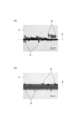
- the damage D occurred in a region exceeding the width of the laser beam L (the region outside the width of the leaked light). From this, it is considered that the laser beam L is not a cause of damage D.
- the lower stage of FIG. 12 is a plane photograph of the workpiece 1.
- the back surface of the silicon substrate is the laser light incident surface, and the focal point of the laser light is aligned with the surface of the silicon substrate (that is, near the interface between the silicon substrate and the Au film).
- the laser beam L was irradiated under the conditions of a frequency of 90 kHz, a pulse width of 90 ns, an exit output of 1.27 W, and a scanning speed of 340 mm / s.
- the workpiece 1 in which no cracks are formed in advance along the scheduled cutting line 5 and the planned cutting line 5 is prepared in advance along the cutting line 5 without correcting the aberration generated at the condensing position of the laser beam L.
- Laser light L was irradiated.
- the workpiece 1 is preliminarily formed in comparison with the case where no crack is formed in the workpiece 1 in advance. More damage D occurred when cracks were formed.
- this one-pulse laser irradiation overlaps the modified region formed by the previous one-pulse laser irradiation or a crack extended from the modified region, the current one-pulse laser irradiation ,
- the modified region formed by the previous one-pulse laser irradiation or a crack extending from the modified region acts like a mirror surface, and a part of the laser light L of the current one-pulse laser irradiation is reflected, Interference, diffraction, scattering, etc.
- Reflection, interference, diffraction, scattering, etc. occur for a part of the laser beam L of the pulsed laser irradiation, and a part of the laser beam L is irradiated to a region exceeding the width of the laser beam L, As a result, part of the laser light L is absorbed by the wiring 16 of the functional element 15 and the melting occurs in the wiring 16 and the like.
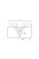
- a position shifted from the condensing position CP1 along the optical axis of the laser light L to the incident side of the laser light L by a predetermined distance is determined as a reference aberration.
- the light is condensed at the condensing position CP1 with an aberration correction amount in a state where the ideal condensing position CP0 is shifted by a predetermined distance from the condensing position CP1 along the optical axis of the laser light L to the incident side of the laser light L.
- the aberration that occurs in this case is determined as the reference aberration.
- This reference aberration is set in the control unit 250.
- the condensing position CP1 is a position where the formation of the modified region is planned, and corresponds to, for example, the position of the end of the modified region scheduled to be formed on the side opposite to the incident side of the laser beam L. .
- the ideal condensing position CP0 is the position of the condensing point of the laser light L that has undergone ideal condensing (that is, a condensing state in which aberrations are reduced to near the condensing state when it is assumed that there is no medium). It is.
- the aberration generated at the condensing position CP1 is adjusted so that the first condensing length is longer than the reference condensing length of the reference aberration and the first condensing intensity is weaker than the reference condensing intensity of the reference aberration.
- the reference condensing length of the reference aberration is adjusted so that the second condensing length is shorter than the first condensing length and the second condensing intensity is stronger than the reference condensing intensity of the reference aberration. Adjustment of these aberrations is performed by the control unit 250 and the reflective spatial light modulator 203.
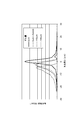
- the light collection length is the length of a light collection region (region where each light beam constituting the laser light L is collected) along the optical axis of the laser light L. Further, the light collection intensity is the intensity of the laser light per unit area in the light collection region.
- the above-mentioned reference aberration was examined by experiment.
- the experimental conditions are as follows. 1. A silicon substrate having a workpiece (1) thickness of 250 ⁇ m, a crystal orientation (100), and a resistance value of 1 ⁇ ⁇ cm was prepared. 2. Laser light irradiation conditions (1) The condensing position CP1 and the ideal condensing position CP0 in the laser light L are adjusted under the conditions shown in Table 1 below, the wavelength is 1080 nm, the repetition frequency is 80 kHz, the pulse width is 500 ns, the exit power is 1.2 W, The laser beam L was irradiated at a scanning speed of 300 mm / s.
- the “front surface” is the surface 3 of the workpiece 1 on the side opposite to the incident side of the laser beam L
- the “back surface” is the workpiece 1 on the incident side of the laser beam L. It is the back surface 21.
- the “deviation amount” is a position from a light collecting position (that is, a position where light is condensed to form a modified region) to an ideal light collecting position (that is, a light collecting position where the light is condensed by aberration correction).
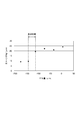
- FIGS. 16 and 17 As a result of this experiment, as shown in FIGS. 16 and 17, when the ideal condensing position CP0 is shifted to the incident side of the laser beam L, if the absolute value of the shift amount becomes smaller than 110 ⁇ m, the damage D It has been found that the width of the damage D becomes smaller when the width becomes larger and the absolute value of the shift amount becomes larger than 140 ⁇ m.
- FIG. 17 is a plane photograph of the workpiece 1, and each of No. 1 in Table 1 is shown. 1-No. It is a result in the case of 6.
- the absolute value of the deviation amount is 110 ⁇ m or more and 140 ⁇ m or less. May be determined as the reference aberration.
- the modified region is formed in the first region closest to the surface 3 of the workpiece 1 on the side opposite to the incident side of the laser light L, the first collection longer than the reference condensing length of the reference aberration.
- the modified region is formed in the second region closer to the back surface 21 of the workpiece 1 on the incident side of the laser light L than the first region, the second shift amount shorter than the reference shift amount of the reference aberration.
- the aberration generated at the condensing position CP1 may be adjusted.
- the experimental conditions are as follows. 1. A silicon substrate having a workpiece (1) thickness of 250 ⁇ m, a crystal orientation (100), and a resistance value of 1 ⁇ ⁇ cm was prepared. 2. Laser light irradiation conditions (1) The condensing position CP1 and the ideal condensing position CP0 in the laser light L are adjusted under the conditions shown in FIG. 19, and the wavelength is 1080 nm, the repetition frequency is 80 kHz, the pulse width is 500 ns, the exit output is 1.2 W, The laser beam L was irradiated at a scanning speed of 300 mm / s. In FIG.
- the “surface” is the surface 3 of the workpiece 1 on the side opposite to the incident side of the laser beam L.
- first processing condition means that the first light collection length is longer than the reference light collection length of the reference aberration and the first light collection intensity is weaker than the reference light collection intensity of the reference aberration. This is a condition in which the aberration generated at the optical position CP1 is adjusted.
- second processing condition is a second condensing length shorter than the reference condensing length of the reference aberration and is smaller than the reference condensing intensity of the reference aberration. This is a condition in which the aberration generated at the condensing position CP1 is adjusted so that the second condensing intensity is strong.
- FIG. 19 is a plane photograph of the workpiece 1.
- the first processing condition that is, the reference condensing of the reference aberration.
- the first condensing length is longer than the length and the first condensing intensity is weaker than the reference condensing intensity of the reference aberration, and the aberration generated at the condensing position CP1 is adjusted).
- One region may be set to a region whose distance from the surface 3 of the workpiece 1 is 60 ⁇ m or less.
- the second processing condition that is, the reference condensing of the reference aberration.
- the second condensing length is shorter than the length and the second condensing intensity is larger than the reference condensing intensity of the reference aberration. What is necessary is just to set 2 area
- the first condensing length is longer than the reference condensing length of the reference aberration, and Aberration is adjusted so that the first focused intensity is weaker than the reference focused intensity, and the laser beam L is focused on the workpiece 1 so that the workpiece on the side opposite to the incident side of the laser beam L is obtained.
- the modified region 7 is formed in the first region closest to the surface 3 of the object 1 (first step).
- the second light collection length is shorter than the reference light collection length of the reference aberration, and the second light collection intensity is stronger than the reference light collection intensity of the reference aberration.
- the modified region is in the second region closer to the back surface 21 of the workpiece 1 on the incident side of the laser beam L than the first region. 7 is formed (second step).
- a crack extending from the modified region 7 to the side opposite to the incident side of the laser beam L reaches the surface 3 of the workpiece 1. It is set not to.
- the second region is set so as not to overlap with a crack extending from the modified region 7 to the incident side of the laser beam L when the modified region 7 is formed in the first region.
- the laser beam L is incident on the incident side of the laser beam L along the optical axis of the laser beam L from the condensing position CP1 by a predetermined distance.
- the aberration generated at the condensing position CP1 in a state where the ideal condensing position CP0 is shifted is set as a reference aberration, and the first condensing length is longer than the reference condensing length of the reference aberration and is larger than the reference condensing intensity of the reference aberration.
- the surface 3 of the workpiece 1 on the side opposite to the incident side of the laser beam L is applied.
- the modified region 7 is formed in the nearest first region.
- the aberration is adjusted so that the second light collection length is shorter than the reference light collection length of the reference aberration and the second light collection intensity is higher than the reference light collection intensity of the reference aberration.
- the modified region 7 is formed in the second region closer to the back surface 21 of the workpiece 1 on the incident side of the laser beam L than the first region.
- a plurality of functional elements 15 including the wiring 16 are provided on the surface 3 of the workpiece 1, and the planned cutting line 5 is set so as to pass through the street region 17 between the adjacent functional elements 15. Yes. Thereby, it is possible to suppress the occurrence of damage D on the wiring 16 included in the functional element 15.
- the first region in which the aberration is adjusted so that the first condensing length is longer than the reference condensing length of the reference aberration and the first condensing intensity is weaker than the reference condensing intensity of the reference aberration is processed.
- the distance from the surface 3 of the object 1 is set to an area of 60 ⁇ m or less.
- a second region in which the aberration is adjusted so that the second light collection length is shorter than the reference light collection length of the reference aberration and the second light collection intensity is higher than the reference light collection intensity of the reference aberration is processed.
- the distance from the surface 3 of the object 1 is set to an area of 40 ⁇ m or more.
- the light is condensed at the condensing position CP1 with an aberration correction amount in a state where the ideal condensing position CP0 is shifted by a predetermined distance from the condensing position CP1 along the optical axis of the laser light L to the incident side of the laser light L.
- the predetermined distance is set to 110 ⁇ m or more and 140 ⁇ m or less. Thereby, the reference aberration can be set appropriately.
- the modified region 7 when the modified region 7 is formed in the first region, the cracks extending from the modified region 7 to the side opposite to the incident side of the laser beam L do not reach the surface 3 of the workpiece 1.
- One area is set.
- the second region is set so as not to overlap with the crack extending from the modified region 7 to the incident side of the laser beam L. Accordingly, when the modified region 7 is formed in the second region, the formed crack is prevented from acting like a mirror surface, so that the surface 3 of the workpiece 1 is out of the planned cutting line 5. It can suppress more reliably that the damage D generate
- the reference The aberration can be adjusted so that the first condensing length is longer than the reference condensing length of the aberration and the first condensing intensity is weaker than the reference condensing intensity of the reference aberration.
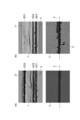
- FIG. 22 is a diagram showing a comparison between the result of the example using the spherical aberration correction pattern and the result of the comparative example not using the spherical aberration correction pattern.
- 22A is a cross-sectional photograph of the workpiece 1 according to the embodiment, and the lower row of FIG. 22A is a plane photograph of the workpiece 1 according to the embodiment.
- the upper stage of FIG.22 (b) is a cross-sectional photograph of the workpiece 1 by a comparative example, and the lower stage of FIG.22 (b) is a plane photograph of the workpiece 1 by a comparative example.
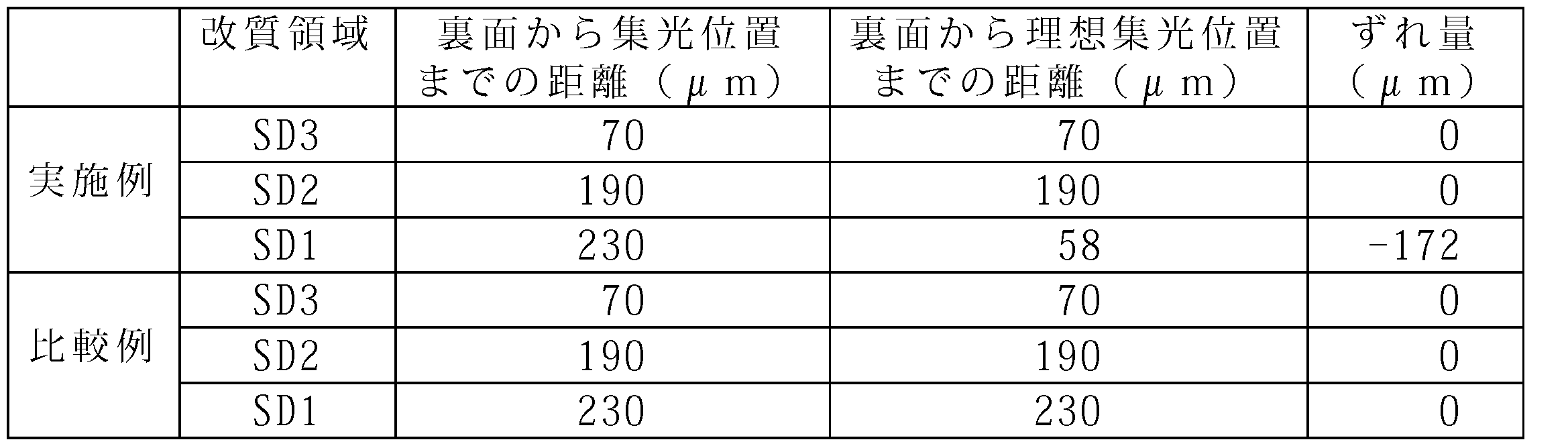
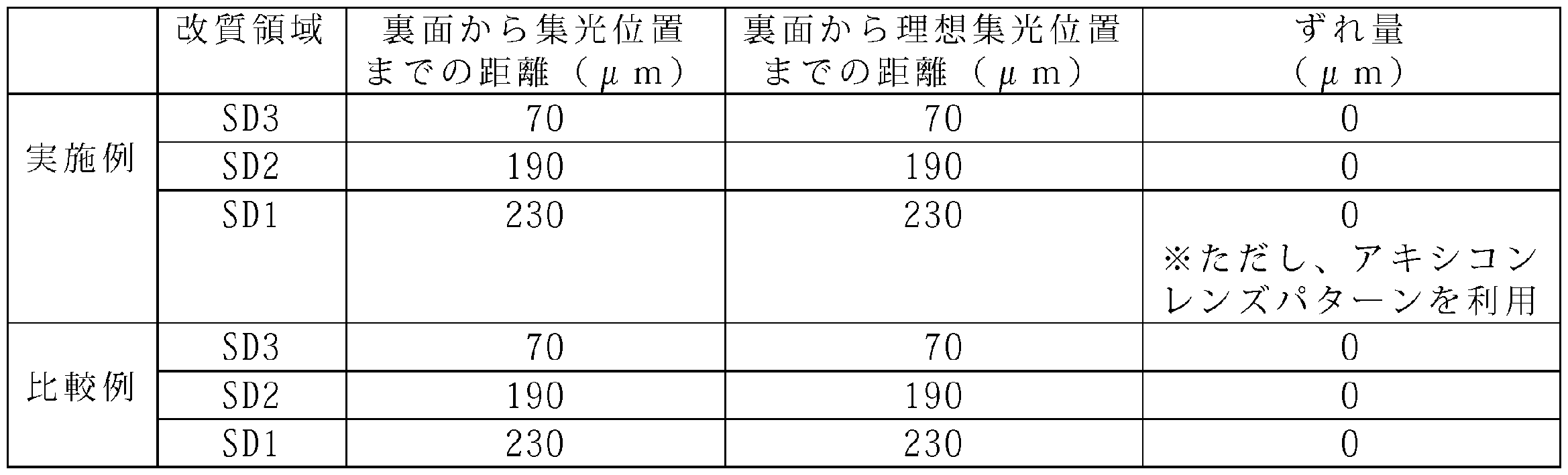
- the experimental conditions are as follows. 1. Workpiece (1) A silicon substrate having a thickness of 250 ⁇ m was prepared. 2.
- the condensing position CP1 and the ideal condensing position CP0 in the laser light L are adjusted under the conditions shown in Table 2 below, the wavelength is 1080 nm, the repetition frequency is 92 kHz, the pulse width is 500 ns, the processing energy is 15 ⁇ J, The laser beam L was irradiated at a scanning speed of 345 mm / s.
- “back surface” is the back surface 21 of the workpiece 1 on the incident side of the laser beam L.
- the “deviation amount” is a distance from the condensing position to the ideal condensing position, and the case where the ideal condensing position CP0 is deviated to the incident side of the laser beam L with respect to the condensing position CP1.
- the case where the ideal condensing position CP0 is shifted to the side opposite to the incident side of the laser beam L is represented by the value “+”.
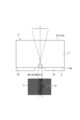
- FIG. 23 is a diagram showing a comparison between the result of the example using the axicon lens pattern and the result of the comparative example not using the axicon lens pattern.
- 23A is a cross-sectional photograph of the workpiece 1 according to the embodiment
- the lower row of FIG. 23A is a plan photograph of the workpiece 1 according to the embodiment.
- the upper stage of FIG.23 (b) is a cross-sectional photograph of the workpiece 1 by a comparative example
- the lower stage of FIG.23 (b) is a plane photograph of the workpiece 1 by a comparative example.
- the experimental conditions are as follows. 1. Workpiece (1) A silicon substrate having a thickness of 250 ⁇ m was prepared. 2.
- the condensing position CP1 and the ideal condensing position CP0 in the laser light L are adjusted under the conditions shown in Table 3 below, the wavelength is 1080 nm, the repetition frequency is 92 kHz, the pulse width is 500 ns, the processing energy is 15 ⁇ J, The laser beam L was irradiated at a scanning speed of 345 mm / s.
- the “back surface” is the back surface 21 of the workpiece 1 on the incident side of the laser beam L.
- the “deviation amount” is a distance from the light collecting position to the ideal light collecting position.
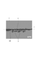
- FIG. 24 is a diagram illustrating a result of a reference example in which energy is adjusted, and is a cross-sectional photograph of the workpiece 1.
- the experimental conditions are as follows. 1. Workpiece (1) A silicon substrate having a thickness of 300 ⁇ m was prepared. 2. Laser light irradiation conditions (1) The condensing position CP1 and the ideal condensing position CP0 and the processing energy in the laser light L are adjusted under the conditions shown in Table 4 below, the wavelength is 1342 nm, the repetition frequency is 60 kHz, the pulse width is 60 ns, and the scan The laser beam L was irradiated at a speed of 340 mm / s. In Table 4, the “back surface” is the back surface 21 of the workpiece 1 on the incident side of the laser beam L. The “deviation amount” is a distance from the light collecting position to the ideal light collecting position.
- the processing energy for forming the modified region 7 in the first region (the first region closest to the surface 3 of the workpiece 1 on the side opposite to the incident side of the laser beam L) is the second region ( Compared to the processing energy for forming the modified region 7 in the second region closer to the back surface 21 of the workpiece 1 on the incident side of the laser light L than the first region).
- the processing energy for forming the modified region 7 in the first region is 10 ⁇ m or less.
- Black streaks are formed between the modified region 7 formed in the first region and the modified region 7 formed in the second region (see FIG.
- the modified region 7 formed in the first region and the modified region 7 formed in the second region are separated by 60 ⁇ m or more. (5) When the modified region 7 is formed in the first region, the crack extending from the modified region 7 does not reach the surface 3 of the workpiece 1 and the modified region 7 is formed in the second region. In this case, the crack reaches the surface 3 of the workpiece 1.
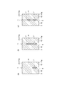
- the modified region 7 is formed in the first region along the planned cutting line 5, and then, along the planned cutting line 5 as shown in FIG. 25 (b).
- the crack extended from the modified region 7 formed along the thickness direction of the workpiece 1 may reach the front surface 3 and the back surface 21 of the workpiece 1.
- the crack extended from the modified region formed in the first region and the crack extended from the modified region formed in the second region are connected.
- the crack extended from the modified region 7 in the thickness direction of the workpiece 1 is processed while the modified region 7 is formed in the second region and before the expanded tape is expanded. May reach the front surface 3 and the back surface 21.
- the modified region 7 is formed in the first region along the planned cutting line 5, and then, as shown in FIG. Then, the modified region 7 is formed in the second region, and then, the expanded tape attached to the back surface 21 of the workpiece 1 is expanded, so that the line to be cut is formed as shown in FIG. 5 may be caused to reach the front surface 3 and the back surface 21 of the workpiece 1 from the modified region 7 formed along the thickness 5 of the workpiece 1.
- the crack extended from the modified region formed in the first region is connected to the crack extended from the modified region formed in the second region. ing.
- the crack extended from the modified region 7 in the thickness direction of the workpiece 1 is processed while the modified region 7 is formed in the second region and before the expanded tape is expanded. May reach the front surface 3 and the back surface 21.
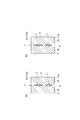
- the laser light L is condensed into the first region and the second region at the same time, and along the planned cutting line 5 as shown in FIG.
- the modified region 7 is formed simultaneously in the first region and the second region, and then the expanded tape attached to the back surface 21 of the workpiece 1 is expanded.
- the cracks extending in the thickness direction of the workpiece 1 from the modified region 7 formed along the planned cutting line 5 may reach the front surface 3 and the back surface 21 of the workpiece 1.
- the crack extends from the modified region formed in the first region, and extends from the modified region formed in the second region. The crack is not connected.
- the crack extended from the modified region 7 in the thickness direction of the workpiece 1 is from the middle of forming the modified region 7 in the first region and the second region to before expanding the expanded tape.
- the front surface 3 and the back surface 21 of the workpiece 1 may be reached.
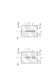
- the laser light L is condensed into the first region and the second region at the same time, and along the planned cutting line 5 as shown in FIG.
- the modified region 7 is simultaneously formed in the first region and the second region, and then the expanded tape attached to the back surface 21 of the workpiece 1 is expanded.
- the cracks extending in the thickness direction of the workpiece 1 from the modified region 7 formed along the planned cutting line 5 may reach the front surface 3 and the back surface 21 of the workpiece 1.
- the crack extended from the modified region 7 in the thickness direction of the workpiece 1 is from the middle of forming the modified region 7 in the first region and the second region to before expanding the expanded tape.
- the front surface 3 and the back surface 21 of the workpiece 1 may be reached.
- this invention is not limited to the said embodiment.
- the distance from the surface 3 of the workpiece on the side opposite to the incident side of the laser beam L is predetermined.
- the modified region 7 is formed in the first region that is equal to or less than the distance, the first light collection intensity that is longer than the reference light collection length of the reference aberration and is weaker than the reference light collection intensity of the reference aberration If the aberration is adjusted so as to be, damage D can be prevented from occurring in a part of the surface 3 of the workpiece 1 that is off the planned cutting line 5.
- the substrate 11 may be a semiconductor substrate other than a silicon substrate, a sapphire substrate, a SiC substrate, a glass substrate (tempered glass substrate), a transparent insulating substrate, or the like.
- the laser processing apparatus and laser processing method which can suppress that damage generate
- DESCRIPTION OF SYMBOLS 1 ... Processing target object, 3 ... Surface (1st surface), 5 ... Planned cutting line, 7 ... Modified area
Landscapes
- Physics & Mathematics (AREA)
- Optics & Photonics (AREA)
- Engineering & Computer Science (AREA)
- Plasma & Fusion (AREA)
- Mechanical Engineering (AREA)
- Chemical & Material Sciences (AREA)
- Materials Engineering (AREA)
- Organic Chemistry (AREA)
- Chemical Kinetics & Catalysis (AREA)
- General Chemical & Material Sciences (AREA)
- Oil, Petroleum & Natural Gas (AREA)
- Laser Beam Processing (AREA)
- Dicing (AREA)
Abstract
Description
1.加工対象物
(1)厚さ250μm、結晶方位(100)のシリコン基板の表面に、厚さ300ÅのAu膜を形成した。
(2)(a)では、切断予定ライン5を覆うようにAu膜を形成し、(b)では、切断予定ライン5に沿って幅15μmのストリート領域が形成されるようにAu膜を形成した。
2.レーザ光の照射条件
(1)シリコン基板の裏面をレーザ光入射面として、レーザ光の集光点をシリコン基板の表面(すなわち、シリコン基板とAu膜との界面近傍)に合せ、波長1080nm、繰り返し周波数80kHz、パルス幅500ns、出口出力1.2W、スキャン速度(切断予定ライン5に沿っての集光点の相対的移動速度)300mm/sの条件でレーザ光Lを照射した。
1.加工対象物
(1)厚さ250μm、結晶方位(100)、抵抗値1Ω・cmのシリコン基板の表面に、厚さ300ÅのAu膜を形成した。
(2)切断予定ライン5を覆うようにAu膜を形成した。
2.レーザ光の照射条件
(1)シリコン基板の裏面をレーザ光入射面として、レーザ光の集光点をシリコン基板の表面(すなわち、シリコン基板とAu膜との界面近傍)に合せ、波長1342nm、繰り返し周波数90kHz、パルス幅90ns、出口出力1.27W、スキャン速度340mm/sの条件でレーザ光Lを照射した。
1.1本の切断予定ライン5に沿って1列の改質領域を形成した後に、当該1本の切断予定ライン5に沿って他の1列の改質領域を形成する場合に、形成済みの1列の改質領域又は当該改質領域から伸展した亀裂に、レーザ光Lの集光位置が重なっていると、レーザ光Lの照射時に、形成済みの1列の改質領域又は当該改質領域から伸展した亀裂が鏡面のように作用し、レーザ光Lの一部について、反射、干渉、回折、散乱等が起こって、当該レーザ光Lの一部が、レーザ光Lの抜け光の幅を超える領域に照射され、その結果、当該レーザ光Lの一部が機能素子15の配線16等で吸収されて、配線16等に溶融が発生する。
2.前回の1パルスのレーザ照射で形成された改質領域又は当該改質領域から伸展した亀裂に、今回の1パルスのレーザ照射の集光位置が重なっていると、今回の1パルスのレーザ照射時に、前回の1パルスのレーザ照射で形成された改質領域又は当該改質領域から伸展した亀裂が鏡面のように作用し、今回の1パルスのレーザ照射のレーザ光Lの一部について、反射、干渉、回折、散乱等が起こって、当該レーザ光Lの一部が、レーザ光Lの抜け光の幅を超える領域に照射され、その結果、当該レーザ光Lの一部が機能素子15の配線16等で吸収されて、配線16等に溶融が発生する。
3.前回の1パルスのレーザ照射で形成された改質領域から伸展した亀裂が加工対象物1の表面3又は裏面21に到達した状態で、当該亀裂に集光位置が重なるように、今回の1パルスのレーザ照射が行われると、今回の1パルスのレーザ照射時に、前回の1パルスのレーザ照射で加工対象物1の表面3又は裏面21に到達した亀裂が鏡面のように作用し、今回の1パルスのレーザ照射のレーザ光Lの一部について、反射、干渉、回折、散乱等が起こって、当該レーザ光Lの一部が、レーザ光Lの抜け光の幅を超える領域に照射され、その結果、当該レーザ光Lの一部が機能素子15の配線16等で吸収されて、配線16等に溶融が発生する。
1.加工対象物
(1)厚さ250μm、結晶方位(100)、抵抗値1Ω・cmのシリコン基板を準備した。
2.レーザ光の照射条件
(1)下記の表1の条件でレーザ光Lにおける集光位置CP1及び理想集光位置CP0を調整し、波長1080nm、繰り返し周波数80kHz、パルス幅500ns、出口出力1.2W、スキャン速度300mm/sの条件でレーザ光Lを照射した。なお、表1において、「表面」とは、レーザ光Lの入射側とは反対側の加工対象物1の表面3であり、「裏面」とは、レーザ光Lの入射側の加工対象物1の裏面21である。また、「ずれ量」とは、集光位置(すなわち、改質領域を形成するために集光したい位置)から理想集光位置(すなわち、収差補正により理想集光となる集光位置)までの距離であり、集光位置CP1を基準として、理想集光位置CP0がレーザ光Lの入射側にずれている場合を「-」の数値で表し、理想集光位置CP0がレーザ光Lの入射側とは反対側にずれている場合を「+」の数値で表した。

1.加工対象物
(1)厚さ250μm、結晶方位(100)、抵抗値1Ω・cmのシリコン基板を準備した。
2.レーザ光の照射条件
(1)図19に示される条件でレーザ光Lにおける集光位置CP1及び理想集光位置CP0を調整し、波長1080nm、繰り返し周波数80kHz、パルス幅500ns、出口出力1.2W、スキャン速度300mm/sの条件でレーザ光Lを照射した。なお、図19において、「表面」とは、レーザ光Lの入射側とは反対側の加工対象物1の表面3である。また、「第1加工条件」とは、基準収差の基準集光長さよりも長い第1集光長さとなり且つ基準収差の基準集光強度よりも弱い第1集光強度となるように、集光位置CP1で発生する収差を調整した条件であり、「第2加工条件」とは、基準収差の基準集光長さよりも短い第2集光長さとなり且つ基準収差の基準集光強度よりも強い第2集光強度となるように、集光位置CP1で発生する収差を調整した条件である。
1.加工対象物
(1)厚さ250μmのシリコン基板を準備した。
2.レーザ光の照射条件
(1)下記の表2に示される条件でレーザ光Lにおける集光位置CP1及び理想集光位置CP0を調整し、波長1080nm、繰り返し周波数92kHz、パルス幅500ns、加工エネルギー15μJ、スキャン速度345mm/sの条件でレーザ光Lを照射した。なお、表2において、「裏面」とは、レーザ光Lの入射側の加工対象物1の裏面21である。また、「ずれ量」とは、集光位置から理想集光位置までの距離であり、集光位置CP1を基準として、理想集光位置CP0がレーザ光Lの入射側にずれている場合を「-」の数値で表し、理想集光位置CP0がレーザ光Lの入射側とは反対側にずれている場合を「+」の数値で表した。
1.加工対象物
(1)厚さ250μmのシリコン基板を準備した。
2.レーザ光の照射条件
(1)下記の表3に示される条件でレーザ光Lにおける集光位置CP1及び理想集光位置CP0を調整し、波長1080nm、繰り返し周波数92kHz、パルス幅500ns、加工エネルギー15μJ、スキャン速度345mm/sの条件でレーザ光Lを照射した。なお、表3において、「裏面」とは、レーザ光Lの入射側の加工対象物1の裏面21である。また、「ずれ量」とは、集光位置から理想集光位置までの距離である。
1.加工対象物
(1)厚さ300μmのシリコン基板を準備した。
2.レーザ光の照射条件
(1)下記の表4に示される条件でレーザ光Lにおける集光位置CP1及び理想集光位置CP0並びに加工エネルギーを調整し、波長1342nm、繰り返し周波数60kHz、パルス幅60ns、スキャン速度340mm/sの条件でレーザ光Lを照射した。なお、表4において、「裏面」とは、レーザ光Lの入射側の加工対象物1の裏面21である。また、「ずれ量」とは、集光位置から理想集光位置までの距離である。

(1)第1領域(レーザ光Lの入射側とは反対側の加工対象物1の表面3に最も近い第1領域)に改質領域7を形成するための加工エネルギーを、第2領域(レーザ光Lの入射側の加工対象物1の裏面21に第1領域よりも近い第2領域)に改質領域7を形成するための加工エネルギーに比べ、小さくすること。
(2)第1領域に改質領域7を形成するための加工エネルギーを10μm以下にすること。
(3)第1領域に形成された改質領域7と第2領域に形成された改質領域7との間に黒筋が形成されること(図24参照)。
(4)第1領域に形成された改質領域7と第2領域に形成された改質領域7とが60μm以上離れること。
(5)第1領域に改質領域7を形成した際に、当該改質領域7から伸展した亀裂が加工対象物1の表面3に到達せず、第2領域に改質領域7を形成した際に、亀裂が加工対象物1の表面3に到達すること。
Claims (14)
- 加工対象物にレーザ光を集光することにより、切断予定ラインに沿って前記加工対象物に改質領域を形成するレーザ加工装置であって、
前記レーザ光を出射するレーザ光源と、
前記レーザ光源により出射された前記レーザ光を前記加工対象物に集光する集光光学系と、
前記加工対象物に前記レーザ光を集光することに起因して集光位置で発生する収差を調整する収差調整部と、を備え、
前記収差調整部は、
前記集光位置から前記レーザ光の光軸に沿って前記レーザ光の入射側に所定距離だけ理想集光位置をずらした状態での収差補正量で当該集光位置に集光した場合に発生する前記収差を基準収差として、
前記レーザ光の入射側とは反対側の前記加工対象物の第1表面に最も近い第1領域に前記改質領域を形成する場合には、前記基準収差の基準集光長さよりも長い第1集光長さとなり且つ前記基準収差の基準集光強度よりも弱い第1集光強度となるように前記収差を調整し、
前記レーザ光の入射側の前記加工対象物の第2表面に前記第1領域よりも近い第2領域に前記改質領域を形成する場合には、前記基準集光長さよりも短い第2集光長さとなり且つ前記基準集光強度よりも強い第2集光強度となるように前記収差を調整する、レーザ加工装置。 - 前記第1表面には、配線を含む複数の機能素子が設けられており、
前記切断予定ラインは、隣り合う前記機能素子の間の領域を通るように設定される、請求項1記載のレーザ加工装置。 - 前記第1領域は、前記第1表面からの距離が60μm以下の領域に設定される、請求項1又は2記載のレーザ加工装置。
- 前記第2領域は、前記第1表面からの距離が40μm以上の領域に設定される、請求項1又は2記載のレーザ加工装置。
- 前記所定距離は、110μm以上140μm以下である、請求項1~4のいずれか一項記載のレーザ加工装置。
- 加工対象物にレーザ光を集光することにより、切断予定ラインに沿って前記加工対象物に改質領域を形成するレーザ加工装置であって、
前記レーザ光を出射するレーザ光源と、
前記レーザ光源により出射された前記レーザ光を前記加工対象物に集光する集光光学系と、
前記加工対象物に前記レーザ光を集光することに起因して集光位置で発生する収差を調整する収差調整部と、を備え、
前記収差調整部は、
前記集光位置から前記レーザ光の光軸に沿って前記レーザ光の入射側に所定距離だけ理想集光位置をずらした状態での収差補正量で当該集光位置に集光した場合に発生する前記収差を基準収差として、
前記レーザ光の入射側とは反対側の前記加工対象物の第1表面からの距離が所定距離以下の第1領域に前記改質領域を形成する場合には、前記基準収差の基準集光長さよりも長い第1集光長さとなり且つ前記基準収差の基準集光強度よりも弱い第1集光強度となるように前記収差を調整する、レーザ加工装置。 - 加工対象物にレーザ光を集光することにより、切断予定ラインに沿って前記加工対象物に改質領域を形成するレーザ加工方法であって、
前記加工対象物に前記レーザ光を集光することに起因して集光位置で発生する収差を調整して、前記加工対象物に前記レーザ光を集光することにより、前記レーザ光の入射側とは反対側の前記加工対象物の第1表面に最も近い第1領域に前記改質領域を形成する第1工程と、
前記集光位置で発生する前記収差を調整して、前記加工対象物に前記レーザ光を集光することにより、前記レーザ光の入射側の前記加工対象物の第2表面に前記第1領域よりも近い第2領域に前記改質領域を形成する第2工程と、を含み、
前記第1工程においては、前記集光位置から前記レーザ光の光軸に沿って前記レーザ光の入射側に所定距離だけ理想集光位置をずらした状態での収差補正量で当該集光位置に集光した場合に発生する基準収差の基準集光長さよりも長い第1集光長さとなり且つ前記基準収差の基準集光強度よりも弱い第1集光強度となるように前記収差を調整し、
前記第2工程においては、前記基準集光長さよりも短い第2集光長さとなり且つ前記基準集光強度よりも強い第2集光強度となるように前記収差を調整する、レーザ加工方法。 - 前記第1表面には、配線を含む複数の機能素子が設けられており、
前記切断予定ラインは、隣り合う前記機能素子の間の領域を通るように設定される、請求項7記載のレーザ加工方法。 - 前記第1領域は、前記第1表面からの距離が60μm以下の領域に設定される、請求項7又は8記載のレーザ加工方法。
- 前記第2領域は、前記第1表面からの距離が40μm以上の領域に設定される、請求項7又は8記載のレーザ加工方法。
- 前記所定距離は、110μm以上140μm以下である、請求項7~10のいずれか一項記載のレーザ加工方法。
- 前記第1工程を実施した後に前記第2工程を実施する場合には、前記第1領域は、前記第1工程において前記改質領域から前記レーザ光の入射側とは反対側に伸展する亀裂が前記第1表面に到達しないように設定される、請求項7~11のいずれか一項記載のレーザ加工方法。
- 前記第1工程を実施した後に前記第2工程を実施する場合には、前記第2領域は、前記第1工程において前記改質領域から前記レーザ光の入射側に伸展した亀裂と重ならないように設定される、請求項7~12のいずれか一項記載のレーザ加工方法。
- 加工対象物にレーザ光を集光することにより、切断予定ラインに沿って前記加工対象物に改質領域を形成するレーザ加工方法であって、
前記加工対象物に前記レーザ光を集光することに起因して集光位置で発生する収差を調整して、前記加工対象物に前記レーザ光を集光することにより、前記レーザ光の入射側とは反対側の前記加工対象物の第1表面からの距離が所定距離以下の第1領域に前記改質領域を形成する第1工程を含み、
前記第1工程においては、前記集光位置から前記レーザ光の光軸に沿って前記レーザ光の入射側に所定距離だけ理想集光位置をずらした状態での収差補正量で当該集光位置に集光した場合に発生する基準収差の基準集光長さよりも長い第1集光長さとなり且つ前記基準収差の基準集光強度よりも弱い第1集光強度となるように前記収差を調整する、レーザ加工方法。
Priority Applications (4)
| Application Number | Priority Date | Filing Date | Title |
|---|---|---|---|
| KR1020167030723A KR102380747B1 (ko) | 2014-04-04 | 2015-03-30 | 레이저 가공 장치 및 레이저 가공 방법 |
| US15/301,451 US11007607B2 (en) | 2014-04-04 | 2015-03-30 | Laser processing device and laser processing method |
| DE112015001612.0T DE112015001612T5 (de) | 2014-04-04 | 2015-03-30 | Laserbearbeitungseinrichtung und Laserbearbeitungsverfahren |
| CN201580017834.6A CN106163724B (zh) | 2014-04-04 | 2015-03-30 | 激光加工装置及激光加工方法 |
Applications Claiming Priority (2)
| Application Number | Priority Date | Filing Date | Title |
|---|---|---|---|
| JP2014077537A JP6353683B2 (ja) | 2014-04-04 | 2014-04-04 | レーザ加工装置及びレーザ加工方法 |
| JP2014-077537 | 2014-04-04 |
Publications (1)
| Publication Number | Publication Date |
|---|---|
| WO2015152156A1 true WO2015152156A1 (ja) | 2015-10-08 |
Family
ID=54240479
Family Applications (1)
| Application Number | Title | Priority Date | Filing Date |
|---|---|---|---|
| PCT/JP2015/059937 Ceased WO2015152156A1 (ja) | 2014-04-04 | 2015-03-30 | レーザ加工装置及びレーザ加工方法 |
Country Status (7)
| Country | Link |
|---|---|
| US (1) | US11007607B2 (ja) |
| JP (1) | JP6353683B2 (ja) |
| KR (1) | KR102380747B1 (ja) |
| CN (1) | CN106163724B (ja) |
| DE (1) | DE112015001612T5 (ja) |
| TW (1) | TWI657885B (ja) |
| WO (1) | WO2015152156A1 (ja) |
Cited By (3)
| Publication number | Priority date | Publication date | Assignee | Title |
|---|---|---|---|---|
| WO2018193972A1 (ja) * | 2017-04-17 | 2018-10-25 | 浜松ホトニクス株式会社 | 加工対象物切断方法 |
| US20190039178A1 (en) * | 2016-01-27 | 2019-02-07 | Denso Corporation | Method and device for manufacturing member having a through hole |
| WO2023277006A1 (ja) * | 2021-06-30 | 2023-01-05 | 浜松ホトニクス株式会社 | レーザ加工装置、及び、レーザ加工方法 |
Families Citing this family (34)
| Publication number | Priority date | Publication date | Assignee | Title |
|---|---|---|---|---|
| JP2017107903A (ja) * | 2015-12-07 | 2017-06-15 | 株式会社ディスコ | ウェーハの加工方法 |
| WO2017130960A1 (ja) * | 2016-01-27 | 2017-08-03 | 株式会社デンソー | 部材の製造方法、及び、部材の製造装置 |
| CN109196405B (zh) | 2016-05-27 | 2021-09-10 | 浜松光子学株式会社 | 法布里-帕罗干涉滤光器的制造方法 |
| FI3467565T3 (fi) * | 2016-05-27 | 2024-03-19 | Hamamatsu Photonics Kk | Tuotantomenetelmä Fabryn-Perot’n interferenssisuodatinta varten |
| JP6341959B2 (ja) * | 2016-05-27 | 2018-06-13 | 浜松ホトニクス株式会社 | ファブリペロー干渉フィルタの製造方法 |
| CN118091929A (zh) | 2016-08-24 | 2024-05-28 | 浜松光子学株式会社 | 法布里-珀罗干涉滤光器 |
| TWI630974B (zh) * | 2016-11-02 | 2018-08-01 | 財團法人工業技術研究院 | 雷射系統及雷射炫彩加工方法 |
| JP6786374B2 (ja) * | 2016-12-16 | 2020-11-18 | 株式会社スミテック | レーザ加工装置及びレーザ加工方法 |
| JP2019051529A (ja) * | 2017-09-13 | 2019-04-04 | 東芝メモリ株式会社 | 半導体製造装置 |
| JP7105058B2 (ja) * | 2017-12-05 | 2022-07-22 | 株式会社ディスコ | ウェーハの加工方法 |
| GB201803948D0 (en) * | 2018-03-12 | 2018-04-25 | Mbda Uk Ltd | An imaging device |
| US11401195B2 (en) | 2018-03-29 | 2022-08-02 | Corning Incorporated | Selective laser processing of transparent workpiece stacks |
| JP7307534B2 (ja) * | 2018-10-04 | 2023-07-12 | 浜松ホトニクス株式会社 | レーザ加工方法、半導体デバイス製造方法及び検査装置 |
| JP7307533B2 (ja) * | 2018-10-04 | 2023-07-12 | 浜松ホトニクス株式会社 | レーザ加工方法、半導体デバイス製造方法及び検査装置 |
| US10576585B1 (en) | 2018-12-29 | 2020-03-03 | Cree, Inc. | Laser-assisted method for parting crystalline material |
| US11024501B2 (en) | 2018-12-29 | 2021-06-01 | Cree, Inc. | Carrier-assisted method for parting crystalline material along laser damage region |
| US10562130B1 (en) | 2018-12-29 | 2020-02-18 | Cree, Inc. | Laser-assisted method for parting crystalline material |
| JP7233816B2 (ja) * | 2019-02-19 | 2023-03-07 | 株式会社ディスコ | ウェーハの加工方法 |
| US10611052B1 (en) | 2019-05-17 | 2020-04-07 | Cree, Inc. | Silicon carbide wafers with relaxed positive bow and related methods |
| JP7303080B2 (ja) | 2019-09-11 | 2023-07-04 | 浜松ホトニクス株式会社 | レーザ加工装置及びレーザ加工方法 |
| JP7368205B2 (ja) * | 2019-12-04 | 2023-10-24 | 浜松ホトニクス株式会社 | レーザ加工装置 |
| JP2021089383A (ja) * | 2019-12-05 | 2021-06-10 | 株式会社ディスコ | レーザービーム調整機構およびレーザー加工装置 |
| JP7460377B2 (ja) * | 2020-01-28 | 2024-04-02 | 浜松ホトニクス株式会社 | レーザ加工装置及びレーザ加工方法 |
| JP7475952B2 (ja) * | 2020-04-28 | 2024-04-30 | 浜松ホトニクス株式会社 | レーザ加工ヘッド及びレーザ加工装置 |
| JP7629925B2 (ja) * | 2020-07-15 | 2025-02-14 | 浜松ホトニクス株式会社 | レーザ加工装置、及び、レーザ加工方法 |
| US12440925B2 (en) | 2020-07-15 | 2025-10-14 | Hamamatsu Photonics K.K. | Laser machining apparatus, laser machining method, and method for manufacturing semiconductor member |
| JP7628442B2 (ja) * | 2021-03-10 | 2025-02-10 | 浜松ホトニクス株式会社 | レーザ加工装置 |
| CN115145066A (zh) * | 2021-03-31 | 2022-10-04 | 深圳晶微峰光电科技有限公司 | 硅基液晶面板及其制备方法 |
| TW202320948A (zh) * | 2021-11-03 | 2023-06-01 | 美商康寧公司 | 用於穿過窄孔徑雷射切割玻璃基板之方法 |
| CN117228945B (zh) * | 2023-11-15 | 2024-01-23 | 成都新世佳特种玻璃技术开发有限公司 | 一种特种玻璃生产用切割装置及分切工艺 |
| JP2025121702A (ja) * | 2024-02-07 | 2025-08-20 | 浜松ホトニクス株式会社 | レーザ加工装置、及び、レーザ加工方法 |
| JP2025121706A (ja) * | 2024-02-07 | 2025-08-20 | 浜松ホトニクス株式会社 | レーザ加工装置、及び、レーザ加工方法 |
| JP2025121708A (ja) * | 2024-02-07 | 2025-08-20 | 浜松ホトニクス株式会社 | レーザ加工装置、及び、レーザ加工方法 |
| JP2025121710A (ja) * | 2024-02-07 | 2025-08-20 | 浜松ホトニクス株式会社 | レーザ加工装置、及び、レーザ加工方法 |
Citations (4)
| Publication number | Priority date | Publication date | Assignee | Title |
|---|---|---|---|---|
| JP2007061855A (ja) * | 2005-08-31 | 2007-03-15 | Seiko Epson Corp | レーザ照射装置 |
| JP2007284310A (ja) * | 2006-04-19 | 2007-11-01 | Seiko Epson Corp | レーザスクライブ方法、レーザ加工装置および電気光学装置 |
| JP2011517299A (ja) * | 2008-03-07 | 2011-06-02 | イムラ アメリカ インコーポレイテッド | 超短パルスレーザによる透明材料処理 |
| JP2013128088A (ja) * | 2011-11-18 | 2013-06-27 | Hamamatsu Photonics Kk | レーザ加工方法及びレーザ加工装置 |
Family Cites Families (4)
| Publication number | Priority date | Publication date | Assignee | Title |
|---|---|---|---|---|
| CA2108761A1 (en) * | 1992-10-23 | 1994-04-24 | Koichi Haruta | Method and apparatus for welding material by laser beam |
| US6211488B1 (en) * | 1998-12-01 | 2001-04-03 | Accudyne Display And Semiconductor Systems, Inc. | Method and apparatus for separating non-metallic substrates utilizing a laser initiated scribe |
| JP4402708B2 (ja) | 2007-08-03 | 2010-01-20 | 浜松ホトニクス株式会社 | レーザ加工方法、レーザ加工装置及びその製造方法 |
| JP5479925B2 (ja) | 2010-01-27 | 2014-04-23 | 浜松ホトニクス株式会社 | レーザ加工システム |
-
2014
- 2014-04-04 JP JP2014077537A patent/JP6353683B2/ja active Active
-
2015
- 2015-03-30 DE DE112015001612.0T patent/DE112015001612T5/de active Pending
- 2015-03-30 KR KR1020167030723A patent/KR102380747B1/ko active Active
- 2015-03-30 US US15/301,451 patent/US11007607B2/en active Active
- 2015-03-30 CN CN201580017834.6A patent/CN106163724B/zh active Active
- 2015-03-30 WO PCT/JP2015/059937 patent/WO2015152156A1/ja not_active Ceased
- 2015-04-02 TW TW104110984A patent/TWI657885B/zh active
Patent Citations (4)
| Publication number | Priority date | Publication date | Assignee | Title |
|---|---|---|---|---|
| JP2007061855A (ja) * | 2005-08-31 | 2007-03-15 | Seiko Epson Corp | レーザ照射装置 |
| JP2007284310A (ja) * | 2006-04-19 | 2007-11-01 | Seiko Epson Corp | レーザスクライブ方法、レーザ加工装置および電気光学装置 |
| JP2011517299A (ja) * | 2008-03-07 | 2011-06-02 | イムラ アメリカ インコーポレイテッド | 超短パルスレーザによる透明材料処理 |
| JP2013128088A (ja) * | 2011-11-18 | 2013-06-27 | Hamamatsu Photonics Kk | レーザ加工方法及びレーザ加工装置 |
Cited By (8)
| Publication number | Priority date | Publication date | Assignee | Title |
|---|---|---|---|---|
| US20190039178A1 (en) * | 2016-01-27 | 2019-02-07 | Denso Corporation | Method and device for manufacturing member having a through hole |
| DE112017000528B4 (de) * | 2016-01-27 | 2025-07-24 | Denso Corporation | Verfahren und Vorrichtung zum Herstellen eines Elements mit einem Durchgangsloch |
| WO2018193972A1 (ja) * | 2017-04-17 | 2018-10-25 | 浜松ホトニクス株式会社 | 加工対象物切断方法 |
| JP2018182141A (ja) * | 2017-04-17 | 2018-11-15 | 浜松ホトニクス株式会社 | 加工対象物切断方法 |
| CN110537247A (zh) * | 2017-04-17 | 2019-12-03 | 浜松光子学株式会社 | 加工对象物切断方法 |
| WO2023277006A1 (ja) * | 2021-06-30 | 2023-01-05 | 浜松ホトニクス株式会社 | レーザ加工装置、及び、レーザ加工方法 |
| JP2023006695A (ja) * | 2021-06-30 | 2023-01-18 | 浜松ホトニクス株式会社 | レーザ加工装置、及び、レーザ加工方法 |
| JP7577622B2 (ja) | 2021-06-30 | 2024-11-05 | 浜松ホトニクス株式会社 | レーザ加工装置、及び、レーザ加工方法 |
Also Published As
| Publication number | Publication date |
|---|---|
| CN106163724B (zh) | 2018-10-26 |
| JP2015199071A (ja) | 2015-11-12 |
| TWI657885B (zh) | 2019-05-01 |
| KR102380747B1 (ko) | 2022-03-31 |
| JP6353683B2 (ja) | 2018-07-04 |
| US11007607B2 (en) | 2021-05-18 |
| TW201601867A (zh) | 2016-01-16 |
| CN106163724A (zh) | 2016-11-23 |
| US20170106476A1 (en) | 2017-04-20 |
| DE112015001612T5 (de) | 2017-01-05 |
| KR20160141814A (ko) | 2016-12-09 |
Similar Documents
| Publication | Publication Date | Title |
|---|---|---|
| JP6353683B2 (ja) | レーザ加工装置及びレーザ加工方法 | |
| JP6272301B2 (ja) | レーザ加工装置及びレーザ加工方法 | |
| JP6258787B2 (ja) | レーザ加工装置及びレーザ加工方法 | |
| JP5905274B2 (ja) | 半導体デバイスの製造方法 | |
| JP6272145B2 (ja) | レーザ加工装置及びレーザ加工方法 | |
| JP6272302B2 (ja) | レーザ加工装置及びレーザ加工方法 | |
| JP5840215B2 (ja) | レーザ加工方法及びレーザ加工装置 | |
| TWI647043B (zh) | Laser processing device and laser processing method | |
| JP6039217B2 (ja) | レーザ加工方法 | |
| JP5451238B2 (ja) | レーザ加工方法 | |
| JP6715632B2 (ja) | レーザ加工方法及びレーザ加工装置 | |
| JP6272300B2 (ja) | レーザ加工装置及びレーザ加工方法 | |
| WO2011065373A1 (ja) | レーザ加工方法 | |
| WO2013039006A1 (ja) | レーザ加工方法 |
Legal Events
| Date | Code | Title | Description |
|---|---|---|---|
| 121 | Ep: the epo has been informed by wipo that ep was designated in this application |
Ref document number: 15773153 Country of ref document: EP Kind code of ref document: A1 |
|
| WWE | Wipo information: entry into national phase |
Ref document number: 15301451 Country of ref document: US |
|
| WWE | Wipo information: entry into national phase |
Ref document number: 112015001612 Country of ref document: DE |
|
| ENP | Entry into the national phase |
Ref document number: 20167030723 Country of ref document: KR Kind code of ref document: A |
|
| 122 | Ep: pct application non-entry in european phase |
Ref document number: 15773153 Country of ref document: EP Kind code of ref document: A1 |