WO2015152097A1 - 半導体発光装置及び光半導体実装用基板 - Google Patents
半導体発光装置及び光半導体実装用基板 Download PDFInfo
- Publication number
- WO2015152097A1 WO2015152097A1 PCT/JP2015/059784 JP2015059784W WO2015152097A1 WO 2015152097 A1 WO2015152097 A1 WO 2015152097A1 JP 2015059784 W JP2015059784 W JP 2015059784W WO 2015152097 A1 WO2015152097 A1 WO 2015152097A1
- Authority
- WO
- WIPO (PCT)
- Prior art keywords
- degree
- degrees
- diffraction
- reflector
- emitting device
- Prior art date
- Legal status (The legal status is an assumption and is not a legal conclusion. Google has not performed a legal analysis and makes no representation as to the accuracy of the status listed.)
- Ceased
Links
Images

Classifications
-
- H—ELECTRICITY
- H10—SEMICONDUCTOR DEVICES; ELECTRIC SOLID-STATE DEVICES NOT OTHERWISE PROVIDED FOR
- H10H—INORGANIC LIGHT-EMITTING SEMICONDUCTOR DEVICES HAVING POTENTIAL BARRIERS
- H10H20/00—Individual inorganic light-emitting semiconductor devices having potential barriers, e.g. light-emitting diodes [LED]
- H10H20/80—Constructional details
- H10H20/85—Packages
- H10H20/855—Optical field-shaping means, e.g. lenses
-
- H—ELECTRICITY
- H01—ELECTRIC ELEMENTS
- H01L—SEMICONDUCTOR DEVICES NOT COVERED BY CLASS H10
- H01L24/00—Arrangements for connecting or disconnecting semiconductor or solid-state bodies; Methods or apparatus related thereto
- H01L24/93—Batch processes
- H01L24/95—Batch processes at chip-level, i.e. with connecting carried out on a plurality of singulated devices, i.e. on diced chips
- H01L24/97—Batch processes at chip-level, i.e. with connecting carried out on a plurality of singulated devices, i.e. on diced chips the devices being connected to a common substrate, e.g. interposer, said common substrate being separable into individual assemblies after connecting
-
- H—ELECTRICITY
- H10—SEMICONDUCTOR DEVICES; ELECTRIC SOLID-STATE DEVICES NOT OTHERWISE PROVIDED FOR
- H10H—INORGANIC LIGHT-EMITTING SEMICONDUCTOR DEVICES HAVING POTENTIAL BARRIERS
- H10H20/00—Individual inorganic light-emitting semiconductor devices having potential barriers, e.g. light-emitting diodes [LED]
- H10H20/01—Manufacture or treatment
- H10H20/036—Manufacture or treatment of packages
- H10H20/0363—Manufacture or treatment of packages of optical field-shaping means
-
- H—ELECTRICITY
- H10—SEMICONDUCTOR DEVICES; ELECTRIC SOLID-STATE DEVICES NOT OTHERWISE PROVIDED FOR
- H10H—INORGANIC LIGHT-EMITTING SEMICONDUCTOR DEVICES HAVING POTENTIAL BARRIERS
- H10H20/00—Individual inorganic light-emitting semiconductor devices having potential barriers, e.g. light-emitting diodes [LED]
- H10H20/80—Constructional details
- H10H20/81—Bodies
- H10H20/822—Materials of the light-emitting regions
- H10H20/824—Materials of the light-emitting regions comprising only Group III-V materials, e.g. GaP
- H10H20/825—Materials of the light-emitting regions comprising only Group III-V materials, e.g. GaP containing nitrogen, e.g. GaN
-
- H—ELECTRICITY
- H10—SEMICONDUCTOR DEVICES; ELECTRIC SOLID-STATE DEVICES NOT OTHERWISE PROVIDED FOR
- H10H—INORGANIC LIGHT-EMITTING SEMICONDUCTOR DEVICES HAVING POTENTIAL BARRIERS
- H10H20/00—Individual inorganic light-emitting semiconductor devices having potential barriers, e.g. light-emitting diodes [LED]
- H10H20/80—Constructional details
- H10H20/85—Packages
- H10H20/8506—Containers
-
- H—ELECTRICITY
- H10—SEMICONDUCTOR DEVICES; ELECTRIC SOLID-STATE DEVICES NOT OTHERWISE PROVIDED FOR
- H10H—INORGANIC LIGHT-EMITTING SEMICONDUCTOR DEVICES HAVING POTENTIAL BARRIERS
- H10H20/00—Individual inorganic light-emitting semiconductor devices having potential barriers, e.g. light-emitting diodes [LED]
- H10H20/80—Constructional details
- H10H20/85—Packages
- H10H20/851—Wavelength conversion means
- H10H20/8511—Wavelength conversion means characterised by their material, e.g. binder
- H10H20/8512—Wavelength conversion materials
-
- H—ELECTRICITY
- H10—SEMICONDUCTOR DEVICES; ELECTRIC SOLID-STATE DEVICES NOT OTHERWISE PROVIDED FOR
- H10H—INORGANIC LIGHT-EMITTING SEMICONDUCTOR DEVICES HAVING POTENTIAL BARRIERS
- H10H20/00—Individual inorganic light-emitting semiconductor devices having potential barriers, e.g. light-emitting diodes [LED]
- H10H20/80—Constructional details
- H10H20/85—Packages
- H10H20/852—Encapsulations
- H10H20/854—Encapsulations characterised by their material, e.g. epoxy or silicone resins
-
- H—ELECTRICITY
- H10—SEMICONDUCTOR DEVICES; ELECTRIC SOLID-STATE DEVICES NOT OTHERWISE PROVIDED FOR
- H10H—INORGANIC LIGHT-EMITTING SEMICONDUCTOR DEVICES HAVING POTENTIAL BARRIERS
- H10H20/00—Individual inorganic light-emitting semiconductor devices having potential barriers, e.g. light-emitting diodes [LED]
- H10H20/80—Constructional details
- H10H20/85—Packages
- H10H20/855—Optical field-shaping means, e.g. lenses
- H10H20/856—Reflecting means
-
- H—ELECTRICITY
- H10—SEMICONDUCTOR DEVICES; ELECTRIC SOLID-STATE DEVICES NOT OTHERWISE PROVIDED FOR
- H10H—INORGANIC LIGHT-EMITTING SEMICONDUCTOR DEVICES HAVING POTENTIAL BARRIERS
- H10H20/00—Individual inorganic light-emitting semiconductor devices having potential barriers, e.g. light-emitting diodes [LED]
- H10H20/80—Constructional details
- H10H20/85—Packages
- H10H20/857—Interconnections, e.g. lead-frames, bond wires or solder balls
-
- H—ELECTRICITY
- H01—ELECTRIC ELEMENTS
- H01L—SEMICONDUCTOR DEVICES NOT COVERED BY CLASS H10
- H01L2224/00—Indexing scheme for arrangements for connecting or disconnecting semiconductor or solid-state bodies and methods related thereto as covered by H01L24/00
- H01L2224/01—Means for bonding being attached to, or being formed on, the surface to be connected, e.g. chip-to-package, die-attach, "first-level" interconnects; Manufacturing methods related thereto
- H01L2224/26—Layer connectors, e.g. plate connectors, solder or adhesive layers; Manufacturing methods related thereto
- H01L2224/31—Structure, shape, material or disposition of the layer connectors after the connecting process
- H01L2224/32—Structure, shape, material or disposition of the layer connectors after the connecting process of an individual layer connector
- H01L2224/321—Disposition
- H01L2224/32151—Disposition the layer connector connecting between a semiconductor or solid-state body and an item not being a semiconductor or solid-state body, e.g. chip-to-substrate, chip-to-passive
- H01L2224/32221—Disposition the layer connector connecting between a semiconductor or solid-state body and an item not being a semiconductor or solid-state body, e.g. chip-to-substrate, chip-to-passive the body and the item being stacked
- H01L2224/32245—Disposition the layer connector connecting between a semiconductor or solid-state body and an item not being a semiconductor or solid-state body, e.g. chip-to-substrate, chip-to-passive the body and the item being stacked the item being metallic
-
- H—ELECTRICITY
- H01—ELECTRIC ELEMENTS
- H01L—SEMICONDUCTOR DEVICES NOT COVERED BY CLASS H10
- H01L2224/00—Indexing scheme for arrangements for connecting or disconnecting semiconductor or solid-state bodies and methods related thereto as covered by H01L24/00
- H01L2224/01—Means for bonding being attached to, or being formed on, the surface to be connected, e.g. chip-to-package, die-attach, "first-level" interconnects; Manufacturing methods related thereto
- H01L2224/42—Wire connectors; Manufacturing methods related thereto
- H01L2224/47—Structure, shape, material or disposition of the wire connectors after the connecting process
- H01L2224/48—Structure, shape, material or disposition of the wire connectors after the connecting process of an individual wire connector
- H01L2224/4805—Shape
- H01L2224/4809—Loop shape
- H01L2224/48091—Arched
-
- H—ELECTRICITY
- H01—ELECTRIC ELEMENTS
- H01L—SEMICONDUCTOR DEVICES NOT COVERED BY CLASS H10
- H01L2224/00—Indexing scheme for arrangements for connecting or disconnecting semiconductor or solid-state bodies and methods related thereto as covered by H01L24/00
- H01L2224/01—Means for bonding being attached to, or being formed on, the surface to be connected, e.g. chip-to-package, die-attach, "first-level" interconnects; Manufacturing methods related thereto
- H01L2224/42—Wire connectors; Manufacturing methods related thereto
- H01L2224/47—Structure, shape, material or disposition of the wire connectors after the connecting process
- H01L2224/48—Structure, shape, material or disposition of the wire connectors after the connecting process of an individual wire connector
- H01L2224/481—Disposition
- H01L2224/48151—Connecting between a semiconductor or solid-state body and an item not being a semiconductor or solid-state body, e.g. chip-to-substrate, chip-to-passive
- H01L2224/48221—Connecting between a semiconductor or solid-state body and an item not being a semiconductor or solid-state body, e.g. chip-to-substrate, chip-to-passive the body and the item being stacked
- H01L2224/48245—Connecting between a semiconductor or solid-state body and an item not being a semiconductor or solid-state body, e.g. chip-to-substrate, chip-to-passive the body and the item being stacked the item being metallic
- H01L2224/48247—Connecting between a semiconductor or solid-state body and an item not being a semiconductor or solid-state body, e.g. chip-to-substrate, chip-to-passive the body and the item being stacked the item being metallic connecting the wire to a bond pad of the item
-
- H—ELECTRICITY
- H01—ELECTRIC ELEMENTS
- H01L—SEMICONDUCTOR DEVICES NOT COVERED BY CLASS H10
- H01L2224/00—Indexing scheme for arrangements for connecting or disconnecting semiconductor or solid-state bodies and methods related thereto as covered by H01L24/00
- H01L2224/73—Means for bonding being of different types provided for in two or more of groups H01L2224/10, H01L2224/18, H01L2224/26, H01L2224/34, H01L2224/42, H01L2224/50, H01L2224/63, H01L2224/71
- H01L2224/732—Location after the connecting process
- H01L2224/73251—Location after the connecting process on different surfaces
- H01L2224/73265—Layer and wire connectors
-
- H—ELECTRICITY
- H01—ELECTRIC ELEMENTS
- H01L—SEMICONDUCTOR DEVICES NOT COVERED BY CLASS H10
- H01L2224/00—Indexing scheme for arrangements for connecting or disconnecting semiconductor or solid-state bodies and methods related thereto as covered by H01L24/00
- H01L2224/91—Methods for connecting semiconductor or solid state bodies including different methods provided for in two or more of groups H01L2224/80 - H01L2224/90
- H01L2224/92—Specific sequence of method steps
- H01L2224/922—Connecting different surfaces of the semiconductor or solid-state body with connectors of different types
- H01L2224/9222—Sequential connecting processes
- H01L2224/92242—Sequential connecting processes the first connecting process involving a layer connector
- H01L2224/92247—Sequential connecting processes the first connecting process involving a layer connector the second connecting process involving a wire connector
-
- H—ELECTRICITY
- H01—ELECTRIC ELEMENTS
- H01L—SEMICONDUCTOR DEVICES NOT COVERED BY CLASS H10
- H01L2224/00—Indexing scheme for arrangements for connecting or disconnecting semiconductor or solid-state bodies and methods related thereto as covered by H01L24/00
- H01L2224/93—Batch processes
- H01L2224/95—Batch processes at chip-level, i.e. with connecting carried out on a plurality of singulated devices, i.e. on diced chips
- H01L2224/97—Batch processes at chip-level, i.e. with connecting carried out on a plurality of singulated devices, i.e. on diced chips the devices being connected to a common substrate, e.g. interposer, said common substrate being separable into individual assemblies after connecting
-
- H—ELECTRICITY
- H01—ELECTRIC ELEMENTS
- H01L—SEMICONDUCTOR DEVICES NOT COVERED BY CLASS H10
- H01L2924/00—Indexing scheme for arrangements or methods for connecting or disconnecting semiconductor or solid-state bodies as covered by H01L24/00
- H01L2924/10—Details of semiconductor or other solid state devices to be connected
- H01L2924/11—Device type
- H01L2924/12—Passive devices, e.g. 2 terminal devices
- H01L2924/1204—Optical Diode
- H01L2924/12041—LED
-
- H—ELECTRICITY
- H10—SEMICONDUCTOR DEVICES; ELECTRIC SOLID-STATE DEVICES NOT OTHERWISE PROVIDED FOR
- H10H—INORGANIC LIGHT-EMITTING SEMICONDUCTOR DEVICES HAVING POTENTIAL BARRIERS
- H10H20/00—Individual inorganic light-emitting semiconductor devices having potential barriers, e.g. light-emitting diodes [LED]
- H10H20/01—Manufacture or treatment
- H10H20/036—Manufacture or treatment of packages
- H10H20/0361—Manufacture or treatment of packages of wavelength conversion means
-
- H—ELECTRICITY
- H10—SEMICONDUCTOR DEVICES; ELECTRIC SOLID-STATE DEVICES NOT OTHERWISE PROVIDED FOR
- H10H—INORGANIC LIGHT-EMITTING SEMICONDUCTOR DEVICES HAVING POTENTIAL BARRIERS
- H10H20/00—Individual inorganic light-emitting semiconductor devices having potential barriers, e.g. light-emitting diodes [LED]
- H10H20/01—Manufacture or treatment
- H10H20/036—Manufacture or treatment of packages
- H10H20/0362—Manufacture or treatment of packages of encapsulations
-
- H—ELECTRICITY
- H10—SEMICONDUCTOR DEVICES; ELECTRIC SOLID-STATE DEVICES NOT OTHERWISE PROVIDED FOR
- H10H—INORGANIC LIGHT-EMITTING SEMICONDUCTOR DEVICES HAVING POTENTIAL BARRIERS
- H10H20/00—Individual inorganic light-emitting semiconductor devices having potential barriers, e.g. light-emitting diodes [LED]
- H10H20/01—Manufacture or treatment
- H10H20/036—Manufacture or treatment of packages
- H10H20/0364—Manufacture or treatment of packages of interconnections
Definitions
- the present invention relates to a semiconductor light emitting device and a substrate for mounting an optical semiconductor.
- LED element which is one of semiconductor light emitting elements, is widely used as a light source such as a display lamp because it is small and has a long life and excellent power saving.
- LED elements with higher brightness have been manufactured at a relatively low cost, and therefore, use as a light source to replace fluorescent lamps and incandescent bulbs has been studied.
- many surface-mount LED packages are made of a conductive material having a surface that reflects light such as silver (LED mounting substrate).
- LED elements are arranged on top of each other, and a reflector (reflector) that reflects light in a predetermined direction around each LED element is used.
- Patent Document 2 contains a polyamide having a dicarboxylic acid unit containing 50 to 100 mol% of 1,4-cyclohexanedicarboxylic acid unit and a diamine unit containing 50 to 100 mol% of an aliphatic diamine unit having 4 to 18 carbon atoms.
- Polyamide compositions have been proposed.
- Patent Document 3 proposes a resin composition comprising a fluororesin (A) having a carbon-hydrogen bond and titanium oxide (B).
- Patent Document 4 also proposes an electron beam curable resin composition containing a specific crosslinking agent, and a semiconductor light emitting device using the resin composition as a reflector.
- the LED package does not easily exhibit the light emission characteristics as designed.
- the outer dimensions of the LED package change, causing problems with connection to the wiring board. For this reason, the semiconductor light-emitting device provided with the reflector excellent in the dimensional stability with respect to a heat
- An object of the present invention is to provide a semiconductor light emitting device and a substrate for mounting an optical semiconductor having a reflector having excellent dimensional stability against heat in addition to extremely high light reflectivity.
- dimensional stability means the amount of dimensional shrinkage in a high heat treatment process in mounting a semiconductor light emitting device on a substrate, such as fixing the semiconductor light emitting device by melting solder, and the smaller this value is
- the shape change of a semiconductor light emitting device such as an LED package after being mounted on a wiring board is small, shows more stable light emission characteristics and directivity, and can be an index that can improve long-term reliability as a result.
- the dimensional stability is preferably at least 1% or less.
- the inventors of the present invention are a semiconductor light emitting device including at least a substrate, a reflector having a concave cavity, and an optical semiconductor element, the reflector being an inorganic substance.
- the intensity of the diffraction angle 2 ⁇ is in the range of 0 to 24 degrees.
- the peak intensity P1 of the diffraction peak at which the intensity is maximum and the diffraction angle 2 ⁇ range from more than 24 degrees to 70 degrees, the intensity ratio of the peak intensity P2 of the diffraction peak at which the intensity is maximum is within a specific range, and It discovered that the said subject could be solved by making ash content into 60 mass% or more.
- the present invention has been completed based on such findings.
- the present invention (1) A semiconductor light emitting device including at least a substrate, a reflector having a concave cavity, and an optical semiconductor element, wherein the reflector is formed of a resin composition containing an inorganic substance, and the reflector is formed of CuK ⁇ rays ( In the spectrum measured by the X-ray diffraction method using the wavelength 1.5418A), the peak intensity P1 and the diffraction angle 2 ⁇ of the diffraction peak having the maximum intensity in the range where the diffraction angle 2 ⁇ is 0 degree to 24 degrees are 24 degrees.
- the intensity ratio (P1 / P2) of the peak intensity P2 of the diffraction peak having the maximum intensity in the range of 70 to 70 degrees is 0.01 or more and 1.0 or less, and the ash content of the reflector is 60% by mass or more.
- a substrate for mounting an optical semiconductor comprising a reflector having a substrate and a concave cavity.
- the reflector is formed of a resin composition containing an inorganic substance, and the reflector has a diffraction angle 2 ⁇ of 0 to 24 degrees measured in an X-ray diffraction method using CuK ⁇ rays (wavelength 1.5418A).
- the optical semiconductor mounting substrate is characterized in that it is 0.01 or more and 1.0 or less and the ash content of the reflector is 60% by mass or more.
- the reflector which is a component thereof has extremely high light reflectivity and is excellent in dimensional stability against heat. Therefore, it is possible to provide a semiconductor light emitting device and an optical semiconductor mounting substrate that exhibit optical alignment characteristics as designed and have high reliability over a long period of time.
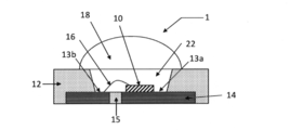
- the semiconductor light emitting device 1 of the present invention includes a reflector 12 having a concave cavity, at least one optical semiconductor element 10 provided on the bottom surface of the concave part, a pad portion 13a for mounting the optical semiconductor element, and an optical A substrate 14 having a lead portion 13b for electrical connection with a semiconductor element is provided.
- the optical semiconductor element mounted on the pad portion is electrically connected to the lead portion by a lead wire 16.
- the cavity may be a gap, but from the viewpoint of preventing electrical problems and protecting the optical semiconductor element from moisture and dust, the optical semiconductor element is sealed and emitted from the optical semiconductor element.
- a resin capable of transmitting light to the outside is filled.
- the sealing resin may contain a substance that converts the wavelength of light, such as a phosphor, if necessary.
- a lens 18 for condensing the light emitted from the optical semiconductor element may be provided on the reflector 12.
- the lens is usually made of a resin, and various structures are adopted depending on the purpose and application, and may be colored as necessary. Hereinafter, each member will be described in detail.
- the substrate 14 in the semiconductor light emitting device 1 of the present invention is a thin metal plate also called a lead frame, and the material used is mainly metal (pure metal, alloy, etc.), for example, aluminum, copper, copper-nickel. -Tin alloys, iron-nickel alloys, etc. Further, the substrate may have a light reflection layer formed so as to cover part or all of the front and back surfaces.
- the light reflection layer desirably has a high reflection function for reflecting light from the optical semiconductor element. Specifically, for electromagnetic waves having a wavelength of 380 nm to 800 nm, the reflectance at each wavelength is preferably 65% to 100%, more preferably 75% to 100%, and more preferably 80% More preferably, it is 100% or less.
- the material of the light reflecting layer include silver and silver-containing alloys.
- the silver content is preferably 60% by mass or more. When the silver content is 60% by mass or more, a sufficient reflection function can be obtained. From the same viewpoint, the silver content is preferably 70% by mass or more, and more preferably 80% by mass or more.
- the thickness of the reflective layer is preferably 1 to 20 ⁇ m. If the thickness of the reflective layer is 1 ⁇ m or more, a sufficient reflection function can be obtained, and if it is 20 ⁇ m or less, it is advantageous in terms of cost and processability is improved.
- the thickness of the substrate is not particularly limited, but is preferably in the range of 0.1 to 1.0 mm.
- the substrate is formed by etching or pressing a metal plate material, and includes a pad portion on which an optical semiconductor element such as an LED chip is mounted and a lead portion that supplies power to the optical semiconductor element.
- the pad portion and the lead portion are insulated, and the optical semiconductor element is connected to the lead portion by a lead wire through processes such as wire bonding and chip bonding.
- the reflector 12 has a function of reflecting the light from the optical semiconductor element in the direction of the light output portion (in the direction of the lens 18 in FIG. 1).
- the reflector according to the present invention is formed of a resin composition containing an inorganic substance, and the diffraction angle 2 ⁇ is 0 degree in the spectrum measured by the X-ray diffraction method using the CuK ⁇ ray (wavelength 1.5418A).
- the intensity ratio (P1) of the peak intensity P1 of the diffraction peak having the maximum intensity and the peak intensity P2 of the diffraction peak having the maximum intensity in the range of the diffraction angle 2 ⁇ of more than 24 degrees to 70 degrees in the range of 24 to 24 degrees. / P2) is 0.01 or more and 1.0 or less, and the ash content is 60% by mass or more.
- the resin composition contains a site where the molecular chains of the resin are regularly arranged (crystallized).
- crystalline resins such as polyethylene, polypropylene, polymethylpentene, polyethylene oxide, polyamide, polyacetal, polyethylene terephthalate, and polyphenylene sulfide, and cross-linked products thereof.
- resin composition containing a crystallized site By using a resin composition containing a crystallized site, a reflector excellent in fatigue resistance, chemical resistance, and mechanical properties can be obtained.
- resin composition which forms the reflector of this invention resin which has the site
- other resins including an amorphous resin may be contained as a mixture.
- Examples of the resin that is easily crystallized include hydrocarbon resins.
- One of the degrees is the diffraction peak with the maximum intensity.
- 2 ⁇ 9.3 ⁇ 1 degree, 13.4 ⁇ 1 degree, 16.7 ⁇ 1 degree, or 18.3 ⁇ 1 degree has a diffraction peak with the maximum intensity.
- a resin having the above diffraction peak that is, a hydrocarbon-based resin, improves moldability and resistance to light.
- the crystallized resin contained in the resin composition forming the reflector of the present invention is not particularly limited, but the intensity is the maximum among the diffraction peaks in the range of 2 ⁇ ranging from 0 degree to 24 degrees.
- the resin composition containing polymethylpentene is excellent in moldability, workability, and heat resistance, and has high transparency, so that even when mixed, it can suppress inhibition of optical properties such as transmittance and reflectance. Is possible.
- the polymethylpentene contained in the resin composition forming the reflector may be a homopolymer of 4-methylpentene-1 or a 4-methylpentene-1 and other ⁇ -olefins such as ethylene and propylene having 2 to 2 carbon atoms. It may be a copolymer with 20 ⁇ -olefins. Furthermore, the polymethylpentene may be a crosslinked product.
- the diffraction peak in the range of 2 ⁇ exceeding 24 degrees to 70 degrees forms the reflector of the present invention. It originates in the inorganic substance contained in the resin composition.
- the inorganic substance contained in the resin composition forming the reflector of the present invention is not particularly limited, but the diffraction having the maximum intensity among the diffraction peaks in the range of 2 ⁇ exceeding 24 degrees to 70 degrees.
- Peaks 2 ⁇ 27.4 ⁇ 1 degree, 36.1 ⁇ 1 degree, 41.2 ⁇ 1 degree, 54.3 ⁇ 1 degree, 56.6 ⁇ 1 degree, 69.0 ⁇ 1 degree, 25.3 ⁇ 1 degree, 37.9 ⁇ 1 degree, 48.1 ⁇ 1 degree, 54.0 ⁇ 1 degree, 55.1 ⁇ 1 degree, 62.7 ⁇ 1 degree, 25.3 ⁇ 1 degree, 25.7 ⁇ 1 30.8 ⁇ 1 degree, 36.3 ⁇ 1 degree, 48.0 ⁇ 1 degree, 54.2 ⁇ 1 degree, or 55.2 ⁇ 1 degree, preferably (1) It is more preferable to have any combination of (3) to (3).
- a diffraction peak of at least 2 ⁇ 27.4 ⁇ 1 degree, 36.1 ⁇ 1 degree, 41.2 ⁇ 1 degree, 54.3 ⁇ 1 degree, 56.6 ⁇ 1 degree, 69.0 ⁇ 1 degree
- at least 2 ⁇ 25.3 ⁇ 1 degree, 37.9 ⁇ 1 degree, 48.1 ⁇ 1 degree, 54.0 ⁇ 1 degree, 55.1 ⁇ 1 degree, 62.7 ⁇ 1 degree
- Combination of diffraction peaks (3)
- At least 2 ⁇ 25.3 ⁇ 1 degree, 25.7 ⁇ 1 degree, 30.8 ⁇ 1 degree, 36.3 ⁇ 1 degree, 48.0 ⁇ 1 degree, 54.2 ⁇ 1 Degree, 55.2 ⁇ 1 degree diffraction peak combination
- the peaks are attributed to the (110) plane, (101) plane, (111) plane, (211) plane, (220) plane, and (301) plane of the rutile crystal of titanium oxide, respectively.
- 2 ⁇ 25.3 ⁇ 1 degree, 37.9 ⁇ 1 degree, 48.1 ⁇ 1 degree, 54.0 ⁇ 1 degree, 55.1 ⁇ 1 degree, 62.7 ⁇ 1 degree
- 2 ⁇ 25.3 ⁇ 1 degree, 25.7 ⁇ 1 degree, 30.8 ⁇ 1 degree, 36.3 ⁇ 1 degree, 48.0 ⁇ 1 degree, and 54.2 ⁇ 1 degree in the above (3).
- 55.2 ⁇ 1 degree diffraction peaks are respectively (120) plane, (111) plane, (121) plane, (012) plane, (231) plane, (320) plane of titanium oxide brookite-type crystal, (241) plane.
- the peak intensity ratio (P1 / P2) is 0.01 or more and 1.0 or less. If the peak intensity ratio (P1 / P2) is less than 0.01, the reflector becomes brittle, and if it exceeds 1.0, sufficient dimensional stability cannot be obtained. From the above viewpoint, the peak intensity ratio (P1 / P2) is preferably in the range of 0.05 or more and 0.75 or less, and more preferably in the range of 0.1 or more and 0.5 or less.
- the average particle size of the titanium oxide contained in the resin composition forming the reflector of the present invention is 0.05 to 0.50 ⁇ m in terms of primary particle size in consideration of moldability and high reflectivity. Is more preferably 0.10 to 0.40 ⁇ m, and further preferably 0.15 to 0.30 ⁇ m.
- the average particle diameter of titanium oxide can be calculated
- the diffraction peak intensity ratio (P1 / P2) of the reflector of the present invention can be measured by an X-ray diffractometer.
- the peak intensities P1 and P2 are integrated values of the respective X-ray diffraction peaks.
- X-ray diffraction measurement conditions Radiation source: CuK ⁇ ray (wavelength: 1.5418A) Scanning axis; 2 ⁇ / ⁇ Tube voltage: 45 kV Tube current: 200 mA Slit; slitr 5.0 degrees scan speed; 5.5 degrees / minute scan step; 0.05 degrees
- the reflector of the present invention requires that the ash content is 60% by mass or more.
- the ash content is preferably 70% by mass or more, and more preferably 75% by mass or more.
- the ash content of the reflector of the present invention can be obtained by measuring only the reflector from the semiconductor light emitting device or the optical semiconductor mounting substrate as a measurement sample, and is a method defined as a general method for determining the ash content of a resin composition ( It can be measured according to JIS K 7250-1 (ISO 3451-1)) and a method based thereon or the TG-DTA method. Among these measuring methods, it is preferable to measure by JIS K 7250-1 (ISO 3451-1) and a method based thereon.
- JIS K 7250-1 (ISO 3451-1) and the method based thereon require a very large amount of sample, if a sufficient amount of sample cannot be obtained, the TG-DTA method can be used. Good.
- the measurement conditions for ash are described below.
- (2) TG-DTA method thermogravimetric / differential thermal analyzer (TG-DTA) was used to measure the mass of the sample to be measured. After heating up to 600 ° C. in minutes, the sample is incinerated by heating at 600 ° C. for 30 minutes. The mass after heating with respect to the mass before heating is expressed as a percentage, and the value is defined as ash.
- the weight ratio of all the inorganic substances including the inorganic substance in which the diffraction peak does not appear in the X-ray diffraction method in the resin composition forming the reflector can be known by measuring the ash content.
- a resin composition containing an inorganic substance a reflector having excellent reflectivity, mechanical properties, and dimensional stability can be obtained.
- those having the effect of obtaining high reflectivity include, for example, titanium oxide, zinc sulfide, zinc oxide, barium sulfide, titanium Potassium acid and the like may be mentioned, and these may be contained alone or in combination, but from the viewpoint of obtaining particularly high reflectivity, it is preferable that titanium oxide is contained, and the crystal type thereof is a rutile type. It is more preferable that
- oxides such as silica, hydroxides such as calcium hydroxide, carbonates such as calcium carbonate, sulfates such as barium sulfate, silicates such as talc, mica and wollastonite
- shapes such as a particle shape and a fiber shape, an irregular cross-sectional fiber shape, a shape with a large unevenness difference, and a thin flake shape. These may be contained alone or in combination.
- inorganic substance which can acquire the high mechanical characteristic and dimensional stability contained in the resin composition which forms the reflector of this invention is a silica particle or glass fiber. Is preferable from the viewpoint of transparency and toughness. Although these have the feature that diffraction peaks are difficult to detect in X-ray diffraction measurement, the weight of all inorganic substances including inorganic substances that can detect diffraction peaks in X-ray diffraction measurement by measuring ash content. It can be detected as a ratio.
- a dispersant may be mixed within a range that does not impair the effects of the present invention.
- the dispersant those generally used for a resin composition containing an inorganic substance can be used, and a silane coupling agent is preferred.
- the silane coupling agent has high dispersibility and compatibility of the inorganic substance with respect to the resin, and can impart high mechanical properties and dimensional stability to the reflector.
- silane coupling agent examples include disilazane such as hexamethyldisilazane; cyclic silazane; trimethylsilane, trimethylchlorosilane, dimethyldichlorosilane, methyltrichlorosilane, allyldimethylchlorosilane, trimethoxysilane, benzyldimethylchlorosilane, Methyltrimethoxysilane, methyltriethoxysilane, isobutyltrimethoxysilane, dimethyldimethoxysilane, dimethyldiethoxysilane, trimethylmethoxysilane, hydroxypropyltrimethoxysilane, phenyltrimethoxysilane, n-butyltrimethoxysilane, n-hexadecyl Trimethoxysilane, n-octadecyltrimethoxysilane, vinyltrimethoxysilane, vinyltri
- the resin composition forming the reflector of the present invention may be mixed with a crosslinking agent within a range that does not impair the effects of the present invention.
- the crosslinking agent has a saturated or unsaturated ring structure, and at least one of the atoms forming at least one ring is an allyl group, a methacryl group, an allyl group via a linking group, and a linking group.
- Those having a structure formed by bonding to any allylic substituent of the methacrylic group via The crosslinking agent having such a structure can exhibit excellent electron beam curability and can impart excellent dimensional stability to the reflector, particularly when used in combination with an electron beam curable resin.
- Examples of the saturated or unsaturated ring structure include a cyclo ring, a hetero ring, and an aromatic ring.
- the number of atoms forming the ring structure is preferably 3 to 12, more preferably 5 to 8, and still more preferably a 6-membered ring.
- Examples of the linking group include an ester bond, an ether bond, an alkylene group, and a (hetero) arylene group.
- triallyl isocyanurate methyl diallyl isocyanurate, diallyl monoglycidyl isocyanuric acid, monoallyl diglycidyl isocyanurate, trimethallyl isocyanurate, diallyl ester of orthophthalic acid, diallyl ester of isophthalic acid and the like.
- the molecular weight of the crosslinking agent is preferably 1000 or less, more preferably 500 or less, and even more preferably 300 or less, from the viewpoints of good dispersibility in the resin composition and causing an effective crosslinking reaction. .
- the number of ring structures is preferably 1 to 3, more preferably 1 or 2, and further preferably 1.
- the content of the crosslinking agent is preferably 0.5 to 40 parts by mass with respect to 100 parts by mass of the resin. With this content, good curability can be imparted without bleeding out. From the above viewpoint, the content of the crosslinking agent is more preferably 1 to 30 parts by mass, and particularly preferably 5 to 20 parts by mass.
- the resin composition forming the reflector of the present invention may contain various additives as long as the effects of the present invention are not impaired.
- the resin composition forming the reflector of the present invention can be prepared by mixing a resin, an inorganic substance, a crosslinking agent added as necessary, and other additives in a predetermined ratio.
- a known means such as a two-roll or three-roll, a homogenizer, a planetary mixer, a stirrer such as a twin-screw kneading extruder, a melt kneader such as a polylab system or a lab plast mill, etc. is applied.
- a known means such as a two-roll or three-roll, a homogenizer, a planetary mixer, a stirrer such as a twin-screw kneading extruder, a melt kneader such as a polylab system or a lab plast mill, etc. is applied.
- a stirrer such as a twin-screw kneading extruder, a melt kneader such as
- the shape of the reflector 12 conforms to the shape of the end portion (joint portion) of the lens 18 and is usually a cylindrical shape such as a square shape, a circular shape, or an oval shape, or an annular shape.
- the reflector 12 is a cylindrical body (annular body), and all the end faces of the reflector 12 are in contact with and fixed to the surface of the substrate 14.
- the reflector 12 has a shape having a recessed cavity, and the inner surface of the reflector 12 may be widened upward in a tapered shape in order to increase the directivity of light from the optical semiconductor element 10.
- the reflector 12 can also function as a lens holder when the end portion on the lens 18 side is processed into a shape corresponding to the shape of the lens 18.
- the cylinder temperature is preferably 200 to 400 ° C., more preferably 220 to 320 ° C. from the viewpoint of moldability.
- the mold temperature is preferably 10 to 170 ° C, more preferably 20 to 150 ° C.
- the reflector according to the present invention may be subjected to ionizing radiation irradiation treatment before or after the molding step, and among them, electron beam irradiation treatment is preferable. By performing the electron beam irradiation treatment, the mechanical properties and dimensional stability of the reflector can be improved.
- the cavity of the reflector according to the present invention is preferably sealed with a resin (sealing resin) capable of sealing the optical semiconductor element and transmitting light emitted from the optical semiconductor element to the outside.
- a resin sealing resin
- the lead wire is disconnected from the connection portion with the optical semiconductor element and / or the connection portion with the electrode due to the force applied by direct contact with the lead wire and the vibration or impact applied indirectly. It is possible to prevent electrical problems caused by cutting, cutting, or short-circuiting.
- the optical semiconductor element can be protected from moisture, dust, etc., and the reliability can be maintained for a long time.
- sealing resin is not specifically limited, Silicone resin, epoxy silicone resin, epoxy resin, acrylic resin, polyimide resin, polycarbonate resin, etc. are mentioned. Of these, silicone resins are preferred from the viewpoints of heat resistance, weather resistance, low shrinkage, and discoloration resistance. Furthermore, the sealing resin may contain a substance that converts the wavelength of light, such as a phosphor, as necessary.
- An optical semiconductor device emits radiated light (generally UV or blue light in a white light LED), for example, an active layer made of AlGaAs, AlGaInP, GaP or GaN sandwiched between n-type and p-type cladding layers
- a semiconductor chip (light emitter) having a double heterostructure, for example, has a hexahedral shape with a side length of about 0.5 mm. And in the case of the form of wire bonding mounting, it is connected to the lead part via the lead wire.
- the substrate for mounting an optical semiconductor according to the present invention is suitably used for the semiconductor light emitting device, and includes a substrate 14 and a reflector 12 having a concave cavity.
- the reflector is formed of a resin composition containing an inorganic substance, and in the spectrum measured by the X-ray diffraction method using the CuK ⁇ ray (wavelength 1.5418A), the reflector has a diffraction angle 2 ⁇ .
- the intensity ratio between the peak intensity P1 of the diffraction peak having the maximum intensity in the range of 0 to 24 degrees and the peak intensity P2 of the diffraction peak having the maximum intensity in the range of the diffraction angle 2 ⁇ of more than 24 degrees to 70 degrees. (P1 / P2) is 0.01 or more and 1.0 or less, and the ash content of the reflector is 60% by mass or more.
- a resin composition for forming a reflector on a substrate (metal frame or lead frame) 14 is molded by transfer molding, compression molding, injection molding or the like using a mold having a cavity space of a predetermined shape, A molded body having a plurality of shaped reflectors is obtained. Since a plurality of reflectors can be produced simultaneously, it is efficient and injection molding is a preferred method. The molded body thus obtained may undergo a curing process such as electron beam irradiation as necessary.
- a substrate on which a reflector is placed is an optical semiconductor mounting substrate (FIG. 2A).
- a separately prepared optical semiconductor element 10 such as an LED chip is disposed on the optical semiconductor mounting substrate (FIG. 2B).
- an adhesive or a bonding member may be used to fix the optical semiconductor element 10.
- a lead wire 16 is provided to electrically connect the optical semiconductor element and the lead portion (electrode). In that case, in order to improve the connection of the lead wire, it is preferable to heat at 100 to 250 ° C. for 5 to 20 minutes.
- FIG. 2D a sealing resin is filled in the cavity of the reflector and cured to produce the sealing portion 22.
- the semiconductor light emitting device shown in FIG. 1 is obtained by dividing into pieces by a method such as dicing at the substantially center (dotted line portion) of the reflector.
- the lens 18 can be disposed on the sealing portion 22 as necessary.
- the sealing resin may be cured after the lens 18 is placed in a state where the sealing resin is uncured.
- FIG. 2F shows the semiconductor light emitting device connected to the wiring board 24 and mounted.
- a method for mounting the semiconductor light emitting device on the wiring board is not particularly limited, but it is preferable to use a melted solder.
- solder is provided on a wiring board, a package is placed on the solder, and then heated to 220 to 270 ° C., which is a general solder melting temperature, in a reflow furnace to melt the solder. And mounting the semiconductor light emitting device on the wiring substrate (solder reflow method).
- solder reflow method A well-known thing can be used for the solder used by the method using said solder.
- Production Example 2 In Production Example 1, a resin composition 2 was obtained in the same manner as in Production Example 1 except that the content of TiO 2 was changed to 350 parts by mass and the blending amount of the dispersant was 5 parts by mass. As in Production Example 1, the formulation is shown in Table 1.
- Production Example 3 In Production Example 1, Production Example 1 except that the content of TiO 2 was changed to 200 parts by mass, the amount of dispersant was 5 parts by mass, and the amount of TAIC was 12 parts by mass. Similarly, a resin composition 3 was obtained. As in Production Example 1, the formulation is shown in Table 1.
- Production Example 4 In Production Example 3, the blending amount of IRGANOX1010 (BASF Japan Co., Ltd.), which is an antioxidant, was 1 part by mass, and 0.5 part by mass of IRGAFOS168 (BASF Japan Co., Ltd.) was blended. A resin composition 4 was obtained in the same manner as in Production Example 3 except that 1 part by mass of KBM-303 (manufactured by Shin-Etsu Silicone Co., Ltd.) was added as a dispersant. As in Production Example 1, the formulation is shown in Table 1.
- Production Example 5 In Production Example 1, a resin composition 5 was obtained in the same manner as in Production Example 1 except that the amount of TAIC was 18 parts by mass. As in Production Example 1, the formulation is shown in Table 1.
- Production Example 6 In Production Example 5, instead of PF70E-001 as a glass fiber, SS05DE-413SP (manufactured by Nitto Boseki Co., Ltd., average fiber length 100 ⁇ m, average fiber diameter 6 ⁇ m) was used except that 120 parts by mass was blended. Thus, a resin composition 6 was obtained. As in Production Example 1, the formulation is shown in Table 1.
- Production Example 7 In Production Example 6, the same procedure as in Production Example 6 was used except that polymethylpentene TPX MX002 (manufactured by Mitsui Chemicals, Inc., weight average molecular weight 500,000 to 700,000) was used as the resin instead of polymethylpentene TPX RT18. Thus, a resin composition 7 was obtained. As in Production Example 1, the formulation is shown in Table 1.
- Production Example 8 In Production Example 5, the same procedure as in Production Example 5 was used except that polymethylpentene TPX DX820 (manufactured by Mitsui Chemicals, Inc., weight average molecular weight 150,000 to 350,000) was used instead of polymethylpentene TPX RT18 as the resin. Thus, a resin composition 8 was obtained. As in Production Example 1, the formulation is shown in Table 1.
- Production Example 9 In Production Example 5, the same procedure as in Production Example 5 was used except that polymethylpentene TPX DX231 (Mitsui Chemicals, Inc., weight average molecular weight 200,000 to 400,000) was used instead of polymethylpentene TPX RT18 as the resin. Thus, a resin composition 9 was obtained.
- the formulation is shown in Table 2.
- Production Example 10 In Production Example 5, a resin composition 10 was obtained in the same manner as in Production Example 5 except that polyethylene hyzex 1300J (manufactured by Prime Polymer Co., Ltd.) was used instead of polymethylpentene TPX RT18 as the resin. The formulation is shown in Table 2 in the same manner as in Production Example 9.
- Production Example 11 In Production Example 5, a resin composition 11 was obtained in the same manner as in Production Example 5 except that polypropylene prime polypro J137G (manufactured by Prime Polymer Co., Ltd.) was used instead of polymethylpentene TPX RT18 as the resin. As in Production Example 9, the formulation is shown in Table 2.
- Comparative production example 1 In Production Example 4, Comparative Resin Composition 1 was obtained in the same manner as Production Example 4 except that no glass fiber was added. As in Production Example 9, the formulation is shown in Table 2.
- Comparative production example 2 In Production Example 4, the comparative resin composition 2 was prepared in the same manner as in Production Example 4 except that the blending amount of TiO 2 was 100 parts by mass, the TAIC content was 4 parts by mass, and no glass fiber was blended. Obtained. As in Production Example 9, the formulation is shown in Table 2.
- Comparative production example 3 In Production Example 4, the compounding amount of TiO 2 was 45 parts by mass, the TAIC content was 4 parts by mass, and the glass fiber was CSG3PA-820 (manufactured by Nitto Boseki Co., Ltd., average fiber length 3 mm, modified) Comparative resin composition 3 was obtained in the same manner as in Production Example 4 except that 60 parts by mass of ratio 4) was blended. As in Production Example 9, the formulation is shown in Table 2.
- Comparative production example 4 In Production Example 1, a comparative resin composition 4 was obtained in the same manner as in Production Example 1 except that TiO 2 was not blended and the TAIC content was 6 parts by mass. As in Production Example 9, the formulation is shown in Table 2.
- Each of the resin compositions 1 to 11 prepared in Production Examples 1 to 11 is made of copper, which is silver-plated as a light reflecting layer by an injection molding machine TR55EH (manufactured by Sodick Co., Ltd., screw diameter ⁇ 22 mm).
- TR55EH injection molding machine
- a molded body having a plurality of reflectors having outer dimensions: 30 mm ⁇ 30 mm and thickness: 0.35 mm was obtained.
- the injection molding conditions were appropriately set between a cylinder temperature of 220 to 320 ° C. and a mold temperature of 20 to 150 ° C. according to the resin composition.
- Each molded body was irradiated with an electron beam at an acceleration voltage of 800 kV and an absorbed dose of 400 kGy to obtain a substrate for mounting an optical semiconductor.
- Separately prepared LED elements (light emission color: blue) were arranged on the pad portions of the respective optical semiconductor mounting substrates produced as described above, and fixed with an adhesive. The LED element and the lead part were connected with the lead wire and then diced into individual pieces to obtain a semiconductor light emitting device.
- Comparative Examples 1 to 4 Using the comparative resin compositions 1 to 4 prepared in Comparative Production Examples 1 to 4, an optical semiconductor mounting substrate and a semiconductor light emitting device were obtained in the same manner as in the Examples.
- Ash content The measurement sample was obtained by cutting out only the reflector from the substrate for mounting an optical semiconductor produced in each example and comparative example, and the method A (direct ashing method) of JIS K 7250-1 (ISO 3451-1) ), The ash content was measured as follows. First, the crucible was heated to a constant weight in a muffle furnace heated to 800 ° C. (FO310 manufactured by Yamato Scientific Co., Ltd.), and then cooled to room temperature in a desiccator. Subsequently, the mass of the crucible was measured to an order of 0.1 mg with an electronic small balance (AG104 manufactured by METTLER TOLEDO).
- the sample was pre-dried at 60 ° C for 2 to 5 hours with a ventilation constant temperature thermostat (DKM400 manufactured by Yamato Kagaku Co., Ltd.), then transferred to a crucible, and the mass was measured to an order of 0.1 mg with a small electronic balance.
- the mass of the sample before ashing was obtained by subtracting the mass of the crucible from the value.
- the mass of the sample after ashing with respect to the mass of the sample before ashing was expressed as a percentage, and the value was defined as ash.
- the measurement results are shown in Tables 3 and 4.
- the reflectance of the reflector at a wavelength of 230 to 780 nm is measured using a reflectance measuring device MCPD-9800 (manufactured by Otsuka Electronics Co., Ltd.). Measured. Tables 3 and 4 show the results of reflectance at a wavelength of 450 nm.
- the same semiconductor light emitting device was allowed to emit light continuously at a constant current of 200 mA in an environment of a temperature of 85 ° C. and a humidity of 85% RH.
- the luminous flux emitted at a constant current of 200 mA after a cumulative time of 500 hours is measured with an instantaneous multi-photometry system (wide dynamic range type) MCPD-9800 (manufactured by Otsuka Electronics Co., Ltd.), and the luminous flux after 500 hours ( ⁇ 500 ) It was. From the measured initial luminous flux ( ⁇ 0 ) and the luminous flux after 500 hours ( ⁇ 500 ), the luminous flux deterioration rate was calculated according to the following formula A.
- Luminous flux degradation rate (%)
- Tables 3 and 4 show the luminous flux deterioration rates calculated from the initial luminous flux ( ⁇ 0 ) and the luminous flux after 500 hours ( ⁇ 500 ).
- Comparative Examples 1 to 11 since the dimensional stability was 1% or less, the reflectance was 90% or more, and the luminous flux deterioration rate after a high-temperature and high-humidity operation test was 3% or less, good performance as a semiconductor light emitting device was obtained. It was. On the other hand, Comparative Examples 1 to 3 had a dimensional stability of 10% or more and a luminous flux deterioration rate of 10% or more after the high-temperature and high-humidity operation test, so that sufficient performance as a semiconductor light emitting device could not be satisfied. Furthermore, since Comparative Example 4 had a dimensional stability of 10% or more and a reflectance of 46%, the performance sufficient as a semiconductor light emitting device could not be satisfied.
- a semiconductor light emitting device including at least a substrate, a reflector having a concave cavity, and an optical semiconductor element, the reflector is formed of a resin composition containing an inorganic substance, and the reflector is formed of CuK ⁇
- the peak intensity P1 and diffraction angle 2 ⁇ of the diffraction peak having the maximum intensity in the range where the diffraction angle 2 ⁇ is 0 degree to 24 degrees are
- the intensity ratio (P1 / P2) of the peak intensity P2 of the diffraction peak having the maximum intensity in the range of more than 24 degrees to 70 degrees is 0.01 or more and 1.0 or less, and the ash content is 60 mass% or more.
- the present invention it is possible to provide a semiconductor light emitting device and an optical semiconductor mounting substrate in which the reflector has extremely high reflectivity and is excellent in dimensional stability.
- SYMBOLS 1 Semiconductor light-emitting device 10; Semiconductor element 12; Reflector 13a; Pad part 13b; Lead part 14; Substrate (metal frame, lead frame) 15; Insulating part 16; Lead wire 18; Lens 22; Sealing part 24;
Landscapes
- Engineering & Computer Science (AREA)
- Computer Hardware Design (AREA)
- Microelectronics & Electronic Packaging (AREA)
- Power Engineering (AREA)
- Led Device Packages (AREA)
Priority Applications (3)
| Application Number | Priority Date | Filing Date | Title |
|---|---|---|---|
| US15/129,848 US10411174B2 (en) | 2014-03-31 | 2015-03-27 | Semiconductor light-emitting device and optical-semiconductor-mounting substrate |
| CN201580017903.3A CN106133929B (zh) | 2014-03-31 | 2015-03-27 | 半导体发光装置及光半导体安装用基板 |
| KR1020167026854A KR20160140660A (ko) | 2014-03-31 | 2015-03-27 | 반도체 발광 장치 및 광 반도체 실장용 기판 |
Applications Claiming Priority (4)
| Application Number | Priority Date | Filing Date | Title |
|---|---|---|---|
| JP2014074828 | 2014-03-31 | ||
| JP2014-074828 | 2014-03-31 | ||
| JP2015-017933 | 2015-01-30 | ||
| JP2015017933A JP5920497B2 (ja) | 2014-03-31 | 2015-01-30 | 半導体発光装置及び光半導体実装用基板 |
Publications (1)
| Publication Number | Publication Date |
|---|---|
| WO2015152097A1 true WO2015152097A1 (ja) | 2015-10-08 |
Family
ID=54240420
Family Applications (1)
| Application Number | Title | Priority Date | Filing Date |
|---|---|---|---|
| PCT/JP2015/059784 Ceased WO2015152097A1 (ja) | 2014-03-31 | 2015-03-27 | 半導体発光装置及び光半導体実装用基板 |
Country Status (6)
| Country | Link |
|---|---|
| US (1) | US10411174B2 (enExample) |
| JP (1) | JP5920497B2 (enExample) |
| KR (1) | KR20160140660A (enExample) |
| CN (1) | CN106133929B (enExample) |
| TW (1) | TW201601353A (enExample) |
| WO (1) | WO2015152097A1 (enExample) |
Families Citing this family (5)
| Publication number | Priority date | Publication date | Assignee | Title |
|---|---|---|---|---|
| KR102221601B1 (ko) * | 2014-10-17 | 2021-03-02 | 엘지이노텍 주식회사 | 발광 소자 패키지 및 이를 포함하는 발광 모듈 |
| US10164159B2 (en) * | 2016-12-20 | 2018-12-25 | Samsung Electronics Co., Ltd. | Light-emitting diode package and method of manufacturing the same |
| JP2020055910A (ja) * | 2018-09-28 | 2020-04-09 | 日亜化学工業株式会社 | 樹脂組成物、及び発光装置 |
| WO2020232668A1 (en) * | 2019-05-22 | 2020-11-26 | Cree Huizhou Solid State Lighting Company Limited | Arrangements for light emitting diode packages |
| TWI692816B (zh) * | 2019-05-22 | 2020-05-01 | 友達光電股份有限公司 | 顯示裝置及其製作方法 |
Citations (4)
| Publication number | Priority date | Publication date | Assignee | Title |
|---|---|---|---|---|
| JP2013077794A (ja) * | 2011-09-16 | 2013-04-25 | Sekisui Chem Co Ltd | 光半導体装置 |
| JP2013232532A (ja) * | 2012-04-27 | 2013-11-14 | Dainippon Printing Co Ltd | 光反射積層体及び半導体発光装置 |
| JP2013243294A (ja) * | 2012-05-22 | 2013-12-05 | Kaneka Corp | 半導体パッケージの製造方法 |
| JP2013249239A (ja) * | 2012-06-01 | 2013-12-12 | Nichia Corp | 発光素子載置用基板及び発光装置 |
Family Cites Families (11)
| Publication number | Priority date | Publication date | Assignee | Title |
|---|---|---|---|---|
| JPH0560707A (ja) | 1991-09-02 | 1993-03-12 | Nippon Steel Corp | 石炭の膨張性試験方法 |
| JP2006070252A (ja) * | 2004-08-03 | 2006-03-16 | Mitsui Chemicals Inc | ポリ4−メチル−1−ペンテン樹脂組成物、フィルムおよび電子部品封止体製造用型枠 |
| JP5060707B2 (ja) | 2004-11-10 | 2012-10-31 | 日立化成工業株式会社 | 光反射用熱硬化性樹脂組成物 |
| CN101400492B (zh) * | 2006-03-20 | 2012-07-25 | 三井化学株式会社 | 光学膜及其制造方法 |
| JP2008144155A (ja) * | 2006-11-14 | 2008-06-26 | Mitsui Chemicals Inc | 4−メチル−1−ペンテン系ランダム共重合体およびその製造方法ならびに該共重合体を含む組成物 |
| EP2476731B1 (en) | 2009-09-07 | 2016-07-20 | Kuraray Co., Ltd. | Reflector for led and light-emitting device equipped with same |
| JP5416629B2 (ja) | 2010-03-19 | 2014-02-12 | 住友電気工業株式会社 | 白色樹脂成形体及びled用リフレクタ |
| JP5545246B2 (ja) * | 2010-03-30 | 2014-07-09 | 信越化学工業株式会社 | 樹脂組成物及び発光半導体素子用リフレクター、及び発光半導体装置 |
| US8704439B2 (en) * | 2010-09-07 | 2014-04-22 | Ube Material Industries, Ltd. | Blue-light-emitting phosphor and light-emitting device equipped with the blue-light-emitting phosphor |
| US9975284B2 (en) * | 2012-01-17 | 2018-05-22 | Dai Nipon Printing Co., Ltd. | Electron beam curable resin composition, resin frame for reflectors, reflector, semiconductor light emitting device, and method for producing molded body |
| JP2014199285A (ja) * | 2013-03-29 | 2014-10-23 | 積水化成品工業株式会社 | 光反射板 |
-
2015
- 2015-01-30 JP JP2015017933A patent/JP5920497B2/ja not_active Expired - Fee Related
- 2015-03-27 CN CN201580017903.3A patent/CN106133929B/zh not_active Expired - Fee Related
- 2015-03-27 KR KR1020167026854A patent/KR20160140660A/ko not_active Withdrawn
- 2015-03-27 US US15/129,848 patent/US10411174B2/en not_active Expired - Fee Related
- 2015-03-27 WO PCT/JP2015/059784 patent/WO2015152097A1/ja not_active Ceased
- 2015-03-30 TW TW104110278A patent/TW201601353A/zh unknown
Patent Citations (4)
| Publication number | Priority date | Publication date | Assignee | Title |
|---|---|---|---|---|
| JP2013077794A (ja) * | 2011-09-16 | 2013-04-25 | Sekisui Chem Co Ltd | 光半導体装置 |
| JP2013232532A (ja) * | 2012-04-27 | 2013-11-14 | Dainippon Printing Co Ltd | 光反射積層体及び半導体発光装置 |
| JP2013243294A (ja) * | 2012-05-22 | 2013-12-05 | Kaneka Corp | 半導体パッケージの製造方法 |
| JP2013249239A (ja) * | 2012-06-01 | 2013-12-12 | Nichia Corp | 発光素子載置用基板及び発光装置 |
Also Published As
| Publication number | Publication date |
|---|---|
| JP2015201623A (ja) | 2015-11-12 |
| KR20160140660A (ko) | 2016-12-07 |
| CN106133929A (zh) | 2016-11-16 |
| US10411174B2 (en) | 2019-09-10 |
| CN106133929B (zh) | 2018-10-26 |
| TW201601353A (zh) | 2016-01-01 |
| US20170207376A1 (en) | 2017-07-20 |
| JP5920497B2 (ja) | 2016-05-18 |
Similar Documents
| Publication | Publication Date | Title |
|---|---|---|
| JP6277963B2 (ja) | 電子線硬化性樹脂組成物、リフレクター用樹脂フレーム、リフレクター、半導体発光装置、及び成形体の製造方法 | |
| US9975284B2 (en) | Electron beam curable resin composition, resin frame for reflectors, reflector, semiconductor light emitting device, and method for producing molded body | |
| JP5920497B2 (ja) | 半導体発光装置及び光半導体実装用基板 | |
| TWI644957B (zh) | Resin composition, reflector, lead frame with reflector, and semiconductor light emitting device | |
| WO2012039434A1 (ja) | 反射材組成物、反射体及び半導体発光装置 | |
| JP6102413B2 (ja) | 電子線硬化性樹脂組成物、リフレクター用樹脂フレーム、リフレクター、半導体発光装置、及び成形体の製造方法 | |
| JP6277592B2 (ja) | リフレクター用電子線硬化性樹脂組成物、リフレクター用樹脂フレーム、リフレクター、半導体発光装置、成形体の製造方法、及び半導体発光装置の製造方法 | |
| JP5168337B2 (ja) | 反射材組成物、反射体及び半導体発光装置 | |
| JP2017069348A (ja) | 半導体発光装置、光半導体実装用基板及びリフレクター | |
| JP6167603B2 (ja) | 電子線硬化性樹脂組成物、リフレクター用樹脂フレーム、リフレクター、半導体発光装置、成形体の製造方法、及び半導体発光装置の製造方法 | |
| JP6292130B2 (ja) | 電子線硬化性樹脂組成物、リフレクター用樹脂フレーム、リフレクター、半導体発光装置、及び成形体の製造方法 | |
| JP6149457B2 (ja) | 光半導体実装用基板、半導体発光装置、及び光半導体実装用基板の製造方法 | |
| JP6155929B2 (ja) | 半導体発光装置、半導体発光装置用部品及びそれらの製造方法、並びに反射体及びその製造方法 | |
| WO2016017818A1 (ja) | リフレクター及び樹脂組成物 | |
| JP6094412B2 (ja) | 半導体発光装置の製造方法、成形体の製造方法、電子線硬化性樹脂組成物、リフレクター用樹脂フレーム、およびリフレクター | |
| JP2015023099A (ja) | 半導体発光装置の製造方法、成形体の製造方法、電子線硬化性樹脂組成物、リフレクター用樹脂フレーム、およびリフレクター | |
| WO2015152098A1 (ja) | 半導体発光装置及び光半導体実装用基板 | |
| JP2016035010A (ja) | 樹脂組成物、リフレクター、リフレクター付きリードフレーム及び半導体発光装置 | |
| JP2016036028A (ja) | リフレクター、リフレクター付きリードフレーム、半導体発光装置、及び樹脂組成物 |
Legal Events
| Date | Code | Title | Description |
|---|---|---|---|
| 121 | Ep: the epo has been informed by wipo that ep was designated in this application |
Ref document number: 15772602 Country of ref document: EP Kind code of ref document: A1 |
|
| ENP | Entry into the national phase |
Ref document number: 20167026854 Country of ref document: KR Kind code of ref document: A |
|
| WWE | Wipo information: entry into national phase |
Ref document number: 15129848 Country of ref document: US |
|
| NENP | Non-entry into the national phase |
Ref country code: DE |
|
| 122 | Ep: pct application non-entry in european phase |
Ref document number: 15772602 Country of ref document: EP Kind code of ref document: A1 |