WO2015152097A1 - 半導体発光装置及び光半導体実装用基板 - Google Patents
半導体発光装置及び光半導体実装用基板 Download PDFInfo
- Publication number
- WO2015152097A1 WO2015152097A1 PCT/JP2015/059784 JP2015059784W WO2015152097A1 WO 2015152097 A1 WO2015152097 A1 WO 2015152097A1 JP 2015059784 W JP2015059784 W JP 2015059784W WO 2015152097 A1 WO2015152097 A1 WO 2015152097A1
- Authority
- WO
- WIPO (PCT)
- Prior art keywords
- degree
- degrees
- diffraction
- reflector
- emitting device
- Prior art date
Links
- 239000004065 semiconductor Substances 0.000 title claims abstract description 131
- 239000000758 substrate Substances 0.000 title claims abstract description 58
- 230000003287 optical effect Effects 0.000 claims abstract description 64
- 239000011342 resin composition Substances 0.000 claims abstract description 61
- 239000000126 substance Substances 0.000 claims abstract description 31
- 238000002441 X-ray diffraction Methods 0.000 claims abstract description 19
- 238000001228 spectrum Methods 0.000 claims abstract description 12
- 238000000034 method Methods 0.000 claims description 44
- 229920005989 resin Polymers 0.000 claims description 36
- 239000011347 resin Substances 0.000 claims description 36
- 238000007789 sealing Methods 0.000 claims description 15
- 239000003431 cross linking reagent Substances 0.000 claims description 12
- 238000002310 reflectometry Methods 0.000 abstract description 9
- 230000005855 radiation Effects 0.000 abstract description 3
- 238000004519 manufacturing process Methods 0.000 description 67
- GWEVSGVZZGPLCZ-UHFFFAOYSA-N Titan oxide Chemical compound O=[Ti]=O GWEVSGVZZGPLCZ-UHFFFAOYSA-N 0.000 description 24
- 239000000203 mixture Substances 0.000 description 19
- 230000000052 comparative effect Effects 0.000 description 18
- 229920000306 polymethylpentene Polymers 0.000 description 18
- 239000011116 polymethylpentene Substances 0.000 description 18
- 238000009472 formulation Methods 0.000 description 16
- -1 polyethylene Polymers 0.000 description 16
- 229910000679 solder Inorganic materials 0.000 description 15
- OGIDPMRJRNCKJF-UHFFFAOYSA-N titanium oxide Inorganic materials [Ti]=O OGIDPMRJRNCKJF-UHFFFAOYSA-N 0.000 description 15
- 238000010438 heat treatment Methods 0.000 description 14
- 230000004907 flux Effects 0.000 description 13
- 238000005259 measurement Methods 0.000 description 10
- WABPQHHGFIMREM-UHFFFAOYSA-N lead(0) Chemical compound [Pb] WABPQHHGFIMREM-UHFFFAOYSA-N 0.000 description 9
- 238000004380 ashing Methods 0.000 description 8
- KOMNUTZXSVSERR-UHFFFAOYSA-N 1,3,5-tris(prop-2-enyl)-1,3,5-triazinane-2,4,6-trione Chemical compound C=CCN1C(=O)N(CC=C)C(=O)N(CC=C)C1=O KOMNUTZXSVSERR-UHFFFAOYSA-N 0.000 description 7
- 239000013078 crystal Substances 0.000 description 7
- 239000002270 dispersing agent Substances 0.000 description 7
- 238000010894 electron beam technology Methods 0.000 description 7
- 239000000835 fiber Substances 0.000 description 7
- BQCADISMDOOEFD-UHFFFAOYSA-N Silver Chemical compound [Ag] BQCADISMDOOEFD-UHFFFAOYSA-N 0.000 description 6
- 229920005533 TPX™ RT18 Polymers 0.000 description 6
- 229910010413 TiO 2 Inorganic materials 0.000 description 6
- 230000000694 effects Effects 0.000 description 6
- 239000003365 glass fiber Substances 0.000 description 6
- 239000000463 material Substances 0.000 description 6
- 229910052751 metal Inorganic materials 0.000 description 6
- 239000002184 metal Substances 0.000 description 6
- 239000002245 particle Substances 0.000 description 6
- 229910052709 silver Inorganic materials 0.000 description 6
- 239000004332 silver Substances 0.000 description 6
- 230000006866 deterioration Effects 0.000 description 5
- 238000001746 injection moulding Methods 0.000 description 5
- 238000002156 mixing Methods 0.000 description 5
- VYPSYNLAJGMNEJ-UHFFFAOYSA-N Silicium dioxide Chemical compound O=[Si]=O VYPSYNLAJGMNEJ-UHFFFAOYSA-N 0.000 description 4
- 239000000654 additive Substances 0.000 description 4
- 229920001155 polypropylene Polymers 0.000 description 4
- 239000004952 Polyamide Substances 0.000 description 3
- 239000004698 Polyethylene Substances 0.000 description 3
- 239000004743 Polypropylene Substances 0.000 description 3
- 239000006087 Silane Coupling Agent Substances 0.000 description 3
- 239000003963 antioxidant agent Substances 0.000 description 3
- 238000005520 cutting process Methods 0.000 description 3
- 125000005647 linker group Chemical group 0.000 description 3
- 230000007774 longterm Effects 0.000 description 3
- 238000002844 melting Methods 0.000 description 3
- 230000008018 melting Effects 0.000 description 3
- 229920002647 polyamide Polymers 0.000 description 3
- 229920000573 polyethylene Polymers 0.000 description 3
- 229920001296 polysiloxane Polymers 0.000 description 3
- 229920002050 silicone resin Polymers 0.000 description 3
- 238000012360 testing method Methods 0.000 description 3
- 125000003903 2-propenyl group Chemical group [H]C([*])([H])C([H])=C([H])[H] 0.000 description 2
- WSSSPWUEQFSQQG-UHFFFAOYSA-N 4-methyl-1-pentene Chemical compound CC(C)CC=C WSSSPWUEQFSQQG-UHFFFAOYSA-N 0.000 description 2
- VTYYLEPIZMXCLO-UHFFFAOYSA-L Calcium carbonate Chemical compound [Ca+2].[O-]C([O-])=O VTYYLEPIZMXCLO-UHFFFAOYSA-L 0.000 description 2
- RYGMFSIKBFXOCR-UHFFFAOYSA-N Copper Chemical compound [Cu] RYGMFSIKBFXOCR-UHFFFAOYSA-N 0.000 description 2
- 239000013032 Hydrocarbon resin Substances 0.000 description 2
- OAICVXFJPJFONN-UHFFFAOYSA-N Phosphorus Chemical compound [P] OAICVXFJPJFONN-UHFFFAOYSA-N 0.000 description 2
- XLOMVQKBTHCTTD-UHFFFAOYSA-N Zinc monoxide Chemical compound [Zn]=O XLOMVQKBTHCTTD-UHFFFAOYSA-N 0.000 description 2
- BGYHLZZASRKEJE-UHFFFAOYSA-N [3-[3-(3,5-ditert-butyl-4-hydroxyphenyl)propanoyloxy]-2,2-bis[3-(3,5-ditert-butyl-4-hydroxyphenyl)propanoyloxymethyl]propyl] 3-(3,5-ditert-butyl-4-hydroxyphenyl)propanoate Chemical compound CC(C)(C)C1=C(O)C(C(C)(C)C)=CC(CCC(=O)OCC(COC(=O)CCC=2C=C(C(O)=C(C=2)C(C)(C)C)C(C)(C)C)(COC(=O)CCC=2C=C(C(O)=C(C=2)C(C)(C)C)C(C)(C)C)COC(=O)CCC=2C=C(C(O)=C(C=2)C(C)(C)C)C(C)(C)C)=C1 BGYHLZZASRKEJE-UHFFFAOYSA-N 0.000 description 2
- 239000000853 adhesive Substances 0.000 description 2
- 230000001070 adhesive effect Effects 0.000 description 2
- 229910045601 alloy Inorganic materials 0.000 description 2
- 239000000956 alloy Substances 0.000 description 2
- 150000001412 amines Chemical class 0.000 description 2
- 230000003078 antioxidant effect Effects 0.000 description 2
- 125000004429 atom Chemical group 0.000 description 2
- TZCXTZWJZNENPQ-UHFFFAOYSA-L barium sulfate Chemical compound [Ba+2].[O-]S([O-])(=O)=O TZCXTZWJZNENPQ-UHFFFAOYSA-L 0.000 description 2
- WPYMKLBDIGXBTP-UHFFFAOYSA-N benzoic acid Chemical compound OC(=O)C1=CC=CC=C1 WPYMKLBDIGXBTP-UHFFFAOYSA-N 0.000 description 2
- 125000004432 carbon atom Chemical group C* 0.000 description 2
- 239000003795 chemical substances by application Substances 0.000 description 2
- IJOOHPMOJXWVHK-UHFFFAOYSA-N chlorotrimethylsilane Chemical compound C[Si](C)(C)Cl IJOOHPMOJXWVHK-UHFFFAOYSA-N 0.000 description 2
- 229910052802 copper Inorganic materials 0.000 description 2
- 239000010949 copper Substances 0.000 description 2
- 238000010586 diagram Methods 0.000 description 2
- 239000000428 dust Substances 0.000 description 2
- 239000003822 epoxy resin Substances 0.000 description 2
- 125000005842 heteroatom Chemical group 0.000 description 2
- FFUAGWLWBBFQJT-UHFFFAOYSA-N hexamethyldisilazane Chemical compound C[Si](C)(C)N[Si](C)(C)C FFUAGWLWBBFQJT-UHFFFAOYSA-N 0.000 description 2
- 229920006270 hydrocarbon resin Polymers 0.000 description 2
- ZFSLODLOARCGLH-UHFFFAOYSA-N isocyanuric acid Chemical compound OC1=NC(O)=NC(O)=N1 ZFSLODLOARCGLH-UHFFFAOYSA-N 0.000 description 2
- QQVIHTHCMHWDBS-UHFFFAOYSA-N isophthalic acid Chemical compound OC(=O)C1=CC=CC(C(O)=O)=C1 QQVIHTHCMHWDBS-UHFFFAOYSA-N 0.000 description 2
- 238000004898 kneading Methods 0.000 description 2
- 238000001579 optical reflectometry Methods 0.000 description 2
- 238000005375 photometry Methods 0.000 description 2
- 229920000647 polyepoxide Polymers 0.000 description 2
- 229920000642 polymer Polymers 0.000 description 2
- 238000002360 preparation method Methods 0.000 description 2
- YGSDEFSMJLZEOE-UHFFFAOYSA-N salicylic acid Chemical compound OC(=O)C1=CC=CC=C1O YGSDEFSMJLZEOE-UHFFFAOYSA-N 0.000 description 2
- 229920006395 saturated elastomer Polymers 0.000 description 2
- 239000000377 silicon dioxide Substances 0.000 description 2
- YUYCVXFAYWRXLS-UHFFFAOYSA-N trimethoxysilane Chemical compound CO[SiH](OC)OC YUYCVXFAYWRXLS-UHFFFAOYSA-N 0.000 description 2
- 239000004711 α-olefin Substances 0.000 description 2
- WYTZZXDRDKSJID-UHFFFAOYSA-N (3-aminopropyl)triethoxysilane Chemical compound CCO[Si](OCC)(OCC)CCCN WYTZZXDRDKSJID-UHFFFAOYSA-N 0.000 description 1
- MPJPKEMZYOAIRN-UHFFFAOYSA-N 1,3,5-tris(2-methylprop-2-enyl)-1,3,5-triazinane-2,4,6-trione Chemical compound CC(=C)CN1C(=O)N(CC(C)=C)C(=O)N(CC(C)=C)C1=O MPJPKEMZYOAIRN-UHFFFAOYSA-N 0.000 description 1
- PXGZQGDTEZPERC-UHFFFAOYSA-N 1,4-cyclohexanedicarboxylic acid Chemical group OC(=O)C1CCC(C(O)=O)CC1 PXGZQGDTEZPERC-UHFFFAOYSA-N 0.000 description 1
- PQJZHMCWDKOPQG-UHFFFAOYSA-N 2-anilino-2-oxoacetic acid Chemical compound OC(=O)C(=O)NC1=CC=CC=C1 PQJZHMCWDKOPQG-UHFFFAOYSA-N 0.000 description 1
- YATIYDNBFHEOFA-UHFFFAOYSA-N 3-trimethoxysilylpropan-1-ol Chemical compound CO[Si](OC)(OC)CCCO YATIYDNBFHEOFA-UHFFFAOYSA-N 0.000 description 1
- XDLMVUHYZWKMMD-UHFFFAOYSA-N 3-trimethoxysilylpropyl 2-methylprop-2-enoate Chemical compound CO[Si](OC)(OC)CCCOC(=O)C(C)=C XDLMVUHYZWKMMD-UHFFFAOYSA-N 0.000 description 1
- OSSMYOQKNHMTIP-UHFFFAOYSA-N 5-[dimethoxy(methyl)silyl]pentane-1,3-diamine Chemical compound CO[Si](C)(OC)CCC(N)CCN OSSMYOQKNHMTIP-UHFFFAOYSA-N 0.000 description 1
- KHLRJDNGHBXOSV-UHFFFAOYSA-N 5-trimethoxysilylpentane-1,3-diamine Chemical compound CO[Si](OC)(OC)CCC(N)CCN KHLRJDNGHBXOSV-UHFFFAOYSA-N 0.000 description 1
- 229920000178 Acrylic resin Polymers 0.000 description 1
- 239000004925 Acrylic resin Substances 0.000 description 1
- 229910000980 Aluminium gallium arsenide Inorganic materials 0.000 description 1
- ZLDFNNRYEJFDOV-UHFFFAOYSA-N C(=CC)[Si](OCC)(OCC)OCC.C(=CC)[Si](OC)(OC)OC Chemical compound C(=CC)[Si](OCC)(OCC)OCC.C(=CC)[Si](OC)(OC)OC ZLDFNNRYEJFDOV-UHFFFAOYSA-N 0.000 description 1
- 239000004215 Carbon black (E152) Substances 0.000 description 1
- 229910000570 Cupronickel Inorganic materials 0.000 description 1
- 229920001651 Cyanoacrylate Polymers 0.000 description 1
- 239000004593 Epoxy Substances 0.000 description 1
- VGGSQFUCUMXWEO-UHFFFAOYSA-N Ethene Chemical compound C=C VGGSQFUCUMXWEO-UHFFFAOYSA-N 0.000 description 1
- 239000005977 Ethylene Substances 0.000 description 1
- 229910001030 Iron–nickel alloy Inorganic materials 0.000 description 1
- MWCLLHOVUTZFKS-UHFFFAOYSA-N Methyl cyanoacrylate Chemical compound COC(=O)C(=C)C#N MWCLLHOVUTZFKS-UHFFFAOYSA-N 0.000 description 1
- ISWSIDIOOBJBQZ-UHFFFAOYSA-N Phenol Chemical compound OC1=CC=CC=C1 ISWSIDIOOBJBQZ-UHFFFAOYSA-N 0.000 description 1
- JKIJEFPNVSHHEI-UHFFFAOYSA-N Phenol, 2,4-bis(1,1-dimethylethyl)-, phosphite (3:1) Chemical compound CC(C)(C)C1=CC(C(C)(C)C)=CC=C1OP(OC=1C(=CC(=CC=1)C(C)(C)C)C(C)(C)C)OC1=CC=C(C(C)(C)C)C=C1C(C)(C)C JKIJEFPNVSHHEI-UHFFFAOYSA-N 0.000 description 1
- 229920003171 Poly (ethylene oxide) Polymers 0.000 description 1
- 229930182556 Polyacetal Natural products 0.000 description 1
- 239000004734 Polyphenylene sulfide Substances 0.000 description 1
- 206010037660 Pyrexia Diseases 0.000 description 1
- 229910001128 Sn alloy Inorganic materials 0.000 description 1
- 229920005516 TPX™ DX231 Polymers 0.000 description 1
- 229920005521 TPX™ DX820 Polymers 0.000 description 1
- 229920005528 TPX™ MX002 Polymers 0.000 description 1
- 239000005083 Zinc sulfide Substances 0.000 description 1
- KYNKUCOQLYEJPH-UHFFFAOYSA-N [K][Ti] Chemical compound [K][Ti] KYNKUCOQLYEJPH-UHFFFAOYSA-N 0.000 description 1
- NOZAQBYNLKNDRT-UHFFFAOYSA-N [diacetyloxy(ethenyl)silyl] acetate Chemical compound CC(=O)O[Si](OC(C)=O)(OC(C)=O)C=C NOZAQBYNLKNDRT-UHFFFAOYSA-N 0.000 description 1
- 231100000987 absorbed dose Toxicity 0.000 description 1
- 230000001133 acceleration Effects 0.000 description 1
- 239000002253 acid Substances 0.000 description 1
- 125000002947 alkylene group Chemical group 0.000 description 1
- 229910052782 aluminium Inorganic materials 0.000 description 1
- XAGFODPZIPBFFR-UHFFFAOYSA-N aluminium Chemical compound [Al] XAGFODPZIPBFFR-UHFFFAOYSA-N 0.000 description 1
- 229920006127 amorphous resin Polymers 0.000 description 1
- 125000003118 aryl group Chemical group 0.000 description 1
- 125000000732 arylene group Chemical group 0.000 description 1
- CJDPJFRMHVXWPT-UHFFFAOYSA-N barium sulfide Chemical compound [S-2].[Ba+2] CJDPJFRMHVXWPT-UHFFFAOYSA-N 0.000 description 1
- RWCCWEUUXYIKHB-UHFFFAOYSA-N benzophenone Chemical compound C=1C=CC=CC=1C(=O)C1=CC=CC=C1 RWCCWEUUXYIKHB-UHFFFAOYSA-N 0.000 description 1
- 239000012965 benzophenone Substances 0.000 description 1
- QRUDEWIWKLJBPS-UHFFFAOYSA-N benzotriazole Chemical compound C1=CC=C2N[N][N]C2=C1 QRUDEWIWKLJBPS-UHFFFAOYSA-N 0.000 description 1
- 239000012964 benzotriazole Substances 0.000 description 1
- ABHNFDUSOVXXOA-UHFFFAOYSA-N benzyl-chloro-dimethylsilane Chemical compound C[Si](C)(Cl)CC1=CC=CC=C1 ABHNFDUSOVXXOA-UHFFFAOYSA-N 0.000 description 1
- 230000000740 bleeding effect Effects 0.000 description 1
- RMCOJEZDSRZFOF-UHFFFAOYSA-N but-1-enyl(triethoxy)silane Chemical compound CCO[Si](OCC)(OCC)C=CCC RMCOJEZDSRZFOF-UHFFFAOYSA-N 0.000 description 1
- SXPLZNMUBFBFIA-UHFFFAOYSA-N butyl(trimethoxy)silane Chemical compound CCCC[Si](OC)(OC)OC SXPLZNMUBFBFIA-UHFFFAOYSA-N 0.000 description 1
- 229910000019 calcium carbonate Inorganic materials 0.000 description 1
- AXCZMVOFGPJBDE-UHFFFAOYSA-L calcium dihydroxide Chemical compound [OH-].[OH-].[Ca+2] AXCZMVOFGPJBDE-UHFFFAOYSA-L 0.000 description 1
- 239000000920 calcium hydroxide Substances 0.000 description 1
- 229910001861 calcium hydroxide Inorganic materials 0.000 description 1
- CJZGTCYPCWQAJB-UHFFFAOYSA-L calcium stearate Chemical compound [Ca+2].CCCCCCCCCCCCCCCCCC([O-])=O.CCCCCCCCCCCCCCCCCC([O-])=O CJZGTCYPCWQAJB-UHFFFAOYSA-L 0.000 description 1
- 239000008116 calcium stearate Substances 0.000 description 1
- 235000013539 calcium stearate Nutrition 0.000 description 1
- 150000004649 carbonic acid derivatives Chemical class 0.000 description 1
- 230000015556 catabolic process Effects 0.000 description 1
- 239000003054 catalyst Substances 0.000 description 1
- 238000006243 chemical reaction Methods 0.000 description 1
- KMVZWUQHMJAWSY-UHFFFAOYSA-N chloro-dimethyl-prop-2-enylsilane Chemical compound C[Si](C)(Cl)CC=C KMVZWUQHMJAWSY-UHFFFAOYSA-N 0.000 description 1
- 238000005253 cladding Methods 0.000 description 1
- 238000013329 compounding Methods 0.000 description 1
- 238000000748 compression moulding Methods 0.000 description 1
- 239000004020 conductor Substances 0.000 description 1
- 238000001816 cooling Methods 0.000 description 1
- 229920001577 copolymer Polymers 0.000 description 1
- YOCUPQPZWBBYIX-UHFFFAOYSA-N copper nickel Chemical compound [Ni].[Cu] YOCUPQPZWBBYIX-UHFFFAOYSA-N 0.000 description 1
- 239000007822 coupling agent Substances 0.000 description 1
- 238000004132 cross linking Methods 0.000 description 1
- 229920006038 crystalline resin Polymers 0.000 description 1
- 230000001186 cumulative effect Effects 0.000 description 1
- 125000004122 cyclic group Chemical group 0.000 description 1
- 230000007423 decrease Effects 0.000 description 1
- 238000006731 degradation reaction Methods 0.000 description 1
- 238000011161 development Methods 0.000 description 1
- 125000004427 diamine group Chemical group 0.000 description 1
- 125000001142 dicarboxylic acid group Chemical group 0.000 description 1
- 235000014113 dietary fatty acids Nutrition 0.000 description 1
- 238000002050 diffraction method Methods 0.000 description 1
- JJQZDUKDJDQPMQ-UHFFFAOYSA-N dimethoxy(dimethyl)silane Chemical compound CO[Si](C)(C)OC JJQZDUKDJDQPMQ-UHFFFAOYSA-N 0.000 description 1
- LIKFHECYJZWXFJ-UHFFFAOYSA-N dimethyldichlorosilane Chemical compound C[Si](C)(Cl)Cl LIKFHECYJZWXFJ-UHFFFAOYSA-N 0.000 description 1
- YYLGKUPAFFKGRQ-UHFFFAOYSA-N dimethyldiethoxysilane Chemical compound CCO[Si](C)(C)OCC YYLGKUPAFFKGRQ-UHFFFAOYSA-N 0.000 description 1
- 238000002845 discoloration Methods 0.000 description 1
- 238000009826 distribution Methods 0.000 description 1
- 238000005530 etching Methods 0.000 description 1
- FWDBOZPQNFPOLF-UHFFFAOYSA-N ethenyl(triethoxy)silane Chemical compound CCO[Si](OCC)(OCC)C=C FWDBOZPQNFPOLF-UHFFFAOYSA-N 0.000 description 1
- NKSJNEHGWDZZQF-UHFFFAOYSA-N ethenyl(trimethoxy)silane Chemical compound CO[Si](OC)(OC)C=C NKSJNEHGWDZZQF-UHFFFAOYSA-N 0.000 description 1
- RTZKZFJDLAIYFH-UHFFFAOYSA-N ether Substances CCOCC RTZKZFJDLAIYFH-UHFFFAOYSA-N 0.000 description 1
- 238000011156 evaluation Methods 0.000 description 1
- 239000000194 fatty acid Substances 0.000 description 1
- 229930195729 fatty acid Natural products 0.000 description 1
- 238000007429 general method Methods 0.000 description 1
- 125000005843 halogen group Chemical group 0.000 description 1
- 230000020169 heat generation Effects 0.000 description 1
- WRNFRRJFNJVKBT-UHFFFAOYSA-N hept-1-enyl(trimethoxy)silane Chemical compound CCCCCC=C[Si](OC)(OC)OC WRNFRRJFNJVKBT-UHFFFAOYSA-N 0.000 description 1
- XWHJQTQOUDOZGR-UHFFFAOYSA-N hex-1-enyl(trimethoxy)silane Chemical compound CCCCC=C[Si](OC)(OC)OC XWHJQTQOUDOZGR-UHFFFAOYSA-N 0.000 description 1
- RSKGMYDENCAJEN-UHFFFAOYSA-N hexadecyl(trimethoxy)silane Chemical compound CCCCCCCCCCCCCCCC[Si](OC)(OC)OC RSKGMYDENCAJEN-UHFFFAOYSA-N 0.000 description 1
- CZWLNMOIEMTDJY-UHFFFAOYSA-N hexyl(trimethoxy)silane Chemical compound CCCCCC[Si](OC)(OC)OC CZWLNMOIEMTDJY-UHFFFAOYSA-N 0.000 description 1
- 229920001519 homopolymer Polymers 0.000 description 1
- 229930195733 hydrocarbon Natural products 0.000 description 1
- 150000002430 hydrocarbons Chemical class 0.000 description 1
- 229910052739 hydrogen Inorganic materials 0.000 description 1
- 239000001257 hydrogen Substances 0.000 description 1
- 150000004679 hydroxides Chemical class 0.000 description 1
- 230000001771 impaired effect Effects 0.000 description 1
- 230000005764 inhibitory process Effects 0.000 description 1
- 239000011256 inorganic filler Substances 0.000 description 1
- 229910003475 inorganic filler Inorganic materials 0.000 description 1
- 230000005865 ionizing radiation Effects 0.000 description 1
- 230000001788 irregular Effects 0.000 description 1
- 239000012948 isocyanate Substances 0.000 description 1
- 150000002513 isocyanates Chemical class 0.000 description 1
- 239000004611 light stabiliser Substances 0.000 description 1
- 239000000155 melt Substances 0.000 description 1
- 125000005641 methacryl group Chemical group 0.000 description 1
- 125000005395 methacrylic acid group Chemical group 0.000 description 1
- POPACFLNWGUDSR-UHFFFAOYSA-N methoxy(trimethyl)silane Chemical compound CO[Si](C)(C)C POPACFLNWGUDSR-UHFFFAOYSA-N 0.000 description 1
- 239000005055 methyl trichlorosilane Substances 0.000 description 1
- JLUFWMXJHAVVNN-UHFFFAOYSA-N methyltrichlorosilane Chemical compound C[Si](Cl)(Cl)Cl JLUFWMXJHAVVNN-UHFFFAOYSA-N 0.000 description 1
- BFXIKLCIZHOAAZ-UHFFFAOYSA-N methyltrimethoxysilane Chemical compound CO[Si](C)(OC)OC BFXIKLCIZHOAAZ-UHFFFAOYSA-N 0.000 description 1
- 239000010445 mica Substances 0.000 description 1
- 229910052618 mica group Inorganic materials 0.000 description 1
- 239000006082 mold release agent Substances 0.000 description 1
- 238000000465 moulding Methods 0.000 description 1
- PHQOGHDTIVQXHL-UHFFFAOYSA-N n'-(3-trimethoxysilylpropyl)ethane-1,2-diamine Chemical compound CO[Si](OC)(OC)CCCNCCN PHQOGHDTIVQXHL-UHFFFAOYSA-N 0.000 description 1
- KBJFYLLAMSZSOG-UHFFFAOYSA-N n-(3-trimethoxysilylpropyl)aniline Chemical compound CO[Si](OC)(OC)CCCNC1=CC=CC=C1 KBJFYLLAMSZSOG-UHFFFAOYSA-N 0.000 description 1
- SLYCYWCVSGPDFR-UHFFFAOYSA-N octadecyltrimethoxysilane Chemical compound CCCCCCCCCCCCCCCCCC[Si](OC)(OC)OC SLYCYWCVSGPDFR-UHFFFAOYSA-N 0.000 description 1
- 125000004365 octenyl group Chemical group C(=CCCCCCC)* 0.000 description 1
- FJKROLUGYXJWQN-UHFFFAOYSA-N papa-hydroxy-benzoic acid Natural products OC(=O)C1=CC=C(O)C=C1 FJKROLUGYXJWQN-UHFFFAOYSA-N 0.000 description 1
- XNGIFLGASWRNHJ-UHFFFAOYSA-N phthalic acid Chemical compound OC(=O)C1=CC=CC=C1C(O)=O XNGIFLGASWRNHJ-UHFFFAOYSA-N 0.000 description 1
- 229920005668 polycarbonate resin Polymers 0.000 description 1
- 239000004431 polycarbonate resin Substances 0.000 description 1
- 229920000139 polyethylene terephthalate Polymers 0.000 description 1
- 239000005020 polyethylene terephthalate Substances 0.000 description 1
- 229920001721 polyimide Polymers 0.000 description 1
- 239000009719 polyimide resin Substances 0.000 description 1
- 229920006324 polyoxymethylene Polymers 0.000 description 1
- 229920000069 polyphenylene sulfide Polymers 0.000 description 1
- 239000000843 powder Substances 0.000 description 1
- 238000003825 pressing Methods 0.000 description 1
- 239000011164 primary particle Substances 0.000 description 1
- 238000012545 processing Methods 0.000 description 1
- QQONPFPTGQHPMA-UHFFFAOYSA-N propylene Natural products CC=C QQONPFPTGQHPMA-UHFFFAOYSA-N 0.000 description 1
- 125000004805 propylene group Chemical group [H]C([H])([H])C([H])([*:1])C([H])([H])[*:2] 0.000 description 1
- 230000003014 reinforcing effect Effects 0.000 description 1
- 229960004889 salicylic acid Drugs 0.000 description 1
- FZHAPNGMFPVSLP-UHFFFAOYSA-N silanamine Chemical class [SiH3]N FZHAPNGMFPVSLP-UHFFFAOYSA-N 0.000 description 1
- 150000004760 silicates Chemical class 0.000 description 1
- 150000003467 sulfuric acid derivatives Chemical class 0.000 description 1
- 229920003051 synthetic elastomer Polymers 0.000 description 1
- 239000005061 synthetic rubber Substances 0.000 description 1
- 239000000454 talc Substances 0.000 description 1
- 229910052623 talc Inorganic materials 0.000 description 1
- 229920002725 thermoplastic elastomer Polymers 0.000 description 1
- 229920001187 thermosetting polymer Polymers 0.000 description 1
- 238000001721 transfer moulding Methods 0.000 description 1
- 238000002834 transmittance Methods 0.000 description 1
- OABRQVWBQLPFBN-UHFFFAOYSA-N triethoxy(hept-1-enyl)silane Chemical compound CCCCCC=C[Si](OCC)(OCC)OCC OABRQVWBQLPFBN-UHFFFAOYSA-N 0.000 description 1
- DVFZJTWMDGYBCD-UHFFFAOYSA-N triethoxy(hex-1-enyl)silane Chemical compound CCCCC=C[Si](OCC)(OCC)OCC DVFZJTWMDGYBCD-UHFFFAOYSA-N 0.000 description 1
- CPUDPFPXCZDNGI-UHFFFAOYSA-N triethoxy(methyl)silane Chemical compound CCO[Si](C)(OCC)OCC CPUDPFPXCZDNGI-UHFFFAOYSA-N 0.000 description 1
- AVAMIWASGKISLV-UHFFFAOYSA-N triethoxy(pent-1-enyl)silane Chemical compound CCCC=C[Si](OCC)(OCC)OCC AVAMIWASGKISLV-UHFFFAOYSA-N 0.000 description 1
- XYJRNCYWTVGEEG-UHFFFAOYSA-N trimethoxy(2-methylpropyl)silane Chemical compound CO[Si](OC)(OC)CC(C)C XYJRNCYWTVGEEG-UHFFFAOYSA-N 0.000 description 1
- ADQDBBLXGLRLPS-UHFFFAOYSA-N trimethoxy(pent-1-enyl)silane Chemical compound CCCC=C[Si](OC)(OC)OC ADQDBBLXGLRLPS-UHFFFAOYSA-N 0.000 description 1
- ZNOCGWVLWPVKAO-UHFFFAOYSA-N trimethoxy(phenyl)silane Chemical compound CO[Si](OC)(OC)C1=CC=CC=C1 ZNOCGWVLWPVKAO-UHFFFAOYSA-N 0.000 description 1
- DQZNLOXENNXVAD-UHFFFAOYSA-N trimethoxy-[2-(7-oxabicyclo[4.1.0]heptan-4-yl)ethyl]silane Chemical compound C1C(CC[Si](OC)(OC)OC)CCC2OC21 DQZNLOXENNXVAD-UHFFFAOYSA-N 0.000 description 1
- 239000005051 trimethylchlorosilane Substances 0.000 description 1
- PQDJYEQOELDLCP-UHFFFAOYSA-N trimethylsilane Chemical compound C[SiH](C)C PQDJYEQOELDLCP-UHFFFAOYSA-N 0.000 description 1
- 238000009423 ventilation Methods 0.000 description 1
- 239000012463 white pigment Substances 0.000 description 1
- 239000010456 wollastonite Substances 0.000 description 1
- 229910052882 wollastonite Inorganic materials 0.000 description 1
- 239000011787 zinc oxide Substances 0.000 description 1
- XOOUIPVCVHRTMJ-UHFFFAOYSA-L zinc stearate Chemical compound [Zn+2].CCCCCCCCCCCCCCCCCC([O-])=O.CCCCCCCCCCCCCCCCCC([O-])=O XOOUIPVCVHRTMJ-UHFFFAOYSA-L 0.000 description 1
- 229910052984 zinc sulfide Inorganic materials 0.000 description 1
- DRDVZXDWVBGGMH-UHFFFAOYSA-N zinc;sulfide Chemical compound [S-2].[Zn+2] DRDVZXDWVBGGMH-UHFFFAOYSA-N 0.000 description 1
Images

Classifications
-
- H—ELECTRICITY
- H01—ELECTRIC ELEMENTS
- H01L—SEMICONDUCTOR DEVICES NOT COVERED BY CLASS H10
- H01L33/00—Semiconductor devices having potential barriers specially adapted for light emission; Processes or apparatus specially adapted for the manufacture or treatment thereof or of parts thereof; Details thereof
- H01L33/48—Semiconductor devices having potential barriers specially adapted for light emission; Processes or apparatus specially adapted for the manufacture or treatment thereof or of parts thereof; Details thereof characterised by the semiconductor body packages
- H01L33/58—Optical field-shaping elements
- H01L33/60—Reflective elements
-
- H—ELECTRICITY
- H01—ELECTRIC ELEMENTS
- H01L—SEMICONDUCTOR DEVICES NOT COVERED BY CLASS H10
- H01L24/00—Arrangements for connecting or disconnecting semiconductor or solid-state bodies; Methods or apparatus related thereto
- H01L24/93—Batch processes
- H01L24/95—Batch processes at chip-level, i.e. with connecting carried out on a plurality of singulated devices, i.e. on diced chips
- H01L24/97—Batch processes at chip-level, i.e. with connecting carried out on a plurality of singulated devices, i.e. on diced chips the devices being connected to a common substrate, e.g. interposer, said common substrate being separable into individual assemblies after connecting
-
- H—ELECTRICITY
- H01—ELECTRIC ELEMENTS
- H01L—SEMICONDUCTOR DEVICES NOT COVERED BY CLASS H10
- H01L33/00—Semiconductor devices having potential barriers specially adapted for light emission; Processes or apparatus specially adapted for the manufacture or treatment thereof or of parts thereof; Details thereof
- H01L33/02—Semiconductor devices having potential barriers specially adapted for light emission; Processes or apparatus specially adapted for the manufacture or treatment thereof or of parts thereof; Details thereof characterised by the semiconductor bodies
- H01L33/26—Materials of the light emitting region
- H01L33/30—Materials of the light emitting region containing only elements of Group III and Group V of the Periodic Table
- H01L33/32—Materials of the light emitting region containing only elements of Group III and Group V of the Periodic Table containing nitrogen
-
- H—ELECTRICITY
- H01—ELECTRIC ELEMENTS
- H01L—SEMICONDUCTOR DEVICES NOT COVERED BY CLASS H10
- H01L33/00—Semiconductor devices having potential barriers specially adapted for light emission; Processes or apparatus specially adapted for the manufacture or treatment thereof or of parts thereof; Details thereof
- H01L33/48—Semiconductor devices having potential barriers specially adapted for light emission; Processes or apparatus specially adapted for the manufacture or treatment thereof or of parts thereof; Details thereof characterised by the semiconductor body packages
- H01L33/483—Containers
- H01L33/486—Containers adapted for surface mounting
-
- H—ELECTRICITY
- H01—ELECTRIC ELEMENTS
- H01L—SEMICONDUCTOR DEVICES NOT COVERED BY CLASS H10
- H01L33/00—Semiconductor devices having potential barriers specially adapted for light emission; Processes or apparatus specially adapted for the manufacture or treatment thereof or of parts thereof; Details thereof
- H01L33/48—Semiconductor devices having potential barriers specially adapted for light emission; Processes or apparatus specially adapted for the manufacture or treatment thereof or of parts thereof; Details thereof characterised by the semiconductor body packages
- H01L33/50—Wavelength conversion elements
- H01L33/501—Wavelength conversion elements characterised by the materials, e.g. binder
- H01L33/502—Wavelength conversion materials
-
- H—ELECTRICITY
- H01—ELECTRIC ELEMENTS
- H01L—SEMICONDUCTOR DEVICES NOT COVERED BY CLASS H10
- H01L33/00—Semiconductor devices having potential barriers specially adapted for light emission; Processes or apparatus specially adapted for the manufacture or treatment thereof or of parts thereof; Details thereof
- H01L33/48—Semiconductor devices having potential barriers specially adapted for light emission; Processes or apparatus specially adapted for the manufacture or treatment thereof or of parts thereof; Details thereof characterised by the semiconductor body packages
- H01L33/52—Encapsulations
- H01L33/56—Materials, e.g. epoxy or silicone resin
-
- H—ELECTRICITY
- H01—ELECTRIC ELEMENTS
- H01L—SEMICONDUCTOR DEVICES NOT COVERED BY CLASS H10
- H01L33/00—Semiconductor devices having potential barriers specially adapted for light emission; Processes or apparatus specially adapted for the manufacture or treatment thereof or of parts thereof; Details thereof
- H01L33/48—Semiconductor devices having potential barriers specially adapted for light emission; Processes or apparatus specially adapted for the manufacture or treatment thereof or of parts thereof; Details thereof characterised by the semiconductor body packages
- H01L33/58—Optical field-shaping elements
-
- H—ELECTRICITY
- H01—ELECTRIC ELEMENTS
- H01L—SEMICONDUCTOR DEVICES NOT COVERED BY CLASS H10
- H01L33/00—Semiconductor devices having potential barriers specially adapted for light emission; Processes or apparatus specially adapted for the manufacture or treatment thereof or of parts thereof; Details thereof
- H01L33/48—Semiconductor devices having potential barriers specially adapted for light emission; Processes or apparatus specially adapted for the manufacture or treatment thereof or of parts thereof; Details thereof characterised by the semiconductor body packages
- H01L33/62—Arrangements for conducting electric current to or from the semiconductor body, e.g. lead-frames, wire-bonds or solder balls
-
- H—ELECTRICITY
- H01—ELECTRIC ELEMENTS
- H01L—SEMICONDUCTOR DEVICES NOT COVERED BY CLASS H10
- H01L2224/00—Indexing scheme for arrangements for connecting or disconnecting semiconductor or solid-state bodies and methods related thereto as covered by H01L24/00
- H01L2224/01—Means for bonding being attached to, or being formed on, the surface to be connected, e.g. chip-to-package, die-attach, "first-level" interconnects; Manufacturing methods related thereto
- H01L2224/26—Layer connectors, e.g. plate connectors, solder or adhesive layers; Manufacturing methods related thereto
- H01L2224/31—Structure, shape, material or disposition of the layer connectors after the connecting process
- H01L2224/32—Structure, shape, material or disposition of the layer connectors after the connecting process of an individual layer connector
- H01L2224/321—Disposition
- H01L2224/32151—Disposition the layer connector connecting between a semiconductor or solid-state body and an item not being a semiconductor or solid-state body, e.g. chip-to-substrate, chip-to-passive
- H01L2224/32221—Disposition the layer connector connecting between a semiconductor or solid-state body and an item not being a semiconductor or solid-state body, e.g. chip-to-substrate, chip-to-passive the body and the item being stacked
- H01L2224/32245—Disposition the layer connector connecting between a semiconductor or solid-state body and an item not being a semiconductor or solid-state body, e.g. chip-to-substrate, chip-to-passive the body and the item being stacked the item being metallic
-
- H—ELECTRICITY
- H01—ELECTRIC ELEMENTS
- H01L—SEMICONDUCTOR DEVICES NOT COVERED BY CLASS H10
- H01L2224/00—Indexing scheme for arrangements for connecting or disconnecting semiconductor or solid-state bodies and methods related thereto as covered by H01L24/00
- H01L2224/01—Means for bonding being attached to, or being formed on, the surface to be connected, e.g. chip-to-package, die-attach, "first-level" interconnects; Manufacturing methods related thereto
- H01L2224/42—Wire connectors; Manufacturing methods related thereto
- H01L2224/47—Structure, shape, material or disposition of the wire connectors after the connecting process
- H01L2224/48—Structure, shape, material or disposition of the wire connectors after the connecting process of an individual wire connector
- H01L2224/4805—Shape
- H01L2224/4809—Loop shape
- H01L2224/48091—Arched
-
- H—ELECTRICITY
- H01—ELECTRIC ELEMENTS
- H01L—SEMICONDUCTOR DEVICES NOT COVERED BY CLASS H10
- H01L2224/00—Indexing scheme for arrangements for connecting or disconnecting semiconductor or solid-state bodies and methods related thereto as covered by H01L24/00
- H01L2224/01—Means for bonding being attached to, or being formed on, the surface to be connected, e.g. chip-to-package, die-attach, "first-level" interconnects; Manufacturing methods related thereto
- H01L2224/42—Wire connectors; Manufacturing methods related thereto
- H01L2224/47—Structure, shape, material or disposition of the wire connectors after the connecting process
- H01L2224/48—Structure, shape, material or disposition of the wire connectors after the connecting process of an individual wire connector
- H01L2224/481—Disposition
- H01L2224/48151—Connecting between a semiconductor or solid-state body and an item not being a semiconductor or solid-state body, e.g. chip-to-substrate, chip-to-passive
- H01L2224/48221—Connecting between a semiconductor or solid-state body and an item not being a semiconductor or solid-state body, e.g. chip-to-substrate, chip-to-passive the body and the item being stacked
- H01L2224/48245—Connecting between a semiconductor or solid-state body and an item not being a semiconductor or solid-state body, e.g. chip-to-substrate, chip-to-passive the body and the item being stacked the item being metallic
- H01L2224/48247—Connecting between a semiconductor or solid-state body and an item not being a semiconductor or solid-state body, e.g. chip-to-substrate, chip-to-passive the body and the item being stacked the item being metallic connecting the wire to a bond pad of the item
-
- H—ELECTRICITY
- H01—ELECTRIC ELEMENTS
- H01L—SEMICONDUCTOR DEVICES NOT COVERED BY CLASS H10
- H01L2224/00—Indexing scheme for arrangements for connecting or disconnecting semiconductor or solid-state bodies and methods related thereto as covered by H01L24/00
- H01L2224/73—Means for bonding being of different types provided for in two or more of groups H01L2224/10, H01L2224/18, H01L2224/26, H01L2224/34, H01L2224/42, H01L2224/50, H01L2224/63, H01L2224/71
- H01L2224/732—Location after the connecting process
- H01L2224/73251—Location after the connecting process on different surfaces
- H01L2224/73265—Layer and wire connectors
-
- H—ELECTRICITY
- H01—ELECTRIC ELEMENTS
- H01L—SEMICONDUCTOR DEVICES NOT COVERED BY CLASS H10
- H01L2224/00—Indexing scheme for arrangements for connecting or disconnecting semiconductor or solid-state bodies and methods related thereto as covered by H01L24/00
- H01L2224/91—Methods for connecting semiconductor or solid state bodies including different methods provided for in two or more of groups H01L2224/80 - H01L2224/90
- H01L2224/92—Specific sequence of method steps
- H01L2224/922—Connecting different surfaces of the semiconductor or solid-state body with connectors of different types
- H01L2224/9222—Sequential connecting processes
- H01L2224/92242—Sequential connecting processes the first connecting process involving a layer connector
- H01L2224/92247—Sequential connecting processes the first connecting process involving a layer connector the second connecting process involving a wire connector
-
- H—ELECTRICITY
- H01—ELECTRIC ELEMENTS
- H01L—SEMICONDUCTOR DEVICES NOT COVERED BY CLASS H10
- H01L2224/00—Indexing scheme for arrangements for connecting or disconnecting semiconductor or solid-state bodies and methods related thereto as covered by H01L24/00
- H01L2224/93—Batch processes
- H01L2224/95—Batch processes at chip-level, i.e. with connecting carried out on a plurality of singulated devices, i.e. on diced chips
- H01L2224/97—Batch processes at chip-level, i.e. with connecting carried out on a plurality of singulated devices, i.e. on diced chips the devices being connected to a common substrate, e.g. interposer, said common substrate being separable into individual assemblies after connecting
-
- H—ELECTRICITY
- H01—ELECTRIC ELEMENTS
- H01L—SEMICONDUCTOR DEVICES NOT COVERED BY CLASS H10
- H01L2924/00—Indexing scheme for arrangements or methods for connecting or disconnecting semiconductor or solid-state bodies as covered by H01L24/00
- H01L2924/10—Details of semiconductor or other solid state devices to be connected
- H01L2924/11—Device type
- H01L2924/12—Passive devices, e.g. 2 terminal devices
- H01L2924/1204—Optical Diode
- H01L2924/12041—LED
-
- H—ELECTRICITY
- H01—ELECTRIC ELEMENTS
- H01L—SEMICONDUCTOR DEVICES NOT COVERED BY CLASS H10
- H01L2933/00—Details relating to devices covered by the group H01L33/00 but not provided for in its subgroups
- H01L2933/0008—Processes
- H01L2933/0033—Processes relating to semiconductor body packages
-
- H—ELECTRICITY
- H01—ELECTRIC ELEMENTS
- H01L—SEMICONDUCTOR DEVICES NOT COVERED BY CLASS H10
- H01L2933/00—Details relating to devices covered by the group H01L33/00 but not provided for in its subgroups
- H01L2933/0008—Processes
- H01L2933/0033—Processes relating to semiconductor body packages
- H01L2933/0041—Processes relating to semiconductor body packages relating to wavelength conversion elements
-
- H—ELECTRICITY
- H01—ELECTRIC ELEMENTS
- H01L—SEMICONDUCTOR DEVICES NOT COVERED BY CLASS H10
- H01L2933/00—Details relating to devices covered by the group H01L33/00 but not provided for in its subgroups
- H01L2933/0008—Processes
- H01L2933/0033—Processes relating to semiconductor body packages
- H01L2933/005—Processes relating to semiconductor body packages relating to encapsulations
-
- H—ELECTRICITY
- H01—ELECTRIC ELEMENTS
- H01L—SEMICONDUCTOR DEVICES NOT COVERED BY CLASS H10
- H01L2933/00—Details relating to devices covered by the group H01L33/00 but not provided for in its subgroups
- H01L2933/0008—Processes
- H01L2933/0033—Processes relating to semiconductor body packages
- H01L2933/0058—Processes relating to semiconductor body packages relating to optical field-shaping elements
-
- H—ELECTRICITY
- H01—ELECTRIC ELEMENTS
- H01L—SEMICONDUCTOR DEVICES NOT COVERED BY CLASS H10
- H01L2933/00—Details relating to devices covered by the group H01L33/00 but not provided for in its subgroups
- H01L2933/0008—Processes
- H01L2933/0033—Processes relating to semiconductor body packages
- H01L2933/0066—Processes relating to semiconductor body packages relating to arrangements for conducting electric current to or from the semiconductor body
Definitions
- the present invention relates to a semiconductor light emitting device and a substrate for mounting an optical semiconductor.
- LED element which is one of semiconductor light emitting elements, is widely used as a light source such as a display lamp because it is small and has a long life and excellent power saving.
- LED elements with higher brightness have been manufactured at a relatively low cost, and therefore, use as a light source to replace fluorescent lamps and incandescent bulbs has been studied.
- many surface-mount LED packages are made of a conductive material having a surface that reflects light such as silver (LED mounting substrate).
- LED elements are arranged on top of each other, and a reflector (reflector) that reflects light in a predetermined direction around each LED element is used.
- Patent Document 2 contains a polyamide having a dicarboxylic acid unit containing 50 to 100 mol% of 1,4-cyclohexanedicarboxylic acid unit and a diamine unit containing 50 to 100 mol% of an aliphatic diamine unit having 4 to 18 carbon atoms.
- Polyamide compositions have been proposed.
- Patent Document 3 proposes a resin composition comprising a fluororesin (A) having a carbon-hydrogen bond and titanium oxide (B).
- Patent Document 4 also proposes an electron beam curable resin composition containing a specific crosslinking agent, and a semiconductor light emitting device using the resin composition as a reflector.
- the LED package does not easily exhibit the light emission characteristics as designed.
- the outer dimensions of the LED package change, causing problems with connection to the wiring board. For this reason, the semiconductor light-emitting device provided with the reflector excellent in the dimensional stability with respect to a heat
- An object of the present invention is to provide a semiconductor light emitting device and a substrate for mounting an optical semiconductor having a reflector having excellent dimensional stability against heat in addition to extremely high light reflectivity.
- dimensional stability means the amount of dimensional shrinkage in a high heat treatment process in mounting a semiconductor light emitting device on a substrate, such as fixing the semiconductor light emitting device by melting solder, and the smaller this value is
- the shape change of a semiconductor light emitting device such as an LED package after being mounted on a wiring board is small, shows more stable light emission characteristics and directivity, and can be an index that can improve long-term reliability as a result.
- the dimensional stability is preferably at least 1% or less.
- the inventors of the present invention are a semiconductor light emitting device including at least a substrate, a reflector having a concave cavity, and an optical semiconductor element, the reflector being an inorganic substance.
- the intensity of the diffraction angle 2 ⁇ is in the range of 0 to 24 degrees.
- the peak intensity P1 of the diffraction peak at which the intensity is maximum and the diffraction angle 2 ⁇ range from more than 24 degrees to 70 degrees, the intensity ratio of the peak intensity P2 of the diffraction peak at which the intensity is maximum is within a specific range, and It discovered that the said subject could be solved by making ash content into 60 mass% or more.
- the present invention has been completed based on such findings.
- the present invention (1) A semiconductor light emitting device including at least a substrate, a reflector having a concave cavity, and an optical semiconductor element, wherein the reflector is formed of a resin composition containing an inorganic substance, and the reflector is formed of CuK ⁇ rays ( In the spectrum measured by the X-ray diffraction method using the wavelength 1.5418A), the peak intensity P1 and the diffraction angle 2 ⁇ of the diffraction peak having the maximum intensity in the range where the diffraction angle 2 ⁇ is 0 degree to 24 degrees are 24 degrees.
- the intensity ratio (P1 / P2) of the peak intensity P2 of the diffraction peak having the maximum intensity in the range of 70 to 70 degrees is 0.01 or more and 1.0 or less, and the ash content of the reflector is 60% by mass or more.
- a substrate for mounting an optical semiconductor comprising a reflector having a substrate and a concave cavity.
- the reflector is formed of a resin composition containing an inorganic substance, and the reflector has a diffraction angle 2 ⁇ of 0 to 24 degrees measured in an X-ray diffraction method using CuK ⁇ rays (wavelength 1.5418A).
- the optical semiconductor mounting substrate is characterized in that it is 0.01 or more and 1.0 or less and the ash content of the reflector is 60% by mass or more.
- the reflector which is a component thereof has extremely high light reflectivity and is excellent in dimensional stability against heat. Therefore, it is possible to provide a semiconductor light emitting device and an optical semiconductor mounting substrate that exhibit optical alignment characteristics as designed and have high reliability over a long period of time.
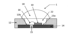
- the semiconductor light emitting device 1 of the present invention includes a reflector 12 having a concave cavity, at least one optical semiconductor element 10 provided on the bottom surface of the concave part, a pad portion 13a for mounting the optical semiconductor element, and an optical A substrate 14 having a lead portion 13b for electrical connection with a semiconductor element is provided.
- the optical semiconductor element mounted on the pad portion is electrically connected to the lead portion by a lead wire 16.
- the cavity may be a gap, but from the viewpoint of preventing electrical problems and protecting the optical semiconductor element from moisture and dust, the optical semiconductor element is sealed and emitted from the optical semiconductor element.
- a resin capable of transmitting light to the outside is filled.
- the sealing resin may contain a substance that converts the wavelength of light, such as a phosphor, if necessary.
- a lens 18 for condensing the light emitted from the optical semiconductor element may be provided on the reflector 12.
- the lens is usually made of a resin, and various structures are adopted depending on the purpose and application, and may be colored as necessary. Hereinafter, each member will be described in detail.
- the substrate 14 in the semiconductor light emitting device 1 of the present invention is a thin metal plate also called a lead frame, and the material used is mainly metal (pure metal, alloy, etc.), for example, aluminum, copper, copper-nickel. -Tin alloys, iron-nickel alloys, etc. Further, the substrate may have a light reflection layer formed so as to cover part or all of the front and back surfaces.
- the light reflection layer desirably has a high reflection function for reflecting light from the optical semiconductor element. Specifically, for electromagnetic waves having a wavelength of 380 nm to 800 nm, the reflectance at each wavelength is preferably 65% to 100%, more preferably 75% to 100%, and more preferably 80% More preferably, it is 100% or less.
- the material of the light reflecting layer include silver and silver-containing alloys.
- the silver content is preferably 60% by mass or more. When the silver content is 60% by mass or more, a sufficient reflection function can be obtained. From the same viewpoint, the silver content is preferably 70% by mass or more, and more preferably 80% by mass or more.
- the thickness of the reflective layer is preferably 1 to 20 ⁇ m. If the thickness of the reflective layer is 1 ⁇ m or more, a sufficient reflection function can be obtained, and if it is 20 ⁇ m or less, it is advantageous in terms of cost and processability is improved.
- the thickness of the substrate is not particularly limited, but is preferably in the range of 0.1 to 1.0 mm.
- the substrate is formed by etching or pressing a metal plate material, and includes a pad portion on which an optical semiconductor element such as an LED chip is mounted and a lead portion that supplies power to the optical semiconductor element.
- the pad portion and the lead portion are insulated, and the optical semiconductor element is connected to the lead portion by a lead wire through processes such as wire bonding and chip bonding.
- the reflector 12 has a function of reflecting the light from the optical semiconductor element in the direction of the light output portion (in the direction of the lens 18 in FIG. 1).
- the reflector according to the present invention is formed of a resin composition containing an inorganic substance, and the diffraction angle 2 ⁇ is 0 degree in the spectrum measured by the X-ray diffraction method using the CuK ⁇ ray (wavelength 1.5418A).
- the intensity ratio (P1) of the peak intensity P1 of the diffraction peak having the maximum intensity and the peak intensity P2 of the diffraction peak having the maximum intensity in the range of the diffraction angle 2 ⁇ of more than 24 degrees to 70 degrees in the range of 24 to 24 degrees. / P2) is 0.01 or more and 1.0 or less, and the ash content is 60% by mass or more.
- the resin composition contains a site where the molecular chains of the resin are regularly arranged (crystallized).
- crystalline resins such as polyethylene, polypropylene, polymethylpentene, polyethylene oxide, polyamide, polyacetal, polyethylene terephthalate, and polyphenylene sulfide, and cross-linked products thereof.
- resin composition containing a crystallized site By using a resin composition containing a crystallized site, a reflector excellent in fatigue resistance, chemical resistance, and mechanical properties can be obtained.
- resin composition which forms the reflector of this invention resin which has the site
- other resins including an amorphous resin may be contained as a mixture.
- Examples of the resin that is easily crystallized include hydrocarbon resins.
- One of the degrees is the diffraction peak with the maximum intensity.
- 2 ⁇ 9.3 ⁇ 1 degree, 13.4 ⁇ 1 degree, 16.7 ⁇ 1 degree, or 18.3 ⁇ 1 degree has a diffraction peak with the maximum intensity.
- a resin having the above diffraction peak that is, a hydrocarbon-based resin, improves moldability and resistance to light.
- the crystallized resin contained in the resin composition forming the reflector of the present invention is not particularly limited, but the intensity is the maximum among the diffraction peaks in the range of 2 ⁇ ranging from 0 degree to 24 degrees.
- the resin composition containing polymethylpentene is excellent in moldability, workability, and heat resistance, and has high transparency, so that even when mixed, it can suppress inhibition of optical properties such as transmittance and reflectance. Is possible.
- the polymethylpentene contained in the resin composition forming the reflector may be a homopolymer of 4-methylpentene-1 or a 4-methylpentene-1 and other ⁇ -olefins such as ethylene and propylene having 2 to 2 carbon atoms. It may be a copolymer with 20 ⁇ -olefins. Furthermore, the polymethylpentene may be a crosslinked product.
- the diffraction peak in the range of 2 ⁇ exceeding 24 degrees to 70 degrees forms the reflector of the present invention. It originates in the inorganic substance contained in the resin composition.
- the inorganic substance contained in the resin composition forming the reflector of the present invention is not particularly limited, but the diffraction having the maximum intensity among the diffraction peaks in the range of 2 ⁇ exceeding 24 degrees to 70 degrees.
- Peaks 2 ⁇ 27.4 ⁇ 1 degree, 36.1 ⁇ 1 degree, 41.2 ⁇ 1 degree, 54.3 ⁇ 1 degree, 56.6 ⁇ 1 degree, 69.0 ⁇ 1 degree, 25.3 ⁇ 1 degree, 37.9 ⁇ 1 degree, 48.1 ⁇ 1 degree, 54.0 ⁇ 1 degree, 55.1 ⁇ 1 degree, 62.7 ⁇ 1 degree, 25.3 ⁇ 1 degree, 25.7 ⁇ 1 30.8 ⁇ 1 degree, 36.3 ⁇ 1 degree, 48.0 ⁇ 1 degree, 54.2 ⁇ 1 degree, or 55.2 ⁇ 1 degree, preferably (1) It is more preferable to have any combination of (3) to (3).
- a diffraction peak of at least 2 ⁇ 27.4 ⁇ 1 degree, 36.1 ⁇ 1 degree, 41.2 ⁇ 1 degree, 54.3 ⁇ 1 degree, 56.6 ⁇ 1 degree, 69.0 ⁇ 1 degree
- at least 2 ⁇ 25.3 ⁇ 1 degree, 37.9 ⁇ 1 degree, 48.1 ⁇ 1 degree, 54.0 ⁇ 1 degree, 55.1 ⁇ 1 degree, 62.7 ⁇ 1 degree
- Combination of diffraction peaks (3)
- At least 2 ⁇ 25.3 ⁇ 1 degree, 25.7 ⁇ 1 degree, 30.8 ⁇ 1 degree, 36.3 ⁇ 1 degree, 48.0 ⁇ 1 degree, 54.2 ⁇ 1 Degree, 55.2 ⁇ 1 degree diffraction peak combination
- the peaks are attributed to the (110) plane, (101) plane, (111) plane, (211) plane, (220) plane, and (301) plane of the rutile crystal of titanium oxide, respectively.
- 2 ⁇ 25.3 ⁇ 1 degree, 37.9 ⁇ 1 degree, 48.1 ⁇ 1 degree, 54.0 ⁇ 1 degree, 55.1 ⁇ 1 degree, 62.7 ⁇ 1 degree
- 2 ⁇ 25.3 ⁇ 1 degree, 25.7 ⁇ 1 degree, 30.8 ⁇ 1 degree, 36.3 ⁇ 1 degree, 48.0 ⁇ 1 degree, and 54.2 ⁇ 1 degree in the above (3).
- 55.2 ⁇ 1 degree diffraction peaks are respectively (120) plane, (111) plane, (121) plane, (012) plane, (231) plane, (320) plane of titanium oxide brookite-type crystal, (241) plane.
- the peak intensity ratio (P1 / P2) is 0.01 or more and 1.0 or less. If the peak intensity ratio (P1 / P2) is less than 0.01, the reflector becomes brittle, and if it exceeds 1.0, sufficient dimensional stability cannot be obtained. From the above viewpoint, the peak intensity ratio (P1 / P2) is preferably in the range of 0.05 or more and 0.75 or less, and more preferably in the range of 0.1 or more and 0.5 or less.
- the average particle size of the titanium oxide contained in the resin composition forming the reflector of the present invention is 0.05 to 0.50 ⁇ m in terms of primary particle size in consideration of moldability and high reflectivity. Is more preferably 0.10 to 0.40 ⁇ m, and further preferably 0.15 to 0.30 ⁇ m.
- the average particle diameter of titanium oxide can be calculated
- the diffraction peak intensity ratio (P1 / P2) of the reflector of the present invention can be measured by an X-ray diffractometer.
- the peak intensities P1 and P2 are integrated values of the respective X-ray diffraction peaks.
- X-ray diffraction measurement conditions Radiation source: CuK ⁇ ray (wavelength: 1.5418A) Scanning axis; 2 ⁇ / ⁇ Tube voltage: 45 kV Tube current: 200 mA Slit; slitr 5.0 degrees scan speed; 5.5 degrees / minute scan step; 0.05 degrees
- the reflector of the present invention requires that the ash content is 60% by mass or more.
- the ash content is preferably 70% by mass or more, and more preferably 75% by mass or more.
- the ash content of the reflector of the present invention can be obtained by measuring only the reflector from the semiconductor light emitting device or the optical semiconductor mounting substrate as a measurement sample, and is a method defined as a general method for determining the ash content of a resin composition ( It can be measured according to JIS K 7250-1 (ISO 3451-1)) and a method based thereon or the TG-DTA method. Among these measuring methods, it is preferable to measure by JIS K 7250-1 (ISO 3451-1) and a method based thereon.
- JIS K 7250-1 (ISO 3451-1) and the method based thereon require a very large amount of sample, if a sufficient amount of sample cannot be obtained, the TG-DTA method can be used. Good.
- the measurement conditions for ash are described below.
- (2) TG-DTA method thermogravimetric / differential thermal analyzer (TG-DTA) was used to measure the mass of the sample to be measured. After heating up to 600 ° C. in minutes, the sample is incinerated by heating at 600 ° C. for 30 minutes. The mass after heating with respect to the mass before heating is expressed as a percentage, and the value is defined as ash.
- the weight ratio of all the inorganic substances including the inorganic substance in which the diffraction peak does not appear in the X-ray diffraction method in the resin composition forming the reflector can be known by measuring the ash content.
- a resin composition containing an inorganic substance a reflector having excellent reflectivity, mechanical properties, and dimensional stability can be obtained.
- those having the effect of obtaining high reflectivity include, for example, titanium oxide, zinc sulfide, zinc oxide, barium sulfide, titanium Potassium acid and the like may be mentioned, and these may be contained alone or in combination, but from the viewpoint of obtaining particularly high reflectivity, it is preferable that titanium oxide is contained, and the crystal type thereof is a rutile type. It is more preferable that
- oxides such as silica, hydroxides such as calcium hydroxide, carbonates such as calcium carbonate, sulfates such as barium sulfate, silicates such as talc, mica and wollastonite
- shapes such as a particle shape and a fiber shape, an irregular cross-sectional fiber shape, a shape with a large unevenness difference, and a thin flake shape. These may be contained alone or in combination.
- inorganic substance which can acquire the high mechanical characteristic and dimensional stability contained in the resin composition which forms the reflector of this invention is a silica particle or glass fiber. Is preferable from the viewpoint of transparency and toughness. Although these have the feature that diffraction peaks are difficult to detect in X-ray diffraction measurement, the weight of all inorganic substances including inorganic substances that can detect diffraction peaks in X-ray diffraction measurement by measuring ash content. It can be detected as a ratio.
- a dispersant may be mixed within a range that does not impair the effects of the present invention.
- the dispersant those generally used for a resin composition containing an inorganic substance can be used, and a silane coupling agent is preferred.
- the silane coupling agent has high dispersibility and compatibility of the inorganic substance with respect to the resin, and can impart high mechanical properties and dimensional stability to the reflector.
- silane coupling agent examples include disilazane such as hexamethyldisilazane; cyclic silazane; trimethylsilane, trimethylchlorosilane, dimethyldichlorosilane, methyltrichlorosilane, allyldimethylchlorosilane, trimethoxysilane, benzyldimethylchlorosilane, Methyltrimethoxysilane, methyltriethoxysilane, isobutyltrimethoxysilane, dimethyldimethoxysilane, dimethyldiethoxysilane, trimethylmethoxysilane, hydroxypropyltrimethoxysilane, phenyltrimethoxysilane, n-butyltrimethoxysilane, n-hexadecyl Trimethoxysilane, n-octadecyltrimethoxysilane, vinyltrimethoxysilane, vinyltri
- the resin composition forming the reflector of the present invention may be mixed with a crosslinking agent within a range that does not impair the effects of the present invention.
- the crosslinking agent has a saturated or unsaturated ring structure, and at least one of the atoms forming at least one ring is an allyl group, a methacryl group, an allyl group via a linking group, and a linking group.
- Those having a structure formed by bonding to any allylic substituent of the methacrylic group via The crosslinking agent having such a structure can exhibit excellent electron beam curability and can impart excellent dimensional stability to the reflector, particularly when used in combination with an electron beam curable resin.
- Examples of the saturated or unsaturated ring structure include a cyclo ring, a hetero ring, and an aromatic ring.
- the number of atoms forming the ring structure is preferably 3 to 12, more preferably 5 to 8, and still more preferably a 6-membered ring.
- Examples of the linking group include an ester bond, an ether bond, an alkylene group, and a (hetero) arylene group.
- triallyl isocyanurate methyl diallyl isocyanurate, diallyl monoglycidyl isocyanuric acid, monoallyl diglycidyl isocyanurate, trimethallyl isocyanurate, diallyl ester of orthophthalic acid, diallyl ester of isophthalic acid and the like.
- the molecular weight of the crosslinking agent is preferably 1000 or less, more preferably 500 or less, and even more preferably 300 or less, from the viewpoints of good dispersibility in the resin composition and causing an effective crosslinking reaction. .
- the number of ring structures is preferably 1 to 3, more preferably 1 or 2, and further preferably 1.
- the content of the crosslinking agent is preferably 0.5 to 40 parts by mass with respect to 100 parts by mass of the resin. With this content, good curability can be imparted without bleeding out. From the above viewpoint, the content of the crosslinking agent is more preferably 1 to 30 parts by mass, and particularly preferably 5 to 20 parts by mass.
- the resin composition forming the reflector of the present invention may contain various additives as long as the effects of the present invention are not impaired.
- the resin composition forming the reflector of the present invention can be prepared by mixing a resin, an inorganic substance, a crosslinking agent added as necessary, and other additives in a predetermined ratio.
- a known means such as a two-roll or three-roll, a homogenizer, a planetary mixer, a stirrer such as a twin-screw kneading extruder, a melt kneader such as a polylab system or a lab plast mill, etc. is applied.
- a known means such as a two-roll or three-roll, a homogenizer, a planetary mixer, a stirrer such as a twin-screw kneading extruder, a melt kneader such as a polylab system or a lab plast mill, etc. is applied.
- a stirrer such as a twin-screw kneading extruder, a melt kneader such as
- the shape of the reflector 12 conforms to the shape of the end portion (joint portion) of the lens 18 and is usually a cylindrical shape such as a square shape, a circular shape, or an oval shape, or an annular shape.
- the reflector 12 is a cylindrical body (annular body), and all the end faces of the reflector 12 are in contact with and fixed to the surface of the substrate 14.
- the reflector 12 has a shape having a recessed cavity, and the inner surface of the reflector 12 may be widened upward in a tapered shape in order to increase the directivity of light from the optical semiconductor element 10.
- the reflector 12 can also function as a lens holder when the end portion on the lens 18 side is processed into a shape corresponding to the shape of the lens 18.
- the cylinder temperature is preferably 200 to 400 ° C., more preferably 220 to 320 ° C. from the viewpoint of moldability.
- the mold temperature is preferably 10 to 170 ° C, more preferably 20 to 150 ° C.
- the reflector according to the present invention may be subjected to ionizing radiation irradiation treatment before or after the molding step, and among them, electron beam irradiation treatment is preferable. By performing the electron beam irradiation treatment, the mechanical properties and dimensional stability of the reflector can be improved.
- the cavity of the reflector according to the present invention is preferably sealed with a resin (sealing resin) capable of sealing the optical semiconductor element and transmitting light emitted from the optical semiconductor element to the outside.
- a resin sealing resin
- the lead wire is disconnected from the connection portion with the optical semiconductor element and / or the connection portion with the electrode due to the force applied by direct contact with the lead wire and the vibration or impact applied indirectly. It is possible to prevent electrical problems caused by cutting, cutting, or short-circuiting.
- the optical semiconductor element can be protected from moisture, dust, etc., and the reliability can be maintained for a long time.
- sealing resin is not specifically limited, Silicone resin, epoxy silicone resin, epoxy resin, acrylic resin, polyimide resin, polycarbonate resin, etc. are mentioned. Of these, silicone resins are preferred from the viewpoints of heat resistance, weather resistance, low shrinkage, and discoloration resistance. Furthermore, the sealing resin may contain a substance that converts the wavelength of light, such as a phosphor, as necessary.
- An optical semiconductor device emits radiated light (generally UV or blue light in a white light LED), for example, an active layer made of AlGaAs, AlGaInP, GaP or GaN sandwiched between n-type and p-type cladding layers
- a semiconductor chip (light emitter) having a double heterostructure, for example, has a hexahedral shape with a side length of about 0.5 mm. And in the case of the form of wire bonding mounting, it is connected to the lead part via the lead wire.
- the substrate for mounting an optical semiconductor according to the present invention is suitably used for the semiconductor light emitting device, and includes a substrate 14 and a reflector 12 having a concave cavity.
- the reflector is formed of a resin composition containing an inorganic substance, and in the spectrum measured by the X-ray diffraction method using the CuK ⁇ ray (wavelength 1.5418A), the reflector has a diffraction angle 2 ⁇ .
- the intensity ratio between the peak intensity P1 of the diffraction peak having the maximum intensity in the range of 0 to 24 degrees and the peak intensity P2 of the diffraction peak having the maximum intensity in the range of the diffraction angle 2 ⁇ of more than 24 degrees to 70 degrees. (P1 / P2) is 0.01 or more and 1.0 or less, and the ash content of the reflector is 60% by mass or more.
- a resin composition for forming a reflector on a substrate (metal frame or lead frame) 14 is molded by transfer molding, compression molding, injection molding or the like using a mold having a cavity space of a predetermined shape, A molded body having a plurality of shaped reflectors is obtained. Since a plurality of reflectors can be produced simultaneously, it is efficient and injection molding is a preferred method. The molded body thus obtained may undergo a curing process such as electron beam irradiation as necessary.
- a substrate on which a reflector is placed is an optical semiconductor mounting substrate (FIG. 2A).
- a separately prepared optical semiconductor element 10 such as an LED chip is disposed on the optical semiconductor mounting substrate (FIG. 2B).
- an adhesive or a bonding member may be used to fix the optical semiconductor element 10.
- a lead wire 16 is provided to electrically connect the optical semiconductor element and the lead portion (electrode). In that case, in order to improve the connection of the lead wire, it is preferable to heat at 100 to 250 ° C. for 5 to 20 minutes.
- FIG. 2D a sealing resin is filled in the cavity of the reflector and cured to produce the sealing portion 22.
- the semiconductor light emitting device shown in FIG. 1 is obtained by dividing into pieces by a method such as dicing at the substantially center (dotted line portion) of the reflector.
- the lens 18 can be disposed on the sealing portion 22 as necessary.
- the sealing resin may be cured after the lens 18 is placed in a state where the sealing resin is uncured.
- FIG. 2F shows the semiconductor light emitting device connected to the wiring board 24 and mounted.
- a method for mounting the semiconductor light emitting device on the wiring board is not particularly limited, but it is preferable to use a melted solder.
- solder is provided on a wiring board, a package is placed on the solder, and then heated to 220 to 270 ° C., which is a general solder melting temperature, in a reflow furnace to melt the solder. And mounting the semiconductor light emitting device on the wiring substrate (solder reflow method).
- solder reflow method A well-known thing can be used for the solder used by the method using said solder.
- Production Example 2 In Production Example 1, a resin composition 2 was obtained in the same manner as in Production Example 1 except that the content of TiO 2 was changed to 350 parts by mass and the blending amount of the dispersant was 5 parts by mass. As in Production Example 1, the formulation is shown in Table 1.
- Production Example 3 In Production Example 1, Production Example 1 except that the content of TiO 2 was changed to 200 parts by mass, the amount of dispersant was 5 parts by mass, and the amount of TAIC was 12 parts by mass. Similarly, a resin composition 3 was obtained. As in Production Example 1, the formulation is shown in Table 1.
- Production Example 4 In Production Example 3, the blending amount of IRGANOX1010 (BASF Japan Co., Ltd.), which is an antioxidant, was 1 part by mass, and 0.5 part by mass of IRGAFOS168 (BASF Japan Co., Ltd.) was blended. A resin composition 4 was obtained in the same manner as in Production Example 3 except that 1 part by mass of KBM-303 (manufactured by Shin-Etsu Silicone Co., Ltd.) was added as a dispersant. As in Production Example 1, the formulation is shown in Table 1.
- Production Example 5 In Production Example 1, a resin composition 5 was obtained in the same manner as in Production Example 1 except that the amount of TAIC was 18 parts by mass. As in Production Example 1, the formulation is shown in Table 1.
- Production Example 6 In Production Example 5, instead of PF70E-001 as a glass fiber, SS05DE-413SP (manufactured by Nitto Boseki Co., Ltd., average fiber length 100 ⁇ m, average fiber diameter 6 ⁇ m) was used except that 120 parts by mass was blended. Thus, a resin composition 6 was obtained. As in Production Example 1, the formulation is shown in Table 1.
- Production Example 7 In Production Example 6, the same procedure as in Production Example 6 was used except that polymethylpentene TPX MX002 (manufactured by Mitsui Chemicals, Inc., weight average molecular weight 500,000 to 700,000) was used as the resin instead of polymethylpentene TPX RT18. Thus, a resin composition 7 was obtained. As in Production Example 1, the formulation is shown in Table 1.
- Production Example 8 In Production Example 5, the same procedure as in Production Example 5 was used except that polymethylpentene TPX DX820 (manufactured by Mitsui Chemicals, Inc., weight average molecular weight 150,000 to 350,000) was used instead of polymethylpentene TPX RT18 as the resin. Thus, a resin composition 8 was obtained. As in Production Example 1, the formulation is shown in Table 1.
- Production Example 9 In Production Example 5, the same procedure as in Production Example 5 was used except that polymethylpentene TPX DX231 (Mitsui Chemicals, Inc., weight average molecular weight 200,000 to 400,000) was used instead of polymethylpentene TPX RT18 as the resin. Thus, a resin composition 9 was obtained.
- the formulation is shown in Table 2.
- Production Example 10 In Production Example 5, a resin composition 10 was obtained in the same manner as in Production Example 5 except that polyethylene hyzex 1300J (manufactured by Prime Polymer Co., Ltd.) was used instead of polymethylpentene TPX RT18 as the resin. The formulation is shown in Table 2 in the same manner as in Production Example 9.
- Production Example 11 In Production Example 5, a resin composition 11 was obtained in the same manner as in Production Example 5 except that polypropylene prime polypro J137G (manufactured by Prime Polymer Co., Ltd.) was used instead of polymethylpentene TPX RT18 as the resin. As in Production Example 9, the formulation is shown in Table 2.
- Comparative production example 1 In Production Example 4, Comparative Resin Composition 1 was obtained in the same manner as Production Example 4 except that no glass fiber was added. As in Production Example 9, the formulation is shown in Table 2.
- Comparative production example 2 In Production Example 4, the comparative resin composition 2 was prepared in the same manner as in Production Example 4 except that the blending amount of TiO 2 was 100 parts by mass, the TAIC content was 4 parts by mass, and no glass fiber was blended. Obtained. As in Production Example 9, the formulation is shown in Table 2.
- Comparative production example 3 In Production Example 4, the compounding amount of TiO 2 was 45 parts by mass, the TAIC content was 4 parts by mass, and the glass fiber was CSG3PA-820 (manufactured by Nitto Boseki Co., Ltd., average fiber length 3 mm, modified) Comparative resin composition 3 was obtained in the same manner as in Production Example 4 except that 60 parts by mass of ratio 4) was blended. As in Production Example 9, the formulation is shown in Table 2.
- Comparative production example 4 In Production Example 1, a comparative resin composition 4 was obtained in the same manner as in Production Example 1 except that TiO 2 was not blended and the TAIC content was 6 parts by mass. As in Production Example 9, the formulation is shown in Table 2.
- Each of the resin compositions 1 to 11 prepared in Production Examples 1 to 11 is made of copper, which is silver-plated as a light reflecting layer by an injection molding machine TR55EH (manufactured by Sodick Co., Ltd., screw diameter ⁇ 22 mm).
- TR55EH injection molding machine
- a molded body having a plurality of reflectors having outer dimensions: 30 mm ⁇ 30 mm and thickness: 0.35 mm was obtained.
- the injection molding conditions were appropriately set between a cylinder temperature of 220 to 320 ° C. and a mold temperature of 20 to 150 ° C. according to the resin composition.
- Each molded body was irradiated with an electron beam at an acceleration voltage of 800 kV and an absorbed dose of 400 kGy to obtain a substrate for mounting an optical semiconductor.
- Separately prepared LED elements (light emission color: blue) were arranged on the pad portions of the respective optical semiconductor mounting substrates produced as described above, and fixed with an adhesive. The LED element and the lead part were connected with the lead wire and then diced into individual pieces to obtain a semiconductor light emitting device.
- Comparative Examples 1 to 4 Using the comparative resin compositions 1 to 4 prepared in Comparative Production Examples 1 to 4, an optical semiconductor mounting substrate and a semiconductor light emitting device were obtained in the same manner as in the Examples.
- Ash content The measurement sample was obtained by cutting out only the reflector from the substrate for mounting an optical semiconductor produced in each example and comparative example, and the method A (direct ashing method) of JIS K 7250-1 (ISO 3451-1) ), The ash content was measured as follows. First, the crucible was heated to a constant weight in a muffle furnace heated to 800 ° C. (FO310 manufactured by Yamato Scientific Co., Ltd.), and then cooled to room temperature in a desiccator. Subsequently, the mass of the crucible was measured to an order of 0.1 mg with an electronic small balance (AG104 manufactured by METTLER TOLEDO).
- the sample was pre-dried at 60 ° C for 2 to 5 hours with a ventilation constant temperature thermostat (DKM400 manufactured by Yamato Kagaku Co., Ltd.), then transferred to a crucible, and the mass was measured to an order of 0.1 mg with a small electronic balance.
- the mass of the sample before ashing was obtained by subtracting the mass of the crucible from the value.
- the mass of the sample after ashing with respect to the mass of the sample before ashing was expressed as a percentage, and the value was defined as ash.
- the measurement results are shown in Tables 3 and 4.
- the reflectance of the reflector at a wavelength of 230 to 780 nm is measured using a reflectance measuring device MCPD-9800 (manufactured by Otsuka Electronics Co., Ltd.). Measured. Tables 3 and 4 show the results of reflectance at a wavelength of 450 nm.
- the same semiconductor light emitting device was allowed to emit light continuously at a constant current of 200 mA in an environment of a temperature of 85 ° C. and a humidity of 85% RH.
- the luminous flux emitted at a constant current of 200 mA after a cumulative time of 500 hours is measured with an instantaneous multi-photometry system (wide dynamic range type) MCPD-9800 (manufactured by Otsuka Electronics Co., Ltd.), and the luminous flux after 500 hours ( ⁇ 500 ) It was. From the measured initial luminous flux ( ⁇ 0 ) and the luminous flux after 500 hours ( ⁇ 500 ), the luminous flux deterioration rate was calculated according to the following formula A.
- Luminous flux degradation rate (%)
- Tables 3 and 4 show the luminous flux deterioration rates calculated from the initial luminous flux ( ⁇ 0 ) and the luminous flux after 500 hours ( ⁇ 500 ).
- Comparative Examples 1 to 11 since the dimensional stability was 1% or less, the reflectance was 90% or more, and the luminous flux deterioration rate after a high-temperature and high-humidity operation test was 3% or less, good performance as a semiconductor light emitting device was obtained. It was. On the other hand, Comparative Examples 1 to 3 had a dimensional stability of 10% or more and a luminous flux deterioration rate of 10% or more after the high-temperature and high-humidity operation test, so that sufficient performance as a semiconductor light emitting device could not be satisfied. Furthermore, since Comparative Example 4 had a dimensional stability of 10% or more and a reflectance of 46%, the performance sufficient as a semiconductor light emitting device could not be satisfied.
- a semiconductor light emitting device including at least a substrate, a reflector having a concave cavity, and an optical semiconductor element, the reflector is formed of a resin composition containing an inorganic substance, and the reflector is formed of CuK ⁇
- the peak intensity P1 and diffraction angle 2 ⁇ of the diffraction peak having the maximum intensity in the range where the diffraction angle 2 ⁇ is 0 degree to 24 degrees are
- the intensity ratio (P1 / P2) of the peak intensity P2 of the diffraction peak having the maximum intensity in the range of more than 24 degrees to 70 degrees is 0.01 or more and 1.0 or less, and the ash content is 60 mass% or more.
- the present invention it is possible to provide a semiconductor light emitting device and an optical semiconductor mounting substrate in which the reflector has extremely high reflectivity and is excellent in dimensional stability.
- SYMBOLS 1 Semiconductor light-emitting device 10; Semiconductor element 12; Reflector 13a; Pad part 13b; Lead part 14; Substrate (metal frame, lead frame) 15; Insulating part 16; Lead wire 18; Lens 22; Sealing part 24;
Landscapes
- Engineering & Computer Science (AREA)
- Microelectronics & Electronic Packaging (AREA)
- Computer Hardware Design (AREA)
- Power Engineering (AREA)
- Manufacturing & Machinery (AREA)
- Led Device Packages (AREA)
Abstract
Description
このように、リフレクターには耐熱性が要求されることから、耐熱性を改良したリフレクターの開発が進められている。例えば、特許文献1では、(A)エポキシ樹脂、(B)硬化剤、(C)硬化触媒、(D)無機充填剤、(E)白色顔料、および(F)カップリング剤を含有する光反射用熱硬化性樹脂組成物が提案されている。
特許文献2では、1,4-シクロヘキサンジカルボン酸単位を50~100モル%含むジカルボン酸単位と炭素数4~18の脂肪族ジアミン単位を50~100モル%含むジアミン単位とを有するポリアミドを含有するポリアミド組成物が提案されている。
特許文献3では、炭素-水素結合を有するフッ素樹脂(A)及び酸化チタン(B)からなる樹脂組成物が提案されている。また、特許文献4では、特定の架橋処理剤を含む電子線硬化性樹脂組成物なども提案され、該樹脂組成物をリフレクターに用いた半導体発光装置が提案されている。
しかしながら、従来使用されてきた半導体発光装置は耐熱性が十分とは言えず、特に上記の加熱によるリフロー工程においては、部品表面の温度が局部的に高くなり変形が生じる等の問題がある。リフレクターの形状が変化すると光の反射角等も変化してしまうため、LEDパッケージは、設計通りの発光特性を示しにくくなる。また、LEDパッケージの外形寸法が変化し、配線基板との接続に対して不具合を生じる。このため、熱に対する寸法安定性に優れたリフレクターを備えた半導体発光装置が望まれていた。
(1)基板、凹部形状のキャビティを有するリフレクター、及び光半導体素子を少なくとも備えた半導体発光装置であって、該リフレクターが無機物質を含有する樹脂組成物により形成され、該リフレクターを、CuKα線(波長1.5418A)を用いたX線回折法によって測定したスペクトルにおいて、回折角2θが0度から24度の範囲のうち、強度が最大となる回折ピークのピーク強度P1と回折角2θが24度超から70度の範囲で、強度が最大となる回折ピークのピーク強度P2の強度比(P1/P2)が、0.01以上1.0以下であり、かつ該リフレクターの灰分が60質量%以上であることを特徴とする半導体発光装置、及び
(2)基板及び凹部形状のキャビティを有するリフレクターを備えた光半導体実装用基板であって、該リフレクターが無機物質を含有する樹脂組成物により形成され、該リフレクターを、CuKα線(波長1.5418A)を用いたX線回折法によって測定したスペクトルにおいて、回折角2θが0度から24度の範囲のうち、強度が最大となる回折ピークのピーク強度P1と回折角2θが24度超から70度の範囲で、強度が最大となる回折ピークのピーク強度P2の強度比(P1/P2)が、0.01以上1.0以下であり、かつ該リフレクターの灰分が60質量%以上であることを特徴とする光半導体実装用基板を提供するものである。
本発明の半導体発光装置1は、凹部形状のキャビティを有するリフレクター12と、凹部の底面に設けられ、少なくとも1つの光半導体素子10と、該光半導体素子を搭載するためのパッド部13a、及び光半導体素子と電気的に接続するためのリード部13bを有した基板14を備える。パッド部に搭載された光半導体素子は、リード線16によりリード部に電気的に接続されている。
また、キャビティは、空隙であってもよいが、電気的な不具合の防止、光半導体素子の湿気及び塵埃等からの保護の観点から、光半導体素子を封止するとともに光半導体素子から発せられた光を外部に透過させることが可能な樹脂(封止樹脂)が充填されていることが好ましい。該封止樹脂は、必要に応じて蛍光体などの光の波長を変換する物質が含有されていてもよい。さらに、光半導体素子から発せられた光を集光させるためのレンズ18をリフレクター12の上に設けてもよい。該レンズは、通常樹脂製であり、目的、用途等により様々な構造が採用され、必要に応じて着色されていてもよい。
以下、各部材について、詳細に説明する。
本発明の半導体発光装置1における基板14は、リードフレームとも称される金属製の薄板であり、用いられる材料としては主に金属(純金属や合金など)、例えば、アルミニウム、銅、銅-ニッケル-スズの合金、鉄-ニッケルの合金などが挙げられる。また基板は、表裏面の一部、または全部を覆うように光反射層が形成されていてもよい。光反射層は、光半導体素子からの光を反射する反射機能が高いことが望ましい。具体的には、380nm以上800nm以下の波長の電磁波に対して、各波長における反射率が65%以上100%以下であることが好ましく、75%以上100%以下であることがより好ましく、80%以上100%以下であることがさらに好ましい。反射率が高いとLED素子が発する光のロスが小さく、LEDパッケージとしての発光効率が高くなる。
光反射層の材質としては例えば銀や銀を含有する合金を挙げることができるが、銀の含有率は60質量%以上であることが好ましい。銀の含有率が60質量%以上であると、十分な反射機能が得られる。同様の観点から、銀の含有率は70質量%以上がより好ましく、80質量%以上がさらに好ましい。
なお反射層の厚みは1~20μmが望ましい。反射層の厚みが1μm以上であると十分な反射機能が得られ、20μm以下であればコスト的に有利であるとともに、加工性が向上する。
基板は、金属製の板材をエッチングやプレス加工などの工程を経て形成され、LEDチップ等の光半導体素子を搭載するパッド部と該光半導体素子に電力を供給するリード部を有する。パッド部とリード部は絶縁されており、光半導体素子はワイヤーボンディングやチップボンディングなどの工程を経て、リード線によりリード部と接続される。
リフレクター12は、光半導体素子からの光を出光部の方向(図1においては、レンズ18の方向)に反射させる作用を有する。
本発明に係るリフレクターは、無機物質を含有する樹脂組成物により形成され、該リフレクターを、CuKα線(波長1.5418A)を用いたX線回折法によって測定したスペクトルにおいて、回折角2θが0度から24度の範囲のうち、強度が最大となる回折ピークのピーク強度P1と回折角2θが24度超から70度の範囲で、強度が最大となる回折ピークのピーク強度P2の強度比(P1/P2)が、0.01以上1.0以下であり、かつ灰分が60質量%以上であることを特徴とする。
結晶化した部位を含有する樹脂組成物を用いることで、耐疲労性、耐薬品性、機械的特性に優れたリフレクターを得ることができる。本発明のリフレクターを形成する樹脂組成物としては、結晶化した部位を有する樹脂が単独で含有されていてもよいし、結晶化した部位を有する樹脂が複数含まれる混合物となっていてもよい。さらに、本願発明の効果を阻害しない範囲で結晶化した部位を含む樹脂の他に、非結晶性の樹脂を含むそれ以外の樹脂が混合物として含有されていてもよい。
結晶化した部位が含有されている樹脂のなかでも、上記回折ピークを有する樹脂、すなわち炭化水素系樹脂であると、成形加工性や、光に対する耐性が向上する。
リフレクターを形成する樹脂組成物に含まれるポリメチルペンテンとしては4-メチルペンテン-1の単独重合体でも、4-メチルペンテン-1と他のα-オレフィン、例えばエチレン、プロピレン等の炭素数2~20のα-オレフィンとの共重合体でもよい。さらに、前記ポリメチルペンテンは、架橋体であってもよい。
本発明のリフレクターを形成する樹脂組成物に含まれる無機物質としては、特に限定されるものではないが、前記2θが24度超から70度の範囲の回折ピークのうち、強度が最大となる回折ピークが2θ=27.4±1度、36.1±1度、41.2±1度、54.3±1度、56.6±1度、69.0±1度、25.3±1度、37.9±1度、48.1±1度、54.0±1度、55.1±1度、62.7±1度、25.3±1度、25.7±1度、30.8±1度、36.3±1度、48.0±1度、54.2±1度、55.2±1度のいずれかであることが好ましく、次の(1)~(3)のいずれかの組み合わせを有することがより好ましい。
(1)少なくとも2θ=27.4±1度、36.1±1度、41.2±1度、54.3±1度、56.6±1度、69.0±1度の回折ピークの組み合わせ
(2)少なくとも2θ=25.3±1度、37.9±1度、48.1±1度、54.0±1度、55.1±1度、62.7±1度の回折ピークの組み合わせ
(3)少なくとも2θ=25.3±1度、25.7±1度、30.8±1度、36.3±1度、48.0±1度、54.2±1度、55.2±1度の回折ピークの組み合わせ
また、ルチル型の場合は、2θ=27.4±1度に最大強度の回折ピークがあり、アナターゼ型およびブルッカイト型の場合は、2θ=25.3±1度に最大強度の回折ピークがある。
これらのうち、リフレクターを形成する樹脂組成物に無機物質として含まれる酸化チタンの結晶型はルチル型であることが、熱安定性が高い上に、特に高い反射性が得られるため好ましい。すなわち、酸化チタンに由来する回折ピークのうち最大強度の回折ピークはルチル型結晶の(110)面に帰属される2θ=27.4±1度の回折ピークであることが好ましい。
本発明のリフレクターの回折ピーク強度比(P1/P2)はX線回折装置により測定することができる。測定試料形態としては、本発明の半導体発光装置または光半導体実装用基板からリフレクターのみを切り出すか、あるいは半導体発光装置または光半導体実装用基板をそのまま使用することができ、これを試料台の上に置き、下記の条件でX線回折測定を行う。このとき、非晶ハローピークの影響を排除するため、得られたスペクトルのうち半値幅が2θ=6度以下となる波形を回折ピークと定義する。また、ピーク強度P1及びP2は、各X線回折ピークの積分値とする。
X線回折測定条件
線源;CuKα線(波長;1.5418A)
走査軸;2θ/θ
管電圧;45kV
管電流;200mA
スリット;soller slit 5.0度
スキャンスピード;5.5度/分
スキャンステップ;0.05度
本発明のリフレクターの灰分は、半導体発光装置または光半導体実装用基板からリフレクターのみを切り出したものを測定試料とすることができ、一般的な樹脂組成物の灰分の求め方として規定された方法(JIS K 7250-1(ISO 3451-1))及びそれに準拠した方法、あるいはTG-DTA法に従って測定することができる。これらの測定方法の内、JIS K 7250-1(ISO 3451-1)及びそれに準拠した方法で測定することが好ましい。ただし、JIS K 7250-1(ISO 3451-1)及びそれに準拠した方法は非常に多くの試料量が必要であるため、十分な試料量が得られない場合はTG-DTA法で測定してもよい。
以下に灰分の測定条件を記す。
(1)JIS K 7250-1(ISO 3451-1)
A法(直接灰化法)
灰化温度;800℃
灰化時間;2時間
(2)TG-DTA法
熱重量/示差熱同時分析装置(TG-DTA)を用いて、測定試料の質量を測定した後、アルミパン中、大気雰囲気下、10℃/分で600℃まで昇温後、そのまま600℃で30分間加熱し試料を灰化する。加熱前の質量に対する加熱後の質量を百分率で表し、その値を灰分とする。
本発明のリフレクターを形成する樹脂組成物に含有される無機物質の中で、高い反射性を得ることができる効果を有するものとしては、例えば、酸化チタン、硫化亜鉛、酸化亜鉛、硫化バリウム、チタン酸カリウムなどが挙げられ、これらは単独または混合されて含有されていてもよいが、特に高い反射性を得られるという観点から、酸化チタンが含有されていることが好ましく、その結晶型はルチル型であることがより好ましい。
これらは単独または混合されて含有されていてもよい。本発明のリフレクターを形成する樹脂組成物に含有される、高い機械的特性及び寸法安定性を得ることができる無機物質としては、特に限定されるものではないが、シリカ粒子またはガラス繊維であることが透明性、強靭性等の点から好ましい。
なお、これらはX線回折測定において回折ピークが検出されにくいという特徴を持つが、灰分の測定をすることで、X線回折測定において回折ピークが検出できる無機物質を含めた全ての無機物質の重量比として検出することができる。
本発明のリフレクターを形成する樹脂組成物は、上記材料に加えて、本願発明の効果を阻害しない範囲で分散剤が混合されていてもよい。分散剤としては、一般的に無機物質を含有する樹脂組成物に用いられるものを使用することができるが、シランカップリング剤が好ましい。シランカップリング剤は樹脂に対する無機物質の分散性、相溶性が高く、リフレクターに高い機械的特性、寸法安定性を付与することができる。
シランカップリング剤としては、例えば、ヘキサメチルジシラザン等のジシラザン;環状シラザン;トリメチルシラン、トリメチルクロルシラン、ジメチルジクロルシラン、メチルトリクロルシラン、アリルジメチルクロルシラン、トリメトキシシラン、ベンジルジメチルクロルシラン、メチルトリメトキシシラン、メチルトリエトキシシラン、イソブチルトリメトキシシラン、ジメチルジメトキシシラン、ジメチルジエトキシシラン、トリメチルメトキシシラン、ヒドロキシプロピルトリメトキシシラン、フェニルトリメトキシシラン、n-ブチルトリメトキシシラン、n-ヘキサデシルトリメトキシシラン、n-オクタデシルトリメトキシシラン、ビニルトリメトキシシラン、ビニルトリエトキシシラン、プロペニルトリメトキシシラン、プロペニルトリエトキシシラン、ブテニルトリメトキシシラン、ブテニルトリエトキシシラン、ペンテニルトリメトキシシラン、ペンテニルトリエトキシシラン、ヘキセニルトリメトキシシラン、ヘキセニルトリエトキシシラン、ヘプテニルトリメトキシシラン、ヘプテニルトリエトキシシラン、オクテニルトリメトキシシラン、オクテニルトリエトキシシラン、ノネニルトリメトキシシラン、ノネニルトリエトキシシラン、デケニルトリメトキシシラン、デケニルトリエトキシシラン、ウンデケニルトリメトキシシラン、ウンデケニルトリエトキシシラン、ドデケニルトリメトキシシラン、ドデケニルトリエトキシシラン、γ-メタクリルオキシプロピルトリメトキシシラン、及びビニルトリアセトキシシラン等のアルキルシラン化合物;γ-アミノプロピルトリエトキシシラン、γ-(2-アミノエチル)アミノプロピルトリメトキシシラン、γ-(2-アミノエチル)アミノプロピルメチルジメトキシシラン、N-フェニル-3-アミノプロピルトリメトキシシラン、N-(2-アミノエチル)3-アミノプロピルトリメトキシシラン、及びN-β-(N-ビニルベンジルアミノエチル)-γ-アミノプロピルトリメトキシシラン、ヘキシルトリメトキシシラン等のアミノシラン化合物;等が挙げられる。
本発明のリフレクターを形成する樹脂組成物は、上記材料に加えて、本願発明の効果を阻害しない範囲で架橋処理剤が混合されていてもよい。架橋処理剤としては、飽和もしくは不飽和の環構造を有し、少なくとも1つの環を形成する原子のうち少なくとも1つの原子が、アリル基、メタクリル基、連結基を介したアリル基、及び連結基を介したメタクリル基のいずれかのアリル系置換基と結合してなる構造を有するものが好ましい。
かかる構造を有する架橋処理剤は、特に電子線硬化性樹脂と併用することで、良好な電子線硬化性を発揮し、リフレクターに優れた寸法安定性を付与することができる。
より具体的には、トリアリルイソシアヌレート、メチルジアリルイソシアヌレート、ジアリルモノグリシジルイソシアヌル酸、モノアリルジグリシジルイソシアヌレート、トリメタリルイソシアヌレート、オルトフタル酸のジアリルエステル、イソフタル酸のジアリルエステル等が挙げられる。
また、架橋処理剤の含有量は、樹脂100質量部に対して、0.5~40質量部であることが好ましい。この含有量であると、ブリードアウトすることなく、かつ良好な硬化性を付与することができる。以上の観点から、架橋処理剤の含有量は1~30質量部であることがさらに好ましく、5~20質量部であることが特に好ましい。
本発明のリフレクターを形成する樹脂組成物は、上記材料に加えて、本願発明の効果を阻害しない範囲で種々の添加剤が含有されていてもよい。例えば、樹脂組成物の性質を改善する目的で、種々のウィスカー、シリコーンパウダー、熱可塑性エラストマー、有機合成ゴム、脂肪酸エステル、グリセリン酸エステル、ステアリン酸亜鉛、ステアリン酸カルシウム等の内部離型剤や、ベンゾフェノン系、サリチル酸系、シアノアクリレート系、イソシアヌレート系、シュウ酸アニリド系、ベンゾエート系、ヒンダードアミン系、ベンゾトリアゾール系、フェノール系等の酸化防止剤や、ヒンダードアミン系、ベンゾエート系等の光安定剤といった添加剤を配合することができる。
本発明のリフレクターを形成する樹脂組成物は、樹脂、無機物質、及び必要に応じて添加される架橋処理剤、その他の添加剤を所定比で混合して作製することができる。混合方法としては、2本ロールあるいは3本ロール、ホモジナイザー、プラネタリーミキサー、2軸混練押出機等の撹拌機、ポリラボシステムやラボプラストミル等の溶融混練機等の公知の手段を適用することができる。これらは常温、冷却状態、加熱状態、常圧、減圧状態、加圧状態のいずれで行ってもよい。
リフレクター12の形状は、レンズ18の端部(接合部)の形状に準じており、通常、角形、円形、楕円形等の筒状又は輪状である。図1の概略断面図においては、リフレクター12は、筒状体(輪状体)であり、リフレクター12のすべての端面が基板14の表面に接触、固定されている。
また、リフレクター12は、凹部形状のキャビティを有する形状であり、リフレクター12の内面は、光半導体素子10からの光の指向性を高めるために、テーパー状に上方に広げられていてもよい。
また、リフレクター12は、レンズ18側の端部を、当該レンズ18の形状に応じた形に加工された場合には、レンズホルダーとしても機能させることができる。
本発明に係るリフレクターの製造方法としては、特に限定されるものではないが、上記樹脂組成物を用いた射出成形による製造が好ましい。このとき、成形性の観点から、シリンダー温度は200~400℃が好ましく、220~320℃がより好ましい。また、金型温度は10~170℃が好ましく、20~150℃がより好ましい。
本発明に係るリフレクターは、さらに必要に応じて、成形工程の前又は後に、電離放射線照射処理を施しても良く、なかでも、電子線照射処理が好ましい。電子線照射処理を施すことによって、リフレクターの機械的特性、寸法安定性を向上させることができる。
本発明に係るリフレクターのキャビティは、光半導体素子を封止するとともに光半導体素子から発せられた光を外部に透過させることが可能な樹脂(封止樹脂)で封止されていることが好ましい。ワイヤーボンディング実装において、リード線に直接接触することにより加わる力、及び、間接的に加わる振動、衝撃等により、光半導体素子との接続部、及び/又は、電極との接続部からリード線が外れたり、切断したり、短絡したりすることによって生じる電気的な不具合を防止することができる。また、同時に、湿気、塵埃等から光半導体素子を保護し、長期間に渡って信頼性を維持することができる。
封止樹脂として用いられるものとしては、特に限定されるものではないが、シリコーン樹脂、エポキシシリコーン樹脂、エポキシ系樹脂、アクリル系樹脂、ポリイミド系樹脂、ポリカーボネート樹脂等が挙げられる。これらのうち、耐熱性、耐候性、低収縮性及び耐変色性の観点から、シリコーン樹脂が好ましい。さらに該封止樹脂は、必要に応じて蛍光体などの光の波長を変換する物質が含有されていてもよい。
光半導体素子は、放射光(一般に、白色光LEDにおいてはUV又は青色光)を放出する、例えば、AlGaAs、AlGaInP、GaP又はGaNからなる活性層を、n型及びp型のクラッド層により挟んだダブルヘテロ構造を有する半導体チップ(発光体)であり、例えば、一辺の長さが0.5mm程度の六面体の形状をしている。そして、ワイヤーボンディング実装の形態の場合には、リード線を介してリード部に接続されている。
本願発明の光半導体実装用基板は、上記半導体発光装置に好適に用いられ、基板14及び凹部形状のキャビティを有するリフレクター12を備える。該リフレクターは、上述のように、無機物質を含有する樹脂組成物により形成され、該リフレクターを、CuKα線(波長1.5418A)を用いたX線回折法によって測定したスペクトルにおいて、回折角2θが0度から24度の範囲の中で強度が最大となる回折ピークのピーク強度P1と、回折角2θが24度超から70度の範囲で強度が最大となる回折ピークのピーク強度P2の強度比(P1/P2)が、0.01以上1.0以下であり、かつ該リフレクターの灰分が60質量%以上であることを特徴とする。
本発明の光半導体実装用基板の製造方法の一例について、図2を参照しつつ説明するが、本発明の光半導体実装用基板の製造方法は、この例によってなんら限定されるものではない。
まず、基板(金属フレーム又はリードフレーム)14上にリフレクターを形成するための樹脂組成物を、所定形状のキャビティ空間を備える金型を用いたトランスファー成形、圧縮成形、射出成形等により成形し、所定形状のリフレクターを複数有する成形体を得る。リフレクターを複数個、同時に作製することができるので効率的であり、射出成形が好ましい手法である。このようにして得た成形体は必要に応じて電子線照射等の硬化過程を経てもよい。この段階、すなわち基板上にリフレクターを載置したものが光半導体実装用基板(図2(a))である。
続いて、本発明の半導体発光装置の製造方法の一例について、図2を参照しつつ説明するが、本発明の半導体発光装置の製造方法は、この例によってなんら限定されるものではない。
上記光半導体実装用基板に、別途、準備したLEDチップ等の光半導体素子10を配置する(図2(b))。この際、光半導体素子10を固定するために、接着剤や接合部材を用いてもよい。
次に、図2(c)に示すように、リード線16を設けて、光半導体素子とリード部(電極)を電気的に接続する。その際には、リード線の接続を良好にするために、100~250℃で5~20分間加熱することが好ましい。
次に、図2(e)に示すように、リフレクターのほぼ中央(点線部)で、ダイシングなどの方法で個片化し、図1に示す半導体発光装置を得る。必要に応じて、封止部22上にレンズ18を配設することができる。なおその場合は、封止樹脂が未硬化の状態でレンズ18を載置してから、封止樹脂を硬化させてもよい。
該半導体発光装置を配線基板24上に接続し、実装したものが図2(f)である。半導体発光装置を配線基板上に実装する方法は、特に限定されるものではないが、溶融させた半田を用いて行うことが好ましい。より具体的には、配線基板上に半田を設けておき、その半田上にパッケージを載せてから、リフロー炉により一般的な半田の溶融温度である220~270℃に加熱して、半田を溶融させて配線基板上に半導体発光装置を実装する方法(半田リフロー法)である。上記の半田を用いる方法で使用する半田は、周知のものが使用できる。
製造例1
ポリメチルペンテン TPX RT18(三井化学(株)製、重量平均分子量50万~70万)100質量部に対して、無機物質として、酸化チタン PF-691(石原産業(株)製、ルチル型、平均粒径0.21μm、以下「TiO2」と記載する。)450質量部、ガラス繊維 PF70E-001(日東紡績(株)製、平均繊維長70μm、平均繊維径10μm)120質量部、架橋処理剤として、トリアリルイソシアネート(日本化成(株)製、分子量249.3、以下「TAIC」と記載する。)20質量部、酸化防止剤としてIRGANOX1010(BASF・ジャパン(株)製)5質量部、PEP-36((株)ADEKA製)0.5質量部、離型剤としてSZ-2000(堺化学(株)製)0.5質量部、分散剤としてKBM-3063(信越シリコーン(株)製)7質量部を配合、混練し、樹脂組成物1を得た。なお、混練はポリラボシステム(バッチ式2軸)で行った。配合を表1に記す。
製造例1において、TiO2の含有量を350質量部に変更したこと、及び分散剤の配合量を5質量部としたこと以外は製造例1と同様にして樹脂組成物2を得た。製造例1と同様に、配合を表1に記す。
製造例1において、TiO2の含有量を200質量部に変更したこと、分散剤の配合量を5質量部としたこと、及びTAICの配合量を12質量部としたこと以外は製造例1と同様にして樹脂組成物3を得た。製造例1と同様に、配合を表1に記す。
製造例3において、酸化防止剤であるIRGANOX1010(BASF・ジャパン(株)製)の配合量を1質量部とし、さらにIRGAFOS168(BASF・ジャパン(株)製)を0.5質量部配合したこと、及び分散剤としてKBM-303(信越シリコーン(株)製)を1質量部配合したこと以外は製造例3と同様にして樹脂組成物4を得た。製造例1と同様に、配合を表1に記す。
製造例1において、TAICの配合量を18質量部としたこと以外は製造例1と同様にして樹脂組成物5を得た。製造例1と同様に、配合を表1に記す。
製造例5において、ガラス繊維としてPF70E-001に代えて、SS05DE-413SP(日東紡績(株)製、平均繊維長100μm、平均繊維径6μm)を120質量部配合したこと以外は製造例5と同様にして樹脂組成物6を得た。製造例1と同様に、配合を表1に記す。
製造例6において、樹脂としてポリメチルペンテン TPX RT18に代えて、ポリメチルペンテン TPX MX002(三井化学(株)製、重量平均分子量50万~70万)を用いたこと以外は製造例6と同様にして樹脂組成物7を得た。製造例1と同様に、配合を表1に記す。
製造例5において、樹脂としてポリメチルペンテン TPX RT18に代えて、ポリメチルペンテン TPX DX820(三井化学(株)製、重量平均分子量15万~35万)を用いたこと以外は製造例5と同様にして樹脂組成物8を得た。製造例1と同様に、配合を表1に記す。
製造例5において、樹脂としてポリメチルペンテン TPX RT18に代えて、ポリメチルペンテン TPX DX231(三井化学(株)製、重量平均分子量20万~40万)を用いたこと以外は製造例5と同様にして樹脂組成物9を得た。配合を表2に記す。
製造例5において、樹脂としてポリメチルペンテン TPX RT18に代えて、ポリエチレン ハイゼックス 1300J((株)プライムポリマー製)を用いたこと以外は製造例5と同様にして樹脂組成物10を得た。製造例9と同様に、配合を表2記す。
製造例5において、樹脂としてポリメチルペンテン TPX RT18に代えて、ポリプロピレン プライムポリプロ J137G((株)プライムポリマー製)を用いたこと以外は製造例5と同様にして樹脂組成物11を得た。製造例9と同様に、配合を表2に記す。
製造例4において、ガラス繊維を配合しなかったこと以外は製造例4と同様にして比較樹脂組成物1を得た。製造例9と同様に、配合を表2に記す。
製造例4において、TiO2の配合量を100質量部とし、TAICの含有量を4質量部とし、かつガラス繊維を配合しなかったこと以外は製造例4と同様にして比較樹脂組成物2を得た。製造例9と同様に、配合を表2に記す。
製造例4において、TiO2の配合量を45質量部とし、TAICの含有量を4質量部とし、かつガラス繊維として、ガラス繊維CSG3PA-820(日東紡績(株)製、平均繊維長3mm、異形比4)を60質量部配合したこと以外は製造例4と同様にして比較樹脂組成物3を得た。製造例9と同様に、配合を表2に記す。
製造例1において、TiO2を配合せず、またTAICの含有量を6質量部としたこと以外は製造例1と同様にして比較樹脂組成物4を得た。製造例9と同様に、配合を表2に記す。
製造例1~11にて調製した樹脂組成物1~11を用いて、それぞれ射出成形機TR55EH((株)ソディック製、スクリュー径φ22mm)により、光反射層として銀メッキを施した、銅からなる基板(リードフレーム)(75mm×62mm×0.25mm)上に外形寸法:30mm×30mm、厚み:0.35mmとなるようなリフレクターを複数有する成形体を得た。射出成形の条件はシリンダー温度220~320℃、金型温度20~150℃の間で、樹脂組成物に応じてそれぞれ適宜設定した。各成形体について、加速電圧800kV、吸収線量400kGyにて電子線を照射し、光半導体実装用基板を得た。
上記により作製した各光半導体実装用基板のパッド部に、それぞれ別途準備したLED素子(発光色:青)を配置し、接着剤により固定した。リード線により、LED素子とリード部を接続した後ダイシングして個片化し、半導体発光装置を得た。
比較製造例1~4にて調製した比較樹脂組成物1~4を用いて、実施例と同様にして光半導体実装用基板及び半導体発光装置を得た。
(1)回折ピーク強度比(P1/P2)
各実施例及び比較例にて作製した光半導体実装用基板をX線回折装置の試料台の上に置き、下記の条件でX線回折測定を行った。測定結果を表3及び表4に示す。
X線回折測定条件
装置名;Smart Lab((株)リガク製)
線源;CuKα線(波長;1.5418A)
走査軸;2θ/θ
管電圧;45kV
管電流;200mA
スリット;soller slit 5.0度
スキャンスピード;5.5度/分
スキャンステップ;0.05度
各実施例及び比較例にて作製した光半導体実装用基板からリフレクターのみを切り出したものを測定試料とし、JIS K 7250-1(ISO 3451-1)のA法(直接灰化法)に基づいて下記の通り灰分を測定した。
まず、800℃に加熱されたマッフル炉(FO310 ヤマト科学(株)製)で、恒量になるまでるつぼを加熱した後、デシケータ中で室温になるまで冷却した。次いで、電子小型天秤(AG104 メトラー・トレド(株)製)で0.1mgの桁までるつぼの質量を測定した。次に試料を送風定温恒温器(DKM400 ヤマト科学(株)製)で60℃2~5時間予備乾燥した後、るつぼに全量を移して電子小型天秤で0.1 mgの桁まで質量を測定し、その値からるつぼの質量を差し引いて灰化前の試料の質量とした。その後試料の入ったるつぼを800℃に加熱されたマッフル炉に入れて 2時間灰化を行い、電子小型天秤で灰化後の質量を0.1mgの桁まで測定し、その値からるつぼの質量を差し引いて灰化後の試料の質量とした。灰化前の試料の質量に対する灰化後の試料の質量を百分率で表し、その値を灰分とした。測定結果を表3及び表4に示す。
各実施例及び比較例にて作製した光半導体実装用基板をダイシングして個片化したものについて、デジタルマイクロスコープ(VHX1000 (株)キーエンス製)にて倍率を適宜調節し、縦方向と横方向の寸法を測定した。次に、表面温度265℃に設定したホットプレート上で20秒間加熱した。加熱後の個片について、加熱前と同様にデジタルマイクロスコープで縦方向と横方向の寸法を測定した。上記個片の加熱前後の寸法差から、寸法変化率を算出した。寸法変化率は上記個片の縦方向と横方向についてそれぞれ算出し、このときの寸法変化率がより大きかった方向の結果を寸法安定性として、測定結果を表3及び表4に示す。上記個片を、265℃で20秒間放置することは、加熱して半田を溶融させて半導体発光装置を固定するなどの半導体発光装置の配線基板への実装における高熱処理を想定した条件である。
各実施例及び比較例にて作製した半導体発光装置について、リフレクター部の波長230~780nmにおける光反射率を反射率測定装置MCPD-9800(大塚電子(株)製)を使用して測定した。波長450nmの反射率の結果を表3及び表4に示す。
各実施例及び比較例にて作製した半導体発光装置について、配線基板上に半田を設けておき、その半田上に該半導体発光装置を載せ、リフロー炉により240℃に加熱し、半田を溶融させて配線基板上に半導体発光装置を実装した。配線基板に実装された半導体発光装置について、定電流200mAで発光させた際の光束を瞬間マルチ測光システム(広ダイナミックレンジタイプ) MCPD-9800(大塚電子(株)製)にて測定し初期光束(Φ0)とした。また、同一の半導体時発光装置を温度85℃、湿度85%RHの環境下で定電流200mAにて連続発光させた。累積で500時間経過後に定電流200mAで発光させた際の光束を瞬間マルチ測光システム(広ダイナミックレンジタイプ) MCPD-9800(大塚電子(株)製)にて測定し500時間後光束(Φ500)とした。
測定した初期光束(Φ0)、及び500時間後光束(Φ500)から下記の式Aに従って光束劣化率を算出した。
光束劣化率(%)=|(Φ500-Φ0)/Φ0×100| ・・・式A
初期光束(Φ0)と、500時間後光束(Φ500)より算出した光束劣化率を表3及び表4に示す。


一方、比較例1~3は、寸法安定性10%以上、かつ、高温高湿動作試験後の光束劣化率10%以上であったので、半導体発光装置として十分な性能を満たせなかった。さらに比較例4は寸法安定性10%以上、かつ、反射率46%であったので、半導体発光装置として十分な性能を満たせなかった。
上記の結果から、基板、凹部形状のキャビティを有するリフレクター、及び光半導体素子を少なくとも備えた半導体発光装置であって、該リフレクターが無機物質を含有する樹脂組成物により形成され、該リフレクターを、CuKα線(波長1.5418A)を用いたX線回折法によって測定したスペクトルにおいて、回折角2θが0度から24度の範囲のうち、強度が最大となる回折ピークのピーク強度P1と回折角2θが24度超から70度の範囲で、強度が最大となる回折ピークのピーク強度P2の強度比(P1/P2)が、0.01以上1.0以下であり、かつ灰分が60質量%以上であることで、寸法安定性が高く、高温高湿環境での長期の使用においても信頼性が高く光束劣化の少ない優れた半導体発光装置とすることができた。
10;半導体素子
12;リフレクター
13a;パッド部
13b;リード部
14;基板(金属フレーム、リードフレーム)
15;絶縁部
16;リード線
18;レンズ
22;封止部
24;配線基板
Claims (19)
- 基板、凹部形状のキャビティを有するリフレクター、及び光半導体素子を少なくとも備えた半導体発光装置であって、該リフレクターが無機物質を含有する樹脂組成物により形成され、該リフレクターを、CuKα線(波長1.5418A)を用いたX線回折法によって測定したスペクトルにおいて、回折角2θが0度から24度の範囲のうち、強度が最大となる回折ピークのピーク強度P1と、回折角2θが24度超から70度の範囲で、強度が最大となる回折ピークのピーク強度P2の強度比(P1/P2)が、0.01以上1.0以下であり、かつ該リフレクターの灰分が60質量%以上であることを特徴とする半導体発光装置。
- 前記回折角2θが0度から24度の範囲の回折ピークのうち、強度が最大となる回折ピークが2θ=9.3±1度、13.4±1度、16.7±1度、及び18.3±1度のいずれかである請求項1に記載の半導体発光装置。
- 前記回折角2θが24度超から70度の範囲で、強度が最大となる回折ピークが2θ=27.4±1度、36.1±1度、41.2±1度、54.3±1度、56.6±1度、69.0±1度、25.3±1度、37.9±1度、48.1±1度、54.0±1度、55.1±1度、62.7±1度、25.7±1度、30.8±1度、36.3±1度、48.0±1度、54.2±1度、55.2±1度のいずれかである請求項1又は2に記載の半導体発光装置。
- 前記回折角2θが0度から24度の範囲の回折ピークが、少なくとも2θ=9.3±1度、13.4±1度、16.7±1度、18.3±1度の回折ピークの組合せを有する請求項1~3のいずれかに記載の半導体発光装置。
- 前記回折角2θが24度超から70度の範囲の回折ピークが次の(1)~(3)のいずれかの組み合わせを有する請求項1~4のいずれかに記載の半導体発光装置。
(1)少なくとも2θ=27.4±1度、36.1±1度、41.2±1度、54.3±1度、56.6±1度、69.0±1度の回折ピークの組合せ
(2)少なくとも2θ=25.3±1度、37.9±1度、48.1±1度、54.0±1度、55.1±1度、62.7±1度の回折ピークの組合せ
(3)少なくとも2θ=25.3±1度、25.7±1度、30.8±1度、36.3±1度、48.0±1度、54.2±1度、55.2±1度の回折ピークの組合せ - 前記回折角2θが0度から24度の範囲のうち、強度が最大となる回折ピークが2θ=9.3±1度である、請求項1~5のいずれかに記載の半導体発光装置。
- 前記回折角2θが24度超から70度の範囲で、強度が最大となる回折ピークが2θ=27.4±1度である請求項1~6のいずれかに記載の半導体発光装置。
- 前記光半導体素子がLED素子である請求項1~7のいずれかに記載の半導体発光装置。
- 前記リフレクターのキャビティに封止樹脂が充填されてなる請求項1~8のいずれかに記載の半導体発光装置。
- 前記樹脂組成物がさらに架橋処理剤を含む請求項1~9のいずれかに記載の半導体発光装置。
- 基板及び凹部形状のキャビティを有するリフレクターを備えた光半導体実装用基板であって、該リフレクターが無機物質を含有する樹脂組成物により形成され、該リフレクターを、CuKα線(波長1.5418A)を用いたX線回折法によって測定したスペクトルにおいて、回折角2θが0度から24度の範囲のうち、強度が最大となる回折ピークのピーク強度P1と、回折角2θが24度超から70度の範囲で、強度が最大となる回折ピークのピーク強度P2の強度比(P1/P2)が、0.01以上1.0以下であり、かつ該リフレクターの灰分が60質量%以上であることを特徴とする光半導体実装用基板。
- 前記回折角2θが0度から24度の範囲の回折ピークのうち、強度が最大となる回折ピークが2θ=9.3±1度、13.4±1度、16.7±1度、及び18.3±1度のいずれかである請求項11に記載の光半導体実装用基板。
- 前記回折角2θが24度超から70度の範囲の回折ピークのうち、強度が最大となる回折ピークが2θ=27.4±1度、36.1±1度、41.2±1度、54.3±1度、56.6±1度、69.0±1度、25.3±1度、37.9±1度、48.1±1度、54.0±1度、55.1±1度、62.7±1度、25.7±1度、30.8±1度、36.3±1度、48.0±1度、54.2±1度、55.2±1度のいずれかである請求項11又は12に記載の光半導体実装用基板。
- 前記回折角2θが0度から24度の範囲の回折ピークが、少なくとも2θ=9.3±1度、13.4±1度、16.7±1度、18.3±1度の回折ピークの組合せを有する請求項11~13のいずれかに記載の光半導体実装用基板。
- 前記回折角2θが24度超から70度の範囲の回折ピークが次の(1)~(3)のいずれかの組み合わせを有する請求項11~14のいずれかに記載の光半導体実装用基板。
(1)少なくとも2θ=27.4±1度、36.1±1度、41.2±1度、54.3±1度、56.6±1度、69.0±1度の回折ピークの組合せ
(2)少なくとも2θ=25.3±1度、37.9±1度、48.1±1度、54.0±1度、55.1±1度、62.7±1度の回折ピークの組合せ
(3)少なくとも2θ=25.3±1度、25.7±1度、30.8±1度、36.3±1度、48.0±1度、54.2±1度、55.2±1度の回折ピークの組合せ - 前記回折角2θが0度から24度の範囲のうち、強度が最大となる回折ピークが2θ=9.3±1度である、請求項11~15のいずれかに記載の光半導体実装用基板。
- 前記回折角2θが24度超から70度の範囲で、強度が最大となる回折ピークが2θ=27.4±1度である請求項11~16のいずれかに記載の光半導体実装用基板。
- 前記リフレクターのキャビティに封止樹脂が充填されてなる請求項11~17のいずれかに記載の光半導体実装用基板。
- 前記樹脂組成物がさらに架橋処理剤を含む請求項11~18のいずれかに記載の光半導体実装用基板。
Priority Applications (3)
| Application Number | Priority Date | Filing Date | Title |
|---|---|---|---|
| US15/129,848 US10411174B2 (en) | 2014-03-31 | 2015-03-27 | Semiconductor light-emitting device and optical-semiconductor-mounting substrate |
| CN201580017903.3A CN106133929B (zh) | 2014-03-31 | 2015-03-27 | 半导体发光装置及光半导体安装用基板 |
| KR1020167026854A KR20160140660A (ko) | 2014-03-31 | 2015-03-27 | 반도체 발광 장치 및 광 반도체 실장용 기판 |
Applications Claiming Priority (4)
| Application Number | Priority Date | Filing Date | Title |
|---|---|---|---|
| JP2014-074828 | 2014-03-31 | ||
| JP2014074828 | 2014-03-31 | ||
| JP2015017933A JP5920497B2 (ja) | 2014-03-31 | 2015-01-30 | 半導体発光装置及び光半導体実装用基板 |
| JP2015-017933 | 2015-01-30 |
Publications (1)
| Publication Number | Publication Date |
|---|---|
| WO2015152097A1 true WO2015152097A1 (ja) | 2015-10-08 |
Family
ID=54240420
Family Applications (1)
| Application Number | Title | Priority Date | Filing Date |
|---|---|---|---|
| PCT/JP2015/059784 WO2015152097A1 (ja) | 2014-03-31 | 2015-03-27 | 半導体発光装置及び光半導体実装用基板 |
Country Status (6)
| Country | Link |
|---|---|
| US (1) | US10411174B2 (ja) |
| JP (1) | JP5920497B2 (ja) |
| KR (1) | KR20160140660A (ja) |
| CN (1) | CN106133929B (ja) |
| TW (1) | TW201601353A (ja) |
| WO (1) | WO2015152097A1 (ja) |
Families Citing this family (3)
| Publication number | Priority date | Publication date | Assignee | Title |
|---|---|---|---|---|
| KR102221601B1 (ko) * | 2014-10-17 | 2021-03-02 | 엘지이노텍 주식회사 | 발광 소자 패키지 및 이를 포함하는 발광 모듈 |
| US10164159B2 (en) * | 2016-12-20 | 2018-12-25 | Samsung Electronics Co., Ltd. | Light-emitting diode package and method of manufacturing the same |
| TWI692816B (zh) * | 2019-05-22 | 2020-05-01 | 友達光電股份有限公司 | 顯示裝置及其製作方法 |
Citations (4)
| Publication number | Priority date | Publication date | Assignee | Title |
|---|---|---|---|---|
| JP2013077794A (ja) * | 2011-09-16 | 2013-04-25 | Sekisui Chem Co Ltd | 光半導体装置 |
| JP2013232532A (ja) * | 2012-04-27 | 2013-11-14 | Dainippon Printing Co Ltd | 光反射積層体及び半導体発光装置 |
| JP2013243294A (ja) * | 2012-05-22 | 2013-12-05 | Kaneka Corp | 半導体パッケージの製造方法 |
| JP2013249239A (ja) * | 2012-06-01 | 2013-12-12 | Nichia Corp | 発光素子載置用基板及び発光装置 |
Family Cites Families (11)
| Publication number | Priority date | Publication date | Assignee | Title |
|---|---|---|---|---|
| JPH0560707A (ja) | 1991-09-02 | 1993-03-12 | Nippon Steel Corp | 石炭の膨張性試験方法 |
| JP2006070252A (ja) * | 2004-08-03 | 2006-03-16 | Mitsui Chemicals Inc | ポリ4−メチル−1−ペンテン樹脂組成物、フィルムおよび電子部品封止体製造用型枠 |
| JP5060707B2 (ja) | 2004-11-10 | 2012-10-31 | 日立化成工業株式会社 | 光反射用熱硬化性樹脂組成物 |
| CN101400492B (zh) * | 2006-03-20 | 2012-07-25 | 三井化学株式会社 | 光学膜及其制造方法 |
| JP2008144155A (ja) * | 2006-11-14 | 2008-06-26 | Mitsui Chemicals Inc | 4−メチル−1−ペンテン系ランダム共重合体およびその製造方法ならびに該共重合体を含む組成物 |
| CN102482492B (zh) | 2009-09-07 | 2015-09-30 | 可乐丽股份有限公司 | Led用反射板以及具备其的发光装置 |
| JP5416629B2 (ja) | 2010-03-19 | 2014-02-12 | 住友電気工業株式会社 | 白色樹脂成形体及びled用リフレクタ |
| JP5545246B2 (ja) * | 2010-03-30 | 2014-07-09 | 信越化学工業株式会社 | 樹脂組成物及び発光半導体素子用リフレクター、及び発光半導体装置 |
| US8704439B2 (en) * | 2010-09-07 | 2014-04-22 | Ube Material Industries, Ltd. | Blue-light-emitting phosphor and light-emitting device equipped with the blue-light-emitting phosphor |
| WO2013108814A1 (ja) * | 2012-01-17 | 2013-07-25 | 大日本印刷株式会社 | 電子線硬化性樹脂組成物、リフレクター用樹脂フレーム、リフレクター、半導体発光装置、及び成形体の製造方法 |
| JP2014199285A (ja) * | 2013-03-29 | 2014-10-23 | 積水化成品工業株式会社 | 光反射板 |
-
2015
- 2015-01-30 JP JP2015017933A patent/JP5920497B2/ja not_active Expired - Fee Related
- 2015-03-27 KR KR1020167026854A patent/KR20160140660A/ko unknown
- 2015-03-27 WO PCT/JP2015/059784 patent/WO2015152097A1/ja active Application Filing
- 2015-03-27 US US15/129,848 patent/US10411174B2/en not_active Expired - Fee Related
- 2015-03-27 CN CN201580017903.3A patent/CN106133929B/zh not_active Expired - Fee Related
- 2015-03-30 TW TW104110278A patent/TW201601353A/zh unknown
Patent Citations (4)
| Publication number | Priority date | Publication date | Assignee | Title |
|---|---|---|---|---|
| JP2013077794A (ja) * | 2011-09-16 | 2013-04-25 | Sekisui Chem Co Ltd | 光半導体装置 |
| JP2013232532A (ja) * | 2012-04-27 | 2013-11-14 | Dainippon Printing Co Ltd | 光反射積層体及び半導体発光装置 |
| JP2013243294A (ja) * | 2012-05-22 | 2013-12-05 | Kaneka Corp | 半導体パッケージの製造方法 |
| JP2013249239A (ja) * | 2012-06-01 | 2013-12-12 | Nichia Corp | 発光素子載置用基板及び発光装置 |
Also Published As
| Publication number | Publication date |
|---|---|
| JP2015201623A (ja) | 2015-11-12 |
| US20170207376A1 (en) | 2017-07-20 |
| JP5920497B2 (ja) | 2016-05-18 |
| US10411174B2 (en) | 2019-09-10 |
| CN106133929B (zh) | 2018-10-26 |
| KR20160140660A (ko) | 2016-12-07 |
| CN106133929A (zh) | 2016-11-16 |
| TW201601353A (zh) | 2016-01-01 |
Similar Documents
| Publication | Publication Date | Title |
|---|---|---|
| JP6277963B2 (ja) | 電子線硬化性樹脂組成物、リフレクター用樹脂フレーム、リフレクター、半導体発光装置、及び成形体の製造方法 | |
| JP6197933B2 (ja) | 電子線硬化性樹脂組成物、リフレクター用樹脂フレーム、リフレクター、半導体発光装置、及び成形体の製造方法 | |
| TWI644957B (zh) | Resin composition, reflector, lead frame with reflector, and semiconductor light emitting device | |
| JP5920497B2 (ja) | 半導体発光装置及び光半導体実装用基板 | |
| JP6277592B2 (ja) | リフレクター用電子線硬化性樹脂組成物、リフレクター用樹脂フレーム、リフレクター、半導体発光装置、成形体の製造方法、及び半導体発光装置の製造方法 | |
| WO2012039434A1 (ja) | 反射材組成物、反射体及び半導体発光装置 | |
| JP6102413B2 (ja) | 電子線硬化性樹脂組成物、リフレクター用樹脂フレーム、リフレクター、半導体発光装置、及び成形体の製造方法 | |
| JP5168337B2 (ja) | 反射材組成物、反射体及び半導体発光装置 | |
| JP2017069348A (ja) | 半導体発光装置、光半導体実装用基板及びリフレクター | |
| WO2016017818A1 (ja) | リフレクター及び樹脂組成物 | |
| JP6292130B2 (ja) | 電子線硬化性樹脂組成物、リフレクター用樹脂フレーム、リフレクター、半導体発光装置、及び成形体の製造方法 | |
| JP6155929B2 (ja) | 半導体発光装置、半導体発光装置用部品及びそれらの製造方法、並びに反射体及びその製造方法 | |
| WO2015152098A1 (ja) | 半導体発光装置及び光半導体実装用基板 | |
| JP6149457B2 (ja) | 光半導体実装用基板、半導体発光装置、及び光半導体実装用基板の製造方法 | |
| JP6167603B2 (ja) | 電子線硬化性樹脂組成物、リフレクター用樹脂フレーム、リフレクター、半導体発光装置、成形体の製造方法、及び半導体発光装置の製造方法 | |
| JP6094412B2 (ja) | 半導体発光装置の製造方法、成形体の製造方法、電子線硬化性樹脂組成物、リフレクター用樹脂フレーム、およびリフレクター | |
| JP2015023099A (ja) | 半導体発光装置の製造方法、成形体の製造方法、電子線硬化性樹脂組成物、リフレクター用樹脂フレーム、およびリフレクター | |
| JP2016035010A (ja) | 樹脂組成物、リフレクター、リフレクター付きリードフレーム及び半導体発光装置 | |
| JP2016036028A (ja) | リフレクター、リフレクター付きリードフレーム、半導体発光装置、及び樹脂組成物 |
Legal Events
| Date | Code | Title | Description |
|---|---|---|---|
| 121 | Ep: the epo has been informed by wipo that ep was designated in this application |
Ref document number: 15772602 Country of ref document: EP Kind code of ref document: A1 |
|
| ENP | Entry into the national phase |
Ref document number: 20167026854 Country of ref document: KR Kind code of ref document: A |
|
| WWE | Wipo information: entry into national phase |
Ref document number: 15129848 Country of ref document: US |
|
| NENP | Non-entry into the national phase |
Ref country code: DE |
|
| 122 | Ep: pct application non-entry in european phase |
Ref document number: 15772602 Country of ref document: EP Kind code of ref document: A1 |