WO2015151946A1 - 加速度センサ - Google Patents
加速度センサ Download PDFInfo
- Publication number
- WO2015151946A1 WO2015151946A1 PCT/JP2015/059015 JP2015059015W WO2015151946A1 WO 2015151946 A1 WO2015151946 A1 WO 2015151946A1 JP 2015059015 W JP2015059015 W JP 2015059015W WO 2015151946 A1 WO2015151946 A1 WO 2015151946A1
- Authority
- WO
- WIPO (PCT)
- Prior art keywords
- cap layer
- weight
- acceleration sensor
- acceleration
- electrodes
- Prior art date
Links
Images


Classifications
-
- G—PHYSICS
- G01—MEASURING; TESTING
- G01P—MEASURING LINEAR OR ANGULAR SPEED, ACCELERATION, DECELERATION, OR SHOCK; INDICATING PRESENCE, ABSENCE, OR DIRECTION, OF MOVEMENT
- G01P15/00—Measuring acceleration; Measuring deceleration; Measuring shock, i.e. sudden change of acceleration
- G01P15/02—Measuring acceleration; Measuring deceleration; Measuring shock, i.e. sudden change of acceleration by making use of inertia forces using solid seismic masses
- G01P15/08—Measuring acceleration; Measuring deceleration; Measuring shock, i.e. sudden change of acceleration by making use of inertia forces using solid seismic masses with conversion into electric or magnetic values
- G01P15/125—Measuring acceleration; Measuring deceleration; Measuring shock, i.e. sudden change of acceleration by making use of inertia forces using solid seismic masses with conversion into electric or magnetic values by capacitive pick-up
-
- G—PHYSICS
- G01—MEASURING; TESTING
- G01P—MEASURING LINEAR OR ANGULAR SPEED, ACCELERATION, DECELERATION, OR SHOCK; INDICATING PRESENCE, ABSENCE, OR DIRECTION, OF MOVEMENT
- G01P15/00—Measuring acceleration; Measuring deceleration; Measuring shock, i.e. sudden change of acceleration
- G01P15/02—Measuring acceleration; Measuring deceleration; Measuring shock, i.e. sudden change of acceleration by making use of inertia forces using solid seismic masses
- G01P15/08—Measuring acceleration; Measuring deceleration; Measuring shock, i.e. sudden change of acceleration by making use of inertia forces using solid seismic masses with conversion into electric or magnetic values
- G01P2015/0805—Measuring acceleration; Measuring deceleration; Measuring shock, i.e. sudden change of acceleration by making use of inertia forces using solid seismic masses with conversion into electric or magnetic values being provided with a particular type of spring-mass-system for defining the displacement of a seismic mass due to an external acceleration
- G01P2015/0822—Measuring acceleration; Measuring deceleration; Measuring shock, i.e. sudden change of acceleration by making use of inertia forces using solid seismic masses with conversion into electric or magnetic values being provided with a particular type of spring-mass-system for defining the displacement of a seismic mass due to an external acceleration for defining out-of-plane movement of the mass
- G01P2015/0825—Measuring acceleration; Measuring deceleration; Measuring shock, i.e. sudden change of acceleration by making use of inertia forces using solid seismic masses with conversion into electric or magnetic values being provided with a particular type of spring-mass-system for defining the displacement of a seismic mass due to an external acceleration for defining out-of-plane movement of the mass for one single degree of freedom of movement of the mass
- G01P2015/0834—Measuring acceleration; Measuring deceleration; Measuring shock, i.e. sudden change of acceleration by making use of inertia forces using solid seismic masses with conversion into electric or magnetic values being provided with a particular type of spring-mass-system for defining the displacement of a seismic mass due to an external acceleration for defining out-of-plane movement of the mass for one single degree of freedom of movement of the mass the mass constituting a pendulum having the pivot axis disposed symmetrically between the longitudinal ends, the center of mass being shifted away from the plane of the pendulum which includes the pivot axis
Definitions
- the present invention relates to an acceleration sensor.
- a weight is formed on a device layer disposed in a plane formed by a first direction and a second direction perpendicular to the first direction, and a first direction perpendicular to the first direction and the second direction is formed.
- a support substrate and a cap layer are formed so as to sandwich the weight in three directions (up and down directions).
- the weight is plate-shaped and is suspended on the support substrate via a torsion beam at a position away from the center of gravity of the weight.
- the displacement of the weight in the third direction is detected by using two detection electrodes formed on the support substrate side.
- the detection electrodes are symmetrically arranged at an equal distance when viewed from the rotation center of the weight. Accordingly, the weight rotates in accordance with the acceleration applied in the third direction (z direction) perpendicular to the plane of the support substrate, and the capacitance of the detection electrode arranged at a position where the weight approaches the support substrate side increases. To do.
- the capacitance of the detection electrodes arranged symmetrically about the rotation axis of the weight, that is, in the opposite direction, that is, at a position where the weight is separated from the support substrate is reduced.
- the acceleration sensor described in Patent Document 2 below is configured such that the weight rotates around the first direction or the second direction, and the detection electrode is disposed on the cap layer side, as in the acceleration sensor described in Patent Document 1.
- a weight imbalance is formed by removing a part of the weight, thereby realizing the rotation of the weight and the displacement in the third direction. Therefore, the acceleration sensor described in Patent Document 2 can make the rotation center of the weight coincide with the center of the cavity formed so as to surround the weight by the support substrate and the cap layer. That is, the two detection electrodes are arranged symmetrically with respect to the shape center of the weight and the center of the cavity.
- the two detection electrodes are uniformly placed on the weight. Displace. Therefore, since the change in the capacitance of the detection electrode due to strain is canceled by the differential detection, it can be separated from the signal due to the application of acceleration. As a result, it is possible to provide an acceleration sensor with little zero point drift due to mounting or environmental temperature change.
- a cavity is configured by arranging a support substrate and a cap layer so that a weight is sandwiched between upper and lower sides.
- a plurality of posts connecting the support substrate, the device layer, and the cap layer are provided for the purpose of preventing the cavity from being deformed by an external factor such as a change in environmental temperature.
- a conductor penetrating the support substrate or the cap layer is formed as means for applying an electric signal to the weight.
- a typical technique to reduce the cost of an acceleration sensor is to protect the weight from external physical force by forming a cavity so that the weight is surrounded by a support substrate and a cap layer.
- a conductive electrode material (through electrode) penetrating the support substrate or the cap layer is used as a device. It is necessary to form through until reaching the layer and to connect the weight and the signal processing IC mechanically and electrically.
- the present invention has been made in view of the problems as described above, and has little initial and temporal zero-point drift even when used in a poor installation environment while keeping the manufacturing cost low.
- An object is to provide a highly reliable acceleration sensor.
- the weight that rotates when acceleration is applied in the z direction is disposed in the cavity surrounded by the support substrate and the cap layer.
- the cap layer is formed so that masses per unit area are different from each other on both sides of the rotation axis of the weight.
- the acceleration sensor according to the present invention it is possible to suppress the zero point drift caused by environmental changes and changes with time.
- FIG. 1 It is a schematic diagram which shows the whole structure of acceleration sensor S1 which concerns on Embodiment 1.
- FIG. It is a top view which shows the weight 2 with which acceleration detection element S1E is provided, and its periphery structure.
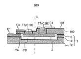
- FIG. 3 is a sectional view taken along the line A-A ′ of FIG. 2. It is a figure explaining the principle of operation of acceleration sensor S1.
- FIG. 1 It is a top view which shows the weight 2 with which acceleration detection element S1E is provided, and its periphery structure.
- FIG. 3 is a sectional view taken along the line A-A ′
- FIG. 8 is a cross-sectional view taken along line A-A ′ of FIG. 7. It is a figure explaining the structure of the acceleration sensor which concerns on Embodiment 3.
- FIG. It is a figure which shows the structural example which replaced with the level
- the constituent elements are not necessarily indispensable unless otherwise specified or apparently indispensable in principle.
- FIG. 1 is a schematic diagram showing an overall configuration of an acceleration sensor S1 according to Embodiment 1 of the present invention.
- the acceleration sensor S1 includes an acceleration detection element S1E, a signal processing IC (Integrated Circuit) 50, a lead frame 150, and a conductive wire 152.
- the conductive wire 152 electrically connects the acceleration detection element S1E, the signal processing IC 50, and the lead frame 150.
- the signal processing IC 50 and the acceleration detection element S1E are fixed on the lead frame 150 and the signal processing IC 50 through an adhesive 151, respectively.
- Acceleration sensor S1 is completed by press-molding thermosetting resin 153 and covering each part.
- the acceleration sensor S1 is incorporated in a higher system, and provides the detected physical quantity information to the higher system.
- FIG. 2 is a plan view showing the weight 2 provided in the acceleration detecting element S1E and its peripheral configuration.
- a plan view of the device layer 1c in a state where the cap layer 100 described later with reference to FIG. 3 is peeled off is shown.
- the acceleration detecting element S1E includes a weight 2 formed by processing by a method described later.
- the weight 2 is suspended by the fixed part 6 via the torsion beam 5, and is thereby configured to rotate around the y direction (second direction).
- the fixing portion 6 is fixed to the support substrate 1a via an intermediate insulating layer 1b described later. Accordingly, the weight 2 rotates around the second direction in proportion to the acceleration applied in the third direction (z direction), that is, is displaced in the third direction.
- the pad E1 will be described later.
- the acceleration detection element S1E includes, for example, an SOI (Silicon On Insulator) substrate 1 in order to form mechanical components such as the weight 2 and the fixed portion 6.
- the SOI substrate 1 has a configuration in which an intermediate insulating layer 1b is formed on a support substrate 1a, and a device layer 1c is formed on the intermediate insulating layer 1b.
- the support substrate 1a is made of, for example, silicon (Si).
- the intermediate insulating layer 1b is made of, for example, silicon oxide (SiO 2 ).
- the device layer 1c is made of, for example, conductive silicon.
- the total thickness of the support substrate 1a and the intermediate insulating layer 1b is, for example, several hundred ⁇ m.
- the thickness of the device layer 1c is, for example, several to several tens of ⁇ m.
- a semiconductor substrate other than the SOI substrate can be used.
- conductive polysilicon using surface MEMS technology or plated metal such as nickel (Ni) may be used as the device layer 1c.
- the SOI substrate 1 can also be formed by processing the cavity CD on the support substrate 1a and then thermally oxidizing to form the intermediate insulating layer 1b and further bonding the device layer 1c.
- Each component of the acceleration detection element S1E is formed by processing the device layer 1c and the cap layer 100.
- a method of processing the device layer 1c and the cap layer 100 there are the following methods. First, a resist that reacts to light, an electron beam, or the like is applied onto the device layer 1c or the cap layer 100, and then the resist on the device layer 1c or the cap layer 100 is applied using photolithography or an electron beam drawing technique. Remove some. Next, the exposed device layer 1c or the cap layer 100 is removed by using dry etching using RIE (Reactive Ion Etching) or wet etching using an alkaline chemical such as TMAH or KOH. Thereafter, by removing the remaining resist, each component described later can be formed on the device layer 1c and the cap layer 100.
- RIE Reactive Ion Etching
- TMAH TMAH
- KOH alkaline chemical
- fixed side electrodes C1B and C2B are formed in order to measure the displacement of the weight 2.
- the weight 2 plays a role as a drive side electrode.
- the fixed electrodes C1B and C2B and the driving electrode form detection electrodes C1 and C2 described later with reference to FIG.
- the capacitances of the detection electrodes C1 and C2 are arranged so that when one side increases in conjunction with the movement of the weight 2, the other side decreases. Therefore, an output proportional to the applied acceleration can be obtained by using the differential detection method described in FIG. Detailed description of each element constituting the circuit will be described later.
- the cap layer 100 is provided with a step as shown around the rotation center B of the weight 2. Due to this step, the left side stiffness and the right side stiffness of the rotation center B are different from each other. The reason for this will be described later with reference to FIG.
- the cap layer 100 is a layer for protecting the weight 2, the torsion beam 5, and the detection electrodes C1 and C2 from external impact, mechanical contact, dust, and the like.
- the cap layer 100 has a trench formed by a dry etching technique or the like.
- An insulating film 101 such as a thermal oxide film is buried in the trench, and thereby the airtightness of the cavity CD surrounded by the cap layer 100 and the support substrate 1 is maintained.
- the through electrodes T3 and T4 shown in FIG. 3 are formed by dividing the cap layer 100 by the trench and the insulating film 101, and function as the fixed-side electrodes C1B and C2B.
- the insulating film 101 can be formed, for example, by thermal oxidation after forming a trench, or by using CVD (Chemical Vapor Deposition).
- the cap layer 100 in which the insulating film 101 and the through electrodes T3 and T4 are formed is bonded to the SOI substrate 1 on which the weight 2, the torsion beam 5 and the like are formed, so that the weight 2 is mechanically contacted from the outside. And can be protected from dust.
- a bonding method (a) an eutectic bonding method in which an alloy such as gold or tin is applied between the cap layer 100 and the device layer 1c and then cured by heat treatment, and (b) the cap layer 100 and the device layer 1c.
- silicon-silicon or silicon-silicon oxide films are directly bonded to each other by hydrogen bonding at room temperature and heating at a high temperature after fabrication.
- Pads E1, E3, E4, and the like are formed in order to electrically connect the weight 2, the fixed side electrodes C1B and C2B, and the signal processing IC 50 described later.
- the pads E3 and E4 are connected to the through electrodes T3 and T4, respectively.
- the signal processing IC 50 can input and output electrical signals between the weight 2 and the fixed side electrodes C1B and C2B via the pads E1, E3, and E4.
- FIG. 4 is a diagram for explaining the operating principle of the acceleration sensor S1.
- the weight 2 is formed such that the weights on both sides of the central axis in the first direction (x direction) are different from each other with the torsion beam 5 as the central axis. That is, when acceleration is applied in the third direction (z direction), the force (F1) received by the left weight 2 (m1) of the torsion beam 5 and the force (F2) received by the right weight 2 (m2) are: The values are different from each other.
- Equation 1 shows the moment M generated in the torsion beam 5 when the acceleration a is applied in the third direction.
- a CV (Capacitance to Voltage) conversion circuit 52 which will be described later, performs differential detection using two detection electrodes C1 and C2 whose capacitance changes in accordance with displacement generated in the third direction.
- the displacement in the direction (change in capacitance) is converted into an electric signal (voltage).
- the through electrodes T3 and T4 formed on a part of the cap layer 100 as the fixed electrodes C1B and C2B of the detection electrodes C1 and C2 form a capacitance with the weight 2, and the CV conversion circuit 52 Detects changes in capacitance.
- the torsion beam 5 (rotation center) at a position away from the center of gravity of the weight 2.
- the detection electrodes C ⁇ b> 1 and C ⁇ b> 2 are formed so as to have the same capacitance at the same interval in the first direction when viewed from the torsion beam 5 in order to ensure the linearity of the sensor output with respect to the applied acceleration. Therefore, the detection electrodes C1 and C2 are necessarily arranged at positions away from the center of the cavity CA formed by the support substrate 1a and the cap layer 100.
- the through electrodes T3 and T4 having the role as the fixed side electrodes C1B and C2B are equal in the first direction (x direction) when viewed from the torsion beam 5 (the rotation center of the weight 2). Arranged at a distance.
- the capacitance formed by the left side portion of the weight 2 around the beam 5 and the fixed side electrode C1B is arranged to be the same as the capacitance formed by the right side portion of the weight 2 and the fixed side electrode C2B. Has been.
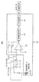
- FIG. 5 is a circuit diagram of the signal processing IC 50.
- the signal processing IC 50 applies the carrier wave 51 to the fixed side electrodes C1B and C2B via the pads E3 and E4.
- the weight 2 is connected to the input terminal of the CV conversion circuit 52 via the torsion beam 5, the fixing portion 6, and the pad E1. Thereby, a change in electrostatic capacitance between the weight 2 and the fixed side electrodes C1B and C2B can be detected.
- the synchronous detection circuit 53 restores the amplitude and frequency following the movement of the weight 2 by processing the output signal from the CV conversion circuit 52 using the frequency of the carrier wave 51.
- the AD converter 54 converts the result into a digital signal. Thereby, a signal Vo proportional to the acceleration applied to the weight 2 is output.
- the acceleration sensor S1 employs a package in which a thermosetting resin 153 is pressure-molded for cost reduction. Therefore, the acceleration detection element S1E receives a pressure generated when the thermosetting resin 153 is pressure-molded. Therefore, zero point drift may occur when the acceleration sensor S1 is shipped. Furthermore, the internal stress generated in the thermosetting resin 153 during the formation of the package fluctuates due to relaxation over time due to changes in environmental temperature and humidity. Therefore, even after the acceleration sensor S1 is shipped, zero point drift can occur.
- a step is provided in the cap layer 100 so that the rigidity of the portion corresponding to the fixed side electrode C1B and the rigidity of the portion corresponding to the fixed side electrode C2B are different from each other. Yes.
- the specific configuration will be described below.
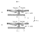
- FIG. 6 is a diagram showing a result of analyzing the deformation state of the cap layer 100 and the fixed side electrodes C1B and C2B by the finite element method when a pressure of several Mpa is applied to the cap layer 100.
- FIG. FIG. 6A shows an analysis result when the cap layer 100 has no step t.
- FIG. 6B shows an analysis result when a step t is provided in the cap layer 100.
- the inflection point of deformation of the cap layer 100 is located at the center of the cavity CA.
- the displacement amounts of the fixed side electrodes C1B and C2B arranged symmetrically about the rotation center B in the third direction (z direction) are different from each other.
- the capacitance changes ⁇ C1 and ⁇ C2 of the detection electrodes C1 and C2 are also different from each other, and a non-zero value that is originally expected as the sensor output (initial zero point) is output.
- the inflection point of the deformation of the cap layer 100 is located immediately above the rotation center B of the weight 2.
- the fixed side electrode C1B , C2B has the same displacement amount in the third direction (z direction). Accordingly, the capacitance changes ⁇ C1 and ⁇ C2 of the detection electrodes C1 and C2 also have the same value, and these fluctuations are offset by the differential detection, so that the sensor output becomes a value as originally expected.
- thermosetting resin 153 When the internal stress is relaxed over time and the capacitance changes ⁇ C1 and ⁇ C2 change, (b) the capacitance change ⁇ C is caused by the curable resin 153 expanding by sucking moisture from the environment.
- C1 and ⁇ C2 fluctuate, (c) capacitance changes ⁇ C1 and ⁇ C2 due to mounting stress and strain generated when the lead frame 150 is constrained on a specific substrate by soldering or the like, and variations with time. Even when the value fluctuates, the output drift (fluctuation) of the acceleration sensor S1 can be suppressed.
- the portion corresponding to the fixed side electrode C1B and the portion corresponding to the fixed side electrode C2B of the cap layer 100 have different thicknesses. Specifically, the portion corresponding to the fixed side electrode C1B arranged on the light side with the rotation center B of the weight 2 as the center is formed thinner than the portion corresponding to the fixed side electrode C2B arranged on the heavy side. Has been. Thereby, the displacement amount of each detection electrode C1 and C2 which generate
- thermosetting resin 153 In the first embodiment, an example in which packaging is performed by press-molding the thermosetting resin 153 is shown.
- the present invention is not limited to the packaging method in which the thermosetting resin 153 is pressure-molded, and even in a package in which the acceleration detection element S1E is put in a container that is shaped in advance, such as a ceramic package, and the lid is covered. Needless to say, similar effects can be obtained.
- the acceleration detection element S1E is a composite of thin layers made of different materials such as the support substrate 1a, the intermediate insulating layer 1b, the device layer 1c, the cap layer 100, the lead frame 150, the signal processing IC 50, and the adhesive 151.
- the material is configured as a body and the linear expansion coefficients of the respective constituent materials are different, so that distortion occurs due to a change in environmental temperature.
- the inflection point is adjusted to be located at the rotation center B by reducing the thickness of the cap layer 100 on the left side of the rotation center B, that is, in the direction in which the cavity CA is small. Similarly, the same effect can be expected even if the cap layer 100 on the right side of the rotation center B is thickened. Further, although not shown, it is needless to say that the same effect can be obtained even if the step t is arranged not only in one but also in a slit shape. Further, the step can be configured in a multi-step manner.
- the cavity CA is formed so as to surround the simplest plate-shaped weight 2 and the gaps at equal intervals (minimum), processing and manufacturing processes are simple, and the area is used. It can be said that the efficiency is high. That is, it can be said that it is advantageous for miniaturization.
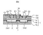
- FIG. 7 is a plan view showing main components of the acceleration sensor S2 according to the second embodiment of the present invention.
- FIG. 7 shows a state in which the cap layer 100 is peeled off as in FIG. Below, the part which overlaps with the content demonstrated about acceleration sensor S1 of Embodiment 1 is omitted, and the changed and added part is demonstrated intensively.
- the manufacturing method of the acceleration sensor S2 is the same as that of the acceleration sensor S1 in the first embodiment.
- the difference from the first embodiment is that the weight 2 is arranged so as to surround the fixed portion 6, that is, the fixed portion 6 is formed inside the weight 2, and the fixed portion 6 and the signal are connected via the through electrodes T 1 and T 2. That is, the processing IC 50 is electrically connected.
- the through electrodes T1 and T2 are configured to mechanically connect the device layer 1c and the cap layer 100, they serve as posts that suppress deformation of the cap layer 100 due to external pressure application. Also have.
- a fixed portion 6 is formed inside the weight 2
- a torsion beam 5 is formed so as to extend from the fixed portion 6 in the second direction
- a weight is formed at the tip of the torsion beam 5. 2 are connected.
- the fixing portion 6 is fixed to the supporting substrate 1a via the intermediate insulating layer 1b in the vicinity of the center portion of the cavity CA formed by the supporting substrate 1a and the cap layer 100 so as to surround the weight 2.
- FIG. 8 is a cross-sectional view taken along the line A-A ′ of FIG.
- the acceleration sensor S2 detects the displacement of the weight 2 so that the through electrodes T3 and T4 functioning as the fixed-side electrodes C1B and C2B are formed in the cap layer 100. It has a capacitance. Pads E3 and E4 are formed on the through electrodes T3 and T4, and are electrically connected to the signal processing IC 50.
- the through electrodes T1 and T2 penetrate the cap layer 100 from above the fixed portion 6 and reach the fixed portion 6.
- the through electrodes T1 and T2 are disposed along the rotation axis B.
- a pad E1 is connected to the through electrodes T1 and T2.
- the signal processing IC 50 inputs and outputs electrical signals through the pad E1 and the through electrodes T1 and T2. As a result, the electric signal propagates to the weight 2 through the fixed portion 6.
- only one through electrode is sufficient, but by providing a plurality of through electrodes, the connection between the cap layer 100 and the device layer 1c can be determined.
- a closed loop can be formed for inspection.
- the through electrodes T1 and T2 serve as electrodes that electrically connect the weight 2 and the signal processing IC 50 and also serve as posts that prevent the cap layer 100 from collapsing.
- the cap layer 100 In order to measure the displacement of the weight 2 in the third direction (z direction), a part of the cap layer 100 is formed as the through electrodes T3 and T4, which are used as the fixed electrodes C1B and C2B. Therefore, when the thermosetting resin 153 is pressure-molded, the capacitances of the detection electrodes C1 and C2 also change according to the deformation of the cap layer 100.
- the acceleration detecting element S2E uses a laminated structure of a plurality of different materials such as silicon as the support substrate 1a, silicon oxide as the intermediate insulating layer 1b, and metal materials such as aluminum as the pads E1, E3, and E4. It is made as. Therefore, it is easily conceivable that the capacitance of the detection electrodes C1 and C2 changes due to the deformation of the acceleration detection element S2E or the cap layer 100 due to a change in environmental temperature.
- Capacitance changes of the detection electrodes C1 and C2 are caused by equal capacitances in the first direction (x direction) with the detection electrodes C1 and C2 having the torsion beam 5 (rotation center: B line) as an axis of symmetry.
- a step t is formed in the cap layer 100, the inflection point of deformation of the cap layer 100 is aligned with the rotation center, and a positive carrier wave is applied to the detection electrode C1.
- a negative carrier wave is applied to the detection electrode C2, and the sum is input to the CV conversion circuit 52 to perform differential detection, so that it can be canceled theoretically.
- 0-point output of the sensor at the initial stage (0-point output that does not change at the product shipment stage: 0-point output is the sensor output when no acceleration is applied to the sensor and is expected to be 0)
- thermosetting resin 153 In the case of a package employing the thermosetting resin 153, an internal stress is generated inside the resin during pressure molding, and this internal stress is relieved with time. The amount of deformation of 100 also changes over time. Furthermore, the volume of the thermosetting resin 153 increases or decreases according to the environmental humidity. That is, the deformation amount of the cap layer 100 changes depending on the environmental humidity. The zero point drift depending on these environmental and temporal factors cannot be electrically corrected.
- the initial and temporal fluctuations of the detection electrodes C1 and C2 are suppressed, and even when there is a fluctuation, the fluctuation amount is made the same between C1 and C2, so that It needs to be able to offset.
- a plurality of through electrodes T1 and T2 are provided along the rotation axis (twisted beam 5) to serve as posts, thereby minimizing the deformation of the cap layer 100 and reducing the cap layer.
- a step t it is useful that the capacitance variations of the detection electrodes C1 and C2 are made the same and can be canceled by differential detection even if deformation occurs.
- the fixed portion 6 is arranged near the center of the cavity CA, and (configuration b) a plurality of posts (through electrodes T1, T2) are arranged on the fixed portion 6 along the rotation axis.
- the detection electrodes C1 and C2 are arranged at equal intervals and the same capacity in the first direction (x direction) with the torsion beam 5 (rotation axis: B line) as the axis of symmetry.
- the cap layer 100 has a step t and is configured such that the capacitance changes of the detection electrodes C1 and C2 are the same even when the cap layer 100 is deformed.
- a cap layer is formed by disposing the fixed portion 6 and the beam 5 near the center of the cavity CA (B line in FIG. 7) and disposing the through electrodes T1 and T2 along the rotation axis (B line) on the fixed portion 6. Even when a pressure is applied from the outside to 100, the amount of deformation is made as small as possible. Further, since the cap layer 100 has the step t, even if the cap layer 100 is deformed, the capacitance changes of the detection electrodes C1 and C2 are the same, so the influence of the deformation is offset by differential detection. can do.
- the cap layer 100 It can easily be considered to reduce the deformation amount of the cap layer 100 by increasing the thickness of the cap layer 100.
- a narrow trench is processed in the cap layer 100, and the insulating film 101 (the through electrodes T1, T2 in FIGS. , T3 and T4).
- the ratio of the width of the trench to the thickness of the cap layer 100 is 20 or less, so that mass production is possible. Therefore, increasing the thickness of the cap layer 100 has a limit from the viewpoint of mass productivity.
- the width of the trench is several ⁇ m, and the thickness of the cap layer 100 is 100 to 400 ⁇ m.
- Detecting electrodes C1 and C2 are arranged at equal intervals and the same capacity in the first direction (x direction) with the torsion beam 5 (B line) as the axis of symmetry. Further, the thickness of the cap layer 100 on the cavity CA2 side, which is short in the first direction from the rotation center (B line), is formed thinner than the thickness of the cap layer 100 on the opposite side of the cavity CA1. That is, adjustment is made so that the rigidity in the third direction of the fixed side electrodes C1B and C2B of the detection electrodes C1 and C2 is approximately the same. Therefore, even when the cap layer 100 is deformed by the application of pressure from the outside or a change in the surrounding environment, the capacitance fluctuations of the detection electrodes C1 and C2 are the same, and the influence can be offset by differential detection.
- the acceleration sensor S ⁇ b> 2 uses the through electrodes T ⁇ b> 1 and T ⁇ b> 2 installed to apply an electric signal to the weight 2 as a post supporting the cap layer 100, thereby 100 deformations can be reduced. Furthermore, by providing the step t in the cap layer 100, it is possible to cancel the fluctuations in the capacitance of the detection electrodes C1 and C2 due to external pressure and environmental fluctuations, and to improve the stability of the zero point output of the sensor.
- the capacitance variation amounts of the detection electrodes C1 and C2 are made the same.
- the essence of Embodiment 1 is that the inflection point of the cap layer 100 coincides with the rotation center (B line).
- the essence of the second embodiment is to make the through electrodes T3 and T4 have the same rigidity. That is, by adjusting the rigidity of the through-electrodes T3 and T4 according to the sizes of the cavities CA1 and CA2, the amount of deformation caused by external pressure application or environmental fluctuation can be made the same.
- FIG. 9 is a diagram illustrating the configuration of the acceleration sensor according to the third embodiment.
- FIG. 9C is a plan view of the acceleration sensor according to the third embodiment, and shows a state where the cap layer 100 is peeled off as in FIG.
- FIG. 9D is a cross-sectional view taken along the line D-D ′ of FIG.
- FIG. 9A is a plan view of the acceleration sensor S1 according to the first embodiment, and is shown together with FIG. 9C for comparison.
- FIG. 9B is a cross-sectional view taken along the line C-C ′ of FIG.
- a hole 10 is used instead of the step t.
- the hole 10 is formed so as not to penetrate the cap layer 100 along the third direction (z direction) from the insulating film 101 side toward the weight 2.
- Other configurations are the same as those in the first and second embodiments.
- the inflection point of the cap layer 100 can be variously adjusted by adjusting the arrangement, size, pitch, and depth of the holes 10. Specifically, by forming more holes 10 on the left side of the rotation axis B than on the right side, the rigidity of the cap layer 100 on the left side of the rotation axis B can be made weaker than that on the right side. Further, by using the hole 10, unlike the case where the step t is provided, the thickness of the cap layer 100 can be kept constant. Therefore, the insulating layer 101 and the pads E3 and E4 arranged on the cap layer 100 can be formed by a simpler manufacturing method.
- a cylindrical hole 10 that does not penetrate the cap layer 100 is provided in the cap layer 100.
- a hole having a shape such as a square or a band (groove) is provided in the cap layer 100.
- the hole is not limited to a circular hole.
- FIG. 10 is a diagram illustrating a configuration example in which the groove 11 is provided in the cap layer 100 in place of the step t in order to adjust the inflection point of the cap layer 100.
- FIG. 10A is a plan view of the cap layer 100
- FIG. 10B is a cross-sectional view taken along the line E-E 'of FIG.
- the groove 11 is formed on the bottom surface of the cap layer 100, that is, on the cavity CA side.
- the arrangement of the fixing portion 6 described in the second embodiment is assumed, but the groove 11 can be provided in the configuration described in the first embodiment.
- FIG. 11 is a diagram showing a result of analyzing the deformation state of the cap layer 100 by a finite element method.
- FIG. 11A shows an analysis result when there is no groove 11
- FIG. 11B shows an analysis result when the groove 11 is present.
- the displacement amounts of the through electrodes T3 and T4 in the third direction can be made substantially the same. Accordingly, since the capacitance changes ⁇ C1 and ⁇ C2 have the same value, the influence of deformation of the cap layer 100 can be offset by using differential detection.
- ⁇ Embodiment 3 Supplement about hole 10 and groove 11> All the depressions such as the hole 10 and the groove 11 for adjusting the inflection point and rigidity of the cap layer 100 are arranged so as not to straddle the insulating film 101 and the trench that separates the fixed-side electrodes C1B and C2B from the surrounding silicon. Has been.
- the first embodiment is performed in order to remove silicon of the cap layer 100 and silicon oxide constituting the insulating layer 101.
- a manufacturing step different from ⁇ 2 is required.
- SF6 is used as a reactive gas in order to remove silicon
- CHF3 is used as a reactive gas in order to remove a silicon oxide film, so that the manufacturing process becomes somewhat complicated.
- the depressions such as the holes 10 and the grooves 11 are formed so as not to cross the trench, only the silicon needs to be processed, so that the manufacturing process can be simplified.
- the depressions such as the holes 10 and the grooves 11 are formed in the cap layer 100 along the third direction from the outer side of the cap layer 100 (that is, the surface not facing the weight 2) toward the weight 2.
- the distance between the fixed side electrode C1B or C2B and the weight 2 is not affected by the presence of the depression. Therefore, in this case, as shown by the hole 10 in FIG. 9C, the position overlaps with the fixed side electrode C1B or C2B in the third direction (z direction) (FIG. 9C ) May be disposed in the inner part surrounded by a dotted line), or may be disposed in a position that does not overlap (an outer part not surrounded by the dotted line in FIG. 9C). Therefore, the inflection point and rigidity of the cap layer 100 can be adjusted extensively without affecting the capacitance of the detection electrodes C1 and C2.
- the cap layer 100 is formed along the third direction with the depressions such as the holes 10 and the grooves 11 from the inner side of the cap layer 100 (ie, the surface facing the weight 2) toward the opposite surface.
- the hole 10 or the groove 11 is located between the fixed side electrode C1B or C2B and the weight 2, so that the detection electrodes C1 and C2 and the weight depend on the positions of these depressions.
- the capacitance formed by 2 is affected. Therefore, in this case, it is desirable to arrange the depression at a position that does not overlap with the fixed side electrode C1B or C2B in the third direction (z direction).
- the degree of freedom for adjusting the inflection point and the rigidity of the cap layer 100 is reduced as compared with the case where the depression is formed from the outside to the inside of the cap layer 100.
- the pads E1, E3, E4, etc. on the depressions since it is not necessary to form the pads E1, E3, E4, etc. on the depressions, the formation and arrangement of the pads E1, E3, E4 and the routing of the wiring are facilitated.
- the present invention is not limited to the embodiments described above, and includes various modifications.
- the above embodiment has been described in detail for easy understanding of the present invention, and is not necessarily limited to the one having all the configurations described.
- the step t, the hole 10 and the groove 11 are exemplified as means for adjusting the rigidity of the cap layer 100.
- the cap is formed on both sides of the rotation axis B. If the mass per unit area in the XY plane of the layer 100 can be configured to be different from each other, it is considered that the same effect can be exhibited.
- the step t, the hole 10, and the groove 11 are used to change the inflection point and rigidity of the cap layer 100, and the third direction of the fixed side electrodes T3 (C1B) and T4 (C2B). It was shown that the amount of displacement in can be adjusted. However, it is needless to say that these methods are not limited to those independent from each other, and can be variously modified without departing from the gist thereof.
- the recesses can be formed on the front or back of the cap layer 100 by combining the holes 10 and the grooves 11.
- the step t may be combined as necessary.
- the packaging technology using the thermosetting resin 153 has been described for convenience of explanation.
- the acceleration detecting element is composed of a plurality of materials, the linear expansion coefficient is Deformation of the acceleration detection element due to the difference is easily assumed. Therefore, the concept of the present invention is also useful in various packaging technologies that involve deformation of the acceleration detecting element itself or distortion due to mounting, such as a ceramic package or a pre-molded package in which plastic is molded in advance and components are mounted therein. is there.
- the present invention can be widely used in the fields of attitude detection of automobiles, robots, etc., camera shake correction, navigation attitude / direction detection, game machine attitude detection sensors, and the like. In particular, it can be expected to exert its effect when used in a moving body or when there are heat sources such as engines, motors, electromagnets, and microcomputers in the vicinity.
- S1 to S2 Acceleration sensor 1a: Support substrate 1b: Intermediate insulating layer 1c: Device layer 2: Weight 5: Torsion beam 6: Fixing part C1 to C2: Detection electrode C1B: Detection electrode fixed side electrode C2B: Detection electrode fixing Side electrode CA: Cavity CA1: Cavity CA2: Cavity T1-T2: Through electrode (post) T3 to T4: Through electrode (detection electrode fixed side electrode) E1 to E4: Pad 101: Insulating film 50: Signal processing IC 51: Carrier 52: CV conversion circuit 53: Synchronous detection circuit 54: AD conversion unit 100: Cap layer 150: Lead frame 151: Adhesive 152: Wire 153: Thermosetting resin
Landscapes
- Physics & Mathematics (AREA)
- General Physics & Mathematics (AREA)
- Pressure Sensors (AREA)
Abstract
Description
、一方は他方の一部または全部の変形例、詳細、補足説明等の関係にある。
、その繰り返しの説明は可能な限り省略するようにしている。なお、図面をわかりやすくするために平面図であってもハッチングを付す場合がある。以下、本発明の実施形態を図面に基づいて説明する。
図1は、本発明の実施形態1に係る加速度センサS1の全体構成を示す模式図である。加速度センサS1は、加速度検出素子S1E、信号処理IC(Integrated Circuit)50、リードフレーム150、導電性ワイヤ152を備える。導電性ワイヤ152は、加速度検出素子S1E、信号処理IC50、リードフレーム150間を電気的に接続する。信号処理IC50と加速度検出素子S1Eは、接着剤151を介してそれぞれリードフレーム150と信号処理IC50上に固定される。
金をキャップ層100とデバイス層1cの間に塗布した後、熱処理することで硬化させる共晶接合法、(b)キャプ層100とデバイス層1cの表面をプラズマで活性化し、シリ
コン‐シリコンまたはシリコン‐シリコン酸化膜同士を直接接合する常温活性化接合法、(c)2つの表面を酸と純水の混合液で洗浄し、表面に水酸基を作った後、常温で水素結合させ、高温で加熱することにより、シリコン‐シリコンまたはシリコン‐シリコン酸化膜同士を直接接合する方法、などがある。
Θ=M/k 式2)
加速度センサS1は、低コスト化のため、熱硬化性樹脂153を加圧成形したパッケージを採用している。そのため、加速度検出素子S1Eは、熱硬化性樹脂153を加圧成形する際に発生する圧力を受けることになる。そのため加速度センサS1の出荷時において0点ドリフトが生じ得る。さらに、パッケージの形成時に熱硬化性樹脂153の内部に発生する内部応力は、環境温度や湿度の変化によって経時的に緩和するなどして変動する。そのため加速度センサS1を出荷した後においても0点ドリフトが生じ得る。
、C2Bの第3方向(z方向)における変位量は、互いに同じ値となる。したがって、検出電極C1、C2の容量変化ΔC1、ΔC2も同じ値となり、これらの変動分は差動検出によって相殺されるため、センサ出力は本来の期待通りの値となる。
樹脂153の内部の応力が経時的に緩和されて静電容量変化ΔC1、ΔC2が変動する場合、(b)硬化性樹脂153が環境から水分を吸って膨張することにより静電容量変化Δ
C1、ΔC2が変動する場合、(c)リードフレーム150を特定の基板上に半田付けな
どで拘束する際に発生する実装応力やひずみ、またこれらの経時的な変動によって静電容量変化ΔC1、ΔC2が変動する場合、などにおいても、加速度センサS1の出力ドリフト(変動)を抑制することができる。
以上のように、本実施形態1に係る加速度センサS1において、キャップ層100の固定側電極C1Bに対応する部分と固定側電極C2Bに対応する部分は互いに異なる厚さを有する。具体的には、錘2の回転中心Bを中心として軽い側に配置されている固定側電極C1Bに対応する部分は、重い側に配置されている固定側電極C2Bに対応する部分よりも薄く形成されている。これにより、熱硬化性樹脂153を加圧成形する際に発生する各検出電極C1、C2の変位量を同じくすることができる。この変位量は差動検出によって相殺できるため、加速度センサS1の初期0点および、環境温度、湿度、熱硬化性樹脂153の内部応力の緩和などに依存する経時的な0点の変動を抑制することができる。
図7は、本発明の実施形態2に係る加速度センサS2の主要な構成要素を示す平面図である。図7は図2と同様に、キャップ層100を剥がした状態を示している。以下では実施形態1の加速度センサS1について説明した内容と重複する部分は省いて、変更・追加された部分を重点的に説明する。
置し、(構成b)回転軸に沿って複数個のポスト(貫通電極T1、T2)を固定部6上に
配置し、(構成c)検出電極C1、C2は、ねじれ梁5(回転軸:Bライン)を対称軸と
して第1方向(x方向)に等間隔および同じ容量になるように配置し、(構成d)キャッ
プ層100は段差tを有し、キャップ層100が変形した場合でも、検出電極C1、C2の容量変化が同じになるように構成している。これら(構成a)~(構成d)の効果について以下に説明する。
以上のように、本実施形態2に係る加速度センサS2は、錘2に電気信号を印加するために設置した貫通電極T1、T2を、キャップ層100を支えるポストとしても活用することにより、キャップ層100の変形を低減することができる。さらに、キャップ層100に段差tを設けることにより、外部からの圧力や環境変動による検出電極C1、C2の容量の変動を相殺し、センサの0点出力の安定性を向上させることができる。
形態1~2と同様の効果を発揮することができる。具体例については以下の実施形態3で説明する。
本発明の実施形態3では、キャップ層100の変曲点および固定側電極C1B、C2Bの剛性を調整する方法として、実施形態1~2で説明した構成とは異なる手法について説明する。
。その結果は加速度センサの出力として現れ、加速度が印加されていない状態でも何らかの信号が出力されることになり、期待する0点の値を得ることができない。
キャップ層100の変曲点および剛性を調整するための孔10や溝11などの窪みは全て、固定側電極C1B、C2Bを周辺のシリコンから分離するトレンチと絶縁膜101を跨らないように配置されている。
)の点線によって囲まれた内側部分)に窪みを配置してもよいし、重ならない位置(図9(c)の点線によって囲まれていない外側部分)に配置してもよい。そのため、検出電極C1、C2の容量に影響を与えることなく、キャップ層100の変曲点および剛性を広範に調整することができる。
本発明は上記した実施形態に限定されるものではなく、様々な変形例が含まれる。上記実施形態は本発明を分かりやすく説明するために詳細に説明したものであり、必ずしも説明した全ての構成を備えるものに限定されるものではない。例えば、上記実施形態においてはキャップ層100の剛性を調整する手段として、段差t、孔10、溝11を例示したが、これら以外の構造を用いる場合であっても、回転軸Bの両側においてキャップ層100のXY面内における単位面積当たりの質量を互いに異なるように構成することができれば、同様の効果を発揮することができると考えられる。
における変位量を調整することができることを示した。しかし、これらの方法は互いに独立したものに限定されるものではなく、その要旨を逸脱しない範囲で種々変更可能であることはいうまでもない。例えば、孔10と溝11を組み合わせてキャップ層100の表または裏にこれら窪みを形成することもできる。さらに、必要に応じて段差tを組み合わせてもよい。
1a:支持基板
1b:中間絶縁層
1c:デバイス層
2:錘
5:ねじれ梁
6:固定部
C1~C2:検出電極
C1B:検出電極の固定側電極
C2B:検出電極の固定側電極
CA:キャビティ
CA1:キャビティ
CA2:キャビティ
T1~T2:貫通電極(ポスト)
T3~T4:貫通電極(検出電極の固定側電極)
E1~E4:パッド
101:絶縁膜
50:信号処理IC
51:搬送波
52:CV変換回路
53:同期検波回路
54:AD変換部
100:キャップ層
150:リードフレーム
151:接着剤
152:ワイヤ
153:熱硬化性樹脂
Claims (12)
- 加速度を検出する加速度センサであって、
互いに直交する第1および第2方向によって形成される面内に配置された支持基板、
空隙部分を有し前記支持基板上に配置された固定部、
前記空隙部分を覆うキャップ層、
前記支持基板と前記キャップ層が前記空隙部分を囲むことによって形成されたキャビティ内に配置された錘、
前記固定部と前記錘との間を架橋する梁部、
前記キャップ層の一部として形成されるとともに前記梁部を挟んで配置され、それぞれ前記錘との間で静電容量を形成する第1および第2検出電極、
を備え、
前記錘は、前記第1および第2方向と直交する第3方向における加速度が印加されると前記梁部を回転軸として回転するように構成されるとともに、前記回転軸の両側の重さが互いに異なるように構成されており、
前記キャップ層は、前記第1および第2方向によって形成される面内における単位面積当たりの質量が、前記梁部を挟んだ両側において互いに異なるように形成されており、
前記回転軸を中心として前記錘の重さが軽い側における前記キャップ層の前記単位面積当たりの質量は、前記錘の重さが重い側における前記キャップ層の前記単位面積当たりの質量よりも軽い
ことを特徴とする加速度センサ。 - 前記キャップ層は、前記キャップ層を貫通することにより前記キャップ層を複数部分に分割して互いに電気的に分離するトレンチを有し、
前記キャップ層はさらに、前記キャップ層を貫通せず、かつ前記トレンチを跨らないように形成された窪みを有する
ことを特徴とする請求項1記載の加速度センサ。 - 前記キャップ層は、前記梁部を挟んだ両側において前記窪みを互いに異なる個数形成することにより、前記単位面積当たりの質量が前記梁部を挟んだ両側において互いに異なるように形成されている
ことを特徴とする請求項2記載の加速度センサ。 - 前記第1および第2検出電極は、前記キャップ層を前記トレンチによって分割することにより形成されており、
前記窪みは、前記キャップ層の前記錘と対向していない側の面から前記錘に向かって前記第3方向に沿って形成されている
ことを特徴とする請求項3記載の加速度センサ。 - 前記第1および第2電極は、前記キャップ層を前記トレンチによって分割することにより形成されており、
前記窪みは、前記キャップ層の前記錘と対向している側の面から前記錘に向かって前記第3方向に沿って形成されるとともに、前記第3方向において前記第1および第2検出電極と重ならない位置に配置されている
ことを特徴とする請求項3記載の加速度センサ。 - 前記加速度センサはさらに、前記第1および第2検出電極と前記錘との間で形成される静電容量を差動検出することにより前記加速度を検出する回路を備える
ことを特徴とする請求項1記載の加速度センサ。 - 前記錘は前記第1および第2方向によって形成される面内において前記固定部を囲むように形成され、前記固定部は前記回転軸上に配置されており、
前記加速度センサはさらに、前記キャップ層を貫通して前記固定部と接触する貫通電極を備える
ことを特徴とする請求項1記載の加速度センサ。 - 前記加速度センサはさらに、前記第1および第2検出電極と前記錘との間で形成される静電容量を検出するために必要な電気信号、または前記錘を駆動するために必要な電気信号を、前記貫通電極を介して前記錘との間で入出力する回路を備える
ことを特徴とする請求項7記載の加速度センサ。 - 前記支持基板、前記錘、および前記キャップ層は、シリコンを用いて形成されている
ことを特徴とする請求項1記載の加速度センサ。 - 前記支持基板、前記錘、および前記キャップ層は、加速度を検出する加速度検出素子として構成されており、
前記加速度センサはさらに、加圧成形された熱硬化性樹脂により形成されたパッケージを備え、
前記パッケージは、前記加速度検出素子をパッケージングする
ことを特徴とする請求項1記載の加速度センサ。 - 前記加速度センサはさらに、前記加速度検出素子との間で電気信号を送受信する回路を備え、
前記回路はリードフレーム上に配置されており、
前記加速度検出素子は前記回路上に配置されており、
前記回路と前記加速度検出素子は、導電性ワイヤによって接続されている
ことを特徴とする請求項10記載の加速度センサ。 - 前記キャップ層は、前記第3方向における厚さが異なる部分を有することにより、前記単位面積当たりの質量が前記梁部を挟んだ両側において互いに異なるように形成されている
ことを特徴とする請求項1記載の加速度センサ。
Priority Applications (3)
| Application Number | Priority Date | Filing Date | Title |
|---|---|---|---|
| US15/129,963 US9995762B2 (en) | 2014-04-03 | 2015-03-25 | Acceleration sensor |
| JP2016511572A JP6209270B2 (ja) | 2014-04-03 | 2015-03-25 | 加速度センサ |
| EP15772477.4A EP3128333B1 (en) | 2014-04-03 | 2015-03-25 | Acceleration sensor |
Applications Claiming Priority (2)
| Application Number | Priority Date | Filing Date | Title |
|---|---|---|---|
| JP2014077078 | 2014-04-03 | ||
| JP2014-077078 | 2014-04-03 |
Publications (1)
| Publication Number | Publication Date |
|---|---|
| WO2015151946A1 true WO2015151946A1 (ja) | 2015-10-08 |
Family
ID=54240273
Family Applications (1)
| Application Number | Title | Priority Date | Filing Date |
|---|---|---|---|
| PCT/JP2015/059015 WO2015151946A1 (ja) | 2014-04-03 | 2015-03-25 | 加速度センサ |
Country Status (4)
| Country | Link |
|---|---|
| US (1) | US9995762B2 (ja) |
| EP (1) | EP3128333B1 (ja) |
| JP (1) | JP6209270B2 (ja) |
| WO (1) | WO2015151946A1 (ja) |
Families Citing this family (6)
| Publication number | Priority date | Publication date | Assignee | Title |
|---|---|---|---|---|
| JP2019060675A (ja) * | 2017-09-26 | 2019-04-18 | セイコーエプソン株式会社 | 物理量センサー、物理量センサー装置、電子機器、および移動体 |
| CN110501522B (zh) * | 2019-09-16 | 2022-10-11 | 上海矽睿科技股份有限公司 | 一种微机电系统的电容式加速度计 |
| US11981560B2 (en) | 2020-06-09 | 2024-05-14 | Analog Devices, Inc. | Stress-isolated MEMS device comprising substrate having cavity and method of manufacture |
| CN111981985A (zh) * | 2020-08-31 | 2020-11-24 | 华中科技大学 | 一种工业机器人末端三维位置测量仪器与方法 |
| CN114280331B (zh) * | 2021-12-16 | 2024-05-17 | 绍兴圆方半导体有限公司 | 一种z轴加速度计 |
| CN115420907B (zh) * | 2022-11-02 | 2023-03-21 | 杭州麦新敏微科技有限责任公司 | 一种mems加速度计及其形成方法 |
Citations (5)
| Publication number | Priority date | Publication date | Assignee | Title |
|---|---|---|---|---|
| JPH09189716A (ja) * | 1995-11-07 | 1997-07-22 | Temic Telefunken Microelectron Gmbh | 超小型機械的加速度センサ |
| JP2000019198A (ja) * | 1998-06-29 | 2000-01-21 | Zexel Corp | 加速度センサ |
| JP2008544243A (ja) * | 2005-06-17 | 2008-12-04 | ヴェーテーイー テクノロジーズ オサケユキチュア | 容量性加速度センサーを製造する方法、および、容量性加速度センサー |
| JP2009002834A (ja) * | 2007-06-22 | 2009-01-08 | Hitachi Ltd | 角速度検出装置 |
| JP2013040856A (ja) * | 2011-08-17 | 2013-02-28 | Seiko Epson Corp | 物理量センサー及び電子機器 |
Family Cites Families (3)
| Publication number | Priority date | Publication date | Assignee | Title |
|---|---|---|---|---|
| EP2126155B1 (en) * | 2006-12-15 | 2019-03-13 | BAE Systems PLC | Improvements relating to thin film getter devices |
| DE102011011160B4 (de) * | 2011-01-05 | 2024-01-11 | Robert Bosch Gmbh | Mikromechanisches Bauteil und Herstellungsverfahren für ein mikromechanisches Bauteil |
| TWI530449B (zh) * | 2014-01-27 | 2016-04-21 | 立錡科技股份有限公司 | 複合微機電系統晶片及其製作方法 |
-
2015
- 2015-03-25 US US15/129,963 patent/US9995762B2/en active Active
- 2015-03-25 WO PCT/JP2015/059015 patent/WO2015151946A1/ja active Application Filing
- 2015-03-25 JP JP2016511572A patent/JP6209270B2/ja not_active Expired - Fee Related
- 2015-03-25 EP EP15772477.4A patent/EP3128333B1/en not_active Not-in-force
Patent Citations (5)
| Publication number | Priority date | Publication date | Assignee | Title |
|---|---|---|---|---|
| JPH09189716A (ja) * | 1995-11-07 | 1997-07-22 | Temic Telefunken Microelectron Gmbh | 超小型機械的加速度センサ |
| JP2000019198A (ja) * | 1998-06-29 | 2000-01-21 | Zexel Corp | 加速度センサ |
| JP2008544243A (ja) * | 2005-06-17 | 2008-12-04 | ヴェーテーイー テクノロジーズ オサケユキチュア | 容量性加速度センサーを製造する方法、および、容量性加速度センサー |
| JP2009002834A (ja) * | 2007-06-22 | 2009-01-08 | Hitachi Ltd | 角速度検出装置 |
| JP2013040856A (ja) * | 2011-08-17 | 2013-02-28 | Seiko Epson Corp | 物理量センサー及び電子機器 |
Also Published As
| Publication number | Publication date |
|---|---|
| EP3128333A1 (en) | 2017-02-08 |
| JP6209270B2 (ja) | 2017-10-04 |
| JPWO2015151946A1 (ja) | 2017-04-13 |
| US9995762B2 (en) | 2018-06-12 |
| EP3128333B1 (en) | 2018-06-27 |
| US20170138981A1 (en) | 2017-05-18 |
| EP3128333A4 (en) | 2017-12-27 |
Similar Documents
| Publication | Publication Date | Title |
|---|---|---|
| JP6209270B2 (ja) | 加速度センサ | |
| JP6580804B2 (ja) | Mems圧力センサとmems慣性センサの集積構造 | |
| JP5092462B2 (ja) | 力学量センサ | |
| JP5898283B2 (ja) | 微小電気機械システム | |
| JP6002481B2 (ja) | 慣性センサ | |
| US8759927B2 (en) | Hybrid intergrated component | |
| JP2010276508A (ja) | 加速度センサー素子およびこれを有する加速度センサー | |
| JP6285541B2 (ja) | 加速度検出装置 | |
| WO2015115365A1 (ja) | センサおよびその製造方法 | |
| JP6343102B2 (ja) | 慣性力センサ | |
| US11119117B2 (en) | Sensor | |
| JP2010085143A (ja) | 加速度センサー | |
| WO2015163300A1 (ja) | 加速度センサ | |
| JP5843302B1 (ja) | 複合センサデバイスの製造方法 | |
| KR20150142015A (ko) | 미소 전자 기계 디바이스 및 제조 방법 | |
| WO2016121453A1 (ja) | 半導体センサ装置 | |
| JP6555238B2 (ja) | 力学量センサおよびその製造方法 | |
| JP5821158B1 (ja) | 複合センサデバイス | |
| JP5299353B2 (ja) | 半導体装置 | |
| WO2014208043A1 (ja) | 物理量センサ | |
| JP2008244174A (ja) | センサ素子の製造方法 | |
| WO2018030045A1 (ja) | 力学量センサおよびその製造方法 | |
| JPWO2008149821A1 (ja) | センサ装置 | |
| JP2008185374A (ja) | センサ装置の製造方法 |
Legal Events
| Date | Code | Title | Description |
|---|---|---|---|
| 121 | Ep: the epo has been informed by wipo that ep was designated in this application |
Ref document number: 15772477 Country of ref document: EP Kind code of ref document: A1 |
|
| ENP | Entry into the national phase |
Ref document number: 2016511572 Country of ref document: JP Kind code of ref document: A |
|
| WWE | Wipo information: entry into national phase |
Ref document number: 15129963 Country of ref document: US |
|
| REEP | Request for entry into the european phase |
Ref document number: 2015772477 Country of ref document: EP |
|
| WWE | Wipo information: entry into national phase |
Ref document number: 2015772477 Country of ref document: EP |
|
| NENP | Non-entry into the national phase |
Ref country code: DE |