WO2015151426A1 - 半導体装置、積層型半導体装置、封止後積層型半導体装置、及びこれらの製造方法 - Google Patents
半導体装置、積層型半導体装置、封止後積層型半導体装置、及びこれらの製造方法 Download PDFInfo
- Publication number
- WO2015151426A1 WO2015151426A1 PCT/JP2015/001433 JP2015001433W WO2015151426A1 WO 2015151426 A1 WO2015151426 A1 WO 2015151426A1 JP 2015001433 W JP2015001433 W JP 2015001433W WO 2015151426 A1 WO2015151426 A1 WO 2015151426A1
- Authority
- WO
- WIPO (PCT)
- Prior art keywords
- insulating layer
- semiconductor device
- electrode
- semiconductor element
- forming
- Prior art date
- Legal status (The legal status is an assumption and is not a legal conclusion. Google has not performed a legal analysis and makes no representation as to the accuracy of the status listed.)
- Ceased
Links
Images


Classifications
-
- H—ELECTRICITY
- H01—ELECTRIC ELEMENTS
- H01L—SEMICONDUCTOR DEVICES NOT COVERED BY CLASS H10
- H01L23/00—Details of semiconductor or other solid state devices
- H01L23/562—Protection against mechanical damage
-
- C—CHEMISTRY; METALLURGY
- C08—ORGANIC MACROMOLECULAR COMPOUNDS; THEIR PREPARATION OR CHEMICAL WORKING-UP; COMPOSITIONS BASED THEREON
- C08L—COMPOSITIONS OF MACROMOLECULAR COMPOUNDS
- C08L83/00—Compositions of macromolecular compounds obtained by reactions forming in the main chain of the macromolecule a linkage containing silicon with or without sulfur, nitrogen, oxygen or carbon only; Compositions of derivatives of such polymers
- C08L83/14—Compositions of macromolecular compounds obtained by reactions forming in the main chain of the macromolecule a linkage containing silicon with or without sulfur, nitrogen, oxygen or carbon only; Compositions of derivatives of such polymers in which at least two but not all the silicon atoms are connected by linkages other than oxygen atoms
-
- C—CHEMISTRY; METALLURGY
- C09—DYES; PAINTS; POLISHES; NATURAL RESINS; ADHESIVES; COMPOSITIONS NOT OTHERWISE PROVIDED FOR; APPLICATIONS OF MATERIALS NOT OTHERWISE PROVIDED FOR
- C09D—COATING COMPOSITIONS, e.g. PAINTS, VARNISHES OR LACQUERS; FILLING PASTES; CHEMICAL PAINT OR INK REMOVERS; INKS; CORRECTING FLUIDS; WOODSTAINS; PASTES OR SOLIDS FOR COLOURING OR PRINTING; USE OF MATERIALS THEREFOR
- C09D163/00—Coating compositions based on epoxy resins; Coating compositions based on derivatives of epoxy resins
-
- C—CHEMISTRY; METALLURGY
- C09—DYES; PAINTS; POLISHES; NATURAL RESINS; ADHESIVES; COMPOSITIONS NOT OTHERWISE PROVIDED FOR; APPLICATIONS OF MATERIALS NOT OTHERWISE PROVIDED FOR
- C09D—COATING COMPOSITIONS, e.g. PAINTS, VARNISHES OR LACQUERS; FILLING PASTES; CHEMICAL PAINT OR INK REMOVERS; INKS; CORRECTING FLUIDS; WOODSTAINS; PASTES OR SOLIDS FOR COLOURING OR PRINTING; USE OF MATERIALS THEREFOR
- C09D183/00—Coating compositions based on macromolecular compounds obtained by reactions forming in the main chain of the macromolecule a linkage containing silicon, with or without sulfur, nitrogen, oxygen, or carbon only; Coating compositions based on derivatives of such polymers
- C09D183/14—Coating compositions based on macromolecular compounds obtained by reactions forming in the main chain of the macromolecule a linkage containing silicon, with or without sulfur, nitrogen, oxygen, or carbon only; Coating compositions based on derivatives of such polymers in which at least two but not all the silicon atoms are connected by linkages other than oxygen atoms
-
- C—CHEMISTRY; METALLURGY
- C23—COATING METALLIC MATERIAL; COATING MATERIAL WITH METALLIC MATERIAL; CHEMICAL SURFACE TREATMENT; DIFFUSION TREATMENT OF METALLIC MATERIAL; COATING BY VACUUM EVAPORATION, BY SPUTTERING, BY ION IMPLANTATION OR BY CHEMICAL VAPOUR DEPOSITION, IN GENERAL; INHIBITING CORROSION OF METALLIC MATERIAL OR INCRUSTATION IN GENERAL
- C23C—COATING METALLIC MATERIAL; COATING MATERIAL WITH METALLIC MATERIAL; SURFACE TREATMENT OF METALLIC MATERIAL BY DIFFUSION INTO THE SURFACE, BY CHEMICAL CONVERSION OR SUBSTITUTION; COATING BY VACUUM EVAPORATION, BY SPUTTERING, BY ION IMPLANTATION OR BY CHEMICAL VAPOUR DEPOSITION, IN GENERAL
- C23C14/00—Coating by vacuum evaporation, by sputtering or by ion implantation of the coating forming material
- C23C14/04—Coating on selected surface areas, e.g. using masks
- C23C14/042—Coating on selected surface areas, e.g. using masks using masks
-
- C—CHEMISTRY; METALLURGY
- C23—COATING METALLIC MATERIAL; COATING MATERIAL WITH METALLIC MATERIAL; CHEMICAL SURFACE TREATMENT; DIFFUSION TREATMENT OF METALLIC MATERIAL; COATING BY VACUUM EVAPORATION, BY SPUTTERING, BY ION IMPLANTATION OR BY CHEMICAL VAPOUR DEPOSITION, IN GENERAL; INHIBITING CORROSION OF METALLIC MATERIAL OR INCRUSTATION IN GENERAL
- C23C—COATING METALLIC MATERIAL; COATING MATERIAL WITH METALLIC MATERIAL; SURFACE TREATMENT OF METALLIC MATERIAL BY DIFFUSION INTO THE SURFACE, BY CHEMICAL CONVERSION OR SUBSTITUTION; COATING BY VACUUM EVAPORATION, BY SPUTTERING, BY ION IMPLANTATION OR BY CHEMICAL VAPOUR DEPOSITION, IN GENERAL
- C23C14/00—Coating by vacuum evaporation, by sputtering or by ion implantation of the coating forming material
- C23C14/22—Coating by vacuum evaporation, by sputtering or by ion implantation of the coating forming material characterised by the process of coating
- C23C14/34—Sputtering
-
- C—CHEMISTRY; METALLURGY
- C25—ELECTROLYTIC OR ELECTROPHORETIC PROCESSES; APPARATUS THEREFOR
- C25D—PROCESSES FOR THE ELECTROLYTIC OR ELECTROPHORETIC PRODUCTION OF COATINGS; ELECTROFORMING; APPARATUS THEREFOR
- C25D5/00—Electroplating characterised by the process; Pretreatment or after-treatment of workpieces
- C25D5/02—Electroplating of selected surface areas
- C25D5/022—Electroplating of selected surface areas using masking means
-
- C—CHEMISTRY; METALLURGY
- C25—ELECTROLYTIC OR ELECTROPHORETIC PROCESSES; APPARATUS THEREFOR
- C25D—PROCESSES FOR THE ELECTROLYTIC OR ELECTROPHORETIC PRODUCTION OF COATINGS; ELECTROFORMING; APPARATUS THEREFOR
- C25D5/00—Electroplating characterised by the process; Pretreatment or after-treatment of workpieces
- C25D5/48—After-treatment of electroplated surfaces
- C25D5/50—After-treatment of electroplated surfaces by heat-treatment
- C25D5/505—After-treatment of electroplated surfaces by heat-treatment of electroplated tin coatings, e.g. by melting
-
- C—CHEMISTRY; METALLURGY
- C25—ELECTROLYTIC OR ELECTROPHORETIC PROCESSES; APPARATUS THEREFOR
- C25D—PROCESSES FOR THE ELECTROLYTIC OR ELECTROPHORETIC PRODUCTION OF COATINGS; ELECTROFORMING; APPARATUS THEREFOR
- C25D7/00—Electroplating characterised by the article coated
- C25D7/12—Semiconductors
- C25D7/123—Semiconductors first coated with a seed layer or a conductive layer
-
- G—PHYSICS
- G03—PHOTOGRAPHY; CINEMATOGRAPHY; ANALOGOUS TECHNIQUES USING WAVES OTHER THAN OPTICAL WAVES; ELECTROGRAPHY; HOLOGRAPHY
- G03F—PHOTOMECHANICAL PRODUCTION OF TEXTURED OR PATTERNED SURFACES, e.g. FOR PRINTING, FOR PROCESSING OF SEMICONDUCTOR DEVICES; MATERIALS THEREFOR; ORIGINALS THEREFOR; APPARATUS SPECIALLY ADAPTED THEREFOR
- G03F7/00—Photomechanical, e.g. photolithographic, production of textured or patterned surfaces, e.g. printing surfaces; Materials therefor, e.g. comprising photoresists; Apparatus specially adapted therefor
- G03F7/0035—Multiple processes, e.g. applying a further resist layer on an already in a previously step, processed pattern or textured surface
-
- G—PHYSICS
- G03—PHOTOGRAPHY; CINEMATOGRAPHY; ANALOGOUS TECHNIQUES USING WAVES OTHER THAN OPTICAL WAVES; ELECTROGRAPHY; HOLOGRAPHY
- G03F—PHOTOMECHANICAL PRODUCTION OF TEXTURED OR PATTERNED SURFACES, e.g. FOR PRINTING, FOR PROCESSING OF SEMICONDUCTOR DEVICES; MATERIALS THEREFOR; ORIGINALS THEREFOR; APPARATUS SPECIALLY ADAPTED THEREFOR
- G03F7/00—Photomechanical, e.g. photolithographic, production of textured or patterned surfaces, e.g. printing surfaces; Materials therefor, e.g. comprising photoresists; Apparatus specially adapted therefor
- G03F7/004—Photosensitive materials
- G03F7/075—Silicon-containing compounds
- G03F7/0757—Macromolecular compounds containing Si-O, Si-C or Si-N bonds
-
- H—ELECTRICITY
- H01—ELECTRIC ELEMENTS
- H01L—SEMICONDUCTOR DEVICES NOT COVERED BY CLASS H10
- H01L21/00—Processes or apparatus adapted for the manufacture or treatment of semiconductor or solid state devices or of parts thereof
- H01L21/02—Manufacture or treatment of semiconductor devices or of parts thereof
- H01L21/04—Manufacture or treatment of semiconductor devices or of parts thereof the devices having potential barriers, e.g. a PN junction, depletion layer or carrier concentration layer
- H01L21/48—Manufacture or treatment of parts, e.g. containers, prior to assembly of the devices, using processes not provided for in a single one of the groups H01L21/18 - H01L21/326 or H10D48/04 - H10D48/07
- H01L21/4814—Conductive parts
- H01L21/4846—Leads on or in insulating or insulated substrates, e.g. metallisation
- H01L21/4853—Connection or disconnection of other leads to or from a metallisation, e.g. pins, wires, bumps
-
- H—ELECTRICITY
- H01—ELECTRIC ELEMENTS
- H01L—SEMICONDUCTOR DEVICES NOT COVERED BY CLASS H10
- H01L21/00—Processes or apparatus adapted for the manufacture or treatment of semiconductor or solid state devices or of parts thereof
- H01L21/02—Manufacture or treatment of semiconductor devices or of parts thereof
- H01L21/04—Manufacture or treatment of semiconductor devices or of parts thereof the devices having potential barriers, e.g. a PN junction, depletion layer or carrier concentration layer
- H01L21/48—Manufacture or treatment of parts, e.g. containers, prior to assembly of the devices, using processes not provided for in a single one of the groups H01L21/18 - H01L21/326 or H10D48/04 - H10D48/07
- H01L21/4814—Conductive parts
- H01L21/4846—Leads on or in insulating or insulated substrates, e.g. metallisation
- H01L21/486—Via connections through the substrate with or without pins
-
- H—ELECTRICITY
- H01—ELECTRIC ELEMENTS
- H01L—SEMICONDUCTOR DEVICES NOT COVERED BY CLASS H10
- H01L21/00—Processes or apparatus adapted for the manufacture or treatment of semiconductor or solid state devices or of parts thereof
- H01L21/02—Manufacture or treatment of semiconductor devices or of parts thereof
- H01L21/04—Manufacture or treatment of semiconductor devices or of parts thereof the devices having potential barriers, e.g. a PN junction, depletion layer or carrier concentration layer
- H01L21/50—Assembly of semiconductor devices using processes or apparatus not provided for in a single one of the groups H01L21/18 - H01L21/326 or H10D48/04 - H10D48/07 e.g. sealing of a cap to a base of a container
- H01L21/56—Encapsulations, e.g. encapsulation layers, coatings
- H01L21/565—Moulds
-
- H—ELECTRICITY
- H01—ELECTRIC ELEMENTS
- H01L—SEMICONDUCTOR DEVICES NOT COVERED BY CLASS H10
- H01L23/00—Details of semiconductor or other solid state devices
- H01L23/12—Mountings, e.g. non-detachable insulating substrates
-
- H—ELECTRICITY
- H01—ELECTRIC ELEMENTS
- H01L—SEMICONDUCTOR DEVICES NOT COVERED BY CLASS H10
- H01L23/00—Details of semiconductor or other solid state devices
- H01L23/28—Encapsulations, e.g. encapsulating layers, coatings, e.g. for protection
- H01L23/31—Encapsulations, e.g. encapsulating layers, coatings, e.g. for protection characterised by the arrangement or shape
- H01L23/3107—Encapsulations, e.g. encapsulating layers, coatings, e.g. for protection characterised by the arrangement or shape the device being completely enclosed
- H01L23/3114—Encapsulations, e.g. encapsulating layers, coatings, e.g. for protection characterised by the arrangement or shape the device being completely enclosed the device being a chip scale package, e.g. CSP
-
- H—ELECTRICITY
- H01—ELECTRIC ELEMENTS
- H01L—SEMICONDUCTOR DEVICES NOT COVERED BY CLASS H10
- H01L23/00—Details of semiconductor or other solid state devices
- H01L23/48—Arrangements for conducting electric current to or from the solid state body in operation, e.g. leads, terminal arrangements ; Selection of materials therefor
- H01L23/488—Arrangements for conducting electric current to or from the solid state body in operation, e.g. leads, terminal arrangements ; Selection of materials therefor consisting of soldered or bonded constructions
- H01L23/498—Leads, i.e. metallisations or lead-frames on insulating substrates, e.g. chip carriers
- H01L23/49827—Via connections through the substrates, e.g. pins going through the substrate, coaxial cables
-
- H—ELECTRICITY
- H01—ELECTRIC ELEMENTS
- H01L—SEMICONDUCTOR DEVICES NOT COVERED BY CLASS H10
- H01L23/00—Details of semiconductor or other solid state devices
- H01L23/52—Arrangements for conducting electric current within the device in operation from one component to another, i.e. interconnections, e.g. wires, lead frames
- H01L23/538—Arrangements for conducting electric current within the device in operation from one component to another, i.e. interconnections, e.g. wires, lead frames the interconnection structure between a plurality of semiconductor chips being formed on, or in, insulating substrates
- H01L23/5384—Conductive vias through the substrate with or without pins, e.g. buried coaxial conductors
-
- H—ELECTRICITY
- H01—ELECTRIC ELEMENTS
- H01L—SEMICONDUCTOR DEVICES NOT COVERED BY CLASS H10
- H01L23/00—Details of semiconductor or other solid state devices
- H01L23/52—Arrangements for conducting electric current within the device in operation from one component to another, i.e. interconnections, e.g. wires, lead frames
- H01L23/538—Arrangements for conducting electric current within the device in operation from one component to another, i.e. interconnections, e.g. wires, lead frames the interconnection structure between a plurality of semiconductor chips being formed on, or in, insulating substrates
- H01L23/5386—Geometry or layout of the interconnection structure
-
- H—ELECTRICITY
- H01—ELECTRIC ELEMENTS
- H01L—SEMICONDUCTOR DEVICES NOT COVERED BY CLASS H10
- H01L23/00—Details of semiconductor or other solid state devices
- H01L23/52—Arrangements for conducting electric current within the device in operation from one component to another, i.e. interconnections, e.g. wires, lead frames
- H01L23/538—Arrangements for conducting electric current within the device in operation from one component to another, i.e. interconnections, e.g. wires, lead frames the interconnection structure between a plurality of semiconductor chips being formed on, or in, insulating substrates
- H01L23/5389—Arrangements for conducting electric current within the device in operation from one component to another, i.e. interconnections, e.g. wires, lead frames the interconnection structure between a plurality of semiconductor chips being formed on, or in, insulating substrates the chips being integrally enclosed by the interconnect and support structures
-
- H—ELECTRICITY
- H01—ELECTRIC ELEMENTS
- H01L—SEMICONDUCTOR DEVICES NOT COVERED BY CLASS H10
- H01L24/00—Arrangements for connecting or disconnecting semiconductor or solid-state bodies; Methods or apparatus related thereto
- H01L24/01—Means for bonding being attached to, or being formed on, the surface to be connected, e.g. chip-to-package, die-attach, "first-level" interconnects; Manufacturing methods related thereto
- H01L24/10—Bump connectors ; Manufacturing methods related thereto
- H01L24/12—Structure, shape, material or disposition of the bump connectors prior to the connecting process
- H01L24/13—Structure, shape, material or disposition of the bump connectors prior to the connecting process of an individual bump connector
-
- H—ELECTRICITY
- H01—ELECTRIC ELEMENTS
- H01L—SEMICONDUCTOR DEVICES NOT COVERED BY CLASS H10
- H01L24/00—Arrangements for connecting or disconnecting semiconductor or solid-state bodies; Methods or apparatus related thereto
- H01L24/01—Means for bonding being attached to, or being formed on, the surface to be connected, e.g. chip-to-package, die-attach, "first-level" interconnects; Manufacturing methods related thereto
- H01L24/18—High density interconnect [HDI] connectors; Manufacturing methods related thereto
- H01L24/23—Structure, shape, material or disposition of the high density interconnect connectors after the connecting process
- H01L24/24—Structure, shape, material or disposition of the high density interconnect connectors after the connecting process of an individual high density interconnect connector
-
- H—ELECTRICITY
- H01—ELECTRIC ELEMENTS
- H01L—SEMICONDUCTOR DEVICES NOT COVERED BY CLASS H10
- H01L24/00—Arrangements for connecting or disconnecting semiconductor or solid-state bodies; Methods or apparatus related thereto
- H01L24/80—Methods for connecting semiconductor or other solid state bodies using means for bonding being attached to, or being formed on, the surface to be connected
- H01L24/82—Methods for connecting semiconductor or other solid state bodies using means for bonding being attached to, or being formed on, the surface to be connected by forming build-up interconnects at chip-level, e.g. for high density interconnects [HDI]
-
- H—ELECTRICITY
- H01—ELECTRIC ELEMENTS
- H01L—SEMICONDUCTOR DEVICES NOT COVERED BY CLASS H10
- H01L24/00—Arrangements for connecting or disconnecting semiconductor or solid-state bodies; Methods or apparatus related thereto
- H01L24/93—Batch processes
- H01L24/95—Batch processes at chip-level, i.e. with connecting carried out on a plurality of singulated devices, i.e. on diced chips
- H01L24/97—Batch processes at chip-level, i.e. with connecting carried out on a plurality of singulated devices, i.e. on diced chips the devices being connected to a common substrate, e.g. interposer, said common substrate being separable into individual assemblies after connecting
-
- H—ELECTRICITY
- H01—ELECTRIC ELEMENTS
- H01L—SEMICONDUCTOR DEVICES NOT COVERED BY CLASS H10
- H01L25/00—Assemblies consisting of a plurality of semiconductor or other solid state devices
- H01L25/03—Assemblies consisting of a plurality of semiconductor or other solid state devices all the devices being of a type provided for in a single subclass of subclasses H10B, H10D, H10F, H10H, H10K or H10N, e.g. assemblies of rectifier diodes
- H01L25/04—Assemblies consisting of a plurality of semiconductor or other solid state devices all the devices being of a type provided for in a single subclass of subclasses H10B, H10D, H10F, H10H, H10K or H10N, e.g. assemblies of rectifier diodes the devices not having separate containers
- H01L25/065—Assemblies consisting of a plurality of semiconductor or other solid state devices all the devices being of a type provided for in a single subclass of subclasses H10B, H10D, H10F, H10H, H10K or H10N, e.g. assemblies of rectifier diodes the devices not having separate containers the devices being of a type provided for in group H10D89/00
- H01L25/0657—Stacked arrangements of devices
-
- H—ELECTRICITY
- H01—ELECTRIC ELEMENTS
- H01L—SEMICONDUCTOR DEVICES NOT COVERED BY CLASS H10
- H01L25/00—Assemblies consisting of a plurality of semiconductor or other solid state devices
- H01L25/03—Assemblies consisting of a plurality of semiconductor or other solid state devices all the devices being of a type provided for in a single subclass of subclasses H10B, H10D, H10F, H10H, H10K or H10N, e.g. assemblies of rectifier diodes
- H01L25/10—Assemblies consisting of a plurality of semiconductor or other solid state devices all the devices being of a type provided for in a single subclass of subclasses H10B, H10D, H10F, H10H, H10K or H10N, e.g. assemblies of rectifier diodes the devices having separate containers
- H01L25/105—Assemblies consisting of a plurality of semiconductor or other solid state devices all the devices being of a type provided for in a single subclass of subclasses H10B, H10D, H10F, H10H, H10K or H10N, e.g. assemblies of rectifier diodes the devices having separate containers the devices being integrated devices of class H10
-
- H—ELECTRICITY
- H01—ELECTRIC ELEMENTS
- H01L—SEMICONDUCTOR DEVICES NOT COVERED BY CLASS H10
- H01L25/00—Assemblies consisting of a plurality of semiconductor or other solid state devices
- H01L25/50—Multistep manufacturing processes of assemblies consisting of devices, the devices being individual devices of subclass H10D or integrated devices of class H10
-
- C—CHEMISTRY; METALLURGY
- C08—ORGANIC MACROMOLECULAR COMPOUNDS; THEIR PREPARATION OR CHEMICAL WORKING-UP; COMPOSITIONS BASED THEREON
- C08G—MACROMOLECULAR COMPOUNDS OBTAINED OTHERWISE THAN BY REACTIONS ONLY INVOLVING UNSATURATED CARBON-TO-CARBON BONDS
- C08G59/00—Polycondensates containing more than one epoxy group per molecule; Macromolecules obtained by polymerising compounds containing more than one epoxy group per molecule using curing agents or catalysts which react with the epoxy groups
- C08G59/18—Macromolecules obtained by polymerising compounds containing more than one epoxy group per molecule using curing agents or catalysts which react with the epoxy groups ; e.g. general methods of curing
- C08G59/20—Macromolecules obtained by polymerising compounds containing more than one epoxy group per molecule using curing agents or catalysts which react with the epoxy groups ; e.g. general methods of curing characterised by the epoxy compounds used
- C08G59/32—Epoxy compounds containing three or more epoxy groups
- C08G59/3254—Epoxy compounds containing three or more epoxy groups containing atoms other than carbon, hydrogen, oxygen or nitrogen
- C08G59/3281—Epoxy compounds containing three or more epoxy groups containing atoms other than carbon, hydrogen, oxygen or nitrogen containing silicon
-
- C—CHEMISTRY; METALLURGY
- C08—ORGANIC MACROMOLECULAR COMPOUNDS; THEIR PREPARATION OR CHEMICAL WORKING-UP; COMPOSITIONS BASED THEREON
- C08G—MACROMOLECULAR COMPOUNDS OBTAINED OTHERWISE THAN BY REACTIONS ONLY INVOLVING UNSATURATED CARBON-TO-CARBON BONDS
- C08G77/00—Macromolecular compounds obtained by reactions forming a linkage containing silicon with or without sulfur, nitrogen, oxygen or carbon in the main chain of the macromolecule
- C08G77/48—Macromolecular compounds obtained by reactions forming a linkage containing silicon with or without sulfur, nitrogen, oxygen or carbon in the main chain of the macromolecule in which at least two but not all the silicon atoms are connected by linkages other than oxygen atoms
- C08G77/50—Macromolecular compounds obtained by reactions forming a linkage containing silicon with or without sulfur, nitrogen, oxygen or carbon in the main chain of the macromolecule in which at least two but not all the silicon atoms are connected by linkages other than oxygen atoms by carbon linkages
- C08G77/52—Macromolecular compounds obtained by reactions forming a linkage containing silicon with or without sulfur, nitrogen, oxygen or carbon in the main chain of the macromolecule in which at least two but not all the silicon atoms are connected by linkages other than oxygen atoms by carbon linkages containing aromatic rings
-
- H—ELECTRICITY
- H01—ELECTRIC ELEMENTS
- H01L—SEMICONDUCTOR DEVICES NOT COVERED BY CLASS H10
- H01L21/00—Processes or apparatus adapted for the manufacture or treatment of semiconductor or solid state devices or of parts thereof
- H01L21/02—Manufacture or treatment of semiconductor devices or of parts thereof
- H01L21/04—Manufacture or treatment of semiconductor devices or of parts thereof the devices having potential barriers, e.g. a PN junction, depletion layer or carrier concentration layer
- H01L21/50—Assembly of semiconductor devices using processes or apparatus not provided for in a single one of the groups H01L21/18 - H01L21/326 or H10D48/04 - H10D48/07 e.g. sealing of a cap to a base of a container
- H01L21/56—Encapsulations, e.g. encapsulation layers, coatings
- H01L21/568—Temporary substrate used as encapsulation process aid
-
- H—ELECTRICITY
- H01—ELECTRIC ELEMENTS
- H01L—SEMICONDUCTOR DEVICES NOT COVERED BY CLASS H10
- H01L2224/00—Indexing scheme for arrangements for connecting or disconnecting semiconductor or solid-state bodies and methods related thereto as covered by H01L24/00
- H01L2224/01—Means for bonding being attached to, or being formed on, the surface to be connected, e.g. chip-to-package, die-attach, "first-level" interconnects; Manufacturing methods related thereto
- H01L2224/02—Bonding areas; Manufacturing methods related thereto
- H01L2224/04—Structure, shape, material or disposition of the bonding areas prior to the connecting process
- H01L2224/0401—Bonding areas specifically adapted for bump connectors, e.g. under bump metallisation [UBM]
-
- H—ELECTRICITY
- H01—ELECTRIC ELEMENTS
- H01L—SEMICONDUCTOR DEVICES NOT COVERED BY CLASS H10
- H01L2224/00—Indexing scheme for arrangements for connecting or disconnecting semiconductor or solid-state bodies and methods related thereto as covered by H01L24/00
- H01L2224/01—Means for bonding being attached to, or being formed on, the surface to be connected, e.g. chip-to-package, die-attach, "first-level" interconnects; Manufacturing methods related thereto
- H01L2224/02—Bonding areas; Manufacturing methods related thereto
- H01L2224/04—Structure, shape, material or disposition of the bonding areas prior to the connecting process
- H01L2224/04105—Bonding areas formed on an encapsulation of the semiconductor or solid-state body, e.g. bonding areas on chip-scale packages
-
- H—ELECTRICITY
- H01—ELECTRIC ELEMENTS
- H01L—SEMICONDUCTOR DEVICES NOT COVERED BY CLASS H10
- H01L2224/00—Indexing scheme for arrangements for connecting or disconnecting semiconductor or solid-state bodies and methods related thereto as covered by H01L24/00
- H01L2224/01—Means for bonding being attached to, or being formed on, the surface to be connected, e.g. chip-to-package, die-attach, "first-level" interconnects; Manufacturing methods related thereto
- H01L2224/10—Bump connectors; Manufacturing methods related thereto
- H01L2224/12—Structure, shape, material or disposition of the bump connectors prior to the connecting process
- H01L2224/12105—Bump connectors formed on an encapsulation of the semiconductor or solid-state body, e.g. bumps on chip-scale packages
-
- H—ELECTRICITY
- H01—ELECTRIC ELEMENTS
- H01L—SEMICONDUCTOR DEVICES NOT COVERED BY CLASS H10
- H01L2224/00—Indexing scheme for arrangements for connecting or disconnecting semiconductor or solid-state bodies and methods related thereto as covered by H01L24/00
- H01L2224/01—Means for bonding being attached to, or being formed on, the surface to be connected, e.g. chip-to-package, die-attach, "first-level" interconnects; Manufacturing methods related thereto
- H01L2224/10—Bump connectors; Manufacturing methods related thereto
- H01L2224/12—Structure, shape, material or disposition of the bump connectors prior to the connecting process
- H01L2224/13—Structure, shape, material or disposition of the bump connectors prior to the connecting process of an individual bump connector
- H01L2224/13001—Core members of the bump connector
- H01L2224/1302—Disposition
- H01L2224/13025—Disposition the bump connector being disposed on a via connection of the semiconductor or solid-state body
-
- H—ELECTRICITY
- H01—ELECTRIC ELEMENTS
- H01L—SEMICONDUCTOR DEVICES NOT COVERED BY CLASS H10
- H01L2224/00—Indexing scheme for arrangements for connecting or disconnecting semiconductor or solid-state bodies and methods related thereto as covered by H01L24/00
- H01L2224/01—Means for bonding being attached to, or being formed on, the surface to be connected, e.g. chip-to-package, die-attach, "first-level" interconnects; Manufacturing methods related thereto
- H01L2224/10—Bump connectors; Manufacturing methods related thereto
- H01L2224/12—Structure, shape, material or disposition of the bump connectors prior to the connecting process
- H01L2224/13—Structure, shape, material or disposition of the bump connectors prior to the connecting process of an individual bump connector
- H01L2224/13001—Core members of the bump connector
- H01L2224/13099—Material
- H01L2224/131—Material with a principal constituent of the material being a metal or a metalloid, e.g. boron [B], silicon [Si], germanium [Ge], arsenic [As], antimony [Sb], tellurium [Te] and polonium [Po], and alloys thereof
- H01L2224/13101—Material with a principal constituent of the material being a metal or a metalloid, e.g. boron [B], silicon [Si], germanium [Ge], arsenic [As], antimony [Sb], tellurium [Te] and polonium [Po], and alloys thereof the principal constituent melting at a temperature of less than 400°C
- H01L2224/13111—Tin [Sn] as principal constituent
-
- H—ELECTRICITY
- H01—ELECTRIC ELEMENTS
- H01L—SEMICONDUCTOR DEVICES NOT COVERED BY CLASS H10
- H01L2224/00—Indexing scheme for arrangements for connecting or disconnecting semiconductor or solid-state bodies and methods related thereto as covered by H01L24/00
- H01L2224/01—Means for bonding being attached to, or being formed on, the surface to be connected, e.g. chip-to-package, die-attach, "first-level" interconnects; Manufacturing methods related thereto
- H01L2224/10—Bump connectors; Manufacturing methods related thereto
- H01L2224/15—Structure, shape, material or disposition of the bump connectors after the connecting process
- H01L2224/16—Structure, shape, material or disposition of the bump connectors after the connecting process of an individual bump connector
- H01L2224/161—Disposition
- H01L2224/16135—Disposition the bump connector connecting between different semiconductor or solid-state bodies, i.e. chip-to-chip
- H01L2224/16145—Disposition the bump connector connecting between different semiconductor or solid-state bodies, i.e. chip-to-chip the bodies being stacked
-
- H—ELECTRICITY
- H01—ELECTRIC ELEMENTS
- H01L—SEMICONDUCTOR DEVICES NOT COVERED BY CLASS H10
- H01L2224/00—Indexing scheme for arrangements for connecting or disconnecting semiconductor or solid-state bodies and methods related thereto as covered by H01L24/00
- H01L2224/01—Means for bonding being attached to, or being formed on, the surface to be connected, e.g. chip-to-package, die-attach, "first-level" interconnects; Manufacturing methods related thereto
- H01L2224/10—Bump connectors; Manufacturing methods related thereto
- H01L2224/15—Structure, shape, material or disposition of the bump connectors after the connecting process
- H01L2224/16—Structure, shape, material or disposition of the bump connectors after the connecting process of an individual bump connector
- H01L2224/161—Disposition
- H01L2224/16151—Disposition the bump connector connecting between a semiconductor or solid-state body and an item not being a semiconductor or solid-state body, e.g. chip-to-substrate, chip-to-passive
- H01L2224/16221—Disposition the bump connector connecting between a semiconductor or solid-state body and an item not being a semiconductor or solid-state body, e.g. chip-to-substrate, chip-to-passive the body and the item being stacked
- H01L2224/16225—Disposition the bump connector connecting between a semiconductor or solid-state body and an item not being a semiconductor or solid-state body, e.g. chip-to-substrate, chip-to-passive the body and the item being stacked the item being non-metallic, e.g. insulating substrate with or without metallisation
-
- H—ELECTRICITY
- H01—ELECTRIC ELEMENTS
- H01L—SEMICONDUCTOR DEVICES NOT COVERED BY CLASS H10
- H01L2224/00—Indexing scheme for arrangements for connecting or disconnecting semiconductor or solid-state bodies and methods related thereto as covered by H01L24/00
- H01L2224/01—Means for bonding being attached to, or being formed on, the surface to be connected, e.g. chip-to-package, die-attach, "first-level" interconnects; Manufacturing methods related thereto
- H01L2224/18—High density interconnect [HDI] connectors; Manufacturing methods related thereto
- H01L2224/19—Manufacturing methods of high density interconnect preforms
-
- H—ELECTRICITY
- H01—ELECTRIC ELEMENTS
- H01L—SEMICONDUCTOR DEVICES NOT COVERED BY CLASS H10
- H01L2224/00—Indexing scheme for arrangements for connecting or disconnecting semiconductor or solid-state bodies and methods related thereto as covered by H01L24/00
- H01L2224/01—Means for bonding being attached to, or being formed on, the surface to be connected, e.g. chip-to-package, die-attach, "first-level" interconnects; Manufacturing methods related thereto
- H01L2224/18—High density interconnect [HDI] connectors; Manufacturing methods related thereto
- H01L2224/23—Structure, shape, material or disposition of the high density interconnect connectors after the connecting process
- H01L2224/24—Structure, shape, material or disposition of the high density interconnect connectors after the connecting process of an individual high density interconnect connector
- H01L2224/241—Disposition
- H01L2224/24151—Connecting between a semiconductor or solid-state body and an item not being a semiconductor or solid-state body, e.g. chip-to-substrate, chip-to-passive
- H01L2224/24221—Connecting between a semiconductor or solid-state body and an item not being a semiconductor or solid-state body, e.g. chip-to-substrate, chip-to-passive the body and the item being stacked
- H01L2224/24225—Connecting between a semiconductor or solid-state body and an item not being a semiconductor or solid-state body, e.g. chip-to-substrate, chip-to-passive the body and the item being stacked the item being non-metallic, e.g. insulating substrate with or without metallisation
- H01L2224/24226—Connecting between a semiconductor or solid-state body and an item not being a semiconductor or solid-state body, e.g. chip-to-substrate, chip-to-passive the body and the item being stacked the item being non-metallic, e.g. insulating substrate with or without metallisation the HDI interconnect connecting to the same level of the item at which the semiconductor or solid-state body is mounted, e.g. the item being planar
-
- H—ELECTRICITY
- H01—ELECTRIC ELEMENTS
- H01L—SEMICONDUCTOR DEVICES NOT COVERED BY CLASS H10
- H01L2224/00—Indexing scheme for arrangements for connecting or disconnecting semiconductor or solid-state bodies and methods related thereto as covered by H01L24/00
- H01L2224/01—Means for bonding being attached to, or being formed on, the surface to be connected, e.g. chip-to-package, die-attach, "first-level" interconnects; Manufacturing methods related thereto
- H01L2224/26—Layer connectors, e.g. plate connectors, solder or adhesive layers; Manufacturing methods related thereto
- H01L2224/31—Structure, shape, material or disposition of the layer connectors after the connecting process
- H01L2224/32—Structure, shape, material or disposition of the layer connectors after the connecting process of an individual layer connector
- H01L2224/321—Disposition
- H01L2224/32135—Disposition the layer connector connecting between different semiconductor or solid-state bodies, i.e. chip-to-chip
- H01L2224/32145—Disposition the layer connector connecting between different semiconductor or solid-state bodies, i.e. chip-to-chip the bodies being stacked
-
- H—ELECTRICITY
- H01—ELECTRIC ELEMENTS
- H01L—SEMICONDUCTOR DEVICES NOT COVERED BY CLASS H10
- H01L2224/00—Indexing scheme for arrangements for connecting or disconnecting semiconductor or solid-state bodies and methods related thereto as covered by H01L24/00
- H01L2224/01—Means for bonding being attached to, or being formed on, the surface to be connected, e.g. chip-to-package, die-attach, "first-level" interconnects; Manufacturing methods related thereto
- H01L2224/26—Layer connectors, e.g. plate connectors, solder or adhesive layers; Manufacturing methods related thereto
- H01L2224/31—Structure, shape, material or disposition of the layer connectors after the connecting process
- H01L2224/32—Structure, shape, material or disposition of the layer connectors after the connecting process of an individual layer connector
- H01L2224/321—Disposition
- H01L2224/32151—Disposition the layer connector connecting between a semiconductor or solid-state body and an item not being a semiconductor or solid-state body, e.g. chip-to-substrate, chip-to-passive
- H01L2224/32221—Disposition the layer connector connecting between a semiconductor or solid-state body and an item not being a semiconductor or solid-state body, e.g. chip-to-substrate, chip-to-passive the body and the item being stacked
- H01L2224/32225—Disposition the layer connector connecting between a semiconductor or solid-state body and an item not being a semiconductor or solid-state body, e.g. chip-to-substrate, chip-to-passive the body and the item being stacked the item being non-metallic, e.g. insulating substrate with or without metallisation
-
- H—ELECTRICITY
- H01—ELECTRIC ELEMENTS
- H01L—SEMICONDUCTOR DEVICES NOT COVERED BY CLASS H10
- H01L2224/00—Indexing scheme for arrangements for connecting or disconnecting semiconductor or solid-state bodies and methods related thereto as covered by H01L24/00
- H01L2224/73—Means for bonding being of different types provided for in two or more of groups H01L2224/10, H01L2224/18, H01L2224/26, H01L2224/34, H01L2224/42, H01L2224/50, H01L2224/63, H01L2224/71
- H01L2224/732—Location after the connecting process
- H01L2224/73201—Location after the connecting process on the same surface
- H01L2224/73203—Bump and layer connectors
- H01L2224/73204—Bump and layer connectors the bump connector being embedded into the layer connector
-
- H—ELECTRICITY
- H01—ELECTRIC ELEMENTS
- H01L—SEMICONDUCTOR DEVICES NOT COVERED BY CLASS H10
- H01L2224/00—Indexing scheme for arrangements for connecting or disconnecting semiconductor or solid-state bodies and methods related thereto as covered by H01L24/00
- H01L2224/73—Means for bonding being of different types provided for in two or more of groups H01L2224/10, H01L2224/18, H01L2224/26, H01L2224/34, H01L2224/42, H01L2224/50, H01L2224/63, H01L2224/71
- H01L2224/732—Location after the connecting process
- H01L2224/73251—Location after the connecting process on different surfaces
- H01L2224/73267—Layer and HDI connectors
-
- H—ELECTRICITY
- H01—ELECTRIC ELEMENTS
- H01L—SEMICONDUCTOR DEVICES NOT COVERED BY CLASS H10
- H01L2224/00—Indexing scheme for arrangements for connecting or disconnecting semiconductor or solid-state bodies and methods related thereto as covered by H01L24/00
- H01L2224/80—Methods for connecting semiconductor or other solid state bodies using means for bonding being attached to, or being formed on, the surface to be connected
- H01L2224/82—Methods for connecting semiconductor or other solid state bodies using means for bonding being attached to, or being formed on, the surface to be connected by forming build-up interconnects at chip-level, e.g. for high density interconnects [HDI]
- H01L2224/82001—Methods for connecting semiconductor or other solid state bodies using means for bonding being attached to, or being formed on, the surface to be connected by forming build-up interconnects at chip-level, e.g. for high density interconnects [HDI] involving a temporary auxiliary member not forming part of the bonding apparatus
- H01L2224/82005—Methods for connecting semiconductor or other solid state bodies using means for bonding being attached to, or being formed on, the surface to be connected by forming build-up interconnects at chip-level, e.g. for high density interconnects [HDI] involving a temporary auxiliary member not forming part of the bonding apparatus being a temporary or sacrificial substrate
-
- H—ELECTRICITY
- H01—ELECTRIC ELEMENTS
- H01L—SEMICONDUCTOR DEVICES NOT COVERED BY CLASS H10
- H01L2224/00—Indexing scheme for arrangements for connecting or disconnecting semiconductor or solid-state bodies and methods related thereto as covered by H01L24/00
- H01L2224/80—Methods for connecting semiconductor or other solid state bodies using means for bonding being attached to, or being formed on, the surface to be connected
- H01L2224/82—Methods for connecting semiconductor or other solid state bodies using means for bonding being attached to, or being formed on, the surface to be connected by forming build-up interconnects at chip-level, e.g. for high density interconnects [HDI]
- H01L2224/82009—Pre-treatment of the connector or the bonding area
- H01L2224/8203—Reshaping, e.g. forming vias
-
- H—ELECTRICITY
- H01—ELECTRIC ELEMENTS
- H01L—SEMICONDUCTOR DEVICES NOT COVERED BY CLASS H10
- H01L2224/00—Indexing scheme for arrangements for connecting or disconnecting semiconductor or solid-state bodies and methods related thereto as covered by H01L24/00
- H01L2224/91—Methods for connecting semiconductor or solid state bodies including different methods provided for in two or more of groups H01L2224/80 - H01L2224/90
- H01L2224/92—Specific sequence of method steps
- H01L2224/921—Connecting a surface with connectors of different types
- H01L2224/9212—Sequential connecting processes
- H01L2224/92122—Sequential connecting processes the first connecting process involving a bump connector
- H01L2224/92125—Sequential connecting processes the first connecting process involving a bump connector the second connecting process involving a layer connector
-
- H—ELECTRICITY
- H01—ELECTRIC ELEMENTS
- H01L—SEMICONDUCTOR DEVICES NOT COVERED BY CLASS H10
- H01L2224/00—Indexing scheme for arrangements for connecting or disconnecting semiconductor or solid-state bodies and methods related thereto as covered by H01L24/00
- H01L2224/91—Methods for connecting semiconductor or solid state bodies including different methods provided for in two or more of groups H01L2224/80 - H01L2224/90
- H01L2224/92—Specific sequence of method steps
- H01L2224/922—Connecting different surfaces of the semiconductor or solid-state body with connectors of different types
- H01L2224/9222—Sequential connecting processes
- H01L2224/92242—Sequential connecting processes the first connecting process involving a layer connector
- H01L2224/92244—Sequential connecting processes the first connecting process involving a layer connector the second connecting process involving a build-up interconnect
-
- H—ELECTRICITY
- H01—ELECTRIC ELEMENTS
- H01L—SEMICONDUCTOR DEVICES NOT COVERED BY CLASS H10
- H01L2224/00—Indexing scheme for arrangements for connecting or disconnecting semiconductor or solid-state bodies and methods related thereto as covered by H01L24/00
- H01L2224/93—Batch processes
- H01L2224/95—Batch processes at chip-level, i.e. with connecting carried out on a plurality of singulated devices, i.e. on diced chips
- H01L2224/97—Batch processes at chip-level, i.e. with connecting carried out on a plurality of singulated devices, i.e. on diced chips the devices being connected to a common substrate, e.g. interposer, said common substrate being separable into individual assemblies after connecting
-
- H—ELECTRICITY
- H01—ELECTRIC ELEMENTS
- H01L—SEMICONDUCTOR DEVICES NOT COVERED BY CLASS H10
- H01L2225/00—Details relating to assemblies covered by the group H01L25/00 but not provided for in its subgroups
- H01L2225/03—All the devices being of a type provided for in the same main group of the same subclass of class H10, e.g. assemblies of rectifier diodes
- H01L2225/04—All the devices being of a type provided for in the same main group of the same subclass of class H10, e.g. assemblies of rectifier diodes the devices not having separate containers
- H01L2225/065—All the devices being of a type provided for in the same main group of the same subclass of class H10
- H01L2225/06503—Stacked arrangements of devices
- H01L2225/06513—Bump or bump-like direct electrical connections between devices, e.g. flip-chip connection, solder bumps
-
- H—ELECTRICITY
- H01—ELECTRIC ELEMENTS
- H01L—SEMICONDUCTOR DEVICES NOT COVERED BY CLASS H10
- H01L2225/00—Details relating to assemblies covered by the group H01L25/00 but not provided for in its subgroups
- H01L2225/03—All the devices being of a type provided for in the same main group of the same subclass of class H10, e.g. assemblies of rectifier diodes
- H01L2225/04—All the devices being of a type provided for in the same main group of the same subclass of class H10, e.g. assemblies of rectifier diodes the devices not having separate containers
- H01L2225/065—All the devices being of a type provided for in the same main group of the same subclass of class H10
- H01L2225/06503—Stacked arrangements of devices
- H01L2225/06548—Conductive via connections through the substrate, container, or encapsulation
-
- H—ELECTRICITY
- H01—ELECTRIC ELEMENTS
- H01L—SEMICONDUCTOR DEVICES NOT COVERED BY CLASS H10
- H01L2225/00—Details relating to assemblies covered by the group H01L25/00 but not provided for in its subgroups
- H01L2225/03—All the devices being of a type provided for in the same main group of the same subclass of class H10, e.g. assemblies of rectifier diodes
- H01L2225/04—All the devices being of a type provided for in the same main group of the same subclass of class H10, e.g. assemblies of rectifier diodes the devices not having separate containers
- H01L2225/065—All the devices being of a type provided for in the same main group of the same subclass of class H10
- H01L2225/06503—Stacked arrangements of devices
- H01L2225/06555—Geometry of the stack, e.g. form of the devices, geometry to facilitate stacking
-
- H—ELECTRICITY
- H01—ELECTRIC ELEMENTS
- H01L—SEMICONDUCTOR DEVICES NOT COVERED BY CLASS H10
- H01L2225/00—Details relating to assemblies covered by the group H01L25/00 but not provided for in its subgroups
- H01L2225/03—All the devices being of a type provided for in the same main group of the same subclass of class H10, e.g. assemblies of rectifier diodes
- H01L2225/04—All the devices being of a type provided for in the same main group of the same subclass of class H10, e.g. assemblies of rectifier diodes the devices not having separate containers
- H01L2225/065—All the devices being of a type provided for in the same main group of the same subclass of class H10
- H01L2225/06503—Stacked arrangements of devices
- H01L2225/06582—Housing for the assembly, e.g. chip scale package [CSP]
-
- H—ELECTRICITY
- H01—ELECTRIC ELEMENTS
- H01L—SEMICONDUCTOR DEVICES NOT COVERED BY CLASS H10
- H01L2225/00—Details relating to assemblies covered by the group H01L25/00 but not provided for in its subgroups
- H01L2225/03—All the devices being of a type provided for in the same main group of the same subclass of class H10, e.g. assemblies of rectifier diodes
- H01L2225/10—All the devices being of a type provided for in the same main group of the same subclass of class H10, e.g. assemblies of rectifier diodes the devices having separate containers
- H01L2225/1005—All the devices being of a type provided for in the same main group of the same subclass of class H10, e.g. assemblies of rectifier diodes the devices having separate containers the devices being integrated devices of class H10
- H01L2225/1011—All the devices being of a type provided for in the same main group of the same subclass of class H10, e.g. assemblies of rectifier diodes the devices having separate containers the devices being integrated devices of class H10 the containers being in a stacked arrangement
- H01L2225/1017—All the devices being of a type provided for in the same main group of the same subclass of class H10, e.g. assemblies of rectifier diodes the devices having separate containers the devices being integrated devices of class H10 the containers being in a stacked arrangement the lowermost container comprising a device support
- H01L2225/1035—All the devices being of a type provided for in the same main group of the same subclass of class H10, e.g. assemblies of rectifier diodes the devices having separate containers the devices being integrated devices of class H10 the containers being in a stacked arrangement the lowermost container comprising a device support the device being entirely enclosed by the support, e.g. high-density interconnect [HDI]
-
- H—ELECTRICITY
- H01—ELECTRIC ELEMENTS
- H01L—SEMICONDUCTOR DEVICES NOT COVERED BY CLASS H10
- H01L2225/00—Details relating to assemblies covered by the group H01L25/00 but not provided for in its subgroups
- H01L2225/03—All the devices being of a type provided for in the same main group of the same subclass of class H10, e.g. assemblies of rectifier diodes
- H01L2225/10—All the devices being of a type provided for in the same main group of the same subclass of class H10, e.g. assemblies of rectifier diodes the devices having separate containers
- H01L2225/1005—All the devices being of a type provided for in the same main group of the same subclass of class H10, e.g. assemblies of rectifier diodes the devices having separate containers the devices being integrated devices of class H10
- H01L2225/1011—All the devices being of a type provided for in the same main group of the same subclass of class H10, e.g. assemblies of rectifier diodes the devices having separate containers the devices being integrated devices of class H10 the containers being in a stacked arrangement
- H01L2225/1047—Details of electrical connections between containers
- H01L2225/1058—Bump or bump-like electrical connections, e.g. balls, pillars, posts
-
- H—ELECTRICITY
- H01—ELECTRIC ELEMENTS
- H01L—SEMICONDUCTOR DEVICES NOT COVERED BY CLASS H10
- H01L23/00—Details of semiconductor or other solid state devices
- H01L23/48—Arrangements for conducting electric current to or from the solid state body in operation, e.g. leads, terminal arrangements ; Selection of materials therefor
- H01L23/488—Arrangements for conducting electric current to or from the solid state body in operation, e.g. leads, terminal arrangements ; Selection of materials therefor consisting of soldered or bonded constructions
- H01L23/498—Leads, i.e. metallisations or lead-frames on insulating substrates, e.g. chip carriers
- H01L23/49811—Additional leads joined to the metallisation on the insulating substrate, e.g. pins, bumps, wires, flat leads
- H01L23/49816—Spherical bumps on the substrate for external connection, e.g. ball grid arrays [BGA]
-
- H—ELECTRICITY
- H01—ELECTRIC ELEMENTS
- H01L—SEMICONDUCTOR DEVICES NOT COVERED BY CLASS H10
- H01L24/00—Arrangements for connecting or disconnecting semiconductor or solid-state bodies; Methods or apparatus related thereto
- H01L24/01—Means for bonding being attached to, or being formed on, the surface to be connected, e.g. chip-to-package, die-attach, "first-level" interconnects; Manufacturing methods related thereto
- H01L24/10—Bump connectors ; Manufacturing methods related thereto
- H01L24/15—Structure, shape, material or disposition of the bump connectors after the connecting process
- H01L24/16—Structure, shape, material or disposition of the bump connectors after the connecting process of an individual bump connector
-
- H—ELECTRICITY
- H01—ELECTRIC ELEMENTS
- H01L—SEMICONDUCTOR DEVICES NOT COVERED BY CLASS H10
- H01L24/00—Arrangements for connecting or disconnecting semiconductor or solid-state bodies; Methods or apparatus related thereto
- H01L24/01—Means for bonding being attached to, or being formed on, the surface to be connected, e.g. chip-to-package, die-attach, "first-level" interconnects; Manufacturing methods related thereto
- H01L24/26—Layer connectors, e.g. plate connectors, solder or adhesive layers; Manufacturing methods related thereto
- H01L24/31—Structure, shape, material or disposition of the layer connectors after the connecting process
- H01L24/32—Structure, shape, material or disposition of the layer connectors after the connecting process of an individual layer connector
-
- H—ELECTRICITY
- H01—ELECTRIC ELEMENTS
- H01L—SEMICONDUCTOR DEVICES NOT COVERED BY CLASS H10
- H01L24/00—Arrangements for connecting or disconnecting semiconductor or solid-state bodies; Methods or apparatus related thereto
- H01L24/73—Means for bonding being of different types provided for in two or more of groups H01L24/10, H01L24/18, H01L24/26, H01L24/34, H01L24/42, H01L24/50, H01L24/63, H01L24/71
-
- H—ELECTRICITY
- H01—ELECTRIC ELEMENTS
- H01L—SEMICONDUCTOR DEVICES NOT COVERED BY CLASS H10
- H01L24/00—Arrangements for connecting or disconnecting semiconductor or solid-state bodies; Methods or apparatus related thereto
- H01L24/80—Methods for connecting semiconductor or other solid state bodies using means for bonding being attached to, or being formed on, the surface to be connected
- H01L24/83—Methods for connecting semiconductor or other solid state bodies using means for bonding being attached to, or being formed on, the surface to be connected using a layer connector
-
- H—ELECTRICITY
- H01—ELECTRIC ELEMENTS
- H01L—SEMICONDUCTOR DEVICES NOT COVERED BY CLASS H10
- H01L24/00—Arrangements for connecting or disconnecting semiconductor or solid-state bodies; Methods or apparatus related thereto
- H01L24/91—Methods for connecting semiconductor or solid state bodies including different methods provided for in two or more of groups H01L24/80 - H01L24/90
- H01L24/92—Specific sequence of method steps
-
- H—ELECTRICITY
- H01—ELECTRIC ELEMENTS
- H01L—SEMICONDUCTOR DEVICES NOT COVERED BY CLASS H10
- H01L2924/00—Indexing scheme for arrangements or methods for connecting or disconnecting semiconductor or solid-state bodies as covered by H01L24/00
- H01L2924/30—Technical effects
- H01L2924/35—Mechanical effects
- H01L2924/351—Thermal stress
- H01L2924/3511—Warping
-
- H—ELECTRICITY
- H05—ELECTRIC TECHNIQUES NOT OTHERWISE PROVIDED FOR
- H05K—PRINTED CIRCUITS; CASINGS OR CONSTRUCTIONAL DETAILS OF ELECTRIC APPARATUS; MANUFACTURE OF ASSEMBLAGES OF ELECTRICAL COMPONENTS
- H05K1/00—Printed circuits
- H05K1/18—Printed circuits structurally associated with non-printed electric components
- H05K1/182—Printed circuits structurally associated with non-printed electric components associated with components mounted in the printed circuit board, e.g. insert mounted components [IMC]
- H05K1/185—Components encapsulated in the insulating substrate of the printed circuit or incorporated in internal layers of a multilayer circuit
-
- H—ELECTRICITY
- H05—ELECTRIC TECHNIQUES NOT OTHERWISE PROVIDED FOR
- H05K—PRINTED CIRCUITS; CASINGS OR CONSTRUCTIONAL DETAILS OF ELECTRIC APPARATUS; MANUFACTURE OF ASSEMBLAGES OF ELECTRICAL COMPONENTS
- H05K2201/00—Indexing scheme relating to printed circuits covered by H05K1/00
- H05K2201/10—Details of components or other objects attached to or integrated in a printed circuit board
- H05K2201/10431—Details of mounted components
- H05K2201/10507—Involving several components
- H05K2201/10515—Stacked components
Definitions
- the present invention relates to a semiconductor device, a stacked semiconductor device, a post-sealing stacked semiconductor device, and a manufacturing method thereof.
- a photosensitive insulating material or a stacked semiconductor device that can cope with an increase in substrate area in productivity improvement and can be used in a high-density mounting technology such as a chip size package, a chip scale package (CSP), or three-dimensional stacking. Therefore, development of the manufacturing method is desired.
- Patent Documents 1 and 2 show an example in which a semiconductor element is placed on a wiring board without using wire bonding, and a method of placing the semiconductor element on a board on which wiring is performed by three-dimensionally stacking the semiconductor elements.
- Patent Document 1 shows an example of a method for manufacturing a semiconductor device having a semiconductor element such as a light receiving element or a light emitting element.
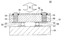
- the semiconductor device 50 includes an Al through a through electrode 56.
- the electrode pad 55 and the rewiring pattern 52 are connected, and the rewiring pattern 52 of the semiconductor device and the rewiring pattern 57 on the wiring board 53 are connected via the solder bumps 58.
- a device formation layer 59 and a plurality of Al electrode pads 55 are formed on the upper surface of the semiconductor device.
- a through hole 54 penetrating the semiconductor device is provided between the Al electrode pad 55 and the rewiring pattern 52 by dry etching, and a through electrode 56 is formed in the through hole 54 by Cu plating.
- the device formation layer 59 is disposed on the upper surface of the semiconductor device and receives light or emits light. According to this method, the semiconductor element 51 and the wiring substrate 53 are not bonded by wire bonding, but rewiring must be performed on the semiconductor device and solder bumps must be disposed. In reality, it is difficult to achieve finer wiring and higher density solder bumps.
- Patent Document 2 discloses a manufacturing method of a semiconductor device useful for three-dimensional stacking of a plurality of semiconductor elements.
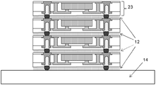
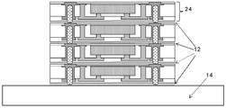
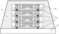
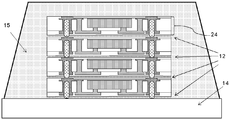
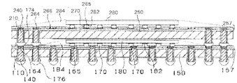
- a structure in which a semiconductor element 180 and a semiconductor element 280 are stacked is shown. Illustrated.
- Each semiconductor element to be laminated includes solder bumps (170, 270) on a substrate (110, 210) having a core substrate (150, 250), through electrodes (140, 240), and wiring layers (157, 257).
- the semiconductor element (180, 280) is bonded via the pad (182, 282) of the semiconductor element.
- the wiring layers (157, 257) include mounting pads (165, 265), connection pads (164, 264), and wiring (266).
- Patent Document 2 discloses a method of bonding and laminating substrates on which such semiconductor elements are bonded via solder bumps (174, 176).
- Patent Document 2 since the semiconductor element is bonded to the wiring board by solder bumps, as in Patent Document 1, it is extremely important to increase the density of the solder bumps accompanying the downsizing of the semiconductor elements. You will face difficulties.
- the formation of the through electrode provided on the second substrate 210 has a problem that the process is complicated and not easy.
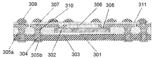
- Patent Document 3 shows an example of a semiconductor device mounted on a wiring board, a manufacturing method thereof, or a semiconductor device in which semiconductor elements are assembled in a laminated structure, and a manufacturing method thereof.
- Patent Document 3 as shown in FIG. 27, an organic substrate 301, a through via 304 that penetrates the organic substrate 301 in the thickness direction, and an external portion that is provided on both surfaces of the organic substrate 301 and is electrically connected to the through via 304.
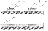
- Patent Document 3 as shown in FIG. 28, a photosensitive resin layer 316 applied to the surface layer of a semiconductor element is patterned to form an opening 317, whereby a via portion 308 formed on the semiconductor element 302 is formed. And Further, the insulating material layer 306 formed around the semiconductor element is formed by spin coating or the like.
- the resin since the resin has to be supplied twice, the process of applying the photosensitive resin layer 316 to the surface layer of the semiconductor element 302 and the process of forming the insulating material layer 306 around the semiconductor element 302, the process is complicated.
- the height of the semiconductor element 302 is important, and when the height exceeds tens of ⁇ m, the semiconductor element is overcome and a void is generated. It is actually difficult to supply the insulating material layer 306.
- the formation of the via portion 308 of the photosensitive resin layer 316 and the formation of the metal via 310 of the insulating material layer 306 are performed in separate processes, and an example in which the processing of the metal via 310 is performed by a laser or the like are shown. These processes are cumbersome and unreasonable.
- the photosensitive resin layer 316 and the insulating material layer 306 can be simultaneously supplied to the peripheral portion of the semiconductor element 302 and the circuit formation surface, there is actually no specific method illustrated, and a gap is formed around the semiconductor element. It is difficult to supply these resin layers without generating them.
- the via portion 308 of the photosensitive resin layer 316 and the metal via 310 of the insulating material layer 306 can be formed at the same time, a specific method is not described.
- the present invention has been made in view of the above circumstances, and provides a semiconductor device that can be easily placed on a wiring board and stacked on a semiconductor device, and the warpage of the semiconductor device is suppressed even when the density of the metal wiring is large. With the goal. It is another object of the present invention to provide a method for manufacturing a semiconductor device, which can easily process a through electrode and an opening of an electrode pad portion when manufacturing such a semiconductor device. It is another object of the present invention to provide a stacked semiconductor device in which such semiconductor devices are stacked, a post-sealing stacked semiconductor device in which the semiconductor device is mounted on a wiring board and sealed, and a method for manufacturing the same.
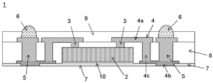
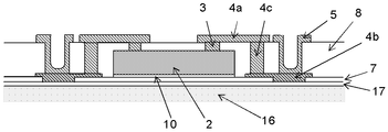
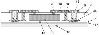
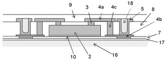
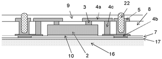
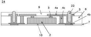
- the present invention has a semiconductor element, a metal pad on the semiconductor element and a metal wiring electrically connected to the semiconductor element, and the metal wiring is electrically connected to the through electrode and the solder bump.
- the metal wiring is electrically connected to the semiconductor element through a metal pad on the semiconductor element on the upper surface of the second insulating layer, and penetrates the second insulating layer from the upper surface of the second insulating layer.
- a semiconductor device electrically connected to the through electrode on the lower surface of a second insulating layer is provided.
- the first insulating layer is formed by a photocurable dry film or a photocurable resist coating film
- the second insulating layer is formed by the photocurable dry film
- the third insulating layer is preferably formed of the photocurable dry film or the photocurable resist coating film.
- the height of the semiconductor element is 20 to 100 ⁇ m
- the thickness of the first insulating layer is 1 to 20 ⁇ m
- the thickness of the second insulating layer is 5 to 100 ⁇ m
- the insulating layer has a thickness of 5 to 100 ⁇ m
- the semiconductor device has a thickness of 50 to 300 ⁇ m.
- the photo-curable dry film is (A) a silicone skeleton-containing polymer compound having a repeating unit represented by the following general formula (1) and having a weight average molecular weight of 3,000 to 500,000, (Wherein R 1 to R 4 represent a monovalent hydrocarbon group having 1 to 8 carbon atoms which may be the same or different.
- M is an integer of 1 to 100.
- a, b, c and d are 0. Or, a positive number and a, b, c, and d are not simultaneously 0.
- a + b + c + d 1
- X is an organic group represented by the following general formula (2)
- Y is the following general formula.
- Z is A divalent organic group selected from any one of the following: n is 0 or 1; R 5 and R 6 are each an alkyl group or alkoxy group having 1 to 4 carbon atoms, and may be different or the same. k is 0, 1, or 2.
- R 5 and R 6 are each an alkyl group or alkoxy group having 1 to 4 carbon atoms, and may be different or the same.
- k is 0, 1, or 2.
- R 7 and R 8 are each an alkyl group or alkoxy group having 1 to 4 carbon atoms, and may be different or the same.
- h is 0, 1, or 2.
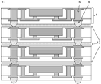
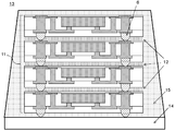
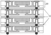
- the present invention also provides a stacked semiconductor device in which a plurality of the above semiconductor devices are flip-chip stacked. Since the semiconductor device of the present invention can be easily stacked, it is suitable for such a stacked semiconductor device.
- the present invention provides a post-sealing laminated semiconductor device in which the laminated semiconductor device is placed on a substrate having an electric circuit and sealed with an insulating sealing resin layer.
- the semiconductor device of the present invention is suitable for such a post-sealing stacked semiconductor device because it is easy to mount the semiconductor device on a wiring board and to stack the semiconductor devices.
- a method of manufacturing a semiconductor device (1) applying a temporary adhesive to the support substrate, and forming a first insulating layer having a thickness of 1 to 20 ⁇ m using the resist composition material as a photocurable resin layer on the temporary adhesive; (2) The step of patterning the first insulating layer by lithography through a mask to form a hole pattern to be a through electrode and then baking the first insulating layer by baking; (3) performing a seed layer formation by sputtering on the first insulating layer, then filling the hole pattern to be the through electrode by plating, and forming a metal wiring connected to the through electrode; (4) a step of die-bonding a semiconductor element having a height of 20 to 100 ⁇ m with an electrode pad exposed on the upper surface using a die-bonding agent on the cured first insulating layer; (5) A photocurable dry film having a structure in which a photocurable resin layer having a film thickness of 5 to 100 ⁇ m is sandwiched between a support film and
- the second insulating layer is patterned by lithography through a mask, and the metal penetrates the second insulating layer over the opening on the electrode pad and the metal wiring connected to the through electrode.
- a seed layer is formed by sputtering, and thereafter an opening on the electrode pad, an opening for forming a metal wiring penetrating the second insulating layer, and an opening for forming the through electrode Is embedded by plating to form a metal pad on the semiconductor element, a metal wiring penetrating the second insulating layer, and a through electrode, and the metal pad on the semiconductor element and the second insulation formed by the plating.
- the third insulating layer is formed by laminating the photocurable resin layer of the photocurable dry film or spin-coating the resist composition material used for the photocurable dry film. And a process of (10) The third insulating layer is patterned by lithography through a mask, an opening is formed in the upper portion of the through electrode, and then the third insulating layer is cured by baking; (11) A step of forming a solder bump in the opening above the through electrode after curing, The manufacturing method of the semiconductor device which has this.
- the photocurable dry film prepared in the step (5) contains (A) a silicone skeleton containing a repeating unit represented by the following general formula (1) and having a weight average molecular weight of 3,000 to 500,000.
- M is an integer of 1 to 100.
- X is an organic group represented by the following general formula (2), and Y is the following general formula.
- Z is A divalent organic group selected from any one of the following: n is 0 or 1; R 5 and R 6 are each an alkyl group or alkoxy group having 1 to 4 carbon atoms, and may be different or the same. k is 0, 1, or 2.
- R 5 and R 6 are each an alkyl group or alkoxy group having 1 to 4 carbon atoms, and may be different or the same.
- k is 0, 1, or 2.
- R 7 and R 8 are each an alkyl group or alkoxy group having 1 to 4 carbon atoms, and may be different or the same.
- h is 0, 1, or 2.
- the step (6) preferably includes a step of mechanically pressing the second insulating layer. Thereby, the thickness of the 2nd insulating layer on a semiconductor element can be made thin, it can equalize, and a 2nd insulating layer can be planarized.
- the solder bump can be formed in the opening above the through electrode.
- the step of plating with SnAg In the step (10), exposing the plated SnAg by patterning so as to form an opening above the through electrode; In the step (11), a step of forming a solder bump by raising the electrode in the opening above the through electrode by melting the plated SnAg, If it is the method which has this, a solder bump can be formed in the opening of the said penetration electrode more easily and rationally.
- step (11) a step of removing the support substrate temporarily bonded to the first insulating layer in the step (1); After removing the substrate, the step of dicing into pieces, By performing the above, it is possible to manufacture an individual semiconductor device.
- the following effects can be imparted. That is, when the periphery of the semiconductor element placed on the first insulating layer formed on the support substrate is embedded with a photocurable dry film using a resist composition material as a photocurable resin layer, a photocurable resin is used. Since the layer has a thickness of 5 to 100 ⁇ m, even when the height of the semiconductor element is several tens of ⁇ m, it becomes possible to embed a photocurable dry film without generating voids around the semiconductor element. Easy.
- the light on the semiconductor device By mechanically pressing the curable resin layer (second insulating layer), it has the advantage that the film thickness can be adjusted and thinned, and the mechanical press is a photocurable resin laminated on the outer periphery of the semiconductor element. It has the advantage that the layer thickness can be made uniform and flat.
- an opening on the electrode pad on the semiconductor element, an opening for forming a metal wiring penetrating the second insulating layer, and an opening to be a through electrode Can be simultaneously formed by patterning by lithography through a mask.
- TMV Through Metal Via
- the opening on the electrode pad on the semiconductor element, the opening for forming the metal wiring penetrating the second insulating layer, and the opening for forming the through electrode are filled by plating, and the metal pad on the semiconductor element and the second insulating layer By laminating a photo-curable dry film on the metal wiring that penetrates the metal element and the through electrode, and the metal wiring that penetrates the metal pad on the semiconductor element and the second insulating layer is metal-plated by plating.
- the method of separating the support substrate after removing it is a method by which a semiconductor device can be easily manufactured.
- a step of plating with SnAg is included, and a lamination is performed again by laminating a photo-curable dry film. After performing patterning to form an opening in the upper part, after exposing the SnAg plating, and after patterning and curing the film by baking, the SnAg filled by plating is melted to open the through electrode opening. Providing a way to raise.
- the first insulating layer formed on the support substrate is bonded to the support substrate with a temporary adhesive, and then the support substrate is easily removed, and the support substrate is removed and then diced to remove the support substrate. It is easy and reasonable to manufacture an individual semiconductor device.
- the upper part protrudes a solder ball or a solder bump which is a raised SnAg, and the lower part can easily expose the through electrode by removing the substrate. It is very rational because it can be easily electrically joined and stacked using solder bumps and exposed electrodes protruding from a plurality of separated semiconductor devices.
- the warpage of the semiconductor device itself tends to increase as the wiring density increases.
- metal wiring By forming metal wiring on both surfaces of the insulating layer, warpage of the semiconductor device itself can be suppressed even if the wiring density increases.
- multilayer wiring will be required to cope with the increase in the number of signals in the semiconductor device. Therefore, it is important to minimize the warpage of the semiconductor device itself.
- the semiconductor device of the present invention provided with wiring can be extremely reduced in warpage, and thus is suitable for multilayer wiring.
- the chemically amplified negative resist composition material in the present invention is used for the photocurable resin layer, it is possible to reduce the warpage of the semiconductor device which is a concern when separated into individual pieces. It is suitable for mounting on a wiring board.
- a fine electrode is formed on a semiconductor element, and a through electrode is provided outside the semiconductor element, so that the semiconductor device can be placed on a wiring board or stacked on the semiconductor device.
- the semiconductor element is embedded without voids around the semiconductor element, and even when the density of the metal wiring is high, the semiconductor device can be prevented from warping.
- a fine electrode is formed on a semiconductor element, and a through electrode is provided on the outside of the semiconductor element, so that mounting on a wiring board and stacking of semiconductor devices can be easily performed.
- the semiconductor device of the present invention can be easily mounted on a wiring board and stacked on the wiring board, a stacked semiconductor device in which semiconductor devices are stacked and the semiconductor board mounted on the wiring board are mounted. It is possible to obtain a stacked semiconductor device after sealing which is placed and sealed.
- a first insulating layer is formed using a resist composition material on a support substrate coated with a temporary adhesive, and the first insulating layer is patterned to form a hole pattern to be a through electrode.
- a hole pattern to be a through electrode is filled by plating to form a metal wiring connected to the through electrode, and a semiconductor element is die-bonded on the first insulating layer.
- the film is embedded without generating voids around the semiconductor element. (Formation of the second insulating layer).
- an opening on the electrode pad, an opening for forming a metal wiring penetrating the second insulating layer, and a through electrode are formed. Since it was possible to form the openings simultaneously, it was found that they could be easily processed, and the present invention was achieved.
- the opening on the electrode pad, the opening for forming the metal wiring penetrating the second insulating layer, and the opening for forming the through electrode are plated.
- the metal pad on the semiconductor element, the metal wiring penetrating the second insulating layer, and the penetrating electrode are formed, and the metal pad penetrating the semiconductor element on the semiconductor element and the metal wiring penetrating the second insulating layer are formed by plating. Connected by metal wiring by plating.
- a third insulating layer is formed from above, and patterning is performed on the third insulating layer to form an opening above the through electrode, and after curing, a solder bump is formed in this opening.
- removing the support substrate that has been bonded with the temporary adhesive and dividing it into individual pieces by dicing is a very rational method for forming a semiconductor device and embodies the object of the present invention. .
- the semiconductor device manufactured by the above manufacturing method can suppress warping of the semiconductor device itself even when the wiring density is increased by forming metal wiring on both surfaces of the second insulating layer.
- the semiconductor device manufactured by the above manufacturing method has a solder bump that protrudes from the plurality of semiconductor devices because the solder bumps protrude from the upper part, and the through electrode can be easily exposed by removing the support substrate from the lower part.
- the exposed electrodes the inventors have found that they can be easily electrically joined and stacked, and have found that the stacked semiconductor devices can be easily placed on a wiring board, thereby completing the present invention.
- the present invention has a semiconductor device, a semiconductor device having a metal pad and a metal wiring on the semiconductor element electrically connected to the semiconductor element, and the metal wiring is electrically connected to the through electrode and the solder bump. Because A first insulating layer on which the semiconductor element is placed; a second insulating layer formed on the semiconductor element; and a third insulating layer formed on the second insulating layer; The metal wiring is electrically connected to the semiconductor element through a metal pad on the semiconductor element on the upper surface of the second insulating layer, and penetrates the second insulating layer from the upper surface of the second insulating layer. In the semiconductor device, the lower surface of the second insulating layer is electrically connected to the through electrode.
- the semiconductor device 1 of the present invention includes a semiconductor element 2, a semiconductor element upper metal pad 3 and a metal wiring 4 electrically connected to the semiconductor element 2, and the metal wiring 4 is a through electrode. 5 and a solder bump 6, which are electrically connected to the semiconductor device 2, a first insulating layer 7 on which the semiconductor element 2 is placed, a second insulating layer 8 formed on the semiconductor element 2, and a second A third insulating layer 9 formed on the insulating layer 8;
- the metal wiring 4 is electrically connected to the semiconductor element 2 via the metal pad 3 on the semiconductor element on the upper surface of the second insulating layer 8, and penetrates the second insulating layer 8 from the upper surface of the second insulating layer 8.
- the semiconductor device is electrically connected to the through electrode 5 on the lower surface of the two insulating layers 8.
- the metal wiring 4 is a metal wiring (upper surface metal wiring) 4 a connected to the semiconductor element upper metal pad 3 on the upper surface of the second insulating layer 8, and a metal connected to the through electrode 5 on the lower surface of the second insulating layer 8.
- the wiring (bottom metal wiring) 4b and the metal wiring (through metal wiring) 4c that penetrates the second insulating layer 8 and connects the top metal wiring 4a and the bottom metal wiring 4b.
- the semiconductor element 2 is die-bonded to the first insulating layer 7 with a die bonding agent 10.
- the first insulating layer 7 is formed of a photocurable dry film or a photocurable resist coating film
- the second insulating layer 8 is formed of a photocurable dry film. If the three insulating layers 9 are formed of a photocurable dry film or a photocurable resist coating film, even if the height of the semiconductor element 2 is several tens of ⁇ m, it is embedded without any voids around the semiconductor element. Therefore, it is preferable.
- the height of the semiconductor element 2 is 20 to 100 ⁇ m
- the thickness of the first insulating layer 7 is 1 to 20 ⁇ m
- the thickness of the second insulating layer 8 is 5 to 100 ⁇ m
- the thickness of the layer 9 is 5 to 100 ⁇ m
- the thickness of the semiconductor device 1 is 50 to 300 ⁇ m, it is preferable that the semiconductor device 1 is embedded without voids around the semiconductor element and becomes a thin semiconductor device.
- the photocurable dry film used for forming the first insulating layer 7, the second insulating layer 8, and the third insulating layer 9 suppresses warpage, reduces residual stress, reliability, and processing characteristics.
- a photocurable dry film having a photocurable resin layer composed of a chemically amplified negative resist composition material containing the following components (A) to (D) is preferable.
- other photosensitive resins can also be used.
- the component (A) is a silicone skeleton-containing polymer compound having a repeating unit represented by the following general formula (1) and having a weight average molecular weight of 3,000 to 500,000.
- R 1 to R 4 represent a monovalent hydrocarbon group having 1 to 8 carbon atoms which may be the same or different.
- M is an integer of 1 to 100.
- a, b, c and d are 0. Or, a positive number and a, b, c, and d are not simultaneously 0.
- a + b + c + d 1
- X is an organic group represented by the following general formula (2)
- Y is the following general formula.
- Z is A divalent organic group selected from any one of the following: n is 0 or 1; R 5 and R 6 are each an alkyl group or alkoxy group having 1 to 4 carbon atoms, and may be different or the same. k is 0, 1, or 2.
- R 5 and R 6 are each an alkyl group or alkoxy group having 1 to 4 carbon atoms, and may be different or the same.
- k is 0, 1, or 2.
- R 7 and R 8 are each an alkyl group or alkoxy group having 1 to 4 carbon atoms, and may be different or the same.
- h is 0, 1, or 2.
- Component (B) is an amino condensate modified with formaldehyde or formaldehyde-alcohol, one or two or more selected from phenol compounds having an average of two or more methylol groups or alkoxymethylol groups in one molecule. It is a crosslinking agent.
- Component (C) is a photoacid generator that decomposes with light having a wavelength of 190 to 500 nm to generate an acid.
- a component is a solvent.
- crosslinking agent for the component (B) known ones can be used.
- 1 type (s) or 2 or more types chosen from the phenolic compound which has group can be used.
- amino condensate modified with formaldehyde or formaldehyde-alcohol examples include melamine condensate modified with formaldehyde or formaldehyde-alcohol, or urea condensate modified with formaldehyde or formaldehyde-alcohol. These modified melamine condensates and modified urea condensates can be used alone or in combination.
- phenol compound having an average of two or more methylol groups or alkoxymethylol groups in one molecule examples include (2-hydroxy-5-methyl) -1,3-benzenedimethanol, 2,2 ′, Examples include 6,6′-tetramethoxymethylbisphenol A.
- these phenol compounds can be used 1 type or in mixture of 2 or more types.
- an acid generator which generates an acid upon irradiation with light having a wavelength of 190 to 500 nm and becomes a curing catalyst can be used.
- photoacid generators include onium salts, diazomethane derivatives, glyoxime derivatives, ⁇ -ketosulfone derivatives, disulfone derivatives, nitrobenzyl sulfonate derivatives, sulfonate ester derivatives, imido-yl-sulfonate derivatives, oxime sulfonate derivatives, iminosulfonates. Derivatives, triazine derivatives and the like.
- a solvent in which (A) a silicone skeleton-containing polymer compound, (B) a crosslinking agent, and (C) a photoacid generator can be dissolved can be used.
- solvents include ketones such as cyclohexanone, cyclopentanone, and methyl-2-n-amyl ketone; 3-methoxybutanol, 3-methyl-3-methoxybutanol, 1-methoxy-2-propanol, 1- Alcohols such as ethoxy-2-propanol; ethers such as propylene glycol monomethyl ether, ethylene glycol monomethyl ether, propylene glycol monoethyl ether, ethylene glycol monoethyl ether, propylene glycol dimethyl ether, diethylene glycol dimethyl ether; propylene glycol monomethyl ether acetate, propylene Glycol monoethyl ether acetate, ethyl lactate, ethyl
- the first insulating layer 7 and the third insulating layer 9 are photo-curable resists obtained by applying a chemically amplified negative resist composition material containing the above components (A) to (D) by spin coating or the like. It may be a coating film or, of course, a photocurable resist coating film in which another photosensitive resin is applied by spin coating or the like.
- the present invention provides a stacked semiconductor device in which a plurality of the above semiconductor devices are flip-chip stacked.
- the stacked semiconductor device 11 of the present invention is a device in which the above-described semiconductor device 1 is flip-chiped and electrically joined by the through electrode 5 and the solder bump 6, and a plurality of stacked layers are stacked.
- An insulating resin layer 12 may be sealed between the semiconductor devices.
- the present invention provides a post-sealing laminated semiconductor device in which the laminated semiconductor device is placed on a substrate having an electric circuit and sealed with an insulating sealing resin layer.
- the post-sealing laminated semiconductor device 13 of the present invention is mounted on the substrate (wiring substrate 14) having the electric circuit described above via the solder bumps 6 as shown in FIG. And sealed with an insulating sealing resin layer 15.
- a method for manufacturing a semiconductor device of the present invention includes: (1) applying a temporary adhesive to the support substrate, and forming a first insulating layer having a thickness of 1 to 20 ⁇ m using the resist composition material as a photocurable resin layer on the temporary adhesive; (2) The step of patterning the first insulating layer by lithography through a mask to form a hole pattern to be a through electrode and then baking the first insulating layer by baking; (3) performing a seed layer formation by sputtering on the first insulating layer, then filling the hole pattern to be the through electrode by plating, and forming a metal wiring connected to the through electrode; (4) a step of die-bonding a semiconductor element having a height of 20 to 100 ⁇ m with an electrode pad exposed on the upper surface using a die-bonding agent on the cured first insulating layer; (5) A photocurable dry film having a structure in which a photocurable resin layer having
- the second insulating layer is patterned by lithography through a mask, and the metal penetrates the second insulating layer over the opening on the electrode pad and the metal wiring connected to the through electrode.
- a seed layer is formed by sputtering, and thereafter an opening on the electrode pad, an opening for forming a metal wiring penetrating the second insulating layer, and an opening for forming the through electrode Is embedded by plating to form a metal pad on the semiconductor element, a metal wiring penetrating the second insulating layer, and a through electrode, and the metal pad on the semiconductor element and the second insulation formed by the plating.
- the third insulating layer is formed by laminating the photocurable resin layer of the photocurable dry film or spin-coating the resist composition material used for the photocurable dry film. And a process of (10) The third insulating layer is patterned by lithography through a mask, an opening is formed in the upper portion of the through electrode, and then the third insulating layer is cured by baking; (11) A step of forming a solder bump in the opening above the through electrode after curing, Have
- step (1) as shown in FIG. 4, a temporary adhesive 17 is applied to the support substrate 16, and a resist composition material is used as a photocurable resin layer on the temporary adhesive 17 to obtain a film thickness of 1 to 1.
- a 20 ⁇ m first insulating layer 7 is formed.
- the support substrate 16 For example, a silicon wafer, a glass substrate, etc. can be used.
- the temporary adhesive 17 is not particularly limited, but for example, a thermoplastic resin is preferable. Examples include olefin-based thermoplastic elastomers, polybutadiene-based thermoplastic elastomers, styrene-based thermoplastic elastomers, styrene-butadiene-based thermoplastic elastomers, and styrene-polyolefin-based thermoplastic elastomers. Is preferred.
- the first insulating layer 7 is, for example, a photocurable dry layer having a photocurable resin layer made of a chemically amplified negative resist composition material containing the components (A) to (D). It can be formed by laminating using a film or by applying the resist composition material by spin coating or the like. Of course, other photosensitive resins can also be used.
- the film thickness of the first insulating layer is 1 to 20 ⁇ m, preferably 5 to 10 ⁇ m. Such a film thickness is preferable because the semiconductor device to be manufactured can be thinned.
- the first insulating layer 7 is patterned by lithography through a mask, and a hole pattern A to be a through electrode is formed as shown in FIG.
- the insulating layer 7 is cured.
- a pattern can be formed using a known lithography technique.
- preheating may be performed as necessary.
- Pre-baking can be performed, for example, at 40 to 140 ° C. for about 1 minute to 1 hour.
- the film is exposed to light with a wavelength of 190 to 500 nm through a photomask and cured.
- the photomask may be formed by cutting a desired pattern.
- the material of the photomask is preferably a material that shields light having a wavelength of 190 to 500 nm.
- chromium is preferably used, but is not limited thereto.
- Examples of light having a wavelength of 190 to 500 nm include light of various wavelengths generated by a radiation generator, for example, ultraviolet light such as g-line and i-line, deep ultraviolet light (248 nm, 193 nm), and the like.
- the wavelength is preferably 248 to 436 nm.
- the exposure dose is preferably 10 to 3,000 mJ / cm 2 , for example.
- PEB is performed to increase the development sensitivity.
- PEB can be, for example, at 40 to 140 ° C. for 0.5 to 10 minutes.
- a preferred developer includes an organic solvent such as IPA or PGMEA.
- a preferred alkaline aqueous developer is, for example, a 2.38% tetramethylhydroxyammonium (TMAH) aqueous solution.
- TMAH tetramethylhydroxyammonium
- an organic solvent is preferably used as the developer. Development can be performed by a normal method, for example, by immersing a substrate on which a pattern is formed in a developer. Thereafter, washing, rinsing, drying, and the like are performed as necessary to obtain a film (first insulating layer) of the photocurable resin layer having a desired pattern.
- the first insulating layer thus patterned is baked using an oven or a hot plate, preferably at a temperature of 100 to 250 ° C., more preferably 150 to 220 ° C., and even more preferably 170 to 190 ° C. And cured (post-curing). If the post-curing temperature is 100 to 250 ° C., the crosslink density of the first insulating layer can be increased and the remaining volatile components can be removed, which is preferable from the viewpoint of adhesion to the support substrate, heat resistance and strength, and electrical characteristics.
- the post-curing time can be 10 minutes to 10 hours.
- step (3) a seed layer is formed on the first insulating layer 7 by sputtering, and then the hole pattern A to be a through electrode is filled by plating, and the metal connected to the through electrode as shown in FIG. Wiring (lower surface metal wiring) 4b is formed.
- the lower surface metal wiring 4b is formed. After forming the metal wiring, the seed layer is removed by etching, and the first insulating layer 7 is exposed.
- the lower surface metal wiring 4b may be appropriately adjusted to have a desired wiring width, but is preferably formed on the first insulating layer so as to have a thickness of 0.1 to 10 ⁇ m.
- step (4) as shown in FIG. 7, the semiconductor element 2 having a height of 20 to 100 ⁇ m with the electrode pad exposed on the upper surface is applied onto the cured first insulating layer 7 with the die bonding agent 10.
- the die bonding agent 10 may be a known adhesive. Further, it is preferable that the height of the semiconductor element 2 is 20 to 100 ⁇ m because the semiconductor device to be manufactured can be thinned.
- a photocurable resin layer having a film thickness of 5 to 100 ⁇ m has a structure sandwiched between a support film and a protective film, and the photocurable resin layer is a light comprising a resist composition material.
- the photocurable resin layer is a light comprising a resist composition material.
- the photocurable dry film used for this invention has a structure in which a photocurable resin layer having a thickness of 5 to 100 ⁇ m is sandwiched between a support film and a protective film. And the photocurable resin layer is made of a resist composition material.
- the thickness of the photocurable resin layer of the photocurable dry film used for forming the second insulating layer is 5 to 100 ⁇ m. This is preferable because the semiconductor device to be manufactured can be thinned. In addition, what is necessary is just to prepare and use what made the film thickness of the photocurable resin layer arbitrary, when using a photocurable dry film for formation of a 1st insulating layer and a 3rd insulating layer.
- each component of the composition of the photosensitive material is stirred and mixed, and then filtered through a filter or the like to prepare a resist composition material for forming a photocurable resin layer.
- a resist composition material a chemically amplified negative resist composition material containing the above-described components (A) to (D) is suitable.
- other photosensitive resins can also be used.
- the support film used in the photocurable dry film used in the present invention may be a single film or a multilayer film in which a plurality of polymer films are laminated.
- the dry film is a film sandwiched between a support film and a protective film.
- the material of the support film include synthetic resin films such as polyethylene, polypropylene, polycarbonate, and polyethylene terephthalate, and polyethylene terephthalate having appropriate flexibility, mechanical strength, and heat resistance is preferable. Further, these films may be subjected to various treatments such as corona treatment or a release agent.
- the protective film used in the photocurable dry film used in the present invention may be the same as the above-described support film, but polyethylene terephthalate and polyethylene having moderate flexibility are preferable. Commercially available products can be used. Examples of polyethylene terephthalate include those already exemplified, and examples of polyethylene include GF-8 (manufactured by Tamapoly Co., Ltd.) and PE film 0 type (manufactured by Nipper Co., Ltd.). .
- the thicknesses of the support film and the protective film are preferably 5 to 100 ⁇ m from the viewpoints of the stability of photocurable dry film production and curling against the winding core, so-called curling prevention.
- a film coater for producing a pressure-sensitive adhesive product can be used as the photocurable dry film production apparatus.
- the film coater include a comma coater, a comma reverse coater, a multi coater, a die coater, a lip coater, a lip reverse coater, a direct gravure coater, an offset gravure coater, a three bottom reverse coater, and a four bottom reverse coater. It is done.
- a resist composition material is applied with a predetermined thickness on the support film to form a photocurable resin layer
- a photocurable resin layer that has been passed through a hot-air circulating oven at a predetermined temperature and a predetermined time and dried on a support film is laminated at a predetermined pressure together with a protective film that has been unwound from another unwinding shaft of the film coater.
- the film is manufactured by passing the roll and pasting it with the photocurable resin layer on the support film, and then winding it on the winding shaft of the film coater.
- the temperature of the hot air circulating oven is preferably 25 to 150 ° C.
- the passage time is preferably 1 to 100 minutes
- the pressure of the laminate roll is preferably 0.01 to 5 MPa.
- a photocurable dry film can be produced by the above-described method, and by using such a photocurable dry film, a semiconductor element placed on the first insulating layer on the support substrate is embedded. It has excellent characteristics and can relieve stress that occurs when the support substrate is removed after the semiconductor device is formed or when the semiconductor device is separated. It is suitable for stacking or mounting on a substrate provided with wiring.
- step (6) the protective film is peeled off from the photocurable dry film prepared as described above, and the semiconductor die-bonded onto the first insulating layer 7 as shown in FIG. 8 (a).
- a second insulating layer 8 is formed by laminating a photocurable resin layer of a photocurable dry film so as to cover the element 2.
- a vacuum laminator is preferable as an apparatus for attaching the photocurable dry film. Attach a photocurable dry film to the device, peel off the protective film of the photocurable dry film and expose the exposed photocurable resin layer in a vacuum chamber with a predetermined degree of vacuum, using an adhesive roll with a predetermined pressure, The substrate is brought into close contact with the substrate at a predetermined temperature.
- the temperature is preferably 60 to 120 ° C.
- the pressure is preferably 0 to 5.0 MPa
- the vacuum is preferably 50 to 500 Pa. It is preferable to perform vacuum laminating without generating voids around the semiconductor element.
- the film thickness of the second insulating layer 8 on the semiconductor element 2 may gradually decrease as the distance from the semiconductor element 2 increases.
- a method of flattening by mechanically pressing the change in the film thickness and reducing the film thickness on the semiconductor element as shown in FIG. 8A can be preferably used.
- step (7) as shown in FIG. 9, the second insulating layer 8 is patterned by lithography through a mask, and the metal connected to the opening B on the electrode pad and the through electrode is formed. Baking after simultaneously forming an opening C for forming a metal wiring (through metal wiring) penetrating the second insulating layer and an opening D for forming a through electrode on the wiring (lower surface metal wiring) 4b. Then, the second insulating layer 8 is cured.
- a pattern can be formed using a known lithography technique and may be performed by the same method as the patterning of the first insulating layer.
- the opening B on the electrode pad, the opening C for forming the through metal wiring, and the opening D for forming the through electrode are simultaneously formed by collective exposure. Is.
- step (8) as shown in FIG. 10, after the second insulating layer 8 is cured, a seed layer is formed by sputtering, and then the opening B on the electrode pad and the metal penetrating the second insulating layer are formed.
- the opening C for forming the wiring (through metal wiring) and the opening D for forming the through electrode are filled by plating, and the metal wiring (through metal) penetrating the semiconductor element upper metal pad 3 and the second insulating layer.
- (Wiring) 4c and through electrode 5 are formed, and metal wiring (through metal wiring) 4c penetrating through the metal pad 3 on the semiconductor element and the second insulating layer formed by plating and metal wiring (upper surface metal wiring) by plating is formed. ) Connect with 4a.
- step (3) When performing plating, as in the above-described step (3), for example, after forming a seed layer by sputtering, patterning of a plating resist is performed, followed by electrolytic plating, The through metal wiring 4c and the through electrode 5 are formed, and the upper surface metal wiring 4a is formed to connect the semiconductor element upper metal pad 3 and the through metal wiring 4c.
- the upper surface metal wiring 4a may be appropriately adjusted so as to have a desired wiring width, but is preferably formed on the second insulating layer so as to have a thickness of 0.1 to 10 ⁇ m.
- the through electrode 5 may be separately subjected to electrolytic plating, and the through electrode 5 may be filled with the metal plating 18. Further, in order to satisfy the plating of the through metal wiring 4c, the through metal wiring 4c may be separately subjected to electrolytic plating again.
- step (9) after forming the metal wiring, the photocurable resin layer of the photocurable dry film is laminated, or the resist composition material used for the photocurable dry film is spin-coated. As shown in FIG. 12, the third insulating layer 9 is formed.
- the formation of the third insulating layer 9 is similar to the formation of the first insulating layer described above, for example, a photocurable resin made of a chemically amplified negative resist composition material containing components (A) to (D). Lamination can be performed using a photocurable dry film having a layer, or the resist composition material can be applied by spin coating or the like. Of course, other photosensitive resins can also be used. A thickness of the third insulating layer of 5 to 100 ⁇ m is preferable because the semiconductor device to be manufactured can be thinned.
- step (10) the third insulating layer 9 is patterned by lithography through a mask to form an opening E above the through electrode 5 and then baked.
- the third insulating layer 9 is cured.
- a pattern can be formed using a known lithography technique and may be performed by the same method as the patterning of the first insulating layer.
- a solder bump is formed in the opening E above the through electrode.
- a method for forming a solder bump for example, as shown in FIG. 14, a metal pad 19 on the through electrode is formed in the opening E above the through electrode by plating.
- a solder ball 20 can be formed on the through electrode upper metal pad 19 and used as a solder bump.
- step (8) a separate plating for satisfying the plating of the through electrode 5 is performed with SnAg and the SnAg plating 21 is performed, and in the subsequent step (9), the same as the above In step (10), the third insulating layer 9 is formed, and the SnAg plating 21 is exposed by patterning so as to form the opening E above the through electrode in step (10), followed by curing by baking, as step (11).
- the electrode By melting the SnAg plating 21, the electrode can be raised to the opening E above the through electrode as shown in FIG. 16, and the solder bump of the electrode 22 with the raised SnAg can be formed.
- the solder ball 20 of the through electrode 5 is removed. Can be exposed, the exposed seed layer is removed by etching, and the metal plating portion is exposed, whereby the upper and lower portions of the through electrode 5 can be electrically connected. it can. Further, the semiconductor device 23 can be obtained by dicing into individual pieces.
- the support substrate 16 is removed as shown in FIG.
- the metal wiring 4b) can be exposed, the exposed seed layer is removed by etching, and the metal plating portion is exposed, whereby the upper and lower portions of the through electrode 5 can be electrically connected. Furthermore, after that, the semiconductor device 24 separated into pieces can be obtained by dicing into pieces.
- the manufacturing method of the present invention as described above is particularly suitable for downsizing and thinning, and a thin and compact semiconductor device having a thickness of 50 to 300 ⁇ m, more preferably 70 to 150 ⁇ m as a semiconductor device. Can be obtained.
- the above-described individual semiconductor device 23 or individual semiconductor device 24 is electrically joined by solder bumps with the insulating resin layer 12 interposed therebetween.
- a stacked semiconductor device can be obtained by stacking.
- the stacked semiconductor devices can be mounted on a substrate (wiring substrate 14) having an electric circuit.
- 19, 20, 21, and 22 are examples of flip-chip bonding of individual semiconductor devices 23 or 24.
- Type semiconductor device can be manufactured.
- the resin used for the insulating resin layer 12 and the insulating sealing resin layer 15 can be used, and for example, epoxy resins, silicone resins, and hybrid resins thereof can be used. .
- the semiconductor device, stacked semiconductor device, and post-sealing stacked semiconductor device of the present invention manufactured as described above are suitable for fan-out wiring and WCSP (wafer level chip size package) applied to a semiconductor chip. Can be used.
- WCSP wafer level chip size package
- a fine electrode is formed on a semiconductor element, and a through electrode is provided outside the semiconductor element, so that the semiconductor device can be placed on a wiring board or stacked on the semiconductor device.
- the semiconductor element is embedded without voids around the semiconductor element, and even when the density of the metal wiring is high, the semiconductor device can be prevented from warping.
- a fine electrode is formed on a semiconductor element, and a through electrode is provided on the outside of the semiconductor element, so that mounting on a wiring board and stacking of semiconductor devices can be easily performed.
- the semiconductor device of the present invention can be easily mounted on a wiring board and stacked on the wiring board, a stacked semiconductor device in which semiconductor devices are stacked and the semiconductor board mounted on the wiring board are mounted. It is possible to obtain a stacked semiconductor device after sealing which is placed and sealed.
- the present invention is not limited to the above embodiment.
- the above-described embodiment is an exemplification, and the present invention has any configuration that has substantially the same configuration as the technical idea described in the claims of the present invention and that exhibits the same effects. Are included in the technical scope.
Landscapes
- Engineering & Computer Science (AREA)
- Microelectronics & Electronic Packaging (AREA)
- Power Engineering (AREA)
- Computer Hardware Design (AREA)
- Chemical & Material Sciences (AREA)
- Physics & Mathematics (AREA)
- General Physics & Mathematics (AREA)
- Condensed Matter Physics & Semiconductors (AREA)
- Organic Chemistry (AREA)
- Chemical Kinetics & Catalysis (AREA)
- Materials Engineering (AREA)
- Metallurgy (AREA)
- Electrochemistry (AREA)
- Manufacturing & Machinery (AREA)
- Wood Science & Technology (AREA)
- Life Sciences & Earth Sciences (AREA)
- Mechanical Engineering (AREA)
- Ceramic Engineering (AREA)
- Polymers & Plastics (AREA)
- Medicinal Chemistry (AREA)
- Health & Medical Sciences (AREA)
- Geometry (AREA)
- Spectroscopy & Molecular Physics (AREA)
- Internal Circuitry In Semiconductor Integrated Circuit Devices (AREA)
- Electroplating Methods And Accessories (AREA)
- Non-Metallic Protective Coatings For Printed Circuits (AREA)
- Printing Elements For Providing Electric Connections Between Printed Circuits (AREA)
- Formation Of Insulating Films (AREA)
- Production Of Multi-Layered Print Wiring Board (AREA)
Priority Applications (4)
| Application Number | Priority Date | Filing Date | Title |
|---|---|---|---|
| CN201580018117.5A CN106415823B (zh) | 2014-03-31 | 2015-03-16 | 半导体装置、积层型半导体装置、密封后积层型半导体装置以及这些装置的制造方法 |
| US15/126,116 US10141272B2 (en) | 2014-03-31 | 2015-03-16 | Semiconductor apparatus, stacked semiconductor apparatus and encapsulated stacked-semiconductor apparatus each having photo-curable resin layer |
| EP15772875.9A EP3128548B1 (en) | 2014-03-31 | 2015-03-16 | Semiconductor apparatus, stacked semiconductor apparatus; encapsulated stacked-semiconductor, and method for manufacturing same |
| KR1020167027165A KR102263433B1 (ko) | 2014-03-31 | 2015-03-16 | 반도체장치, 적층형 반도체장치, 봉지후 적층형 반도체장치, 및 이들의 제조방법 |
Applications Claiming Priority (2)
| Application Number | Priority Date | Filing Date | Title |
|---|---|---|---|
| JP2014-071301 | 2014-03-31 | ||
| JP2014071301A JP6031059B2 (ja) | 2014-03-31 | 2014-03-31 | 半導体装置、積層型半導体装置、封止後積層型半導体装置、及びこれらの製造方法 |
Publications (1)
| Publication Number | Publication Date |
|---|---|
| WO2015151426A1 true WO2015151426A1 (ja) | 2015-10-08 |
Family
ID=54239777
Family Applications (1)
| Application Number | Title | Priority Date | Filing Date |
|---|---|---|---|
| PCT/JP2015/001433 Ceased WO2015151426A1 (ja) | 2014-03-31 | 2015-03-16 | 半導体装置、積層型半導体装置、封止後積層型半導体装置、及びこれらの製造方法 |
Country Status (7)
| Country | Link |
|---|---|
| US (1) | US10141272B2 (enExample) |
| EP (1) | EP3128548B1 (enExample) |
| JP (1) | JP6031059B2 (enExample) |
| KR (1) | KR102263433B1 (enExample) |
| CN (1) | CN106415823B (enExample) |
| TW (1) | TWI648438B (enExample) |
| WO (1) | WO2015151426A1 (enExample) |
Cited By (1)
| Publication number | Priority date | Publication date | Assignee | Title |
|---|---|---|---|---|
| EP3211661A3 (en) * | 2016-02-26 | 2017-09-13 | Shin-Etsu Chemical Co., Ltd. | Method for manufacturing a flip-chip type semiconductor apparatus using a photosensitive adhesive layer and corresponding flip-chip type semiconductor apparatus |
Families Citing this family (27)
| Publication number | Priority date | Publication date | Assignee | Title |
|---|---|---|---|---|
| JP6444269B2 (ja) * | 2015-06-19 | 2018-12-26 | 新光電気工業株式会社 | 電子部品装置及びその製造方法 |
| JP6042956B1 (ja) * | 2015-09-30 | 2016-12-14 | オリジン電気株式会社 | 半田付け製品の製造方法 |
| US20170365567A1 (en) * | 2016-06-20 | 2017-12-21 | Samsung Electro-Mechanics Co., Ltd. | Fan-out semiconductor package |
| CN110402491B (zh) * | 2017-03-14 | 2022-11-18 | 株式会社村田制作所 | 电路模块及其制造方法 |
| FR3070091B1 (fr) * | 2017-08-08 | 2020-02-07 | 3Dis Technologies | Systeme electronique comprenant une couche de redistribution inferieure et procede de fabrication d'un tel systeme electronique |
| FR3070090B1 (fr) * | 2017-08-08 | 2020-02-07 | 3Dis Technologies | Systeme electronique et procede de fabrication d'un systeme electronique par utilisation d'un element sacrificiel |
| JP6866802B2 (ja) * | 2017-08-09 | 2021-04-28 | 信越化学工業株式会社 | シリコーン骨格含有高分子化合物、感光性樹脂組成物、感光性樹脂皮膜、感光性ドライフィルム、積層体、及びパターン形成方法 |
| US10818578B2 (en) | 2017-10-12 | 2020-10-27 | Stmicroelectronics S.R.L. | Method of manufacturing semiconductor devices, corresponding device and circuit |
| US10651126B2 (en) * | 2017-12-08 | 2020-05-12 | Applied Materials, Inc. | Methods and apparatus for wafer-level die bridge |
| CN114050113A (zh) * | 2018-08-06 | 2022-02-15 | 中芯集成电路(宁波)有限公司 | 封装方法 |
| CN109545757A (zh) * | 2018-11-20 | 2019-03-29 | 苏州晶方半导体科技股份有限公司 | 芯片的封装结构以及封装方法 |
| CN109494163A (zh) * | 2018-11-20 | 2019-03-19 | 苏州晶方半导体科技股份有限公司 | 芯片的封装结构以及封装方法 |
| JP7225754B2 (ja) * | 2018-12-13 | 2023-02-21 | Tdk株式会社 | 半導体ic内蔵回路基板及びその製造方法 |
| CN109817769B (zh) * | 2019-01-15 | 2020-10-30 | 申广 | 一种新型led芯片封装制作方法 |
| TWI803738B (zh) * | 2019-03-11 | 2023-06-01 | 美商羅門哈斯電子材料有限公司 | 製造印刷線路板的方法 |
| CN112020199B (zh) * | 2019-05-29 | 2022-03-08 | 鹏鼎控股(深圳)股份有限公司 | 内埋式电路板及其制作方法 |
| DE102019130898A1 (de) * | 2019-08-16 | 2021-02-18 | Infineon Technologies Ag | Zweistufige laserbearbeitung eines verkapselungsmittels eines halbleiterchipgehäuses |
| CN112351573B (zh) * | 2019-09-18 | 2025-04-29 | 广州方邦电子股份有限公司 | 一种多层板 |
| IT201900024292A1 (it) | 2019-12-17 | 2021-06-17 | St Microelectronics Srl | Procedimento per fabbricare dispositivi a semiconduttore e dispositivo a semiconduttore corrispondente |
| US11626379B2 (en) | 2020-03-24 | 2023-04-11 | Stmicroelectronics S.R.L. | Method of manufacturing semiconductor devices and corresponding semiconductor device |
| CN112533365A (zh) * | 2020-12-14 | 2021-03-19 | 深圳市艾诺信射频电路有限公司 | 基板加工方法及基板 |
| US11528218B2 (en) * | 2021-03-01 | 2022-12-13 | Cisco Technology, Inc. | Probe fusion for application-driven routing |
| JP2024062874A (ja) * | 2022-10-25 | 2024-05-10 | 株式会社アドバンテスト | 積層チップおよび積層チップの製造方法 |
| CN115985783B (zh) * | 2023-03-20 | 2023-05-30 | 合肥矽迈微电子科技有限公司 | 一种mosfet芯片的封装结构和工艺 |
| CN118943027B (zh) * | 2023-05-11 | 2025-12-09 | 中国科学院微电子研究所 | 一种内埋芯片基板的制造方法及临时键合结构 |
| WO2024237650A1 (ko) * | 2023-05-12 | 2024-11-21 | 엘지이노텍 주식회사 | 회로 기판 및 이를 포함하는 반도체 패키지 |
| CN116960000A (zh) * | 2023-06-28 | 2023-10-27 | 广东佛智芯微电子技术研究有限公司 | 大板级扇出型封装方法及大板级扇出型封装结构 |
Citations (6)
| Publication number | Priority date | Publication date | Assignee | Title |
|---|---|---|---|---|
| JP2006295114A (ja) * | 2005-03-17 | 2006-10-26 | Hitachi Cable Ltd | 電子装置用基板およびその製造方法、ならびに電子装置およびその製造方法 |
| US20080246126A1 (en) * | 2007-04-04 | 2008-10-09 | Freescale Semiconductor, Inc. | Stacked and shielded die packages with interconnects |
| WO2011122228A1 (ja) * | 2010-03-31 | 2011-10-06 | 日本電気株式会社 | 半導体内蔵基板 |
| US20110298110A1 (en) * | 2010-06-04 | 2011-12-08 | Stats Chippac, Ltd. | Semiconductor Device and Method of Forming Thermally Conductive Layer Between Semiconductor Die and Build-Up Interconnect Structure |
| JP2013030593A (ja) * | 2011-07-28 | 2013-02-07 | J Devices:Kk | 半導体装置、該半導体装置を垂直に積層した半導体モジュール構造及びその製造方法 |
| JP2013197382A (ja) * | 2012-03-21 | 2013-09-30 | Shinko Electric Ind Co Ltd | 半導体パッケージ、半導体装置及び半導体パッケージの製造方法 |
Family Cites Families (14)
| Publication number | Priority date | Publication date | Assignee | Title |
|---|---|---|---|---|
| JP4533283B2 (ja) | 2005-08-29 | 2010-09-01 | 新光電気工業株式会社 | 半導体装置の製造方法 |
| JP5313626B2 (ja) * | 2008-10-27 | 2013-10-09 | 新光電気工業株式会社 | 電子部品内蔵基板及びその製造方法 |
| US8441133B2 (en) | 2009-03-31 | 2013-05-14 | Ibiden Co., Ltd. | Semiconductor device |
| JP5459196B2 (ja) | 2009-12-15 | 2014-04-02 | 信越化学工業株式会社 | 光硬化性ドライフィルム、その製造方法、パターン形成方法及び電気・電子部品保護用皮膜 |
| NZ587483A (en) * | 2010-08-20 | 2012-12-21 | Ind Res Ltd | Holophonic speaker system with filters that are pre-configured based on acoustic transfer functions |
| US8698297B2 (en) * | 2011-09-23 | 2014-04-15 | Stats Chippac Ltd. | Integrated circuit packaging system with stack device |
| JP5846110B2 (ja) * | 2011-12-09 | 2016-01-20 | 信越化学工業株式会社 | 化学増幅ネガ型レジスト組成物、光硬化性ドライフィルム、その製造方法、パターン形成方法、及び電気・電子部品保護用皮膜 |
| US9461025B2 (en) * | 2013-03-12 | 2016-10-04 | Taiwan Semiconductor Manfacturing Company, Ltd. | Electric magnetic shielding structure in packages |
| US9478498B2 (en) * | 2013-08-05 | 2016-10-25 | Taiwan Semiconductor Manufacturing Company, Ltd. | Through package via (TPV) |
| CN105393351A (zh) * | 2013-08-21 | 2016-03-09 | 英特尔公司 | 用于无凸起内建层(bbul)的无凸起管芯封装接口 |
| US9455211B2 (en) * | 2013-09-11 | 2016-09-27 | Taiwan Semiconductor Manufacturing Company, Ltd. | Integrated fan-out structure with openings in buffer layer |
| US9111870B2 (en) * | 2013-10-17 | 2015-08-18 | Freescale Semiconductor Inc. | Microelectronic packages containing stacked microelectronic devices and methods for the fabrication thereof |
| US9666522B2 (en) * | 2014-05-29 | 2017-05-30 | Taiwan Semiconductor Manufacturing Company, Ltd. | Alignment mark design for packages |
| US9852998B2 (en) * | 2014-05-30 | 2017-12-26 | Taiwan Semiconductor Manufacturing Company, Ltd. | Ring structures in device die |
-
2014
- 2014-03-31 JP JP2014071301A patent/JP6031059B2/ja active Active
-
2015
- 2015-03-16 EP EP15772875.9A patent/EP3128548B1/en active Active
- 2015-03-16 CN CN201580018117.5A patent/CN106415823B/zh active Active
- 2015-03-16 KR KR1020167027165A patent/KR102263433B1/ko active Active
- 2015-03-16 US US15/126,116 patent/US10141272B2/en active Active
- 2015-03-16 WO PCT/JP2015/001433 patent/WO2015151426A1/ja not_active Ceased
- 2015-03-30 TW TW104110257A patent/TWI648438B/zh active
Patent Citations (6)
| Publication number | Priority date | Publication date | Assignee | Title |
|---|---|---|---|---|
| JP2006295114A (ja) * | 2005-03-17 | 2006-10-26 | Hitachi Cable Ltd | 電子装置用基板およびその製造方法、ならびに電子装置およびその製造方法 |
| US20080246126A1 (en) * | 2007-04-04 | 2008-10-09 | Freescale Semiconductor, Inc. | Stacked and shielded die packages with interconnects |
| WO2011122228A1 (ja) * | 2010-03-31 | 2011-10-06 | 日本電気株式会社 | 半導体内蔵基板 |
| US20110298110A1 (en) * | 2010-06-04 | 2011-12-08 | Stats Chippac, Ltd. | Semiconductor Device and Method of Forming Thermally Conductive Layer Between Semiconductor Die and Build-Up Interconnect Structure |
| JP2013030593A (ja) * | 2011-07-28 | 2013-02-07 | J Devices:Kk | 半導体装置、該半導体装置を垂直に積層した半導体モジュール構造及びその製造方法 |
| JP2013197382A (ja) * | 2012-03-21 | 2013-09-30 | Shinko Electric Ind Co Ltd | 半導体パッケージ、半導体装置及び半導体パッケージの製造方法 |
Cited By (2)
| Publication number | Priority date | Publication date | Assignee | Title |
|---|---|---|---|---|
| EP3211661A3 (en) * | 2016-02-26 | 2017-09-13 | Shin-Etsu Chemical Co., Ltd. | Method for manufacturing a flip-chip type semiconductor apparatus using a photosensitive adhesive layer and corresponding flip-chip type semiconductor apparatus |
| US10416557B2 (en) | 2016-02-26 | 2019-09-17 | Shin-Etsu Chemical Co., Ltd. | Method for manufacturing semiconductor apparatus, method for manufacturing flip-chip type semiconductor apparatus, semiconductor apparatus, and flip-chip type semiconductor apparatus |
Also Published As
| Publication number | Publication date |
|---|---|
| EP3128548B1 (en) | 2021-08-11 |
| CN106415823A (zh) | 2017-02-15 |
| TWI648438B (zh) | 2019-01-21 |
| US20170077043A1 (en) | 2017-03-16 |
| EP3128548A4 (en) | 2017-12-13 |
| TW201600651A (zh) | 2016-01-01 |
| JP2015195238A (ja) | 2015-11-05 |
| KR20160138082A (ko) | 2016-12-02 |
| US10141272B2 (en) | 2018-11-27 |
| JP6031059B2 (ja) | 2016-11-24 |
| KR102263433B1 (ko) | 2021-06-11 |
| CN106415823B (zh) | 2019-03-05 |
| EP3128548A1 (en) | 2017-02-08 |
Similar Documents
| Publication | Publication Date | Title |
|---|---|---|
| JP6031059B2 (ja) | 半導体装置、積層型半導体装置、封止後積層型半導体装置、及びこれらの製造方法 | |
| JP6031060B2 (ja) | 半導体装置、積層型半導体装置、封止後積層型半導体装置、及びこれらの製造方法 | |
| KR102560487B1 (ko) | 반도체 장치의 제조 방법, 플립 칩형 반도체 장치의 제조 방법, 반도체 장치 및 플립 칩형 반도체 장치 | |
| JP6377894B2 (ja) | 半導体装置の製造方法、積層型半導体装置の製造方法、及び封止後積層型半導体装置の製造方法 | |
| CN104064483B (zh) | 半导体装置及其制造方法 | |
| JP6291094B2 (ja) | 積層型半導体装置、及び封止後積層型半導体装置 | |
| JP2021129052A (ja) | 半導体装置の製造方法 | |
| CN101685804B (zh) | 具有自粘性保护层的半导体晶圆 | |
| WO2022244266A1 (ja) | 半導体装置の製造方法、及び、半導体装置 |
Legal Events
| Date | Code | Title | Description |
|---|---|---|---|
| 121 | Ep: the epo has been informed by wipo that ep was designated in this application |
Ref document number: 15772875 Country of ref document: EP Kind code of ref document: A1 |
|
| WWE | Wipo information: entry into national phase |
Ref document number: 15126116 Country of ref document: US |
|
| REEP | Request for entry into the european phase |
Ref document number: 2015772875 Country of ref document: EP |
|
| WWE | Wipo information: entry into national phase |
Ref document number: 2015772875 Country of ref document: EP |
|
| ENP | Entry into the national phase |
Ref document number: 20167027165 Country of ref document: KR Kind code of ref document: A |
|
| NENP | Non-entry into the national phase |
Ref country code: DE |