WO2015146745A1 - 酸化物焼結体およびその製造方法、スパッタターゲット、ならびに半導体デバイス - Google Patents
酸化物焼結体およびその製造方法、スパッタターゲット、ならびに半導体デバイス Download PDFInfo
- Publication number
- WO2015146745A1 WO2015146745A1 PCT/JP2015/058061 JP2015058061W WO2015146745A1 WO 2015146745 A1 WO2015146745 A1 WO 2015146745A1 JP 2015058061 W JP2015058061 W JP 2015058061W WO 2015146745 A1 WO2015146745 A1 WO 2015146745A1
- Authority
- WO
- WIPO (PCT)
- Prior art keywords
- oxide
- sintered body
- tungsten
- oxide sintered
- semiconductor film
- Prior art date
Links
- 239000004065 semiconductor Substances 0.000 title claims abstract description 248
- 238000005477 sputtering target Methods 0.000 title claims abstract description 38
- 238000004519 manufacturing process Methods 0.000 title claims description 32
- 238000000034 method Methods 0.000 title description 44
- 239000013078 crystal Substances 0.000 claims abstract description 134
- WFKWXMTUELFFGS-UHFFFAOYSA-N tungsten Chemical compound [W] WFKWXMTUELFFGS-UHFFFAOYSA-N 0.000 claims abstract description 122
- 229910052721 tungsten Inorganic materials 0.000 claims abstract description 122
- 239000010937 tungsten Substances 0.000 claims abstract description 122
- 239000011701 zinc Substances 0.000 claims abstract description 95
- 229910052725 zinc Inorganic materials 0.000 claims abstract description 63
- HCHKCACWOHOZIP-UHFFFAOYSA-N Zinc Chemical compound [Zn] HCHKCACWOHOZIP-UHFFFAOYSA-N 0.000 claims abstract description 62
- 229910052738 indium Inorganic materials 0.000 claims abstract description 39
- APFVFJFRJDLVQX-UHFFFAOYSA-N indium atom Chemical compound [In] APFVFJFRJDLVQX-UHFFFAOYSA-N 0.000 claims abstract description 39
- 238000004544 sputter deposition Methods 0.000 claims abstract description 35
- 239000000843 powder Substances 0.000 claims description 174
- 239000000203 mixture Substances 0.000 claims description 66
- 239000002994 raw material Substances 0.000 claims description 44
- XLOMVQKBTHCTTD-UHFFFAOYSA-N Zinc monoxide Chemical compound [Zn]=O XLOMVQKBTHCTTD-UHFFFAOYSA-N 0.000 claims description 41
- QGLKJKCYBOYXKC-UHFFFAOYSA-N nonaoxidotritungsten Chemical compound O=[W]1(=O)O[W](=O)(=O)O[W](=O)(=O)O1 QGLKJKCYBOYXKC-UHFFFAOYSA-N 0.000 claims description 33
- 229910001930 tungsten oxide Inorganic materials 0.000 claims description 33
- 239000002245 particle Substances 0.000 claims description 23
- 239000012298 atmosphere Substances 0.000 claims description 21
- 238000004833 X-ray photoelectron spectroscopy Methods 0.000 claims description 18
- 239000010936 titanium Substances 0.000 claims description 16
- QVGXLLKOCUKJST-UHFFFAOYSA-N atomic oxygen Chemical compound [O] QVGXLLKOCUKJST-UHFFFAOYSA-N 0.000 claims description 15
- 239000001301 oxygen Substances 0.000 claims description 15
- 229910052760 oxygen Inorganic materials 0.000 claims description 15
- 238000005245 sintering Methods 0.000 claims description 13
- 229910003437 indium oxide Inorganic materials 0.000 claims description 9
- PJXISJQVUVHSOJ-UHFFFAOYSA-N indium(iii) oxide Chemical compound [O-2].[O-2].[O-2].[In+3].[In+3] PJXISJQVUVHSOJ-UHFFFAOYSA-N 0.000 claims description 9
- 229910052710 silicon Inorganic materials 0.000 claims description 9
- 229910052719 titanium Inorganic materials 0.000 claims description 9
- RTAQQCXQSZGOHL-UHFFFAOYSA-N Titanium Chemical compound [Ti] RTAQQCXQSZGOHL-UHFFFAOYSA-N 0.000 claims description 8
- 239000010703 silicon Substances 0.000 claims description 8
- 238000000465 moulding Methods 0.000 claims description 7
- XUIMIQQOPSSXEZ-UHFFFAOYSA-N Silicon Chemical compound [Si] XUIMIQQOPSSXEZ-UHFFFAOYSA-N 0.000 claims description 6
- 239000011651 chromium Substances 0.000 claims description 6
- 239000010955 niobium Substances 0.000 claims description 5
- GYHNNYVSQQEPJS-UHFFFAOYSA-N Gallium Chemical compound [Ga] GYHNNYVSQQEPJS-UHFFFAOYSA-N 0.000 claims description 4
- 229910052782 aluminium Inorganic materials 0.000 claims description 4
- 229910052797 bismuth Inorganic materials 0.000 claims description 4
- 229910052804 chromium Inorganic materials 0.000 claims description 4
- 229910052733 gallium Inorganic materials 0.000 claims description 4
- 229910052750 molybdenum Inorganic materials 0.000 claims description 4
- 229910052758 niobium Inorganic materials 0.000 claims description 4
- 229910052715 tantalum Inorganic materials 0.000 claims description 4
- VYZAMTAEIAYCRO-UHFFFAOYSA-N Chromium Chemical compound [Cr] VYZAMTAEIAYCRO-UHFFFAOYSA-N 0.000 claims description 3
- ZOKXTWBITQBERF-UHFFFAOYSA-N Molybdenum Chemical compound [Mo] ZOKXTWBITQBERF-UHFFFAOYSA-N 0.000 claims description 3
- XAGFODPZIPBFFR-UHFFFAOYSA-N aluminium Chemical compound [Al] XAGFODPZIPBFFR-UHFFFAOYSA-N 0.000 claims description 3
- JCXGWMGPZLAOME-UHFFFAOYSA-N bismuth atom Chemical compound [Bi] JCXGWMGPZLAOME-UHFFFAOYSA-N 0.000 claims description 3
- 238000010304 firing Methods 0.000 claims description 3
- 229910052735 hafnium Inorganic materials 0.000 claims description 3
- VBJZVLUMGGDVMO-UHFFFAOYSA-N hafnium atom Chemical compound [Hf] VBJZVLUMGGDVMO-UHFFFAOYSA-N 0.000 claims description 3
- 239000011733 molybdenum Substances 0.000 claims description 3
- GUCVJGMIXFAOAE-UHFFFAOYSA-N niobium atom Chemical compound [Nb] GUCVJGMIXFAOAE-UHFFFAOYSA-N 0.000 claims description 3
- GUVRBAGPIYLISA-UHFFFAOYSA-N tantalum atom Chemical compound [Ta] GUVRBAGPIYLISA-UHFFFAOYSA-N 0.000 claims description 3
- 229910052720 vanadium Inorganic materials 0.000 claims description 3
- 229910052726 zirconium Inorganic materials 0.000 claims description 3
- QCWXUUIWCKQGHC-UHFFFAOYSA-N Zirconium Chemical compound [Zr] QCWXUUIWCKQGHC-UHFFFAOYSA-N 0.000 claims description 2
- LEONUFNNVUYDNQ-UHFFFAOYSA-N vanadium atom Chemical compound [V] LEONUFNNVUYDNQ-UHFFFAOYSA-N 0.000 claims description 2
- 239000010408 film Substances 0.000 description 164
- 239000000758 substrate Substances 0.000 description 27
- 238000002156 mixing Methods 0.000 description 20
- 230000015572 biosynthetic process Effects 0.000 description 19
- 229910052751 metal Inorganic materials 0.000 description 14
- 239000011787 zinc oxide Substances 0.000 description 14
- 238000010298 pulverizing process Methods 0.000 description 11
- 239000002184 metal Substances 0.000 description 10
- 239000010409 thin film Substances 0.000 description 10
- 238000002441 X-ray diffraction Methods 0.000 description 9
- 230000000704 physical effect Effects 0.000 description 9
- 238000002360 preparation method Methods 0.000 description 9
- LFQSCWFLJHTTHZ-UHFFFAOYSA-N Ethanol Chemical compound CCO LFQSCWFLJHTTHZ-UHFFFAOYSA-N 0.000 description 8
- 239000007789 gas Substances 0.000 description 8
- 239000000523 sample Substances 0.000 description 8
- 238000001354 calcination Methods 0.000 description 7
- 238000005530 etching Methods 0.000 description 7
- 238000010438 heat treatment Methods 0.000 description 6
- 238000005001 rutherford backscattering spectroscopy Methods 0.000 description 6
- 238000001755 magnetron sputter deposition Methods 0.000 description 5
- 239000000654 additive Substances 0.000 description 4
- 230000000996 additive effect Effects 0.000 description 4
- 238000004458 analytical method Methods 0.000 description 4
- 239000002612 dispersion medium Substances 0.000 description 4
- 238000011156 evaluation Methods 0.000 description 4
- 239000006104 solid solution Substances 0.000 description 4
- 238000007740 vapor deposition Methods 0.000 description 4
- QTBSBXVTEAMEQO-UHFFFAOYSA-N Acetic acid Chemical compound CC(O)=O QTBSBXVTEAMEQO-UHFFFAOYSA-N 0.000 description 3
- XKRFYHLGVUSROY-UHFFFAOYSA-N argon Substances [Ar] XKRFYHLGVUSROY-UHFFFAOYSA-N 0.000 description 3
- 230000000052 comparative effect Effects 0.000 description 3
- 230000007423 decrease Effects 0.000 description 3
- 230000002950 deficient Effects 0.000 description 3
- 238000000151 deposition Methods 0.000 description 3
- 238000001035 drying Methods 0.000 description 3
- 238000009616 inductively coupled plasma Methods 0.000 description 3
- 238000005259 measurement Methods 0.000 description 3
- 239000000126 substance Substances 0.000 description 3
- NBIIXXVUZAFLBC-UHFFFAOYSA-N Phosphoric acid Chemical compound OP(O)(O)=O NBIIXXVUZAFLBC-UHFFFAOYSA-N 0.000 description 2
- 229910004298 SiO 2 Inorganic materials 0.000 description 2
- VYPSYNLAJGMNEJ-UHFFFAOYSA-N Silicium dioxide Chemical compound O=[Si]=O VYPSYNLAJGMNEJ-UHFFFAOYSA-N 0.000 description 2
- 229910010413 TiO 2 Inorganic materials 0.000 description 2
- 239000003513 alkali Substances 0.000 description 2
- PNEYBMLMFCGWSK-UHFFFAOYSA-N aluminium oxide Inorganic materials [O-2].[O-2].[O-2].[Al+3].[Al+3] PNEYBMLMFCGWSK-UHFFFAOYSA-N 0.000 description 2
- 229910021417 amorphous silicon Inorganic materials 0.000 description 2
- 239000007864 aqueous solution Substances 0.000 description 2
- 229910052786 argon Inorganic materials 0.000 description 2
- -1 argon ions Chemical class 0.000 description 2
- 230000008021 deposition Effects 0.000 description 2
- 230000000694 effects Effects 0.000 description 2
- 239000007772 electrode material Substances 0.000 description 2
- 239000011521 glass Substances 0.000 description 2
- 150000002500 ions Chemical class 0.000 description 2
- 238000004949 mass spectrometry Methods 0.000 description 2
- 239000000463 material Substances 0.000 description 2
- 239000011812 mixed powder Substances 0.000 description 2
- 230000003647 oxidation Effects 0.000 description 2
- 238000007254 oxidation reaction Methods 0.000 description 2
- 238000005268 plasma chemical vapour deposition Methods 0.000 description 2
- 238000000634 powder X-ray diffraction Methods 0.000 description 2
- 238000001694 spray drying Methods 0.000 description 2
- 229910018072 Al 2 O 3 Inorganic materials 0.000 description 1
- 238000007088 Archimedes method Methods 0.000 description 1
- 229910015902 Bi 2 O 3 Inorganic materials 0.000 description 1
- 229910005191 Ga 2 O 3 Inorganic materials 0.000 description 1
- GRYLNZFGIOXLOG-UHFFFAOYSA-N Nitric acid Chemical compound O[N+]([O-])=O GRYLNZFGIOXLOG-UHFFFAOYSA-N 0.000 description 1
- 229910006404 SnO 2 Inorganic materials 0.000 description 1
- OLBVUFHMDRJKTK-UHFFFAOYSA-N [N].[O] Chemical compound [N].[O] OLBVUFHMDRJKTK-UHFFFAOYSA-N 0.000 description 1
- 229910000147 aluminium phosphate Inorganic materials 0.000 description 1
- 239000011324 bead Substances 0.000 description 1
- 230000005540 biological transmission Effects 0.000 description 1
- 239000000969 carrier Substances 0.000 description 1
- 238000005266 casting Methods 0.000 description 1
- 238000005229 chemical vapour deposition Methods 0.000 description 1
- 238000004140 cleaning Methods 0.000 description 1
- 239000000306 component Substances 0.000 description 1
- 239000002131 composite material Substances 0.000 description 1
- 238000012790 confirmation Methods 0.000 description 1
- 239000000470 constituent Substances 0.000 description 1
- 230000003247 decreasing effect Effects 0.000 description 1
- AJNVQOSZGJRYEI-UHFFFAOYSA-N digallium;oxygen(2-) Chemical compound [O-2].[O-2].[O-2].[Ga+3].[Ga+3] AJNVQOSZGJRYEI-UHFFFAOYSA-N 0.000 description 1
- 238000007599 discharging Methods 0.000 description 1
- 238000005401 electroluminescence Methods 0.000 description 1
- 238000010894 electron beam technology Methods 0.000 description 1
- 229910001195 gallium oxide Inorganic materials 0.000 description 1
- 238000009413 insulation Methods 0.000 description 1
- 239000012212 insulator Substances 0.000 description 1
- 238000007733 ion plating Methods 0.000 description 1
- 239000004973 liquid crystal related substance Substances 0.000 description 1
- 238000012986 modification Methods 0.000 description 1
- 230000004048 modification Effects 0.000 description 1
- 229910017604 nitric acid Inorganic materials 0.000 description 1
- 239000012299 nitrogen atmosphere Substances 0.000 description 1
- 229920002120 photoresistant polymer Polymers 0.000 description 1
- 238000003825 pressing Methods 0.000 description 1
- 229910001404 rare earth metal oxide Inorganic materials 0.000 description 1
- VSZWPYCFIRKVQL-UHFFFAOYSA-N selanylidenegallium;selenium Chemical compound [Se].[Se]=[Ga].[Se]=[Ga] VSZWPYCFIRKVQL-UHFFFAOYSA-N 0.000 description 1
- 238000000926 separation method Methods 0.000 description 1
- 239000002689 soil Substances 0.000 description 1
- 239000000243 solution Substances 0.000 description 1
- 239000007921 spray Substances 0.000 description 1
- 238000005211 surface analysis Methods 0.000 description 1
- JBQYATWDVHIOAR-UHFFFAOYSA-N tellanylidenegermanium Chemical compound [Te]=[Ge] JBQYATWDVHIOAR-UHFFFAOYSA-N 0.000 description 1
- GPPXJZIENCGNKB-UHFFFAOYSA-N vanadium Chemical compound [V]#[V] GPPXJZIENCGNKB-UHFFFAOYSA-N 0.000 description 1
- XLYOFNOQVPJJNP-UHFFFAOYSA-N water Substances O XLYOFNOQVPJJNP-UHFFFAOYSA-N 0.000 description 1
Images

Classifications
-
- C—CHEMISTRY; METALLURGY
- C23—COATING METALLIC MATERIAL; COATING MATERIAL WITH METALLIC MATERIAL; CHEMICAL SURFACE TREATMENT; DIFFUSION TREATMENT OF METALLIC MATERIAL; COATING BY VACUUM EVAPORATION, BY SPUTTERING, BY ION IMPLANTATION OR BY CHEMICAL VAPOUR DEPOSITION, IN GENERAL; INHIBITING CORROSION OF METALLIC MATERIAL OR INCRUSTATION IN GENERAL
- C23C—COATING METALLIC MATERIAL; COATING MATERIAL WITH METALLIC MATERIAL; SURFACE TREATMENT OF METALLIC MATERIAL BY DIFFUSION INTO THE SURFACE, BY CHEMICAL CONVERSION OR SUBSTITUTION; COATING BY VACUUM EVAPORATION, BY SPUTTERING, BY ION IMPLANTATION OR BY CHEMICAL VAPOUR DEPOSITION, IN GENERAL
- C23C14/00—Coating by vacuum evaporation, by sputtering or by ion implantation of the coating forming material
- C23C14/22—Coating by vacuum evaporation, by sputtering or by ion implantation of the coating forming material characterised by the process of coating
- C23C14/34—Sputtering
- C23C14/3407—Cathode assembly for sputtering apparatus, e.g. Target
- C23C14/3414—Metallurgical or chemical aspects of target preparation, e.g. casting, powder metallurgy
-
- B—PERFORMING OPERATIONS; TRANSPORTING
- B28—WORKING CEMENT, CLAY, OR STONE
- B28B—SHAPING CLAY OR OTHER CERAMIC COMPOSITIONS; SHAPING SLAG; SHAPING MIXTURES CONTAINING CEMENTITIOUS MATERIAL, e.g. PLASTER
- B28B3/00—Producing shaped articles from the material by using presses; Presses specially adapted therefor
- B28B3/003—Pressing by means acting upon the material via flexible mould wall parts, e.g. by means of inflatable cores, isostatic presses
-
- C—CHEMISTRY; METALLURGY
- C04—CEMENTS; CONCRETE; ARTIFICIAL STONE; CERAMICS; REFRACTORIES
- C04B—LIME, MAGNESIA; SLAG; CEMENTS; COMPOSITIONS THEREOF, e.g. MORTARS, CONCRETE OR LIKE BUILDING MATERIALS; ARTIFICIAL STONE; CERAMICS; REFRACTORIES; TREATMENT OF NATURAL STONE
- C04B35/00—Shaped ceramic products characterised by their composition; Ceramics compositions; Processing powders of inorganic compounds preparatory to the manufacturing of ceramic products
- C04B35/01—Shaped ceramic products characterised by their composition; Ceramics compositions; Processing powders of inorganic compounds preparatory to the manufacturing of ceramic products based on oxide ceramics
-
- C—CHEMISTRY; METALLURGY
- C04—CEMENTS; CONCRETE; ARTIFICIAL STONE; CERAMICS; REFRACTORIES
- C04B—LIME, MAGNESIA; SLAG; CEMENTS; COMPOSITIONS THEREOF, e.g. MORTARS, CONCRETE OR LIKE BUILDING MATERIALS; ARTIFICIAL STONE; CERAMICS; REFRACTORIES; TREATMENT OF NATURAL STONE
- C04B35/00—Shaped ceramic products characterised by their composition; Ceramics compositions; Processing powders of inorganic compounds preparatory to the manufacturing of ceramic products
- C04B35/622—Forming processes; Processing powders of inorganic compounds preparatory to the manufacturing of ceramic products
- C04B35/626—Preparing or treating the powders individually or as batches ; preparing or treating macroscopic reinforcing agents for ceramic products, e.g. fibres; mechanical aspects section B
- C04B35/62605—Treating the starting powders individually or as mixtures
- C04B35/6261—Milling
-
- C—CHEMISTRY; METALLURGY
- C04—CEMENTS; CONCRETE; ARTIFICIAL STONE; CERAMICS; REFRACTORIES
- C04B—LIME, MAGNESIA; SLAG; CEMENTS; COMPOSITIONS THEREOF, e.g. MORTARS, CONCRETE OR LIKE BUILDING MATERIALS; ARTIFICIAL STONE; CERAMICS; REFRACTORIES; TREATMENT OF NATURAL STONE
- C04B35/00—Shaped ceramic products characterised by their composition; Ceramics compositions; Processing powders of inorganic compounds preparatory to the manufacturing of ceramic products
- C04B35/622—Forming processes; Processing powders of inorganic compounds preparatory to the manufacturing of ceramic products
- C04B35/626—Preparing or treating the powders individually or as batches ; preparing or treating macroscopic reinforcing agents for ceramic products, e.g. fibres; mechanical aspects section B
- C04B35/62605—Treating the starting powders individually or as mixtures
- C04B35/62645—Thermal treatment of powders or mixtures thereof other than sintering
- C04B35/62675—Thermal treatment of powders or mixtures thereof other than sintering characterised by the treatment temperature
-
- C—CHEMISTRY; METALLURGY
- C04—CEMENTS; CONCRETE; ARTIFICIAL STONE; CERAMICS; REFRACTORIES
- C04B—LIME, MAGNESIA; SLAG; CEMENTS; COMPOSITIONS THEREOF, e.g. MORTARS, CONCRETE OR LIKE BUILDING MATERIALS; ARTIFICIAL STONE; CERAMICS; REFRACTORIES; TREATMENT OF NATURAL STONE
- C04B35/00—Shaped ceramic products characterised by their composition; Ceramics compositions; Processing powders of inorganic compounds preparatory to the manufacturing of ceramic products
- C04B35/622—Forming processes; Processing powders of inorganic compounds preparatory to the manufacturing of ceramic products
- C04B35/626—Preparing or treating the powders individually or as batches ; preparing or treating macroscopic reinforcing agents for ceramic products, e.g. fibres; mechanical aspects section B
- C04B35/62605—Treating the starting powders individually or as mixtures
- C04B35/62685—Treating the starting powders individually or as mixtures characterised by the order of addition of constituents or additives
-
- C—CHEMISTRY; METALLURGY
- C04—CEMENTS; CONCRETE; ARTIFICIAL STONE; CERAMICS; REFRACTORIES
- C04B—LIME, MAGNESIA; SLAG; CEMENTS; COMPOSITIONS THEREOF, e.g. MORTARS, CONCRETE OR LIKE BUILDING MATERIALS; ARTIFICIAL STONE; CERAMICS; REFRACTORIES; TREATMENT OF NATURAL STONE
- C04B35/00—Shaped ceramic products characterised by their composition; Ceramics compositions; Processing powders of inorganic compounds preparatory to the manufacturing of ceramic products
- C04B35/622—Forming processes; Processing powders of inorganic compounds preparatory to the manufacturing of ceramic products
- C04B35/64—Burning or sintering processes
-
- C—CHEMISTRY; METALLURGY
- C23—COATING METALLIC MATERIAL; COATING MATERIAL WITH METALLIC MATERIAL; CHEMICAL SURFACE TREATMENT; DIFFUSION TREATMENT OF METALLIC MATERIAL; COATING BY VACUUM EVAPORATION, BY SPUTTERING, BY ION IMPLANTATION OR BY CHEMICAL VAPOUR DEPOSITION, IN GENERAL; INHIBITING CORROSION OF METALLIC MATERIAL OR INCRUSTATION IN GENERAL
- C23C—COATING METALLIC MATERIAL; COATING MATERIAL WITH METALLIC MATERIAL; SURFACE TREATMENT OF METALLIC MATERIAL BY DIFFUSION INTO THE SURFACE, BY CHEMICAL CONVERSION OR SUBSTITUTION; COATING BY VACUUM EVAPORATION, BY SPUTTERING, BY ION IMPLANTATION OR BY CHEMICAL VAPOUR DEPOSITION, IN GENERAL
- C23C14/00—Coating by vacuum evaporation, by sputtering or by ion implantation of the coating forming material
- C23C14/06—Coating by vacuum evaporation, by sputtering or by ion implantation of the coating forming material characterised by the coating material
- C23C14/08—Oxides
-
- C—CHEMISTRY; METALLURGY
- C23—COATING METALLIC MATERIAL; COATING MATERIAL WITH METALLIC MATERIAL; CHEMICAL SURFACE TREATMENT; DIFFUSION TREATMENT OF METALLIC MATERIAL; COATING BY VACUUM EVAPORATION, BY SPUTTERING, BY ION IMPLANTATION OR BY CHEMICAL VAPOUR DEPOSITION, IN GENERAL; INHIBITING CORROSION OF METALLIC MATERIAL OR INCRUSTATION IN GENERAL
- C23C—COATING METALLIC MATERIAL; COATING MATERIAL WITH METALLIC MATERIAL; SURFACE TREATMENT OF METALLIC MATERIAL BY DIFFUSION INTO THE SURFACE, BY CHEMICAL CONVERSION OR SUBSTITUTION; COATING BY VACUUM EVAPORATION, BY SPUTTERING, BY ION IMPLANTATION OR BY CHEMICAL VAPOUR DEPOSITION, IN GENERAL
- C23C14/00—Coating by vacuum evaporation, by sputtering or by ion implantation of the coating forming material
- C23C14/22—Coating by vacuum evaporation, by sputtering or by ion implantation of the coating forming material characterised by the process of coating
- C23C14/34—Sputtering
- C23C14/35—Sputtering by application of a magnetic field, e.g. magnetron sputtering
-
- H—ELECTRICITY
- H01—ELECTRIC ELEMENTS
- H01B—CABLES; CONDUCTORS; INSULATORS; SELECTION OF MATERIALS FOR THEIR CONDUCTIVE, INSULATING OR DIELECTRIC PROPERTIES
- H01B1/00—Conductors or conductive bodies characterised by the conductive materials; Selection of materials as conductors
- H01B1/06—Conductors or conductive bodies characterised by the conductive materials; Selection of materials as conductors mainly consisting of other non-metallic substances
- H01B1/08—Conductors or conductive bodies characterised by the conductive materials; Selection of materials as conductors mainly consisting of other non-metallic substances oxides
-
- H—ELECTRICITY
- H01—ELECTRIC ELEMENTS
- H01L—SEMICONDUCTOR DEVICES NOT COVERED BY CLASS H10
- H01L21/00—Processes or apparatus adapted for the manufacture or treatment of semiconductor or solid state devices or of parts thereof
- H01L21/02—Manufacture or treatment of semiconductor devices or of parts thereof
- H01L21/02104—Forming layers
- H01L21/02365—Forming inorganic semiconducting materials on a substrate
- H01L21/02518—Deposited layers
- H01L21/02521—Materials
- H01L21/02551—Group 12/16 materials
- H01L21/02554—Oxides
-
- H—ELECTRICITY
- H01—ELECTRIC ELEMENTS
- H01L—SEMICONDUCTOR DEVICES NOT COVERED BY CLASS H10
- H01L21/00—Processes or apparatus adapted for the manufacture or treatment of semiconductor or solid state devices or of parts thereof
- H01L21/02—Manufacture or treatment of semiconductor devices or of parts thereof
- H01L21/02104—Forming layers
- H01L21/02365—Forming inorganic semiconducting materials on a substrate
- H01L21/02518—Deposited layers
- H01L21/02521—Materials
- H01L21/02565—Oxide semiconducting materials not being Group 12/16 materials, e.g. ternary compounds
-
- H—ELECTRICITY
- H01—ELECTRIC ELEMENTS
- H01L—SEMICONDUCTOR DEVICES NOT COVERED BY CLASS H10
- H01L21/00—Processes or apparatus adapted for the manufacture or treatment of semiconductor or solid state devices or of parts thereof
- H01L21/02—Manufacture or treatment of semiconductor devices or of parts thereof
- H01L21/02104—Forming layers
- H01L21/02365—Forming inorganic semiconducting materials on a substrate
- H01L21/02612—Formation types
- H01L21/02617—Deposition types
- H01L21/02631—Physical deposition at reduced pressure, e.g. MBE, sputtering, evaporation
-
- H—ELECTRICITY
- H01—ELECTRIC ELEMENTS
- H01L—SEMICONDUCTOR DEVICES NOT COVERED BY CLASS H10
- H01L29/00—Semiconductor devices specially adapted for rectifying, amplifying, oscillating or switching and having potential barriers; Capacitors or resistors having potential barriers, e.g. a PN-junction depletion layer or carrier concentration layer; Details of semiconductor bodies or of electrodes thereof ; Multistep manufacturing processes therefor
- H01L29/02—Semiconductor bodies ; Multistep manufacturing processes therefor
- H01L29/12—Semiconductor bodies ; Multistep manufacturing processes therefor characterised by the materials of which they are formed
- H01L29/22—Semiconductor bodies ; Multistep manufacturing processes therefor characterised by the materials of which they are formed including, apart from doping materials or other impurities, only AIIBVI compounds
-
- H—ELECTRICITY
- H01—ELECTRIC ELEMENTS
- H01L—SEMICONDUCTOR DEVICES NOT COVERED BY CLASS H10
- H01L29/00—Semiconductor devices specially adapted for rectifying, amplifying, oscillating or switching and having potential barriers; Capacitors or resistors having potential barriers, e.g. a PN-junction depletion layer or carrier concentration layer; Details of semiconductor bodies or of electrodes thereof ; Multistep manufacturing processes therefor
- H01L29/66—Types of semiconductor device ; Multistep manufacturing processes therefor
- H01L29/68—Types of semiconductor device ; Multistep manufacturing processes therefor controllable by only the electric current supplied, or only the electric potential applied, to an electrode which does not carry the current to be rectified, amplified or switched
- H01L29/76—Unipolar devices, e.g. field effect transistors
- H01L29/772—Field effect transistors
- H01L29/78—Field effect transistors with field effect produced by an insulated gate
- H01L29/786—Thin film transistors, i.e. transistors with a channel being at least partly a thin film
- H01L29/78606—Thin film transistors, i.e. transistors with a channel being at least partly a thin film with supplementary region or layer in the thin film or in the insulated bulk substrate supporting it for controlling or increasing the safety of the device
- H01L29/78609—Thin film transistors, i.e. transistors with a channel being at least partly a thin film with supplementary region or layer in the thin film or in the insulated bulk substrate supporting it for controlling or increasing the safety of the device for preventing leakage current
-
- H—ELECTRICITY
- H01—ELECTRIC ELEMENTS
- H01L—SEMICONDUCTOR DEVICES NOT COVERED BY CLASS H10
- H01L29/00—Semiconductor devices specially adapted for rectifying, amplifying, oscillating or switching and having potential barriers; Capacitors or resistors having potential barriers, e.g. a PN-junction depletion layer or carrier concentration layer; Details of semiconductor bodies or of electrodes thereof ; Multistep manufacturing processes therefor
- H01L29/66—Types of semiconductor device ; Multistep manufacturing processes therefor
- H01L29/68—Types of semiconductor device ; Multistep manufacturing processes therefor controllable by only the electric current supplied, or only the electric potential applied, to an electrode which does not carry the current to be rectified, amplified or switched
- H01L29/76—Unipolar devices, e.g. field effect transistors
- H01L29/772—Field effect transistors
- H01L29/78—Field effect transistors with field effect produced by an insulated gate
- H01L29/786—Thin film transistors, i.e. transistors with a channel being at least partly a thin film
- H01L29/78681—Thin film transistors, i.e. transistors with a channel being at least partly a thin film having a semiconductor body comprising AIIIBV or AIIBVI or AIVBVI semiconductor materials, or Se or Te
-
- H—ELECTRICITY
- H01—ELECTRIC ELEMENTS
- H01L—SEMICONDUCTOR DEVICES NOT COVERED BY CLASS H10
- H01L29/00—Semiconductor devices specially adapted for rectifying, amplifying, oscillating or switching and having potential barriers; Capacitors or resistors having potential barriers, e.g. a PN-junction depletion layer or carrier concentration layer; Details of semiconductor bodies or of electrodes thereof ; Multistep manufacturing processes therefor
- H01L29/66—Types of semiconductor device ; Multistep manufacturing processes therefor
- H01L29/68—Types of semiconductor device ; Multistep manufacturing processes therefor controllable by only the electric current supplied, or only the electric potential applied, to an electrode which does not carry the current to be rectified, amplified or switched
- H01L29/76—Unipolar devices, e.g. field effect transistors
- H01L29/772—Field effect transistors
- H01L29/78—Field effect transistors with field effect produced by an insulated gate
- H01L29/786—Thin film transistors, i.e. transistors with a channel being at least partly a thin film
- H01L29/7869—Thin film transistors, i.e. transistors with a channel being at least partly a thin film having a semiconductor body comprising an oxide semiconductor material, e.g. zinc oxide, copper aluminium oxide, cadmium stannate
-
- C—CHEMISTRY; METALLURGY
- C04—CEMENTS; CONCRETE; ARTIFICIAL STONE; CERAMICS; REFRACTORIES
- C04B—LIME, MAGNESIA; SLAG; CEMENTS; COMPOSITIONS THEREOF, e.g. MORTARS, CONCRETE OR LIKE BUILDING MATERIALS; ARTIFICIAL STONE; CERAMICS; REFRACTORIES; TREATMENT OF NATURAL STONE
- C04B2235/00—Aspects relating to ceramic starting mixtures or sintered ceramic products
- C04B2235/02—Composition of constituents of the starting material or of secondary phases of the final product
- C04B2235/30—Constituents and secondary phases not being of a fibrous nature
- C04B2235/32—Metal oxides, mixed metal oxides, or oxide-forming salts thereof, e.g. carbonates, nitrates, (oxy)hydroxides, chlorides
- C04B2235/3217—Aluminum oxide or oxide forming salts thereof, e.g. bauxite, alpha-alumina
-
- C—CHEMISTRY; METALLURGY
- C04—CEMENTS; CONCRETE; ARTIFICIAL STONE; CERAMICS; REFRACTORIES
- C04B—LIME, MAGNESIA; SLAG; CEMENTS; COMPOSITIONS THEREOF, e.g. MORTARS, CONCRETE OR LIKE BUILDING MATERIALS; ARTIFICIAL STONE; CERAMICS; REFRACTORIES; TREATMENT OF NATURAL STONE
- C04B2235/00—Aspects relating to ceramic starting mixtures or sintered ceramic products
- C04B2235/02—Composition of constituents of the starting material or of secondary phases of the final product
- C04B2235/30—Constituents and secondary phases not being of a fibrous nature
- C04B2235/32—Metal oxides, mixed metal oxides, or oxide-forming salts thereof, e.g. carbonates, nitrates, (oxy)hydroxides, chlorides
- C04B2235/3231—Refractory metal oxides, their mixed metal oxides, or oxide-forming salts thereof
- C04B2235/3232—Titanium oxides or titanates, e.g. rutile or anatase
-
- C—CHEMISTRY; METALLURGY
- C04—CEMENTS; CONCRETE; ARTIFICIAL STONE; CERAMICS; REFRACTORIES
- C04B—LIME, MAGNESIA; SLAG; CEMENTS; COMPOSITIONS THEREOF, e.g. MORTARS, CONCRETE OR LIKE BUILDING MATERIALS; ARTIFICIAL STONE; CERAMICS; REFRACTORIES; TREATMENT OF NATURAL STONE
- C04B2235/00—Aspects relating to ceramic starting mixtures or sintered ceramic products
- C04B2235/02—Composition of constituents of the starting material or of secondary phases of the final product
- C04B2235/30—Constituents and secondary phases not being of a fibrous nature
- C04B2235/32—Metal oxides, mixed metal oxides, or oxide-forming salts thereof, e.g. carbonates, nitrates, (oxy)hydroxides, chlorides
- C04B2235/3231—Refractory metal oxides, their mixed metal oxides, or oxide-forming salts thereof
- C04B2235/3239—Vanadium oxides, vanadates or oxide forming salts thereof, e.g. magnesium vanadate
-
- C—CHEMISTRY; METALLURGY
- C04—CEMENTS; CONCRETE; ARTIFICIAL STONE; CERAMICS; REFRACTORIES
- C04B—LIME, MAGNESIA; SLAG; CEMENTS; COMPOSITIONS THEREOF, e.g. MORTARS, CONCRETE OR LIKE BUILDING MATERIALS; ARTIFICIAL STONE; CERAMICS; REFRACTORIES; TREATMENT OF NATURAL STONE
- C04B2235/00—Aspects relating to ceramic starting mixtures or sintered ceramic products
- C04B2235/02—Composition of constituents of the starting material or of secondary phases of the final product
- C04B2235/30—Constituents and secondary phases not being of a fibrous nature
- C04B2235/32—Metal oxides, mixed metal oxides, or oxide-forming salts thereof, e.g. carbonates, nitrates, (oxy)hydroxides, chlorides
- C04B2235/3231—Refractory metal oxides, their mixed metal oxides, or oxide-forming salts thereof
- C04B2235/3241—Chromium oxides, chromates, or oxide-forming salts thereof
-
- C—CHEMISTRY; METALLURGY
- C04—CEMENTS; CONCRETE; ARTIFICIAL STONE; CERAMICS; REFRACTORIES
- C04B—LIME, MAGNESIA; SLAG; CEMENTS; COMPOSITIONS THEREOF, e.g. MORTARS, CONCRETE OR LIKE BUILDING MATERIALS; ARTIFICIAL STONE; CERAMICS; REFRACTORIES; TREATMENT OF NATURAL STONE
- C04B2235/00—Aspects relating to ceramic starting mixtures or sintered ceramic products
- C04B2235/02—Composition of constituents of the starting material or of secondary phases of the final product
- C04B2235/30—Constituents and secondary phases not being of a fibrous nature
- C04B2235/32—Metal oxides, mixed metal oxides, or oxide-forming salts thereof, e.g. carbonates, nitrates, (oxy)hydroxides, chlorides
- C04B2235/3231—Refractory metal oxides, their mixed metal oxides, or oxide-forming salts thereof
- C04B2235/3244—Zirconium oxides, zirconates, hafnium oxides, hafnates, or oxide-forming salts thereof
-
- C—CHEMISTRY; METALLURGY
- C04—CEMENTS; CONCRETE; ARTIFICIAL STONE; CERAMICS; REFRACTORIES
- C04B—LIME, MAGNESIA; SLAG; CEMENTS; COMPOSITIONS THEREOF, e.g. MORTARS, CONCRETE OR LIKE BUILDING MATERIALS; ARTIFICIAL STONE; CERAMICS; REFRACTORIES; TREATMENT OF NATURAL STONE
- C04B2235/00—Aspects relating to ceramic starting mixtures or sintered ceramic products
- C04B2235/02—Composition of constituents of the starting material or of secondary phases of the final product
- C04B2235/30—Constituents and secondary phases not being of a fibrous nature
- C04B2235/32—Metal oxides, mixed metal oxides, or oxide-forming salts thereof, e.g. carbonates, nitrates, (oxy)hydroxides, chlorides
- C04B2235/3231—Refractory metal oxides, their mixed metal oxides, or oxide-forming salts thereof
- C04B2235/3251—Niobium oxides, niobates, tantalum oxides, tantalates, or oxide-forming salts thereof
-
- C—CHEMISTRY; METALLURGY
- C04—CEMENTS; CONCRETE; ARTIFICIAL STONE; CERAMICS; REFRACTORIES
- C04B—LIME, MAGNESIA; SLAG; CEMENTS; COMPOSITIONS THEREOF, e.g. MORTARS, CONCRETE OR LIKE BUILDING MATERIALS; ARTIFICIAL STONE; CERAMICS; REFRACTORIES; TREATMENT OF NATURAL STONE
- C04B2235/00—Aspects relating to ceramic starting mixtures or sintered ceramic products
- C04B2235/02—Composition of constituents of the starting material or of secondary phases of the final product
- C04B2235/30—Constituents and secondary phases not being of a fibrous nature
- C04B2235/32—Metal oxides, mixed metal oxides, or oxide-forming salts thereof, e.g. carbonates, nitrates, (oxy)hydroxides, chlorides
- C04B2235/3231—Refractory metal oxides, their mixed metal oxides, or oxide-forming salts thereof
- C04B2235/3256—Molybdenum oxides, molybdates or oxide forming salts thereof, e.g. cadmium molybdate
-
- C—CHEMISTRY; METALLURGY
- C04—CEMENTS; CONCRETE; ARTIFICIAL STONE; CERAMICS; REFRACTORIES
- C04B—LIME, MAGNESIA; SLAG; CEMENTS; COMPOSITIONS THEREOF, e.g. MORTARS, CONCRETE OR LIKE BUILDING MATERIALS; ARTIFICIAL STONE; CERAMICS; REFRACTORIES; TREATMENT OF NATURAL STONE
- C04B2235/00—Aspects relating to ceramic starting mixtures or sintered ceramic products
- C04B2235/02—Composition of constituents of the starting material or of secondary phases of the final product
- C04B2235/30—Constituents and secondary phases not being of a fibrous nature
- C04B2235/32—Metal oxides, mixed metal oxides, or oxide-forming salts thereof, e.g. carbonates, nitrates, (oxy)hydroxides, chlorides
- C04B2235/3231—Refractory metal oxides, their mixed metal oxides, or oxide-forming salts thereof
- C04B2235/3258—Tungsten oxides, tungstates, or oxide-forming salts thereof
- C04B2235/326—Tungstates, e.g. scheelite
-
- C—CHEMISTRY; METALLURGY
- C04—CEMENTS; CONCRETE; ARTIFICIAL STONE; CERAMICS; REFRACTORIES
- C04B—LIME, MAGNESIA; SLAG; CEMENTS; COMPOSITIONS THEREOF, e.g. MORTARS, CONCRETE OR LIKE BUILDING MATERIALS; ARTIFICIAL STONE; CERAMICS; REFRACTORIES; TREATMENT OF NATURAL STONE
- C04B2235/00—Aspects relating to ceramic starting mixtures or sintered ceramic products
- C04B2235/02—Composition of constituents of the starting material or of secondary phases of the final product
- C04B2235/30—Constituents and secondary phases not being of a fibrous nature
- C04B2235/32—Metal oxides, mixed metal oxides, or oxide-forming salts thereof, e.g. carbonates, nitrates, (oxy)hydroxides, chlorides
- C04B2235/3284—Zinc oxides, zincates, cadmium oxides, cadmiates, mercury oxides, mercurates or oxide forming salts thereof
-
- C—CHEMISTRY; METALLURGY
- C04—CEMENTS; CONCRETE; ARTIFICIAL STONE; CERAMICS; REFRACTORIES
- C04B—LIME, MAGNESIA; SLAG; CEMENTS; COMPOSITIONS THEREOF, e.g. MORTARS, CONCRETE OR LIKE BUILDING MATERIALS; ARTIFICIAL STONE; CERAMICS; REFRACTORIES; TREATMENT OF NATURAL STONE
- C04B2235/00—Aspects relating to ceramic starting mixtures or sintered ceramic products
- C04B2235/02—Composition of constituents of the starting material or of secondary phases of the final product
- C04B2235/30—Constituents and secondary phases not being of a fibrous nature
- C04B2235/32—Metal oxides, mixed metal oxides, or oxide-forming salts thereof, e.g. carbonates, nitrates, (oxy)hydroxides, chlorides
- C04B2235/3286—Gallium oxides, gallates, indium oxides, indates, thallium oxides, thallates or oxide forming salts thereof, e.g. zinc gallate
-
- C—CHEMISTRY; METALLURGY
- C04—CEMENTS; CONCRETE; ARTIFICIAL STONE; CERAMICS; REFRACTORIES
- C04B—LIME, MAGNESIA; SLAG; CEMENTS; COMPOSITIONS THEREOF, e.g. MORTARS, CONCRETE OR LIKE BUILDING MATERIALS; ARTIFICIAL STONE; CERAMICS; REFRACTORIES; TREATMENT OF NATURAL STONE
- C04B2235/00—Aspects relating to ceramic starting mixtures or sintered ceramic products
- C04B2235/02—Composition of constituents of the starting material or of secondary phases of the final product
- C04B2235/30—Constituents and secondary phases not being of a fibrous nature
- C04B2235/32—Metal oxides, mixed metal oxides, or oxide-forming salts thereof, e.g. carbonates, nitrates, (oxy)hydroxides, chlorides
- C04B2235/3293—Tin oxides, stannates or oxide forming salts thereof, e.g. indium tin oxide [ITO]
-
- C—CHEMISTRY; METALLURGY
- C04—CEMENTS; CONCRETE; ARTIFICIAL STONE; CERAMICS; REFRACTORIES
- C04B—LIME, MAGNESIA; SLAG; CEMENTS; COMPOSITIONS THEREOF, e.g. MORTARS, CONCRETE OR LIKE BUILDING MATERIALS; ARTIFICIAL STONE; CERAMICS; REFRACTORIES; TREATMENT OF NATURAL STONE
- C04B2235/00—Aspects relating to ceramic starting mixtures or sintered ceramic products
- C04B2235/02—Composition of constituents of the starting material or of secondary phases of the final product
- C04B2235/30—Constituents and secondary phases not being of a fibrous nature
- C04B2235/32—Metal oxides, mixed metal oxides, or oxide-forming salts thereof, e.g. carbonates, nitrates, (oxy)hydroxides, chlorides
- C04B2235/3298—Bismuth oxides, bismuthates or oxide forming salts thereof, e.g. zinc bismuthate
-
- C—CHEMISTRY; METALLURGY
- C04—CEMENTS; CONCRETE; ARTIFICIAL STONE; CERAMICS; REFRACTORIES
- C04B—LIME, MAGNESIA; SLAG; CEMENTS; COMPOSITIONS THEREOF, e.g. MORTARS, CONCRETE OR LIKE BUILDING MATERIALS; ARTIFICIAL STONE; CERAMICS; REFRACTORIES; TREATMENT OF NATURAL STONE
- C04B2235/00—Aspects relating to ceramic starting mixtures or sintered ceramic products
- C04B2235/02—Composition of constituents of the starting material or of secondary phases of the final product
- C04B2235/30—Constituents and secondary phases not being of a fibrous nature
- C04B2235/34—Non-metal oxides, non-metal mixed oxides, or salts thereof that form the non-metal oxides upon heating, e.g. carbonates, nitrates, (oxy)hydroxides, chlorides
- C04B2235/3418—Silicon oxide, silicic acids or oxide forming salts thereof, e.g. silica sol, fused silica, silica fume, cristobalite, quartz or flint
-
- C—CHEMISTRY; METALLURGY
- C04—CEMENTS; CONCRETE; ARTIFICIAL STONE; CERAMICS; REFRACTORIES
- C04B—LIME, MAGNESIA; SLAG; CEMENTS; COMPOSITIONS THEREOF, e.g. MORTARS, CONCRETE OR LIKE BUILDING MATERIALS; ARTIFICIAL STONE; CERAMICS; REFRACTORIES; TREATMENT OF NATURAL STONE
- C04B2235/00—Aspects relating to ceramic starting mixtures or sintered ceramic products
- C04B2235/02—Composition of constituents of the starting material or of secondary phases of the final product
- C04B2235/30—Constituents and secondary phases not being of a fibrous nature
- C04B2235/34—Non-metal oxides, non-metal mixed oxides, or salts thereof that form the non-metal oxides upon heating, e.g. carbonates, nitrates, (oxy)hydroxides, chlorides
- C04B2235/3427—Silicates other than clay, e.g. water glass
-
- C—CHEMISTRY; METALLURGY
- C04—CEMENTS; CONCRETE; ARTIFICIAL STONE; CERAMICS; REFRACTORIES
- C04B—LIME, MAGNESIA; SLAG; CEMENTS; COMPOSITIONS THEREOF, e.g. MORTARS, CONCRETE OR LIKE BUILDING MATERIALS; ARTIFICIAL STONE; CERAMICS; REFRACTORIES; TREATMENT OF NATURAL STONE
- C04B2235/00—Aspects relating to ceramic starting mixtures or sintered ceramic products
- C04B2235/02—Composition of constituents of the starting material or of secondary phases of the final product
- C04B2235/50—Constituents or additives of the starting mixture chosen for their shape or used because of their shape or their physical appearance
- C04B2235/54—Particle size related information
- C04B2235/5418—Particle size related information expressed by the size of the particles or aggregates thereof
- C04B2235/5436—Particle size related information expressed by the size of the particles or aggregates thereof micrometer sized, i.e. from 1 to 100 micron
-
- C—CHEMISTRY; METALLURGY
- C04—CEMENTS; CONCRETE; ARTIFICIAL STONE; CERAMICS; REFRACTORIES
- C04B—LIME, MAGNESIA; SLAG; CEMENTS; COMPOSITIONS THEREOF, e.g. MORTARS, CONCRETE OR LIKE BUILDING MATERIALS; ARTIFICIAL STONE; CERAMICS; REFRACTORIES; TREATMENT OF NATURAL STONE
- C04B2235/00—Aspects relating to ceramic starting mixtures or sintered ceramic products
- C04B2235/02—Composition of constituents of the starting material or of secondary phases of the final product
- C04B2235/50—Constituents or additives of the starting mixture chosen for their shape or used because of their shape or their physical appearance
- C04B2235/54—Particle size related information
- C04B2235/5418—Particle size related information expressed by the size of the particles or aggregates thereof
- C04B2235/5445—Particle size related information expressed by the size of the particles or aggregates thereof submicron sized, i.e. from 0,1 to 1 micron
-
- C—CHEMISTRY; METALLURGY
- C04—CEMENTS; CONCRETE; ARTIFICIAL STONE; CERAMICS; REFRACTORIES
- C04B—LIME, MAGNESIA; SLAG; CEMENTS; COMPOSITIONS THEREOF, e.g. MORTARS, CONCRETE OR LIKE BUILDING MATERIALS; ARTIFICIAL STONE; CERAMICS; REFRACTORIES; TREATMENT OF NATURAL STONE
- C04B2235/00—Aspects relating to ceramic starting mixtures or sintered ceramic products
- C04B2235/60—Aspects relating to the preparation, properties or mechanical treatment of green bodies or pre-forms
- C04B2235/602—Making the green bodies or pre-forms by moulding
-
- C—CHEMISTRY; METALLURGY
- C04—CEMENTS; CONCRETE; ARTIFICIAL STONE; CERAMICS; REFRACTORIES
- C04B—LIME, MAGNESIA; SLAG; CEMENTS; COMPOSITIONS THEREOF, e.g. MORTARS, CONCRETE OR LIKE BUILDING MATERIALS; ARTIFICIAL STONE; CERAMICS; REFRACTORIES; TREATMENT OF NATURAL STONE
- C04B2235/00—Aspects relating to ceramic starting mixtures or sintered ceramic products
- C04B2235/65—Aspects relating to heat treatments of ceramic bodies such as green ceramics or pre-sintered ceramics, e.g. burning, sintering or melting processes
- C04B2235/656—Aspects relating to heat treatments of ceramic bodies such as green ceramics or pre-sintered ceramics, e.g. burning, sintering or melting processes characterised by specific heating conditions during heat treatment
- C04B2235/6567—Treatment time
-
- C—CHEMISTRY; METALLURGY
- C04—CEMENTS; CONCRETE; ARTIFICIAL STONE; CERAMICS; REFRACTORIES
- C04B—LIME, MAGNESIA; SLAG; CEMENTS; COMPOSITIONS THEREOF, e.g. MORTARS, CONCRETE OR LIKE BUILDING MATERIALS; ARTIFICIAL STONE; CERAMICS; REFRACTORIES; TREATMENT OF NATURAL STONE
- C04B2235/00—Aspects relating to ceramic starting mixtures or sintered ceramic products
- C04B2235/65—Aspects relating to heat treatments of ceramic bodies such as green ceramics or pre-sintered ceramics, e.g. burning, sintering or melting processes
- C04B2235/658—Atmosphere during thermal treatment
- C04B2235/6583—Oxygen containing atmosphere, e.g. with changing oxygen pressures
-
- C—CHEMISTRY; METALLURGY
- C04—CEMENTS; CONCRETE; ARTIFICIAL STONE; CERAMICS; REFRACTORIES
- C04B—LIME, MAGNESIA; SLAG; CEMENTS; COMPOSITIONS THEREOF, e.g. MORTARS, CONCRETE OR LIKE BUILDING MATERIALS; ARTIFICIAL STONE; CERAMICS; REFRACTORIES; TREATMENT OF NATURAL STONE
- C04B2235/00—Aspects relating to ceramic starting mixtures or sintered ceramic products
- C04B2235/65—Aspects relating to heat treatments of ceramic bodies such as green ceramics or pre-sintered ceramics, e.g. burning, sintering or melting processes
- C04B2235/66—Specific sintering techniques, e.g. centrifugal sintering
- C04B2235/661—Multi-step sintering
-
- C—CHEMISTRY; METALLURGY
- C04—CEMENTS; CONCRETE; ARTIFICIAL STONE; CERAMICS; REFRACTORIES
- C04B—LIME, MAGNESIA; SLAG; CEMENTS; COMPOSITIONS THEREOF, e.g. MORTARS, CONCRETE OR LIKE BUILDING MATERIALS; ARTIFICIAL STONE; CERAMICS; REFRACTORIES; TREATMENT OF NATURAL STONE
- C04B2235/00—Aspects relating to ceramic starting mixtures or sintered ceramic products
- C04B2235/70—Aspects relating to sintered or melt-casted ceramic products
- C04B2235/72—Products characterised by the absence or the low content of specific components, e.g. alkali metal free alumina ceramics
-
- C—CHEMISTRY; METALLURGY
- C04—CEMENTS; CONCRETE; ARTIFICIAL STONE; CERAMICS; REFRACTORIES
- C04B—LIME, MAGNESIA; SLAG; CEMENTS; COMPOSITIONS THEREOF, e.g. MORTARS, CONCRETE OR LIKE BUILDING MATERIALS; ARTIFICIAL STONE; CERAMICS; REFRACTORIES; TREATMENT OF NATURAL STONE
- C04B2235/00—Aspects relating to ceramic starting mixtures or sintered ceramic products
- C04B2235/70—Aspects relating to sintered or melt-casted ceramic products
- C04B2235/74—Physical characteristics
- C04B2235/76—Crystal structural characteristics, e.g. symmetry
-
- C—CHEMISTRY; METALLURGY
- C04—CEMENTS; CONCRETE; ARTIFICIAL STONE; CERAMICS; REFRACTORIES
- C04B—LIME, MAGNESIA; SLAG; CEMENTS; COMPOSITIONS THEREOF, e.g. MORTARS, CONCRETE OR LIKE BUILDING MATERIALS; ARTIFICIAL STONE; CERAMICS; REFRACTORIES; TREATMENT OF NATURAL STONE
- C04B2235/00—Aspects relating to ceramic starting mixtures or sintered ceramic products
- C04B2235/70—Aspects relating to sintered or melt-casted ceramic products
- C04B2235/74—Physical characteristics
- C04B2235/77—Density
-
- C—CHEMISTRY; METALLURGY
- C04—CEMENTS; CONCRETE; ARTIFICIAL STONE; CERAMICS; REFRACTORIES
- C04B—LIME, MAGNESIA; SLAG; CEMENTS; COMPOSITIONS THEREOF, e.g. MORTARS, CONCRETE OR LIKE BUILDING MATERIALS; ARTIFICIAL STONE; CERAMICS; REFRACTORIES; TREATMENT OF NATURAL STONE
- C04B2235/00—Aspects relating to ceramic starting mixtures or sintered ceramic products
- C04B2235/70—Aspects relating to sintered or melt-casted ceramic products
- C04B2235/80—Phases present in the sintered or melt-cast ceramic products other than the main phase
Definitions
- the present invention relates to an oxide sintered body suitably used as a sputtering target for forming an oxide semiconductor film by a sputtering method, a manufacturing method thereof, a sputtering target including the oxide sintered body, and a sputtering target using the sputtering target.
- the present invention relates to a semiconductor device including an oxide semiconductor film formed by a method.
- an amorphous silicon film has conventionally been mainly used as a semiconductor film functioning as a channel layer of a TFT (thin film transistor) that is a semiconductor device. It was.
- an oxide semiconductor film containing an In—Ga—Zn-based composite oxide (hereinafter also referred to as IGZO) as a main component is more likely to move carriers than an amorphous silicon film. It is attracting attention because of its great advantage.
- Patent Document 1 discloses that such an oxide semiconductor film containing IGZO as a main component is formed by a sputtering method using an oxide sintered body as a target.
- Patent Document 2 discloses that a TFT having excellent operating characteristics can be obtained by forming a channel layer by sputtering using a target containing titanium or tungsten and indium. To do.
- Patent Document 3 Japanese Patent Application Laid-Open No. 2006-347807 is suitable for forming an oxide transparent conductive film by a vacuum vapor deposition method such as an electron beam vapor deposition method, an ion plating method, a high density plasma assisted vapor deposition method.
- the material used includes indium oxide in which tungsten is dissolved, tungsten is included in an atomic ratio of 0.001 to 0.034 with respect to indium, and the density (apparent density) is 4.0 g / cm 3 to 6 Disclosed is an oxide sintered body of 5 g / cm 3 or less.
- a TFT thin film transistor
- IGZO oxide semiconductor film containing IGZO as a main component as disclosed in JP 2008-199005 A (Patent Document 1) as a channel layer
- Patent Document 1 is made of metal gallium having a high market price. Since gallium oxide is used as a raw material, there is a problem that the manufacturing cost is high.
- a TFT including an oxide semiconductor film manufactured using a target disclosed in Japanese Patent Application Laid-Open No. 2008-192721 (Patent Document 2) as a channel layer has a high OFF current of about 1 ⁇ 10 ⁇ 11 A and is driven. There is a problem in that the ratio of the ON current to the OFF current cannot be sufficiently increased unless the voltage is increased to about 40V.
- Patent Document 3 since the oxide sintered body disclosed in Japanese Patent Application Laid-Open No. 2006-347807 (Patent Document 3) has a small density (apparent density) of 6.5 g / cm 3 or less, an oxide semiconductor film is formed. There is a problem that it cannot be used as a sputtering target of the sputtering method which is the optimum method.
- an oxide sintered body that can solve the above-described problems and can be suitably used as a sputtering target for forming an oxide semiconductor film of a semiconductor device with high characteristics by a sputtering method, a manufacturing method thereof, and oxide sintering It is an object to provide a semiconductor device including a sputter target including a body, and an oxide semiconductor film formed by a sputtering method using the sputter target.
- the oxide sintered body according to an aspect of the present invention is an oxide sintered body containing indium, tungsten, and zinc, and includes a bixbite type crystal phase as a main component and an apparent density of 6. 5 g / cm 3 and a greater than 7.1 g / cm 3 or less, the indium in the oxide sintered body, the content of the tungsten to the total of tungsten and zinc is less than 30 atomic% greater than 1.2 atomic%, The zinc content relative to the sum of indium, tungsten and zinc in the oxide sintered body is greater than 1.2 atomic% and smaller than 30 atomic%.
- a sputter target according to another aspect of the present invention includes the oxide sintered body according to the above aspect.
- a semiconductor device according to still another aspect of the present invention includes an oxide semiconductor film formed by a sputtering method using the sputtering target according to the above aspect.
- the method for producing an oxide sintered body according to still another aspect of the present invention is a method for producing an oxide sintered body according to the above aspect, wherein a primary mixture of zinc oxide powder and tungsten oxide powder is prepared. Forming a calcined powder by heat-treating the primary mixture, preparing a secondary mixture of raw material powders including the calcined powder, and forming a molded body by molding the secondary mixture. The step of forming an oxide sintered body by sintering the formed body, and the step of forming the calcined powder is performed at a temperature of 550 ° C. or higher and lower than 1200 ° C. in an oxygen-containing atmosphere. The heat treatment of the next mixture includes forming a double oxide powder containing zinc and tungsten as the calcined powder.
- an oxide sintered body that can be suitably used as a sputtering target for forming an oxide semiconductor film of a semiconductor device with high characteristics by a sputtering method, a manufacturing method thereof, and a sputtering including the oxide sintered body
- a semiconductor device including a target and an oxide semiconductor film formed by a sputtering method using a sputtering target can be provided.
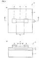
- FIG. 1A and 1B are schematic views illustrating an example of a semiconductor device according to one embodiment of the present invention, in which FIG. 1A is a schematic plan view, and FIG. 1B is a schematic cross-sectional view taken along line IB-IB illustrated in FIG. It is a schematic sectional drawing which shows an example of the manufacturing method of the semiconductor device which concerns on 1 aspect of this invention.
- An oxide sintered body according to an embodiment of the present invention is an oxide sintered body containing indium, tungsten, and zinc, includes a bixbite type crystal phase as a main component, and has an apparent appearance.
- the density is larger than 6.5 g / cm 3 and not larger than 7.1 g / cm 3 . Since the oxide sintered body of the present embodiment contains a bixbite type crystal phase as a main component and an apparent density is larger than 6.5 g / cm 3 and not larger than 7.1 g / cm 3 , It is suitably used as a sputtering target for forming an oxide semiconductor film by a sputtering method.
- the content of tungsten with respect to the total of indium, tungsten and zinc in the oxide sintered body is greater than 1.2 atomic% and smaller than 30 atomic%.
- the zinc content relative to the sum of indium, tungsten and zinc is greater than 1.2 atom% and less than 30 atom%.
- the bixbite type crystal phase includes indium oxide as a main component, and includes tungsten and zinc that are dissolved in at least a part of the bixbite type crystal phase. be able to.
- the ratio of the ON current to the OFF current can be increased with a low driving voltage.
- the oxide sintered body of the present embodiment contains at least one element selected from the group consisting of aluminum, titanium, chromium, gallium, hafnium, zirconium, silicon, molybdenum, vanadium, niobium, tantalum, and bismuth. Further can be included.
- the content of the element with respect to the total of indium, tungsten, zinc and the element in the oxide sintered body can be 0.1 atomic% or more and 10 atomic% or less.
- the oxide sintered body of the present embodiment contains the above elements, the atomic ratio of silicon to indium (atomic ratio) in the oxide sintered body is a value smaller than 0.007. Can do. Thereby, the electrical resistivity of the oxide semiconductor film formed using the sputtering target containing this oxide sintered compact can be raised.
- the atomic ratio (atomic ratio) of titanium to indium in the oxide sintered body is a value smaller than 0.004. Can do. Thereby, the electrical resistivity of the oxide semiconductor film formed using the sputtering target containing this oxide sintered compact can be raised.
- the oxide sintered body of the present embodiment can include tungsten having at least one valence of hexavalence and tetravalence.
- the oxide sintered body of the present embodiment can include tungsten having a bond energy measured by X-ray photoelectron spectroscopy of 245 eV or more and 250 eV or less.
- a sputter target according to another embodiment of the present invention includes the oxide sintered body of the above embodiment. Since the sputter target of this embodiment includes the oxide sintered body of the above-described embodiment, it is suitably used for forming an oxide semiconductor film of a semiconductor device having high characteristics by a sputtering method.
- a semiconductor device includes an oxide semiconductor film formed by sputtering using the sputtering target of the above embodiment. Since the semiconductor device of this embodiment includes an oxide semiconductor film formed by a sputtering method using the sputtering target of the above embodiment, high characteristics can be exhibited.
- the semiconductor device described here is not particularly limited, but a TFT (thin film transistor) including an oxide semiconductor film formed by a sputtering method using the sputtering target of the above embodiment as a channel layer is a preferable example.
- the content of tungsten with respect to the total of indium, tungsten, and zinc in the oxide semiconductor film is set to be larger than 1.2 atomic% and smaller than 30 atomic%.
- the zinc content relative to the sum of indium, tungsten and zinc can be greater than 1.2 atomic percent and less than 30 atomic percent. Accordingly, in a semiconductor device including an oxide semiconductor film as a channel layer, the ratio of the ON current to the OFF current can be increased with a low driving voltage.
- the atomic ratio of tungsten to zinc in the oxide semiconductor film can be made larger than 0.5 and smaller than 3.0. Accordingly, in a semiconductor device including an oxide semiconductor film as a channel layer, the ratio of the ON current to the OFF current can be increased with a low driving voltage.
- the atomic ratio of silicon to indium in the oxide semiconductor film can be less than 0.007. Accordingly, the electrical resistivity of the oxide semiconductor film can be increased to 1 ⁇ 10 2 ⁇ cm or more.
- the atomic ratio of titanium to indium in the oxide semiconductor film can be less than 0.004. Accordingly, the electrical resistivity of the oxide semiconductor film can be increased to 1 ⁇ 10 2 ⁇ cm or more.
- the oxide semiconductor film may include tungsten having at least one valence of hexavalence and tetravalence. Accordingly, in a semiconductor device including an oxide semiconductor film as a channel layer, the ratio of the ON current to the OFF current can be increased with a low driving voltage.
- the oxide semiconductor film may contain tungsten having a binding energy measured by X-ray photoelectron spectroscopy of 245 eV or more and 250 eV or less. Accordingly, in a semiconductor device including an oxide semiconductor film as a channel layer, the ratio of the ON current to the OFF current can be increased with a low driving voltage.
- a method for manufacturing an oxide sintered body according to still another embodiment of the present invention is a method for manufacturing an oxide sintered body according to the above-described embodiment, and includes a zinc oxide powder and a tungsten oxide powder.
- a step of preparing a primary mixture, a step of forming a calcined powder by heat-treating the primary mixture, a step of preparing a secondary mixture of raw material powders including the calcined powder, and forming the secondary mixture The step of forming a sintered body and the step of forming an oxide sintered body by sintering the molded body, the step of forming the calcined powder is performed at 550 ° C. or higher and 1200 ° C. in an oxygen-containing atmosphere.
- the oxide oxide sintered body has a higher apparent density and can be suitably used as a sputtering target. A knot is obtained.
- the tungsten oxide powder is at least one crystal phase selected from the group consisting of a WO 3 crystal phase, a WO 2 crystal phase, and a WO 2.72 crystal phase. Can be included. Thereby, the apparent density of the oxide sintered body is increased, and an oxide sintered body that can be suitably used as a sputtering target is obtained.
- the tungsten oxide powder may have a median particle diameter d50 of 0.1 ⁇ m or more and 4 ⁇ m or less. Thereby, the apparent density of the oxide sintered body is increased, and an oxide sintered body that can be suitably used as a sputtering target is obtained.
- the double oxide may contain a ZnWO 4 type crystal phase. Thereby, the apparent density of the oxide sintered body is increased, and an oxide sintered body that can be suitably used as a sputtering target is obtained.
- the oxide sintered body of the present embodiment is an oxide sintered body containing indium, tungsten, and zinc, includes a bixbyite crystal phase as a main component, and has an apparent density of 6.5 g / cm. It is larger than 3 and 7.1 g / cm 3 or less. Since the oxide sintered body of the present embodiment contains a bixbite type crystal phase as a main component and an apparent density is larger than 6.5 g / cm 3 and not larger than 7.1 g / cm 3 , It is suitably used as a sputtering target for forming an oxide semiconductor film by a sputtering method.
- the “bixbite type crystal phase” means a bixbite crystal phase and a phase having the same crystal structure as the bixbite crystal phase, and at least a part of the bixbite crystal phase is indium (In).
- the bixbite crystal phase is one of the crystal phases of indium oxide (In 2 O 3 ), refers to the crystal structure defined in JCPDS card 6-0416, and is a rare earth oxide C-type phase (or C-rare). Also called soil structure phase.
- the bixbite type crystal layer can be identified by X-ray diffraction. That is, the existence of a bixbite type crystal phase is confirmed by X-ray diffraction, and the spacing between each plane can be measured.
- “comprising a bixbite type crystal phase as a main component” means that the proportion of the bixbite type crystal phase in the oxide sintered body (the bixbite type crystal phase occupancy rate described later) is 90% or more. Means.
- the oxide sintered body may contain other crystal phases such as a crystal phase that is unavoidably mixed. A method for discriminating between the bixbite type crystal phase and the other crystal phases is as follows.
- the phase confirmed by X-ray diffraction may be only a bixbite type crystal phase.
- the bixbite type crystal phase is the main component.
- X-ray diffraction confirms the presence of a bixbite type crystal phase and the presence of other crystal phases
- a sample is taken from a portion of the oxide sintered body, and the surface of the sample is polished and smoothed. To. Subsequently, the surface of the sample was observed with SEM (scanning secondary electron microscope) using SEM-EDX (scanning secondary electron microscope with an energy dispersive fluorescent X-ray analyzer), and each crystal particle was observed.
- the metal elemental composition ratio is analyzed by EDX (energy dispersive fluorescence X-ray analyzer).
- the crystal particles are grouped according to the tendency of the composition ratio of the metal elements of the crystal particles.
- a group of crystal grains having a high Zn content, a high W content, or both, and a group of crystal grains having a very low Zn content and W content and a high In content Can be divided into A group of crystal grains having a high Zn content, a high W content, or both are other crystal phases, and a group of crystal grains having a very low Zn content and a low W content and a high In content. Concludes that it is an In 2 O 3 type phase that is a bixbite type crystal phase.
- the occupancy rate of the bixbite type crystal phase in the oxide sintered body is defined as the ratio (percentage) of the area of the bixbite type crystal phase to the measurement surface of the oxide sinter. Therefore, the oxide sintered body of the present embodiment has a bixbite type crystal phase as a main component, and the bixbite type crystal phase occupancy defined above is 90% or more.
- the oxide sintered body of the present embodiment has an apparent density greater than 6.5 g / cm 3 and 7.1 g / cm 3 or less.
- the oxide sintered body disclosed in JP-A-2006-347807 has an apparent density of 4.0 g / cm 3 or more and 6.5 g / cm 3 or less, and the oxide of this embodiment. The apparent density of the sintered body is lower than that of the sintered body.
- the theoretical density of the bixbite type crystal phase that is the main component of the oxide sintered body of the present embodiment is that the theoretical density of the bixbite crystal phase formed of indium oxide is 7.28 g / cm 3 , and In consideration of the substitutional solid solution of tungsten and zinc at a ratio of 1.2 atomic% to 30 atomic% in at least a part of the bixbite crystal phase, the minimum is 7.19 g / cm 3 and the maximum Is considered to be 7.24 g / cm 3 . Then, the percentage of the apparent density of the sintered body relative to the theoretical density, that is, the relative density of the sintered body is 55.2% or more and 90.4% of the oxide sintered body disclosed in JP-A-2006-347807. On the other hand, the oxide sintered body of the present embodiment is extremely high, being higher than 90.4% and not higher than 99.0%.
- the apparent density of the sintered body is preferably as high as possible.
- the low apparent density of the sintered body means that there are many voids in the sintered body.
- the sputter target is used while its surface is etched with argon ions during use. Therefore, if there are vacancies in the sintered body, this is exposed during film formation and the internal gas is released, so that the gas released from the target is mixed in the deposited oxide semiconductor thin film, Film characteristics deteriorate.
- the oxide sintered body of the present embodiment has an apparent density greater than 6.5 g / cm 3 . Since it is as large as 1 g / cm 3 or less, it is suitably used as a sputtering target for forming an oxide semiconductor film of a semiconductor device having high characteristics by a sputtering method.
- the content of tungsten relative to the total of indium, tungsten, and zinc in the oxide sintered body is as follows. More than 1.2 atom% and less than 30 atom%, the zinc content relative to the sum of indium, tungsten and zinc in the oxide sintered body (hereinafter also referred to as “Zn content” of the oxide sintered body) Is greater than 1.2 atomic percent and smaller than 30 atomic percent.
- a semiconductor device for example, TFT
- the ratio of the ON current to the OFF current can be increased with a low driving voltage. Can do.
- the W content of the oxide sintered body is preferably larger than 2.0 atomic% and lower than 15 atomic%, more preferably larger than 4.0 atomic% and smaller than 12 atomic%.
- the Zn content of the oxide sintered body is preferably larger than 2.0 atomic% and lower than 15 atomic%, more preferably larger than 4.0 atomic% and smaller than 12 atomic%. .
- the W content of the oxide sintered body is 1.2 atomic% or less
- a semiconductor device for example, TFT
- TFT semiconductor film formed using the oxide sintered body as a channel layer
- the OFF current increases, and the ratio of the ON current to the OFF current becomes small.
- the W content of the oxide sintered body is 30 atomic% or more
- the semiconductor device including the oxide semiconductor film formed using the oxide sintered body as a channel layer the ON current is reduced, Or, at a low driving voltage, the ratio of the ON current to the OFF current becomes small.
- the OFF current increases. As a result, the ratio of the ON current to the OFF current becomes small.
- the Zn content of the oxide sintered body is 30 atomic% or more, in a semiconductor device including an oxide semiconductor film formed using the oxide sintered body as a channel layer, the ON current is reduced, Or, at a low driving voltage, the ratio of the ON current to the OFF current becomes small.
- the bixbite type crystal phase preferably contains indium oxide as a main component and includes tungsten and zinc that are solid-solved in at least a part of the bixbite type crystal phase.
- a semiconductor device for example, TFT
- the ratio of the ON current to the OFF current can be increased with a low driving voltage. Can do.
- the bixbite type crystal phase contains indium oxide as a main component and tungsten and zinc are dissolved in at least a part thereof” means the bixbite crystal phase.
- Form in which tungsten and zinc are solid-dissolved in substitutional form in at least part of the crystal lattice of indium oxide, or form in which interstitial solid-solution is formed between crystal lattices, or substitutional type and interstitial type Means a form that is solid-solved in both forms.
- the distance between the planes defined in JCPDS card 6-0416 may be larger, It becomes narrower.
- the peak position shifts to the high angle side or shifts to the low angle side. This peak shift is confirmed, and SEM-EDX (scanning secondary electron microscope with an energy dispersive fluorescent X-ray analyzer) and TEM-EDX (transmission with an energy dispersive fluorescent X-ray analyzer) are used.
- SEM-EDX scanning secondary electron microscope with an energy dispersive fluorescent X-ray analyzer
- TEM-EDX transmission with an energy dispersive fluorescent X-ray analyzer
- existing elements are identified using ICP (inductively coupled plasma) mass spectrometry, SEM-EDX, and other element identification methods, and the presence of zinc and tungsten along with indium has been confirmed. Then, it can be determined that tungsten or zinc is dissolved in the bixbite type crystal phase by confirming that no oxide of zinc, oxide of tungsten, or double oxide of zinc and tungsten is confirmed.
- ICP inductively coupled plasma
- the oxide sintered body of the present embodiment includes aluminum (Al), titanium (Ti), chromium (Cr), gallium (Ga), hafnium (Hf), zirconium (Zr), silicon (Si), and molybdenum (Mo). And at least one element M selected from the group consisting of vanadium (V), niobium (Nb), tantalum (Ta), and bismuth (Bi).
- the content of element M with respect to the sum of indium (In), tungsten (W), zinc (Zn) and element (M) in the oxide sintered body (hereinafter referred to as “M content of oxide sintered body” Is preferably 0.1 atomic percent or more and 10 atomic percent or less.
- the ratio of the ON current to the OFF current can be increased with a low driving voltage.
- the M content of the oxide sintered body is more preferably from 0.1 atomic% to 5 atomic%, and further preferably from 0.1 atomic% to 1 atomic%.
- the oxide sintered body when the content of at least one additive element of Al, Ti, Cr, Ga, Hf, Si, V, and Nb is 0.1 atomic% or more, the oxide sintered body is used. Although there is an effect that the OFF current of a semiconductor device including an oxide semiconductor is reduced, when the content of the additive element is larger than 10 atomic%, the ON current of the semiconductor device tends to be reduced.
- the content of at least one additive element of Zr, Mo, Ta, and Bi is 0.1 atomic% or more, ON of a semiconductor device including an oxide semiconductor obtained using the oxide sintered body
- the content of the additive element is larger than 10 atomic%, the OFF current of the semiconductor device tends to increase.
- the oxide semiconductor film formed using the oxide sintered body according to the present embodiment is used as a semiconductor layer of a semiconductor device, it is desirable that the electrical resistivity is higher than that desired for a transparent conductive film.
- the oxide semiconductor film formed using the oxide sintered body according to this embodiment preferably has an electric resistivity of 1 ⁇ 10 2 ⁇ cm or more.
- the Si content that can be contained in the oxide sintered body is preferably less than 0.007 in terms of the Si / In atomic ratio
- the Ti content that can be contained in the oxide sintered body Is preferably smaller than 0.004 in Ti / In atomic ratio.
- the electrical resistivity of the oxide semiconductor film is measured by a four-terminal method.
- Mo electrode is formed by sputtering method as electrode material, voltage between -40V to + 40V is swept between outer electrodes, current is passed, voltage between inner electrodes is measured, and electric resistivity is calculated To do.
- the oxide sintered body of the present embodiment preferably contains tungsten having at least one valence of hexavalent and tetravalent. According to such an oxide sintered body, in a semiconductor device (for example, TFT) including an oxide semiconductor film formed using the oxide sintered body as a channel layer, the ratio of the ON current to the OFF current can be increased with a low driving voltage. Can do.
- a semiconductor device for example, TFT
- the oxide sintered body of the present embodiment preferably also contains tungsten having a bond energy measured by X-ray photoelectron spectroscopy of 245 eV or more and 250 eV or less.
- tungsten having a bond energy measured by X-ray photoelectron spectroscopy of 245 eV or more and 250 eV or less.
- a semiconductor device for example, TFT
- the ratio of the ON current to the OFF current can be increased with a low driving voltage. Can do.
- Tungsten is known to have various valences as ions.
- a semiconductor device for example, TFT
- TFT including, as a channel layer, an oxide semiconductor film formed using such an oxide sintered body when having at least one valence of tetravalence and hexavalence
- the ON current can be increased and the ratio of the ON current to the OFF current can be increased with a low drive voltage.
- the valence of tungsten may be only tetravalent or only hexavalent, may include both tetravalent and hexavalent, or may include other valences that are not the main component.
- Tungsten having at least one valence of tetravalent and hexavalent is preferably 70 atomic% or more of the total amount of tungsten.
- the valence can be obtained from the bond energy of tungsten, and the valence valence ratio can be obtained by peak separation.
- the semiconductor device includes an oxide semiconductor film as a channel layer when the peak position is 245 eV or more and 250 eV or less.
- the ON current can be increased, and the ratio of the ON current to the OFF current can be increased with a low driving voltage.
- the binding energy is more preferably 246 eV or more and 249 eV or less, and further preferably 246 eV or more and 248 eV or less.
- the oxide sintered body of the present embodiment is mainly hexavalent, and a semiconductor device (for example, a TFT) including an oxide semiconductor film formed using the oxide sintered body as a channel layer. ) Is preferable from the viewpoint of increasing the ON current and increasing the ratio of the ON current to the OFF current at a low driving voltage.
- the method for producing an oxide sintered body according to the present embodiment is a method for producing an oxide sintered body according to Embodiment 1, in which a primary mixture of zinc oxide powder and tungsten oxide powder is prepared.
- a step of forming a calcined powder by heat-treating the primary mixture a step of preparing a secondary mixture of raw material powders including the calcined powder, a step of forming a molded body by molding the secondary mixture, Forming an oxide sintered body by sintering the formed body.
- the primary mixture is heat-treated at a temperature of 550 ° C. or higher and lower than 1200 ° C. in an oxygen-containing atmosphere, thereby forming a double oxide powder containing zinc and tungsten as the calcined powder. Including that.
- the primary mixture of zinc oxide powder and tungsten oxide powder is 550 ° C. or higher and 1200 ° C. in an oxygen-containing atmosphere. Since it includes forming a double oxide powder containing zinc and tungsten as the calcined powder by heat treatment at a temperature lower than 0 ° C., the apparent density of the oxide sintered body is increased and it is suitably used as a sputtering target. An oxide sintered body that can be obtained is obtained.
- a primary mixture is prepared by mixing zinc oxide powder and tungsten oxide powder in a raw material powder, and the primary mixture is brought into an atmosphere containing oxygen.
- the apparent density of the oxide sintered body can be increased by performing heat treatment at a temperature of 550 ° C. or more and less than 1200 ° C. to form a double oxide powder containing zinc and tungsten as the calcined powder.
- the double oxide may be deficient in oxygen or substituted with metal.
- the heat treatment temperature is less than 550 ° C., a double oxide powder containing zinc and tungsten is not obtained, and when it is 1200 ° C. or higher, the double oxide powder containing zinc and tungsten is decomposed or scattered, The particle size of the powder becomes too large.
- a primary mixture of zinc oxide powder and tungsten oxide powder is heat-treated at a temperature of 550 ° C. or more and less than 1200 ° C. in an atmosphere containing oxygen, and a double oxide containing zinc and tungsten as a calcined powder
- tungsten in the oxide sintered body can contain at least one valence of tetravalent and hexavalent.
- the ratio of the ON current to the OFF current can be increased with a low driving voltage in a semiconductor device including, as a channel layer, an oxide semiconductor film formed using a sputtering target including the obtained oxide sintered body. .
- the double oxide containing zinc and tungsten contains a ZnWO 4 type crystal phase to increase the apparent density of the oxide sintered body, and the hexavalent and tetravalent in the oxide sintered body. From the viewpoint of increasing the proportion of tungsten having at least one valence, it is preferable.
- the ZnWO 4 type crystal phase is a zinc tungstate compound crystal phase having a crystal structure represented by the space group P12 / c1 (13) and having a crystal structure defined by JCPDS card 01-088-0251. . As long as these crystal systems are shown, oxygen may be deficient or metal may be dissolved, and the lattice constant may be changed.
- the tungsten oxide powder contains at least one crystal phase selected from the group consisting of the WO 3 crystal phase, the WO 2 crystal phase, and the WO 2.72 crystal phase, thereby increasing the apparent density of the oxide sintered body. From the viewpoint of increasing the proportion of tungsten having at least one valence of hexavalent and tetravalent in the oxide sintered body. From this point of view, the tungsten oxide powder is more preferably at least one powder selected from the group consisting of WO 3 powder, WO 2 powder, and WO 2.72 powder.
- the median particle diameter d50 of the tungsten oxide powder is preferably 0.1 ⁇ m or more and 4 ⁇ m or less, more preferably 0.2 ⁇ m or more and 2 ⁇ m or less, and more preferably 0.3 ⁇ m or more from the viewpoint of increasing the apparent density of the oxide sintered body. More preferably, it is 1.5 ⁇ m or less.
- the median particle diameter d50 is a value obtained by BET specific surface area measurement. When the median particle size d50 is smaller than 0.1 ⁇ m, it is difficult to handle the powder, and it is difficult to uniformly mix the zinc oxide powder and the tungsten oxide powder.
- the median particle size d50 is larger than 4 ⁇ m, the mixed oxide powder containing zinc and tungsten obtained by heat treatment at a temperature of 550 ° C. or more and less than 1200 ° C. in an atmosphere containing oxygen after mixing with the zinc oxide powder.
- the particle size also increases, and it is difficult to increase the apparent density of the oxide sintered body.
- the double oxide preferably contains a ZnWO 4 type crystal phase from the viewpoint of increasing the apparent density of the oxide sintered body.
- the manufacturing method of the oxide sintered body of the present embodiment is not particularly limited, but includes the following steps from the viewpoint of efficiently forming the oxide sintered body of Embodiment 1.
- tungsten oxide powder for example, WO 3 powder, WO 2.72 powder, WO 2 powder
- ZnO powder a material powder constituting an oxide sintered body such as a material powder
- the tungsten oxide powder not only the WO 3 powder but also a powder having a chemical composition deficient in oxygen as compared with the WO 3 powder such as the WO 2.72 powder and the WO 2 powder may be used as a raw material. This is preferable from the viewpoint of setting the valence of tungsten in the sintered body to at least one of hexavalent and tetravalent.
- the purity of the raw material powder is preferably a high purity of 99.9% by mass or more from the viewpoint of preventing unintended mixing of metal elements and Si into the oxide sintered body and obtaining stable physical properties.
- the median particle diameter d50 of the tungsten oxide powder is preferably 0.1 ⁇ m or more and 4 ⁇ m or less from the viewpoint of increasing the apparent density of the oxide sintered body.
- tungsten oxide powder (WO 3 powder, WO 2.72 powder and / or WO 2 powder) and zinc oxide powder (ZnO powder) are pulverized and mixed To do.
- a tungsten oxide powder and a zinc oxide powder are used as a raw material powder in a molar ratio of 1: 1, and Zn 2 W 3
- tungsten oxide powder and zinc oxide powder are mixed as a raw material powder in a molar ratio of 3: 2.
- the use of the ZnWO 4 type phase is preferable from the viewpoint of increasing the apparent density of the oxide sintered body.
- the method for pulverizing and mixing the raw material powder is not particularly limited and may be any of dry and wet methods. Specifically, the raw material powder is pulverized and mixed using a ball mill, a planetary ball mill, a bead mill, or the like. In this way, a primary mixture of raw material powders is obtained.
- a drying method such as natural drying or a spray dryer may be preferably used for drying the mixture obtained using the wet pulverization and mixing method.
- the calcining temperature of the primary mixture is preferably less than 1200 ° C. so that the particle size of the calcined product becomes too large and the apparent density of the sintered body does not decrease.
- the temperature is preferably 550 ° C. or higher. More preferably, it is 550 degreeC or more and less than 1000 degreeC, More preferably, it is 550 degreeC or more and 800 degrees C or less.
- the calcining atmosphere may be an atmosphere containing oxygen, but is preferably an atmospheric atmosphere pressurized to atmospheric pressure or air, or an oxygen-nitrogen mixed atmosphere containing 25% by volume or more of oxygen. Further, since the productivity is high, an atmospheric pressure-air atmosphere is more preferable.
- Step of preparing secondary mixture of raw material powder including calcined powder Next, the obtained calcined powder and the In 2 O 3 powder of the raw material powder are mixed by the same pulverization method as described above, Grind and mix. In this way, a secondary mixture of raw material powders is obtained.
- Step of forming a molded body by molding the secondary mixture the obtained secondary mixture is molded.
- the method for forming the secondary mixture is not particularly limited, but from the viewpoint of increasing the apparent density of the sintered body, a uniaxial press method, a CIP (cold isostatic treatment) method, a casting method and the like are preferable. In this way, a molded body is obtained.
- Step of forming an oxide sintered body by sintering the molded body the obtained molded body is sintered. It is preferable not to use a hot press sintering method.
- the sintering temperature of the molded body is not particularly limited, but is preferably 900 ° C. or higher and 1200 ° C. or lower from the viewpoint that the apparent density of the oxide sintered body to be formed is larger than 6.5 g / cm 3 .
- the sintering atmosphere is not particularly limited, but an atmospheric pressure-atmosphere atmosphere is preferable from the viewpoint of preventing the generation of cracks by preventing the grain size of the constituent crystals of the oxide sintered body from increasing. In this way, the oxide sintered body of the present embodiment is obtained.
- the sputter target of the present embodiment includes the oxide sintered body of the first embodiment. Since the sputter target of this embodiment includes the oxide sintered body of Embodiment 1, it can be suitably used for forming an oxide semiconductor film of a semiconductor device with high characteristics by a sputtering method.
- the sputter target of the present embodiment preferably includes the oxide sintered body of the first embodiment in order to be suitably used for forming an oxide semiconductor film of a semiconductor device having high characteristics by a sputtering method. More preferably, the oxide sintered body of Embodiment 1 is used.
- a semiconductor device 10 of this embodiment includes an oxide semiconductor film 14 formed by a sputtering method using the oxide sintered body of Embodiment 1 as a sputtering target. Since the semiconductor device of this embodiment includes an oxide semiconductor film formed by a sputtering method using the oxide sintered body of Embodiment 1 as a sputtering target, the semiconductor device has high characteristics.
- the semiconductor device 10 of the present embodiment is not particularly limited.
- the semiconductor device 10 includes, as a channel layer, the oxide semiconductor film 14 formed by a sputtering method using the oxide sintered body of Embodiment 1 as a sputtering target. It is a certain TFT (Thin Film Transistor).
- a TFT which is an example of the semiconductor device 10 of this embodiment includes an oxide semiconductor film 14 formed by sputtering using the oxide sintered body of the above embodiment as a target, and thus has a low OFF current. At the same time, the ratio of the ON current to the OFF current becomes high at a low driving voltage.
- the TFT which is the semiconductor device 10 of the present embodiment is arranged as a substrate 11, a gate electrode 12 arranged on the substrate 11, and an insulating layer on the gate electrode 12, as shown in FIG.
- the content of tungsten with respect to the total of indium, tungsten, and zinc in the oxide semiconductor film 14 (hereinafter, from the viewpoint of increasing the ratio of the ON current to the OFF current at a low driving voltage) , which is also referred to as “W content” of the oxide semiconductor film 14) and larger than 1.2 atomic% and smaller than 30 atomic%, and the zinc content relative to the total of indium, tungsten, and zinc in the oxide semiconductor film 14.
- Zn content is preferably greater than 1.2 atomic% and smaller than 30 atomic%.
- the chemical composition of the oxide semiconductor film 14, that is, the content of various elements, is measured by RBS (Rutherford backscattering analysis).
- the W content of the oxide semiconductor film 14 is more preferably greater than 2.0 atomic percent and smaller than 15 atomic percent, and more preferably greater than 4.0 atomic percent and smaller than 12 atomic percent.
- the Zn content of the oxide semiconductor film 14 is more preferably larger than 2.0 atomic% and smaller than 15 atomic%, and more preferably larger than 4.0 atomic% and smaller than 12 atomic%. preferable.
- the OFF current increases, and the OFF current is reduced.
- the ON current ratio tends to be small.
- the W content of the oxide semiconductor film 14 is 30 atomic% or more, in the TFT which is the semiconductor device 10 including the oxide semiconductor film 14 as a channel layer, the ON current is reduced or at a low driving voltage. The ratio of the ON current to the OFF current tends to be small.
- the OFF current increases, and the OFF current
- the ON current ratio tends to be small.
- the ON current is reduced or at a low driving voltage. The ratio of the ON current to the OFF current tends to be small.
- the atomic ratio of tungsten to zinc contained in the oxide semiconductor film 14 (hereinafter referred to as “W / Zn”) from the viewpoint of increasing the ratio of the ON current to the OFF current at a low driving voltage.
- W / Zn the atomic ratio of tungsten to zinc contained in the oxide semiconductor film 14
- the chemical composition of the oxide semiconductor film 14, that is, the W / Zn atomic ratio is measured by RBS (Rutherford backscattering analysis).
- the W / Zn atomic ratio is 3.0 or more
- the OFF current increases, and the ratio of the ON current to the OFF current decreases. End up.
- the W / Zn atomic ratio is 0.5 or less
- the ON current decreases, or the ON current with respect to the OFF current is reduced at a low driving voltage. The current ratio becomes small.
- the oxide semiconductor film 14 is at least hexavalent and tetravalent. It is preferable to include tungsten having one valence.
- the oxide semiconductor film 14 has a binding energy measured by X-ray photoelectron spectroscopy of 245 eV or more from the viewpoint of increasing the ratio of the ON current to the OFF current at a low driving voltage. It is preferable to contain tungsten of 250 eV or less.
- the manufacturing method of the semiconductor device 10 of the present embodiment is not particularly limited, but the step of forming the gate electrode 12 on the substrate 11 from the viewpoint of efficiently manufacturing the high-performance semiconductor device 10.
- FIG. 2A a step of forming a gate insulating film 13 as an insulating layer over the gate electrode 12
- an oxide semiconductor film 14 as a channel layer over the gate insulating film 13.
- FIG. 2C a step of forming the source electrode 15 and the drain electrode 16 over the oxide semiconductor film 14 so as not to contact each other
- gate electrode 12 is formed on substrate 11. Although there is no restriction
- the gate electrode 12 is not particularly limited, but a Mo electrode, a Ti electrode, a W electrode, an Al electrode, a Cu electrode, or the like is preferable because it has high oxidation resistance and low electrical resistance.
- the method for forming the gate electrode 12 is not particularly limited, but a vacuum vapor deposition method, a sputtering method, or the like is preferable because it can be uniformly formed in a large area on the main surface of the substrate.
- a gate insulating film 13 is formed on the gate electrode 12 as an insulating layer.
- the gate insulating film 13 is not particularly limited, but an SiO x film, an SiN y film, or the like is preferable from the viewpoint of high insulation.
- the method for forming the gate insulating film 13 is not particularly limited. However, plasma CVD (chemical vapor deposition) is preferable because it can be uniformly formed in a large area on the main surface of the substrate 11 on which the gate electrode is formed and the insulating property is ensured.
- the phase deposition method is preferred.
- an oxide semiconductor film 14 is formed over the gate insulating film 13 as a channel layer.
- the oxide semiconductor film 14 is formed by sputtering using the oxide sintered body of Embodiment 1 as a sputtering target from the viewpoint of manufacturing the semiconductor device 10 having high characteristics.
- sputtering means that a target and a substrate are arranged facing each other in a deposition chamber, a voltage is applied to the target, and the surface of the target is sputtered with rare gas ions, thereby forming the target from the target.
- This is a method of forming a film composed of atoms constituting a target by discharging atoms to be deposited on a substrate (including the substrate on which the gate electrode and the gate insulating film are formed).
- Source electrode 15 and drain electrode 16 are formed on oxide semiconductor film 14 so as not to contact each other.
- the source electrode 15 and the drain electrode 16 are not particularly limited, but have a high oxidation resistance, a low electric resistance, and a low contact electric resistance with the oxide semiconductor film 14, so that the Mo electrode, the Ti electrode, and the W electrode Al electrodes, Cu electrodes and the like are preferable.
- a method for forming the source electrode 15 and the drain electrode 16 is not particularly limited. However, the source electrode 15 and the drain electrode 16 can be uniformly formed in a large area on the main surface of the substrate 11 on which the oxide semiconductor film 14 is formed. The method is preferred.
- a method for forming the source electrode 15 and the drain electrode 16 so as not to contact each other is not particularly limited, but the source electrode 15 and the drain having a large area and a uniform area on the main surface of the substrate 11 on which the oxide semiconductor film 14 is formed. From the viewpoint that the pattern of the electrode 16 can be formed, formation by an etching method using a photoresist is preferable.
- the valence of tungsten contained in the oxide semiconductor film in the oxide sintered body of Embodiment 1, the sputter target of Embodiment 3, and the semiconductor device of Embodiment 4 is measured by X-ray photoelectron spectroscopy (XPS).
- XPS X-ray photoelectron spectroscopy
- the ratio of tungsten having at least one valence of hexavalent and tetravalent can be determined from the intensity areas of the peaks existing in these ranges and the peaks existing in other ranges.
- the total peak intensity area ratio of hexavalent and tetravalent to the total peak intensity area of tungsten is 70% or more, it can be determined that tungsten having at least one valence of hexavalent and tetravalent is the main component. .
- the oxide semiconductor film in which tungsten contained in the oxide semiconductor film 14 in the oxide sintered body of Embodiment 1, the sputter target of Embodiment 3, and the semiconductor device 10 of Embodiment 4 is mainly hexavalent.
- the TFT thin film transistor
- the fact that the valence of tungsten is hexavalent can be confirmed from the fact that the binding energy of tungsten investigated by X-ray photoelectron spectroscopy is 245 eV or more and 250 eV or less.
- Example 1 to Example 8 Preparation of Powder Raw Material Tungsten oxide powder (shown as “W” in Table 1) having the type and median particle size d50 shown in Table 1 and a purity of 99.99% by mass, and median particle size d50 of 1.
- ZnO powder having a purity of 99.99% by mass at 0 ⁇ m (indicated as “Z” in Table 1) and In 2 O 3 powder having a median particle diameter d50 of 1.0 ⁇ m and a purity of 99.99% by mass
- Table 1 was written as “I” in FIG.
- a primary mixture of raw material powder was prepared by putting a tungsten oxide powder and a ZnO powder among the prepared raw material powders in a ball mill and pulverizing and mixing for 18 hours.
- Ethanol was used as a dispersion medium during the above pulverization and mixing.
- the obtained primary mixture of raw material powders was dried in the air.
- the obtained primary mixture of raw material powder was put in an alumina crucible and calcined at a temperature of 650 ° C. for 8 hours in an air atmosphere.
- the calcination temperature is preferably lower from the viewpoint that the grain size of the calcined powder can be made as small as possible as long as the crystal phase is formed. In this way, a calcined powder containing a ZnWO 4 type phase as a crystal phase was obtained.
- the crystal phase of the obtained oxide sintered body was identified by taking a sample from a part of the oxide sintered body and analyzing the crystal by a powder X-ray diffraction method. Cu X-rays were used as X-rays. Table 1 summarizes the crystal phases present in the oxide sintered body.
- the In 2 O 3 type phase which is a bixbite type crystal phase
- the main component the In 2 O 3 type phase, which is a bixbite type crystal phase.
- the existence of a bixbite type crystal phase and the presence of other crystal phases were confirmed by X-ray diffraction.
- the phase confirmed by X-ray diffraction was only a bixbite type crystal phase.
- the bixbite type crystal phase was the main component.
- a sample was taken from a part of the oxide sintered body, and the surface of the sample was polished and smoothed. Subsequently, the surface of the sample was observed with SEM using SEM-EDX, and the composition ratio of the metal elements of each crystal particle was analyzed with EDX.
- the crystal particles were grouped according to the tendency of the composition ratio of the metal elements of the crystal particles, a group of crystal particles having a high Zn content and a high W content, a Zn content and a W content being very low, It could be divided into a group of crystal grains with high content.
- the group of crystal grains having a high Zn content and W content is a crystal phase other than the bixbite type crystal phase, and the group of crystal grains having a very low Zn content and W content and a high In content is a bixbite type. It was concluded that the crystal phase was an In 2 O 3 type crystal phase.
- the bixbite type crystal phase When the ratio of the area of the In 2 O 3 type crystal phase that is the bixbite type crystal phase to the measurement surface of the oxide sintered body (bixbite type crystal phase occupancy) is 90% or more, the bixbite type crystal phase
- the In 2 O 3 type crystal phase was determined as the main component.
- Each of the oxide sintered bodies of Examples 1 to 8 was mainly composed of an In 2 O 3 type crystal phase which is a bixbite type crystal phase.
- the apparent density of the obtained oxide sintered body was determined by the Archimedes method.
- X-ray photoelectron spectroscopy (XPS) was used as a method for measuring the valence of tungsten contained in the obtained oxide sintered body and sputtering target.
- the peak of the binding energy of tungsten 4d5 / 2 of WO 3 where tungsten is hexavalent appears in the range of 247 eV or more and 249 eV or less, and the peak of binding energy of tungsten 4d5 / 2 of WO 2 where tungsten metal and tungsten are tetravalent is It appears in the range of 243 eV to 244 eV.
- Table 2 summarizes the valence of tungsten (identified as “W valence” in Table 2) and the peak position of bond energy (denoted as “W bond energy” in Table 2) identified from XPS.
- Target The obtained oxide sintered body was processed into a target having a diameter of 3 inches (76.2 mm) and a thickness of 5.0 mm.
- a synthetic quartz glass substrate having a size of 50 mm ⁇ 50 mm ⁇ thickness 0.6 mm is prepared as a substrate 11 and sputtered on the substrate 11.
- a Mo electrode having a thickness of 100 nm was formed as the gate electrode 12 by the method.
- an amorphous SiO x film having a thickness of 200 nm was formed as a gate insulating film 13 on the gate electrode 12 by plasma CVD.
- Oxide Semiconductor Film Referring to FIG. 2C, next, a target processed from each oxide sintered body of Examples 1 to 8 is formed on the gate insulating film 13.
- An oxide semiconductor film 14 having a thickness of 35 nm was formed by the DC (direct current) magnetron sputtering method used.
- the plane of the target having a diameter of 3 inches (76.2 mm) was the sputtering surface.
- the gate insulating film 13 is exposed on the substrate 11 on which the gate electrode 12 and the gate insulating film 13 are formed on a water-cooled substrate holder in a film forming chamber of a sputtering apparatus (not shown). Arranged.
- the target was disposed at a distance of 90 mm so as to face the gate insulating film 13.
- the target was sputtered in the following manner with a vacuum of about 6 ⁇ 10 ⁇ 5 Pa in the film formation chamber.
- a mixed gas of Ar (argon) gas and O 2 (oxygen) gas was introduced into the film formation chamber up to a pressure of 0.5 Pa in a state where a shutter was put between the gate insulating film 13 and the target.
- the O 2 gas content in the mixed gas was 20% by volume.
- Sputtering discharge was caused by applying DC power of 100 W to the target, thereby cleaning the target surface (pre-sputtering) for 10 minutes.
- the oxide semiconductor film 14 was formed on the gate insulating film 13 by removing the shutter while maintaining the atmosphere in the film formation chamber. Note that no bias voltage was applied to the substrate holder, and the substrate holder was only water-cooled. At this time, the deposition time was set so that the thickness of the oxide semiconductor film 14 was 35 nm. Thus, the oxide semiconductor film 14 was formed by the DC (direct current) magnetron sputtering method using the target processed from the oxide sintered body. The oxide semiconductor film 14 functions as a channel layer in the TFT (thin film transistor) that is the semiconductor device 10.
- a source electrode forming portion 14s, a drain electrode forming portion 14d, and a channel portion 14c were formed.
- the size of the main surface of the source electrode forming portion 14s and the drain electrode forming portion 14d is 100 ⁇ m ⁇ 100 ⁇ m and the channel length C L (see FIGS. 1A and 1B and FIG. 2)
- the channel length CL refers to the distance of the channel portion 14c between the source electrode 15 and the drain electrode 16.
- the channel length C L is 20 ⁇ m
- the channel width C W (see FIGS. 1A and 1B and FIG. 2).
- the channel width C W is the width of the channel portion 14c.) was 40 ⁇ m.
- the channel portion 14c is arranged such that a thin film transistor (TFT), which is a semiconductor device, is arranged at 25 mm ⁇ 25 mm at 3 mm intervals in a 75 mm ⁇ 75 mm substrate main surface at 3 mm intervals in a 75 mm ⁇ 75 mm substrate main surface. And 25 vertical x 25 horizontal.
- TFT thin film transistor
- the substrate 11 on which the oxide semiconductor film 14 was formed in this order was immersed in the etching aqueous solution. At this time, the aqueous etching solution was heated to 45 ° C. in a hot bath.
- Source electrode 15 and drain electrode 16 were formed on oxide semiconductor film 14 separately from each other.
- a resist (not shown) is applied on the oxide semiconductor film 14 so that only the main surfaces of the source electrode forming portion 14s and the drain electrode forming portion 14d of the oxide semiconductor film 14 are exposed. Exposed and developed. On the main surfaces of the source electrode forming portion 14s and the drain electrode forming portion 14d of the oxide semiconductor film 14, the thicknesses of the Mo electrode and the drain electrode 16 having a thickness of 100 nm as the source electrode 15 are formed by sputtering. A Mo electrode having a thickness of 100 nm was formed separately from each other. Thereafter, the resist on the oxide semiconductor film 14 was peeled off.
- Such Mo electrodes as the source electrode 15 and the drain electrode 16 are arranged such that the thin film transistors (TFTs) as the semiconductor devices 10 are arranged 25 ⁇ 25 ⁇ 25 mm apart on a 75 mm ⁇ 75 mm substrate main surface at intervals of 3 mm.
- One source electrode 15 and one drain electrode 16 are arranged for one channel portion 14c.
- a TFT including the oxide semiconductor film 14 as a channel layer was manufactured as the semiconductor device 10.
- the obtained TFT as the semiconductor device 10 was heat-treated at 150 ° C. for 1 hour in a nitrogen atmosphere.
- the characteristics of the TFT as the semiconductor device 10 were evaluated as follows. First, a measuring needle was brought into contact with the gate electrode 12, the source electrode 15, and the drain electrode 16. A source-drain voltage V ds of 7 V is applied between the source electrode 15 and the drain electrode 16, and the source-gate voltage V gs applied between the source electrode 15 and the gate electrode 12 is changed from ⁇ 10V to 15V. The source-drain current I ds at that time was measured. The source-drain current I ds when the source-gate voltage V gs was ⁇ 5 V was defined as the OFF current. The values of OFF current in each example are summarized in Table 2.
- the valence of tungsten contained in the obtained oxide semiconductor film 14 was measured by X-ray photoelectron spectroscopy (XPS).
- XPS X-ray photoelectron spectroscopy
- the peak of the binding energy of tungsten 4d5 / 2 of WO 3 at which tungsten is hexavalent appears at 247 eV or more and 249 eV or less, and the peak of binding energy of tungsten 4d5 / 2 of WO 2 at which tungsten metal and tungsten are tetravalent is 243 eV. It appeared in the range of 244 eV or less.
- Table 2 summarizes the valence (expressed as “W valence” in Table 2) of tungsten identified from XPS and the peak position of the bond energy (expressed as “W bond energy” in Table 2).
- Example 9 to 12 Preparation of Powder Raw Material Tungsten oxide powder (shown as “W” in Table 1) having the type and median particle size d50 shown in Table 1 and a purity of 99.99% by mass, and median particle size d50 of 1.
- ZnO powder having a purity of 99.99% by mass at 0 ⁇ m (indicated as “Z” in Table 1) and In 2 O 3 powder having a median particle diameter d50 of 1.0 ⁇ m and a purity of 99.99% by mass (Table 1 was written as “I” in FIG.
- a primary mixture of raw material powder was prepared by putting a tungsten oxide powder and a ZnO powder among the prepared raw material powders in a ball mill and pulverizing and mixing for 18 hours.
- Ethanol was used as a dispersion medium during the above pulverization and mixing.
- the obtained primary mixture of raw material powders was dried in the air.
- TFT which is a semiconductor device
- oxide powders Al 2 O 3 , TiO 2 , Cr
- element M shown in Table 1 in addition to the calcined powder and In 2 O 3 powder are used as the raw material powder.
- an oxide sintered body containing a bixbite type crystal phase (In 2 O 3 type phase) containing tungsten and zinc as a solid solution and further containing the element M was produced.
- Table 2 shows the M content in the oxide sintered body.
- an In 2 O 3 type crystal phase which is a bixbite type crystal phase was a main component.
- the obtained oxide sintered body is processed into a target, and a TFT which is a semiconductor device including an oxide semiconductor film formed by a DC magnetron sputtering method using the target is made in the same manner as in Examples 1 to 12. Made.
- Table 1 and Table 2 summarize the physical properties of the obtained oxide sintered body and oxide semiconductor film, and the characteristics of TFT as a semiconductor device.
- the measuring methods of physical properties and characteristics are the same as in Examples 1 to 12.
- Example 1 to Example 8 or Example except that a mixture of raw material powders was prepared and then calcined and molded without sintering, when preparing the oxide sintered body.
- oxide sintered bodies were produced.
- the obtained oxide sintered body was processed into a target, and a TFT as a semiconductor device including an oxide semiconductor film formed by a DC magnetron sputtering method using the target was manufactured in the same manner as in the example. It was confirmed that there was no formation of a double oxide crystal phase by molding and sintering a mixture of raw material powders without calcining.
- the oxide sintered bodies of Comparative Examples 1 to 3 have an apparent density of 6.5 g / cm 3 or less. Between Comparative Examples 1 to 3, the molar mixing ratios of WO 2.72 powder or WO 2 powder, ZnO powder or SnO 2 powder, and In 2 O 3 powder are different.
- Table 2 summarizes the physical properties of the obtained oxide sintered body and oxide semiconductor film and the characteristics of the TFT as a semiconductor device. The measuring methods of physical properties and characteristics are the same as in the examples.
- oxide powder (TiO 2 , SiO 2 ) containing element M shown in Table 3 was added in addition to the calcined powder and In 2 O 3 powder as raw material powder. Except for this, an oxide sintered body containing a bixbite type crystal phase (In 2 O 3 type phase) in which tungsten and zinc are in solid solution and further contains the element M, in the same manner as in Examples 1 to 12 was made. Table 3 shows the M content in the oxide sintered body and the atomic ratio of element M to In (M / In ratio). In all of the oxide sintered bodies of Examples 25 to 28, an In 2 O 3 type crystal phase that is a bixbite type crystal phase was a main component. The obtained oxide sintered body is processed into a target, and a TFT which is a semiconductor device including an oxide semiconductor film formed by a DC magnetron sputtering method using the target is made in the same manner as in Examples 1 to 12. Made.
- a TFT which is a semiconductor device including an oxide semiconductor film formed by a DC magnetr
- Table 3 summarizes the physical properties of the obtained oxide sintered body and oxide semiconductor film and the characteristics of the TFT as a semiconductor device.
- the measuring methods of physical properties and characteristics are the same as in Examples 1 to 12.
- the electrical resistivity of the oxide semiconductor film was measured by the following procedure. First, an oxide semiconductor film was formed in the same manner as described in “9. Fabrication of Semiconductor Device (3) Formation of Oxide Semiconductor Film” in Examples 1 to 8 (after formation of the oxide semiconductor film) Etching was not performed). About the obtained oxide semiconductor film, the electrical resistivity was measured by the four probe method. At this time, a Mo electrode is formed as an electrode material by a sputtering method so that the electrode interval is 10 mm, a voltage of ⁇ 40 V to +40 V is swept between the outer electrodes, and a current is passed between the inner electrodes. The electrical resistivity was calculated by measuring the voltage. The results are shown in Table 3.
- the Si / In atomic ratio is preferably smaller than 0.007.
- the Ti / In atomic ratio is preferably less than 0.004.
Landscapes
- Engineering & Computer Science (AREA)
- Chemical & Material Sciences (AREA)
- Ceramic Engineering (AREA)
- Manufacturing & Machinery (AREA)
- Power Engineering (AREA)
- Microelectronics & Electronic Packaging (AREA)
- Materials Engineering (AREA)
- Organic Chemistry (AREA)
- Physics & Mathematics (AREA)
- General Physics & Mathematics (AREA)
- Condensed Matter Physics & Semiconductors (AREA)
- Computer Hardware Design (AREA)
- Structural Engineering (AREA)
- Mechanical Engineering (AREA)
- Inorganic Chemistry (AREA)
- Metallurgy (AREA)
- Chemical Kinetics & Catalysis (AREA)
- Thermal Sciences (AREA)
- Thin Film Transistor (AREA)
- Physical Vapour Deposition (AREA)
- Compositions Of Oxide Ceramics (AREA)
- Physical Deposition Of Substances That Are Components Of Semiconductor Devices (AREA)
Abstract
Description
本発明のさらに別の態様に係る半導体デバイスは、上記態様のスパッタターゲットを用いてスパッタ法により形成した酸化物半導体膜を含む。
[1]本発明のある実施形態である酸化物焼結体は、インジウムと、タングステンと、亜鉛と、を含む酸化物焼結体であって、ビックスバイト型結晶相を主成分として含み、見かけ密度が6.5g/cm3より大きく7.1g/cm3以下である。本実施形態の酸化物焼結体は、ビックスバイト型結晶相を主成分として含み、見かけ密度が6.5g/cm3より大きく7.1g/cm3以下であるため、特性の高い半導体デバイスの酸化物半導体膜をスパッタ法で形成するためのスパッタターゲットとして好適に用いられる。
[実施形態1:酸化物焼結体]
本実施形態の酸化物焼結体は、インジウムと、タングステンと、亜鉛と、を含む酸化物焼結体であって、ビックスバイト型結晶相を主成分として含み、見かけ密度が6.5g/cm3より大きく7.1g/cm3以下である。本実施形態の酸化物焼結体は、ビックスバイト型結晶相を主成分として含み、見かけ密度が6.5g/cm3より大きく7.1g/cm3以下であるため、特性の高い半導体デバイスの酸化物半導体膜をスパッタ法で形成するためのスパッタターゲットとして好適に用いられる。
本実施形態の酸化物焼結体の製造方法は、実施形態1の酸化物焼結体の製造方法であって、亜鉛酸化物粉末とタングステン酸化物粉末との1次混合物を調製する工程と、1次混合物を熱処理することにより仮焼粉末を形成する工程と、仮焼粉末を含む原料粉末の2次混合物を調製する工程と、2次混合物を成形することにより成形体を形成する工程と、成形体を焼結することにより酸化物焼結体を形成する工程とを含む。仮焼粉末を形成する工程は、酸素含有雰囲気下、550℃以上1200℃未満の温度で1次混合物を熱処理することにより、仮焼粉末として亜鉛とタングステンとを含む複酸化物の粉末を形成することを含む。
酸化物焼結体の原料粉末として、インジウム酸化物粉末(たとえばIn2O3粉末)、タングステン酸化物粉末(たとえばWO3粉末、WO2.72粉末、WO2粉末)、亜鉛酸化物粉末(たとえばZnO粉末)など、酸化物焼結体を構成する金属元素またはSiの酸化物粉末を準備する。なお、タングステン酸化物粉末としてはWO3粉末だけでなく、WO2.72粉末、WO2粉末などのようなWO3粉末に比べて酸素が欠損した化学組成を有する粉末を原料として用いることが、酸化物焼結体中のタングステンの原子価を6価および4価の少なくとも1つにする観点から、好ましい。かかる観点から、WO2.72粉末およびWO2粉末の少なくとも1つをタングステン酸化物粉末の少なくとも一部として用いることがより好ましい。原料粉末の純度は、酸化物焼結体への意図しない金属元素およびSiの混入を防止し安定した物性を得る観点から、99.9質量%以上の高純度であることが好ましい。
上記原料粉末の内、タングステン酸化物粉末(WO3粉末、WO2.72粉末および/またはWO2粉末)と、亜鉛酸化物粉末(ZnO粉末)と、を粉砕混合する。このとき、酸化物焼結体の結晶相として、ZnWO4型相を得たい場合は原料粉末としてタングステン酸化物粉末と亜鉛酸化物粉末とをモル比で1:1の割合で、Zn2W3O8型相を得たい場合は原料粉末としてタングステン酸化物粉末と亜鉛酸化物粉末とをモル比で3:2の割合で混合する。ZnWO4型相を用いる方が酸化物焼結体の見かけ密度を高める観点から好ましい。原料粉末を粉砕混合する方法には、特に制限はなく、乾式および湿式のいずれの方式であってもよく、具体的には、ボールミル、遊星ボールミル、ビーズミルなどを用いて粉砕混合される。このようにして、原料粉末の1次混合物が得られる。ここで、湿式の粉砕混合方式を用いて得られた混合物の乾燥には、自然乾燥やスプレードライヤなどの乾燥方法が好ましく用いられ得る。
次に、得られた1次混合物を熱処理(仮焼)する。1次混合物の仮焼温度は、仮焼物の粒径が大きくなりすぎて焼結体の見かけ密度が低下することがないように1200℃未満であることが好ましく、仮焼生成物としてZnWO4型結晶相、Zn2W3O8型結晶相を得るためには550℃以上であることが好ましい。より好ましくは550℃以上1000℃未満であり、さらに好ましくは550℃以上800℃以下である。このようにして、ZnWO4型結晶相またはZn2W3O8型結晶相を含む仮焼粉末が得られる。仮焼雰囲気は、酸素を含む雰囲気であればよいが、大気圧もしくは大気よりも加圧された大気雰囲気もしくは酸素を25体積%以上含む酸素-窒素混合雰囲気が好ましい。また、生産性が高いことから大気圧-大気雰囲気がより好ましい。
次に、得られた仮焼粉末と、上記原料粉末の内のIn2O3粉末とを、上記と同様の粉砕混合する方法により、粉砕混合する。このようにして、原料粉末の2次混合物が得られる。
次に、得られた2次混合物を成形する。2次混合物を成形する方法は、特に制限はないが、焼結体の見かけ密度を高くする点から、一軸プレス法、CIP(冷間静水圧処理)法、キャスティング法などが好ましい。このようにして、成形体が得られる。
次に、得られた成形体を焼結する。ホットプレス焼結法は用いないことが好ましい。成形体の焼結温度は、特に制限はないが、形成する酸化物焼結体の見かけ密度を6.5g/cm3より大きくする点から、900℃以上1200℃以下が好ましい。また、焼結雰囲気は、特に制限はないが、酸化物焼結体の構成結晶の粒径が大きくなることを防いでクラックの発生を防止する観点から、大気圧-大気雰囲気が好ましい。このようにして、本実施形態の酸化物焼結体が得られる。
本実施形態のスパッタターゲットは、実施形態1の酸化物焼結体を含む。本実施形態のスパッタターゲットは、実施形態1の酸化物焼結体を含むため、特性の高い半導体デバイスの酸化物半導体膜をスパッタ法で形成するために好適に用いることができる。
図1を参照して、本実施形態の半導体デバイス10は、実施形態1の酸化物焼結体をスパッタターゲットとして用いるスパッタ法により形成した酸化物半導体膜14を含む。本実施形態の半導体デバイスは、実施形態1の酸化物焼結体をスパッタターゲットとして用いるスパッタ法により形成した酸化物半導体膜を含むため、高い特性を有する。
図2を参照して、本実施形態の半導体デバイス10の製造方法は、特に制限はないが、効率よく高特性の半導体デバイス10を製造する観点から、基板11上にゲート電極12を形成する工程(図2(A))、ゲート電極12上に絶縁層としてゲート絶縁膜13を形成する工程(図2(B))と、ゲート絶縁膜13上にチャネル層として酸化物半導体膜14を形成する工程(図2(C))と、酸化物半導体膜14上にソース電極15およびドレイン電極16を互いに接触しないように形成する工程(図2(D))と、を含むことが好ましい。
図2(A)を参照して、基板11上にゲート電極12を形成する。基板11は、特に制限はないが、透明性、価格安定性、および表面平滑性を高くする点から、石英ガラス基板、無アルカリガラス基板、アルカリガラス基板などが好ましい。ゲート電極12は、特に制限はないが、耐酸化性が高くかつ電気抵抗が低い点から、Mo電極、Ti電極、W電極、Al電極、Cu電極などが好ましい。ゲート電極12の形成方法は、特に制限はないが、基板の主面上に大面積で均一に形成できる点から、真空蒸着法、スパッタ法などが好ましい。
図2(B)を参照して、ゲート電極12上に絶縁層としてゲート絶縁膜13を形成する。ゲート絶縁膜13は、特に制限はないが、絶縁性が高い点から、SiOx膜、SiNy膜などが好ましい。ゲート絶縁膜13の形成方法は、特に制限はないが、ゲート電極が形成された基板11の主面上に大面積で均一に形成できる点および絶縁性を確保する点から、プラズマCVD(化学気相堆積)法などが好ましい。
図2(C)を参照して、ゲート絶縁膜13上にチャネル層として酸化物半導体膜14を形成する。酸化物半導体膜14は、特性の高い半導体デバイス10を製造する観点から、実施形態1の酸化物焼結体をスパッタターゲットとして用いてスパッタ法により形成する。ここで、スパッタ法とは、成膜室内に、ターゲットと基板とを対向させて配置し、ターゲットに電圧を印加して、希ガスイオンでターゲットの表面をスパッタリングすることにより、ターゲットからターゲットを構成する原子を放出させて基板(上記のゲート電極およびゲート絶縁膜が形成された基板も含む。)上に堆積させることによりターゲットを構成する原子で構成される膜を形成する方法をいう。
図2(D)を参照して、酸化物半導体膜14上にソース電極15およびドレイン電極16を互いに接触しないように形成する。ソース電極15およびドレイン電極16は、特に制限はないが、耐酸化性が高く、電気抵抗が低く、かつ酸化物半導体膜14との接触電気抵抗が低いことから、Mo電極、Ti電極、W電極、Al電極、Cu電極などが好ましい。ソース電極15およびドレイン電極16を形成する方法は、特に制限はないが、酸化物半導体膜14が形成された基板11の主面上に大面積で均一に形成できる点から、真空蒸着法、スパッタ法などが好ましい。ソース電極15およびドレイン電極16を互いに接触しないように形成する方法は、特に制限はないが、酸化物半導体膜14が形成された基板11の主面上に大面積で均一なソース電極15とドレイン電極16のパターンを形成できる点から、フォトレジストを使ったエッチング法による形成が好ましい。
1.粉末原料の準備
表1に示す種類とメジアン粒径d50を有し純度が99.99質量%のタングステン酸化物粉末(表1において「W」と表記した。)と、メジアン粒径d50が1.0μmで純度が99.99質量%のZnO粉末(表1において「Z」と表記した。)と、メジアン粒径d50が1.0μmで純度が99.99質量%のIn2O3粉末(表1において「I」と表記した。)と、を準備した。
まず、ボールミルに、準備した原料粉末の内、タングステン酸化物粉末とZnO粉末とを入れて、18時間粉砕混合することにより原料粉末の1次混合物を調製した。タングステン酸化物粉末とZnO粉末とのモル混合比はタングステン酸化物粉末:ZnO粉末=1:1とした。上記の粉砕混合の際の分散媒としてエタノールを用いた。得られた原料粉末の1次混合物は大気中で乾燥させた。
次に、得られた原料粉末の1次混合物をアルミナ製坩堝に入れて、大気雰囲気中、650℃の温度で8時間仮焼した。仮焼温度は結晶相が形成される温度であれば仮焼粉の粒径をなるべく小さくできる点から低い方が好ましい。このようにして、結晶相としてZnWO4型相を含む仮焼粉末が得られた。
次に、得られた仮焼粉末を、準備した原料粉末であるIn2O3粉末とともにポットへ投入し、さらに粉砕混合ボールミルに入れて、12時間粉砕混合することにより原料粉末の2次混合物を調製した。In2O3粉末の混合量は、タングステン酸化物粉末とZnO粉末とIn2O3粉末とのモル混合比率が表1に示されるとおりとなるようにした。上記の粉砕混合の際の分散媒としてエタノールを用いた。得られた混合粉末はスプレードライで乾燥させた。
次に、得られた2次混合物をプレスにより成形し、さらにCIPにより室温(5℃~30℃)の静水中で190MPaの圧力で加圧成形して、直径100mmで厚さ約9mmの円板状の成形体を得た。
次に、得られた成形体を大気圧-大気雰囲気中にて表1の実施例1~実施例8に示す焼成温度で8時間焼成して、タングステンおよび亜鉛が固溶したビックスバイト型結晶相(In2O3型相)を含む酸化物焼結体を得た。
得られた酸化物焼結体の結晶相の同定は、酸化物焼結体の一部からサンプルを採取して、粉末X線回折法よる結晶解析により行った。X線にはCuのKα線を用いた。酸化物焼結体に存在する結晶相を表1にまとめた。
得られた酸化物焼結体、スパッタターゲットに含まれるタングステンの原子価を測定する方法として、X線光電子分光法(XPS)を用いた。タングステンが6価となるWO3のタングステン4d5/2の結合エネルギーのピークは247eV以上249eV以下の範囲に現れ、タングステン金属およびタングステンが4価となるWO2のタングステン4d5/2の結合エネルギーのピークは243eVから244eVの範囲に現れる。XPSから同定されたタングステンの原子価(表2において「W原子価」と表記した。)および結合エネルギーのピーク位置(表2において「W結合エネルギー」と表記した。)を表2にまとめた。
得られた酸化物焼結体を、直径3インチ(76.2mm)で厚さ5.0mmのターゲットに加工した。
(1)ゲート電極の形成
図2(A)を参照して、まず、基板11として50mm×50mm×厚さ0.6mmの合成石英ガラス基板を準備し、その基板11上にスパッタ法によりゲート電極12として厚さ100nmのMo電極を形成した。
図2(B)を参照して、次に、ゲート電極12上にプラズマCVD法によりゲート絶縁膜13として厚さ200nmの非晶質のSiOx膜を形成した。
図2(C)を参照して、次に、ゲート絶縁膜13上に、実施例1~実施例8のそれぞれの酸化物焼結体から加工されたターゲットを用いたDC(直流)マグネトロンスパッタ法により、厚さ35nmの酸化物半導体膜14を形成した。ここで、ターゲットの直径3インチ(76.2mm)の平面がスパッタ面であった。
図2(D)を参照して、次に、酸化物半導体膜14上にソース電極15およびドレイン電極16を互いに分離して形成した。
半導体デバイス10であるTFTの特性を以下のようにして評価した。まず、ゲート電極12、ソース電極15およびドレイン電極16に測定針を接触させた。ソース電極15とドレイン電極16との間に7Vのソース-ドレイン間電圧Vdsを印加し、ソース電極15とゲート電極12との間に印加するソース-ゲート間電圧Vgsを-10Vから15Vに変化させて、そのときのソース-ドレイン間電流Idsを測定した。ソース-ゲート間電圧Vgsが-5Vのときのソース-ドレイン間電流IdsをOFF電流と定義した。各実施例におけるOFF電流の値を表2にまとめた。表2における「OFF電流」の欄において、たとえば「E-12」とは、「10-12」を意味する。ソース-ゲート間電圧Vgsが15Vのときのソース-ドレイン間電流IdsをON電流と定義して、OFF電流の値に対するON電流の値の比(ON電流/OFF電流比)を求め、これを表2にまとめた。表2における「ON電流/OFF電流比」の欄において、9桁とは1×109以上1×1010未満を意味し、8桁とは1×108以上1×109未満を意味し、7桁とは1×107以上1×108未満を意味し、6桁とは1×106以上1×107未満を意味し、4桁とは1×104以上1×105未満を意味する。


1.粉末原料の準備
表1に示す種類とメジアン粒径d50を有し純度が99.99質量%のタングステン酸化物粉末(表1において「W」と表記した。)と、メジアン粒径d50が1.0μmで純度が99.99質量%のZnO粉末(表1において「Z」と表記した。)と、メジアン粒径d50が1.0μmで純度が99.99質量%のIn2O3粉末(表1において「I」と表記した。)と、を準備した。
まず、ボールミルに、準備した原料粉末の内、タングステン酸化物粉末とZnO粉末とを入れて、18時間粉砕混合することにより原料粉末の1次混合物を調製した。タングステン酸化物粉末とZnO粉末とのモル混合比はタングステン酸化物粉末:ZnO粉末=3:2とした。上記の粉砕混合の際の分散媒としてエタノールを用いた。得られた原料粉末の1次混合物は大気中で乾燥させた。
次に、得られた原料粉末の1次混合物をアルミナ製坩堝に入れて、大気雰囲気中、950℃の温度で5時間仮焼した。このようにして、結晶相としてZn2W3O8型相を含む仮焼粉末が得られた。
次に、得られた仮焼粉末を、準備した原料粉末であるIn2O3粉末とともにポットへ投入し、さらに粉砕混合ボールミルに入れて、12時間粉砕混合することにより原料粉末の2次混合物を調製した。In2O3粉末の混合量は、タングステン酸化物粉末とZnO粉末とIn2O3粉末とのモル混合比率が表1に示されるとおりとなるようにした。上記の粉砕混合の際の分散媒としてエタノールを用いた。得られた混合粉末はスプレードライで乾燥させた。
次に、得られた2次混合物を用い、実施例1~実施例8の場合と同様にして、直径100mmで厚さ約9mmの円板状の成形体を得た。
次に、得られた成形体を大気雰囲気中にて表1の実施例9~実施例12に示す焼成温度で8時間焼成して、タングステンおよび亜鉛が固溶したビックスバイト型結晶相(In2O3型相)を含む酸化物焼結体を得た。
実施例1~実施例8と同様にして、粉末X線回折法よる結晶解析により結晶相の同定を行った。酸化物焼結体に存在する結晶相を表1にまとめた。また、実施例1~実施例8と同様の方法によって、実施例9~実施例12の酸化物焼結体はいずれも、ビックスバイト型結晶相であるIn2O3型結晶相が主成分であることを確認した。
得られた酸化物焼結体を、実施例1~実施例8の場合と同様に、直径3インチ(76.2mm)で厚さ5.0mmのターゲットに加工した。
実施例1~実施例8の場合と同様にして、半導体デバイスであるTFTを作製した。
実施例1~実施例8の場合と同様にして、OFF電流、およびOFF電流の値に対するON電流の値の比を測定した。結果を表2にまとめた。
原料粉末の2次混合物の調製の際に、原料粉末として、仮焼粉末およびIn2O3粉末の他に、表1に示す元素Mを含む酸化物粉末(Al2O3、TiO2、Cr2O3、Ga2O3、HfO2、SiO2、V2O5、Nb2O3、ZrO2、MoO2、Ta2O3、Bi2O3)を添加したこと以外は、実施例1~実施例12と同様にして、タングステンおよび亜鉛が固溶し、元素Mをさらに含有するビックスバイト型結晶相(In2O3型相)を含む酸化物焼結体を作製した。酸化物焼結体中のM含有率を表2に示した。実施例13~実施例24の酸化物焼結体はいずれも、ビックスバイト型結晶相であるIn2O3型結晶相が主成分であった。得られた酸化物焼結体をターゲットに加工して、かかるターゲットを用いたDCマグネトロンスパッタ法により形成された酸化物半導体膜を含む半導体デバイスであるTFTを実施例1~実施例12と同様にして作製した。
酸化物焼結体の作製の際、原料粉末の混合物を調製した後、仮焼をすることなく、原料粉末の混合物を成形し焼結したこと以外は、実施例1~実施例8または実施例9~実施例12と同様にして、酸化物焼結体を作製した。得られた酸化物焼結体をターゲットに加工して、かかるターゲットを用いたDCマグネトロンスパッタ法により形成された酸化物半導体膜を含む半導体デバイスであるTFTを実施例と同様にして作製した。仮焼をすることなく、原料粉末の混合物を成形し焼結したことにより、複酸化物結晶相の生成がないことを確認した。比較例1~比較例3の酸化物焼結体は、見かけ密度が6.5g/cm3以下である。比較例1~比較例3の間では、WO2.72粉末もしくはWO2粉末、ZnO粉末もしくはSnO2粉末、およびIn2O3粉末のモル混合比率が異なっている。
原料粉末の2次混合物の調製の際に、原料粉末として、仮焼粉末およびIn2O3粉末の他に、表3に示す元素Mを含む酸化物粉末(TiO2、SiO2)を添加したこと以外は、実施例1~実施例12と同様にして、タングステンおよび亜鉛が固溶し、元素Mをさらに含有するビックスバイト型結晶相(In2O3型相)を含む酸化物焼結体を作製した。酸化物焼結体中のM含有率、及びInに対する元素Mの原子比(M/In比)を表3に示した。実施例25~実施例28の酸化物焼結体はいずれも、ビックスバイト型結晶相であるIn2O3型結晶相が主成分であった。得られた酸化物焼結体をターゲットに加工して、かかるターゲットを用いたDCマグネトロンスパッタ法により形成された酸化物半導体膜を含む半導体デバイスであるTFTを実施例1~実施例12と同様にして作製した。
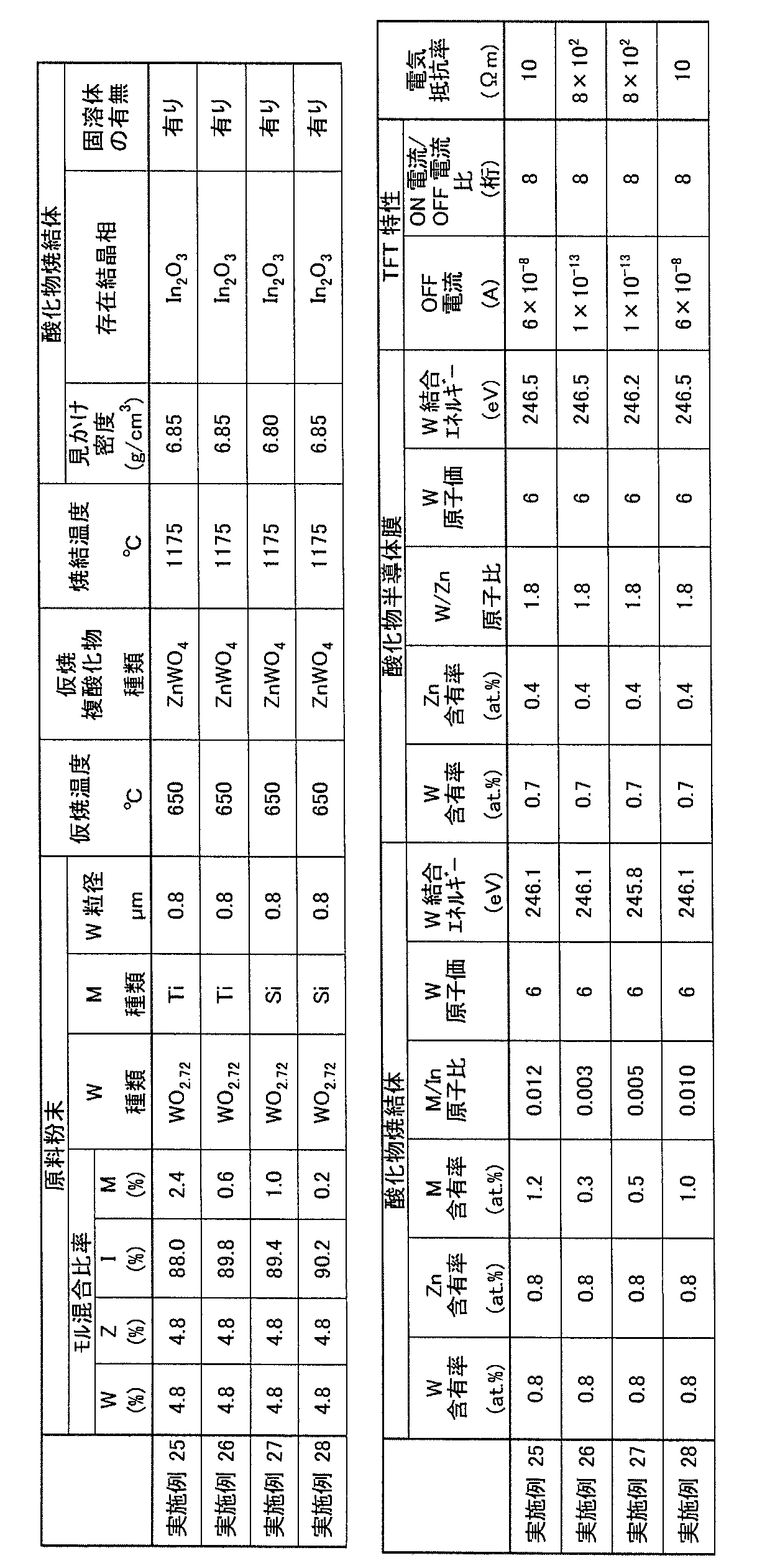
Claims (19)
- インジウムと、タングステンと、亜鉛と、を含む酸化物焼結体であって、
ビックスバイト型結晶相を主成分として含み、見かけ密度が6.5g/cm3より大きく7.1g/cm3以下であり、
前記酸化物焼結体中のインジウム、タングステンおよび亜鉛の合計に対するタングステンの含有率が1.2原子%より大きく30原子%より小さく、
前記酸化物焼結体中のインジウム、タングステンおよび亜鉛の合計に対する亜鉛の含有率が1.2原子%より大きく30原子%より小さい酸化物焼結体。 - 前記ビックスバイト型結晶相は、インジウム酸化物を主成分として含み、前記ビックスバイト型結晶相の少なくとも一部に固溶しているタングステンおよび亜鉛を含む請求項1に記載の酸化物焼結体。
- アルミニウム、チタン、クロム、ガリウム、ハフニウム、ジルコニウム、シリコン、モリブデン、バナジウム、ニオブ、タンタル、およびビスマスからなる群より選ばれる少なくとも1種の元素をさらに含み、
前記酸化物焼結体中におけるインジウム、タングステン、亜鉛および前記元素の合計に対する前記元素の含有率が0.1原子%以上10原子%以下である請求項1または請求項2に記載の酸化物焼結体。 - 前記酸化物焼結体中における、インジウムに対するシリコンの原子比が0.007より小さい、請求項3に記載の酸化物焼結体。
- 前記酸化物焼結体中における、インジウムに対するチタンの原子比が0.004より小さい、請求項3または請求項4に記載の酸化物焼結体。
- 6価および4価の少なくとも1つの原子価を有するタングステンを含む請求項1から請求項5のいずれか1項に記載の酸化物焼結体。
- X線光電子分光法により測定される結合エネルギーが245eV以上250eV以下のタングステンを含む請求項1から請求項5のいずれか1項に記載の酸化物焼結体。
- 請求項1から請求項7のいずれか1項に記載の酸化物焼結体を含むスパッタターゲット。
- 請求項8に記載のスパッタターゲットを用いてスパッタ法により形成した酸化物半導体膜を含む半導体デバイス。
- 前記酸化物半導体膜中のインジウム、タングステンおよび亜鉛の合計に対するタングステンの含有率が1.2原子%より大きく30原子%より小さく、
前記酸化物半導体膜中のインジウム、タングステンおよび亜鉛の合計に対する亜鉛の含有率が1.2原子%より大きく30原子%より小さい請求項9に記載の半導体デバイス。 - 前記酸化物半導体膜中における、亜鉛に対するタングステンの原子比が0.5より大きく3.0より小さい請求項9または請求項10に記載の半導体デバイス。
- 前記酸化物半導体膜中における、インジウムに対するシリコンの原子比が0.007より小さく、かつ前記酸化物半導体膜の電気抵抗率が1×10²Ωcm以上である請求項9から請求項11のいずれか1項に記載の半導体デバイス。
- 前記酸化物半導体膜中における、インジウムに対するチタンの原子比が0.004より小さく、かつ前記酸化物半導体膜の電気抵抗率が1×10²Ωcm以上である請求項9から請求項12のいずれか1項に記載の半導体デバイス。
- 前記酸化物半導体膜は、6価および4価の少なくとも1つの原子価を有するタングステンを含む請求項9から請求項13のいずれか1項に記載の半導体デバイス。
- 前記酸化物半導体膜は、X線光電子分光法により測定される結合エネルギーが245eV以上250eV以下のタングステンを含む請求項9から請求項13のいずれか1項に記載の半導体デバイス。
- 請求項1から請求項6のいずれか1項に記載の酸化物焼結体の製造方法であって、
亜鉛酸化物粉末とタングステン酸化物粉末との1次混合物を調製する工程と、
前記1次混合物を熱処理することにより仮焼粉末を形成する工程と、
前記仮焼粉末を含む原料粉末の2次混合物を調製する工程と、
前記2次混合物を成形することにより成形体を形成する工程と、
前記成形体を焼結することにより酸化物焼結体を形成する工程と、
を含み、
前記仮焼粉末を形成する工程は、酸素含有雰囲気下、550℃以上1200℃未満の温度で前記1次混合物を熱処理することにより、前記仮焼成粉末として亜鉛とタングステンとを含む複酸化物の粉末を形成することを含む酸化物焼結体の製造方法。 - 前記タングステン酸化物粉末は、WO3結晶相、WO2結晶相、およびWO2.72結晶相からなる群より選ばれる少なくとも1種の結晶相を含む請求項16に記載の酸化物焼結体の製造方法。
- 前記タングステン酸化物粉末のメジアン粒径d50が、0.1μm以上4μm以下である請求項16または請求項17に記載の酸化物焼結体の製造方法。
- 前記複酸化物がZnWO4型結晶相を含む請求項16から請求項18のいずれか1項に記載の酸化物焼結体の製造方法。
Priority Applications (6)
| Application Number | Priority Date | Filing Date | Title |
|---|---|---|---|
| US14/787,751 US9957604B2 (en) | 2014-03-25 | 2015-03-18 | Oxide sintered body and method for manufacturing the same, sputtering target, and semiconductor device |
| KR1020157032831A KR20150143812A (ko) | 2014-03-25 | 2015-03-18 | 산화물 소결체 및 그 제조 방법, 스퍼터 타겟, 그리고 반도체 디바이스 |
| KR1020177011334A KR102042905B1 (ko) | 2014-03-25 | 2015-03-18 | 산화물 소결체 및 그 제조 방법, 스퍼터 타겟, 그리고 반도체 디바이스 |
| EP15768922.5A EP2980041A4 (en) | 2014-03-25 | 2015-03-18 | Oxide sintered compact, method for manufacturing same, sputtering target, and semiconductor device |
| CN201580000813.3A CN105246856A (zh) | 2014-03-25 | 2015-03-18 | 氧化物烧结体及其制造方法、溅射靶和半导体器件 |
| US15/928,769 US10480060B2 (en) | 2014-03-25 | 2018-03-22 | Oxide sintered body and method for manufacturing the same, sputtering target, and semiconductor device |
Applications Claiming Priority (4)
| Application Number | Priority Date | Filing Date | Title |
|---|---|---|---|
| JP2014-061493 | 2014-03-25 | ||
| JP2014061493 | 2014-03-25 | ||
| JP2015-016695 | 2015-01-30 | ||
| JP2015016695A JP6119773B2 (ja) | 2014-03-25 | 2015-01-30 | 酸化物焼結体およびその製造方法、スパッタターゲット、ならびに半導体デバイス |
Related Child Applications (2)
| Application Number | Title | Priority Date | Filing Date |
|---|---|---|---|
| US14/787,751 A-371-Of-International US9957604B2 (en) | 2014-03-25 | 2015-03-18 | Oxide sintered body and method for manufacturing the same, sputtering target, and semiconductor device |
| US15/928,769 Division US10480060B2 (en) | 2014-03-25 | 2018-03-22 | Oxide sintered body and method for manufacturing the same, sputtering target, and semiconductor device |
Publications (1)
| Publication Number | Publication Date |
|---|---|
| WO2015146745A1 true WO2015146745A1 (ja) | 2015-10-01 |
Family
ID=54195267
Family Applications (1)
| Application Number | Title | Priority Date | Filing Date |
|---|---|---|---|
| PCT/JP2015/058061 WO2015146745A1 (ja) | 2014-03-25 | 2015-03-18 | 酸化物焼結体およびその製造方法、スパッタターゲット、ならびに半導体デバイス |
Country Status (7)
| Country | Link |
|---|---|
| US (2) | US9957604B2 (ja) |
| EP (1) | EP2980041A4 (ja) |
| JP (1) | JP6119773B2 (ja) |
| KR (2) | KR20150143812A (ja) |
| CN (1) | CN105246856A (ja) |
| TW (1) | TWI653352B (ja) |
| WO (1) | WO2015146745A1 (ja) |
Cited By (4)
| Publication number | Priority date | Publication date | Assignee | Title |
|---|---|---|---|---|
| WO2016129146A1 (ja) * | 2015-02-13 | 2016-08-18 | 住友電気工業株式会社 | 酸化物焼結体およびその製造方法、スパッタターゲット、ならびに半導体デバイス |
| JP2017224650A (ja) * | 2016-06-13 | 2017-12-21 | 住友電気工業株式会社 | 半導体デバイスおよびその製造方法 |
| US9957604B2 (en) | 2014-03-25 | 2018-05-01 | Sumitomo Electric Industries, Ltd. | Oxide sintered body and method for manufacturing the same, sputtering target, and semiconductor device |
| US10087517B2 (en) | 2014-10-22 | 2018-10-02 | Sumitomo Electric Industries, Ltd. | Oxide sintered body and semiconductor device |
Families Citing this family (7)
| Publication number | Priority date | Publication date | Assignee | Title |
|---|---|---|---|---|
| JP6809157B2 (ja) * | 2016-02-22 | 2021-01-06 | 東ソー株式会社 | 酸化物焼結体及び酸化物透明導電膜 |
| CN109906211B (zh) * | 2016-11-04 | 2022-04-01 | 住友电气工业株式会社 | 氧化物烧结材料及其制造方法、溅射靶和制造半导体器件的方法 |
| WO2018109970A1 (ja) * | 2016-12-12 | 2018-06-21 | 住友電気工業株式会社 | 半導体デバイスおよびその製造方法 |
| KR102401708B1 (ko) * | 2017-02-20 | 2022-05-26 | 스미토모덴키고교가부시키가이샤 | 산화물 소결체 및 그의 제조 방법, 스퍼터 타겟, 그리고 반도체 디바이스의 제조 방법 |
| CN110300738B (zh) * | 2017-02-20 | 2022-03-22 | 住友电气工业株式会社 | 氧化物烧结材料、制造氧化物烧结材料的方法、溅射靶和制造半导体器件的方法 |
| CN109994559B (zh) * | 2019-03-29 | 2021-07-23 | 吉林建筑大学 | 一种半导体氧化膜及其制备方法 |
| CN111943650B (zh) * | 2020-07-22 | 2022-11-29 | 长沙壹纳光电材料有限公司 | 一种用于活化等离子沉积技术的iwo靶材及其制备方法 |
Citations (6)
| Publication number | Priority date | Publication date | Assignee | Title |
|---|---|---|---|---|
| JP2002275623A (ja) * | 2001-03-19 | 2002-09-25 | Sumitomo Metal Mining Co Ltd | 透明導電性薄膜形成用焼結体ターゲット、その製造方法、及びそれより得られる透明導電性薄膜 |
| JP2004091265A (ja) * | 2002-08-30 | 2004-03-25 | Sumitomo Metal Mining Co Ltd | 酸化物焼結体 |
| JP2005314131A (ja) * | 2004-04-27 | 2005-11-10 | Sumitomo Metal Mining Co Ltd | 酸化物焼結体、スパッタリングターゲット、透明導電性薄膜およびその製造方法 |
| JP2006160535A (ja) * | 2004-12-02 | 2006-06-22 | Sumitomo Metal Mining Co Ltd | 酸化物焼結体、スパッタリングターゲットおよび透明導電性薄膜 |
| JP2006193363A (ja) * | 2005-01-12 | 2006-07-27 | Sumitomo Metal Mining Co Ltd | 酸化物焼結体、スパッタリングターゲットおよび透明導電性薄膜 |
| JP2010251604A (ja) * | 2009-04-17 | 2010-11-04 | Bridgestone Corp | 薄膜トランジスタの製造方法 |
Family Cites Families (25)
| Publication number | Priority date | Publication date | Assignee | Title |
|---|---|---|---|---|
| US8038857B2 (en) | 2004-03-09 | 2011-10-18 | Idemitsu Kosan Co., Ltd. | Thin film transistor, thin film transistor substrate, processes for producing the same, liquid crystal display using the same, and related devices and processes; and sputtering target, transparent electroconductive film formed by use of this, transparent electrode, and related devices and processes |
| JP2006022373A (ja) | 2004-07-07 | 2006-01-26 | Sumitomo Metal Mining Co Ltd | 透明導電性薄膜作製用スパッタリングターゲットの製造方法 |
| JP2006188392A (ja) * | 2005-01-06 | 2006-07-20 | Sumitomo Metal Mining Co Ltd | 酸化物焼結体、透明導電性薄膜およびその実装素子 |
| JP4760154B2 (ja) | 2005-06-15 | 2011-08-31 | 住友金属鉱山株式会社 | 酸化物焼結体、酸化物透明導電膜、およびこれらの製造方法 |
| JP2007153702A (ja) | 2005-12-07 | 2007-06-21 | Canon Inc | 亜鉛とタングステンからなる三斜晶系構造の複合酸化物および発光体 |
| JP4662075B2 (ja) | 2007-02-02 | 2011-03-30 | 株式会社ブリヂストン | 薄膜トランジスタ及びその製造方法 |
| KR101312259B1 (ko) | 2007-02-09 | 2013-09-25 | 삼성전자주식회사 | 박막 트랜지스터 및 그 제조방법 |
| JP5372776B2 (ja) * | 2007-12-25 | 2013-12-18 | 出光興産株式会社 | 酸化物半導体電界効果型トランジスタ及びその製造方法 |
| KR20130080063A (ko) | 2008-06-06 | 2013-07-11 | 이데미쓰 고산 가부시키가이샤 | 산화물 박막용 스퍼터링 타겟 및 그의 제조 방법 |
| JPWO2010070832A1 (ja) | 2008-12-15 | 2012-05-24 | 出光興産株式会社 | 複合酸化物焼結体及びそれからなるスパッタリングターゲット |
| CN102460712A (zh) | 2009-04-17 | 2012-05-16 | 株式会社普利司通 | 薄膜晶体管以及薄膜晶体管的制造方法 |
| US20120023188A1 (en) * | 2010-07-23 | 2012-01-26 | Martin Galaxia L | Private Profile Radio Channel |
| EP2671855B1 (en) | 2011-02-04 | 2016-05-25 | Sumitomo Metal Mining Co., Ltd. | Oxide sintered body and tablets obtained by processing same |
| JP2013001590A (ja) | 2011-06-15 | 2013-01-07 | Sumitomo Electric Ind Ltd | 導電性酸化物およびその製造方法、ならびに酸化物半導体膜 |
| JP2013173658A (ja) | 2012-02-27 | 2013-09-05 | Sumitomo Chemical Co Ltd | 酸化錫系焼結体およびその製造方法 |
| JP5772667B2 (ja) | 2012-03-06 | 2015-09-02 | 住友金属鉱山株式会社 | 蒸着用タブレットとその製造方法 |
| JP5966840B2 (ja) | 2012-10-11 | 2016-08-10 | 住友金属鉱山株式会社 | 酸化物半導体薄膜および薄膜トランジスタ |
| JP6137111B2 (ja) | 2013-10-23 | 2017-05-31 | 住友電気工業株式会社 | 酸化物焼結体および半導体デバイスの製造方法 |
| KR20150105527A (ko) | 2014-03-06 | 2015-09-17 | 삼성디스플레이 주식회사 | 산화물 스퍼터링 타겟 및 이를 이용한 박막 트랜지스터 |
| JP6119773B2 (ja) | 2014-03-25 | 2017-04-26 | 住友電気工業株式会社 | 酸化物焼結体およびその製造方法、スパッタターゲット、ならびに半導体デバイス |
| US20160251264A1 (en) * | 2014-08-12 | 2016-09-01 | Sumitomo Electric Industries, Ltd. | Oxide sintered body and method for manufacturing the same, sputtering target, and semiconductor device |
| KR101816468B1 (ko) * | 2014-10-22 | 2018-01-08 | 스미토모덴키고교가부시키가이샤 | 산화물 소결체 및 반도체 디바이스 |
| JP6551414B2 (ja) * | 2015-01-26 | 2019-07-31 | 住友電気工業株式会社 | 酸化物半導体膜および半導体デバイス |
| EP3257827A4 (en) * | 2015-02-13 | 2018-10-17 | Sumitomo Electric Industries, Ltd. | Oxide sintered body and method for producing same, sputter target, and semiconductor device |
| WO2017037564A1 (en) * | 2015-08-28 | 2017-03-09 | Semiconductor Energy Laboratory Co., Ltd. | Oxide semiconductor, transistor, and semiconductor device |
-
2015
- 2015-01-30 JP JP2015016695A patent/JP6119773B2/ja active Active
- 2015-03-18 KR KR1020157032831A patent/KR20150143812A/ko not_active Application Discontinuation
- 2015-03-18 EP EP15768922.5A patent/EP2980041A4/en not_active Withdrawn
- 2015-03-18 KR KR1020177011334A patent/KR102042905B1/ko active IP Right Grant
- 2015-03-18 CN CN201580000813.3A patent/CN105246856A/zh active Pending
- 2015-03-18 WO PCT/JP2015/058061 patent/WO2015146745A1/ja active Application Filing
- 2015-03-18 US US14/787,751 patent/US9957604B2/en active Active
- 2015-03-25 TW TW104109591A patent/TWI653352B/zh active
-
2018
- 2018-03-22 US US15/928,769 patent/US10480060B2/en active Active
Patent Citations (6)
| Publication number | Priority date | Publication date | Assignee | Title |
|---|---|---|---|---|
| JP2002275623A (ja) * | 2001-03-19 | 2002-09-25 | Sumitomo Metal Mining Co Ltd | 透明導電性薄膜形成用焼結体ターゲット、その製造方法、及びそれより得られる透明導電性薄膜 |
| JP2004091265A (ja) * | 2002-08-30 | 2004-03-25 | Sumitomo Metal Mining Co Ltd | 酸化物焼結体 |
| JP2005314131A (ja) * | 2004-04-27 | 2005-11-10 | Sumitomo Metal Mining Co Ltd | 酸化物焼結体、スパッタリングターゲット、透明導電性薄膜およびその製造方法 |
| JP2006160535A (ja) * | 2004-12-02 | 2006-06-22 | Sumitomo Metal Mining Co Ltd | 酸化物焼結体、スパッタリングターゲットおよび透明導電性薄膜 |
| JP2006193363A (ja) * | 2005-01-12 | 2006-07-27 | Sumitomo Metal Mining Co Ltd | 酸化物焼結体、スパッタリングターゲットおよび透明導電性薄膜 |
| JP2010251604A (ja) * | 2009-04-17 | 2010-11-04 | Bridgestone Corp | 薄膜トランジスタの製造方法 |
Non-Patent Citations (1)
| Title |
|---|
| See also references of EP2980041A4 * |
Cited By (11)
| Publication number | Priority date | Publication date | Assignee | Title |
|---|---|---|---|---|
| US9957604B2 (en) | 2014-03-25 | 2018-05-01 | Sumitomo Electric Industries, Ltd. | Oxide sintered body and method for manufacturing the same, sputtering target, and semiconductor device |
| US10480060B2 (en) | 2014-03-25 | 2019-11-19 | Sumitomo Electric Industries, Ltd. | Oxide sintered body and method for manufacturing the same, sputtering target, and semiconductor device |
| US10087517B2 (en) | 2014-10-22 | 2018-10-02 | Sumitomo Electric Industries, Ltd. | Oxide sintered body and semiconductor device |
| WO2016129146A1 (ja) * | 2015-02-13 | 2016-08-18 | 住友電気工業株式会社 | 酸化物焼結体およびその製造方法、スパッタターゲット、ならびに半導体デバイス |
| CN106164016A (zh) * | 2015-02-13 | 2016-11-23 | 住友电气工业株式会社 | 氧化物烧结体及其制造方法、溅射靶和半导体器件 |
| US20170069474A1 (en) | 2015-02-13 | 2017-03-09 | Sumitomo Electric Industries, Ltd. | Oxide sintered body and method for manufacturing the same, sputtering target, and semiconductor device |
| CN106164016B (zh) * | 2015-02-13 | 2019-08-09 | 住友电气工业株式会社 | 氧化物烧结体及其制造方法、溅射靶和半导体器件 |
| US10475631B2 (en) | 2015-02-13 | 2019-11-12 | Sumitomo Electric Industries, Ltd. | Oxide sintered body and method for manufacturing the same, sputtering target, and semiconductor device |
| US10811238B2 (en) | 2015-02-13 | 2020-10-20 | Sumitomo Electric Industries, Ltd. | Oxide sintered body and method for manufacturing the same, sputtering target, and semiconductor device |
| JP2017224650A (ja) * | 2016-06-13 | 2017-12-21 | 住友電気工業株式会社 | 半導体デバイスおよびその製造方法 |
| WO2017217007A1 (ja) * | 2016-06-13 | 2017-12-21 | 住友電気工業株式会社 | 半導体デバイスおよびその製造方法 |
Also Published As
| Publication number | Publication date |
|---|---|
| CN105246856A (zh) | 2016-01-13 |
| US20190093211A1 (en) | 2019-03-28 |
| US10480060B2 (en) | 2019-11-19 |
| KR20150143812A (ko) | 2015-12-23 |
| TWI653352B (zh) | 2019-03-11 |
| KR20170049630A (ko) | 2017-05-10 |
| KR102042905B1 (ko) | 2019-11-08 |
| EP2980041A4 (en) | 2017-01-11 |
| EP2980041A1 (en) | 2016-02-03 |
| TW201542848A (zh) | 2015-11-16 |
| JP6119773B2 (ja) | 2017-04-26 |
| US9957604B2 (en) | 2018-05-01 |
| US20170022602A1 (en) | 2017-01-26 |
| JP2015193525A (ja) | 2015-11-05 |
Similar Documents
| Publication | Publication Date | Title |
|---|---|---|
| JP6119773B2 (ja) | 酸化物焼結体およびその製造方法、スパッタターゲット、ならびに半導体デバイス | |
| JP6428780B2 (ja) | 酸化物焼結体およびその製造方法、スパッタターゲット、ならびに半導体デバイス | |
| JP6137111B2 (ja) | 酸化物焼結体および半導体デバイスの製造方法 | |
| JP6493502B2 (ja) | 酸化物焼結体の製造方法 | |
| WO2016063557A1 (ja) | 酸化物焼結体および半導体デバイス | |
| WO2017047152A1 (ja) | 酸化物焼結体およびその製造方法、スパッタターゲット、ならびに半導体デバイスの製造方法 | |
| JP6593268B2 (ja) | 酸化物焼結体およびその製造方法、スパッタターゲット、ならびに半導体デバイスの製造方法 | |
| JP6233447B2 (ja) | 酸化物焼結体およびその製造方法、スパッタターゲット、ならびに半導体デバイス | |
| JP6350466B2 (ja) | 酸化物焼結体およびその製造方法、スパッタターゲット、ならびに半導体デバイスの製造方法 | |
| JP6493501B2 (ja) | 酸化物焼結体の製造方法 | |
| WO2018083837A1 (ja) | 酸化物焼結体およびその製造方法、スパッタターゲット、ならびに半導体デバイスの製造方法 | |
| JP2016060686A (ja) | 酸化物焼結体およびその製造方法、スパッタリング用ターゲット、ならびに半導体デバイス | |
| JP6493601B2 (ja) | 酸化物焼結体およびその製造方法、スパッタターゲット、ならびに半導体デバイスの製造方法 | |
| JP6255813B2 (ja) | 酸化物焼結体および半導体デバイス |
Legal Events
| Date | Code | Title | Description |
|---|---|---|---|
| WWE | Wipo information: entry into national phase |
Ref document number: 201580000813.3 Country of ref document: CN |
|
| WWE | Wipo information: entry into national phase |
Ref document number: 14787751 Country of ref document: US |
|
| WWE | Wipo information: entry into national phase |
Ref document number: 2015768922 Country of ref document: EP |
|
| 121 | Ep: the epo has been informed by wipo that ep was designated in this application |
Ref document number: 15768922 Country of ref document: EP Kind code of ref document: A1 |
|
| ENP | Entry into the national phase |
Ref document number: 20157032831 Country of ref document: KR Kind code of ref document: A |
|
| NENP | Non-entry into the national phase |
Ref country code: DE |