WO2015146041A1 - 駆動装置 - Google Patents
駆動装置 Download PDFInfo
- Publication number
- WO2015146041A1 WO2015146041A1 PCT/JP2015/001366 JP2015001366W WO2015146041A1 WO 2015146041 A1 WO2015146041 A1 WO 2015146041A1 JP 2015001366 W JP2015001366 W JP 2015001366W WO 2015146041 A1 WO2015146041 A1 WO 2015146041A1
- Authority
- WO
- WIPO (PCT)
- Prior art keywords
- switching element
- current
- power switching
- circuit
- threshold value
- Prior art date
- Legal status (The legal status is an assumption and is not a legal conclusion. Google has not performed a legal analysis and makes no representation as to the accuracy of the status listed.)
- Ceased
Links
Images

Classifications
-
- H—ELECTRICITY
- H03—ELECTRONIC CIRCUITRY
- H03K—PULSE TECHNIQUE
- H03K17/00—Electronic switching or gating, i.e. not by contact-making and –breaking
- H03K17/08—Modifications for protecting switching circuit against overcurrent or overvoltage
- H03K17/082—Modifications for protecting switching circuit against overcurrent or overvoltage by feedback from the output to the control circuit
- H03K17/0828—Modifications for protecting switching circuit against overcurrent or overvoltage by feedback from the output to the control circuit in composite switches
-
- H—ELECTRICITY
- H02—GENERATION; CONVERSION OR DISTRIBUTION OF ELECTRIC POWER
- H02M—APPARATUS FOR CONVERSION BETWEEN AC AND AC, BETWEEN AC AND DC, OR BETWEEN DC AND DC, AND FOR USE WITH MAINS OR SIMILAR POWER SUPPLY SYSTEMS; CONVERSION OF DC OR AC INPUT POWER INTO SURGE OUTPUT POWER; CONTROL OR REGULATION THEREOF
- H02M1/00—Details of apparatus for conversion
- H02M1/08—Circuits specially adapted for the generation of control voltages for semiconductor devices incorporated in static converters
-
- H—ELECTRICITY
- H02—GENERATION; CONVERSION OR DISTRIBUTION OF ELECTRIC POWER
- H02M—APPARATUS FOR CONVERSION BETWEEN AC AND AC, BETWEEN AC AND DC, OR BETWEEN DC AND DC, AND FOR USE WITH MAINS OR SIMILAR POWER SUPPLY SYSTEMS; CONVERSION OF DC OR AC INPUT POWER INTO SURGE OUTPUT POWER; CONTROL OR REGULATION THEREOF
- H02M1/00—Details of apparatus for conversion
- H02M1/32—Means for protecting converters other than automatic disconnection
-
- H—ELECTRICITY
- H03—ELECTRONIC CIRCUITRY
- H03K—PULSE TECHNIQUE
- H03K17/00—Electronic switching or gating, i.e. not by contact-making and –breaking
- H03K17/16—Modifications for eliminating interference voltages or currents
- H03K17/168—Modifications for eliminating interference voltages or currents in composite switches
-
- H—ELECTRICITY
- H03—ELECTRONIC CIRCUITRY
- H03K—PULSE TECHNIQUE
- H03K17/00—Electronic switching or gating, i.e. not by contact-making and –breaking
- H03K17/51—Electronic switching or gating, i.e. not by contact-making and –breaking characterised by the components used
- H03K17/56—Electronic switching or gating, i.e. not by contact-making and –breaking characterised by the components used by the use, as active elements, of semiconductor devices
- H03K17/567—Circuits characterised by the use of more than one type of semiconductor device, e.g. BIMOS, composite devices such as IGBT
-
- H—ELECTRICITY
- H03—ELECTRONIC CIRCUITRY
- H03K—PULSE TECHNIQUE
- H03K17/00—Electronic switching or gating, i.e. not by contact-making and –breaking
- H03K17/51—Electronic switching or gating, i.e. not by contact-making and –breaking characterised by the components used
- H03K17/56—Electronic switching or gating, i.e. not by contact-making and –breaking characterised by the components used by the use, as active elements, of semiconductor devices
- H03K17/687—Electronic switching or gating, i.e. not by contact-making and –breaking characterised by the components used by the use, as active elements, of semiconductor devices the devices being field-effect transistors
- H03K17/6877—Electronic switching or gating, i.e. not by contact-making and –breaking characterised by the components used by the use, as active elements, of semiconductor devices the devices being field-effect transistors the control circuit comprising active elements different from those used in the output circuit
-
- H—ELECTRICITY
- H02—GENERATION; CONVERSION OR DISTRIBUTION OF ELECTRIC POWER
- H02M—APPARATUS FOR CONVERSION BETWEEN AC AND AC, BETWEEN AC AND DC, OR BETWEEN DC AND DC, AND FOR USE WITH MAINS OR SIMILAR POWER SUPPLY SYSTEMS; CONVERSION OF DC OR AC INPUT POWER INTO SURGE OUTPUT POWER; CONTROL OR REGULATION THEREOF
- H02M1/00—Details of apparatus for conversion
- H02M1/0003—Details of control, feedback or regulation circuits
- H02M1/0009—Devices or circuits for detecting current in a converter
-
- H—ELECTRICITY
- H02—GENERATION; CONVERSION OR DISTRIBUTION OF ELECTRIC POWER
- H02M—APPARATUS FOR CONVERSION BETWEEN AC AND AC, BETWEEN AC AND DC, OR BETWEEN DC AND DC, AND FOR USE WITH MAINS OR SIMILAR POWER SUPPLY SYSTEMS; CONVERSION OF DC OR AC INPUT POWER INTO SURGE OUTPUT POWER; CONTROL OR REGULATION THEREOF
- H02M1/00—Details of apparatus for conversion
- H02M1/0003—Details of control, feedback or regulation circuits
- H02M1/0029—Circuits or arrangements for limiting the slope of switching signals, e.g. slew rate
-
- H—ELECTRICITY
- H03—ELECTRONIC CIRCUITRY
- H03K—PULSE TECHNIQUE
- H03K17/00—Electronic switching or gating, i.e. not by contact-making and –breaking
- H03K17/16—Modifications for eliminating interference voltages or currents
- H03K17/161—Modifications for eliminating interference voltages or currents in field-effect transistor switches
- H03K17/162—Modifications for eliminating interference voltages or currents in field-effect transistor switches without feedback from the output circuit to the control circuit
- H03K17/163—Soft switching
Definitions
- This disclosure relates to a drive device that performs on / off control of a power switching element and protection in case of an abnormality.
- the protection circuit described in Patent Document 1 reduces the gate voltage of the power switching element by resistance voltage division and suppresses the current. And when the electric current more than the threshold value for short circuit detection is flowing continuously for the predetermined time, it judges that it is a short circuit of a load and stops the drive of a power switching element.
- the waveform of the gate voltage is distorted by the voltage dividing resistor and the gate capacitance of the power switching element, and the time constant when the gate voltage is suppressed becomes large. For this reason, the time required for reducing the current of the power switching element becomes long, and the stress is large.
- the power conversion device described in Patent Document 2 employs a method in which the gate voltage of the power switching element is suppressed by a Zener diode when a short circuit is detected.
- the gate voltage can be sharply reduced, and the problem of the time constant when the gate voltage is suppressed can be solved.
- Zener diodes have large variations in characteristics due to temperature and manufacturing variations, and cannot solve the problem of erroneous release of the short-circuit protection operation.
- This disclosure is intended to protect and control a gate voltage appropriately when an excessive current flows due to a load short circuit in a drive device that performs on / off control of a power switching element and protection in case of abnormality.
- a driving device configured to control a gate current of a power switching element that drives a load and to turn on the power switching element; and to connect a main power source in series with the on-side circuit, and the power switching element
- An off-side circuit for turning off the power, and a gate of the power switching element is connected to an intermediate point between the on-side circuit and the off-side circuit, and the power switching element based on a current value of a collector current of the power switching element
- a protection circuit for controlling the gate current of the transistor.
- the protection circuit includes a constant current circuit that defines a constant current for extracting the gate charge of the power switching element, a protection switch that controls electrical connection between the constant current circuit and the gate of the power switching element, And a collector current detector for detecting that the current value of the collector current of the power switching element exceeds a predetermined threshold value.
- the collector current detection unit turns off the on-side circuit and turns off the power after a predetermined time from when the current value of the collector current of the power switching element exceeds a first threshold value indicating a short circuit of the load as a predetermined threshold value.
- the switching element is disconnected from the main power source and the protection switch is turned on.
- a constant current circuit is provided as an extraction destination when an electric charge is extracted from the gate of the power switching element. For this reason, the gate charge of the power switching element is extracted at a constant speed. In other words, the gate voltage and thus the collector current can be reduced at a constant slew rate. Therefore, it is possible to suppress the rounding of the waveform of the gate voltage and thus the collector current, and ringing due to a sudden decrease in these voltage and current.
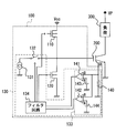
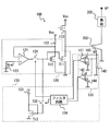
- FIG. 1 is a circuit diagram showing a schematic configuration of the driving apparatus according to the first embodiment.
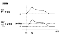
- FIG. 2 is a timing chart showing driving of the driving device in the conventional configuration.
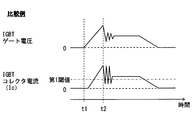
- FIG. 3 is a timing chart showing driving of the driving device in the conventional configuration.
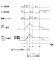
- FIG. 4 is a timing chart showing driving of the driving apparatus according to the first embodiment.
- FIG. 5 is a timing chart showing driving of the driving device according to the first modification.
- FIG. 6 is a circuit diagram illustrating a schematic configuration of the driving apparatus according to the second embodiment.
- the driving apparatus 100 controls driving of an insulated gate bipolar transistor (IGBT) 200 as a power switching element that drives a load 300.
- IGBT insulated gate bipolar transistor
- the driving device 100 includes an on-side circuit 110, an off-side circuit 120, and a protection circuit 130.
- the on-side circuit 110 and the off-side circuit 120 are connected in series between the main power supply and GND, and the gate of the IGBT 200 is connected to the middle point thereof.
- the on-side circuit 110 is composed of a PMOS transistor, and when the PMOS transistor is in an on state, the power supply voltage Vcc is applied to the gate of the IGBT 200. As a result, the IGBT 200 is turned on, a current flows between the collector and the emitter of the IGBT 200, and power is supplied to the load 300.
- the off-side circuit 120 is constituted by an NMOS transistor, and when the NMOS transistor is in an on state, charges are extracted from the gate of the IGBT 200 and the IGBT 200 is in an off state.
- the protection circuit 130 controls the gate current and thus the gate voltage of the IGBT 200 based on the collector current Ic of the IGBT 200.
- the protection circuit 130 controls the electrical connection between the constant current circuit 131 and the IGBT 200 by pulling out the gate charge of the IGBT 200 at a constant rate, and enables / disables the constant current circuit 131.
- a protective switch 132 to be defined and a collector current detector 133 that detects the collector current Ic of the IGBT 200 are provided.
- the collector current detection unit 133 is a circuit that detects an abnormality in the collector current of the IGBT 200 due to a short circuit of the load 300.
- the collector current detection unit 133 includes a resistor 140 for converting the collector current Ic of the IGBT 200 into a voltage, comparators 141 and 142, and a voltage source 143 that applies a threshold voltage to the input terminal A of the comparators 141 and 142. 144.
- a voltage source 143 is connected to one input terminal A of the comparator 141.
- the other input terminal B is connected to an intermediate point between the resistor 140 connected between the sense emitter terminal SE and GND of the IGBT 200. That is, a voltage corresponding to the current flowing from the sense emitter terminal SE of the IGBT 200 toward the GND and the resistance value of the resistor 140 is applied to the input terminal B of the comparator 141.
- the voltage applied to the input terminal B is proportional to the current flowing from the sense emitter terminal SE toward GND. That is, this voltage becomes higher as the collector current of the IGBT 200 increases.
- the protection switch 132 is turned on via a filter circuit 134 described later, and a control signal is output so that the on-side circuit 110 is turned off.
- the comparator 142 has the same configuration as the comparator 141. That is, the voltage source 144 is connected to one input terminal A of the comparator 142. The other input terminal B is connected to an intermediate point between the resistor 140 connected between the sense emitter terminal SE and GND of the IGBT 200.
- the voltage source 143 is set to a voltage that determines that the load 300 is in a short-circuit state for the IGBT 200, and defines the first threshold value. Further, the voltage source 144 is set to a voltage higher than the first threshold value and defines the second threshold value.
- the above-described filter circuit 134 is a circuit that outputs a control signal corresponding to the input after a predetermined filter time set in advance after the signal is input.
- the filter circuit 134 in the present embodiment when the collector current Ic of the IGBT 200 exceeds the first threshold, the filter circuit 134 in the present embodiment outputs a control signal so as to turn on the off-side circuit 120 after a preset first filter time.
- the filter circuit 134 turns on the protection switch 132 and turns off the on-side circuit 110 after a preset second filter time. Output.
- the filter circuit 134 is controlled to turn off the protection switch 132 after a preset third filter time when the collector current Ic of the IGBT 200 reaches the second threshold value from a state higher than the second threshold value. Output a signal.
- the third filter time is set to zero for convenience. That is, the filter circuit 134 outputs a control signal so as to turn off the protection switch 132 at the same time when the collector current Ic of the IGBT 200 reaches the second threshold value from a state where it is higher than the second threshold value.
- the filter circuit 134 is provided to prevent the protection circuit 130 from operating erroneously due to switching noise of the IGBT 200 or the like.
- the protection circuit described in Patent Document 1 employs a method in which the value of the gate voltage after being lowered is defined by resistance voltage division. For this reason, as shown in FIG. 2, even when the protection circuit operates at time t2 and the gate voltage starts to decrease, the collector current Ic is maintained in a large state due to the long time constant. As a result, the stress on the IGBT 200 is increased. In addition, since the gate voltage value is regulated to a constant value by resistance voltage division, the gate current varies due to variations in the gate capacitance of the IGBT 200.
- the power conversion device described in Patent Document 2 employs a method in which the value of the gate voltage is defined by a Zener diode. For this reason, as shown in FIG. 3, when the protection circuit operates at time t2, the gate voltage rapidly decreases and ringing occurs in the gate voltage and the collector current Ic. When ringing occurs in the collector current Ic, a large surge voltage is applied to the collector voltage.
- the IGBT 200 before the time t1, the IGBT 200 is in an off state. That is, the off-side circuit 120 is in an on (valid) state and the on-side circuit 110 is in an off (invalid) state, and no voltage is applied to the gate of the IGBT 200.
- the filter circuit 134 starts counting the first filter time.
- the counting of the second filter time is started simultaneously with the counting of the first filter time.
- the protection switch 132 is turned on and the on-side circuit 110 is turned off.
- the gate of the IGBT 200 is disconnected from the main power supply and GND, and the gate charge is extracted only by the constant current circuit 131.
- the charge is extracted from the gate by the constant current circuit 131 at a constant speed.
- the gate voltage can be reduced at a constant slew rate. Therefore, it is possible to suppress the ringing of the waveform of the gate voltage and the ringing due to the rapid decrease of the gate voltage.
- the protection switch 132 When the gate current falls from a state higher than the second threshold value and reaches the second threshold value (time t3) due to the charge being extracted from the gate of the IGBT 200, the protection switch 132 is turned off. As a result, the gate of the IGBT 200 is electrically floating. If the short circuit of the load 300 is false, the collector current Ic falls below the first threshold value, so the on-side circuit 110 is turned on and the IGBT 200 returns to normal operation. When the short circuit of the load 300 is true, the gate voltage is constant and the collector current Ic also maintains a constant value.
- the off-side circuit 120 is turned on, and the IGBT 200 stops its operation. Thereby, the IGBT 200 is protected from an excessive current.
- the collector current detection unit 133 monitors the collector current Ic of the IGBT 200, and the gate is brought into a floating state when the current value reaches the second threshold value. Therefore, the collector current Ic depends on the gate capacitance variation of the IGBT 200. Can be kept constant without. That is, even after the protection switch 132 is turned off, variations in the collector current Ic can be suppressed.
- the second threshold value can be set as close as possible to the first threshold value. When the second threshold value is larger than the first threshold value, the collector current Ic is maintained in a high state, and the stress on the IGBT 200 increases.
- the second threshold value can be made closer to the first threshold value as compared with the conventional configuration, the stress on the IGBT 200 can be reduced.
- the threshold value of the collector current Ic includes the first threshold value indicating a short circuit of the load 300 and the second threshold value set to a value higher than the first threshold value.
- a third threshold value having a higher current value than the second threshold value may be set.
- the first filter time for turning on the off-side circuit 120 and the second filter time for turning on the protection switch 132 are counted.
- the collector current Ic exceeds the first threshold only the first filter time starts counting.
- the collector current Ic exceeds the third threshold counting of the fourth filter time for turning on the protection switch 132 is started.
- the threshold value for turning on the protection switch 132 for protecting the IGBT 200 is set to the third threshold value that is higher than the first threshold value and the second threshold value, the collector current Ic exceeds the first threshold value. Even when a pulse noise is generated, the protection switch 132 can be prevented from being turned on by mistake. Therefore, the noise tolerance can be improved compared to the first embodiment.
- Modification 2 In the case where the off-side circuit 120 is turned on after the time when the protection switch 132 is turned on, it is preferable to reduce the drive capability of the off-side circuit 120 compared to the case where the protection switch 132 is not turned on. That is, for example, in FIG. 4, when the off-side circuit 120 is turned on at time t4 after time t2 when the protection switch 132 is operated, the protection switch 132 does not operate, that is, the normal drive in which the load 300 is not short-circuited. Compared to the case, it is preferable to reduce the drive capability of the off-side circuit 120.
- the collector current Ic of the IGBT 200 greatly exceeds the rating. For this reason, if the off-side circuit 120 is turned on with the same drive capability as that of the normal operation, the collector voltage may rapidly increase and an excessive surge voltage may be generated, which causes a failure of the IGBT 200. As described above, when the short circuit occurs in the load 300 and the protection switch 132 operates, the drive capability of the off-side circuit 120 is reduced compared to the normal driving in which the load 300 is not short-circuited. Therefore, the collector voltage surge can be suppressed.
- the gate charge of the IGBT 200 is extracted by the constant current circuit 131, and at the same time, a voltage in the vicinity of the threshold voltage is applied to the gate of the MOS transistor constituting the on-side circuit 110.
- a small current is supplied from the main power source to the gate. According to this, the slew rate of the gate current and the gate voltage can be reduced, and the undershoot accompanying the decrease in these currents and voltages can be suppressed. Therefore, it is possible to suppress variations in the collector current Ic after the time t3 as compared with the first embodiment and its modification.
- the protection circuit 130 may be configured to be able to control the gate current of the IGBT 200 based on the collector current Ic.
- the gate current of the IGBT 200 may be extracted via the off-side circuit 120.
- the collector current detection unit 133 and the filter circuit 134 have the same configuration as that of the first embodiment, and thus the description thereof is omitted.
- the driving device 100 has two NMOS transistors (Tr1, Tr2) as the off-side circuit 120. These NMOS transistors are composed of a main MOS transistor Tr1 as an output transistor and a sense MOS transistor Tr2 that defines the drain current of the main MOS transistor Tr1.
- the main MOS transistor Tr1 forms a current mirror with respect to the sense MOS transistor Tr2.
- the gate of the main MOS transistor Tr1 is common to the gate of the sense MOS transistor Tr2, and the source is commonly connected to GND.
- the drain of the main MOS transistor Tr1 is connected to the gate of the IGBT 200.
- the drain current flows through the main MOS transistor Tr1 at the same current ratio as that of the sense MOS transistor Tr2.
- the off-side circuit 120 includes an operational amplifier 121 for controlling the drain current of the sense MOS transistor Tr2, a reference resistor 122 for defining the output of the operational amplifier 121, and a reference potential at one input terminal of the operational amplifier 121. And a reference power supply 123 for providing Vref.
- the operational amplifier 121 applies a voltage to the gate of the sense MOS transistor Tr2 so that a constant current is drawn from the gate of the IGBT 200. It has become.
- the reference resistor 122 is a shunt resistor and defines the current value of the drain current of the sense MOS transistor Tr2. As a result, the current value of the current drawn from the gate of the IGBT 200 is defined.
- the current drawn from the gate of the IGBT 200 is a drain current flowing through the main MOS transistor Tr1. Since the main MOS transistor Tr1 forms a current mirror together with the sense MOS transistor Tr2, the current drawn from the gate of the IGBT 200 depends on the drain current of the sense MOS transistor Tr2.
- the operational amplifier 121 when a control signal indicating turning off the IGBT 200 is input, the operational amplifier 121 is driven and a gate voltage is applied to the sense MOS transistor Tr2.
- the drain current at this time is defined by the resistance value R of the reference resistor 122.
- the current value is feedback-controlled by adjusting the output of the operational amplifier 121 so that the potential at the connection point between the reference resistor 122 and the sense MOS transistor Tr2 approaches the reference potential Vref.
- the off-side circuit 120 includes a control switch 124 that turns on / off current supply to the main MOS transistor Tr1 by the operational amplifier 121. If the control switch 124 is on, a gate voltage is applied from the operational amplifier 121 to the sense MOS transistor Tr2, and the off-side circuit 120 is turned on.
- the driving device 100 includes a constant current circuit 131 as in the first embodiment.
- the constant current circuit 131 in this embodiment is connected to supply a drain current to the main MOS transistor Tr1 and the NMOS transistor Tr3 constituting the current mirror in the off-side circuit 120.
- the gates of the main MOS transistor Tr1 and the NMOS transistor Tr3 are connected via a switch. When this switch is on, the main MOS transistor Tr1 and the NMOS transistor Tr3 form a current mirror, and the current defined by the constant current circuit 131 flows as the drain current of Tr1, and draws out the gate charge of the IGBT 200. ing. That is, this switch corresponds to the protection switch 132 in the first embodiment and the modification thereof described above.
- one NMOS transistor is used for drawing the gate current from the IGBT 200 for protection by the protection circuit 130 and for drawing the gate current from the IGBT 200 for the off operation by the off-side circuit 120. That is, the main MOS transistor Tr1 can be shared.
- the first threshold value and the second threshold value are set to values corresponding to the collector current of the power switching element measured in advance under a constant gate voltage.
- the drive device 100 is provided with a memory circuit, and a threshold value corresponding to the voltage of the sense emitter terminal SE with respect to a predetermined collector current Ic of the IGBT 200 measured in a pre-shipment inspection (characteristic inspection performed after manufacture) of the drive device 100 Is stored in the memory.
- the higher the voltage at the sense emitter terminal SE the larger the values of the first threshold value and the second threshold value can be set, and it is possible to prevent malfunction caused by erroneous short circuit protection operation due to noise during normal switching operation.
- the second threshold value can be set as close as possible to the first threshold value, the stress of the IGBT 200 can be reduced.
- the protective operation when the load 300 is short-circuited has been described.
- an excessive current exceeding the rating of the collector of the IGBT 200 flows even though it is not as short as the load 300 is short-circuited.
- the present disclosure can be applied even in an overcurrent state.
- the first threshold value, the second threshold value, and the third threshold value are set to smaller values than in the case of a short circuit.
- the IGBT 200 is exemplified as the power switching element, but is not limited to this example.
- the present disclosure can be applied to a power MOS transistor or the like as a power switching element.
Landscapes
- Engineering & Computer Science (AREA)
- Power Engineering (AREA)
- Power Conversion In General (AREA)
- Electronic Switches (AREA)
- Metal-Oxide And Bipolar Metal-Oxide Semiconductor Integrated Circuits (AREA)
Priority Applications (2)
| Application Number | Priority Date | Filing Date | Title |
|---|---|---|---|
| CN201580015852.0A CN106134050B (zh) | 2014-03-27 | 2015-03-12 | 驱动装置 |
| US15/117,480 US9660636B2 (en) | 2014-03-27 | 2015-03-12 | Drive device |
Applications Claiming Priority (2)
| Application Number | Priority Date | Filing Date | Title |
|---|---|---|---|
| JP2014-066597 | 2014-03-27 | ||
| JP2014066597A JP6349856B2 (ja) | 2014-03-27 | 2014-03-27 | 駆動装置 |
Publications (1)
| Publication Number | Publication Date |
|---|---|
| WO2015146041A1 true WO2015146041A1 (ja) | 2015-10-01 |
Family
ID=54194595
Family Applications (1)
| Application Number | Title | Priority Date | Filing Date |
|---|---|---|---|
| PCT/JP2015/001366 Ceased WO2015146041A1 (ja) | 2014-03-27 | 2015-03-12 | 駆動装置 |
Country Status (4)
| Country | Link |
|---|---|
| US (1) | US9660636B2 (enExample) |
| JP (1) | JP6349856B2 (enExample) |
| CN (1) | CN106134050B (enExample) |
| WO (1) | WO2015146041A1 (enExample) |
Cited By (3)
| Publication number | Priority date | Publication date | Assignee | Title |
|---|---|---|---|---|
| CN107846137A (zh) * | 2016-09-19 | 2018-03-27 | 力博特公司 | 一种半导体开关元器件的限流方法及设备 |
| JPWO2017195247A1 (ja) * | 2016-05-09 | 2018-10-04 | 株式会社日立製作所 | 電力変換装置の診断システム、半導体モジュールの診断方法、および、電力変換装置 |
| CN112904925A (zh) * | 2019-11-19 | 2021-06-04 | 杭州海康消防科技有限公司 | 负载驱动和保护电路 |
Families Citing this family (10)
| Publication number | Priority date | Publication date | Assignee | Title |
|---|---|---|---|---|
| JP2018157617A (ja) * | 2017-03-15 | 2018-10-04 | トヨタ自動車株式会社 | ゲート電位制御装置 |
| JP2019057982A (ja) * | 2017-09-20 | 2019-04-11 | 株式会社東芝 | 半導体素子の駆動回路及び半導体素子の駆動方法 |
| JP7026531B2 (ja) * | 2018-02-23 | 2022-02-28 | ルネサスエレクトロニクス株式会社 | 半導体装置、半導体システム、及び、制御システム |
| JP6924216B2 (ja) * | 2019-03-05 | 2021-08-25 | 株式会社東芝 | 電子回路および方法 |
| CN110834653B (zh) * | 2019-10-15 | 2024-03-19 | 上海新海信通信息技术有限公司 | 城市轨道交通钢轨断轨监测系统及方法 |
| DE102022133711A1 (de) * | 2022-12-16 | 2024-06-27 | Infineon Technologies Ag | Intelligenter halbleiterschalter mit quasi-digitaler strombegrenzung |
| CN116248098A (zh) * | 2022-12-30 | 2023-06-09 | 华灿光电(浙江)有限公司 | 栅极驱动电路及方法 |
| US20240297643A1 (en) * | 2023-03-02 | 2024-09-05 | Texas Instruments Incorporated | Driver circuit with overcurrent protection |
| CN117791493A (zh) * | 2023-12-26 | 2024-03-29 | 上海贝岭股份有限公司 | 高边开关芯片 |
| US20250330170A1 (en) * | 2024-04-17 | 2025-10-23 | Texas Instruments Incorporated | High-side switch circuit |
Citations (5)
| Publication number | Priority date | Publication date | Assignee | Title |
|---|---|---|---|---|
| JP2010154595A (ja) * | 2008-12-24 | 2010-07-08 | Denso Corp | 電力変換装置 |
| JP2012023899A (ja) * | 2010-07-15 | 2012-02-02 | Fuji Electric Co Ltd | 電力用半導体素子のゲート駆動回路 |
| JP2012105088A (ja) * | 2010-11-10 | 2012-05-31 | Denso Corp | 電子装置 |
| JP2013102694A (ja) * | 2013-03-05 | 2013-05-23 | Denso Corp | 電子装置 |
| JP2013169102A (ja) * | 2012-02-16 | 2013-08-29 | Denso Corp | ゲート駆動回路 |
Family Cites Families (27)
| Publication number | Priority date | Publication date | Assignee | Title |
|---|---|---|---|---|
| JP2643459B2 (ja) | 1989-07-06 | 1997-08-20 | 三菱電機株式会社 | パワーデバイスの駆動・保護回路 |
| US5500619A (en) | 1992-03-18 | 1996-03-19 | Fuji Electric Co., Ltd. | Semiconductor device |
| JPH05276761A (ja) * | 1992-03-19 | 1993-10-22 | Hitachi Ltd | パワー半導体素子の過電流検出方法及び回路並びにこれを用いたインバータ装置 |
| JP3152204B2 (ja) | 1998-06-02 | 2001-04-03 | 日本電気株式会社 | スルーレート出力回路 |
| JP2001223571A (ja) | 2000-02-10 | 2001-08-17 | Fuji Electric Co Ltd | 電圧駆動型半導体素子のゲート駆動装置 |
| US7132868B2 (en) | 2001-06-27 | 2006-11-07 | Mitsubishi Denki Kabushiki Kaisha | Semiconductor device |
| DE10161743B4 (de) * | 2001-12-15 | 2004-08-05 | Hüttinger Elektronik GmbH & Co. KG | Hochfrequenzanregungsanordnung |
| JP4068022B2 (ja) * | 2003-07-16 | 2008-03-26 | Necエレクトロニクス株式会社 | 過電流検出回路及び負荷駆動回路 |
| US7106105B2 (en) * | 2004-07-21 | 2006-09-12 | Fairchild Semiconductor Corporation | High voltage integrated circuit driver with a high voltage PMOS bootstrap diode emulator |
| JP4619812B2 (ja) | 2005-02-16 | 2011-01-26 | 株式会社東芝 | ゲート駆動回路 |
| US7675346B2 (en) * | 2006-07-11 | 2010-03-09 | Delphi Technologies, Inc. | Switching control system to reduce coil output voltage when commencing coil charging |
| JP2010193431A (ja) * | 2009-01-26 | 2010-09-02 | Rohm Co Ltd | 出力回路およびモータ駆動装置 |
| JP2012070263A (ja) | 2010-09-24 | 2012-04-05 | Denso Corp | 電子装置 |
| JP5569460B2 (ja) | 2011-04-21 | 2014-08-13 | 株式会社デンソー | 負荷駆動装置 |
| DE102012204576A1 (de) * | 2012-03-22 | 2013-09-26 | Continental Automotive Gmbh | Vorrichtung zum Laden und Entladen eines kapazitiven Stellgliedes und Anordnung mit einer solchen Vorrichtung |
| US9087707B2 (en) * | 2012-03-26 | 2015-07-21 | Infineon Technologies Austria Ag | Semiconductor arrangement with a power transistor and a high voltage device integrated in a common semiconductor body |
| JP5632885B2 (ja) * | 2012-08-31 | 2014-11-26 | 株式会社日本自動車部品総合研究所 | 電力変換装置 |
| DE102013217037B3 (de) * | 2013-08-27 | 2014-12-11 | Continental Automotive Gmbh | Vorrichtung zum Laden und Entladen eines kapazitiven Stellgliedes und Anordnung mit einer solchen Vorrichtung |
| JP5915615B2 (ja) * | 2013-10-09 | 2016-05-11 | トヨタ自動車株式会社 | 半導体制御装置、スイッチング装置、インバータ及び制御システム |
| JP5831528B2 (ja) * | 2013-10-31 | 2015-12-09 | トヨタ自動車株式会社 | 半導体装置 |
| JP5831527B2 (ja) * | 2013-10-31 | 2015-12-09 | トヨタ自動車株式会社 | 半導体装置 |
| JP5800006B2 (ja) * | 2013-10-31 | 2015-10-28 | トヨタ自動車株式会社 | 半導体装置 |
| US9601985B2 (en) * | 2014-04-30 | 2017-03-21 | Nxp Usa, Inc. | Segmented driver for a transistor device |
| US9431386B2 (en) * | 2014-05-22 | 2016-08-30 | Avago Technologies General Ip (Singapore) Pte. Ltd. | Current sensing of emitter sense insulated-gate bipolar transistor (IGBT) |
| JP6422278B2 (ja) * | 2014-09-19 | 2018-11-14 | ルネサスエレクトロニクス株式会社 | 電力制御回路 |
| JP6396730B2 (ja) * | 2014-09-19 | 2018-09-26 | ルネサスエレクトロニクス株式会社 | 半導体装置 |
| JP6345583B2 (ja) * | 2014-12-03 | 2018-06-20 | ルネサスエレクトロニクス株式会社 | 半導体装置 |
-
2014
- 2014-03-27 JP JP2014066597A patent/JP6349856B2/ja active Active
-
2015
- 2015-03-12 US US15/117,480 patent/US9660636B2/en active Active
- 2015-03-12 WO PCT/JP2015/001366 patent/WO2015146041A1/ja not_active Ceased
- 2015-03-12 CN CN201580015852.0A patent/CN106134050B/zh active Active
Patent Citations (5)
| Publication number | Priority date | Publication date | Assignee | Title |
|---|---|---|---|---|
| JP2010154595A (ja) * | 2008-12-24 | 2010-07-08 | Denso Corp | 電力変換装置 |
| JP2012023899A (ja) * | 2010-07-15 | 2012-02-02 | Fuji Electric Co Ltd | 電力用半導体素子のゲート駆動回路 |
| JP2012105088A (ja) * | 2010-11-10 | 2012-05-31 | Denso Corp | 電子装置 |
| JP2013169102A (ja) * | 2012-02-16 | 2013-08-29 | Denso Corp | ゲート駆動回路 |
| JP2013102694A (ja) * | 2013-03-05 | 2013-05-23 | Denso Corp | 電子装置 |
Cited By (5)
| Publication number | Priority date | Publication date | Assignee | Title |
|---|---|---|---|---|
| JPWO2017195247A1 (ja) * | 2016-05-09 | 2018-10-04 | 株式会社日立製作所 | 電力変換装置の診断システム、半導体モジュールの診断方法、および、電力変換装置 |
| CN107846137A (zh) * | 2016-09-19 | 2018-03-27 | 力博特公司 | 一种半导体开关元器件的限流方法及设备 |
| CN107846137B (zh) * | 2016-09-19 | 2020-04-03 | 维谛公司 | 一种半导体开关元器件的限流方法及设备 |
| CN112904925A (zh) * | 2019-11-19 | 2021-06-04 | 杭州海康消防科技有限公司 | 负载驱动和保护电路 |
| CN112904925B (zh) * | 2019-11-19 | 2022-07-29 | 杭州海康消防科技有限公司 | 负载驱动和保护电路 |
Also Published As
| Publication number | Publication date |
|---|---|
| JP2015192491A (ja) | 2015-11-02 |
| US9660636B2 (en) | 2017-05-23 |
| CN106134050B (zh) | 2019-08-16 |
| US20160352319A1 (en) | 2016-12-01 |
| JP6349856B2 (ja) | 2018-07-04 |
| CN106134050A (zh) | 2016-11-16 |
Similar Documents
| Publication | Publication Date | Title |
|---|---|---|
| JP6349856B2 (ja) | 駆動装置 | |
| JP6164429B2 (ja) | 過電流保護電源装置 | |
| CN106134051B (zh) | 驱动装置 | |
| JP5315026B2 (ja) | 半導体装置 | |
| JP6197685B2 (ja) | ゲート駆動回路 | |
| KR101311690B1 (ko) | 단락 검출 회로 및 단락 검출 방법 | |
| JP4589966B2 (ja) | 電力供給制御装置及び半導体装置 | |
| JP6271461B2 (ja) | 半導体装置 | |
| US9825454B2 (en) | Protection device and method for electronic device | |
| KR20150049331A (ko) | 과전류 보호 회로 및 모터 구동 장치 | |
| TW201742357A (zh) | 功率開關電路及所應用的電源電路 | |
| US10103539B2 (en) | Semiconductor device and current limiting method | |
| JP2015159471A (ja) | レベルダウン回路及びハイサイド側短絡保護回路 | |
| JP2007082036A (ja) | 半導体集積回路装置、電源装置、電気機器 | |
| US10666039B2 (en) | Electronic fuse circuit, corresponding device and method | |
| KR102338806B1 (ko) | 전압 레귤레이터 | |
| JP2017212583A (ja) | 半導体素子の保護回路 | |
| EP3306767B1 (en) | A circuit protection arrangement | |
| JP5034919B2 (ja) | 温度センサ回路 | |
| US20120212866A1 (en) | Output driver | |
| CN105738002B (zh) | 过热检测电路及半导体装置 | |
| CN107078097A (zh) | 保护电路 | |
| US20250253638A1 (en) | Detection circuit, semiconductor integrated circuit, semiconductor device, and control method | |
| JP2006245154A (ja) | 半導体集積回路装置 | |
| TWI481185B (zh) | 應用於馬達之驅動切換系統 |
Legal Events
| Date | Code | Title | Description |
|---|---|---|---|
| 121 | Ep: the epo has been informed by wipo that ep was designated in this application |
Ref document number: 15769578 Country of ref document: EP Kind code of ref document: A1 |
|
| WWE | Wipo information: entry into national phase |
Ref document number: 15117480 Country of ref document: US |
|
| NENP | Non-entry into the national phase |
Ref country code: DE |
|
| 122 | Ep: pct application non-entry in european phase |
Ref document number: 15769578 Country of ref document: EP Kind code of ref document: A1 |