WO2015146038A1 - 駆動装置 - Google Patents
駆動装置 Download PDFInfo
- Publication number
- WO2015146038A1 WO2015146038A1 PCT/JP2015/001363 JP2015001363W WO2015146038A1 WO 2015146038 A1 WO2015146038 A1 WO 2015146038A1 JP 2015001363 W JP2015001363 W JP 2015001363W WO 2015146038 A1 WO2015146038 A1 WO 2015146038A1
- Authority
- WO
- WIPO (PCT)
- Prior art keywords
- mos transistor
- current
- sense
- circuit
- gate
- Prior art date
- Legal status (The legal status is an assumption and is not a legal conclusion. Google has not performed a legal analysis and makes no representation as to the accuracy of the status listed.)
- Ceased
Links
Images


Classifications
-
- H—ELECTRICITY
- H03—ELECTRONIC CIRCUITRY
- H03K—PULSE TECHNIQUE
- H03K17/00—Electronic switching or gating, i.e. not by contact-making and –breaking
- H03K17/04—Modifications for accelerating switching
- H03K17/0406—Modifications for accelerating switching in composite switches
-
- G—PHYSICS
- G05—CONTROLLING; REGULATING
- G05F—SYSTEMS FOR REGULATING ELECTRIC OR MAGNETIC VARIABLES
- G05F1/00—Automatic systems in which deviations of an electric quantity from one or more predetermined values are detected at the output of the system and fed back to a device within the system to restore the detected quantity to its predetermined value or values, i.e. retroactive systems
- G05F1/10—Regulating voltage or current
- G05F1/46—Regulating voltage or current wherein the variable actually regulated by the final control device is DC
- G05F1/56—Regulating voltage or current wherein the variable actually regulated by the final control device is DC using semiconductor devices in series with the load as final control devices
- G05F1/565—Regulating voltage or current wherein the variable actually regulated by the final control device is DC using semiconductor devices in series with the load as final control devices sensing a condition of the system or its load in addition to means responsive to deviations in the output of the system, e.g. current, voltage, power factor
-
- H—ELECTRICITY
- H03—ELECTRONIC CIRCUITRY
- H03K—PULSE TECHNIQUE
- H03K17/00—Electronic switching or gating, i.e. not by contact-making and –breaking
- H03K17/16—Modifications for eliminating interference voltages or currents
- H03K17/161—Modifications for eliminating interference voltages or currents in field-effect transistor switches
- H03K17/165—Modifications for eliminating interference voltages or currents in field-effect transistor switches by feedback from the output circuit to the control circuit
- H03K17/166—Soft switching
- H03K17/167—Soft switching using parallel switching arrangements
-
- H—ELECTRICITY
- H03—ELECTRONIC CIRCUITRY
- H03K—PULSE TECHNIQUE
- H03K17/00—Electronic switching or gating, i.e. not by contact-making and –breaking
- H03K17/51—Electronic switching or gating, i.e. not by contact-making and –breaking characterised by the components used
- H03K17/56—Electronic switching or gating, i.e. not by contact-making and –breaking characterised by the components used by the use, as active elements, of semiconductor devices
- H03K17/567—Circuits characterised by the use of more than one type of semiconductor device, e.g. BIMOS, composite devices such as IGBT
-
- H—ELECTRICITY
- H03—ELECTRONIC CIRCUITRY
- H03K—PULSE TECHNIQUE
- H03K17/00—Electronic switching or gating, i.e. not by contact-making and –breaking
- H03K17/51—Electronic switching or gating, i.e. not by contact-making and –breaking characterised by the components used
- H03K17/56—Electronic switching or gating, i.e. not by contact-making and –breaking characterised by the components used by the use, as active elements, of semiconductor devices
- H03K17/687—Electronic switching or gating, i.e. not by contact-making and –breaking characterised by the components used by the use, as active elements, of semiconductor devices the devices being field-effect transistors
- H03K17/6871—Electronic switching or gating, i.e. not by contact-making and –breaking characterised by the components used by the use, as active elements, of semiconductor devices the devices being field-effect transistors the output circuit comprising more than one controlled field-effect transistor
Definitions
- the present disclosure relates to a drive device that performs an on / off operation of a power switching element.
- Active gate control that dynamically controls the gate voltage or gate current as a technology to eliminate the trade-off between surge voltage and switching loss during switching operation for power switching elements that constitute semiconductor power conversion devices such as inverters and converters (AGC) is used.
- Patent Document 1 proposes a technique for switching the discharge rate of the gate charge during the discharge by switching the amount of gate current injected into the gate of the IGBT.
- the technique of Patent Document 1 requires the number of gate-off circuits corresponding to the number of switching stages, the circuit scale, that is, the layout area is increased.
- Patent Document 2 proposes a circuit having a wide output current, in other words, a circuit capable of suppressing a layout area in a semiconductor device capable of switching the output current widely. Specifically, this semiconductor device generates an output current by a current mirror of a reference current. A wide dynamic range of the output current is realized by using a multistage current mirror.
- the present disclosure has been made in view of the above problems, and aims to increase the switching speed of the gate current while controlling the gate current with high accuracy.
- a driving device that controls on / off of a power switching element includes an on-side circuit that performs an on-operation of the power switching element and an off-side circuit that performs an off-operation of the power switching element.
- At least one of the on-side circuit and the off-side circuit has a plurality of main MOS transistors as output transistors, the main MOS transistor and the gate in common, and forms a current mirror for the main MOS transistor And a sense MOS transistor that regulates the drain current of the main MOS transistor, and a sense current control circuit that controls the drain current of the sense MOS transistor to be constant.
- at least one of the on-side circuit and the off-side circuit is connected to a gate of the main MOS transistor, and switches the gate current in the power switching element by controlling on / off of the main MOS transistor.
- the drain current of the sense MOS transistor that defines the drain current of the main MOS transistor by the current mirror is defined by the reference potential and the resistance value of the standard resistor. Therefore, the output current can be controlled with high accuracy regardless of the power supply voltage for supplying power to the drive device according to the present invention and the current value of the output current of the off-side circuit. Furthermore, since the drain current of the sense MOS transistor is constant regardless of whether the switch circuit is on or off, the output current can be controlled with high accuracy regardless of the number of effective main MOS transistors.
- the switching speed can be increased as compared with the case where it is controlled by the reference current.
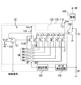
- FIG. 1 is a circuit diagram illustrating a schematic configuration of the driving apparatus according to the first embodiment.
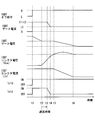
- FIG. 2 is a timing chart showing driving by the driving device.
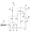
- FIG. 3 is a circuit diagram showing a detailed configuration of the switch circuit.
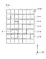
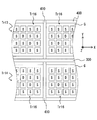
- FIG. 4 is a top view showing a layout of the NMOS transistor.
- FIG. 5 is an enlarged view of the region V shown in FIG.
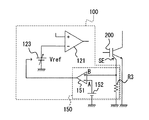
- FIG. 6 is a circuit diagram illustrating a schematic configuration of the drive device according to the first modification.
- FIG. 7 is a circuit diagram illustrating a schematic configuration of the driving apparatus according to the second embodiment.
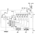
- FIG. 8 is a circuit diagram illustrating a schematic configuration of the driving apparatus according to the third embodiment.
- FIG. 9 is a circuit diagram illustrating a schematic configuration of a drive device according to the second modification.
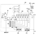
- FIG. 10 is a circuit diagram illustrating a schematic configuration of a drive device according to the third modification.
- the driving device 100 controls driving of an insulated gate bipolar transistor (IGBT) 200 as a power switching element that drives a load 500.
- IGBT insulated gate bipolar transistor
- the driving device 100 includes an on-side circuit 110, an off-side circuit 120, a dV / dt detection circuit 130, and a delay circuit 140.
- the on-side circuit 110 and the off-side circuit 120 are connected in series between the power supply and GND, and the gate of the IGBT 200 is connected to the middle point.
- the on-side circuit 110 is composed of a PMOS transistor, and when the PMOS transistor is in an on state, the power supply voltage Vcc is applied to the gate of the IGBT 200. As a result, the IGBT 200 is turned on, a current flows between the collector and the emitter of the IGBT 200, and power is supplied to the load 500.
- the off-side circuit 120 has a plurality of NMOS transistors (Tr10 to Tr15, Tr20). These NMOS transistors are composed of main MOS transistors (Tr10 to Tr15) as output transistors, and a sense MOS transistor Tr20 that defines the drain current of the main MOS transistor. In this embodiment, six main MOS transistors (Tr10 to Tr15) constitute a current mirror with respect to the sense MOS transistor Tr20. Specifically, the gates of the main MOS transistors (Tr10 to Tr15) are common to the gate of the sense MOS transistor Tr20, and the sources are commonly connected to GND. The drains of the main MOS transistors (Tr10 to Tr15) are connected to the gate of the IGBT 200.
- a drain current flows through each main MOS transistor (Tr10 to Tr15) at the same current ratio as the size ratio of the sense MOS transistor Tr20. That is, in the present embodiment, there are six current paths for the current injected into the gate of the IGBT 200.
- the size is an aspect ratio (W / L) between the channel width W and the channel length L in the MOS transistor.
- the off-side circuit 120 includes an operational amplifier 121 for controlling the drain current of the sense MOS transistor Tr20, a reference resistor 122 for defining the output of the operational amplifier 121, and a reference potential at one input terminal of the operational amplifier 121. And a reference power supply 123 for providing Vref.
- the operational amplifier 121 applies a voltage to the gate of the sense MOS transistor Tr20 so that a constant current is injected into the gate of the IGBT 200. To do.
- the reference resistor 122 is a shunt resistor and defines the current value of the drain current of the sense MOS transistor Tr20. As a result, the current value of the current injected into the gate of the IGBT 200 is defined.
- the current injected into the gate of the IGBT 200 is the sum of drain currents flowing through the main MOS transistors (Tr10 to Tr15). Since the main MOS transistors (Tr10 to Tr15) form a current mirror together with the sense MOS transistor Tr20, the current injected into the gate of the IGBT 200 depends on the drain current of the sense MOS transistor Tr20.
- the operational amplifier 121 when a signal indicating that the IGBT 200 is to be turned off is input, the operational amplifier 121 is driven and a gate voltage is applied to the sense MOS transistor Tr20.
- the drain current at this time is defined by the resistance value R of the reference resistor 122.
- the current value is feedback controlled by adjusting the output of the operational amplifier 121 so that the intermediate potential between the reference resistor 122 and the sense MOS transistor Tr20 approaches the reference potential Vref.
- the sense current control circuit SC corresponds to a circuit configured by the operational amplifier 121, the reference resistor 122, and the reference power source 123.
- the off-side circuit 120 has switch circuits (SW1 to SW5) for switching the current value of the current injected into the gate of the IGBT 200, that is, the drive capability.
- the switch circuits (SW1 to SW5) are connected to the gates of five main MOS transistors (Tr11 to Tr15) among the six main MOS transistors (Tr10 to Tr15), respectively.
- the switch circuit SW1 is enabled and the other switch circuits (SW2 to SW5) are disabled, the gate charge of the IGBT 200 is extracted by the current defined by the main MOS transistors Tr10 and Tr11. That is, the drive capability of the off-side circuit 120 can be controlled depending on which switch circuit is effective among the switch circuits (SW1 to SW5).
- the five switch circuits (SW1 to SW5) are equivalent to each other, and are hereinafter collectively referred to as a symbol SW except when individual switch circuits are described. A detailed circuit configuration of the switch circuit SW in the present embodiment will be described later.
- the dV / dt detection circuit 130 in the driving device 100 is a circuit that detects a time change dV / dt of the collector voltage Vce of the IGBT 200.
- the dV / dt detection circuit 130 is connected in series between the collector of the IGBT 200 and GND, and is connected to an intermediate point between the capacitor C1 and the resistor R1 that form a differentiator.
- a signal indicating that the IGBT 200 is turned off is input to the operational amplifier 121, the gate charge of the IGBT 200 is extracted and the collector voltage Vce rises, so dV / dt takes a non-zero value.
- the dV / dt detection circuit 130 detects this and outputs a message to that effect to the delay circuit 140.
- the delay circuit 140 is a circuit that operates the switch circuit SW with a predetermined delay time from the time when dV / dt starts to rise.
- which switch circuit SW is to be operated may be determined in advance or may be determined according to the value of dV / dt or the like.
- a control signal indicating that the IGBT 200 is to be turned off is input to the operational amplifier 121.
- the operational amplifier 121 is driven and current is injected into the gate of the IGBT 200.
- the switch circuit SW at time t1 is assumed that SW1 is valid (ON) and SW2 to SW5 are invalid (OFF). That is, the current injected into the gate is the total value I1 + I2 of the drain current I1 of the main MOS transistor Tr10 and the drain current I2 of the main MOS transistor Tr11.
- the gate voltage decreases. Then, at time t2, when the gate voltage decreases to a predetermined potential (mirror voltage) and a certain time elapses, the collector voltage Vce starts to increase. That is, at time t2, dV / dt takes a positive value from the state where dV / dt is almost zero. The dV / dt detection circuit 130 detects this and outputs a message to that effect to the delay circuit 140.
- the switch circuit SW1 is turned off, so that the main MOS transistor Tr11 is turned off.
- the main MOS transistor Tr11 is not turned off instantaneously, but takes a falling time defined for the element and is turned off (time t4). For this reason, the current injected into the gate changes from I1 + I2 to I1 from time t3 to time t4. In this period, the change dV / dt of the collector voltage Vce of the IGBT 200 gradually decreases.
- the main MOS transistor Tr11 is turned off, and the gate current of the IGBT 200 is switched from I1 + I2 to I1.
- the drive capability of the off-side circuit 120 in other words, the discharge rate of the gate charge, is smaller at the time t4 than at the time t3. Therefore, dV / dt immediately after time t4 is smaller than dV / dt immediately before time t3. As a result, overshoot of the collector voltage Vce is suppressed, and the effect of reducing the surge voltage can be exhibited. Thereafter, at time t6, the collector voltage Vce converges to a steady value, and the off operation of the IGBT 200 ends.
- the timing for starting the main MOS transistor Tr11 to be turned off (time t3) is set to be earlier than the time t5 when the time t4 when the main MOS transistor Tr11 is completely turned off reaches a steady value of the assumed collector voltage Vce. It is preferred that
- the main MOS transistor Tr11 may be turned on again to improve the drive capability of the off-side circuit 120, thereby ensuring that the IGBT 200 is reliably turned off.
- the switch circuit SW includes a main circuit 125 and a constant current circuit 126 that supplies a constant current I3 to the main circuit 125.
- the main circuit 125 is responsible for energizing and interrupting current between the input terminal IN and the output terminal OUT based on a signal from the delay circuit 140.
- the main circuit 125 has a MOS transistor Tr30 that is turned on and off by a signal from the delay circuit 140.
- the constant current circuit 126 includes two NPN transistors Q1 and Q2 that are connected in parallel with the MOS transistor Tr30 and constitute a current mirror so as to mirror the current I3 input from the constant current circuit 126. Yes.
- the MOS transistor Tr40 that conducts and cuts off the current between the input terminal IN and the output terminal OUT based on the current injected into the gate is provided.
- the input terminal IN shown in FIG. 3 is connected to the output terminal of the operational amplifier 121, and the output terminal OUT is connected to the gates of the main MOS transistors (Tr11 to Tr15).
- the operation of the main circuit 125 will be described.
- the switch circuit SW When the switch circuit SW is turned on, a signal for turning on the MOS transistor Tr30 is input from the delay circuit.
- the current I3 supplied from the constant current circuit 126 flows as the drain current of the MOS transistor Tr30, and no current flows through the NPN transistors Q1 and Q2 forming the current mirror. That is, the current I4 shown in FIG. 3 does not flow. Therefore, the current I5 from the current source P1 is injected into the gate of the MOS transistor Tr40 and turned on, and the input terminal IN and the output terminal OUT are energized. That is, the switch circuit SW is turned on.
- the resistor R1 inserted between the current source P1 and GND is a resistor for defining the gate voltage in the steady state of the MOS transistor Tr40.
- a pull-down resistor R2 is inserted between the output terminal OUT and GND in order to ensure that the switch circuit SW is turned off.
- the constant current circuit 126 described above is a circuit for supplying a constant current I3 to the main circuit 125. Since the constant current circuit 126 can employ a generally known circuit for supplying a constant current, a detailed description of the circuit is omitted.
- the layout of the sense MOS transistor Tr20 and the main MOS transistors (Tr10 to Tr15) will be described with reference to FIG. 4 and FIG.
- the X direction, the Y direction orthogonal to the X direction, and the Z direction orthogonal to the XY plane defined by the X direction and the Y direction are defined.
- These NMOS transistors are formed on the surface layer of the semiconductor substrate 300 along the XY plane.
- the NMOS transistors constituting the main MOS transistors Tr10 to Tr15 and the sense MOS transistor Tr20 are formed with unit MOS transistors Tr16 arranged in a 7 ⁇ 7 lattice along the X and Y directions. LDMOS (lateral diffusion MOS).
- the 49 unit MOS transistors Tr16 one corresponds to the sense MOS transistor Tr20 and the remaining 48 correspond to the main MOS transistors (Tr10 to Tr15).
- the main MOS transistors (Tr10 to Tr15) are each composed of eight unit MOS transistors Tr16.
- FIG. 5 is an enlarged view of the region V shown in FIG.
- each unit MOS transistor Tr16 has a plurality of source regions S and drain regions D formed in a lattice pattern.
- one cell is formed by 4 ⁇ 4.
- a gate region G is formed so as to surround the source region S and the drain region D forming one cell.
- the gate region G and the source region S and drain region D forming a 4 ⁇ 4 lattice constitute one unit MOS transistor Tr16.
- the sense MOS transistor Tr20 and the main MOS transistors (Tr10 to Tr15) are all composed of the same unit MOS transistor Tr16.
- the unit MOS transistor Tr16 has a trench 400 for electrically isolating elements from each other.
- the trench 400 is formed from the surface layer of the semiconductor substrate 300 along the Z direction, and surrounds each unit MOS transistor Tr16.
- the trench 400 is formed in a bowl shape so as to surround the gate region G in each unit MOS transistor Tr16.
- one side 410 of the trench 400 formed between adjacent NMOS transistors, for example, unit MOS transistors Tr16 adjacent in the X direction shares both trenches 400.
- one side of the trench 400 between the unit MOS transistors Tr16 adjacent in the Y direction is not shared.
- each unit MOS transistor Tr16 in this embodiment has the shape and area of the source region S, the shape and area of the drain region D, except for the partial arrangement of the source region S and the drain region D, The shape and area of the gate region G are formed equivalent to each other. That is, the unit MOS transistor Tr16 constituting the main MOS transistors (Tr10 to Tr15) and the sense MOS transistor Tr20 are all formed to have the same channel length L and channel width W.
- a plurality of main MOS transistors (Tr10 to Tr15) constituting a sense MOS transistor Tr20 and a current mirror are formed, and the validity / invalidity of these is controlled by on / off control of the switch circuit SW. Therefore, the output current can be switched by switching the number of valid main MOS transistors (Tr10 to Tr15).
- the drain current of the sense MOS transistor Tr20 that defines the drain current of the main MOS transistors (Tr10 to Tr15) by the current mirror is defined by the reference potential Vref and the resistance value R of the reference resistor 122. Therefore, the output current can be controlled with high accuracy regardless of the power supply voltage Vcc that supplies power to the driving apparatus 100 according to the present disclosure and the current value of the output current of the off-side circuit 120. Further, since the drain current of the sense MOS transistor Tr20 is constant regardless of whether the switch circuit SW is turned on or off, the output current is controlled with high accuracy regardless of the number of main MOS transistors (Tr10 to Tr15) that are enabled. be able to.
- the drain current of the sense MOS transistor Tr20 is defined by the reference potential Vref and the resistance value R of the standard resistor 122, the drain-source voltage Vds of the sense MOS transistor Tr20 is sufficiently higher than the threshold voltage (so-called Vth). Can keep big.
- the resistance value R of the reference resistor 122 can be reduced, the same semiconductor substrate as the main MOS transistors (Tr10 to Tr15) and the sense MOS transistor Tr20 can be obtained without separately preparing a resistor serving as the reference resistor 122 as a discrete component. 300 can be integrated.
- a trench 400 that isolates the unit MOS transistors Tr16 constituting each NMOS transistor (Tr20, Tr10 to Tr15) from each other is partially shared between adjacent unit MOS transistors Tr16. Yes.
- one side 410 of the bowl-shaped trench 400 is shared by the unit MOS transistors Tr16 adjacent in the X direction. Therefore, the layout area in the X direction can be reduced as compared with the configuration in which the trench 400 is not shared.
- the main MOS transistors (Tr10 to Tr15) and the sense MOS transistor Tr20 are formed so that the unit MOS transistor Tr16 and the channel width W are the same. Since all the unit MOS transistors Tr16 are equivalently formed, the drive device 100 can be easily manufactured, and the characteristics of the drain current with respect to the voltage applied to the gate can be made uniform. Further, as shown in FIG. 4, since the unit MOS transistors Tr16 can be arranged in a lattice pattern, the ratio of the NMOS transistors to the surface layer area of the semiconductor substrate 300 can be reduced. That is, the layout area can be reduced.
- the drive device 100 includes a current detection unit 150 as shown in FIG.
- the reference power supply 123 has a variable reference potential Vref.
- the on-side circuit 110, the NMOS transistors (Tr10 to Tr15, Tr20), the switch circuit SW, the reference resistor 122, the dV / dt detection circuit 130, and the delay circuit 140 are not shown.
- the current detection unit 150 is a circuit that detects the collector current of the IGBT 200 and protects it from overcurrent.
- the current detection unit 150 includes a comparator 151, a voltage source 152 that applies a threshold voltage to one input terminal of the comparator 151, and a resistor R3 that converts the collector current of the IGBT 200 into a voltage. .
- the voltage source 152 is connected to one input terminal A of the comparator 151.
- the other input terminal B is connected to an intermediate point between the resistor R3 connected between the sense emitter terminal SE of the IGBT 200 and GND. That is, the voltage corresponding to the current flowing from the sense emitter terminal SE of the IGBT 200 toward the GND and the resistance value of the resistor R3 is applied to the input terminal B of the comparator 151.
- the voltage applied to the input terminal B is proportional to the current flowing from the sense emitter terminal SE toward GND. That is, this voltage becomes higher as the collector current of the IGBT 200 increases.
- the comparator 151 applies a reference potential to the reference power supply 123 when the voltage corresponding to the current flowing through the sense emitter terminal SE exceeds the voltage of the voltage source 152, that is, when the collector current exceeds a predetermined threshold. Control to increase Vref.
- the on-side circuit 110 has a plurality of PMOS transistors (Tr50 to Tr55, Tr60). These PMOS transistors are composed of a main MOS transistor (Tr50 to Tr55) as an output transistor and a sense MOS transistor Tr60 that defines the drain current of the main MOS transistor.
- a main MOS transistor Tr50 to Tr55
- a sense MOS transistor Tr60 that defines the drain current of the main MOS transistor.
- six main MOS transistors (Tr50 to Tr55) form a current mirror with respect to the sense MOS transistor Tr60.
- the gates of the main MOS transistors (Tr50 to Tr55) are common to the gate of the sense MOS transistor Tr60, and the drains are commonly connected to the power supply Vcc.
- the source of each main MOS transistor (Tr50 to Tr55) is connected to the gate of the IGBT 200.
- the on-side circuit 110 includes an operational amplifier 111 for controlling the drain current of the sense MOS transistor Tr60, a reference resistor 112 for defining the output of the operational amplifier 111, and a reference potential at one input terminal of the operational amplifier 111. And a reference power supply 113 for providing Vref.
- the operational amplifier 111 applies a voltage to the gate of the sense MOS transistor Tr60 so that a constant current is supplied to the gate of the IGBT 200. To do.
- the on-side circuit 110 has switch circuits (SW6 to SW10) for switching the current value of the current supplied to the gate of the IGBT 200, that is, the drive capability.
- the switch circuits (SW6 to SW10) are connected to the gates of five main MOS transistors (Tr51 to Tr55) among the six main MOS transistors (Tr50 to Tr55), respectively.
- These switch circuits (SW6 to SW10) are equivalent to the switch circuit SW described in the first embodiment, and the circuit configuration shown in FIG. 3 can be adopted as the circuit configuration.
- the main MOS transistors (Tr50 to Tr55), the sense MOS transistor Tr60, the operational amplifier 111, the reference resistor 112, the reference power supply 113, and the switch circuits (SW6 to SW10), which are components in the present embodiment, are respectively the first embodiment.
- the elements corresponding to the main MOS transistors (Tr10 to Tr15), the sense MOS transistor Tr20, the operational amplifier 121, the reference resistor 122, the reference power supply 123, and the switch circuits (SW1 to SW5) Therefore, the operation and effect of each component are the same as those in the first embodiment and its modification. That is, the output current of the on-side circuit 110 can be controlled with high accuracy, and the switching speed can be increased as compared with the case where it is controlled by the reference current.
- reference potential Vref in the present embodiment does not necessarily coincide with the reference potential Vref in the first embodiment.
- the sense current control circuit SC is not limited to a circuit constituted by the operational amplifiers 111 and 121, the reference resistors 112 and 122, and the reference power sources 113 and 123.
- the sense current control circuit SC in each of the above-described embodiments is configured to be feedback-controlled so as to have a current value defined by the resistance value R of the reference resistors 112 and 122 and the reference potential Vref of the reference power sources 113 and 123. It was. On the other hand, the sense current control circuit SC in the present embodiment is configured not to perform feedback control.
- the sense current control circuit SC of the off-side circuit 160 in this embodiment includes an operational amplifier 161 having an output terminal connected to the gate of the sense MOS transistor Tr20, and one of the operational amplifiers 161. And a reference power supply 162 that applies a predetermined voltage to the input terminal.
- the output of the operational amplifier 161 is negatively fed back to the other input terminal, and a voltage defined by the reference power supply 162 is applied to the sense MOS transistor Tr20.
- the output current can be switched by switching the number of valid main MOS transistors (Tr10 to Tr15).
- the sense current control circuit SC as in the first and second embodiments is adopted as compared with the present embodiment, the drain current of the sense MOS transistor Tr20 can be maintained with high accuracy, but the load 500 does not require high accuracy. In the case of driving, the number of parts and the manufacturing cost can be reduced by employing the sense current control circuit SC according to the present embodiment.
- the Vds adjustment circuit 163 in this modification is, for example, a Wilson type current mirror circuit, and two current paths are connected to the drains of the sense MOS transistor Tr20 and the main MOS transistors (Tr10 to Tr15), respectively.
- the drain-source voltage Vds of each NMOS transistor is adjusted to be constant, the drain current of each NMOS transistor can be controlled with higher accuracy.
- the sense current control circuit SC of the off-side circuit 160 in this embodiment includes an operational amplifier 161 and a current source P2 that supplies a predetermined current to one input terminal of the operational amplifier 161, as shown in FIG. And a temperature sensitive element 164 connected in parallel with the current source P2 with respect to the operational amplifier 161.
- the temperature sensing element 164 in this modification is, for example, a temperature sensing diode.
- the threshold voltage and charge mobility of each NMOS transistor generally have negative temperature characteristics, and the voltage drop amount (Vf) of the temperature sensitive diode also has negative temperature characteristics. Therefore, as shown in FIG.
- the current source P2 and the temperature sensitive diode are connected to the non-inverting input terminal of the operational amplifier 161, and the output of the operational amplifier 161 is negatively fed back to the inverting input terminal.
- the gate voltages of the sense MOS transistor Tr20 and the main MOS transistors can be lowered as the temperature of the drive device 100 increases. That is, the change in the gate voltage of the IGBT 200 due to the temperature can be suppressed.
- the temperature sensitive element 164 is not limited to a temperature sensitive diode.
- the IGBT 200 is illustrated as the power switching element, but is not limited to this example.
- the present disclosure can be applied to a power MOS transistor or the like as a power switching element.
- circuit configuration as shown in FIG. 3 is illustrated as the switch circuit SW, it is not limited to this. That is, it is only necessary to control the current supply and interruption between the input terminal IN and the output terminal OUT based on the output of the delay circuit 140.
- the driving device 100 has one sense MOS transistor Tr20
- a plurality of sense MOS transistors Tr20 may be formed.
- a plurality of main MOS transistors corresponding to each sense MOS transistor are formed.
- the number of main MOS transistors is not limited to the above example.
- modification 2 and modification 3 describes variations of the sense current control circuit SC with respect to the off-side circuit, but can also be applied to the on-side circuit 110.
Landscapes
- Engineering & Computer Science (AREA)
- Physics & Mathematics (AREA)
- Electromagnetism (AREA)
- General Physics & Mathematics (AREA)
- Radar, Positioning & Navigation (AREA)
- Automation & Control Theory (AREA)
- Power Conversion In General (AREA)
- Electronic Switches (AREA)
- Insulated Gate Type Field-Effect Transistor (AREA)
- Metal-Oxide And Bipolar Metal-Oxide Semiconductor Integrated Circuits (AREA)
Abstract
パワースイッチング素子(200)を制御する駆動装置は、前記パワースイッチング素子のオン動作を行うオン側回路(110)と、オフ動作を行うオフ側回路(120)と、を備える。前記オンまたはオフ側回路は、複数メインMOSトランジスタ(Tr10~Tr15,Tr50~Tr55)と、前記メインMOSトランジスタのドレイン電流を規定するセンスMOSトランジスタ(Tr20,Tr60)と、前記センスMOSトランジスタのドレイン電流を一定に制御するセンス電流制御回路(SC)と、前記メインMOSトランジスタのゲートに接続され、前記メインMOSトランジスタのオンオフを制御することで前記パワースイッチング素子のゲート電流を切り替えるスイッチ回路(SW)を有する。
Description
本開示は、2014年3月27日に出願された日本出願番号2014-66595号と、2014年10月28日に出願された日本出願番号2014-219348号に基づくもので、ここにその記載内容を援用する。
本開示は、パワースイッチング素子のオンオフ動作を行う駆動装置に関する。
インバータやコンバータ等の半導体電力変換装置を構成するパワースイッチング素子について、スイッチング動作時のサージ電圧とスイッチング損失とのトレードオフを解消する技術として、ゲート電圧あるいはゲート電流を動的に制御するアクティブゲートコントロール(AGC)が用いられている。
例えば、パワースイッチング素子として絶縁ゲートバイポーラトランジスタ(IGBT)を用いる場合、ターンオフ時のコレクタ-エミッタ間電圧(以降、コレクタ電圧Vceという)の時間変化dV/dtをフィードバックして、IGBTのゲート電荷の放電速度を制御する。具体的には、特許文献1において、IGBTのゲートに注入するゲート電流の電流量を切り替えることによって、ゲート電荷の放電速度を、放電の途中で切り替える技術が提案されている。しかしながら、特許文献1の技術は、切り替え段数に対応する数のゲートオフ回路が必要となるため、回路規模、すなわちレイアウト面積が大きくなってしまう。
一方、特許文献2では、広い出力電流を有する、換言すれば、出力電流を幅広く切り替えることのできる半導体装置において、レイアウト面積を抑えることのできる回路が提案されている。具体的には、この半導体装置は、出力電流をリファレンス電流のカレントミラーによって生成する。そして、カレントミラーを多段とすることによって、出力電流の広いダイナミックレンジを実現している。
しかしながら、特許文献2の技術は、出力トランジスタをオンするためのゲートへの電流供給をリファレンス電流によって行うため、カレントミラーを構成する出力トランジスタの段数が増加するほどリファレンス電流が変化してしまう。すなわち、出力トランジスタをオンするごとに出力電流が変動してしまう。
また、特許文献2のような回路構成では、一般に、リファレンス電流をできるだけ小さくすることが望ましいが、カレントミラーを構成する出力トランジスタのゲートへの電荷の注入速度がリファレンス電流に依存するため、リファレンス電流が小さいと出力トランジスタがオンするまでの時間が長くなってしまう。つまり、特許文献2の技術をパワースイッチング素子のオフ用回路に適用する場合、パワースイッチング素子をオフする旨の指示を受けてから出力トランジスタがオンするまでの応答速度が確保できない虞がある。
本開示は、上記問題点を鑑みてなされたものであり、ゲート電流を高精度で制御しつつ、ゲート電流の切り替え速度の高速化することを目的とする。
本開示のある態様において、パワースイッチング素子のオンオフを制御する駆動装置は、前記パワースイッチング素子のオン動作を行うオン側回路と、前記パワースイッチング素子のオフ動作を行うオフ側回路と、を備える。前記オン側回路および前記オフ側回路の少なくとも一方の回路は、出力トランジスタとしての複数のメインMOSトランジスタと、前記メインMOSトランジスタとゲートが共通し、前記メインMOSトランジスタに対してカレントミラーを構成することによって、前記メインMOSトランジスタのドレイン電流を規定するセンスMOSトランジスタと、前記センスMOSトランジスタのドレイン電流を一定に制御するセンス電流制御回路と、を有する。さらに、前記オン側回路および前記オフ側回路の少なくとも一方の回路は、前記メインMOSトランジスタのゲートに接続され、前記メインMOSトランジスタのオンオフを制御することにより前記パワースイッチング素子におけるゲート電流を切り替えるスイッチ回路を有する。
これによれば、センスMOSトランジスタとカレントミラーを構成するメインMOSトランジスタが複数形成され、これらの有効/無効がスイッチ回路のオンオフ制御によって制御されている。このため、有効とされるメインMOSトランジスタの数を切り替えることによって、出力電流を切り替えることができる。
また、カレントミラーによってメインMOSトランジスタのドレイン電流を規定するセンスMOSトランジスタのドレイン電流が、参照電位と基準抵抗の抵抗値によって規定される。このため、本発明に係る駆動装置に電力を供給する電源電圧や、オフ側回路の出力電流の電流値に依らず、出力電流を高精度に制御することができる。さらに、センスMOSトランジスタのドレイン電流はスイッチ回路のオンオフに依らず一定であるから、有効とされるメインMOSトランジスタの数に依らず、出力電流を高精度に制御することができる。
また、出力トランジスタとしてのメインMOSトランジスタを駆動させるためのゲートへの電圧印加がオペアンプの出力によって制御されるため、リファレンス電流によって制御される場合に較べて、スイッチング速度を高速化することができる。
本開示についての上記目的およびその他の目的、特徴や利点は、添付の図面を参照しながら下記の詳細な記述により、より明確になる。その図面は、
図1は、第1実施形態に係る駆動装置の概略構成を示す回路図である。
図2は、駆動装置による駆動を示すタイミングチャートである。
図3は、スイッチ回路の詳細な構成を示す回路図である。
図4は、NMOSトランジスタのレイアウトを示す上面図である。
図5は、図4に示す領域Vの拡大図である。
図6は、変形例1に係る駆動装置の概略構成を示す回路図である。
図7は、第2実施形態に係る駆動装置の概略構成を示す回路図である。
図8は、第3実施形態に係る駆動装置の概略構成を示す回路図である。
図9は、変形例2に係る駆動装置の概略構成を示す回路図である。
図10は、変形例3に係る駆動装置の概略構成を示す回路図である。
(第1実施形態)
最初に、図1を参照して、本実施形態に係る駆動装置について説明する。
最初に、図1を参照して、本実施形態に係る駆動装置について説明する。
図1に示すように、この駆動装置100は、負荷500を駆動するパワースイッチング素子としての絶縁ゲートバイポーラトランジスタ(IGBT)200の駆動を制御するものである。
この駆動装置100は、オン側回路110と、オフ側回路120と、dV/dt検出回路130と、遅延回路140と、を備えている。
オン側回路110およびオフ側回路120は電源とGNDとの間で直列に接続され、その中間点にIGBT200のゲートが接続されている。オン側回路110は、PMOSトランジスタにより構成され、このPMOSトランジスタがオン状態のときにはIGBT200のゲートに電源電圧Vccが印加される。これによりIGBT200がオン状態になり、IGBT200のコレクタ-エミッタ間に電流が流れ、負荷500に電力が供給される。
オフ側回路120は、複数のNMOSトランジスタ(Tr10~Tr15,Tr20)を有している。これらNMOSトランジスタは、出力トランジスタとしてのメインMOSトランジスタ(Tr10~Tr15)と、メインMOSトランジスタのドレイン電流を規定するセンスMOSトランジスタTr20とから構成されている。本実施形態では、6つのメインMOSトランジスタ(Tr10~Tr15)が、センスMOSトランジスタTr20に対してカレントミラーを構成するようになっている。具体的には、各メインMOSトランジスタ(Tr10~Tr15)のゲートはセンスMOSトランジスタTr20のゲートと共通とされ、ソースが共通してGNDに接続されている。各メインMOSトランジスタ(Tr10~Tr15)のドレインはIGBT200のゲート接続されている。
このような構成では、各メインMOSトランジスタ(Tr10~Tr15)には、それぞれ、センスMOSトランジスタTr20のサイズ比と同一の電流比でドレイン電流が流れる。つまり、本実施形態では、IGBT200のゲートに注入する電流の電流経路が6つ存在している。なお、サイズとはMOSトランジスタにおけるチャネル幅Wとチャネル長Lのアスペクト比(W/L)である。
また、オフ側回路120は、センスMOSトランジスタTr20のドレイン電流を制御するためのオペアンプ121と、該オペアンプ121の出力を規定するための基準抵抗122と、該オペアンプ121の一つの入力端子に参照電位Vrefを与える参照電源123と、を有している。オペアンプ121は、図示しないマイコンなどからIGBT200をオフさせることを示す制御信号が入力されると、センスMOSトランジスタTr20のゲートに電圧を印加することで、IGBT200のゲートに定電流が注入されるようにする。
基準抵抗122は、シャント抵抗であり、センスMOSトランジスタTr20のドレイン電流の電流値を規定する。ひいては、IGBT200のゲートに注入される電流の電流値を規定する。IGBT200のゲートに注入される電流は、メインMOSトランジスタ(Tr10~Tr15)に流れるドレイン電流の合計である。そして、メインMOSトランジスタ(Tr10~Tr15)はセンスMOSトランジスタTr20とともにカレントミラーを構成しているので、IGBT200のゲートに注入される電流はセンスMOSトランジスタTr20のドレイン電流に依存する。
このような構成では、IGBT200をオフさせることを示す信号が入力されると、オペアンプ121が駆動されてセンスMOSトランジスタTr20にゲート電圧が印加される。このときのドレイン電流は基準抵抗122の抵抗値Rにより規定される。そして、その電流値は、基準抵抗122とセンスMOSトランジスタTr20との間の中間電位が、参照電位Vrefに近づくように、オペアンプ121の出力が調整されることによりフィードバック制御される。これにより、センスMOSトランジスタTr20のドレイン電流が高精度に一定の値(=(Vcc-Vref)/R)に制御される。よって、IGBT200のゲートに注入される電流も、高精度に一定電流とされる。なお、本実施形態において、センス電流制御回路SCは、オペアンプ121と基準抵抗122および参照電源123とにより構成される回路に相当する。
さらに、オフ側回路120は、IGBT200のゲートに注入される電流の電流値、すなわちドライブ能力を切り替えるためのスイッチ回路(SW1~SW5)を有している。このスイッチ回路(SW1~SW5)は、6つのメインMOSトランジスタ(Tr10~Tr15)のうち5つのメインMOSトランジスタ(Tr11~Tr15)のゲートにそれぞれ接続されている。例えば、スイッチ回路SW1が有効とされ、その他のスイッチ回路(SW2~SW5)が無効の状態であれば、IGBT200のゲート電荷は、メインMOSトランジスタTr10およびTr11により規定される電流により引き抜かれる。つまり、スイッチ回路(SW1~SW5)のうち、どのスイッチ回路が有効となっているかによってオフ側回路120のドライブ能力を制御することができる。なお、5つのスイッチ回路(SW1~SW5)は互いに等価であり、以降、個々のスイッチ回路について述べる場合を除き、符号SWと総称する。本実施形態におけるスイッチ回路SWの詳しい回路構成は追って説明する。
駆動装置100におけるdV/dt検出回路130は、IGBT200のコレクタ電圧Vceの時間変化dV/dtを検出する回路である。具体的には、dV/dt検出回路130は、IGBT200のコレクタとGNDとの間に直列接続されて微分器を構成するコンデンサC1と抵抗器R1の中間点に接続されている。オペアンプ121にIGBT200をオフさせることを示す信号が入力されると、IGBT200のゲート電荷が引き抜かれてコレクタ電圧Vceが上昇するため、dV/dtがゼロでない値をとる。dV/dt検出回路130はこれを検出し、その旨を遅延回路140に出力する。
遅延回路140は、dV/dtが上昇を開始した時点から所定の遅延時間だけ遅れてスイッチ回路SWを動作させる回路である。5つのスイッチ回路(SW1~SW5)のうち、どのスイッチ回路SWを動作させるかについては、予め決めておくこともできるし、dV/dtの値等に応じて決定されてもよい。
次に、本実施形態に係る駆動装置100における、IGBT200のゲート電荷の放電期間中の放電速度を切り替える駆動について、図2を参照して説明する。
時刻t1において、オペアンプ121にIGBT200をオフさせることを示す制御信号が入力される。これにより、図2に示すように、オペアンプ121が駆動してIGBT200のゲートに電流が注入される。この説明において、時刻t1におけるスイッチ回路SWは、SW1が有効(オン)とされ、SW2~SW5は無効(オフ)であるとする。つまり、ゲートに注入される電流は、メインMOSトランジスタTr10のドレイン電流I1と、メインMOSトランジスタTr11のドレイン電流I2との合計値I1+I2である。
IGBT200のゲートに電流が注入されて電荷の引き抜きが行われ始めると、ゲート電圧は低下していく。そして、時刻t2において、ゲート電圧が所定の電位(ミラー電圧)まで低下し一定時間が経過すると、コレクタ電圧Vceが上昇を始める。すなわち、時刻t2の時点で、dV/dtがほぼゼロの状態から、dV/dtが正の値をとる。dV/dt検出回路130はこれを検出して、その旨を遅延回路140に対して出力する。
そして、遅延回路140により予め規定された遅延時間後の時刻t3において、スイッチ回路SW1がオフされることによって、メインMOSトランジスタTr11のオフ動作が開始される。メインMOSトランジスタTr11は瞬時にオフされるのではなく、素子に規定された立ち下がり時間を要してオフ(時刻t4)に至る。このため、ゲートに注入される電流は、時刻t3から時刻t4に至る間に、I1+I2からI1へ変化する。そして、この期間において、IGBT200のコレクタ電圧Vceの変化dV/dtは、徐々に小さくなっていく。時刻t4に至ると、メインMOSトランジスタTr11はオフ状態となり、IGBT200のゲート電流は、I1+I2からI1に切り替わる。
このため、オフ側回路120のドライブ能力、換言すればゲート電荷の放電速度、は、時刻t3の時点に較べて時刻t4の時点のほうが小さくなる。したがって、時刻t3直前のdV/dtに比べて、時刻t4直後のdV/dtは小さくなる。その結果、コレクタ電圧Vceのオーバーシュートが抑制され、サージ電圧を低減する効果を発揮することができる。その後、時刻t6において、コレクタ電圧Vceが定常値に収束してIGBT200のオフ動作は終了する。
なお、メインMOSトランジスタTr11のオフ開始のタイミング(時刻t3)は、メインMOSトランジスタTr11が完全にオフになる時刻t4が、想定されるコレクタ電圧Vceの定常値に至る時刻t5よりも早い時期に設定されることが好ましい。
また、時刻t6以降において、再びメインMOSトランジスタTr11をオンしてオフ側回路120のドライブ能力を向上させることによって、IGBT200の確実なオフを保証するように構成しても良い。
次に、図3を参照して、本実施形態におけるスイッチ回路SWの具体的な構成について説明する。なお、図3に示す回路は、各スイッチ回路(SW1~SW5)いずれも同一の構成である。
スイッチ回路SWは、主回路125と、主回路125に一定の電流I3を供給する定電流回路126とを有している。
主回路125は、遅延回路140からの信号に基づいて入力端子INと出力端子OUTの間における電流の通電および遮断を担っている。主回路125は、図3に示すように、遅延回路140からの信号によりオンオフ動作するMOSトランジスタTr30を有している。また、定電流回路126に対して、MOSトランジスタTr30と並列に接続され、定電流回路126から入力される電流I3をミラーするようにカレントミラーを構成する2つのNPNトランジスタQ1,Q2を有している。また、ゲートに注入される電流に基づいて入力端子INと出力端子OUTの間における電流の通電および遮断を行うMOSトランジスタTr40を有している。さらに、スイッチ回路SWをオン状態とする場合にMOSトランジスタTr40のゲートに電流を注入する電流源P1を有している。なお、本実施形態では、図3に示す入力端子INがオペアンプ121の出力端子に接続されており、出力端子OUTがメインMOSトランジスタ(Tr11~Tr15)のゲートに接続されている。
主回路125の動作について説明する。スイッチ回路SWをオン状態とする場合、遅延回路からMOSトランジスタTr30をオン状態とする旨の信号が入力される。この状態では、定電流回路126から供給される電流I3は、MOSトランジスタTr30のドレイン電流として流れ、カレントミラーを成すNPNトランジスタQ1,Q2に電流が流れない。すなわち、図3に示す電流I4は流れない。このため、電流源P1からの電流I5がMOSトランジスタTr40のゲートに注入されてオンとなり、入力端子INと出力端子OUTの間が通電される。すなわち、スイッチ回路SWがオン状態となる。なお、電流源P1とGNDとの間に挿入された抵抗器R1は、MOSトランジスタTr40の定常状態におけるゲート電圧を規定するための抵抗である。
一方、スイッチ回路SWをオフ状態とする場合、遅延回路からMOSトランジスタTr30をオフ状態とする旨の信号が入力される。この状態では、MOSトランジスタTr30のドレイン電流は流れず、定電流回路126から主回路125に入力される電流I3は、NPNトランジスタQ1,Q2によりミラーされて図3に示す電流I4が流れる。この電流I4は、電流源P1による電流I5およびMOSトランジスタTr40のゲート電荷を引き抜くように流れるため、MOSトランジスタTr40がオフする。よって、入力端子INと出力端子OUTの間の電流が遮断されてスイッチ回路SWがオフ状態となる。なお、スイッチ回路SWがオフすると、対応するメインMOSトランジスタのゲートがハイインピーダンスとなる。本実施形態におけるスイッチ回路SWは、スイッチ回路SWのオフ動作を確実にするため、出力端子OUTとGNDとの間にプルダウン抵抗器R2が挿入されている。
前述の定電流回路126は、主回路125に一定の電流I3を供給するための回路である。この定電流回路126は、一定の電流を与えるための一般的に知られた回路を採用することができるため、回路の詳細な説明を割愛する。
次に、図4および図5を参照して、センスMOSトランジスタTr20およびメインMOSトランジスタ(Tr10~Tr15)のレイアウトについて説明する。便宜上、図4に示すように、X方向と、X方向に直交するY方向と、X方向とY方向により規定されるXY平面に直交するZ方向を定義する。これらNMOSトランジスタは半導体基板300の表層において、XY平面に沿って形成されている。
図4に示すように、メインMOSトランジスタTr10~Tr15およびセンスMOSトランジスタTr20を構成するNMOSトランジスタは、X方向およびY方向に沿って、単位MOSトランジスタTr16が7×7の格子状に並んで形成されたLDMOS(横方向拡散MOS)である。本実施形態では、49個の単位MOSトランジスタTr16のうち、1個がセンスMOSトランジスタTr20に相当し、残りの48個がメインMOSトランジスタ(Tr10~Tr15)に相当する。なお、図4に示すように、メインMOSトランジスタ(Tr10~Tr15)は、それぞれ8個の単位MOSトランジスタTr16から構成されている。
これらNMOSトランジスタのレイアウトについてより詳しく説明する。図5は図4に示す領域Vを拡大した図である。図5に示すように、各単位MOSトランジスタTr16には、それぞれ複数のソース領域Sとドレイン領域Dが格子状に形成されている。本実施形態では、4×4で1つのセルを形成している。そして、1つのセルを形成するソース領域Sおよびドレイン領域Dを取り囲むように、ゲート領域Gが形成されている。このゲート領域Gと、4×4の格子を成すソース領域Sおよびドレイン領域Dと、により一つの単位MOSトランジスタTr16を構成している。なお、センスMOSトランジスタTr20、メインMOSトランジスタ(Tr10~Tr15)は、すべて同一の単位MOSトランジスタTr16から構成されている。
さらに、図5に示すように、単位MOSトランジスタTr16は、互いに電気的に素子分離するためのトレンチ400を有している。トレンチ400は、半導体基板300の表層からZ方向に沿って形成されるとともに、各単位MOSトランジスタTr16をそれぞれ取り囲んで形成されている。換言すれば、トレンチ400は、各単位MOSトランジスタTr16におけるゲート領域Gを取り囲むように、枡状に形成されている。そして、本実施形態では、隣り合うNMOSトランジスタ、例えば、X方向において隣り合う単位MOSトランジスタTr16の間に形成されたトレンチ400の一辺410が、双方のトレンチ400を共有している。なお、本実施形態では、Y方向において隣り合う単位MOSトランジスタTr16の間のトレンチ400の一辺は共有されていない。
また、図5に示すように、本実施形態における各単位MOSトランジスタTr16は、ソース領域Sやドレイン領域Dの一部配置を除き、ソース領域Sの形状および面積、ドレイン領域Dの形状および面積、ゲート領域Gの形状および面積が、互いに等価に形成されている。すなわち、メインMOSトランジスタ(Tr10~Tr15)およびセンスMOSトランジスタTr20を構成する単位MOSトランジスタTr16は、チャネル長Lとチャネル幅Wがすべて同一に形成されている。
次に、本実施形態に係る駆動装置100の作用効果について説明する。
図1に示すように、センスMOSトランジスタTr20とカレントミラーを構成するメインMOSトランジスタ(Tr10~Tr15)が複数形成され、これらの有効/無効がスイッチ回路SWのオンオフ制御によって制御されている。このため、有効とされるメインMOSトランジスタ(Tr10~Tr15)の数を切り替えることによって、出力電流を切り替えることができる。
また、カレントミラーによってメインMOSトランジスタ(Tr10~Tr15)のドレイン電流を規定するセンスMOSトランジスタTr20のドレイン電流が、参照電位Vrefと基準抵抗122の抵抗値Rによって規定される。このため、本開示に係る駆動装置100に電力を供給する電源電圧Vccや、オフ側回路120の出力電流の電流値に依らず、出力電流を高精度に制御することができる。さらに、センスMOSトランジスタTr20のドレイン電流は、スイッチ回路SWのオンオフに依らず一定であるから、有効とされるメインMOSトランジスタ(Tr10~Tr15)の数に依らず、出力電流を高精度に制御することができる。
また、出力トランジスタとしてのメインMOSトランジスタ(Tr10~Tr15)を駆動させるためのゲートへの電圧印加がオペアンプ121の出力によって制御されるため、リファレンス電流によって制御される場合に較べて、スイッチング速度を高速化することができる。
さらには、センスMOSトランジスタTr20のドレイン電流が、参照電位Vrefと基準抵抗122の抵抗値Rによって規定されるため、センスMOSトランジスタTr20のドレイン-ソース間電圧Vdsを閾値電圧(いわゆるVth)よりも十分大きく保つことができる。これにより、基準抵抗122の抵抗値Rを小さくできるから、基準抵抗122となる抵抗器をディスクリート部品として別途用意することなく、メインMOSトランジスタ(Tr10~Tr15)やセンスMOSトランジスタTr20と同一の半導体基板300上に集積化することができる。
さらに、図5に示すように、各NMOSトランジスタ(Tr20,Tr10~Tr15)を構成する単位MOSトランジスタTr16を互いに素子分離するトレンチ400が、隣り合う単位MOSトランジスタTr16の間で一部共有化されている。本実施形態においては、X方向に隣り合う単位MOSトランジスタTr16において、枡状のトレンチ400の一辺410が共有化されている。したがって、トレンチ400が共有化されない構成に較べて、X方向のレイアウト面積を小さくすることができる。
また、図5に示すように、メインMOSトランジスタ(Tr10~Tr15)およびセンスMOSトランジスタTr20は、それらを構成する単位MOSトランジスタTr16チャネル長Lとチャネル幅Wがすべて同一に形成されている。各単位MOSトランジスタTr16がすべて等価に形成されているから、駆動装置100の製造が容易になり、ゲートに印加される電圧に対するドレイン電流の特性も均一化することができる。また、図4に示すように、単位MOSトランジスタTr16を格子状に配置することができるため、半導体基板300の表層面積に対するNMOSトランジスタの占める割合を小さくすることができる。すなわち、レイアウト面積を小さくすることができる。
(変形例1)
上記した実施形態における構成に加えて、本変形例では、図6に示すように、駆動装置100が電流検出部150を備えている。また、参照電源123は参照電位Vrefが可変になっている。なお、図6では、オン側回路110、各NMOSトランジスタ(Tr10~Tr15,Tr20)、スイッチ回路SW、基準抵抗122、dV/dt検出回路130および遅延回路140の図示を省略している。
上記した実施形態における構成に加えて、本変形例では、図6に示すように、駆動装置100が電流検出部150を備えている。また、参照電源123は参照電位Vrefが可変になっている。なお、図6では、オン側回路110、各NMOSトランジスタ(Tr10~Tr15,Tr20)、スイッチ回路SW、基準抵抗122、dV/dt検出回路130および遅延回路140の図示を省略している。
電流検出部150はIGBT200のコレクタ電流を検出して、過電流から保護する回路である。この電流検出部150は、コンパレータ151と、コンパレータ151の一方の入力端子に閾値となる電圧を与える電圧源152と、IGBT200のコレクタ電流を電圧に変換するための抵抗器R3とを有している。
前述のように、コンパレータ151の一方の入力端子Aには電圧源152が接続されている。そして、他方の入力端子Bは、IGBT200のセンスエミッタ端子SEとGNDとの間に接続された抵抗器R3との中間点に接続されている。すなわち、コンパレータ151における入力端子Bには、IGBT200のセンスエミッタ端子SEからGNDに向かって流れる電流と抵抗器R3の抵抗値に対応した電圧が印加されている。入力端子Bに印加される電圧は、センスエミッタ端子SEからGNDに向かって流れる電流に比例する。つまり、この電圧はIGBT200のコレクタ電流が大きくなるほど高電圧となる。
コンパレータ151は、センスエミッタ端子SEを流れる電流に対応した電圧が、電圧源152の電圧を超えた場合、すなわち、コレクタ電流が所定の閾値を超えた場合に、参照電源123に対して、参照電位Vrefを大きくするように制御する。
これによれば、IGBT200に過度のコレクタ電流(過電流)が流れている場合に、参照電位Vrefが大きくされることによって、センスMOSトランジスタTr20のドレイン電流が小さくなる。このため、オフ側回路120のドライブ能力が抑制され、IGBT200を緩やかにオフすることができる。したがって、過電流発生時において、サージ電圧を抑制することができ、IGBT200を保護することができる。
(第2実施形態)
上記した実施形態では、オフ側回路120において、IGBT200の温度に基づく制御を可能にした例について示したが、これはオン側回路110についても適用することができる。
上記した実施形態では、オフ側回路120において、IGBT200の温度に基づく制御を可能にした例について示したが、これはオン側回路110についても適用することができる。
具体的には、図7に示すように、オン側回路110は、複数のPMOSトランジスタ(Tr50~Tr55,Tr60)を有している。これらPMOSトランジスタは、出力トランジスタとしてのメインMOSトランジスタ(Tr50~Tr55)と、メインMOSトランジスタのドレイン電流を規定するセンスMOSトランジスタTr60とから構成されている。本実施形態では、6つのメインMOSトランジスタ(Tr50~Tr55)が、センスMOSトランジスタTr60に対してカレントミラーを構成するようになっている。具体的には、各メインMOSトランジスタ(Tr50~Tr55)のゲートはセンスMOSトランジスタTr60のゲートと共通とされ、ドレインが共通して電源Vccに接続されている。各メインMOSトランジスタ(Tr50~Tr55)のソースはIGBT200のゲート接続されている。
また、オン側回路110は、センスMOSトランジスタTr60のドレイン電流を制御するためのオペアンプ111と、該オペアンプ111の出力を規定するための基準抵抗112と、該オペアンプ111の一つの入力端子に参照電位Vrefを与える参照電源113と、を有している。オペアンプ111は、図示しないマイコンなどからIGBT200をオンさせることを示す制御信号が入力されると、センスMOSトランジスタTr60のゲートに電圧を印加することで、IGBT200のゲートへ定電流が供給されるようにする。
さらに、オン側回路110は、IGBT200のゲートへ供給される電流の電流値、すなわちドライブ能力を切り替えるためのスイッチ回路(SW6~SW10)を有している。このスイッチ回路(SW6~SW10)は、6つのメインMOSトランジスタ(Tr50~Tr55)のうち5つのメインMOSトランジスタ(Tr51~Tr55)のゲートにそれぞれ接続されている。これらスイッチ回路(SW6~SW10)は、第1実施形態に記載のスイッチ回路SWと等価であり、その回路構成は、図3に示す回路構成を採用することができる。
本実施形態における構成要素である、メインMOSトランジスタ(Tr50~Tr55)、センスMOSトランジスタTr60、オペアンプ111、基準抵抗112、参照電源113、およびスイッチ回路(SW6~SW10)は、それぞれ、第1実施形態におけるメインMOSトランジスタ(Tr10~Tr15)、センスMOSトランジスタTr20、オペアンプ121、基準抵抗122、参照電源123、およびスイッチ回路(SW1~SW5)に相当する要素である。よって、各構成要素の動作および作用効果は、第1実施形態およびその変形例に準じるものである。すなわち、オン側回路110の出力電流を高精度に制御することができ、また、リファレンス電流によって制御される場合に較べて、スイッチング速度を高速化することができる。
なお、本実施形態における参照電位Vrefは、第1実施形態における参照電位Vrefと必ずしも一致している必要はない。
(第3実施形態)
センス電流制御回路SCは、オペアンプ111,121と基準抵抗112,122および参照電源113,123とにより構成される回路に限定されない。
センス電流制御回路SCは、オペアンプ111,121と基準抵抗112,122および参照電源113,123とにより構成される回路に限定されない。
上記した各実施形態におけるセンス電流制御回路SCでは、基準抵抗112,122の抵抗値Rと参照電源113,123の参照電位Vrefとによって規定される電流値になるようにフィードバック制御されるよう構成されていた。これに対して、本実施形態におけるセンス電流制御回路SCは、フィードバック制御を行わない構成となっている。
具体的には、本実施形態におけるオフ側回路160のセンス電流制御回路SCは、図8に示すように、センスMOSトランジスタTr20のゲートに出力端子が接続されたオペアンプ161と、オペアンプ161の一方の入力端子に所定の電圧を印加する参照電源162と、を有している。他方の入力端子には、オペアンプ161の出力が負帰還されており、参照電源162により規定される電圧がセンスMOSトランジスタTr20に印加されるようになっている。このような構成であっても、有効とされるメインMOSトランジスタ(Tr10~Tr15)の数を切り替えることによって、出力電流を切り替えることができる。なお、本実施形態に較べて第1および第2実施形態のようなセンス電流制御回路SCを採用したほうが、センスMOSトランジスタTr20のドレイン電流を高精度に維持できるが、高精度を要しない負荷500を駆動する場合には本実施形態に係るセンス電流制御回路SCを採用することによって部品点数や製造コストを低減することができる。
(変形例2)
第3実施形態におけるセンス電流制御回路SCの、センスMOSトランジスタTr20およびメインMOSトランジスタ(Tr10~Tr15)へ供給するゲート電流を高精度に制御するために、図9に示すように、Vds調整回路163を採用することができる。
第3実施形態におけるセンス電流制御回路SCの、センスMOSトランジスタTr20およびメインMOSトランジスタ(Tr10~Tr15)へ供給するゲート電流を高精度に制御するために、図9に示すように、Vds調整回路163を採用することができる。
本変形例におけるVds調整回路163は、例えばウィルソン型のカレントミラー回路であり、2つの電流経路がセンスMOSトランジスタTr20およびメインMOSトランジスタ(Tr10~Tr15)のドレインにそれぞれ接続されている。これにより、各NMOSトランジスタのドレイン-ソース間電圧Vdsが一定に調整されるため、より精度良く各NMOSトランジスタのドレイン電流を制御することができる。
(変形例3)
センスMOSトランジスタTr20およびメインMOSトランジスタ(Tr10~Tr15)の閾値電圧や電荷の移動度は一般に温度特性を有しているので、温度の変化とともにIGBT200のゲート電圧が変化する虞がある。本変形例では、これを抑制するため、センス電流制御回路SCとして、第3実施形態および変形例2に示した参照電源162に適切な温度特性を持たせた構成を採用している。
センスMOSトランジスタTr20およびメインMOSトランジスタ(Tr10~Tr15)の閾値電圧や電荷の移動度は一般に温度特性を有しているので、温度の変化とともにIGBT200のゲート電圧が変化する虞がある。本変形例では、これを抑制するため、センス電流制御回路SCとして、第3実施形態および変形例2に示した参照電源162に適切な温度特性を持たせた構成を採用している。
具体的には、本実施形態におけるオフ側回路160のセンス電流制御回路SCは、図10に示すように、オペアンプ161と、所定の電流をオペアンプ161の一方の入力端子に供給する電流源P2と、オペアンプ161に対して電流源P2と並列接続された感温素子164と、を有している。本変形例における感温素子164は、例えば感温ダイオードである。各NMOSトランジスタの閾値電圧や電荷の移動度は一般に負の温度特性を有し、また、感温ダイオードの電圧降下量(Vf)も負の温度特性を有する。このため、図10に示すように、オペアンプ161の非反転入力端子に電流源P2および感温ダイオードを接続し、反転入力端子にオペアンプ161の出力を負帰還させる。これによって、駆動装置100の温度上昇に合わせて、センスMOSトランジスタTr20およびメインMOSトランジスタ(Tr10~Tr15)のゲート電圧を低下させることができる。すなわち、温度によるIGBT200のゲート電圧の変化を抑制することができる。なお、感温素子164としては、感温ダイオードに限定されるものではない。
(その他の実施形態)
以上、本開示の好ましい実施形態について説明したが、本開示は上記した実施形態になんら制限されることなく、本開示の主旨を逸脱しない範囲において、種々変形して実施することが可能である。
以上、本開示の好ましい実施形態について説明したが、本開示は上記した実施形態になんら制限されることなく、本開示の主旨を逸脱しない範囲において、種々変形して実施することが可能である。
上記した実施形態および変形例では、パワースイッチング素子としてIGBT200を例示したが、この例に限定されない。例えば、パワースイッチング素子として、パワーMOSトランジスタ等についても本開示を適用することができる。
また、スイッチ回路SWとして、図3に示すような回路構成を例示したが、これに限定されない。すなわち、遅延回路140の出力に基づいて、入力端子INと出力端子OUT間における電流の通電および遮断を制御できればよい。
また、上記した実施形態および変形例では、駆動装置100が、一つのセンスMOSトランジスタTr20を有する例について示したが、センスMOSトランジスタTr20は複数形成されてもよい。この場合、各センスMOSトランジスタそれぞれに対応したメインMOSトランジスタが複数形成される。また、メインMOSトランジスタの数についても上記例に限定されない。
さらに、上記した実施形態および変形例では、センスMOSトランジスタTr20を構成する単位MOSトランジスタTr16が1個である例を示したがこの数についても限定されない。また、メインMOSトランジスタ(Tr10~Tr15)を構成する単位MOSトランジスタTr16が8個である例を示したが、この数についても限定されるものではない。
上記した第3実施形態、変形例2および変形例3の説明は、オフ側回路に対してセンス電流制御回路SCのバリエーションを記載したものであるが、オン側回路110に適用することもできる。
本開示は、実施例に準拠して記述されたが、本開示は当該実施例や構造に限定されるものではないと理解される。本開示は、様々な変形例や均等範囲内の変形をも包含する。加えて、様々な組み合わせや形態、さらには、それらに一要素のみ、それ以上、あるいはそれ以下、を含む他の組み合わせや形態をも、本開示の範疇や思想範囲に入るものである。
Claims (6)
- パワースイッチング素子(200)のオンオフを制御する駆動装置であって、
前記パワースイッチング素子のオン動作を行うオン側回路(110)と、
前記パワースイッチング素子のオフ動作を行うオフ側回路(120)と、を備え、
前記オン側回路および前記オフ側回路の少なくとも一方の回路は、
出力トランジスタとしての複数のメインMOSトランジスタ(Tr10~Tr15,Tr50~Tr55)と、
前記メインMOSトランジスタとゲートが共通し、前記メインMOSトランジスタに対してカレントミラーを構成することによって、前記メインMOSトランジスタのドレイン電流を規定するセンスMOSトランジスタ(Tr20,Tr60)と、
前記センスMOSトランジスタのドレイン電流を一定に制御するセンス電流制御回路(SC)と、を有し、
さらに、前記オン側回路および前記オフ側回路の少なくとも一方の回路は、
前記メインMOSトランジスタのゲートに接続され、前記メインMOSトランジスタのオンオフを制御することにより前記パワースイッチング素子におけるゲート電流を切り替えるスイッチ回路(SW)を有する駆動装置。 - 前記センス電流制御回路は、
参照電位(Vref)を発生させる参照電源(113,123)と、
前記センスMOSトランジスタに直列接続された基準抵抗(112,122)と、
前記基準抵抗と前記センスMOSトランジスタとの間の電位が前記参照電位に近づくように前記センスMOSトランジスタのゲートに出力を発生させるオペアンプ(111,121)と、を有して、
前記センス電流制御回路は、前記センスMOSトランジスタのドレイン電流として前記基準抵抗の抵抗値と前記参照電位とによって決まる電流を流す請求項1に記載の駆動装置。 - 前記センス電流制御回路は、
前記センスMOSトランジスタのゲートに出力を発生させるオペアンプ(161)と、
所定の電流を前記オペアンプの一方の入力端子に供給する電流源(P2)と、
前記オペアンプに対して前記電流源と並列接続された感温素子(164)と、を有して、
温度に依存する前記感温素子の電圧降下に基づいて、前記センスMOSトランジスタのドレイン電流を変化させるように構成される請求項1に記載の駆動装置。 - 前記メインMOSトランジスタおよび前記センスMOSトランジスタを構成する単位MOSトランジスタ(Tr16)は、チャネル長(L)およびチャネル幅(W)がすべて同一に構成される請求項1~3のいずれか1項に記載の駆動装置。
- 前記メインMOSトランジスタおよび前記センスMOSトランジスタを構成する単位MOSトランジスタは、隣接する素子との間にトレンチ(400)を有して素子分離されるLDMOSにより構成され、
前記トレンチは、隣り合う素子において互いに共有される請求項4に記載の駆動装置。 - 前記パワースイッチング素子のコレクタ電流を検出する電流検出部(150)をさらに備え、
前記電流検出部は、前記パワースイッチング素子のコレクタ電流が所定の閾値を超える場合において、前記パワースイッチング素子のコレクタ電流が所定の閾値を超えない場合に較べて前記センスMOSトランジスタのゲート電圧を小さく設定する請求項1~5のいずれか1項に記載の駆動装置。
Priority Applications (2)
| Application Number | Priority Date | Filing Date | Title |
|---|---|---|---|
| US15/117,512 US9800237B2 (en) | 2014-03-27 | 2015-03-12 | Drive device |
| CN201580015851.6A CN106134049B (zh) | 2014-03-27 | 2015-03-12 | 驱动装置 |
Applications Claiming Priority (4)
| Application Number | Priority Date | Filing Date | Title |
|---|---|---|---|
| JP2014-066595 | 2014-03-27 | ||
| JP2014066595 | 2014-03-27 | ||
| JP2014-219348 | 2014-10-28 | ||
| JP2014219348A JP6237570B2 (ja) | 2014-03-27 | 2014-10-28 | 駆動装置 |
Publications (1)
| Publication Number | Publication Date |
|---|---|
| WO2015146038A1 true WO2015146038A1 (ja) | 2015-10-01 |
Family
ID=54194592
Family Applications (1)
| Application Number | Title | Priority Date | Filing Date |
|---|---|---|---|
| PCT/JP2015/001363 Ceased WO2015146038A1 (ja) | 2014-03-27 | 2015-03-12 | 駆動装置 |
Country Status (4)
| Country | Link |
|---|---|
| US (1) | US9800237B2 (ja) |
| JP (1) | JP6237570B2 (ja) |
| CN (1) | CN106134049B (ja) |
| WO (1) | WO2015146038A1 (ja) |
Cited By (3)
| Publication number | Priority date | Publication date | Assignee | Title |
|---|---|---|---|---|
| CN106329916A (zh) * | 2016-08-29 | 2017-01-11 | 杰华特微电子(杭州)有限公司 | 开关管的驱动方法及电路及电源系统 |
| US9900000B2 (en) | 2014-03-27 | 2018-02-20 | Denso Corporation | Drive device |
| CN109417386A (zh) * | 2016-07-04 | 2019-03-01 | 三菱电机株式会社 | 驱动电路以及使用该驱动电路的功率模块 |
Families Citing this family (19)
| Publication number | Priority date | Publication date | Assignee | Title |
|---|---|---|---|---|
| JP6296082B2 (ja) * | 2016-03-09 | 2018-03-20 | トヨタ自動車株式会社 | 駆動装置 |
| WO2017208735A1 (ja) * | 2016-06-03 | 2017-12-07 | 富士電機株式会社 | 半導体装置 |
| JP2018037723A (ja) * | 2016-08-29 | 2018-03-08 | 公立大学法人首都大学東京 | ゲート駆動装置 |
| US10110220B1 (en) * | 2017-06-08 | 2018-10-23 | Texas Instruments Incorporated | Auxiliary MOSFETs for switchable coupling to a power MOSFET |
| JP6917793B2 (ja) * | 2017-06-13 | 2021-08-11 | ローム株式会社 | 電流調節回路、それを用いた電源管理回路 |
| JP6890480B2 (ja) * | 2017-06-19 | 2021-06-18 | 日立Astemo株式会社 | 半導体装置 |
| JP7196048B2 (ja) * | 2019-10-23 | 2022-12-26 | 株式会社東芝 | サージ制御回路及び電力変換器 |
| JP2021096089A (ja) | 2019-12-13 | 2021-06-24 | 株式会社東芝 | 電圧変化率検出回路、半導体装置及び電力変換器 |
| JP7356340B2 (ja) * | 2019-12-25 | 2023-10-04 | 株式会社タムラ製作所 | ゲート駆動回路 |
| EP3849083A1 (en) * | 2020-01-07 | 2021-07-14 | Hamilton Sundstrand Corporation | Gate driver |
| JP2022143030A (ja) * | 2021-03-17 | 2022-10-03 | 富士電機株式会社 | 駆動回路、半導体装置 |
| JP2023002041A (ja) * | 2021-06-22 | 2023-01-10 | 日清紡マイクロデバイス株式会社 | スイッチング電源装置 |
| JP7195386B1 (ja) | 2021-07-27 | 2022-12-23 | 三菱電機株式会社 | 電力変換装置 |
| JPWO2023181660A1 (ja) * | 2022-03-25 | 2023-09-28 | ||
| CN114978137B (zh) * | 2022-05-05 | 2025-04-01 | 北京市科通电子继电器总厂有限公司 | 一种功率开关器件的驱动控制电路、系统和集成电路 |
| JP7111273B1 (ja) | 2022-05-16 | 2022-08-02 | 富士電機株式会社 | ゲート駆動装置 |
| CN116360536A (zh) * | 2023-02-27 | 2023-06-30 | 上海艾为电子技术股份有限公司 | 基准电压电路及芯片 |
| CN120898536A (zh) * | 2023-03-22 | 2025-11-04 | 三菱电机株式会社 | 半导体装置及半导体装置的制造方法 |
| US20250191529A1 (en) * | 2023-06-08 | 2025-06-12 | Chipone Technology (Beijing) Co., Ltd. | Power supply circuit, chip and display screen |
Citations (5)
| Publication number | Priority date | Publication date | Assignee | Title |
|---|---|---|---|---|
| JPH11299221A (ja) * | 1998-04-10 | 1999-10-29 | Fuji Electric Co Ltd | パワー素子のドライブ回路 |
| JP2010283973A (ja) * | 2009-06-04 | 2010-12-16 | Denso Corp | パワースイッチング素子の駆動装置 |
| US20110316507A1 (en) * | 2010-06-28 | 2011-12-29 | Wuxi Vimicro Corporation | Multiple-input comparator and power converter |
| JP4954290B2 (ja) * | 2007-10-02 | 2012-06-13 | 三菱電機株式会社 | ゲート駆動回路 |
| JP2014054019A (ja) * | 2012-09-05 | 2014-03-20 | Denso Corp | スイッチング素子の駆動回路 |
Family Cites Families (13)
| Publication number | Priority date | Publication date | Assignee | Title |
|---|---|---|---|---|
| US5293077A (en) | 1988-02-29 | 1994-03-08 | Hitachi, Ltd. | Power switching circuit |
| JP3885563B2 (ja) | 2001-11-16 | 2007-02-21 | 日産自動車株式会社 | パワー半導体駆動回路 |
| JP2006020098A (ja) | 2004-07-02 | 2006-01-19 | Toshiba Corp | 半導体装置 |
| JP4876440B2 (ja) | 2005-06-03 | 2012-02-15 | 株式会社デンソー | 半導体装置 |
| ATE535999T1 (de) | 2006-02-21 | 2011-12-15 | Nxp Bv | Exponentieller digital-analog-umsetzer |
| JP4755197B2 (ja) * | 2006-05-29 | 2011-08-24 | 株式会社オートネットワーク技術研究所 | 電力供給制御装置 |
| JP2012098220A (ja) * | 2010-11-04 | 2012-05-24 | Advantest Corp | 試験装置 |
| JP5195896B2 (ja) * | 2010-12-27 | 2013-05-15 | 株式会社デンソー | 電気負荷駆動装置 |
| JP5938852B2 (ja) * | 2011-05-25 | 2016-06-22 | 富士電機株式会社 | 電圧制御型スイッチング素子のゲート駆動回路 |
| CN103188177B (zh) * | 2011-12-30 | 2016-09-07 | 意法半导体研发(上海)有限公司 | Lin驱动器中的电磁发射的有效减小的方法 |
| US9094005B2 (en) * | 2013-07-30 | 2015-07-28 | Denso Corporation | Semiconductor element module and gate drive circuit |
| JP6349897B2 (ja) | 2014-04-11 | 2018-07-04 | 株式会社デンソー | 駆動回路のタイミング調整方法及び駆動回路のタイミング調整回路 |
| JP6398300B2 (ja) | 2014-05-09 | 2018-10-03 | 株式会社デンソー | 車載キャリブレーション装置 |
-
2014
- 2014-10-28 JP JP2014219348A patent/JP6237570B2/ja not_active Expired - Fee Related
-
2015
- 2015-03-12 WO PCT/JP2015/001363 patent/WO2015146038A1/ja not_active Ceased
- 2015-03-12 CN CN201580015851.6A patent/CN106134049B/zh not_active Expired - Fee Related
- 2015-03-12 US US15/117,512 patent/US9800237B2/en not_active Expired - Fee Related
Patent Citations (5)
| Publication number | Priority date | Publication date | Assignee | Title |
|---|---|---|---|---|
| JPH11299221A (ja) * | 1998-04-10 | 1999-10-29 | Fuji Electric Co Ltd | パワー素子のドライブ回路 |
| JP4954290B2 (ja) * | 2007-10-02 | 2012-06-13 | 三菱電機株式会社 | ゲート駆動回路 |
| JP2010283973A (ja) * | 2009-06-04 | 2010-12-16 | Denso Corp | パワースイッチング素子の駆動装置 |
| US20110316507A1 (en) * | 2010-06-28 | 2011-12-29 | Wuxi Vimicro Corporation | Multiple-input comparator and power converter |
| JP2014054019A (ja) * | 2012-09-05 | 2014-03-20 | Denso Corp | スイッチング素子の駆動回路 |
Cited By (4)
| Publication number | Priority date | Publication date | Assignee | Title |
|---|---|---|---|---|
| US9900000B2 (en) | 2014-03-27 | 2018-02-20 | Denso Corporation | Drive device |
| CN109417386A (zh) * | 2016-07-04 | 2019-03-01 | 三菱电机株式会社 | 驱动电路以及使用该驱动电路的功率模块 |
| CN109417386B (zh) * | 2016-07-04 | 2022-10-04 | 三菱电机株式会社 | 驱动电路以及使用该驱动电路的功率模块 |
| CN106329916A (zh) * | 2016-08-29 | 2017-01-11 | 杰华特微电子(杭州)有限公司 | 开关管的驱动方法及电路及电源系统 |
Also Published As
| Publication number | Publication date |
|---|---|
| JP2015195700A (ja) | 2015-11-05 |
| JP6237570B2 (ja) | 2017-11-29 |
| US20160352316A1 (en) | 2016-12-01 |
| CN106134049B (zh) | 2018-10-30 |
| US9800237B2 (en) | 2017-10-24 |
| CN106134049A (zh) | 2016-11-16 |
Similar Documents
| Publication | Publication Date | Title |
|---|---|---|
| JP6237570B2 (ja) | 駆動装置 | |
| JP6187428B2 (ja) | 駆動装置 | |
| JP6349855B2 (ja) | 駆動装置 | |
| KR101970112B1 (ko) | 파워 스위칭 장치 | |
| US7548403B2 (en) | Overcurrent detection circuit | |
| JP5627512B2 (ja) | パワーモジュール | |
| CN102893525B (zh) | 对电压驱动型元件进行驱动的驱动装置 | |
| US9666505B1 (en) | Power MOS transistor die with temperature sensing function and integrated circuit | |
| TW201942698A (zh) | 電壓調整器 | |
| KR101783484B1 (ko) | 가변 저항 회로를 구비한 반도체 집적 회로 | |
| KR20150107628A (ko) | 전압 검출 회로 | |
| JP2020030179A (ja) | 電流検出回路 | |
| KR101215830B1 (ko) | Ldmos 소자를 이용한 스위치 회로 | |
| JP2010011012A (ja) | クランプ機能付コンパレータ | |
| KR20180018759A (ko) | 스타트-업 회로들 | |
| JP4665452B2 (ja) | 温度検知回路、および温度検知回路を備えたパワー半導体装置 | |
| JP2005295360A (ja) | 電流検出回路およびそれを用いた半導体集積装置、レギュレータ装置 | |
| JP2022013339A (ja) | 短絡判定装置、および、スイッチ装置 | |
| JP2007315836A (ja) | 過熱検知装置 | |
| JP5726349B2 (ja) | パワーモジュール | |
| JP2008235974A (ja) | 定電流制御回路および該回路を備えた半導体集積回路 | |
| US20080068072A1 (en) | Ratioed Feedback Body Voltage Bias Generator | |
| KR100622350B1 (ko) | 저전압 디지털 cmos 공정에서 다른 문턱 전압을 가지는 mosfet들을 이용한 적층형 cmos 커런트 미러 | |
| JPH05152521A (ja) | 定電流回路 | |
| JP2007310566A (ja) | オペアンプ回路 |
Legal Events
| Date | Code | Title | Description |
|---|---|---|---|
| 121 | Ep: the epo has been informed by wipo that ep was designated in this application |
Ref document number: 15769450 Country of ref document: EP Kind code of ref document: A1 |
|
| WWE | Wipo information: entry into national phase |
Ref document number: 15117512 Country of ref document: US |
|
| NENP | Non-entry into the national phase |
Ref country code: DE |
|
| 122 | Ep: pct application non-entry in european phase |
Ref document number: 15769450 Country of ref document: EP Kind code of ref document: A1 |