WO2015141492A1 - Antenne à puce - Google Patents
Antenne à puce Download PDFInfo
- Publication number
- WO2015141492A1 WO2015141492A1 PCT/JP2015/056602 JP2015056602W WO2015141492A1 WO 2015141492 A1 WO2015141492 A1 WO 2015141492A1 JP 2015056602 W JP2015056602 W JP 2015056602W WO 2015141492 A1 WO2015141492 A1 WO 2015141492A1
- Authority
- WO
- WIPO (PCT)
- Prior art keywords
- antenna
- top wall
- chip antenna
- chip
- pattern
- Prior art date
Links
Images


Classifications
-
- H—ELECTRICITY
- H01—ELECTRIC ELEMENTS
- H01Q—ANTENNAS, i.e. RADIO AERIALS
- H01Q1/00—Details of, or arrangements associated with, antennas
- H01Q1/12—Supports; Mounting means
- H01Q1/22—Supports; Mounting means by structural association with other equipment or articles
- H01Q1/2283—Supports; Mounting means by structural association with other equipment or articles mounted in or on the surface of a semiconductor substrate as a chip-type antenna or integrated with other components into an IC package
-
- H—ELECTRICITY
- H01—ELECTRIC ELEMENTS
- H01Q—ANTENNAS, i.e. RADIO AERIALS
- H01Q1/00—Details of, or arrangements associated with, antennas
- H01Q1/12—Supports; Mounting means
- H01Q1/22—Supports; Mounting means by structural association with other equipment or articles
- H01Q1/2291—Supports; Mounting means by structural association with other equipment or articles used in bluetooth or WI-FI devices of Wireless Local Area Networks [WLAN]
-
- H—ELECTRICITY
- H01—ELECTRIC ELEMENTS
- H01Q—ANTENNAS, i.e. RADIO AERIALS
- H01Q1/00—Details of, or arrangements associated with, antennas
- H01Q1/36—Structural form of radiating elements, e.g. cone, spiral, umbrella; Particular materials used therewith
- H01Q1/38—Structural form of radiating elements, e.g. cone, spiral, umbrella; Particular materials used therewith formed by a conductive layer on an insulating support
-
- H—ELECTRICITY
- H01—ELECTRIC ELEMENTS
- H01Q—ANTENNAS, i.e. RADIO AERIALS
- H01Q9/00—Electrically-short antennas having dimensions not more than twice the operating wavelength and consisting of conductive active radiating elements
- H01Q9/04—Resonant antennas
- H01Q9/30—Resonant antennas with feed to end of elongated active element, e.g. unipole
- H01Q9/42—Resonant antennas with feed to end of elongated active element, e.g. unipole with folded element, the folded parts being spaced apart a small fraction of the operating wavelength
Definitions
- the present invention relates to a chip antenna incorporated in a wireless communication device having a wireless communication function such as a mobile phone (including a smartphone), a tablet PC, a smart meter (digital watt hour meter), and the like.
- a wireless communication device having a wireless communication function such as a mobile phone (including a smartphone), a tablet PC, a smart meter (digital watt hour meter), and the like.
- a chip-like antenna that can be mounted on the surface of a circuit board is preferably used as an antenna incorporated in this type of wireless communication device.
- This chip antenna includes a chip-shaped base made of a resin having a high dielectric constant and an antenna pattern made of a conductor formed on the surface of the base. For example, a step of forming a conductor film on the surface of the base made of resin A step of forming a mask pattern corresponding to the antenna pattern shape on the conductor film, and a conductive film region exposed from the mask pattern is removed by etching, and then the desired antenna is formed on the substrate by removing the mask pattern. It can be manufactured through a process of forming a pattern.
- Patent Document 1 a chip antenna comprising an antenna pattern formed by bending a conductive plate into a three-dimensional shape, and a base that is injection-molded with resin using the three-dimensional antenna pattern as an insert part.
- a rectangular parallelepiped base may be thinned.
- the substrate since the rigidity of the substrate is greatly reduced only by thinning the substrate, the substrate may be greatly deformed with a temperature change or the like, for example. In this case, it becomes more difficult to hold the antenna pattern on the surface.
- an object of the present invention is to reduce the cost of a chip antenna that can prevent deformation of a base body due to molding shrinkage and temperature change as much as possible, and thereby stably exhibit desired antenna characteristics. There is to provide to.
- the present invention has an antenna pattern in which a conductive plate is bent into a three-dimensional shape and has an antenna part and a terminal part electrically connected to a circuit board, and the antenna pattern is inserted.
- a chip antenna including a base body that is injection-molded with resin as a component, the base body is provided with a rectangular plate-like top wall that holds the antenna portion on the surface, and a short side that is erected along the long side direction of the top wall. One end in the direction is connected to the top wall, and the other end in the short side direction is provided with a rectangular plate-like vertical wall holding the terminal portion.
- the antenna unit is a part that performs at least one of transmission and reception of radio waves.
- the base body is provided with a rectangular plate-like top wall and a rectangular plate-like vertical wall that is erected along the long side direction of the top wall and one end in the short side direction is connected to the top wall.
- each part of the base can be thinned (thinned) to reduce the amount of sink marks caused by molding shrinkage, and the top wall rigidity (bending rigidity) can be increased to increase the length of the top wall. It is possible to prevent as much as possible the warping / bending of the substrate in the direction along. Therefore, the antenna portion of the antenna pattern can be stably held on the surface of the base body (top wall), and desired antenna characteristics can be exhibited.
- the usage-amount of resin can be restrained and cost reduction can be aimed at.
- the base body can take any shape as long as a three-dimensional antenna pattern can be injection molded as an insert part.
- a vertical wall can be provided along the two long sides of the top wall.
- the base body (chip antenna) exhibits a concave shape (reverse concave shape) in an arbitrary cross section in a direction orthogonal to the long side direction, so that the rigidity of the chip antenna can be effectively increased.
- the antenna pattern is provided with a protrusion embedded in the substrate, the holding power of the antenna pattern with respect to the substrate can be increased.
- the above-mentioned protrusion is provided on the antenna portion of the antenna pattern, it is possible to effectively prevent the antenna portion from being peeled off from the base, so that desired antenna characteristics can be stably exhibited. Is preferable.
- the chip antenna having the above-described configuration can be provided with a through-hole that is opened on the top and bottom surfaces of the top wall at a position directly below the antenna portion of the antenna pattern and whose inner wall surface is formed by a base molding die.
- the substrate is injection-molded in a state where the antenna portion of the antenna pattern is appropriately arranged on the surface side of the top wall. Accordingly, the shape accuracy of the top wall (base body) and the position accuracy of the antenna portion with respect to the top wall can be improved, so that desired antenna characteristics can be exhibited.
- At least the surface roughness of the bonding surface of the conductive plate constituting the antenna pattern is Ra 1.6 or more.
- the base molding resin preferably has a high dielectric constant from the viewpoint of securing desired antenna characteristics, and specifically, a resin having a dielectric constant of 4 or more is preferable.
- the resin having a dielectric constant of 4 or higher is not necessarily limited to a base resin having a dielectric constant of 4 or higher, but includes a resin having a dielectric constant of 4 or higher as a whole by blending of fillers.
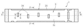
- FIG. 3 is a cross-sectional view of the chip antenna, taken along the line EE shown in FIG.
- FIG. 3 is a cross-sectional view of the chip antenna, taken along the line FF shown in FIG. FIG.
- FIG. 3 is a cross-sectional view of the chip antenna, taken along the line GG shown in FIG.
- FIG. 7 is a process explanatory diagram for manufacturing the chip antenna shown in FIGS. 1 to 6; It is a figure which shows typically the clamping state of the molding die for injection-molding the base
- FIG. 1 is a schematic perspective view of a circuit board 10 on which a chip antenna 1 according to an embodiment of the present invention is mounted.
- a chip antenna 1 shown in FIG. 1 includes an antenna pattern 3 made of a conductive plate, and a base body 2 injection-molded with a resin using the antenna pattern 3 as an insert part.
- the total length of the chip antenna 1 (the dimension in the left-right direction in FIG. 2) varies depending on the frequency (wavelength) of radio waves transmitted and received by the chip antenna 1, but is about 10 to 50 mm, for example.
- the upper direction, the lower direction, the left direction, and the right direction in FIG. 1 are respectively “up”, “down”, “left”, and “right”.
- the usage mode of the chip antenna 1 is not limited.
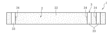
- the antenna pattern 3 is formed by bending a conductive plate into a three-dimensional shape, and as shown in FIGS. 2 to 7, an antenna unit 31 for transmitting and receiving radio waves and a plurality of terminal units 32 (the book) 7 in the embodiment) and a plurality of connection portions 33 for connecting the antenna portion 31 and each terminal portion 32 are integrally provided.
- radio waves are also transmitted and received by the connection unit 33, but the amount of radio waves transmitted and received by the connection unit 33 is negligibly small compared to the amount of radio waves transmitted and received by the antenna unit 31.
- a conductive plate for example, a metal plate such as a copper plate, a steel plate, or a SUS plate, or a plate obtained by plating these metal plates, and the plate thickness can be maintained within a range where a desired three-dimensional shape can be maintained as much as possible.
- the one set thinly for example, 1 mm or less, more preferably 0.5 mm or less
- the surface roughness of the joint surface of the antenna pattern 3 (conductive plate) with the substrate 2 is set to Ra 1.6 or more, preferably 3.2 or more.
- At least one of the plurality (seven) terminal portions 32 of the antenna pattern 3 functions as a power supply terminal electrically connected to the power supply line of the circuit board 10, and at least one of the remaining terminal portions 32.
- One functions as a ground terminal for grounding the antenna pattern 3 to the ground via the circuit board 10.
- the terminal portion 32 other than the power supply terminal and the ground terminal functions as a fixing portion for fixing the chip antenna 1 to the circuit board 10.
- the base 2 is injection-molded with resin using the antenna pattern 3 as an insert part.
- the molding resin for the substrate 2 one having a dielectric constant of 4 or more is selectively used.
- PPS polyphenylene sulfide
- LCP liquid crystal polymer
- PA polyamide
- thermoplastic resins can be used as a base resin, which is mixed with a filler such as ceramics.
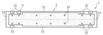
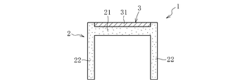
- the base body 2 is erected along a rectangular plate-like top wall 21 holding the antenna portion 31 of the antenna pattern 3 on the surface (upper surface) and two long sides of the top wall 21, and has one end (upper end) in the short side direction. ) Are connected to the top wall 21 and are provided with rectangular plate-like vertical walls 22 and 22 holding the terminal portions 32 of the antenna pattern 3 at the other end (lower end surface) in the short side direction.
- the end walls 23 and 23 are further provided at both ends of the top wall 21 in the long side direction. That is, the base body 2 of the present embodiment has a concave shape (reverse concave shape) in the cross-sectional shape of each part in the long side direction except for both ends in the long side direction.
- the thicknesses of the top wall 21, the pair of vertical walls 22 and the pair of end walls 23, 23 are set to be approximately equal within a range of 0.5 mm to 2.0 mm, for example.
- the three connection parts 33 included in the antenna pattern 3 are held on the surface (left side surface) of the left vertical wall 22, and the four connection parts 33 is held on the surface (right side surface) of the right vertical wall 22.
- the seven terminal portions 32 of the antenna pattern 3 are held on the lower end surface of the left vertical wall 22, and the four terminal portions 32 are on the lower end surface of the right vertical wall 22. It is held (see FIG. 5).
- the antenna pattern 3 has a protrusion 34 embedded in the base 2.
- the antenna portion 31 is provided with five protrusions 34, and each connection portion 33 is provided with one protrusion 34. In this way, the holding force of the antenna pattern 3 with respect to the base 2 can be increased.
- the projecting portion 34 is provided on the antenna portion 31, it is possible to effectively prevent the antenna portion 31 from peeling (raising) from the base body 2 (top wall 21), so that the desired antenna characteristics can be stabilized. This is advantageous in that it can be exhibited.
- the protrusion part 34 provided in the antenna part 31 is the antenna part 31 (more specifically, the part used as the antenna part 31 among the expansion
- This is formed by bending a tongue-like portion formed by forming a slit penetrating the front and back surfaces of the front and back surfaces to the back surface side with the base end as a fulcrum (see FIG. 8).
- the slit is formed in a U-shape, but may be formed in other shapes such as a semicircle. Further, in the present embodiment, as shown in FIG.
- the protruding portion 34 is formed by bending the tongue piece-like portion 90 ° to the back side, but the bending angle of the tongue piece-like portion is arbitrarily set. Is possible.
- one protrusion 34 provided on each connection portion 33 is formed by bending a tongue-like portion formed on a hoop material 40 (deployment pattern 3 ′) as a conductive plate by punching press processing. (See FIG. 9).
- substrate 2 has the several through-hole 25 opened on the front and back both surfaces, as shown in FIG.
- Each through hole 25 is open on both the front and back surfaces of the top wall 21 at a position directly below the antenna portion 31, and the inner wall surface thereof is formed with a molding surface formed by a molding die 50 (see FIG. 10) of the base 2. Is done.
- the chip antenna 1 of this embodiment includes a long conductive plate (hoop material 40), a first step S1 for forming the development pattern 3 ′, a second step S2 for forming the antenna pattern 3, and a base body. 2 is manufactured by sequentially supplying to a third step S3 for injection molding 2 and a fourth step S4 for taking out the chip antenna 1.
- the second step S2 is performed in multiple times (four times).
- a development pattern 3 'in which the three-dimensional antenna pattern 3 is developed on a plane is formed by punching a part of the hoop material 40 with a press mold (not shown).
- the development pattern 3 ′ is connected to the frame 41 of the hoop material 40 via the bridge 42.
- Reference numeral 43 shown in FIG. 9 is a positioning hole of the hoop material 40 with respect to a conveying device (not shown).
- the hoop material 40 is conveyed downward in FIG. 9, and the portion of the hoop material 40 where the development pattern 3 ′ is formed is sequentially applied to the first to fourth stages of the second step S2. Supplied.
- the second step S2 in the first stage, a slit is formed in a portion of the development pattern 3 ′ that becomes the antenna portion 31 of the antenna pattern 3, and thereafter, in the second to fourth stages, the development pattern 3 ′ is sequentially formed. Bending is applied.
- the three-dimensional antenna pattern 3 having the antenna portion 31, the terminal portion 32, and the connection portion 33 integrally formed on the hoop material 40, and the projection portion 34 formed on the antenna portion 31 and the connection portion 33 is formed.
- the antenna pattern 3 formed on the hoop material 40 is connected to a frame 41 via a bridge 42.
- the slit forming process performed in the first stage of the second step S2 is performed using, for example, a punching press mold, and the bending processes performed in the second to fourth stages are performed in the bending press mold. Alternatively, it is executed using an actuator such as an air cylinder or a hydraulic cylinder.
- the hoop material 40 is further conveyed to the downstream side, and the portion where the antenna pattern 3 is formed is supplied to the third step S3.
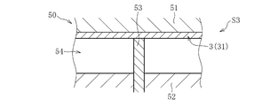
- the third step S3 first, as shown in FIG. 10A, the upper mold 51 and the lower mold 52 of the molding die 50 are moved relatively close to each other (the molding die 50 is clamped), and the upper mold 51 and the lower mold 52 are moved.
- the antenna pattern 3 is arranged as an insert part in a cavity 54 defined between the molds 52.
- a part of the molding die 50 for molding the top wall 21 of the base 2 is provided with a plurality of pins 53 that can be moved up and down relative to the lower mold 52, and the antenna pattern 3 is inserted into the cavity 54 as an insert part.
- the pin 53 moves upward and the upper surface of the antenna portion 31 of the antenna pattern 3 is pressed against the lower surface of the upper die 51 (the antenna portion 31 is clamped and fixed between the upper die 51 and the pin 53). It has become.
- a molten resin P PPS, LCP, PA or the like as a base resin and a filler such as ceramics blended therein
- PPS molten resin
- LCP low-density polystylene
- PA molten resin
- the molding die 50 is opened after the resin P is solidified, the chip antenna 1 connected to the frame 41 of the hoop material 40 through the bridge 42 is obtained.
- the pin 53 can also be provided integrally with the lower mold 52. In this case, as the molding die 50 is clamped, the antenna portion 31 of the antenna pattern 3 is sandwiched and fixed by the upper die 51 and the pin 53.
- the base body 2 is injection-molded with resin integrally with the antenna pattern 3 connected to the frame 41 of the hoop material 40, and the chip antenna 1 composed of the base body 2 and the antenna pattern 3 is obtained, it is connected to the frame 41 of the hoop material 40.
- the chip antenna 1 is supplied to the fourth step S4. Thereby, the molded product (chip antenna 1) is separated from the frame 41 of the hoop material 40.
- the fourth step S4 for separating the chip antenna 1 from the hoop material 40 is not necessarily provided downstream from the third step S3. That is, on the downstream side of the third step S3, instead of the fourth step S4 for separating the chip antenna 1 from the hoop material 40, the chip antenna 1 (the antenna pattern 3) is connected to the frame 41 via the bridge 42. You may provide the winding-up process which winds up the hoop material 40 with which it was connected in roll shape. Thus, if the hoop material 40 is wound up without separating the chip antenna 1 from the frame 41, the chip antenna 1 can be easily stored and transported and the aligned state of the chip antenna 1 can be maintained. Contact (interference) between one another can be prevented.
- the base 2 is erected along the rectangular plate-like top wall 21 and the long side direction of the top wall 21, and has one end (upper end) in the short side direction.
- a rectangular plate-like vertical wall 22 connected to the top wall 21 each part of the base 2 can be thinned (thinned) to reduce the amount of sink marks caused by molding shrinkage.
- the rigidity (bending rigidity) of the top wall 21 can be increased to prevent the base body 2 from being warped or bent in the direction along the long side of the top wall 21 as much as possible. Therefore, the antenna part 3 of the antenna pattern 1 can be stably held on the surface of the base 2 (top wall 21), and desired antenna characteristics can be exhibited.
- the usage-amount of resin can be restrained and cost reduction can be aimed at.
- the base body 2 of the present embodiment has a concave shape (reverse concave shape) in which the vertical wall 22 is erected along the two long sides of the top wall 21, so that the rigidity of the chip antenna 1 is effectively increased. Can be increased.
- the antenna pattern 3 is provided with the protrusion 34 embedded in the inside of the base 2, the holding power of the antenna pattern 3 with respect to the base 2 can be increased.
- the projecting portion 34 is provided on the antenna portion 31 of the antenna pattern 3, the antenna portion 31 is effectively peeled off from the base 2 (a part of the antenna portion 31 is lifted from the base 2). Can be prevented.
- the base body 2 constituting the chip antenna 1 is opened on both the front and back surfaces of the top wall 21 at a position directly below the antenna portion 31 of the antenna pattern 3, and the inner wall surface is a through hole formed by the molding die 50 of the base body 2. 25.
- the base body 2 is injection-molded in a state where the antenna portion 31 of the antenna pattern 3 is appropriately positioned and arranged on the surface side of the top wall 21. Therefore, the shape accuracy of the top wall 21 (base 2) and the positional accuracy of the antenna portion 31 with respect to the top wall 21 can be improved, and thus desired antenna characteristics can be exhibited.
- the present invention is not limited to the above embodiment. That is, the chip antenna 1 according to the present invention can take an arbitrary shape as long as the base 2 can be injection-molded with resin using the three-dimensional antenna pattern 3 as an insert part.
- the base plate 2 has a rectangular plate-like top with the antenna portion 31 held on the surface (upper surface) so that the cross section perpendicular to the long side direction is L-shaped (reverse L-shaped).
- the wall 21 and a rectangular plate-like vertical wall 22 erected along one long side of the top wall 21 can be used. Even in this case, the end walls 23 can be provided at both ends of the top wall 21 in the long side direction.
- the shape of the antenna pattern 3 described above is merely an example, and can be appropriately changed according to required antenna characteristics.
Abstract
L'invention porte sur une antenne à puce (1) comprenant : un motif d'antenne (3) qui est réalisé par pliage/cintrage d'une plaque électroconductrice dans une forme en trois dimensions, et qui comprend une partie d'antenne (31) et une partie de borne (32) qui est connectée électriquement à un substrat de circuit (10) ; et un corps de base (2) qui est moulé par injection par une résine, et qui comprend le motif d'antenne (3) en tant que composant d'insert. Le corps de base (2) comprend : une paroi supérieure en forme de plaque rectangulaire (21) qui maintient la partie d'antenne (31) sur la surface de cette dernière ; et une paroi verticale en forme de plaque rectangulaire (22) qui est disposée verticalement le long de la direction de côté long de la paroi supérieure (21), une extrémité (l'extrémité supérieure) de la paroi verticale dans la direction de côté court étant reliée à la paroi supérieure (21), et l'autre extrémité (l'extrémité inférieure) de cette dernière dans la direction de côté court maintenant la partie de borne (32).
Priority Applications (3)
| Application Number | Priority Date | Filing Date | Title |
|---|---|---|---|
| CN201580008509.3A CN105993097A (zh) | 2014-03-20 | 2015-03-06 | 芯片天线 |
| US15/127,241 US20170110783A1 (en) | 2014-03-20 | 2015-03-06 | Chip antenna |
| EP15765059.9A EP3121896A4 (fr) | 2014-03-20 | 2015-03-06 | Antenne à puce |
Applications Claiming Priority (2)
| Application Number | Priority Date | Filing Date | Title |
|---|---|---|---|
| JP2014-058022 | 2014-03-20 | ||
| JP2014058022A JP2015185881A (ja) | 2014-03-20 | 2014-03-20 | チップアンテナ |
Publications (1)
| Publication Number | Publication Date |
|---|---|
| WO2015141492A1 true WO2015141492A1 (fr) | 2015-09-24 |
Family
ID=54144465
Family Applications (1)
| Application Number | Title | Priority Date | Filing Date |
|---|---|---|---|
| PCT/JP2015/056602 WO2015141492A1 (fr) | 2014-03-20 | 2015-03-06 | Antenne à puce |
Country Status (5)
| Country | Link |
|---|---|
| US (1) | US20170110783A1 (fr) |
| EP (1) | EP3121896A4 (fr) |
| JP (1) | JP2015185881A (fr) |
| CN (1) | CN105993097A (fr) |
| WO (1) | WO2015141492A1 (fr) |
Families Citing this family (2)
| Publication number | Priority date | Publication date | Assignee | Title |
|---|---|---|---|---|
| JP6509296B2 (ja) * | 2017-10-03 | 2019-05-08 | 三菱電機株式会社 | 無線受信装置 |
| JP7088409B2 (ja) * | 2019-04-03 | 2022-06-21 | 株式会社村田製作所 | モジュール、端子集合体、及びモジュールの製造方法 |
Citations (7)
| Publication number | Priority date | Publication date | Assignee | Title |
|---|---|---|---|---|
| JP2002252514A (ja) * | 2001-02-22 | 2002-09-06 | Murata Mfg Co Ltd | 複共振アンテナ |
| JP2002330025A (ja) * | 2001-05-02 | 2002-11-15 | Murata Mfg Co Ltd | アンテナ装置及びこのアンテナ装置を備えた無線通信機 |
| JP2003324310A (ja) * | 2002-05-01 | 2003-11-14 | Furukawa Electric Co Ltd:The | 小型アンテナ |
| JP2004522347A (ja) * | 2001-03-20 | 2004-07-22 | コーニンクレッカ フィリップス エレクトロニクス エヌ ヴィ | 基体及び導体トラック構体を有するアンテナ |
| JP2005005883A (ja) * | 2003-06-10 | 2005-01-06 | Murata Mfg Co Ltd | 指向性アンテナ及びそのアンテナを用いた無線通信機並びにアンテナの指向性改善方法 |
| JP2010259043A (ja) * | 2009-04-23 | 2010-11-11 | Samsung Electro-Mechanics Co Ltd | アンテナパターンフレーム、その製造方法及び製造金型 |
| JP2013197678A (ja) * | 2012-03-16 | 2013-09-30 | Ntn Corp | マルチバンドアンテナ及びその製造方法 |
Family Cites Families (3)
| Publication number | Priority date | Publication date | Assignee | Title |
|---|---|---|---|---|
| US20020075186A1 (en) * | 2000-12-20 | 2002-06-20 | Hiroki Hamada | Chip antenna and method of manufacturing the same |
| KR101055786B1 (ko) * | 2010-07-26 | 2011-08-09 | (주)파트론 | 멀티밴드 칩 안테나 실장용 기판 및 이를 포함하는 멀티밴드 칩 안테나 장치 |
| JP5730523B2 (ja) * | 2010-09-28 | 2015-06-10 | Ntn株式会社 | チップアンテナ及びその製造方法 |
-
2014
- 2014-03-20 JP JP2014058022A patent/JP2015185881A/ja active Pending
-
2015
- 2015-03-06 US US15/127,241 patent/US20170110783A1/en not_active Abandoned
- 2015-03-06 EP EP15765059.9A patent/EP3121896A4/fr not_active Withdrawn
- 2015-03-06 CN CN201580008509.3A patent/CN105993097A/zh active Pending
- 2015-03-06 WO PCT/JP2015/056602 patent/WO2015141492A1/fr active Application Filing
Patent Citations (7)
| Publication number | Priority date | Publication date | Assignee | Title |
|---|---|---|---|---|
| JP2002252514A (ja) * | 2001-02-22 | 2002-09-06 | Murata Mfg Co Ltd | 複共振アンテナ |
| JP2004522347A (ja) * | 2001-03-20 | 2004-07-22 | コーニンクレッカ フィリップス エレクトロニクス エヌ ヴィ | 基体及び導体トラック構体を有するアンテナ |
| JP2002330025A (ja) * | 2001-05-02 | 2002-11-15 | Murata Mfg Co Ltd | アンテナ装置及びこのアンテナ装置を備えた無線通信機 |
| JP2003324310A (ja) * | 2002-05-01 | 2003-11-14 | Furukawa Electric Co Ltd:The | 小型アンテナ |
| JP2005005883A (ja) * | 2003-06-10 | 2005-01-06 | Murata Mfg Co Ltd | 指向性アンテナ及びそのアンテナを用いた無線通信機並びにアンテナの指向性改善方法 |
| JP2010259043A (ja) * | 2009-04-23 | 2010-11-11 | Samsung Electro-Mechanics Co Ltd | アンテナパターンフレーム、その製造方法及び製造金型 |
| JP2013197678A (ja) * | 2012-03-16 | 2013-09-30 | Ntn Corp | マルチバンドアンテナ及びその製造方法 |
Non-Patent Citations (1)
| Title |
|---|
| See also references of EP3121896A4 * |
Also Published As
| Publication number | Publication date |
|---|---|
| CN105993097A (zh) | 2016-10-05 |
| EP3121896A1 (fr) | 2017-01-25 |
| JP2015185881A (ja) | 2015-10-22 |
| EP3121896A4 (fr) | 2017-11-22 |
| US20170110783A1 (en) | 2017-04-20 |
Similar Documents
| Publication | Publication Date | Title |
|---|---|---|
| KR101585598B1 (ko) | 안테나 모듈의 제조 방법, 그리고 사출 성형물 속에 안테나 방사체가 내장된 전자기기용 내장형 안테나의 제조방법 | |
| US20100039347A1 (en) | Housing functioning as an antenna and method for fabricating the same | |
| JP2012044654A (ja) | 電子装置用ケース体及びその製作方法 | |
| JP2010220217A (ja) | 移動通信端末機ケースの製造方法、これを利用した移動通信端末機ケース及び移動通信端末機 | |
| WO2017047380A1 (fr) | Antenne de puce et son procédé de fabrication | |
| CN100358184C (zh) | 小型天线及其制造方法 | |
| JP4503604B2 (ja) | 電子パッケージ及びそれを構成する方法 | |
| JP2023036857A (ja) | 基板接続コネクタ向けの端子、コネクタ及びコネクタ製造方法 | |
| WO2015141492A1 (fr) | Antenne à puce | |
| JP5730523B2 (ja) | チップアンテナ及びその製造方法 | |
| US9912056B2 (en) | Multiband antenna and manufacturing method thereof | |
| US20160224061A1 (en) | Electrical device and method of producing the same | |
| JP6370617B2 (ja) | チップアンテナ | |
| JP2009044735A (ja) | 移動機器及びその製造方法 | |
| KR100861102B1 (ko) | 표면 실장형 인덕터의 단자 형성 방법 | |
| KR102293941B1 (ko) | 3d 프린팅 방법에 의해 하우징이 형성되는 전자 장치 | |
| TWI578615B (zh) | 天線結構、應用其的電子裝置及其製作方法 | |
| US10559478B2 (en) | Method for manufacturing electronic device and electronic device | |
| JP2003078342A (ja) | チップアンテナとその製造方法 | |
| KR20170033523A (ko) | 금형 및 이를 이용한 안테나 제조방법 | |
| KR101370499B1 (ko) | 전자기기용 내장형 안테나의 제조방법 | |
| KR20170029958A (ko) | 안테나 제조를 위한 연성인쇄회로기판 및 이의 제조방법 | |
| JP2002198719A (ja) | 小型アンテナ |
Legal Events
| Date | Code | Title | Description |
|---|---|---|---|
| 121 | Ep: the epo has been informed by wipo that ep was designated in this application |
Ref document number: 15765059 Country of ref document: EP Kind code of ref document: A1 |
|
| WWE | Wipo information: entry into national phase |
Ref document number: 15127241 Country of ref document: US |
|
| NENP | Non-entry into the national phase |
Ref country code: DE |
|
| REEP | Request for entry into the european phase |
Ref document number: 2015765059 Country of ref document: EP |
|
| WWE | Wipo information: entry into national phase |
Ref document number: 2015765059 Country of ref document: EP |