WO2015141492A1 - Chip antenna - Google Patents
Chip antenna Download PDFInfo
- Publication number
- WO2015141492A1 WO2015141492A1 PCT/JP2015/056602 JP2015056602W WO2015141492A1 WO 2015141492 A1 WO2015141492 A1 WO 2015141492A1 JP 2015056602 W JP2015056602 W JP 2015056602W WO 2015141492 A1 WO2015141492 A1 WO 2015141492A1
- Authority
- WO
- WIPO (PCT)
- Prior art keywords
- antenna
- top wall
- chip antenna
- chip
- pattern
- Prior art date
Links
Images


Classifications
-
- H—ELECTRICITY
- H01—ELECTRIC ELEMENTS
- H01Q—ANTENNAS, i.e. RADIO AERIALS
- H01Q1/00—Details of, or arrangements associated with, antennas
- H01Q1/12—Supports; Mounting means
- H01Q1/22—Supports; Mounting means by structural association with other equipment or articles
- H01Q1/2283—Supports; Mounting means by structural association with other equipment or articles mounted in or on the surface of a semiconductor substrate as a chip-type antenna or integrated with other components into an IC package
-
- H—ELECTRICITY
- H01—ELECTRIC ELEMENTS
- H01Q—ANTENNAS, i.e. RADIO AERIALS
- H01Q1/00—Details of, or arrangements associated with, antennas
- H01Q1/12—Supports; Mounting means
- H01Q1/22—Supports; Mounting means by structural association with other equipment or articles
- H01Q1/2291—Supports; Mounting means by structural association with other equipment or articles used in bluetooth or WI-FI devices of Wireless Local Area Networks [WLAN]
-
- H—ELECTRICITY
- H01—ELECTRIC ELEMENTS
- H01Q—ANTENNAS, i.e. RADIO AERIALS
- H01Q1/00—Details of, or arrangements associated with, antennas
- H01Q1/36—Structural form of radiating elements, e.g. cone, spiral, umbrella; Particular materials used therewith
- H01Q1/38—Structural form of radiating elements, e.g. cone, spiral, umbrella; Particular materials used therewith formed by a conductive layer on an insulating support
-
- H—ELECTRICITY
- H01—ELECTRIC ELEMENTS
- H01Q—ANTENNAS, i.e. RADIO AERIALS
- H01Q9/00—Electrically-short antennas having dimensions not more than twice the operating wavelength and consisting of conductive active radiating elements
- H01Q9/04—Resonant antennas
- H01Q9/30—Resonant antennas with feed to end of elongated active element, e.g. unipole
- H01Q9/42—Resonant antennas with feed to end of elongated active element, e.g. unipole with folded element, the folded parts being spaced apart a small fraction of the operating wavelength
Definitions
- the present invention relates to a chip antenna incorporated in a wireless communication device having a wireless communication function such as a mobile phone (including a smartphone), a tablet PC, a smart meter (digital watt hour meter), and the like.
- a wireless communication device having a wireless communication function such as a mobile phone (including a smartphone), a tablet PC, a smart meter (digital watt hour meter), and the like.
- a chip-like antenna that can be mounted on the surface of a circuit board is preferably used as an antenna incorporated in this type of wireless communication device.
- This chip antenna includes a chip-shaped base made of a resin having a high dielectric constant and an antenna pattern made of a conductor formed on the surface of the base. For example, a step of forming a conductor film on the surface of the base made of resin A step of forming a mask pattern corresponding to the antenna pattern shape on the conductor film, and a conductive film region exposed from the mask pattern is removed by etching, and then the desired antenna is formed on the substrate by removing the mask pattern. It can be manufactured through a process of forming a pattern.
- Patent Document 1 a chip antenna comprising an antenna pattern formed by bending a conductive plate into a three-dimensional shape, and a base that is injection-molded with resin using the three-dimensional antenna pattern as an insert part.
- a rectangular parallelepiped base may be thinned.
- the substrate since the rigidity of the substrate is greatly reduced only by thinning the substrate, the substrate may be greatly deformed with a temperature change or the like, for example. In this case, it becomes more difficult to hold the antenna pattern on the surface.
- an object of the present invention is to reduce the cost of a chip antenna that can prevent deformation of a base body due to molding shrinkage and temperature change as much as possible, and thereby stably exhibit desired antenna characteristics. There is to provide to.
- the present invention has an antenna pattern in which a conductive plate is bent into a three-dimensional shape and has an antenna part and a terminal part electrically connected to a circuit board, and the antenna pattern is inserted.
- a chip antenna including a base body that is injection-molded with resin as a component, the base body is provided with a rectangular plate-like top wall that holds the antenna portion on the surface, and a short side that is erected along the long side direction of the top wall. One end in the direction is connected to the top wall, and the other end in the short side direction is provided with a rectangular plate-like vertical wall holding the terminal portion.
- the antenna unit is a part that performs at least one of transmission and reception of radio waves.
- the base body is provided with a rectangular plate-like top wall and a rectangular plate-like vertical wall that is erected along the long side direction of the top wall and one end in the short side direction is connected to the top wall.
- each part of the base can be thinned (thinned) to reduce the amount of sink marks caused by molding shrinkage, and the top wall rigidity (bending rigidity) can be increased to increase the length of the top wall. It is possible to prevent as much as possible the warping / bending of the substrate in the direction along. Therefore, the antenna portion of the antenna pattern can be stably held on the surface of the base body (top wall), and desired antenna characteristics can be exhibited.
- the usage-amount of resin can be restrained and cost reduction can be aimed at.
- the base body can take any shape as long as a three-dimensional antenna pattern can be injection molded as an insert part.
- a vertical wall can be provided along the two long sides of the top wall.
- the base body (chip antenna) exhibits a concave shape (reverse concave shape) in an arbitrary cross section in a direction orthogonal to the long side direction, so that the rigidity of the chip antenna can be effectively increased.
- the antenna pattern is provided with a protrusion embedded in the substrate, the holding power of the antenna pattern with respect to the substrate can be increased.
- the above-mentioned protrusion is provided on the antenna portion of the antenna pattern, it is possible to effectively prevent the antenna portion from being peeled off from the base, so that desired antenna characteristics can be stably exhibited. Is preferable.
- the chip antenna having the above-described configuration can be provided with a through-hole that is opened on the top and bottom surfaces of the top wall at a position directly below the antenna portion of the antenna pattern and whose inner wall surface is formed by a base molding die.
- the substrate is injection-molded in a state where the antenna portion of the antenna pattern is appropriately arranged on the surface side of the top wall. Accordingly, the shape accuracy of the top wall (base body) and the position accuracy of the antenna portion with respect to the top wall can be improved, so that desired antenna characteristics can be exhibited.
- At least the surface roughness of the bonding surface of the conductive plate constituting the antenna pattern is Ra 1.6 or more.
- the base molding resin preferably has a high dielectric constant from the viewpoint of securing desired antenna characteristics, and specifically, a resin having a dielectric constant of 4 or more is preferable.
- the resin having a dielectric constant of 4 or higher is not necessarily limited to a base resin having a dielectric constant of 4 or higher, but includes a resin having a dielectric constant of 4 or higher as a whole by blending of fillers.
- FIG. 3 is a cross-sectional view of the chip antenna, taken along the line EE shown in FIG.
- FIG. 3 is a cross-sectional view of the chip antenna, taken along the line FF shown in FIG. FIG.
- FIG. 3 is a cross-sectional view of the chip antenna, taken along the line GG shown in FIG.
- FIG. 7 is a process explanatory diagram for manufacturing the chip antenna shown in FIGS. 1 to 6; It is a figure which shows typically the clamping state of the molding die for injection-molding the base
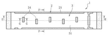
- FIG. 1 is a schematic perspective view of a circuit board 10 on which a chip antenna 1 according to an embodiment of the present invention is mounted.
- a chip antenna 1 shown in FIG. 1 includes an antenna pattern 3 made of a conductive plate, and a base body 2 injection-molded with a resin using the antenna pattern 3 as an insert part.
- the total length of the chip antenna 1 (the dimension in the left-right direction in FIG. 2) varies depending on the frequency (wavelength) of radio waves transmitted and received by the chip antenna 1, but is about 10 to 50 mm, for example.
- the upper direction, the lower direction, the left direction, and the right direction in FIG. 1 are respectively “up”, “down”, “left”, and “right”.
- the usage mode of the chip antenna 1 is not limited.
- the antenna pattern 3 is formed by bending a conductive plate into a three-dimensional shape, and as shown in FIGS. 2 to 7, an antenna unit 31 for transmitting and receiving radio waves and a plurality of terminal units 32 (the book) 7 in the embodiment) and a plurality of connection portions 33 for connecting the antenna portion 31 and each terminal portion 32 are integrally provided.
- radio waves are also transmitted and received by the connection unit 33, but the amount of radio waves transmitted and received by the connection unit 33 is negligibly small compared to the amount of radio waves transmitted and received by the antenna unit 31.
- a conductive plate for example, a metal plate such as a copper plate, a steel plate, or a SUS plate, or a plate obtained by plating these metal plates, and the plate thickness can be maintained within a range where a desired three-dimensional shape can be maintained as much as possible.
- the one set thinly for example, 1 mm or less, more preferably 0.5 mm or less
- the surface roughness of the joint surface of the antenna pattern 3 (conductive plate) with the substrate 2 is set to Ra 1.6 or more, preferably 3.2 or more.
- At least one of the plurality (seven) terminal portions 32 of the antenna pattern 3 functions as a power supply terminal electrically connected to the power supply line of the circuit board 10, and at least one of the remaining terminal portions 32.
- One functions as a ground terminal for grounding the antenna pattern 3 to the ground via the circuit board 10.
- the terminal portion 32 other than the power supply terminal and the ground terminal functions as a fixing portion for fixing the chip antenna 1 to the circuit board 10.
- the base 2 is injection-molded with resin using the antenna pattern 3 as an insert part.
- the molding resin for the substrate 2 one having a dielectric constant of 4 or more is selectively used.
- PPS polyphenylene sulfide
- LCP liquid crystal polymer
- PA polyamide
- thermoplastic resins can be used as a base resin, which is mixed with a filler such as ceramics.
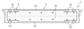
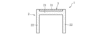
- the base body 2 is erected along a rectangular plate-like top wall 21 holding the antenna portion 31 of the antenna pattern 3 on the surface (upper surface) and two long sides of the top wall 21, and has one end (upper end) in the short side direction. ) Are connected to the top wall 21 and are provided with rectangular plate-like vertical walls 22 and 22 holding the terminal portions 32 of the antenna pattern 3 at the other end (lower end surface) in the short side direction.
- the end walls 23 and 23 are further provided at both ends of the top wall 21 in the long side direction. That is, the base body 2 of the present embodiment has a concave shape (reverse concave shape) in the cross-sectional shape of each part in the long side direction except for both ends in the long side direction.
- the thicknesses of the top wall 21, the pair of vertical walls 22 and the pair of end walls 23, 23 are set to be approximately equal within a range of 0.5 mm to 2.0 mm, for example.
- the three connection parts 33 included in the antenna pattern 3 are held on the surface (left side surface) of the left vertical wall 22, and the four connection parts 33 is held on the surface (right side surface) of the right vertical wall 22.
- the seven terminal portions 32 of the antenna pattern 3 are held on the lower end surface of the left vertical wall 22, and the four terminal portions 32 are on the lower end surface of the right vertical wall 22. It is held (see FIG. 5).
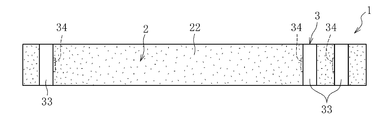
- the antenna pattern 3 has a protrusion 34 embedded in the base 2.
- the antenna portion 31 is provided with five protrusions 34, and each connection portion 33 is provided with one protrusion 34. In this way, the holding force of the antenna pattern 3 with respect to the base 2 can be increased.
- the projecting portion 34 is provided on the antenna portion 31, it is possible to effectively prevent the antenna portion 31 from peeling (raising) from the base body 2 (top wall 21), so that the desired antenna characteristics can be stabilized. This is advantageous in that it can be exhibited.
- the protrusion part 34 provided in the antenna part 31 is the antenna part 31 (more specifically, the part used as the antenna part 31 among the expansion
- This is formed by bending a tongue-like portion formed by forming a slit penetrating the front and back surfaces of the front and back surfaces to the back surface side with the base end as a fulcrum (see FIG. 8).
- the slit is formed in a U-shape, but may be formed in other shapes such as a semicircle. Further, in the present embodiment, as shown in FIG.
- the protruding portion 34 is formed by bending the tongue piece-like portion 90 ° to the back side, but the bending angle of the tongue piece-like portion is arbitrarily set. Is possible.
- one protrusion 34 provided on each connection portion 33 is formed by bending a tongue-like portion formed on a hoop material 40 (deployment pattern 3 ′) as a conductive plate by punching press processing. (See FIG. 9).
- substrate 2 has the several through-hole 25 opened on the front and back both surfaces, as shown in FIG.
- Each through hole 25 is open on both the front and back surfaces of the top wall 21 at a position directly below the antenna portion 31, and the inner wall surface thereof is formed with a molding surface formed by a molding die 50 (see FIG. 10) of the base 2. Is done.
- the chip antenna 1 of this embodiment includes a long conductive plate (hoop material 40), a first step S1 for forming the development pattern 3 ′, a second step S2 for forming the antenna pattern 3, and a base body. 2 is manufactured by sequentially supplying to a third step S3 for injection molding 2 and a fourth step S4 for taking out the chip antenna 1.
- the second step S2 is performed in multiple times (four times).
- a development pattern 3 'in which the three-dimensional antenna pattern 3 is developed on a plane is formed by punching a part of the hoop material 40 with a press mold (not shown).
- the development pattern 3 ′ is connected to the frame 41 of the hoop material 40 via the bridge 42.
- Reference numeral 43 shown in FIG. 9 is a positioning hole of the hoop material 40 with respect to a conveying device (not shown).
- the hoop material 40 is conveyed downward in FIG. 9, and the portion of the hoop material 40 where the development pattern 3 ′ is formed is sequentially applied to the first to fourth stages of the second step S2. Supplied.
- the second step S2 in the first stage, a slit is formed in a portion of the development pattern 3 ′ that becomes the antenna portion 31 of the antenna pattern 3, and thereafter, in the second to fourth stages, the development pattern 3 ′ is sequentially formed. Bending is applied.
- the three-dimensional antenna pattern 3 having the antenna portion 31, the terminal portion 32, and the connection portion 33 integrally formed on the hoop material 40, and the projection portion 34 formed on the antenna portion 31 and the connection portion 33 is formed.
- the antenna pattern 3 formed on the hoop material 40 is connected to a frame 41 via a bridge 42.
- the slit forming process performed in the first stage of the second step S2 is performed using, for example, a punching press mold, and the bending processes performed in the second to fourth stages are performed in the bending press mold. Alternatively, it is executed using an actuator such as an air cylinder or a hydraulic cylinder.
- the hoop material 40 is further conveyed to the downstream side, and the portion where the antenna pattern 3 is formed is supplied to the third step S3.
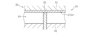
- the third step S3 first, as shown in FIG. 10A, the upper mold 51 and the lower mold 52 of the molding die 50 are moved relatively close to each other (the molding die 50 is clamped), and the upper mold 51 and the lower mold 52 are moved.
- the antenna pattern 3 is arranged as an insert part in a cavity 54 defined between the molds 52.
- a part of the molding die 50 for molding the top wall 21 of the base 2 is provided with a plurality of pins 53 that can be moved up and down relative to the lower mold 52, and the antenna pattern 3 is inserted into the cavity 54 as an insert part.
- the pin 53 moves upward and the upper surface of the antenna portion 31 of the antenna pattern 3 is pressed against the lower surface of the upper die 51 (the antenna portion 31 is clamped and fixed between the upper die 51 and the pin 53). It has become.
- a molten resin P PPS, LCP, PA or the like as a base resin and a filler such as ceramics blended therein
- PPS molten resin
- LCP low-density polystylene
- PA molten resin
- the molding die 50 is opened after the resin P is solidified, the chip antenna 1 connected to the frame 41 of the hoop material 40 through the bridge 42 is obtained.
- the pin 53 can also be provided integrally with the lower mold 52. In this case, as the molding die 50 is clamped, the antenna portion 31 of the antenna pattern 3 is sandwiched and fixed by the upper die 51 and the pin 53.
- the base body 2 is injection-molded with resin integrally with the antenna pattern 3 connected to the frame 41 of the hoop material 40, and the chip antenna 1 composed of the base body 2 and the antenna pattern 3 is obtained, it is connected to the frame 41 of the hoop material 40.
- the chip antenna 1 is supplied to the fourth step S4. Thereby, the molded product (chip antenna 1) is separated from the frame 41 of the hoop material 40.
- the fourth step S4 for separating the chip antenna 1 from the hoop material 40 is not necessarily provided downstream from the third step S3. That is, on the downstream side of the third step S3, instead of the fourth step S4 for separating the chip antenna 1 from the hoop material 40, the chip antenna 1 (the antenna pattern 3) is connected to the frame 41 via the bridge 42. You may provide the winding-up process which winds up the hoop material 40 with which it was connected in roll shape. Thus, if the hoop material 40 is wound up without separating the chip antenna 1 from the frame 41, the chip antenna 1 can be easily stored and transported and the aligned state of the chip antenna 1 can be maintained. Contact (interference) between one another can be prevented.
- the base 2 is erected along the rectangular plate-like top wall 21 and the long side direction of the top wall 21, and has one end (upper end) in the short side direction.
- a rectangular plate-like vertical wall 22 connected to the top wall 21 each part of the base 2 can be thinned (thinned) to reduce the amount of sink marks caused by molding shrinkage.
- the rigidity (bending rigidity) of the top wall 21 can be increased to prevent the base body 2 from being warped or bent in the direction along the long side of the top wall 21 as much as possible. Therefore, the antenna part 3 of the antenna pattern 1 can be stably held on the surface of the base 2 (top wall 21), and desired antenna characteristics can be exhibited.
- the usage-amount of resin can be restrained and cost reduction can be aimed at.
- the base body 2 of the present embodiment has a concave shape (reverse concave shape) in which the vertical wall 22 is erected along the two long sides of the top wall 21, so that the rigidity of the chip antenna 1 is effectively increased. Can be increased.
- the antenna pattern 3 is provided with the protrusion 34 embedded in the inside of the base 2, the holding power of the antenna pattern 3 with respect to the base 2 can be increased.
- the projecting portion 34 is provided on the antenna portion 31 of the antenna pattern 3, the antenna portion 31 is effectively peeled off from the base 2 (a part of the antenna portion 31 is lifted from the base 2). Can be prevented.
- the base body 2 constituting the chip antenna 1 is opened on both the front and back surfaces of the top wall 21 at a position directly below the antenna portion 31 of the antenna pattern 3, and the inner wall surface is a through hole formed by the molding die 50 of the base body 2. 25.
- the base body 2 is injection-molded in a state where the antenna portion 31 of the antenna pattern 3 is appropriately positioned and arranged on the surface side of the top wall 21. Therefore, the shape accuracy of the top wall 21 (base 2) and the positional accuracy of the antenna portion 31 with respect to the top wall 21 can be improved, and thus desired antenna characteristics can be exhibited.
- the present invention is not limited to the above embodiment. That is, the chip antenna 1 according to the present invention can take an arbitrary shape as long as the base 2 can be injection-molded with resin using the three-dimensional antenna pattern 3 as an insert part.
- the base plate 2 has a rectangular plate-like top with the antenna portion 31 held on the surface (upper surface) so that the cross section perpendicular to the long side direction is L-shaped (reverse L-shaped).
- the wall 21 and a rectangular plate-like vertical wall 22 erected along one long side of the top wall 21 can be used. Even in this case, the end walls 23 can be provided at both ends of the top wall 21 in the long side direction.
- the shape of the antenna pattern 3 described above is merely an example, and can be appropriately changed according to required antenna characteristics.
Abstract
Disclosed is a chip antenna (1) comprising: an antenna pattern (3) that is made by folding/bending an electroconductive plate into a three-dimensional shape, and that includes an antenna part (31) and a terminal part (32) that is electrically connected to a circuit substrate (10); and a base body (2) that is injection-molded by a resin, and that includes the antenna pattern (3) as an insert component. The base body (2) includes: a rectangular plate-form top wall (21) that holds the antenna part (31) on the surface thereof; and a rectangular plate-form vertical wall (22) that is provided upright along the long-side direction of the top wall (21), wherein one end (the upper end) of the vertical wall in the short-side direction is connected to the top wall (21), and the other end (the lower end) thereof in the short-side direction holds the terminal part (32).
Description
本発明は、例えば携帯電話(スマートフォンを含む)、タブレット型のPC、スマートメータ(デジタル式の電力量計)等、無線通信機能を備えた無線通信機器に組み込まれるチップアンテナに関する。
The present invention relates to a chip antenna incorporated in a wireless communication device having a wireless communication function such as a mobile phone (including a smartphone), a tablet PC, a smart meter (digital watt hour meter), and the like.
スマートフォンやタブレット型のPC等、近年急速に普及している携帯型の無線通信機器は、一層の小型化や薄型化が進展している。そこで、この種の無線通信機器に組み込まれるアンテナとしては、回路基板の表面に実装可能なチップ状のアンテナ(チップアンテナ)が好適に使用される。
Portable wireless communication devices such as smartphones and tablet PCs, which have been rapidly spreading in recent years, have been further reduced in size and thickness. Therefore, a chip-like antenna (chip antenna) that can be mounted on the surface of a circuit board is preferably used as an antenna incorporated in this type of wireless communication device.
チップアンテナの一例が下記の特許文献1に開示されている。このチップアンテナは、高誘電率の樹脂からなるチップ状の基体と、基体表面に形成された導電体からなるアンテナパターンとを備えており、例えば、樹脂製の基体表面に導体膜を形成する工程、導体膜上にアンテナパターン形状に対応したマスクパターンを形成する工程、および、マスクパターンから露出されている導体膜領域をエッチングにより除去した後、マスクパターンを除去することで基体上に所望のアンテナパターンを形成する工程などを経て製造することができる。
An example of a chip antenna is disclosed in Patent Document 1 below. This chip antenna includes a chip-shaped base made of a resin having a high dielectric constant and an antenna pattern made of a conductor formed on the surface of the base. For example, a step of forming a conductor film on the surface of the base made of resin A step of forming a mask pattern corresponding to the antenna pattern shape on the conductor film, and a conductive film region exposed from the mask pattern is removed by etching, and then the desired antenna is formed on the substrate by removing the mask pattern. It can be manufactured through a process of forming a pattern.
近年、チップアンテナの一層の小型化を図るべく、アンテナパターンを基体の複数表面に沿って形成する(アンテナパターンを立体形状化する)ことが検討されている。しかし、特許文献1に開示された技術手段は、手間のかかる複数工程が必要である関係上、コスト的に難があるばかりでなく、立体形状のアンテナパターンを精度良く形成するのが難しいという問題がある。そこで、本出願人は、導電板を立体形状に折り曲げてなるアンテナパターンと、この立体形状のアンテナパターンをインサート部品として樹脂で射出成形された基体とからなるチップアンテナを提案している(特許文献2参照)。
Recently, in order to further reduce the size of a chip antenna, it has been studied to form an antenna pattern along a plurality of surfaces of a substrate (to make the antenna pattern three-dimensional). However, the technical means disclosed in Patent Document 1 is not only difficult in terms of cost due to the need for laborious multiple processes, but also has a problem that it is difficult to accurately form a three-dimensional antenna pattern. There is. Therefore, the present applicant has proposed a chip antenna comprising an antenna pattern formed by bending a conductive plate into a three-dimensional shape, and a base that is injection-molded with resin using the three-dimensional antenna pattern as an insert part (Patent Literature). 2).
ところで、立体形状のアンテナパターンを備えたチップアンテナのアンテナ特性を安定的に発揮させるには、アンテナパターンのうち、特に電波の送受信を行うアンテナ部として機能する部分を基体表面に保持する必要がある。しかし、導電板を立体形状に折り曲げてなるアンテナパターンでは、例えば折り曲げ部の角度が弾性力により広がり、その結果、アンテナパターンが部分的に基体から剥離する可能性がある。そこで、特許文献2のチップアンテナでは、アンテナパターンの縁部に基体内部に埋め込まれる突起部を設ける、アンテナパターンのうち、少なくとも基体との接合面の表面粗さを粗くする、などの対策を講じることでアンテナパターンを基体表面に保持するようにしている。
By the way, in order to stably exhibit the antenna characteristics of a chip antenna having a three-dimensional antenna pattern, it is necessary to hold a portion of the antenna pattern that functions as an antenna unit for transmitting and receiving radio waves on the surface of the substrate. . However, in an antenna pattern formed by bending a conductive plate into a three-dimensional shape, for example, the angle of the bent portion is expanded by an elastic force, and as a result, the antenna pattern may partially peel from the base. Therefore, in the chip antenna of Patent Document 2, measures are taken such as providing a protrusion embedded in the base at the edge of the antenna pattern, or roughening at least the surface roughness of the joint surface with the base in the antenna pattern. Thus, the antenna pattern is held on the substrate surface.
しかしながら、特許文献2のチップアンテナのように、樹脂製の基体を厚肉の直方体状に形成すると、成形収縮に伴って基体に比較的大きな反りやヒケが生じる。特に、低周波数帯の電波を送受信する用途では、波長との関係でアンテナサイズを大きくする(チップアンテナを長寸化する)必要が生じるため、成形収縮に伴う基体の反り量(基体の長辺方向に沿う方向における反り量)が増大し易くなる。そのため、上述のような対策を講じたとしても、アンテナパターンの一部が基体表面から浮いた状態等になり易く、所望のアンテナ特性を発揮させるのが難しい。
However, when the resin base is formed in a thick rectangular parallelepiped shape as in the chip antenna of Patent Document 2, relatively large warpage and sink marks are generated in the base as the mold shrinks. In particular, in applications where radio waves in a low frequency band are transmitted and received, it is necessary to increase the antenna size (lengthening the chip antenna) in relation to the wavelength, so the amount of warpage of the substrate accompanying molding shrinkage (long side of the substrate) The amount of warping in the direction along the direction is likely to increase. For this reason, even if the above-described measures are taken, it is difficult for a part of the antenna pattern to be lifted from the surface of the substrate, and it is difficult to exert desired antenna characteristics.
成形収縮に伴うヒケ量を抑える観点から言えば、直方体状の基体を薄板化すれば良いとも考えられる。しかしながら、基体を薄板化するだけでは、基体の剛性が大きく低下してしまうため、例えば温度変化等に伴って基体が大きく変形するおそれがある。この場合、アンテナパターンを表面に保持することが一層難しくなる。
From the viewpoint of suppressing the amount of sink due to molding shrinkage, it is considered that a rectangular parallelepiped base may be thinned. However, since the rigidity of the substrate is greatly reduced only by thinning the substrate, the substrate may be greatly deformed with a temperature change or the like, for example. In this case, it becomes more difficult to hold the antenna pattern on the surface.
以上の実情に鑑み、本発明の目的は、成形収縮や温度変化に伴う基体の変形を可及的に防止し、これにより所望のアンテナ特性を安定的に発揮することのできるチップアンテナを低コストに提供することにある。
In view of the above circumstances, an object of the present invention is to reduce the cost of a chip antenna that can prevent deformation of a base body due to molding shrinkage and temperature change as much as possible, and thereby stably exhibit desired antenna characteristics. There is to provide to.
上記の目的を達成するために創案された本発明は、導電板を立体形状に折り曲げてなり、アンテナ部、および回路基板と電気的に接続される端子部を有するアンテナパターンと、アンテナパターンをインサート部品として樹脂で射出成形された基体とを備えるチップアンテナにおいて、基体は、上記アンテナ部を表面に保持した長方形板状の頂壁と、頂壁の長辺方向に沿って立設され、短辺方向の一端が頂壁に繋がると共に、短辺方向の他端に上記端子部を保持した長方形板状の縦壁とを備えることを特徴とする。なお、アンテナ部とは、電波の送信および受信の少なくとも一方を行う部位である。
In order to achieve the above object, the present invention has an antenna pattern in which a conductive plate is bent into a three-dimensional shape and has an antenna part and a terminal part electrically connected to a circuit board, and the antenna pattern is inserted. In a chip antenna including a base body that is injection-molded with resin as a component, the base body is provided with a rectangular plate-like top wall that holds the antenna portion on the surface, and a short side that is erected along the long side direction of the top wall. One end in the direction is connected to the top wall, and the other end in the short side direction is provided with a rectangular plate-like vertical wall holding the terminal portion. The antenna unit is a part that performs at least one of transmission and reception of radio waves.
このように、基体が、長方形板状の頂壁と、頂壁の長辺方向に沿って立設され、短辺方向の一端が頂壁に繋がった長方形板状の縦壁とを備えていれば、基体の各部を薄肉化(薄板化)して、成形収縮に伴って生じるヒケの量を抑えることができることに加え、頂壁の剛性(曲げ剛性)を高めて、頂壁の長辺に沿う方向で基体に反り・曲り等が生じるのを可及的に防止することができる。そのため、アンテナパターンのアンテナ部を基体(頂壁)表面に安定的に保持することが可能となり、所望のアンテナ特性を発揮することができる。また、上記構成によれば、樹脂の使用量を抑えてコスト低減を図ることができる。
Thus, the base body is provided with a rectangular plate-like top wall and a rectangular plate-like vertical wall that is erected along the long side direction of the top wall and one end in the short side direction is connected to the top wall. For example, each part of the base can be thinned (thinned) to reduce the amount of sink marks caused by molding shrinkage, and the top wall rigidity (bending rigidity) can be increased to increase the length of the top wall. It is possible to prevent as much as possible the warping / bending of the substrate in the direction along. Therefore, the antenna portion of the antenna pattern can be stably held on the surface of the base body (top wall), and desired antenna characteristics can be exhibited. Moreover, according to the said structure, the usage-amount of resin can be restrained and cost reduction can be aimed at.
基体は、立体形状のアンテナパターンをインサート部品として射出成形可能である限りにおいて任意形状をとることができ、例えば、頂壁の2つの長辺に沿って縦壁を設けることができる。この場合、基体(チップアンテナ)は、その長辺方向と直交する方向の任意断面において凹字状(逆凹字状)を呈するので、チップアンテナの剛性を効果的に高めることができる。
The base body can take any shape as long as a three-dimensional antenna pattern can be injection molded as an insert part. For example, a vertical wall can be provided along the two long sides of the top wall. In this case, the base body (chip antenna) exhibits a concave shape (reverse concave shape) in an arbitrary cross section in a direction orthogonal to the long side direction, so that the rigidity of the chip antenna can be effectively increased.
アンテナパターンに基体の内部に埋め込まれる突起部を設けておけば、基体に対するアンテナパターンの保持力を高めることができる。特に、アンテナパターンのアンテナ部に上記突起部を設けておけば、基体からアンテナ部が剥離等するのを効果的に防止することができるので、所望のアンテナ特性を安定的に発揮可能とする上で好ましい。
If the antenna pattern is provided with a protrusion embedded in the substrate, the holding power of the antenna pattern with respect to the substrate can be increased. In particular, if the above-mentioned protrusion is provided on the antenna portion of the antenna pattern, it is possible to effectively prevent the antenna portion from being peeled off from the base, so that desired antenna characteristics can be stably exhibited. Is preferable.
以上の構成を有するチップアンテナには、アンテナパターンのアンテナ部の直下位置で頂壁の表面および裏面に開口し、かつ内壁面が基体の成形金型で成形された貫通孔を設けることができる。これはすなわち、アンテナパターンのアンテナ部が、頂壁の表面側に適切に配置された状態で基体が射出成形されることを意味する。従って、頂壁(基体)の形状精度、さらには頂壁に対するアンテナ部の位置精度を高めることができるので、所望のアンテナ特性を発揮することができる。
The chip antenna having the above-described configuration can be provided with a through-hole that is opened on the top and bottom surfaces of the top wall at a position directly below the antenna portion of the antenna pattern and whose inner wall surface is formed by a base molding die. This means that the substrate is injection-molded in a state where the antenna portion of the antenna pattern is appropriately arranged on the surface side of the top wall. Accordingly, the shape accuracy of the top wall (base body) and the position accuracy of the antenna portion with respect to the top wall can be improved, so that desired antenna characteristics can be exhibited.
アンテナパターンと基体との密着力を一層高めるため、アンテナパターンを構成する導電板のうち、少なくとも基体との接合面の面粗度はRa1.6以上であることが好ましい。
In order to further enhance the adhesion between the antenna pattern and the substrate, it is preferable that at least the surface roughness of the bonding surface of the conductive plate constituting the antenna pattern is Ra 1.6 or more.
基体の成形用樹脂としては、所望のアンテナ特性を確保する観点から高い誘電率を具備するものが好ましく、具体的には、誘電率4以上の樹脂が好ましい。なお、誘電率4以上の樹脂とは、必ずしもベース樹脂の誘電率が4以上のものに限定されるわけではなく、充填材の配合により樹脂全体として誘電率が4以上になるものを含む。
The base molding resin preferably has a high dielectric constant from the viewpoint of securing desired antenna characteristics, and specifically, a resin having a dielectric constant of 4 or more is preferable. The resin having a dielectric constant of 4 or higher is not necessarily limited to a base resin having a dielectric constant of 4 or higher, but includes a resin having a dielectric constant of 4 or higher as a whole by blending of fillers.
以上に示すように、本発明によれば、成形収縮や温度変化に伴う基体の変形を可及的に防止し、これにより所望のアンテナ特性を安定的に発揮することのできるチップアンテナを低コストに提供することができる。
As described above, according to the present invention, it is possible to reduce the cost of a chip antenna that can prevent deformation of a base body due to molding shrinkage and temperature change as much as possible, and thereby stably exhibit desired antenna characteristics. Can be provided.
以下、本発明の実施の形態を図面に基づいて説明する。
Hereinafter, embodiments of the present invention will be described with reference to the drawings.
図1に、本発明の実施形態に係るチップアンテナ1を表面に実装した回路基板10の概略斜視図を示す。同図に示すチップアンテナ1は、導電板からなるアンテナパターン3と、アンテナパターン3をインサート部品として樹脂で射出成形された基体2とからなる。チップアンテナ1の全長寸法(図2の紙面左右方向における寸法)は、チップアンテナ1が送受信する電波の周波数(波長)によって変化するが、例えば10~50mm程度とされる。なお、以下の説明においては、方向性を示す上での便宜から、図1の紙面上方向、下方向、左方向および右方向を、それぞれ“上”、“下”、“左”、“右”とも言うが、チップアンテナ1の使用態様を限定するものではない。
FIG. 1 is a schematic perspective view of a circuit board 10 on which a chip antenna 1 according to an embodiment of the present invention is mounted. A chip antenna 1 shown in FIG. 1 includes an antenna pattern 3 made of a conductive plate, and a base body 2 injection-molded with a resin using the antenna pattern 3 as an insert part. The total length of the chip antenna 1 (the dimension in the left-right direction in FIG. 2) varies depending on the frequency (wavelength) of radio waves transmitted and received by the chip antenna 1, but is about 10 to 50 mm, for example. In the following description, for convenience in showing directionality, the upper direction, the lower direction, the left direction, and the right direction in FIG. 1 are respectively “up”, “down”, “left”, and “right”. However, the usage mode of the chip antenna 1 is not limited.
アンテナパターン3は、導電板を立体形状に折り曲げることで形成されたものであり、図2~図7にも示すように、電波を送受信するためのアンテナ部31と、複数の端子部32(本実施形態では7つ)と、アンテナ部31と各端子部32を接続するための複数の接続部33とを一体に有する。なお、実際には、接続部33でも電波が送受信されるが、接続部33で送受信される電波の量はアンテナ部31で送受信される電波の量に比べて無視できる程度に小さい。導電板としては、例えば、銅板、鋼板、SUS板等の金属板、あるいはこれらの金属板にメッキ処理を施したものであって、かつその板厚が、所望の立体形状を維持できる範囲で極力薄く設定されたもの(例えば1mm以下、より好ましくは0.5mm以下)が使用される。アンテナパターン3と基体2との密着性を高めるため、アンテナパターン3(導電板)のうち、基体2との接合面の面粗度は、Ra1.6以上、好ましくは3.2以上に設定される。
The antenna pattern 3 is formed by bending a conductive plate into a three-dimensional shape, and as shown in FIGS. 2 to 7, an antenna unit 31 for transmitting and receiving radio waves and a plurality of terminal units 32 (the book) 7 in the embodiment) and a plurality of connection portions 33 for connecting the antenna portion 31 and each terminal portion 32 are integrally provided. In practice, radio waves are also transmitted and received by the connection unit 33, but the amount of radio waves transmitted and received by the connection unit 33 is negligibly small compared to the amount of radio waves transmitted and received by the antenna unit 31. As a conductive plate, for example, a metal plate such as a copper plate, a steel plate, or a SUS plate, or a plate obtained by plating these metal plates, and the plate thickness can be maintained within a range where a desired three-dimensional shape can be maintained as much as possible. The one set thinly (for example, 1 mm or less, more preferably 0.5 mm or less) is used. In order to improve the adhesion between the antenna pattern 3 and the substrate 2, the surface roughness of the joint surface of the antenna pattern 3 (conductive plate) with the substrate 2 is set to Ra 1.6 or more, preferably 3.2 or more. The
アンテナパターン3が有する複数(7つ)の端子部32のうち、少なくとも一つは回路基板10の給電線と電気的に接続される給電端子として機能し、残りの端子部32の中の少なくとも一つは、回路基板10を介してアンテナパターン3をグランドに接地するための接地端子として機能する。また、給電端子や接地端子として機能する以外の端子部32は、チップアンテナ1を回路基板10に固定するための固定部として機能する。
At least one of the plurality (seven) terminal portions 32 of the antenna pattern 3 functions as a power supply terminal electrically connected to the power supply line of the circuit board 10, and at least one of the remaining terminal portions 32. One functions as a ground terminal for grounding the antenna pattern 3 to the ground via the circuit board 10. In addition, the terminal portion 32 other than the power supply terminal and the ground terminal functions as a fixing portion for fixing the chip antenna 1 to the circuit board 10.
上述したように、基体2は、アンテナパターン3をインサート部品として樹脂で射出成形される。基体2の成形用樹脂としては、誘電率4以上のものが選択使用され、例えば、ポリフェニレンサルファイド(PPS)、液晶ポリマー(LCP)、ポリアミド(PA)等の群から選択される一種又は二種以上の熱可塑性樹脂をベース樹脂とし、これにセラミックス等の充填材を配合したものが使用できる。
As described above, the base 2 is injection-molded with resin using the antenna pattern 3 as an insert part. As the molding resin for the substrate 2, one having a dielectric constant of 4 or more is selectively used. For example, one or more selected from the group of polyphenylene sulfide (PPS), liquid crystal polymer (LCP), polyamide (PA) and the like. These thermoplastic resins can be used as a base resin, which is mixed with a filler such as ceramics.
基体2は、表面(上面)にアンテナパターン3のアンテナ部31を保持した長方形板状の頂壁21と、頂壁21の2つの長辺に沿って立設され、短辺方向の一端(上端)が頂壁21に繋がると共に、短辺方向の他端(下端面)にアンテナパターン3の端子部32を保持した長方形板状の縦壁22,22とを備え、本実施形態の基体2は、頂壁21の長辺方向の両端部に立設された終端壁23,23をさらに備える。すなわち、本実施形態の基体2は、その長辺方向の両端部を除き、その長辺方向の各部における断面形状が凹字状(逆凹字状)をなしている。頂壁21、一対の縦壁22および一対の終端壁23,23の肉厚は、例えば0.5mm~2.0mmの範囲内で概ね等しく設定されている。図3および図4に示すように、アンテナパターン3が有する7つの接続部33のうち、3つの接続部33は左側の縦壁22の表面(左側面)に保持されており、4つの接続部33は右側の縦壁22の表面(右側面)に保持されている。従って、アンテナパターン3が有する7つの端子部32のうち、3つの端子部32は左側の縦壁22の下端面に保持されており、4つの端子部32は右側の縦壁22の下端面に保持されている(図5参照)。
The base body 2 is erected along a rectangular plate-like top wall 21 holding the antenna portion 31 of the antenna pattern 3 on the surface (upper surface) and two long sides of the top wall 21, and has one end (upper end) in the short side direction. ) Are connected to the top wall 21 and are provided with rectangular plate-like vertical walls 22 and 22 holding the terminal portions 32 of the antenna pattern 3 at the other end (lower end surface) in the short side direction. The end walls 23 and 23 are further provided at both ends of the top wall 21 in the long side direction. That is, the base body 2 of the present embodiment has a concave shape (reverse concave shape) in the cross-sectional shape of each part in the long side direction except for both ends in the long side direction. The thicknesses of the top wall 21, the pair of vertical walls 22 and the pair of end walls 23, 23 are set to be approximately equal within a range of 0.5 mm to 2.0 mm, for example. As shown in FIG. 3 and FIG. 4, among the seven connection parts 33 included in the antenna pattern 3, the three connection parts 33 are held on the surface (left side surface) of the left vertical wall 22, and the four connection parts 33 is held on the surface (right side surface) of the right vertical wall 22. Accordingly, among the seven terminal portions 32 of the antenna pattern 3, the three terminal portions 32 are held on the lower end surface of the left vertical wall 22, and the four terminal portions 32 are on the lower end surface of the right vertical wall 22. It is held (see FIG. 5).
アンテナパターン3は、基体2の内部に埋め込まれた突起部34を有する。本実施形態では、図2~図4に示すように、アンテナ部31に5つの突起部34が設けられると共に、各接続部33に一つずつ突起部34が設けられている。このようにすれば、基体2に対するアンテナパターン3の保持力を高めることができる。特に、アンテナ部31に突起部34を設けておけば、アンテナ部31が基体2(頂壁21)から剥離する(浮き上がる)のを効果的に防止することができるので、所望のアンテナ特性を安定的に発揮可能とする上で有利となる。
The antenna pattern 3 has a protrusion 34 embedded in the base 2. In the present embodiment, as shown in FIGS. 2 to 4, the antenna portion 31 is provided with five protrusions 34, and each connection portion 33 is provided with one protrusion 34. In this way, the holding force of the antenna pattern 3 with respect to the base 2 can be increased. In particular, if the projecting portion 34 is provided on the antenna portion 31, it is possible to effectively prevent the antenna portion 31 from peeling (raising) from the base body 2 (top wall 21), so that the desired antenna characteristics can be stabilized. This is advantageous in that it can be exhibited.
なお、アンテナ部31に設けられた突起部34は、アンテナ部31(より詳しくは、導電板としてのフープ材40に形成した展開パターン3’のうちアンテナ部31となる部分。図9参照。)の表裏面に貫通したスリットを形成することにより形成した舌片状の部分を、その基端を支点にして裏面側に折り曲げることで形成されている(図8参照)。本実施形態では、上記のスリットをコの字に形成しているが、半円状等、その他の形状に形成することもできる。また、本実施形態では、図8に示すように、上記の舌片状部を裏面側に90°折り曲げることで突起部34を形成しているが、舌片状部の折り曲げ角は任意に設定可能である。一方、各接続部33に一つずつ設けられた突起部34は、打ち抜きプレス加工で導電板としてのフープ材40(展開パターン3’)に形成した舌片状の部分を折り曲げることで形成される(図9参照)。
In addition, the protrusion part 34 provided in the antenna part 31 is the antenna part 31 (more specifically, the part used as the antenna part 31 among the expansion | deployment pattern 3 'formed in the hoop material 40 as a electrically-conductive board. Refer FIG. 9.) This is formed by bending a tongue-like portion formed by forming a slit penetrating the front and back surfaces of the front and back surfaces to the back surface side with the base end as a fulcrum (see FIG. 8). In the present embodiment, the slit is formed in a U-shape, but may be formed in other shapes such as a semicircle. Further, in the present embodiment, as shown in FIG. 8, the protruding portion 34 is formed by bending the tongue piece-like portion 90 ° to the back side, but the bending angle of the tongue piece-like portion is arbitrarily set. Is possible. On the other hand, one protrusion 34 provided on each connection portion 33 is formed by bending a tongue-like portion formed on a hoop material 40 (deployment pattern 3 ′) as a conductive plate by punching press processing. (See FIG. 9).
基体2を構成する頂壁21は、図5,6に示すように、その表裏両面に開口した複数の貫通孔25を有する。各貫通孔25は、アンテナ部31の直下位置で頂壁21の表裏両面に開口しており、かつその内壁面は、基体2の成形金型50(図10参照)により成形された成形面とされる。
The top wall 21 which comprises the base | substrate 2 has the several through-hole 25 opened on the front and back both surfaces, as shown in FIG. Each through hole 25 is open on both the front and back surfaces of the top wall 21 at a position directly below the antenna portion 31, and the inner wall surface thereof is formed with a molding surface formed by a molding die 50 (see FIG. 10) of the base 2. Is done.
次に、以上で説明したような構成を有するチップアンテナ1の製造方法を図9および図10に基づいて説明する。簡単に述べると、本実施形態のチップアンテナ1は、長尺の導電板(フープ材40)を、展開パターン3’を形成する第1工程S1、アンテナパターン3を形成する第2工程S2、基体2を射出成形する第3工程S3、およびチップアンテナ1を取り出す第4工程S4に順に供給することで製造される。なお、本実施形態では、第2工程S2が複数回(4回)に分けて実行される。
Next, a manufacturing method of the chip antenna 1 having the configuration as described above will be described with reference to FIGS. Briefly, the chip antenna 1 of this embodiment includes a long conductive plate (hoop material 40), a first step S1 for forming the development pattern 3 ′, a second step S2 for forming the antenna pattern 3, and a base body. 2 is manufactured by sequentially supplying to a third step S3 for injection molding 2 and a fourth step S4 for taking out the chip antenna 1. In the present embodiment, the second step S2 is performed in multiple times (four times).
第1工程S1では、図示しないプレス金型でフープ材40の一部を打ち抜くことにより、立体形状のアンテナパターン3を平面上に展開した展開パターン3’が形成される。展開パターン3’は、ブリッジ42を介してフープ材40の枠41に連結されている。図9中に示す符号43は、図示しない搬送装置に対するフープ材40の位置決め孔である。
In the first step S1, a development pattern 3 'in which the three-dimensional antenna pattern 3 is developed on a plane is formed by punching a part of the hoop material 40 with a press mold (not shown). The development pattern 3 ′ is connected to the frame 41 of the hoop material 40 via the bridge 42. Reference numeral 43 shown in FIG. 9 is a positioning hole of the hoop material 40 with respect to a conveying device (not shown).
展開パターン3’が形成されると、フープ材40は図9中で下向きに搬送され、フープ材40の展開パターン3’が形成された部位が第2工程S2の第1~第4段階に順次供給される。第2工程S2では、その第1段階において、展開パターン3’のうち、アンテナパターン3のアンテナ部31となる部分にスリットが形成され、その後、第2~第4段階において展開パターン3’に順次折り曲げ加工が施される。これにより、フープ材40に、アンテナ部31、端子部32、接続部33を一体に有し、かつアンテナ部31および接続部33に突起部34が形成された立体形状のアンテナパターン3が形成される。フープ材40に形成されたアンテナパターン3は、ブリッジ42を介して枠41に連結されている。なお、第2工程S2の第1段階で実施されるスリットの形成加工は、例えば打ち抜きプレス金型を用いて実行され、第2~第4段階でそれぞれ実施される折り曲げ加工は、折り曲げプレス金型、あるいはエアシリンダや油圧シリンダ等のアクチュエータを用いて実行される。
When the development pattern 3 ′ is formed, the hoop material 40 is conveyed downward in FIG. 9, and the portion of the hoop material 40 where the development pattern 3 ′ is formed is sequentially applied to the first to fourth stages of the second step S2. Supplied. In the second step S2, in the first stage, a slit is formed in a portion of the development pattern 3 ′ that becomes the antenna portion 31 of the antenna pattern 3, and thereafter, in the second to fourth stages, the development pattern 3 ′ is sequentially formed. Bending is applied. As a result, the three-dimensional antenna pattern 3 having the antenna portion 31, the terminal portion 32, and the connection portion 33 integrally formed on the hoop material 40, and the projection portion 34 formed on the antenna portion 31 and the connection portion 33 is formed. The The antenna pattern 3 formed on the hoop material 40 is connected to a frame 41 via a bridge 42. The slit forming process performed in the first stage of the second step S2 is performed using, for example, a punching press mold, and the bending processes performed in the second to fourth stages are performed in the bending press mold. Alternatively, it is executed using an actuator such as an air cylinder or a hydraulic cylinder.
そして、フープ材40がさらに下流側に搬送され、アンテナパターン3が形成された部位が第3工程S3に供給される。第3工程S3では、まず、図10Aに示すように、成形金型50の上型51および下型52を相対的に接近移動させ(成形金型50を型締めし)、上型51および下型52間に画成されるキャビティ54内にアンテナパターン3をインサート部品として配置する。成形金型50のうち、基体2の頂壁21を成形する部分には下型52に対して昇降移動可能な複数のピン53が設けられており、アンテナパターン3がインサート部品としてキャビティ54内に配置されると、ピン53が上昇移動し、アンテナパターン3のアンテナ部31の上面が上型51の下面に押し付けられる(アンテナ部31が上型51とピン53とで挟持固定される)ようになっている。この状態で、キャビティ54内に溶融状態の樹脂P(PPS、LCP、PA等をベース樹脂とし、これにセラミックス等の充填材を配合したもの)を射出・充填し、アンテナパターン3と一体に基体2を成形する(図10B参照)。樹脂Pの固化後、成形金型50を型開きすると、ブリッジ42を介してフープ材40の枠41に連結されたチップアンテナ1が得られる。なお、ピン53は、下型52と一体に設けることもできる。この場合、成形金型50の型締めに伴って、アンテナパターン3のアンテナ部31が上型51とピン53とで挟持固定される。
Then, the hoop material 40 is further conveyed to the downstream side, and the portion where the antenna pattern 3 is formed is supplied to the third step S3. In the third step S3, first, as shown in FIG. 10A, the upper mold 51 and the lower mold 52 of the molding die 50 are moved relatively close to each other (the molding die 50 is clamped), and the upper mold 51 and the lower mold 52 are moved. The antenna pattern 3 is arranged as an insert part in a cavity 54 defined between the molds 52. A part of the molding die 50 for molding the top wall 21 of the base 2 is provided with a plurality of pins 53 that can be moved up and down relative to the lower mold 52, and the antenna pattern 3 is inserted into the cavity 54 as an insert part. When arranged, the pin 53 moves upward and the upper surface of the antenna portion 31 of the antenna pattern 3 is pressed against the lower surface of the upper die 51 (the antenna portion 31 is clamped and fixed between the upper die 51 and the pin 53). It has become. In this state, a molten resin P (PPS, LCP, PA or the like as a base resin and a filler such as ceramics blended therein) is injected and filled into the cavity 54, and the substrate is integrated with the antenna pattern 3. 2 is molded (see FIG. 10B). When the molding die 50 is opened after the resin P is solidified, the chip antenna 1 connected to the frame 41 of the hoop material 40 through the bridge 42 is obtained. Note that the pin 53 can also be provided integrally with the lower mold 52. In this case, as the molding die 50 is clamped, the antenna portion 31 of the antenna pattern 3 is sandwiched and fixed by the upper die 51 and the pin 53.
フープ材40の枠41に連結されたアンテナパターン3と一体に基体2が樹脂で射出成形され、基体2とアンテナパターン3とからなるチップアンテナ1が得られると、フープ材40の枠41に連結されたチップアンテナ1が第4工程S4に供給される。これにより、フープ材40の枠41から成形品(チップアンテナ1)が分離される。
When the base body 2 is injection-molded with resin integrally with the antenna pattern 3 connected to the frame 41 of the hoop material 40, and the chip antenna 1 composed of the base body 2 and the antenna pattern 3 is obtained, it is connected to the frame 41 of the hoop material 40. The chip antenna 1 is supplied to the fourth step S4. Thereby, the molded product (chip antenna 1) is separated from the frame 41 of the hoop material 40.
なお、フープ材40からチップアンテナ1を分離するための第4工程S4は、必ずしも第3工程S3の下流側に連設する必要はない。すなわち、第3工程S3の下流側には、フープ材40からチップアンテナ1を分離するための第4工程S4に替えて、チップアンテナ1(のアンテナパターン3)がブリッジ42を介して枠41に連結されたままのフープ材40をロール状に巻き取る巻き取り工程を設けても良い。このように、チップアンテナ1を枠41から分離することなくフープ材40を巻き取っておけば、保管や運搬がし易く、また、チップアンテナ1の整列状態を維持することができるので、チップアンテナ1同士の接触(干渉)を防止することができる。
It should be noted that the fourth step S4 for separating the chip antenna 1 from the hoop material 40 is not necessarily provided downstream from the third step S3. That is, on the downstream side of the third step S3, instead of the fourth step S4 for separating the chip antenna 1 from the hoop material 40, the chip antenna 1 (the antenna pattern 3) is connected to the frame 41 via the bridge 42. You may provide the winding-up process which winds up the hoop material 40 with which it was connected in roll shape. Thus, if the hoop material 40 is wound up without separating the chip antenna 1 from the frame 41, the chip antenna 1 can be easily stored and transported and the aligned state of the chip antenna 1 can be maintained. Contact (interference) between one another can be prevented.
以上で説明したように、本発明に係るチップアンテナ1は、基体2が、長方形板状の頂壁21と、頂壁21の長辺方向に沿って立設され、短辺方向の一端(上端)が頂壁21に繋がった長方形板状の縦壁22とを備えていれば、基体2の各部を薄肉化(薄板化)して、成形収縮に伴って生じるヒケの量を抑えることができることに加え、頂壁21の剛性(曲げ剛性)を高めて、頂壁21の長辺に沿う方向で基体2に反り・曲り等が生じるのを可及的に防止することができる。そのため、アンテナパターン1のアンテナ部3を基体2(頂壁21)表面に安定的に保持することが可能となり、所望のアンテナ特性を発揮することができる。また、上記構成によれば、樹脂の使用量を抑えてコスト低減を図ることができる。特に本実施形態の基体2は、頂壁21の2つの長辺に沿って縦壁22が立設された断面凹字状(逆凹字状)を呈するので、チップアンテナ1の剛性を効果的に高めることができる。
As described above, in the chip antenna 1 according to the present invention, the base 2 is erected along the rectangular plate-like top wall 21 and the long side direction of the top wall 21, and has one end (upper end) in the short side direction. ) Includes a rectangular plate-like vertical wall 22 connected to the top wall 21, each part of the base 2 can be thinned (thinned) to reduce the amount of sink marks caused by molding shrinkage. In addition, the rigidity (bending rigidity) of the top wall 21 can be increased to prevent the base body 2 from being warped or bent in the direction along the long side of the top wall 21 as much as possible. Therefore, the antenna part 3 of the antenna pattern 1 can be stably held on the surface of the base 2 (top wall 21), and desired antenna characteristics can be exhibited. Moreover, according to the said structure, the usage-amount of resin can be restrained and cost reduction can be aimed at. In particular, the base body 2 of the present embodiment has a concave shape (reverse concave shape) in which the vertical wall 22 is erected along the two long sides of the top wall 21, so that the rigidity of the chip antenna 1 is effectively increased. Can be increased.
また、アンテナパターン3には、基体2の内部に埋め込まれる突起部34が設けられているので、基体2に対するアンテナパターン3の保持力を高めることができる。特に、アンテナパターン3のアンテナ部31に突起部34が設けられているので、基体2からアンテナ部31が剥離等するのを(アンテナ部31の一部が基体2から浮き上がるのを)効果的に防止することができる。
In addition, since the antenna pattern 3 is provided with the protrusion 34 embedded in the inside of the base 2, the holding power of the antenna pattern 3 with respect to the base 2 can be increased. In particular, since the projecting portion 34 is provided on the antenna portion 31 of the antenna pattern 3, the antenna portion 31 is effectively peeled off from the base 2 (a part of the antenna portion 31 is lifted from the base 2). Can be prevented.
さらに、チップアンテナ1を構成する基体2は、アンテナパターン3のアンテナ部31の直下位置で頂壁21の表裏両面に開口し、かつ内壁面が基体2の成形金型50で成形された貫通孔25を有している。これはすなわち、アンテナパターン3のアンテナ部31が、頂壁21の表面側に適切に位置決め配置された状態で基体2が射出成形されることを意味する。従って、頂壁21(基体2)の形状精度、さらには頂壁21に対するアンテナ部31の位置精度を高めることができるので、所望のアンテナ特性を発揮することができる。
Furthermore, the base body 2 constituting the chip antenna 1 is opened on both the front and back surfaces of the top wall 21 at a position directly below the antenna portion 31 of the antenna pattern 3, and the inner wall surface is a through hole formed by the molding die 50 of the base body 2. 25. This means that the base body 2 is injection-molded in a state where the antenna portion 31 of the antenna pattern 3 is appropriately positioned and arranged on the surface side of the top wall 21. Therefore, the shape accuracy of the top wall 21 (base 2) and the positional accuracy of the antenna portion 31 with respect to the top wall 21 can be improved, and thus desired antenna characteristics can be exhibited.
以上、本発明の一実施形態について説明を行ったが、本発明は上記の実施形態に限定適用されるわけではない。すなわち、本発明に係るチップアンテナ1は、基体2が立体形状のアンテナパターン3をインサート部品として樹脂で射出成形可能である限りにおいて、任意形状を採ることができる。例えば、図示は省略するが、長辺方向と直交する断面がL字状(逆L字状)となるように、基体2を、アンテナ部31を表面(上面)に保持した長方形板状の頂壁21と、この頂壁21の1つの長辺に沿って立設された長方形板状の縦壁22とで構成することができる。この場合においても、頂壁21の長辺方向両端部に終端壁23を設けることができる。
Although one embodiment of the present invention has been described above, the present invention is not limited to the above embodiment. That is, the chip antenna 1 according to the present invention can take an arbitrary shape as long as the base 2 can be injection-molded with resin using the three-dimensional antenna pattern 3 as an insert part. For example, although not shown in the drawings, the base plate 2 has a rectangular plate-like top with the antenna portion 31 held on the surface (upper surface) so that the cross section perpendicular to the long side direction is L-shaped (reverse L-shaped). The wall 21 and a rectangular plate-like vertical wall 22 erected along one long side of the top wall 21 can be used. Even in this case, the end walls 23 can be provided at both ends of the top wall 21 in the long side direction.
また、以上で説明したアンテナパターン3の形状はあくまでも一例であり、必要とされるアンテナ特性等に応じて適宜変更可能である。
Further, the shape of the antenna pattern 3 described above is merely an example, and can be appropriately changed according to required antenna characteristics.
1 チップアンテナ
2 基体
3 アンテナパターン
10 回路基板
21 頂壁
22 縦壁
23 終端壁
25 貫通孔
31 アンテナ部
32 端子部
33 接続部
34 突起部
40 フープ材(導電板)
50 成形金型
54 ピン
S1 第1工程
S2 第2工程
S3 第3工程
S4 第4工程 DESCRIPTION OFSYMBOLS 1 Chip antenna 2 Base | substrate 3 Antenna pattern 10 Circuit board 21 Top wall 22 Vertical wall 23 Termination wall 25 Through-hole 31 Antenna part 32 Terminal part 33 Connection part 34 Projection part 40 Hoop material (conductive plate)
50Mold 54 Pin S1 1st process S2 2nd process S3 3rd process S4 4th process
2 基体
3 アンテナパターン
10 回路基板
21 頂壁
22 縦壁
23 終端壁
25 貫通孔
31 アンテナ部
32 端子部
33 接続部
34 突起部
40 フープ材(導電板)
50 成形金型
54 ピン
S1 第1工程
S2 第2工程
S3 第3工程
S4 第4工程 DESCRIPTION OF
50
Claims (7)
- 導電板を立体形状に折り曲げてなり、アンテナ部、および回路基板と電気的に接続される端子部を有するアンテナパターンと、アンテナパターンをインサート部品として樹脂で射出成形された基体とを備えるチップアンテナにおいて、
基体は、表面に前記アンテナ部を保持した長方形板状の頂壁と、頂壁の長辺方向に沿って立設され、短辺方向の一端が頂壁に繋がると共に、短辺方向の他端に前記端子部を保持した長方形板状の縦壁とを備えることを特徴とするチップアンテナ。 In a chip antenna comprising an antenna pattern formed by bending a conductive plate into a three-dimensional shape and having an antenna part and a terminal part electrically connected to the circuit board, and a base body injection-molded with resin using the antenna pattern as an insert part ,
The base body has a rectangular plate-like top wall holding the antenna part on the surface, and is erected along the long side direction of the top wall, with one end in the short side direction connected to the top wall and the other end in the short side direction A chip antenna comprising a rectangular plate-like vertical wall holding the terminal portion. - 頂壁の2つの長辺に沿って縦壁が設けられた請求項1に記載のチップアンテナ。 The chip antenna according to claim 1, wherein a vertical wall is provided along two long sides of the top wall.
- アンテナパターンが、基体の内部に埋め込まれた突起部を有する請求項1又は2に記載のチップアンテナ。 The chip antenna according to claim 1 or 2, wherein the antenna pattern has a protrusion embedded in the base.
- 前記突起部が前記アンテナ部に設けられた請求項3に記載のチップアンテナ。 The chip antenna according to claim 3, wherein the protruding portion is provided on the antenna portion.
- 前記アンテナ部の直下位置で頂壁の表面および裏面に開口し、かつ内壁面が基体の成形金型で成形された貫通孔を有する請求項1~4の何れか一項に記載のチップアンテナ。 The chip antenna according to any one of claims 1 to 4, wherein the chip antenna has a through-hole that is open at the top and bottom surfaces of the top wall at a position directly below the antenna portion, and the inner wall surface is formed by a molding die of a base.
- アンテナパターンのうち、少なくとも基体との接合面における面粗度がRa1.6以上である請求項1~5の何れか一項に記載のチップアンテナ。 The chip antenna according to any one of claims 1 to 5, wherein at least a surface roughness of the antenna pattern at a joint surface with the substrate is Ra 1.6 or more.
- 基体が、誘電率4以上の樹脂で射出成形されている請求項1~6の何れか一項に記載のチップアンテナ。 The chip antenna according to any one of claims 1 to 6, wherein the substrate is injection-molded with a resin having a dielectric constant of 4 or more.
Priority Applications (3)
| Application Number | Priority Date | Filing Date | Title |
|---|---|---|---|
| EP15765059.9A EP3121896A4 (en) | 2014-03-20 | 2015-03-06 | Chip antenna |
| US15/127,241 US20170110783A1 (en) | 2014-03-20 | 2015-03-06 | Chip antenna |
| CN201580008509.3A CN105993097A (en) | 2014-03-20 | 2015-03-06 | Chip antenna |
Applications Claiming Priority (2)
| Application Number | Priority Date | Filing Date | Title |
|---|---|---|---|
| JP2014-058022 | 2014-03-20 | ||
| JP2014058022A JP2015185881A (en) | 2014-03-20 | 2014-03-20 | chip antenna |
Publications (1)
| Publication Number | Publication Date |
|---|---|
| WO2015141492A1 true WO2015141492A1 (en) | 2015-09-24 |
Family
ID=54144465
Family Applications (1)
| Application Number | Title | Priority Date | Filing Date |
|---|---|---|---|
| PCT/JP2015/056602 WO2015141492A1 (en) | 2014-03-20 | 2015-03-06 | Chip antenna |
Country Status (5)
| Country | Link |
|---|---|
| US (1) | US20170110783A1 (en) |
| EP (1) | EP3121896A4 (en) |
| JP (1) | JP2015185881A (en) |
| CN (1) | CN105993097A (en) |
| WO (1) | WO2015141492A1 (en) |
Families Citing this family (2)
| Publication number | Priority date | Publication date | Assignee | Title |
|---|---|---|---|---|
| JP6509296B2 (en) * | 2017-10-03 | 2019-05-08 | 三菱電機株式会社 | Wireless receiver |
| WO2020202841A1 (en) * | 2019-04-03 | 2020-10-08 | 株式会社村田製作所 | Module, terminal assembly, and method for producing module |
Citations (7)
| Publication number | Priority date | Publication date | Assignee | Title |
|---|---|---|---|---|
| JP2002252514A (en) * | 2001-02-22 | 2002-09-06 | Murata Mfg Co Ltd | Multiple resonance antenna |
| JP2002330025A (en) * | 2001-05-02 | 2002-11-15 | Murata Mfg Co Ltd | Antenna unit and radio communication apparatus equipped therewith |
| JP2003324310A (en) * | 2002-05-01 | 2003-11-14 | Furukawa Electric Co Ltd:The | Small-sized antenna |
| JP2004522347A (en) * | 2001-03-20 | 2004-07-22 | コーニンクレッカ フィリップス エレクトロニクス エヌ ヴィ | Antenna having base and conductor track structure |
| JP2005005883A (en) * | 2003-06-10 | 2005-01-06 | Murata Mfg Co Ltd | Directional antenna, radio communication device using the same, and method of improving directivity of antenna |
| JP2010259043A (en) * | 2009-04-23 | 2010-11-11 | Samsung Electro-Mechanics Co Ltd | Antenna pattern frame, and method and mold for manufacturing the same |
| JP2013197678A (en) * | 2012-03-16 | 2013-09-30 | Ntn Corp | Multi-band antenna and manufacturing method thereof |
Family Cites Families (3)
| Publication number | Priority date | Publication date | Assignee | Title |
|---|---|---|---|---|
| US20020075186A1 (en) * | 2000-12-20 | 2002-06-20 | Hiroki Hamada | Chip antenna and method of manufacturing the same |
| KR101055786B1 (en) * | 2010-07-26 | 2011-08-09 | (주)파트론 | Substrate for mounting multiband chip antenna and multiband chip antenna device comprising the same |
| JP5730523B2 (en) * | 2010-09-28 | 2015-06-10 | Ntn株式会社 | Chip antenna and manufacturing method thereof |
-
2014
- 2014-03-20 JP JP2014058022A patent/JP2015185881A/en active Pending
-
2015
- 2015-03-06 EP EP15765059.9A patent/EP3121896A4/en not_active Withdrawn
- 2015-03-06 WO PCT/JP2015/056602 patent/WO2015141492A1/en active Application Filing
- 2015-03-06 CN CN201580008509.3A patent/CN105993097A/en active Pending
- 2015-03-06 US US15/127,241 patent/US20170110783A1/en not_active Abandoned
Patent Citations (7)
| Publication number | Priority date | Publication date | Assignee | Title |
|---|---|---|---|---|
| JP2002252514A (en) * | 2001-02-22 | 2002-09-06 | Murata Mfg Co Ltd | Multiple resonance antenna |
| JP2004522347A (en) * | 2001-03-20 | 2004-07-22 | コーニンクレッカ フィリップス エレクトロニクス エヌ ヴィ | Antenna having base and conductor track structure |
| JP2002330025A (en) * | 2001-05-02 | 2002-11-15 | Murata Mfg Co Ltd | Antenna unit and radio communication apparatus equipped therewith |
| JP2003324310A (en) * | 2002-05-01 | 2003-11-14 | Furukawa Electric Co Ltd:The | Small-sized antenna |
| JP2005005883A (en) * | 2003-06-10 | 2005-01-06 | Murata Mfg Co Ltd | Directional antenna, radio communication device using the same, and method of improving directivity of antenna |
| JP2010259043A (en) * | 2009-04-23 | 2010-11-11 | Samsung Electro-Mechanics Co Ltd | Antenna pattern frame, and method and mold for manufacturing the same |
| JP2013197678A (en) * | 2012-03-16 | 2013-09-30 | Ntn Corp | Multi-band antenna and manufacturing method thereof |
Non-Patent Citations (1)
| Title |
|---|
| See also references of EP3121896A4 * |
Also Published As
| Publication number | Publication date |
|---|---|
| US20170110783A1 (en) | 2017-04-20 |
| EP3121896A4 (en) | 2017-11-22 |
| JP2015185881A (en) | 2015-10-22 |
| EP3121896A1 (en) | 2017-01-25 |
| CN105993097A (en) | 2016-10-05 |
Similar Documents
| Publication | Publication Date | Title |
|---|---|---|
| KR101585598B1 (en) | The manufacturing method of the built-in antenna | |
| US20100039347A1 (en) | Housing functioning as an antenna and method for fabricating the same | |
| JP2012044654A (en) | Case body for electronic equipment and method of manufacturing the same | |
| JP2010220217A (en) | Method of manufacturing case of mobile communication terminal, and case of mobile communication terminal and mobile communication terminal produced by employing the same | |
| WO2017047380A1 (en) | Chip antenna and method for producing same | |
| CN100358184C (en) | Small antenna and production thereof | |
| JP4503604B2 (en) | Electronic package and method of configuring the same | |
| WO2015141492A1 (en) | Chip antenna | |
| JP5730523B2 (en) | Chip antenna and manufacturing method thereof | |
| US9912056B2 (en) | Multiband antenna and manufacturing method thereof | |
| US20160224061A1 (en) | Electrical device and method of producing the same | |
| JP6370617B2 (en) | Chip antenna | |
| JP2009044735A (en) | Mobile apparatus and method of manufacturing the same | |
| KR100861102B1 (en) | Method for forming terminals of a surface mounting-type inductor | |
| KR102293941B1 (en) | Electronic device in which housing is formed by 3D printing method | |
| TWI578615B (en) | Antenna structure, manufacture method of the antenna structure and electronic device using the same | |
| US10559478B2 (en) | Method for manufacturing electronic device and electronic device | |
| JP2003078342A (en) | Chip antenna and manufacturing method therefor | |
| KR20170033523A (en) | Mold and method of manufacturing an antenna using the same | |
| KR101370499B1 (en) | The manufacturing method of the built-in antenna | |
| KR20170029958A (en) | Flexible printed circuit board for manufacturing an antenna and method of manufacturing the same | |
| JP2002198719A (en) | Small antenna |
Legal Events
| Date | Code | Title | Description |
|---|---|---|---|
| 121 | Ep: the epo has been informed by wipo that ep was designated in this application |
Ref document number: 15765059 Country of ref document: EP Kind code of ref document: A1 |
|
| WWE | Wipo information: entry into national phase |
Ref document number: 15127241 Country of ref document: US |
|
| NENP | Non-entry into the national phase |
Ref country code: DE |
|
| REEP | Request for entry into the european phase |
Ref document number: 2015765059 Country of ref document: EP |
|
| WWE | Wipo information: entry into national phase |
Ref document number: 2015765059 Country of ref document: EP |