WO2015132830A1 - 真空処理装置及び真空処理方法 - Google Patents
真空処理装置及び真空処理方法 Download PDFInfo
- Publication number
- WO2015132830A1 WO2015132830A1 PCT/JP2014/005862 JP2014005862W WO2015132830A1 WO 2015132830 A1 WO2015132830 A1 WO 2015132830A1 JP 2014005862 W JP2014005862 W JP 2014005862W WO 2015132830 A1 WO2015132830 A1 WO 2015132830A1
- Authority
- WO
- WIPO (PCT)
- Prior art keywords
- radical
- substrate
- chamber
- processing apparatus
- vacuum processing
- Prior art date
- Legal status (The legal status is an assumption and is not a legal conclusion. Google has not performed a legal analysis and makes no representation as to the accuracy of the status listed.)
- Ceased
Links
Images


Classifications
-
- G—PHYSICS
- G11—INFORMATION STORAGE
- G11B—INFORMATION STORAGE BASED ON RELATIVE MOVEMENT BETWEEN RECORD CARRIER AND TRANSDUCER
- G11B5/00—Recording by magnetisation or demagnetisation of a record carrier; Reproducing by magnetic means; Record carriers therefor
- G11B5/84—Processes or apparatus specially adapted for manufacturing record carriers
- G11B5/8408—Processes or apparatus specially adapted for manufacturing record carriers protecting the magnetic layer
-
- C—CHEMISTRY; METALLURGY
- C23—COATING METALLIC MATERIAL; COATING MATERIAL WITH METALLIC MATERIAL; CHEMICAL SURFACE TREATMENT; DIFFUSION TREATMENT OF METALLIC MATERIAL; COATING BY VACUUM EVAPORATION, BY SPUTTERING, BY ION IMPLANTATION OR BY CHEMICAL VAPOUR DEPOSITION, IN GENERAL; INHIBITING CORROSION OF METALLIC MATERIAL OR INCRUSTATION IN GENERAL
- C23C—COATING METALLIC MATERIAL; COATING MATERIAL WITH METALLIC MATERIAL; SURFACE TREATMENT OF METALLIC MATERIAL BY DIFFUSION INTO THE SURFACE, BY CHEMICAL CONVERSION OR SUBSTITUTION; COATING BY VACUUM EVAPORATION, BY SPUTTERING, BY ION IMPLANTATION OR BY CHEMICAL VAPOUR DEPOSITION, IN GENERAL
- C23C14/00—Coating by vacuum evaporation, by sputtering or by ion implantation of the coating forming material
- C23C14/06—Coating by vacuum evaporation, by sputtering or by ion implantation of the coating forming material characterised by the coating material
- C23C14/0605—Carbon
-
- C—CHEMISTRY; METALLURGY
- C23—COATING METALLIC MATERIAL; COATING MATERIAL WITH METALLIC MATERIAL; CHEMICAL SURFACE TREATMENT; DIFFUSION TREATMENT OF METALLIC MATERIAL; COATING BY VACUUM EVAPORATION, BY SPUTTERING, BY ION IMPLANTATION OR BY CHEMICAL VAPOUR DEPOSITION, IN GENERAL; INHIBITING CORROSION OF METALLIC MATERIAL OR INCRUSTATION IN GENERAL
- C23C—COATING METALLIC MATERIAL; COATING MATERIAL WITH METALLIC MATERIAL; SURFACE TREATMENT OF METALLIC MATERIAL BY DIFFUSION INTO THE SURFACE, BY CHEMICAL CONVERSION OR SUBSTITUTION; COATING BY VACUUM EVAPORATION, BY SPUTTERING, BY ION IMPLANTATION OR BY CHEMICAL VAPOUR DEPOSITION, IN GENERAL
- C23C14/00—Coating by vacuum evaporation, by sputtering or by ion implantation of the coating forming material
- C23C14/22—Coating by vacuum evaporation, by sputtering or by ion implantation of the coating forming material characterised by the process of coating
- C23C14/24—Vacuum evaporation
-
- C—CHEMISTRY; METALLURGY
- C23—COATING METALLIC MATERIAL; COATING MATERIAL WITH METALLIC MATERIAL; CHEMICAL SURFACE TREATMENT; DIFFUSION TREATMENT OF METALLIC MATERIAL; COATING BY VACUUM EVAPORATION, BY SPUTTERING, BY ION IMPLANTATION OR BY CHEMICAL VAPOUR DEPOSITION, IN GENERAL; INHIBITING CORROSION OF METALLIC MATERIAL OR INCRUSTATION IN GENERAL
- C23C—COATING METALLIC MATERIAL; COATING MATERIAL WITH METALLIC MATERIAL; SURFACE TREATMENT OF METALLIC MATERIAL BY DIFFUSION INTO THE SURFACE, BY CHEMICAL CONVERSION OR SUBSTITUTION; COATING BY VACUUM EVAPORATION, BY SPUTTERING, BY ION IMPLANTATION OR BY CHEMICAL VAPOUR DEPOSITION, IN GENERAL
- C23C14/00—Coating by vacuum evaporation, by sputtering or by ion implantation of the coating forming material
- C23C14/22—Coating by vacuum evaporation, by sputtering or by ion implantation of the coating forming material characterised by the process of coating
- C23C14/24—Vacuum evaporation
- C23C14/32—Vacuum evaporation by explosion; by evaporation and subsequent ionisation of the vapours, e.g. ion-plating
- C23C14/325—Electric arc evaporation
-
- C—CHEMISTRY; METALLURGY
- C23—COATING METALLIC MATERIAL; COATING MATERIAL WITH METALLIC MATERIAL; CHEMICAL SURFACE TREATMENT; DIFFUSION TREATMENT OF METALLIC MATERIAL; COATING BY VACUUM EVAPORATION, BY SPUTTERING, BY ION IMPLANTATION OR BY CHEMICAL VAPOUR DEPOSITION, IN GENERAL; INHIBITING CORROSION OF METALLIC MATERIAL OR INCRUSTATION IN GENERAL
- C23C—COATING METALLIC MATERIAL; COATING MATERIAL WITH METALLIC MATERIAL; SURFACE TREATMENT OF METALLIC MATERIAL BY DIFFUSION INTO THE SURFACE, BY CHEMICAL CONVERSION OR SUBSTITUTION; COATING BY VACUUM EVAPORATION, BY SPUTTERING, BY ION IMPLANTATION OR BY CHEMICAL VAPOUR DEPOSITION, IN GENERAL
- C23C14/00—Coating by vacuum evaporation, by sputtering or by ion implantation of the coating forming material
- C23C14/22—Coating by vacuum evaporation, by sputtering or by ion implantation of the coating forming material characterised by the process of coating
- C23C14/56—Apparatus specially adapted for continuous coating; Arrangements for maintaining the vacuum, e.g. vacuum locks
- C23C14/564—Means for minimising impurities in the coating chamber such as dust, moisture, residual gases
- C23C14/566—Means for minimising impurities in the coating chamber such as dust, moisture, residual gases using a load-lock chamber
-
- C—CHEMISTRY; METALLURGY
- C23—COATING METALLIC MATERIAL; COATING MATERIAL WITH METALLIC MATERIAL; CHEMICAL SURFACE TREATMENT; DIFFUSION TREATMENT OF METALLIC MATERIAL; COATING BY VACUUM EVAPORATION, BY SPUTTERING, BY ION IMPLANTATION OR BY CHEMICAL VAPOUR DEPOSITION, IN GENERAL; INHIBITING CORROSION OF METALLIC MATERIAL OR INCRUSTATION IN GENERAL
- C23C—COATING METALLIC MATERIAL; COATING MATERIAL WITH METALLIC MATERIAL; SURFACE TREATMENT OF METALLIC MATERIAL BY DIFFUSION INTO THE SURFACE, BY CHEMICAL CONVERSION OR SUBSTITUTION; COATING BY VACUUM EVAPORATION, BY SPUTTERING, BY ION IMPLANTATION OR BY CHEMICAL VAPOUR DEPOSITION, IN GENERAL
- C23C14/00—Coating by vacuum evaporation, by sputtering or by ion implantation of the coating forming material
- C23C14/22—Coating by vacuum evaporation, by sputtering or by ion implantation of the coating forming material characterised by the process of coating
- C23C14/56—Apparatus specially adapted for continuous coating; Arrangements for maintaining the vacuum, e.g. vacuum locks
- C23C14/568—Transferring the substrates through a series of coating stations
-
- C—CHEMISTRY; METALLURGY
- C23—COATING METALLIC MATERIAL; COATING MATERIAL WITH METALLIC MATERIAL; CHEMICAL SURFACE TREATMENT; DIFFUSION TREATMENT OF METALLIC MATERIAL; COATING BY VACUUM EVAPORATION, BY SPUTTERING, BY ION IMPLANTATION OR BY CHEMICAL VAPOUR DEPOSITION, IN GENERAL; INHIBITING CORROSION OF METALLIC MATERIAL OR INCRUSTATION IN GENERAL
- C23C—COATING METALLIC MATERIAL; COATING MATERIAL WITH METALLIC MATERIAL; SURFACE TREATMENT OF METALLIC MATERIAL BY DIFFUSION INTO THE SURFACE, BY CHEMICAL CONVERSION OR SUBSTITUTION; COATING BY VACUUM EVAPORATION, BY SPUTTERING, BY ION IMPLANTATION OR BY CHEMICAL VAPOUR DEPOSITION, IN GENERAL
- C23C14/00—Coating by vacuum evaporation, by sputtering or by ion implantation of the coating forming material
- C23C14/58—After-treatment
- C23C14/5846—Reactive treatment
-
- H—ELECTRICITY
- H01—ELECTRIC ELEMENTS
- H01J—ELECTRIC DISCHARGE TUBES OR DISCHARGE LAMPS
- H01J37/00—Discharge tubes with provision for introducing objects or material to be exposed to the discharge, e.g. for the purpose of examination or processing thereof
- H01J37/32—Gas-filled discharge tubes
- H01J37/32009—Arrangements for generation of plasma specially adapted for examination or treatment of objects, e.g. plasma sources
- H01J37/32357—Generation remote from the workpiece, e.g. down-stream
Definitions
- the present invention relates to a vacuum processing apparatus suitable for processing a surface protective layer and a vacuum processing method for the surface protective layer, and more particularly to a vacuum processing method for the surface protective layer and a vacuum processing suitable for processing the surface protective layer of a magnetic recording medium. Relates to the device.
- a surface protective layer for protecting the magnetic recording layer is formed on the surface layer of the magnetic recording medium of the hard disk drive.
- DLC diamond-like carbon
- CVD chemical vapor deposition
- the recording density can be increased by narrowing the magnetic gap between the magnetic recording layer and the magnetic head, it is necessary to reduce the thickness of the surface protective layer. Therefore, there is a demand for a protective film that can satisfy durability even with an extremely thin film, and it has been studied to use a ta-C (tetrahedral amorphous carbon) film that is superior in durability and corrosion resistance than the conventional protective film.
- the ta-C film is formed by physical vapor deposition using carbon ions. For example, a vacuum arc film forming apparatus as shown in Patent Document 1 is used.
- Patent Document 2 discloses a technique for removing a surface layer using an ion beam in order to make the protective layer thin.
- Patent Document 1 makes the surface energy uniform due to dangling bonds existing on the surface of the substrate after processing. Hateful. Therefore, the uniformity of the surface state after applying the lubricant is not sufficient. Further, although it is desirable to make the surface flat for increasing the recording density of the hard disk drive, etching with argon ions tends to increase the surface roughness of the substrate.
- a vacuum processing apparatus includes a ta-C film forming apparatus that forms a surface protective layer made of a ta-C film on a substrate, a radical processing apparatus that performs a radical process that causes radicals to react with the surface protective layer, And a transfer device that transfers the substrate from the ta-C film forming apparatus to the radical processing apparatus without exposing the substrate to the atmosphere.
- the vacuum processing method according to the present invention is a vacuum processing method for a magnetic recording medium having a surface protective layer for protecting the magnetic recording layer formed on a substrate, wherein ta-C is formed on the magnetic recording layer.
- a ta-C film forming step for forming a film for forming a film; a transporting step for transporting the substrate on which the ta-C film is formed; a radical generating step for generating radicals by exciting process gas; and A radical treatment step of irradiating the surface with the radical.
- a layer having a low sp 3 bond ratio can be removed without impairing the original properties of the surface protective layer.
- the chemical properties of the surface after the surface treatment can be made desirable.
- a new function can be provided to the surface. Since the surface treatment method of the present invention is chemically etched using radicals, an increase in surface roughness due to removal of the surface layer can be prevented. In carrying out the method of the present invention, it is not always necessary to rotate the substrate stage, so that an inexpensive apparatus can be used. When the method of the present invention is performed in an in-line manufacturing apparatus, cross contamination due to gas inflow from the radical processing apparatus to the ta-C chamber during substrate transfer can be reduced.
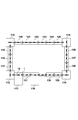
- 1 is a plan view of a vacuum processing apparatus according to a first embodiment of the present invention.
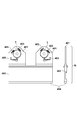
- 1 is a schematic view of a ta-C film forming chamber according to a first embodiment of the present invention. It is the schematic of the conveyance carrier which concerns on 1st Embodiment of this invention.
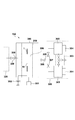
- 1 is a top view of a surface treatment apparatus according to a first embodiment of the present invention. It is a side view of the unload chamber which concerns on 2nd Embodiment of this invention. It is a top view of the vacuum processing apparatus which concerns on 3rd Embodiment of this invention. It is sectional drawing of the film
- FIG. 1 is a plan view showing a vacuum processing apparatus according to this embodiment.
- the vacuum processing apparatus of this embodiment is an in-line film forming apparatus.
- a plurality of chambers 111 to 131 are connected in a rectangular endless shape.
- Each of the chambers 111 to 131 is a vacuum vessel that is evacuated by a dedicated or dual-purpose exhaust system.
- Each chamber is integrally configured with a transfer device capable of transferring between adjacent chambers in a state where the substrate is mounted on the carrier 10.
- the chambers 111 to 131 are connected endlessly through gate valves. Each of the connected chambers 111 to 131 is provided with a transport device that can transport the carrier 10 via a gate valve.
- the transport device has a transport path for transporting the carrier 10 in a vertical posture.
- substrate 1 is mounted in the carrier 10 and is conveyed along the conveyance path not shown.
- the chamber 111 is a load lock chamber for mounting the substrate 1 on the carrier 10.
- the chamber 116 is an unload lock chamber that collects the substrate 1 from the carrier 10.
- the substrate 1 is a metal or glass disk-shaped member having an opening (inner peripheral hole) at the center, and is suitable for use as a magnetic recording medium.
- the substrate processing procedure in the film forming apparatus will be described.
- two unprocessed substrates 1 in the load lock chamber 111 are mounted on the first carrier 10.
- the carrier 10 moves to the adhesion layer forming chamber 117, and an adhesion layer is formed on the substrate 1.
- the operation of mounting the two unprocessed substrates 1 on the next carrier 10 is performed.
- the next carrier 10 moves to the adhesion layer forming chamber 117, an adhesion layer is formed on the substrate 1, and the operation of mounting the substrate 1 on the next carrier 10 is performed in the load lock chamber 111.
- each carrier 10 sequentially performs a predetermined process while moving the chambers 117 to 131 one by one.
- Chambers 117 to 131 are processing chambers for performing various processes.
- the processing chamber include an adhesion layer forming chamber 117 for forming an adhesion layer on the substrate 1, soft magnetic layer formation chambers 118, 119 and 120 for forming a soft magnetic layer on the substrate 1 on which the adhesion layer is formed, soft magnetism.
- a radical processing chamber 130 may be mentioned.
- the chambers 112, 113, 114, and 115 located at the four corners of the vacuum processing apparatus connected in a rectangular closed loop shape change direction with a direction changing device that changes the transport direction of the substrate 1 by 90 degrees.
- the chamber 131 is an ashing processing chamber for removing deposits attached to the carrier.
- Other processing chambers not described above may be configured as a substrate cooling chamber for cooling the substrate 1, a substrate transfer chamber for changing the substrate 1, or the like.
- the ta-C film forming chamber 129 of this embodiment includes a process chamber 201, a filter unit 210 connected so as to communicate with the inside of the process chamber 201, and a source unit 220 connected so as to communicate with the filter unit 210 inside.
- a transfer device 202 that can move the carrier 10 on which the substrate 1 is mounted to a predetermined position is provided.
- the filter unit 210 is a passage for transporting electrons and carbon ions toward the substrate 1, and a magnetic field forming unit such as a filter coil 212 and a permanent magnet is provided so as to surround the filter unit 210.
- the magnetic field forming means forms a magnetic field for transporting electrons and ions.
- the magnetic field forming means of the present embodiment is provided on the outside (atmosphere side) of the filter unit 210, but can also be arranged on the inside (vacuum side).
- the source unit 220 includes a cathode target unit 240 for generating electrons and carbon ions, and an anode anode unit 230 including an anode electrode.
- the arc discharge is maintained by maintaining the electron current or ion current between the anode anode part 230 and the cathode target part 240.
- a carbon target is mounted on the cathode target portion 240 of the present embodiment.
- the ta-C film is formed by an apparatus using vacuum arc discharge, but the ta-C film may be formed by a sputtering process.
- Fig. 3 shows the outline of the carrier.
- the carrier 10 can carry two substrates 1 at the same time.
- the carrier 10 includes two metal holders 401 that hold the substrate 1 and a slider 402 that supports the holder 401 and moves on the conveyance path. Since a plurality of elastic members (plate springs) 403 provided on the holder 401 can support several locations on the outer peripheral portion of the substrate 1, the substrate 1 can be held in a posture facing the target without blocking the front and back film-forming surfaces of the substrate 1.
- the conveying device includes a number of driven rollers arranged along the conveying path and a magnetic screw for introducing power to the vacuum side by a magnetic coupling method.
- the slider 402 of the carrier 10 is provided with a permanent magnet 404.
- the magnetic screw is rotated in a state where the helical magnetic field of the rotating magnetic screw is magnetically coupled to the permanent magnet 404 of the slider 402, the slider 402 (carrier 10) can be moved along the driven roller.
- the configurations disclosed in Japanese Patent Laid-Open No. 8-274142 can be adopted as the configurations of the carrier 10 and the transport apparatus.
- a conveyance device using a linear motor or a rack and pinion may be used.
- a chamber such as the radical processing chamber 130 includes a voltage applying means for changing the potential of the substrate 1.
- the substrate 1 held by the holder of the carrier 10 is electrically connected to the holder 401 via a conductive elastic member (leaf spring) 403.
- the potential of the substrate 1 can be changed by changing the potential of the elastic member 403.
- the voltage applying means is a device for bringing the electrode connected to the substrate voltage applying power supply 302 or the ground into contact with the holder 401.
- the holder 401 may be at ground potential.
- Various electric powers may be applied to the holder 401 using a power source appropriately selected from a DC power source, a pulse power source, a high frequency power source, and the like.
- FIG. 4 is a schematic view of the radical treatment apparatus 130 (surface treatment apparatus) as viewed from above.
- the radical processing apparatus 130 of this embodiment is demonstrated using FIG.
- the radical processing apparatus 130 includes a substrate processing chamber 300 (radical processing container), a radical source 320, a radical introduction path 309 (radical introduction unit) that connects the substrate processing chamber 300 and the radical source 320 between the substrate processing chamber 300 and the radical source 320.
- the radical introduction path 309 includes a flow rate adjustment unit 308 that adjusts the radical flow rate to the substrate processing chamber 300.
- the substrate processing chamber 300 has a symmetrical configuration with respect to the carrier 10 (substrate 1), and a radical source 320 and a radical introduction path 309 are also provided on the left and right, respectively.
- FIG. A transfer device is provided so that the substrate 1 can be held at a predetermined position in the center via the carrier 10.
- the exhaust system 301 is a vacuum pump such as a turbo molecular pump that can evacuate the inside of the substrate processing chamber 300.
- the radical source 320 includes a gas introduction unit 303 that introduces a process gas, a radical generation unit 304 that generates radicals, a radical generation unit 305 that generates power by supplying power to the radical generation unit 304, and a radical generation unit 305. And a valve 307 for controlling the inflow of radicals from the radical generation unit 305 to the radical introduction path 309. The generated radicals are introduced through the radical introduction path 309 and introduced into the substrate processing chamber 300.
- the gas introduction unit 303 includes a gas supply source such as a gas cylinder, a mass flow controller (MFC) that controls the amount of gas introduced from the gas supply source, a gas introduction member that introduces gas into the vacuum vessel, and a space between these members. And has a gas pipe for circulating gas.
- the radical generating means 304 is means for generating radicals.
- the radical generator 305 includes a radical generator 304, and generates radicals by supplying power to the introduced process gas.
- the radical generator 305 is connected to the substrate processing chamber 300 via a radical introduction path 309, and radicals can be introduced into the substrate processing chamber 300 via the radical introduction path 309.
- the radical introduction path 309 is provided with a flow rate adjusting unit 308 configured by an MFC, an orifice, or the like that adjusts the gas flow rate.
- the gas rectifying plate 310 is a pair of plate-like members provided in parallel to the substrate 1 disposed at a predetermined position in the substrate processing chamber 300, and uniformly irradiates the film forming surface of the substrate 1 with radicals. In order to do so, it has a number of gas outlets.
- the gas rectifying plate 310 according to the present embodiment is a gas rectifying plate that is provided with gas ejection ports at equal intervals or opposed to the inner surface of the substrate inner hole, but the gas rectifying plate 310 is annularly arranged with gas ejection ports arranged at equal intervals. It may have. Further, the gas rectifying plates 310 are not limited to a pair and may be provided by one or three or more.
- the substrate processing unit 306 is a space between the gas rectifying plate 310 and the substrate 1 in the substrate processing chamber 300.
- the surface layer of the ta-C film formed on the surface of the substrate 1 is processed (radical processing) by radicals introduced through the gas rectifying plate 310.
- Radical generation means 304 is means for generating plasma using ultraviolet light excitation or plasma excitation.
- the ultraviolet light excitation source for example, an excimer lamp or a xenon lamp is used.
- any plasma source such as a high-frequency plasma or a direct-current plasma source is applicable.
- the radical generating means 304 may be configured by using both ultraviolet light excitation and plasma excitation.
- the radical processing chamber 130 includes a plurality of radical generators 305.
- the radicals may be supplied simultaneously from the plurality of radical generators 305, or the radicals may be supplied alternately one by one.
- the process gas is introduced into the radical generation unit 305 of the radical processing apparatus 130 through the gas introduction unit 303 at a predetermined flow rate.
- oxygen gas O 2 gas
- hydrogen gas H 2 gas
- a mixed gas containing them can be used.
- nitrogen or a mixed gas in which at least one of NO, N 2 O, and NH 3 is mixed, CF 4 , C 2 F 6 , C 3 F 8, or the like can be used as the process gas.
- Desired power is supplied to the radical generating means 304, and the process gas introduced into the radical generating unit 305 is dissociated and excited to generate radicals in the radical generating unit 305.
- the generated radical passes through the radical introduction path 309 together with the introduction gas, and is introduced into the substrate processing unit 306 where the substrate 1 is disposed.
- the flow rate is adjusted to a desired flow rate by the flow rate adjustment unit 308 provided in the radical introduction path 309.
- the radical adjusted to a predetermined flow rate is introduced into the substrate processing chamber 300.
- radicals are irradiated onto the substrate 1 transported to a predetermined position of the substrate processing unit 306 and react with the surface layer of the ta-C film to perform radical processing.
- the radical-treated substrate is discharged from the radical treatment apparatus 130.
- the in-line type vacuum processing apparatus when there is a pressure difference between adjacent processing chambers when the substrate 1 is transported, a chamber having a high pressure when the gate valve is opened. Gas flows into the lower processing chamber. Since the ta-C film forming process of the present invention does not use a process gas, the pressure of the ta-C film forming chamber 129 is lower than that of the adjacent chamber, and there is a possibility that gas flows in from the adjacent chamber. When the ta-C film forming process is performed in a state where the gas from the adjacent chamber remains in the ta-C film forming chamber 129, gas components are mixed into the film, and a desired film quality cannot be obtained.
- carrier transport is performed after sufficiently exhausting the process gas in the processing chamber adjacent to the ta-C film forming chamber 129, or after the gas flowing into the ta-C film forming chamber 129 is sufficiently exhausted, the ta-C film It is desirable to perform the formation.
- the radical processing apparatus 130 since the radical generating unit 305 and the substrate processing unit 306 are separated, an increase in the pressure of the substrate processing unit 306 more than necessary can be suppressed. This is because the radical generating unit 305 and the substrate processing unit 306 are separated, so that gas (radical) adjusted to a predetermined flow rate is introduced into the substrate processing chamber 300, and the amount of gas introduced is reduced. By adopting such a structure, it is possible to further reduce the inflow of the process gas from the radical processing apparatus 130 to the ta-C film forming chamber 129 when the substrate 1 is transported.
- the radical processing may be performed in an unload chamber.
- a configuration example in which radical processing is performed in an unload chamber will be described below as a second embodiment.
- the radical processing performed in the radical processing apparatus 130 of the first embodiment is performed in the unload chamber 516.
- the vacuum processing apparatus of this embodiment replaces the unload chamber 116 of the first embodiment with an unload chamber 516 capable of surface treatment, and does not include the radical processing apparatus 130.
- different processing is performed at the position of the radical processing apparatus 130.
- the unload chamber 516a of the present embodiment corresponds to the radical processing chamber 300 of the first embodiment.
- the same components as those in the first embodiment are denoted by the same reference numerals, and detailed description thereof is omitted.
- the radical processing apparatus is configured integrally with the unload chamber 516.
- the unload chamber and the radical processing apparatus are provided. It also includes adjacent configurations.
- the configuration in which the radical processing apparatus is attached to the substrate discharge side of the unload chamber is the same as that of the unload chamber 516, and the same effect as this embodiment can be expected.
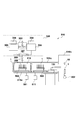
- FIG. 5 is a side view of the unload chamber 516 of the present embodiment.
- the unload chamber 516 includes an unload chamber 516b that removes the substrate 1 from the carrier 10, an unload chamber 516c that accommodates the removed substrate, and an unload chamber that unloads the substrate 1 to the atmosphere after performing surface treatment on the substrate 1. It is comprised from the load chamber 516a.
- the unload chamber 516a and the unload chamber 516c are connected via a gate valve.
- the exhaust devices 501 and 511 are connected to an unload chamber 516a and an unload chamber 516c, respectively.
- Each of the unload chamber 516a and the unload chamber 516c includes a cassette 502 (substrate storage member) that can store a plurality of substrates 1.
- the exhaust devices 501 and 511 include vacuum pumps such as turbo molecular pumps.
- the unload chamber 516a is connected to the radical source 320 via the flow rate adjustment unit 308.
- the radical source 320 was transported to a predetermined position, a gas introduction unit 303 for introducing process gas, a radical generation unit 304 for generating radicals, a radical generation unit 305 for generating radicals by supplying power to the radical generation unit 304
- a substrate processing unit 306 that performs radical processing on the substrate 1, a radical introduction path (radical introduction unit) that introduces radicals generated from the radical generation unit 305 into the substrate processing unit 306, and the inflow of radicals from the radical generation unit 305 to the radical introduction path.
- a valve 307 to be controlled is provided.
- the flow rate adjusting unit 308 is a member that adjusts the flow rate of radicals introduced from the radical source 320 into the unload chamber 516a. That is, a combination of the unload chamber 516a, the flow rate adjustment unit 308, and the radical source 320 of the present embodiment corresponds to the radical processing apparatus 130 of the first embodiment.
- the gas introduction unit 303 is a gas supply source such as a gas cylinder, an MFC that controls the amount of gas introduced from the gas supply source, a gas introduction member that introduces gas into the vacuum vessel, and a gas between these members A gas pipe is provided.
- the gas rectifying plate 510 is a plate-like member provided above the substrate 1 housed in the cassette 502 in the unload chamber 516a, and in order to introduce gas (radicals) uniformly, similar to the gas rectifying plate 310. It has a number of gas outlets. In the present embodiment, only one gas rectifying plate 510 is provided, but a plurality of gas rectifying plates 510 may be provided.
- radical processing of a predetermined number of substrates 1 stored in the cassette 502 can be performed simultaneously.
- radical processing of a large number of substrates 1 can be performed at the same time, so that the throughput can be greatly improved.
- FIG. 6 is a plan view showing a vacuum processing apparatus according to the third embodiment of the present invention.
- the vacuum processing apparatus according to this embodiment is different from the vacuum processing apparatus of the second embodiment in that the ta-C film forming chamber 129 is disposed between the direction changing chamber 115 and the unload chamber 516b. .
- the radical treatment is performed in the unload chamber 516a as in the second embodiment.
- the same components as those in the first embodiment are denoted by the same reference numerals, and detailed description thereof is omitted.
- the substrate 1 on which the ta-C film is formed in the ta-C film forming chamber 129 is transported to the unload chamber 516b, the substrate 1 is removed from the carrier 10, and stored in the cassette 502. Thereafter, when a plurality of sheets are stored in the cassette 502, the substrate is transferred from the unload chamber 516b to the unload chamber 516a by the substrate transfer robot 151, and is used on both surfaces of the substrate 1 by using the unload chamber shown in FIG. Perform radical treatment using radicals.
- the ta-C film forming chamber 129 is disposed between the direction changing chamber 115 and the unload chamber 516b as a radical processing apparatus, and the surface treatment (radical processing) is performed in the unload chamber. It was set as the structure performed by 516a. For this reason, chambers using process gas are not arranged on both sides of the ta-C film forming chamber 129. With such an arrangement, in an in-line manufacturing apparatus, it is possible to reliably prevent the flow of process gas from the adjacent chamber to the ta-C film forming chamber 129 when the substrate 1 is transported, and to produce a ta-C film with good film quality. It can be formed continuously with high productivity.
- Examples of surface treatment using the above-described vacuum processing apparatus will be described below as Examples 1 and 2.
- a ta-C film was sequentially laminated on a substrate as an adhesion layer, a lower soft magnetic layer, a seed layer, an intermediate layer, a magnetic recording layer, and a surface protective layer.
- the substrate was transported to the radical processing apparatus 130, and surface treatment using radicals was performed on both surfaces of the substrate on which the ta-C film was formed.
- the vacuum processing apparatus of 2nd Embodiment or 3rd Embodiment the same process is performed except performing a radical process in the unload chamber 516a.
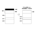
- FIG. 7 illustrates a surface treatment method according to the first embodiment.
- a layer 603 having a low sp 3 bond ratio is generated in the vicinity of the surface to a depth of about 0.5 nm.
- the layer 603 with a low sp 3 bond ratio is removed without increasing the surface roughness, and the layer with a high sp 3 bond ratio is removed. 602 remains, and the sp 3 bond ratio in the entire film increases.
- a layer 611 between the substrate cross section 612 and the magnetic layer 610 is a laminate of an adhesion layer, a soft magnetic layer, a seed layer, and an intermediate layer.
- the material of the adhesion layer AlTi, AlTa, NiTa, CoTiAl, or the like can be used.
- the material of the soft magnetic layer a laminate of FeCo alloy, FeTa alloy, Co alloy, etc. and Ru alloy, etc. can be used.
- As a material for the seed layer NiW alloy, NiFe alloy, NiTa alloy, TaTi alloy or the like can be used.
- a laminate of Ru or Ru alloy can be used for the intermediate layer.
- the radical in the outermost layer of sp 3 bond ratio is higher layers 602 in sp 3 bond ratio is lower layers 603 are removed by the radicals are irradiated, the uppermost layer of the surface of the sp 3 bond ratio is higher layers 602 Energy can be controlled uniformly.
- the radical generating unit 305 is connected to the substrate processing unit 306 via the radical introduction path 309, and the ta-C film is not directly exposed to plasma or ultraviolet light. Therefore, there is no damage to the ta-C film caused by ions or ultraviolet light having kinetic energy flying from the plasma during the surface treatment, so that the ta-C film is not altered and the characteristics are not impaired.
- oxygen gas, hydrogen gas, or a mixed gas containing them can be used as the process gas in this embodiment.
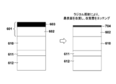
- FIG. 8 illustrates a surface treatment method according to the second embodiment.
- the layer 603 having a low sp 3 bond ratio is formed on the surface where the ta-C film 601 is formed.
- the surface treatment layer 704 in which the layer 603 having a low sp 3 bond ratio was modified by radical irradiation was formed.
- radical irradiation in this embodiment, etching is performed while the surface treatment layer 704 is formed, so that the surface treatment layer 704 thinner than the layer 603 having a low sp 3 bond ratio can be formed.
- Surface treatment layer 704 is a layer sp 3 bonds the ratio of the surface was modified low layer 603, the surface roughness in comparison sp 3 bond ratio is low layer 603 does not increase.
- the characteristics and etching rate of the surface treatment layer 704 formed in Example 2 can be controlled by selecting the amount of radicals to be irradiated, the irradiation time, the mixing ratio of process gases, and the like.
- the surface treatment layer 704 can be provided with characteristics that improve hydrophilicity and lubricant adsorption by forming a nitride layer, or characteristics that improve water repellency and releasability by forming a fluoride layer.
- a gas species that generates radicals is selected in accordance with the imparted characteristics and supplied to the radical generator 305.
- a nitride layer is formed as the surface treatment layer 704
- nitrogen or a mixed gas in which at least one of NO, N 2 O, and NH 3 is mixed is used as a process gas.
- the characteristics and etching rate of the surface treatment layer can be controlled by selecting the amount of radicals to be irradiated, the irradiation time, the mixing ratio of process gases, and the like.
- CF 4 , C 2 F 6 , C 3 F 8 or the like is used as a process gas.
- the characteristics and etching rate of the surface treatment layer can be controlled by selecting the amount of radicals to be irradiated, the irradiation time, and the gas type. Desired power is supplied to the radical generating means 304, and the process gas introduced into the radical generating unit 305 is dissociated and excited to generate radicals in the radical generating unit 305.
- both modification for example, nitriding
- etching of the extreme surface layer can be performed at the same time.
- the selected gas type for example, pure N 2
- only modification of the extreme surface is possible. It can also be set as the process which performs.
Landscapes
- Chemical & Material Sciences (AREA)
- Engineering & Computer Science (AREA)
- Organic Chemistry (AREA)
- Materials Engineering (AREA)
- Mechanical Engineering (AREA)
- Metallurgy (AREA)
- Chemical Kinetics & Catalysis (AREA)
- Physics & Mathematics (AREA)
- Plasma & Fusion (AREA)
- Analytical Chemistry (AREA)
- Physical Vapour Deposition (AREA)
- Chemical Vapour Deposition (AREA)
- Manufacturing Of Magnetic Record Carriers (AREA)
Abstract
基板上に形成された前記磁気記録層を保護する表面保護層を有する磁気記録媒体の真空処理方法は、磁気記録層の上にta-C膜を形成するta-C膜形成工程と、ta-C膜が形成された基板を搬送する搬送工程と、プロセスガスを励起してラジカルを発生させるラジカル発生工程と、ta-C膜の表面に前記ラジカルを照射するラジカル処理工程とを有する。
Description
本発明は、表面保護層の処理に適した真空処理装置、及び表面保護層の真空処理方法に係り、特に磁気記録媒体の表面保護層の真空処理方法及び表面保護層の処理に適した真空処理装置に関する。
ハードディスクドライブの磁気記録媒体の表層には、磁気記録層を保護するための表面保護層が形成されている。表面保護層にはDLC(ダイヤモンドライクカーボン)が好適とされ、スパッタリング法や化学的気相成長法(CVD法)で形成された保護層が適用されている。磁気記録層と磁気ヘッドの磁気的隙間の狭小化により、記録密度を増大させることができるため、表面保護層の薄膜化が必要となる。そのため、極薄膜でも耐久性が満足できる保護膜が要求されており、表面保護層として、従来よりも耐久性および耐食性に優れたta-C(テトラヘドラル・アモルファスカーボン)膜を用いることが検討されている。ta-C膜は炭素イオンによる物理的蒸着法で成膜される。例えば、特許文献1に示すような真空アーク成膜装置が用いられる。
真空アーク成膜装置により形成されたta-C膜の最表面には、sp3結合比率が低く、硬さの低い層が生じることが知られている。表面保護層を薄くすると、膜全体の厚さに占める硬さの低い層の厚さの割合が高くなるので、ta-C膜本来の特性が損なわれる。表面保護層をさらに薄くするためには、表面のsp3結合比率が低い層を除去することが望ましい。例えば特許文献2には、保護層を薄くするために、イオンビームを用いて表層を除去する技術が開示されている。
磁気記録媒体の製造工程では、表面保護層形成後にフルオロカーボン系液体潤滑剤が塗布されているが、特許文献1の技術は、処理後の基板表面に存在するダングリングボンドにより表面エネルギが均一になりにくい。そのため潤滑剤塗布後の表面状態の均一性が十分でない。また、ハードディスクドライブの記録密度の増加には表面を平坦にすることが望ましいが、アルゴンイオンを用いてエッチングを行うと、基板の表面粗さが増加する傾向がある。
本発明の目的は、真空アーク成膜装置により形成されたta-C膜の最表層を最適化する表面処理方法、および、このような表面処理に適した真空処理装置を提供することにある。本発明の他の目的は、処理後の基板の表面が平坦にできる表面処理方法、および、このような表面処理に適した真空処理装置を提供することにある。
本発明に係る真空処理装置は、基板にta-C膜からなる表面保護層を形成するta-C膜形成装置と、前記表面保護層にラジカルを反応させるラジカル処理を行うラジカル処理装置と、前記基板を大気に曝すことなく前記ta-C膜形成装置から前記ラジカル処理装置に搬送する搬送装置と、を備えることを特徴とする。
或いは、本発明に係る真空処理方法は、基板上に形成された前記磁気記録層を保護する表面保護層を有する磁気記録媒体の真空処理方法であって、前記磁気記録層の上にta-C膜を形成するta-C膜形成工程と、前記ta-C膜が形成された基板を搬送する搬送工程と、プロセスガスを励起してラジカルを発生させるラジカル発生工程と、前記ta-C膜の表面に前記ラジカルを照射するラジカル処理工程と、を有することを特徴とする。
本発明の表面処理方法によれば、表面保護層本来の特性を損なわずに、sp3結合比率が低い層を除去できる。また、表面処理後の表面の化学的性質を望ましいものにすることができる。あるいは、本発明の表面処理方法によれば表面に新たな機能を付与することができる。本発明の表面処理方法はラジカルを用いて化学的にエッチングするため、表層の除去による表面粗さの増加を防ぐことができる。本発明の方法の実施の際には必ずしも基板ステージを回転させる必要がないため安価な装置を使用することができる。本発明の方法をインライン製造装置で実施する場合は、基板搬送時のラジカル処理装置からta-C室へのガス流入によるクロスコンタミネーションを低減できる。
本発明のその他の特徴及び利点は、添付図面を参照とした以下の説明により明らかになるであろう。なお、添付図面においては、同じ若しくは同様の構成には、同じ参照番号を付す。
添付図面は明細書に含まれ、その一部を構成し、本発明の実施の形態を示し、その記述と共に本発明の原理を説明するために用いられる。
本願発明の第1実施形態に係る真空処理装置の平面図である。
本願発明の第1実施形態に係るta-C膜形成室の概略図である。
本願発明の第1実施形態に係る搬送キャリアの概略図である。
本願発明の第1実施形態に係る表面処理装置の上面図である。
本願発明の第2実施形態に係るアンロードチャンバの側面図である
本願発明の第3実施形態に係る真空処理装置の平面図である。
本願発明の第1実施例の表面処理方法によって作製した膜の断面図である。
本願発明の第2実施例の表面処理方法によって作製した膜の断面図である。
以下、図面を参照して、本発明の好適な実施形態を詳しく説明する。ただし、この実施の形態に記載されている構成要素はあくまで例示である。本発明の技術的範囲は、特許請求の範囲によって確定されるのであって、以下の個別の実施形態によって限定されるわけではない。以下に、本発明の成膜装置を、真空アーク成膜法(Vacuum Arc Deposition)を用いて被処理物としての基板に保護層を形成する成膜装置に適用した実施形態について説明する。
(第1実施形態)
まず、本発明に用いる真空処理装置について図1乃至4を用いて説明する。図1は本実施形態に係る真空処理装置を示す平面図である。本実施形態の真空処理装置はインライン式の成膜装置である。本実施形態の真空処理装置は、複数のチャンバ111~131が矩形の無端状に連結されている。各チャンバ111~131は専用又は兼用の排気系によって排気される真空容器である。それぞれのチャンバには、キャリア10に基板が搭載された状態で、隣り合うチャンバ間で搬送できる搬送装置が一体に構成されている。
まず、本発明に用いる真空処理装置について図1乃至4を用いて説明する。図1は本実施形態に係る真空処理装置を示す平面図である。本実施形態の真空処理装置はインライン式の成膜装置である。本実施形態の真空処理装置は、複数のチャンバ111~131が矩形の無端状に連結されている。各チャンバ111~131は専用又は兼用の排気系によって排気される真空容器である。それぞれのチャンバには、キャリア10に基板が搭載された状態で、隣り合うチャンバ間で搬送できる搬送装置が一体に構成されている。
各チャンバ111~131はゲートバルブを介して無端状に連結されている。連結された各チャンバ111~131にはゲートバルブを介してキャリア10を搬送できる搬送装置が設けられている。搬送装置は、キャリア10を垂直姿勢で搬送する搬送路を有している。基板1は、キャリア10に搭載されて不図示の搬送路に沿って搬送されるようになっている。チャンバ111は、キャリア10への基板1の搭載を行うロードロック室である。チャンバ116は、キャリア10からの基板1の回収を行うアンロードロック室である。なお、基板1は中心部分に開口(内周孔部)を有する金属製、若しくはガラス製の円板状部材であり、磁気記録媒体としての使用に適したものである。
成膜装置内での基板の処理手順について説明する。まず、ロードロックチャンバ111内で未処理の2枚の基板1が最初のキャリア10に搭載される。このキャリア10は密着層形成室117に移動して、基板1に密着層が形成される。最初のキャリア10が密着層形成室117に配置されているときに、次のキャリア10へ、2枚の未処理の基板1の搭載動作が行われる。その後、次のキャリア10は密着層形成室117に移動し、基板1に密着層が形成され、ロードロックチャンバ111内でさらに次のキャリア10への基板1の搭載動作が行われる。1タクトタイムが経過する毎に、各キャリア10はチャンバ117~131を1ずつ移動しながら、順次所定の処理がなされる。
チャンバ117~131は各種処理を行う処理室である。処理室の具体例としては、基板1に密着層を形成する密着層形成室117、密着層が形成された基板1に軟磁性層を形成する軟磁性層形成室118、119、120、軟磁性層の形成された基板1にシード層を形成するシード層形成室121、シード層が形成された基板1に中間層を形成する中間層形成室123、124、中間層が形成された基板1に磁性膜を形成する磁性膜形成室126、127、128、磁性膜の上にta-C膜からなる表面保護層を形成するta-C膜形成チャンバ129、ta-C膜の表面をラジカル処理するラジカル処理チャンバ130(ラジカル処理装置)が挙げられる。また、矩形の閉ループ状に接続された真空処理装置の4つの角の部分に位置するチャンバ112、113、114、115は、基板1の搬送方向を90度転換する方向転換装置を備えた方向転換チャンバである。チャンバ131はキャリアに付着した堆積物を除去するアッシング処理室である。上述しなかった他の処理室は、基板1を冷却する基板冷却室や、基板1を持ち替える基板持替室などとして構成されうる。
ta-C膜形成チャンバ129の概略図を図2に示す。図2を用いて本実施形態のta-C膜形成チャンバ129について説明する。ta-C膜形成チャンバ129は、プロセスチャンバ201と、プロセスチャンバ201と内部が連通するように連結されたフィルタ部210と、フィルタ部210に内部で連通されるように連結されたソース部220を有する。プロセスチャンバ201内には、基板1を搭載したキャリア10を所定位置に移動できる搬送装置202が設けられている。
フィルタ部210は電子及びカーボンイオンを基板1に向けて輸送する通路であり、フィルタ部210を囲むようにフィルタコイル212や永久磁石等の磁場形成手段が設けられている。磁場形成手段は電子、およびイオンを輸送するための磁場を形成する。本実施形態の磁場形成手段は、フィルタ部210の外側(大気側)に設けられているが内部(真空側)にも配置されうる。
ソース部220は、電子及びカーボンイオンを生成するための陰極ターゲット部240と、アノード電極を備える陽極アノード部230を有している。陽極アノード部230と陰極ターゲット部240間での電子電流もしくはイオン電流を維持することにより、アーク放電を維持する。本実施形態の陰極ターゲット部240にはカーボン製のターゲットが搭載される。また、本実施形態ではta-C膜を真空アーク放電を用いた装置で形成したがta-C膜はスパッタリングプロセスで形成してもよい。
図3にキャリアの概略を示す。キャリア10は2枚の基板1を同時に搭載することができる。キャリア10は、基板1を保持する金属製のホルダー401を2つと、ホルダー401を支持して搬送路上を移動するスライダ402とを有している。ホルダー401に設けられた複数の弾性部材(板ばね)403で基板1の外周部の数カ所を支持できるため、基板1の表裏の成膜面を遮ることなくターゲットに対向した姿勢で保持できる。
搬送装置は、搬送路に沿って並べられた多数の従動ローラと、磁気結合方式により動力を真空側に導入する磁気ネジを備えている。キャリア10のスライダ402は永久磁石404が設けられている。回転する磁気ネジのらせん状の磁場をスライダ402の永久磁石404と磁気結合させた状態で、磁気ねじを回転させるとスライダ402(キャリア10)を従動ローラに沿って移動させることができる。なお、キャリア10及び搬送装置の構成としては特開平8-274142号公報に開示された構成を採用しうる。もちろん、リニアモータやラックアンドピニオンを用いた搬送装置を用いてもよい。
ラジカル処理チャンバ130などのチャンバは、基板1の電位を変更する電圧印加手段を備えている。キャリア10のホルダーに保持された基板1は、導電性の弾性部材(板ばね)403を介してホルダー401と電気的に接続されている。弾性部材403の電位を変更することで基板1の電位を変更することができる。電圧印加手段は、基板電圧印加電源302若しくはアースに接続された電極をホルダー401に接触させる装置である。ホルダー401は接地電位でもよい。また、ホルダー401に、直流電源、パルス電源または高周波電源などから適宜選択した電源を用いて各種の電力を印加してもよい。
図4はラジカル処理装置130(表面処理装置)を上方から見た模式図である。図4を用いて本実施形態のラジカル処理装置130について説明する。ラジカル処理装置130は、基板処理チャンバ300(ラジカル処理容器)、ラジカル源320、基板処理チャンバ300とラジカル源320の間に基板処理チャンバ300とラジカル源320を連結するラジカル導入路309(ラジカル導入部)を備えている。ラジカル導入路309は基板処理チャンバ300へのラジカル流量を調整する流量調整部308を有する。基板処理チャンバ300は、キャリア10(基板1)を基準として左右対称の構成を備えており、ラジカル源320とラジカル導入路309も左右にそれぞれ設けられている。そのため、キャリア10に保持された2つの基板1の両面に同時に処理できる。キャリア10を介して基板1を中央の所定位置に保持できるように搬送装置が設けられている。排気系301は、基板処理チャンバ300内を真空排気できるターボ分子ポンプ等の真空ポンプである。
ラジカル源320は、プロセスガスを導入するガス導入部303と、ラジカルを生成するラジカル発生手段304と、ラジカル発生手段304に電力を投入してラジカルを発生するラジカル発生部305と、ラジカル発生部305とラジカル発生部305からラジカル導入路309へのラジカルの流入を制御するバルブ307を備えている。発生したラジカルがラジカル導入路309を通って導入され、基板処理チャンバ300に導入される。
ガス導入部303は、ガスボンベ等のガス供給源、ガス供給源から供給されるガス導入量をコントロールするマスフローコントローラ(MFC)、真空容器内にガスを導入するガス導入部材、及びこれらの部材の間でガスを流通させるガス管を有している。ラジカル発生手段304はラジカルを生成する手段である。ラジカル発生部305はラジカル発生手段304を備えたものであり、導入されたプロセスガスに電力を投入してラジカルを発生する。ラジカル発生部305はラジカル導入路309を介して基板処理チャンバ300に接続され、ラジカル導入路309を介してラジカルを基板処理チャンバ300内に導入できる。ラジカル導入路309にはガス流量を調整するMFCやオリフィスなどから構成された流量調整部308が設けられている。
ガス整流板310は、基板処理チャンバ300内で所定位置に配置された基板1に対して平行に設けられた一対の板状部材であり、ラジカルを基板1の成膜面に対して均一に照射するために多数のガス噴き出し口を有している。本実施形態のガス整流板310は、均等間隔若しくは基板内孔の対向面にガス噴き出し口が設けられたものを用いたが、ガス整流板310は、環状に均等間隔に配置されたガス噴き出し口を有するものでもよい。また、ガス整流板310は一対に限らず、1枚、もしくは3枚以上設けてもよい。基板処理部306は、基板処理チャンバ300内において、ガス整流板310と基板1の間の空間である。基板処理部306内で、ガス整流板310を介して導入されたラジカルにより基板1の表面に形成されたta-C膜の表層に処理(ラジカル処理)がされる。
ラジカル発生手段304は、紫外光励起もしくはプラズマ励起を用いてプラズマを生成する手段である。紫外光励起源としては、例えば、エキシマランプ、キセノンランプが用いられる。プラズマ励起を用いた場合、高周波プラズマ、直流プラズマ源のいかなるプラズマ源も適用可能である。紫外光励起とプラズマ励起を併用してラジカル発生手段304を構成してもよい。
ラジカル処理チャンバ130はラジカル発生部305を複数備えている。複数のラジカル発生部305から同時にラジカルを供給してもよいし、1つずつ交互にラジカルを供給するようにしてもよい。交互にラジカルを供給する場合は、1タクトタイム終了後に、次の基板処理に対して直前のプロセスで使用していないラジカル発生部305から基板処理チャンバにラジカルを供給するとよい。こうすると、ラジカルを安定して供給できるため生産性の向上を図れる。
ラジカル処理装置130を使用した表面処理工程について詳細に説明する。プロセスガスをラジカル処理装置130のラジカル発生部305にガス導入部303を介して所定の流量で導入する。プロセスガスとしては、酸素ガス(O2ガス)または水素ガス(H2ガス)もしくはそれらを含んだ混合ガスを用いることができる。あるいは、プロセスガスとして、窒素あるいはNO、N2O、NH3のうち少なくとも1つを混合した混合ガスやCF4、C2F6、C3F8等を用いることもできる。ラジカル発生手段304に所望の電力を投入し、ラジカル発生部305に導入したプロセスガスを解離及び励起してラジカル発生部305にてラジカルを発生させる。
発生したラジカルは、導入ガスと共にラジカル導入路309を通過して、基板1が配置される基板処理部306へ導入される。この導入中、ラジカル導入路309に設けられた流量調整部308により、所望の流量に調整される。所定の流量に調整されたラジカルは、基板処理チャンバ300内に導入される。そして、ラジカルが基板処理部306の所定位置に搬送された基板1に照射されてta-C膜の表層と反応してラジカル処理が行われる。ラジカル処理された基板をラジカル処理装置130から排出する。
なお、本実施形態のようなインライン式の真空処理装置装置(図1参照)では、基板1の搬送時に隣接処理チャンバ間に圧力差がある場合、ゲートバルブを開放したときに、圧力が高いチャンバから低い処理室に向かってガスが流入する。本発明のta-C膜形成プロセスはプロセスガスを使用しないため、ta-C膜形成室129の圧力は隣接室より低く、隣接室からガスが流入するおそれがある。そして、ta-C膜形成室129に隣接室からのガスが残存した状態でta-C膜形成プロセスを行うと膜中にガス成分が混入し、所望の膜質を得ることができない。このため、ta-C膜形成室129に隣接した処理室のプロセスガスを十分排気した後にキャリア搬送を行う、若しくはta-C膜形成室129に流入したガスを十分排気した後にta-C膜の形成を行うことが望ましい。
ラジカル処理装置130は、ラジカル発生部305と基板処理部306が分かれていることから、基板処理部306の圧力の必要以上の上昇を抑えることができる。ラジカル発生部305と基板処理部306が分かれているので、基板処理チャンバ300には所定流量に調整されたガス(ラジカル)導入となり、ガスの導入量が少なくなるためである。このような構造としたことにより、基板1の搬送時にラジカル処理装置130からta-C膜形成チャンバ129へのプロセスガスの流入をさらに低減できる。
(第2実施形態)
上述の第1実施形態ではラジカル処理装置130でラジカル処理を行う構成例について説明したが、ラジカル処理をアンロードチャンバで行ってもよい。ラジカル処理をアンロードチャンバで行う構成例について第2実施形態として以下に説明する。本実施形態は、第1実施形態のラジカル処理装置130で行ったラジカル処理をアンロードチャンバ516内で行う構成である。図1の真空処理装置と比べると、本実施形態の真空処理装置は、第1実施形態のアンロードチャンバ116を表面処理が可能なアンロードチャンバ516に交換し、ラジカル処理装置130を備えない、もしくはラジカル処理装置130の位置で異なる処理を行う構成となる。すなわち、本実施形態のアンロードチャンバ516aは、第1実施形態のラジカル処理チャンバ300に相当する。なお、本実施形態の説明において、第1実施形態と同様の構成については同じ符号を付してその詳細な説明を省略する。
上述の第1実施形態ではラジカル処理装置130でラジカル処理を行う構成例について説明したが、ラジカル処理をアンロードチャンバで行ってもよい。ラジカル処理をアンロードチャンバで行う構成例について第2実施形態として以下に説明する。本実施形態は、第1実施形態のラジカル処理装置130で行ったラジカル処理をアンロードチャンバ516内で行う構成である。図1の真空処理装置と比べると、本実施形態の真空処理装置は、第1実施形態のアンロードチャンバ116を表面処理が可能なアンロードチャンバ516に交換し、ラジカル処理装置130を備えない、もしくはラジカル処理装置130の位置で異なる処理を行う構成となる。すなわち、本実施形態のアンロードチャンバ516aは、第1実施形態のラジカル処理チャンバ300に相当する。なお、本実施形態の説明において、第1実施形態と同様の構成については同じ符号を付してその詳細な説明を省略する。
本実施形態のラジカル処理装置はアンロードチャンバ516と一体に構成されているが、これは、アンロードチャンバ516内にラジカル処理装置を組み込んだ構成の他にも、アンロードチャンバとラジカル処理装置を隣接させた構成も含むものである。例えば、ラジカル処理装置をアンロードチャンバの基板排出側に取り付ける構成はアンロードチャンバ516と同様のものであり、本実施形態と同じ効果が期待できる。
図5は、本実施形態のアンロードチャンバ516の側面図である。アンロードチャンバ516は、基板1をキャリア10から取り外すアンロードチャンバ516bと、取り外した基板を収容するアンロードチャンバ516cと、基板1に表面処理を実施した後、基板1を大気側に搬出するアンロードチャンバ516aから構成されている。アンロードチャンバ516aとアンロードチャンバ516cはゲートバルブを介して接続されている。排気装置501、511はそれぞれアンロードチャンバ516a、アンロードチャンバ516cに接続されている。アンロードチャンバ516a、アンロードチャンバ516cのそれぞれは、基板1を複数収容できるカセット502(基板収納部材)を備えている。排気装置501、511は、ターボ分子ポンプ等の真空ポンプを備えている。
アンロードチャンバ516aは、流量調整部308を介してラジカル源320に接続されている。ラジカル源320は、プロセスガスを導入するガス導入部303と、ラジカルを生成するラジカル発生手段304、ラジカル発生手段304に電力を投入してラジカルを発生するラジカル発生部305、所定位置に搬送された基板1をラジカル処理する基板処理部306、ラジカル発生部305から発生したラジカルを基板処理部306に導入するラジカル導入路(ラジカル導入部)、ラジカル発生部305からラジカル導入路へのラジカルの流入を制御するバルブ307を備えている。また、流量調整部308はラジカル源320からアンロードチャンバ516aに導入されるラジカルの流量を調整する部材である。すなわち、本実施形態のアンロードチャンバ516aと流量調整部308とラジカル源320を合わせたものが、第1実施形態のラジカル処理装置130に相当する。
ガス導入部303は、ガスボンベ等のガス供給源、ガス供給源から供給されるガス導入量をコントロールするMFC、真空容器内にガスを導入するガス導入部材、及びこれらの部材の間でガスを流通させるガス管を有している。ガス整流板510は、アンロードチャンバ516a内のカセット502に収納された基板1の上方に設けられた板状部材であり、ガス整流板310と同様、ガス(ラジカル)を均一に導入するために多数のガス噴き出し口を有している。本実施形態ではガス整流板510を1枚だけ設けているが、複数設けてもよい。
ラジカル導入路309とガス整流板510を介してラジカルを導入することにより、カセット502に収納された所定数の基板1のラジカル処理を同時に行うことができる。本実施形態の真空処理装置によれば、多数の基板1のラジカル処理を同時に行うことができるため、スループットを大幅に向上させることができる。
(第3実施形態)
図6は、本発明の第3実施形態に係る真空処理装置を示す平面図である。本実施形態に係る真空処理装置は、ta-C膜形成室129を、方向転換室115とアンロードチャンバ516bの間に配置されている点で、第2実施形態の真空処理装置と異なっている。ラジカル処理はアンロードチャンバ516aで行うことは第2実施形態と同様である。なお、本実施形態の説明において、第1実施形態と同様の構成については同じ符号を付してその詳細な説明を省略する。
図6は、本発明の第3実施形態に係る真空処理装置を示す平面図である。本実施形態に係る真空処理装置は、ta-C膜形成室129を、方向転換室115とアンロードチャンバ516bの間に配置されている点で、第2実施形態の真空処理装置と異なっている。ラジカル処理はアンロードチャンバ516aで行うことは第2実施形態と同様である。なお、本実施形態の説明において、第1実施形態と同様の構成については同じ符号を付してその詳細な説明を省略する。
本実施形態に係る真空処理装置にてラジカル処理を行う場合について説明する。まず、ta-C膜形成室129でta-C膜が形成された基板1をアンロードチャンバ516bに搬送し、キャリア10から基板1を取り外し、カセット502に収納する。その後、カセット502に複数枚収納された時点で、基板載せ換えロボット151によりアンロードチャンバ516bからアンロードチャンバ516aに搬送し、図5に示したアンロードチャンバを使用して、基板1の両面にラジカルを用いたラジカル処理を行う。
本実施形態に係る真空処理装置では、ta-C膜形成室129を、方向転換室115と、ラジカル処理装置としてのアンロードチャンバ516bの間に配置し、表面処理(ラジカル処理)はアンロードチャンバ516aで行う構成とした。このため、ta-C膜形成室129の両側にプロセスガスを使用するチャンバを配置していない。このような配置とすることで、インライン式の製造装置において、基板1の搬送時に隣接室からta-C膜形成室129へのプロセスガスの流入を確実に防ぎ、膜質のよいta-C膜を高い生産性で連続して形成することができる。
上述した真空処理装置を用いた表面処理の例を実施例1,2として以下に説明する。上述した第1実施形態に示す装置を用いて、基板の上に密着層、下部軟磁性層、シード層、中間層、磁気記録層、表面保護層としてta-C膜を順次積層した。次に、基板をラジカル処理装置130に搬送し、ta-C膜が形成された基板の両面にラジカルを用いた表面処理を実施した。なお、第2実施形態もしくは第3実施形態の真空処理装置を用いる場合は、ラジカル処理をアンロードチャンバ516aで行う以外は同様の処理が行われる。
(実施例1)
図7は、実施例1に係る表面処理方法である。磁性層610上に形成されたta-C膜601の表面には、sp3結合比率が低い層603が表面近傍、深さ0.5nm程度まで生じている。図7に示すようにラジカルで表面保護層601の一部を除去した後は、表面粗さの増加を伴わずに、sp3結合比率が低い層603が除去され、sp3結合比率が高い層602が残り、膜全体に占めるsp3結合比率が高くなる。基板断面612と磁性層610の間の層611は、密着層、軟磁性層、シード層、中間層の積層体である。密着層の材料としては、AlTi、AlTa、NiTa、またはCoTiAl等を用いることができる。軟磁性層の材料としては、FeCo合金、FeTa合金、Co合金等とRu合金等との積層体を用いることができる。シード層の材料としては、NiW合金、NiFe合金、NiTa合金、TaTi合金等を用いることができる。中間層にはRuやRu合金の積層体を用いることができる。
図7は、実施例1に係る表面処理方法である。磁性層610上に形成されたta-C膜601の表面には、sp3結合比率が低い層603が表面近傍、深さ0.5nm程度まで生じている。図7に示すようにラジカルで表面保護層601の一部を除去した後は、表面粗さの増加を伴わずに、sp3結合比率が低い層603が除去され、sp3結合比率が高い層602が残り、膜全体に占めるsp3結合比率が高くなる。基板断面612と磁性層610の間の層611は、密着層、軟磁性層、シード層、中間層の積層体である。密着層の材料としては、AlTi、AlTa、NiTa、またはCoTiAl等を用いることができる。軟磁性層の材料としては、FeCo合金、FeTa合金、Co合金等とRu合金等との積層体を用いることができる。シード層の材料としては、NiW合金、NiFe合金、NiTa合金、TaTi合金等を用いることができる。中間層にはRuやRu合金の積層体を用いることができる。
さらに、sp3結合比率が低い層603がラジカルで除去される際にsp3結合比率が高い層602の最表層にラジカルが照射されるため、sp3結合比率が高い層602の最表層の表面エネルギを均一に制御することができる。本実施形態の表面処理では、ラジカル発生部305が基板処理部306とラジカル導入路309を介して接続されており、ta-C膜が直接プラズマまたは紫外光に曝されることがない。そのため、表面処理時にプラズマから飛来する運動エネルギを有したイオンや紫外光によるta-C膜へのダメージがないため、ta-C膜が変質し特性を損なうことがない。本実施例でのプロセスガスとしては、酸素ガスまたは水素ガスもしくはそれらを含んだ混合ガスを用いることができる。
(実施例2)
図8は、実施例2に係る表面処理方法である。上述のように、ta-C膜601が形成された表面には、sp3結合比率が低い層603が形成されている。本実施例では、ラジカル照射によりsp3結合比率が低い層603を改質した表面処理層704を形成した。本実施例のラジカル照射では、表面処理層704を形成しながらエッチングするため、sp3結合比率が低い層603より薄い表面処理層704を形成できる。表面処理層704は、表面のsp3結合比率が低い層603を改質した層であり、sp3結合比率が低い層603と比べて表面粗さは増加していない。
図8は、実施例2に係る表面処理方法である。上述のように、ta-C膜601が形成された表面には、sp3結合比率が低い層603が形成されている。本実施例では、ラジカル照射によりsp3結合比率が低い層603を改質した表面処理層704を形成した。本実施例のラジカル照射では、表面処理層704を形成しながらエッチングするため、sp3結合比率が低い層603より薄い表面処理層704を形成できる。表面処理層704は、表面のsp3結合比率が低い層603を改質した層であり、sp3結合比率が低い層603と比べて表面粗さは増加していない。
ここで、実施例2で形成した表面処理層704の特性とエッチング速度は、照射するラジカル量、照射時間、プロセスガスの混合比等を選択することで制御できる。例えば、窒化層形成による親水性及び潤滑剤吸着性を改善した特性、あるいはフッ化層形成による撥水性及び離型性を改善した特性を付与した表面処理層704にすることができる。ラジカル処理の際に、付与した特性に合わせてラジカルを生成するガス種を選択して、ラジカル発生部305に供給する。
表面処理層704として窒化層を形成する場合には、プロセスガスとして、窒素あるいはNO、N2O、NH3のうち少なくとも1つを混合した混合ガスが用いられる。ここで、表面処理層の特性とエッチング速度は、照射するラジカル量、照射時間、プロセスガスの混合比等を選択することで制御できる。特に、上記のプロセスガスに加えて酸素もしくは水素ガスを添加することで、カーボンのエッチングを促進することが可能である。
表面処理層704としてフッ化層を形成する場合には、プロセスガスとして、CF4、C2F6、C3F8等が用いられる。ここで、表面処理層の特性とエッチング速度は、照射するラジカル量、照射時間、ガス種を選択することで制御できる。ラジカル発生手段304に所望の電力を投入し、ラジカル発生部305に導入したプロセスガスを解離及び励起してラジカル発生部305にてラジカルを発生させる。実施例2のラジカル処理では、極表層の改質(例えば窒化)とエッチングの両方を同時に行うことができるが、選択されたガス種(例えば、純N2など)によっては極表面の改質だけを行う処理とすることもできる。
本発明は上記実施の形態に制限されるものではなく、本発明の精神及び範囲から離脱することなく、様々な変更及び変形が可能である。従って、本発明の範囲を公にするために、以下の請求項を添付する。
本願は、2014年3月4日提出の日本国特許出願特願2014-41685を基礎として優先権を主張するものであり、その記載内容の全てを、ここに援用する。
Claims (13)
- 基板にta-C膜からなる表面保護層を形成するta-C膜形成装置と、
前記表面保護層にラジカルを反応させるラジカル処理を行うラジカル処理装置と、
前記基板を大気に曝すことなく前記ta-C膜形成装置から前記ラジカル処理装置に搬送する搬送装置と、
を備えることを特徴とする真空処理装置。 - 前記真空処理装置は、前記基板にそれぞれ所定の処理を行う複数のチャンバが矩形の無端状に連結されており、
前記複数のチャンバは、前記基板の搬送方向を転換するために前記矩形の角の位置に配置された方向転換チャンバと、前記ta-C膜形成装置を備えるta-C膜形成チャンバと、前記ラジカル処理装置を備えるラジカル処理チャンバとを含み、
前記基板の搬送方向に向かって、前記ta-C膜形成チャンバ、前記方向転換チャンバ、前記ラジカル処理チャンバの順番で配置されていることを特徴とする請求項1に記載の真空処理装置。 - 前記真空処理装置は、前記基板にそれぞれ所定の処理を行う複数のチャンバが矩形の無端状に連結されており、
前記複数のチャンバは、前記基板の搬送方向を転換するために前記矩形の角の位置に配置された方向転換チャンバと、前記真空処理装置に前記基板を供給するロードロックチャンバと、前記真空処理装置から前記基板を排出するアンロードチャンバと、前記ta-C膜形成装置を備えるta-C膜形成チャンバと、前記ラジカル処理装置とを含み、
前記ラジカル処理装置は、前記アンロードチャンバと一体に構成されていることを特徴とする請求項1に記載の真空処理装置。 - 前記ラジカル処理装置は、ラジカル処理容器に前記基板を複数収容するカセットを備えていることを特徴とする請求項3に記載の真空処理装置。
- 前記搬送装置は、前記ラジカル処理装置および前記ta-C膜形成装置に一体に構成されていることを特徴とする請求項1乃至4のいずれか1項に記載の真空処理装置。
- 前記ラジカル処理装置は、
内部に前記基板が配置されるラジカル処理チャンバと、
プロセスガスからラジカルを発生させるラジカル発生部と、
前記ラジカル発生部で発生した前記ラジカルを前記ラジカル処理チャンバに導入するラジカル導入部と、を備えることを特徴とする請求項1乃至5のいずれか1項に記載の真空処理装置。 - 前記プロセスガスは、O2ガス若しくはH2ガスの少なくとも1つを含んでいることを特徴とする請求項6に記載の真空処理装置。
- 前記プロセスガスは、N2、NO、N2O、NH3のうち少なくとも1つを含んでいることを特徴とした請求項6に記載の真空処理装置。
- 前記プロセスガスは、CF4、C2F6、C3F8のうち少なくとも1つを含んでいることを特徴とする請求項6に記載の真空処理装置。
- 基板に形成された磁気記録層を保護する表面保護層を有する磁気記録媒体の真空処理方法であって、
前記磁気記録層の上にta-C膜を形成するta-C膜形成工程と、
前記ta-C膜が形成された基板を搬送する搬送工程と、
プロセスガスを励起してラジカルを発生させるラジカル発生工程と、
前記ta-C膜の表面に前記ラジカルを照射するラジカル処理工程と、
を有することを特徴とする真空処理方法。 - 前記プロセスガスは、O2ガス若しくはH2ガスの少なくとも1つを含んでいることを特徴とする請求項10に記載の真空処理方法。
- 前記プロセスガスは、N2、NO、N2O、NH3のうち少なくとも1つを含んでいることを特徴とする請求項10に記載の真空処理方法。
- 前記プロセスガスは、CF4、C2F6、C3F8のうち少なくとも1つを含んでいることを特徴とする請求項10に記載の真空処理方法。
Priority Applications (3)
| Application Number | Priority Date | Filing Date | Title |
|---|---|---|---|
| SG11201603358PA SG11201603358PA (en) | 2014-03-04 | 2014-11-21 | Vacuum process apparatus and vacuum process method |
| JP2016505944A JP6055575B2 (ja) | 2014-03-04 | 2014-11-21 | 真空処理装置及び真空処理方法 |
| US15/131,084 US11600295B2 (en) | 2014-03-04 | 2016-04-18 | Vacuum process apparatus and vacuum process method |
Applications Claiming Priority (2)
| Application Number | Priority Date | Filing Date | Title |
|---|---|---|---|
| JP2014-041685 | 2014-03-04 | ||
| JP2014041685 | 2014-03-04 |
Related Child Applications (1)
| Application Number | Title | Priority Date | Filing Date |
|---|---|---|---|
| US15/131,084 Continuation US11600295B2 (en) | 2014-03-04 | 2016-04-18 | Vacuum process apparatus and vacuum process method |
Publications (1)
| Publication Number | Publication Date |
|---|---|
| WO2015132830A1 true WO2015132830A1 (ja) | 2015-09-11 |
Family
ID=54054675
Family Applications (1)
| Application Number | Title | Priority Date | Filing Date |
|---|---|---|---|
| PCT/JP2014/005862 Ceased WO2015132830A1 (ja) | 2014-03-04 | 2014-11-21 | 真空処理装置及び真空処理方法 |
Country Status (5)
| Country | Link |
|---|---|
| US (1) | US11600295B2 (ja) |
| JP (1) | JP6055575B2 (ja) |
| SG (1) | SG11201603358PA (ja) |
| TW (1) | TWI580805B (ja) |
| WO (1) | WO2015132830A1 (ja) |
Families Citing this family (1)
| Publication number | Priority date | Publication date | Assignee | Title |
|---|---|---|---|---|
| DE102020202567A1 (de) * | 2020-02-28 | 2021-09-02 | Robert Bosch Gesellschaft mit beschränkter Haftung | Verfahren und Vorrichtung zum Beschichten einer tribologisch hochbelasteten Oberfläche eines metallischen Bauteils |
Citations (8)
| Publication number | Priority date | Publication date | Assignee | Title |
|---|---|---|---|---|
| JP2001237216A (ja) * | 2000-02-21 | 2001-08-31 | Sanyo Shinku Kogyo Kk | プラズマ発生方法とその装置 |
| JP2002056526A (ja) * | 2000-08-10 | 2002-02-22 | Fuji Electric Co Ltd | 薄膜磁気記録媒体の製造方法 |
| JP2003223710A (ja) * | 2002-01-25 | 2003-08-08 | Fujitsu Ltd | 磁気記録媒体、潤滑膜及び磁気記録装置 |
| JP2004256837A (ja) * | 2003-02-24 | 2004-09-16 | Fujitsu Ltd | カーボン保護膜、そのカーボン保護膜を備えた磁気記録媒体及び磁気ヘッド、並びに磁気記憶装置 |
| JP2005171329A (ja) * | 2003-12-11 | 2005-06-30 | Fuji Electric Holdings Co Ltd | 保護膜、保護膜の製造方法、および磁気記録媒体 |
| JP2009283107A (ja) * | 2008-05-26 | 2009-12-03 | Fuji Electric Device Technology Co Ltd | テトラヘドラル・アモルファス・カーボン膜を主体とする保護膜および該保護膜を有する磁気記録媒体 |
| JP2011243254A (ja) * | 2010-05-18 | 2011-12-01 | Showa Denko Kk | 磁気記録媒体の製造方法、磁気記録媒体の製造装置 |
| JP2014203473A (ja) * | 2013-04-02 | 2014-10-27 | 昭和電工株式会社 | 磁気記録媒体の製造方法 |
Family Cites Families (31)
| Publication number | Priority date | Publication date | Assignee | Title |
|---|---|---|---|---|
| JPS62159433A (ja) * | 1986-01-08 | 1987-07-15 | Hitachi Ltd | レジスト除去方法及び装置 |
| US4889767A (en) * | 1986-04-23 | 1989-12-26 | Tdk Corporation | Magnetic recording medium |
| DE69322907T2 (de) * | 1992-07-24 | 1999-05-27 | Matsushita Electric Industrial Co., Ltd., Kadoma, Osaka | Magnetischer Aufzeichnungsträger und sein Herstellungsverfahren |
| GB9503305D0 (en) * | 1995-02-20 | 1995-04-12 | Univ Nanyang | Filtered cathodic arc source |
| JP3732250B2 (ja) | 1995-03-30 | 2006-01-05 | キヤノンアネルバ株式会社 | インライン式成膜装置 |
| JP3077591B2 (ja) * | 1996-06-20 | 2000-08-14 | 日本電気株式会社 | Cvd装置及びcvd成膜方法 |
| TW552306B (en) * | 1999-03-26 | 2003-09-11 | Anelva Corp | Method of removing accumulated films from the surfaces of substrate holders in film deposition apparatus, and film deposition apparatus |
| JP4526151B2 (ja) * | 2000-01-28 | 2010-08-18 | キヤノンアネルバ株式会社 | 基板処理装置の基板移載装置 |
| JP3341763B2 (ja) | 2000-04-27 | 2002-11-05 | 住友電気工業株式会社 | 化合物半導体装置の製造方法および化合物半導体装置の製造装置 |
| DE10101014A1 (de) * | 2001-01-05 | 2002-07-11 | Zeiss Carl | Beschichtung optischer Elemente, insbesondere für Verwendung mit Ultraviolettlicht |
| US6785638B2 (en) * | 2001-08-06 | 2004-08-31 | Timbre Technologies, Inc. | Method and system of dynamic learning through a regression-based library generation process |
| US6878418B2 (en) * | 2002-03-29 | 2005-04-12 | Seagate Technology Llc | Method for making zone-bonded lubricant layer for magnetic hard discs |
| US20040154743A1 (en) * | 2002-11-29 | 2004-08-12 | Savas Stephen E. | Apparatus and method for low temperature stripping of photoresist and residues |
| JP4447279B2 (ja) * | 2003-10-15 | 2010-04-07 | キヤノンアネルバ株式会社 | 成膜装置 |
| US7444955B2 (en) * | 2004-05-19 | 2008-11-04 | Sub-One Technology, Inc. | Apparatus for directing plasma flow to coat internal passageways |
| JP2007026506A (ja) | 2005-07-14 | 2007-02-01 | Hitachi Global Storage Technologies Netherlands Bv | 磁気ヘッドスライダの製造方法及び磁気ヘッドスライダ |
| US7658802B2 (en) * | 2005-11-22 | 2010-02-09 | Applied Materials, Inc. | Apparatus and a method for cleaning a dielectric film |
| WO2008123060A1 (ja) | 2007-03-28 | 2008-10-16 | Canon Anelva Corporation | 真空処理装置 |
| US7770714B2 (en) * | 2007-08-27 | 2010-08-10 | Canon Anelva Corporation | Transfer apparatus |
| US8310788B2 (en) * | 2007-11-28 | 2012-11-13 | Sae Magnetics (H.K.) Ltd. | Protective film forming method |
| US8585912B2 (en) * | 2008-07-23 | 2013-11-19 | HGST Netherlands B.V. | System, method and apparatus for batch vapor deposition of adhesion promoter for manufacturing discrete track media and bit-patterned media, and mono-molecular layer lubricant on magnetic recording media |
| WO2010042410A2 (en) * | 2008-10-07 | 2010-04-15 | Applied Materials, Inc. | Apparatus for efficient removal of halogen residues from etched substrates |
| US20100130017A1 (en) * | 2008-11-21 | 2010-05-27 | Axcelis Technologies, Inc. | Front end of line plasma mediated ashing processes and apparatus |
| KR20120063494A (ko) * | 2009-08-26 | 2012-06-15 | 비코 인스트루먼츠 인코포레이티드 | 자성 기록 매체 상에 패턴을 제조하기 위한 시스템 |
| US20110081503A1 (en) * | 2009-10-06 | 2011-04-07 | Tokyo Electron Limited | Method of depositing stable and adhesive interface between fluorine-based low-k material and metal barrier layer |
| US8524004B2 (en) * | 2010-06-16 | 2013-09-03 | Applied Materials, Inc. | Loadlock batch ozone cure |
| JP2013138180A (ja) * | 2011-12-01 | 2013-07-11 | Mitsubishi Electric Corp | 半導体ウェハの熱処理方法、太陽電池の製造方法及び熱処理装置 |
| JP2013182640A (ja) * | 2012-03-01 | 2013-09-12 | Hitachi Ltd | 磁気記録媒体及びその製造方法並びにそれを用いた磁気記憶装置 |
| US8900465B1 (en) * | 2012-06-29 | 2014-12-02 | WD Media, LLC | Methods for reducing surface roughness of magnetic media for storage drives |
| CN104246885B (zh) * | 2012-10-29 | 2018-04-13 | 富士电机(马来西亚)有限公司 | 用于制造磁记录介质及其保护膜的方法 |
| US9018111B2 (en) * | 2013-07-22 | 2015-04-28 | Asm Ip Holding B.V. | Semiconductor reaction chamber with plasma capabilities |
-
2014
- 2014-11-21 WO PCT/JP2014/005862 patent/WO2015132830A1/ja not_active Ceased
- 2014-11-21 SG SG11201603358PA patent/SG11201603358PA/en unknown
- 2014-11-21 JP JP2016505944A patent/JP6055575B2/ja active Active
-
2015
- 2015-01-14 TW TW104101178A patent/TWI580805B/zh active
-
2016
- 2016-04-18 US US15/131,084 patent/US11600295B2/en active Active
Patent Citations (8)
| Publication number | Priority date | Publication date | Assignee | Title |
|---|---|---|---|---|
| JP2001237216A (ja) * | 2000-02-21 | 2001-08-31 | Sanyo Shinku Kogyo Kk | プラズマ発生方法とその装置 |
| JP2002056526A (ja) * | 2000-08-10 | 2002-02-22 | Fuji Electric Co Ltd | 薄膜磁気記録媒体の製造方法 |
| JP2003223710A (ja) * | 2002-01-25 | 2003-08-08 | Fujitsu Ltd | 磁気記録媒体、潤滑膜及び磁気記録装置 |
| JP2004256837A (ja) * | 2003-02-24 | 2004-09-16 | Fujitsu Ltd | カーボン保護膜、そのカーボン保護膜を備えた磁気記録媒体及び磁気ヘッド、並びに磁気記憶装置 |
| JP2005171329A (ja) * | 2003-12-11 | 2005-06-30 | Fuji Electric Holdings Co Ltd | 保護膜、保護膜の製造方法、および磁気記録媒体 |
| JP2009283107A (ja) * | 2008-05-26 | 2009-12-03 | Fuji Electric Device Technology Co Ltd | テトラヘドラル・アモルファス・カーボン膜を主体とする保護膜および該保護膜を有する磁気記録媒体 |
| JP2011243254A (ja) * | 2010-05-18 | 2011-12-01 | Showa Denko Kk | 磁気記録媒体の製造方法、磁気記録媒体の製造装置 |
| JP2014203473A (ja) * | 2013-04-02 | 2014-10-27 | 昭和電工株式会社 | 磁気記録媒体の製造方法 |
Also Published As
| Publication number | Publication date |
|---|---|
| TW201538765A (zh) | 2015-10-16 |
| US20160232932A1 (en) | 2016-08-11 |
| JPWO2015132830A1 (ja) | 2017-03-30 |
| US11600295B2 (en) | 2023-03-07 |
| JP6055575B2 (ja) | 2016-12-27 |
| SG11201603358PA (en) | 2016-09-29 |
| TWI580805B (zh) | 2017-05-01 |
Similar Documents
| Publication | Publication Date | Title |
|---|---|---|
| JP5309150B2 (ja) | スパッタリング装置及び電界効果型トランジスタの製造方法 | |
| JP5566669B2 (ja) | インライン式成膜装置及び磁気記録媒体の製造方法 | |
| JPWO2011007546A1 (ja) | イオンビーム発生装置、基板処理装置及び電子デバイスの製造方法 | |
| JPH03120362A (ja) | プラズマ処理装置およびプラズマ処理方法 | |
| US10731245B2 (en) | Vacuum arc deposition apparatus and deposition method | |
| US9953862B2 (en) | Plasma processing method and plasma processing apparatus | |
| JP6055575B2 (ja) | 真空処理装置及び真空処理方法 | |
| JP5334984B2 (ja) | スパッタリング装置、薄膜形成方法及び電界効果型トランジスタの製造方法 | |
| JP6026263B2 (ja) | プラズマcvd装置、真空処理装置 | |
| JP3213029B2 (ja) | ディスク基板用プラズマ処理装置およびその処理方法 | |
| US20100308011A1 (en) | Method of manufacturing magnetic recording medium | |
| JP5997417B1 (ja) | 真空アーク成膜装置および成膜方法 | |
| US20250308881A1 (en) | Silicon etch byproduct removal | |
| US20230290619A1 (en) | Plasma treatment apparatus, plasma treatment method, and original plate manufacturing method | |
| TW201802799A (zh) | 氣體供給裝置、成膜裝置、氣體供給方法、碳膜的製作方法及磁記錄媒體的製造方法 | |
| WO2010010687A1 (ja) | 磁気記録媒体製造装置 | |
| JP2011023087A (ja) | インライン式成膜装置及び磁気記録媒体の製造方法 | |
| JP2010270367A (ja) | インライン式成膜装置及び磁気記録媒体の製造方法 |
Legal Events
| Date | Code | Title | Description |
|---|---|---|---|
| 121 | Ep: the epo has been informed by wipo that ep was designated in this application |
Ref document number: 14884364 Country of ref document: EP Kind code of ref document: A1 |
|
| ENP | Entry into the national phase |
Ref document number: 2016505944 Country of ref document: JP Kind code of ref document: A |
|
| NENP | Non-entry into the national phase |
Ref country code: DE |
|
| 122 | Ep: pct application non-entry in european phase |
Ref document number: 14884364 Country of ref document: EP Kind code of ref document: A1 |