WO2015125746A1 - 機能性素子の製造方法および機能性素子 - Google Patents
機能性素子の製造方法および機能性素子 Download PDFInfo
- Publication number
- WO2015125746A1 WO2015125746A1 PCT/JP2015/054183 JP2015054183W WO2015125746A1 WO 2015125746 A1 WO2015125746 A1 WO 2015125746A1 JP 2015054183 W JP2015054183 W JP 2015054183W WO 2015125746 A1 WO2015125746 A1 WO 2015125746A1
- Authority
- WO
- WIPO (PCT)
- Prior art keywords
- wide area
- region
- functional layer
- area region
- substrate
- Prior art date
- Legal status (The legal status is an assumption and is not a legal conclusion. Google has not performed a legal analysis and makes no representation as to the accuracy of the status listed.)
- Ceased
Links
Images


Classifications
-
- H—ELECTRICITY
- H10—SEMICONDUCTOR DEVICES; ELECTRIC SOLID-STATE DEVICES NOT OTHERWISE PROVIDED FOR
- H10K—ORGANIC ELECTRIC SOLID-STATE DEVICES
- H10K71/00—Manufacture or treatment specially adapted for the organic devices covered by this subclass
- H10K71/60—Forming conductive regions or layers, e.g. electrodes
- H10K71/611—Forming conductive regions or layers, e.g. electrodes using printing deposition, e.g. ink jet printing
-
- H—ELECTRICITY
- H10—SEMICONDUCTOR DEVICES; ELECTRIC SOLID-STATE DEVICES NOT OTHERWISE PROVIDED FOR
- H10K—ORGANIC ELECTRIC SOLID-STATE DEVICES
- H10K10/00—Organic devices specially adapted for rectifying, amplifying, oscillating or switching; Organic capacitors or resistors having potential barriers
- H10K10/80—Constructional details
- H10K10/82—Electrodes
-
- H—ELECTRICITY
- H10—SEMICONDUCTOR DEVICES; ELECTRIC SOLID-STATE DEVICES NOT OTHERWISE PROVIDED FOR
- H10K—ORGANIC ELECTRIC SOLID-STATE DEVICES
- H10K10/00—Organic devices specially adapted for rectifying, amplifying, oscillating or switching; Organic capacitors or resistors having potential barriers
- H10K10/40—Organic transistors
- H10K10/46—Field-effect transistors, e.g. organic thin-film transistors [OTFT]
- H10K10/462—Insulated gate field-effect transistors [IGFETs]
- H10K10/468—Insulated gate field-effect transistors [IGFETs] characterised by the gate dielectrics
- H10K10/471—Insulated gate field-effect transistors [IGFETs] characterised by the gate dielectrics the gate dielectric comprising only organic materials
-
- H—ELECTRICITY
- H10—SEMICONDUCTOR DEVICES; ELECTRIC SOLID-STATE DEVICES NOT OTHERWISE PROVIDED FOR
- H10P—GENERIC PROCESSES OR APPARATUS FOR THE MANUFACTURE OR TREATMENT OF DEVICES COVERED BY CLASS H10
- H10P14/00—Formation of materials, e.g. in the shape of layers or pillars
- H10P14/40—Formation of materials, e.g. in the shape of layers or pillars of conductive or resistive materials
- H10P14/46—Formation of materials, e.g. in the shape of layers or pillars of conductive or resistive materials using a liquid
Definitions
- the present invention relates to a functional element manufacturing method for manufacturing a functional element having a functional layer having a linear thin line portion and a wide area region that is wider than the width of the thin line portion, and the functional element.
- a functional layer is formed by applying a functional layer forming coating solution in a pattern on a substrate.
- a method for forming the functional layer for example, a pattern of a hydrophilic region and a hydrophobic region is drawn on the substrate surface, and the functional layer is formed using the difference in wettability of the substrate surface with respect to the functional layer forming coating liquid.
- Patent Documents 1 and 2 A method of forming a pattern is known (Patent Documents 1 and 2). This method has an advantage that a fine pattern can be formed by simply applying a functional layer forming coating solution onto a substrate.
- a drain electrode having a linear conductive portion and a storage capacitor portion in a thin film transistor substrate used for a thin film transistor (TFT (Thin Film Transistor)
- TFT substrate thin film transistor
- TFT Thin Film Transistor
- a functional layer forming coating solution is applied in a pattern on the substrate.
- the thickness of the functional layer is thin in the region where the width is small in the coating region of the functional layer forming coating liquid, and the thickness of the functional layer is thick in the region where the width is wide in the coating region of the functional layer forming coating liquid.
- region of the coating liquid for functional layer formation means the area
- the application region of the functional layer forming coating liquid may be simply referred to as an application region.
- the problem of uneven thickness of the functional layer described above is that the contact angle between the substrate surface and the functional layer forming coating solution has a constant value, so that the larger the width of the coating area, the more the unit area applied to the coating area.
- the coating amount of the functional layer forming coating liquid increases, and the functional layer forming coating liquid applied to the coating area is aggregated by the surface tension to the larger coating amount of the functional layer forming coating liquid.
- the present inventors have conducted intensive research, and as a functional layer design, when the functional layer has a linear thin wire portion and a wide area region that is wider than the width of the thin wire portion, By dividing the wide area region in the functional layer into a plurality of wide area region constituting thin lines having a width equivalent to the width of the thin line portion in the functional layer, the difference in the width of the coating region corresponding to the thin line portion and the wide area region is provided.
- the present inventors have found that the functional layer can be formed by suitably suppressing the film thickness unevenness of the functional layer caused by the above, and have completed the present invention.
- the functional layer when the functional layer has a linear thin line portion and a wide area region that is wider than the width of the thin line portion, the functional layer can be formed while suppressing unevenness in the thickness of the functional layer. It is a main object to provide a method for manufacturing a functional element and a functional element.
- the present invention provides a functional element manufacturing method including a functional layer forming step of forming a functional layer by applying a functional layer forming coating solution on a substrate, the functional layer comprising the functional layer Has a linear thin wire portion and a wide area region which is a region wider than the width of the thin wire portion, and the wide area region has a plurality of wide area regions having a width equivalent to the width of the thin wire portion.
- a method for manufacturing a functional element characterized in that it is constituted by constituent thin wires, and each of the plurality of wide area region constituent thin wires is connected to each other and is also coupled to the thin wire portion.
- the wide area region is constituted by a plurality of wide area region constituting thin wires having a width equal to the width of the thin wire portion, and the plurality of wide area region constituting thin wires are connected to each other and the thin wire
- the widths of the coating region corresponding to the thin line part and the coating region corresponding to the wide area region constituting thin line in the wide area region can be made equal. Therefore, it can suppress that a difference arises in the application quantity of the coating liquid for functional layer formation in an application area
- the substrate is a hydrophilic / hydrophobic pattern substrate having a hydrophobic region and a hydrophilic region formed on a surface thereof, and the hydrophilic region is wider than a linear fine line portion and a width of the fine line portion.
- the wide area region is configured by a plurality of wide area region configuration thin lines having a width equivalent to the width of the thin line portion, and the plurality of wide area region configuration thin lines are: It is preferable that they are connected to each other and are also connected to the thin line portion. This is because the functional layer can be formed with high definition by utilizing the difference in wettability between the hydrophilic region and the hydrophobic region. Moreover, it is because the functional layer which has a thin wire
- the array of the plurality of wide area region constituting thin lines is an array sandwiching a gap portion having an opening on the outer periphery of the large area region.
- the functional layer forming coating liquid When the functional layer forming coating liquid is applied, it can be suppressed that the functional layer forming coating liquid applied on the adjacent wide-area region constituting thin wires is in contact with the gap portion. This is because a wide area region in the functional layer can be formed by finely arranging the wide area region constituting thin wires.
- the functional layer forming step is preferably a step of forming a conductive layer having conductivity by applying a conductive layer forming coating solution containing a conductive material. Since the functional layer can be formed while suppressing the film thickness unevenness of the conductive layer, it is possible to suppress the occurrence of electrical defects such as disconnection and short circuit in the thin line portion. Moreover, since the thickness of the thin wire
- the conductive layer is preferably a part of the structure of the thin film transistor. This is because the conductive layer which is a part of the structure of the thin film transistor can be formed while suppressing unevenness in film thickness.
- the present invention is a functional element having a substrate and a functional layer formed on the substrate, wherein the functional layer is a linear thin line portion and a region wider than the width of the thin line portion.
- a wide area region, and the wide area region is constituted by a plurality of wide area region constituting thin lines having a width equal to the width of the thin wire portion, and the plurality of wide area region constituting thin wires are connected to each other.
- line part is provided.
- the functional layer having a uniform thickness can be formed by having the above-described wide area region, it is possible to obtain a functional element in which the thickness unevenness of the functional layer is suppressed.
- the functional layer is a conductive layer having conductivity
- the conductive layer is a part of a structure of a thin film transistor. This is because unevenness of the thickness of the conductive layer can be suppressed and the conductive layer can be suitably used as part of the structure of the thin film transistor.
- the functional layer manufacturing method of the present invention in a functional layer having a linear thin line portion and a wide area region that is wider than the width of the thin line portion, the functional layer is formed by suppressing uneven thickness of the functional layer. There exists an effect that it can form.
- the manufacturing method of the functional element of the present invention is a manufacturing method including a functional layer forming step of forming a functional layer by applying a functional layer forming coating liquid on a substrate, and the above function
- the layer has a linear thin line portion and a wide area region which is a region wider than the width of the thin line portion, and the wide area region has a plurality of wide areas having a width equivalent to the width of the thin line portion.
- the manufacturing method is characterized in that the plurality of wide area region forming thin lines are connected to each other and also connected to the thin line portion.
- thin line portion refers to a portion, region, etc. in the functional layer, but also to the hydrophilic region in the hydrophilic / hydrophobic pattern substrate described later
- the portion of the hydrophilic region corresponding to the thin line portion of the functional layer may be described as a thin line portion, and the region of the hydrophilic region corresponding to the large area region of the functional layer may be referred to as a wide area region.
- the portion of the hydrophilic region corresponding to the wide area region constituting thin line of the functional layer is referred to as a wide area region constituting thin line.
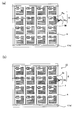
- FIGS. 1A to 1C are process diagrams showing an example of a method for producing a functional element of the present invention.
- FIGS. 1A to 1B correspond to cross-sectional views taken along the line XX in the schematic plan view of FIG. 1C, respectively.
- a functional layer forming coating solution 20 is applied in a pattern on the substrate 1, as shown in FIG. 1 (b).
- the functional layer 2 is formed.
- the functional layer 2 has a linear thin wire portion 2a and a wide area region 2b which is a region wider than the width of the thin wire portion 2a.
- the wide area region 2b is constituted by a plurality of wide area region constituting thin wires 2c having a width equal to the width of the thin wire portion 2a.
- the plurality of large area region constituting thin wires 2c are connected to each other and the thin wire portion 2a is connected. It is also characterized by the fact that they are also connected. Since the functional layer 2 has the above shape, as shown in FIGS.
- the application region G 2b corresponding to the wide area region 2b is changed to the application region G 2c corresponding to the wide area region constituting thin line 2c.
- Can be divided into it is possible to reduce the difference in the coating amount per unit area of the functional layer forming coating liquid 20 in the application region G 2b corresponding to the application region G 2a and wide area region 2b corresponding to the fine line portion 2a. Therefore, the film thickness unevenness of the functional layer 2 can be suppressed.
- a second functional layer 3 may be further formed in the present invention.
- the application region 3G corresponding to the second functional layer 3 is appropriately selected according to the thickness of the second functional layer 3 and the like.
- the functional element 10 can be manufactured by the above process.
- FIGS. 1B and 1C show an example in which the functional layer 2 is a conductive layer having conductivity and the functional element 10 is a TFT substrate.
- the functional layer 2 is a drain electrode
- the thin line portion 2a in the functional layer 2 is a linear conductive portion
- the large area region 2b in the functional layer 2 is a storage capacitor portion.
- An example is shown.
- the wide area region 2 b in the functional layer 2 is constituted by a wide area region constituting thin line 2 c in the plurality of functional layers 2.
- the second functional layer 3 is a source electrode is shown.
- FIGS. 3 (a) to 3 (b) are a schematic plan view and a schematic cross-sectional view showing another example of the method for producing a functional element of the present invention.
- FIGS. 3A to 3B are cross-sectional views taken along line XX of FIGS. 2A to 2B, respectively.
- a hydrophilic / hydrophobic pattern substrate 1a having a hydrophobic region A and a hydrophilic region B formed on its surface is prepared.
- the hydrophilic region B in the present invention includes a linear thin line portion B 2a and a wide area region B 2b that is wider than the width of the thin line portion B 2a .
- the wide area region B 2b is a thin line portion B.
- a plurality of wide area region constituting thin lines B 2c having a width equal to the width of 2a , and the plurality of large area region constituting thin lines B 2c are connected to each other and also connected to the thin line portion B 2a.
- the hydrophilic region B having at least the fine line portion B 2a and the large area region B 2b described above is formed.
- it may further have a second hydrophilic region 3B.
- the functional layer 2 and the second layer are formed by applying a functional layer forming coating solution onto the hydrophilic region B of the hydrophilic / hydrophobic pattern substrate 1a.
- the functional layer 3 is formed.
- the functional element 10 can be manufactured by the above process. 2B and 3B show an example in which the functional layer 2 is a conductive layer having conductivity and the functional element 10 is a TFT substrate. Further, the details of the functional layer 2 in FIGS. 2B and 3B can be the same as the contents described in FIGS. 1B and 1C, and thus the description thereof is omitted here. To do.
- the wide area region is constituted by a plurality of wide area region constituting thin wires having a width equal to the width of the thin wire portion, and the plurality of wide area region constituting thin wires are connected to each other and the thin wire
- a functional layer having a uniform thickness can be formed on the substrate. Therefore, the functional layer can be formed while suppressing the uneven thickness of the functional layer.
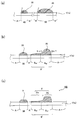
- the coating amount of the functional layer forming coating liquid per unit area applied to the coating area is: The larger the width of the coating area, the larger the thickness, and the thicker the functional layer obtained, the thicker the width of the coating area. More specifically, as shown in FIG. 11, since the contact angle ⁇ between the substrate 1 and the functional layer forming coating solution 20 is constant, the width is small when the widths of the coating regions 4G and 5G are different. The application amount of the functional layer forming coating solution 20 per unit area applied to the application region 5G having a width wider than that of the application region 4G increases.
- FIG. 11 is explanatory drawing explaining the relationship between the contact angle and coating amount of a coating liquid for a board
- the large area region 2′b is usually in a planar shape. It is formed.
- a functional layer having the above-described thin wire portion and a wide area region is formed using a functional layer forming coating solution, a difference in the thickness of the functional layer occurs due to the above-described width difference.
- the functional layer-forming coating liquid applied on the substrate usually has a property of gathering in a larger application amount due to surface tension. Therefore, as shown in FIG.
- FIG. 12 is a schematic plan view showing an example of a conventional functional element
- FIG. 13 is an explanatory diagram for explaining a functional layer forming coating solution in a conventional functional layer forming process
- FIG. 12 is a sectional view taken along line XX.
- the difference in thickness between the thin line portion and the large area in the functional layer becomes extremely large, for example, a portion where the thin line portion in the functional layer is too thin or not formed may occur. In this case, it may be difficult to exert the function of the functional layer in the thin line portion. Specifically, when the functional layer exhibits electrical conductivity, sufficient electrical conductivity cannot be exhibited in the thin line portion, which may cause electrical defects such as disconnection and short circuit.
- a coating method is used. When it is used, there is a problem that it may be difficult to form a coating film well, and when a printing method is used, for example, it may be difficult to print an accurate pattern.
- the present inventors as a functional layer design, when the functional layer has a linear thin line portion and a wide area region that is wider than the width of the thin line portion, the wide area region in the functional layer Is divided into a plurality of wide-area region-structured thin lines having a width equivalent to the width of the fine line portion of the functional layer, thereby making it possible to form the functional layer while suitably suppressing the uneven thickness of the functional layer.
- the headline and the present invention have been completed.
- the wide area region in the functional layer is constituted by a plurality of wide area region constituting thin lines having a width equivalent to the width of the thin line portion in the functional layer, and the plurality of wide area region constituting thin wires are respectively Are connected to each other and are also coupled to the thin line portion, so that the wide area region can be configured by a set of the plurality of wide area region constituting thin lines having a small width difference from the thin line portion.
- the difference in the application amount of the functional layer forming coating liquid per unit area applied to the application region corresponding to the part and the application region corresponding to the wide area region can be reduced, and the thin line part and the wide area in the functional layer can be reduced.
- the thickness of the region can be made uniform.
- the functional layer can be formed while suppressing the uneven thickness of the functional layer.
- the thickness of the fine line portion and the large area of the functional layer can be formed uniformly, for example, defects of the fine line portion in the functional layer can be prevented.
- a coating method when a coating method is used, a coating film can be formed satisfactorily, and when a printing method is used, for example, an accurate pattern can be printed well. can do.
- the functional layer formation process in this invention is a process of apply
- Substrate The substrate in the present invention is not particularly limited as long as the functional layer can be formed by applying a functional layer forming coating solution. Moreover, as a board
- Examples of the surface treatment include a hydrophilic / hydrophobic pattern treatment for forming a hydrophobic region and a hydrophilic region on the substrate surface, a surface unevenness treatment for forming surface unevenness on the substrate surface, and a self-assembled monomolecular film on the substrate surface.
- Chemical modification treatment for chemically modifying
- the substrate is preferably a hydrophilic / hydrophobic pattern substrate that has been subjected to hydrophilic / hydrophobic pattern processing.
- the functional layer can be formed with high definition by utilizing the difference in wettability between the hydrophilic region and the hydrophobic region.
- region can be formed by a simple method by apply
- hydrophobic / hydrophobic pattern substrate The hydrophilic / hydrophobic pattern substrate used in this step has a hydrophobic region and a hydrophilic region formed on the surface thereof.
- the functional layer forming coating liquid containing the functional layer material is applied only to the hydrophilic region by utilizing the wettability difference between the hydrophilic region and the hydrophobic region formed on the surface.
- patterning is performed. More specifically, patterning is performed by providing a difference in the contact angle of the functional layer forming coating solution between the hydrophilic region and the hydrophobic region.
- the contact angle with the functional layer forming coating solution is adjusted to be a constant value. Therefore, since the contact angles of the hydrophilic region and the functional layer forming coating liquid are constant, when the widths of the hydrophilic regions 4B and 5B are different as shown in FIG.
- the application amount of the functional layer forming coating solution 20 per unit area applied to the region 5B increases. Further, as shown in FIG. 15B, in the hydrophilic region B ′ having the thin line portion B 2′a and the wide area region B 2′b , the fine line is formed by the surface tension T of the functional layer forming coating solution 20. The functional layer forming coating solution 20 agglomerates from the part B 2′a toward the large area B 2′b . Therefore, even when the conventional functional layer 2 ′ is formed using the hydrophilic / hydrophobic pattern substrate 1a as shown in FIG. 15C, it is difficult to form the functional layer 2 ′ while suppressing the film thickness unevenness. is there.
- FIGS. 15A to 15C are explanatory views for explaining the hydrophilic / hydrophobic pattern substrate. Further, A in FIGS. 15B and 15C indicates a hydrophobic region.
- the hydrophobic region in the hydrophilic / hydrophobic pattern substrate used in this step is a region showing hydrophobicity
- the hydrophilic region is a region showing hydrophilicity.
- “hydrophobic” in the present invention refers to a case where the contact angle with water at 25 ° C. is 50 ° or more.
- “hydrophilic” in the present invention means that the contact angle of water at 25 ° C. is less than 50 °.
- the contact angle in the present invention is measured by, for example, dropping 1 microliter of liquid on a substrate, observing the shape of the dropped droplet from the side, and measuring the angle formed by the droplet and the substrate. can do.
- the contact angle in the present invention can be measured using, for example, a contact angle measuring device manufactured by Imoto Seisakusho. Further, the contact angle in the present invention can be measured using, for example, a contact angle meter DM-901 manufactured by Kyowa Interface Science.
- the hydrophobic region in the present invention is more preferable as the hydrophobicity is higher. More specifically, the hydrophobic region in the present invention is not particularly limited as long as the contact angle with water at 25 ° C. is 50 ° or more, but is preferably 70 ° or more, more preferably 80 ° or more. Further preferred.
- the hydrophilic region in the present invention is more preferable as the hydrophilicity is higher. More specifically, the hydrophilic region in the present invention is not particularly limited as long as the contact angle with water at 25 ° C. is less than 50 °, but is preferably 30 ° or less, more preferably 20 ° or less. Is more preferable.
- the difference between the contact angles in the hydrophilic region and the hydrophobic region in the present invention is preferably 10 ° or more, more preferably 40 ° or more, and further preferably 70 ° or more. preferable.
- the hydrophobicity of the hydrophobic region and the hydrophilicity of the hydrophilic region are higher, the difference in contact angle between the hydrophilic region and the hydrophobic region can be increased. Coloring can be performed with high definition. Therefore, a higher-definition functional layer can be formed.
- region in this invention is an area
- region in this invention is an area
- the wide area region is constituted by a plurality of wide area region constituting thin lines having a width equal to the width of the thin line portion.
- the large area of the hydrophilic region is provided so that the large area of the functional layer formed on the surface can exert its function.
- region of a functional layer can exhibit the function by forming in an area wider than a thin wire
- the function of the wide area region of the functional layer for example, the storage capacity of the drain electrode in the TFT substrate can be cited.
- the wide area region is a region wider than the width of the thin line portion. “The wide area region is a region wider than the width of the thin line portion” means that the width of the outer shape in a plan view of the wide area region in the direction perpendicular to the width direction of the thin line portion and the width in the width direction and horizontal direction of the thin line portion. It means that both of the widths of the outer shape in plan view of the area region are larger than the width of the thin line portion.
- the “width of the thin line portion” refers to the line width of the thin line portion formed in a linear shape, for example, the distance indicated by x1 in FIG.
- the “outer shape of the wide area region in plan view” refers to a shape formed by the outer periphery of the large area region. Further, when the plan view shape of the large area region has a gap portion F1 having an opening on the outer periphery of the large area region as shown in FIGS. 4A and 5A described later, the space between the openings is continuous. The shape formed by the outer periphery when it is assumed.
- the “outer shape in plan view of the wide area region” refers to, for example, a shape indicated by a broken line in FIGS. 4A and 5A, and more specifically, FIGS. 4B and 5B. The shape C surrounded by a solid line in FIG.
- the “notch portion of the planar view outer shape of the large area region” means a portion in which a part of the above figure is removed from the graphic including the planar view outer shape of the large area region, and more specifically, As shown in FIG. 4B, in the figure D including the outline shape C in plan view (the shape D surrounded by the alternate long and short dash line), a part E from which a part of the figure D is removed (the part E indicated by diagonal lines) ).
- the width of the outer shape in plan view of the wide area region in the direction perpendicular to the width direction of the thin line portion refers to a distance indicated by x2 in FIGS. 4A and 5A, for example.
- the width of the outer shape in plan view of the wide area region in the width direction and the horizontal direction of the thin line portion refers to, for example, a distance indicated by x3 in FIGS. 4 (a) and 5 (a).
- the “planar shape of the large area region” is a hydrophobicity disposed between the wide area region forming thin line formed in the large area region and the adjacent large area region disposed in the large area region.
- the “planar shape of the wide area region” means, for example, the wide area region constituting thin line B 2c in FIGS. 4 (a), 5 (a), 6 (a) to 6 (b), 7 and 8.
- interval part it may have an opening in the outer periphery of a large area area
- the “gap portion having an opening on the outer periphery of the large area region” refers to a gap portion having a portion continuous with the hydrophobic region located outside the large area region, and more specifically, FIG. ), A portion indicated by F1 in FIGS. 5 (a), 6 (a) to 6 (b) and FIG.
- the “gap portion having no opening on the outer periphery of the large area region” more specifically refers to a portion indicated by F2 in FIGS. 4 (a)-(b), FIGS. 5 (a)-(b), FIGS. 6 (a)-(b), FIG. 7 and FIG. 8 are used to explain examples of hydrophilic regions in the present invention.
- the wide area region is a region wider than the width of the thin line portion
- the wide area region means more specifically x2 and x3 in the hydrophilic region B shown in FIG. 4A, FIG. Both of the distances indicated by are larger than the distance indicated by x1.
- the ratio of the width of the planar view outer shape of the wide area region when the width of the thin line portion is 1 it can be appropriately selected according to the type of the functional element, and is not particularly limited. Especially, it is preferable that it is 5 or more, especially 10 or more.
- the ratio of the width of the planar area of the wide area region to the width of the thin line portion is less than the above-described range, it may be difficult to configure the wide area region with a plurality of wide area region configuration thin lines, This is because it may be difficult for the large area region to have a predetermined function when the large area region is constituted by a plurality of wide area region constituting thin lines.
- the specific width of the outer shape in plan view of the wide area region can be appropriately selected according to the type of the functional element of the present invention, and is not particularly limited.
- the width is in the range of 40 ⁇ m to 5000 ⁇ m. It is preferably in the range of 80 ⁇ m to 1000 ⁇ m, particularly in the range of 100 ⁇ m to 500 ⁇ m. This is because functional layers of various functional elements can be formed.
- the external shape of the wide area region in plan view can be appropriately selected according to the type of the functional element of the present invention, and is not particularly limited, but is preferably a square shape such as a square or a rectangle. This is because, when the outer shape of the large area area in plan view is a quadrangular shape, it can be satisfactorily constituted by a plurality of thin line portions. In this case, the outer shape of the wide area region in plan view may have a notch.
- the shape of the wide area region in plan view is appropriately determined according to the arrangement of a plurality of wide area region constituting thin lines described later.
- the shape of the wide area region in plan view may be any shape having a wide area region forming thin line and a gap, as shown in FIGS. 4 (a), 5 (a), and 6 (a) to 6 (b).
- the shape may have only the gap portion F1 having an opening on the outer periphery of the large area region B 2b , and only the gap portion F2 having no opening on the outer periphery of the large area region B 2b as shown in FIG.
- the shape may be sufficient, and as shown in FIG. 7, the shape which has both F1 and F2 may be sufficient.
- FIG. 7 the shape which has both F1 and F2 may be sufficient.
- a gap portion having an opening at least on the outer periphery of the wide area region B 2b Preferably, it has a shape having F1, and as shown in FIGS. 4 (a), 5 (a), and 6 (a) to 6 (b), only the gap portion F1 having an opening on the outer periphery of the large area B2b. It is preferable that it is a shape which has.
- the functional layer forming coating applied on the adjacent wide area region forming thin line
- the shape of the wide area region in plan view includes a shape including a stripe and a mesh shape.
- the wide area region is constituted by a plurality of wide area region constituting thin lines having a width equal to the width of the thin line portion.
- the plurality of wide area region constituting thin wires are connected to each other and also joined to the thin wire portion.
- the "plurality of large area region constituting thin lines are respectively connected", for example, wide area region thin lines adjacent in the plurality of large area regions constituting fine line B 2c1 ⁇ B 2c8 as shown in FIG. 4 (a) B 2c1 and B 2c2, coupled by B 2c2 and B 2c3, B 2c3 and B 2c4, B 2c4 and B 2c5, B 2c5 and B 2c6, B 2c6 and B 2C7, and B 2C7 and B 2C8 is large area extent configuration thin line B 2C9 Including cases where
- the wide area region constituting thin wire has the same width as the width of the thin line portion
- the difference between the width of the wide area region constituting thin line and the width of the thin line portion is applied to the functional layer forming coating. It means that the coating amount of the liquid is equal to the coating amount of the functional layer forming coating liquid applied to the wide area region constituting thin line.
- the amount of the functional layer forming coating liquid applied to the thin line portion is equal to the amount of the functional layer forming coating liquid applied to the wide area region constituting thin line”
- the difference in coating amount between the fine line portion and the large area region is due to the difference in thickness between the fine line portion and the large area region in the functional layer, which is caused by the movement of the coating liquid for forming the functional layer between the hydrophilic regions due to surface tension. The difference between the two functions is not inhibited.
- the ratio of the width of the wide area region constituting thin line to the width of the thin line portion is too large, even if the wide area region is constituted by a plurality of wide area region constituting thin lines, the thin line portion and the wide area in the functional layer This is because it may be difficult to sufficiently reduce the difference in thickness of the regions.
- the specific width of the wide area region constituting thin line can be appropriately selected according to the type of the functional layer forming coating solution, and is not particularly limited. For example, it is in the range of 2 ⁇ m to 200 ⁇ m, and in particular, 5 ⁇ m. It is preferable to be in the range of ⁇ 100 ⁇ m, particularly in the range of 10 ⁇ m to 40 ⁇ m. This is because the fine wire having a large area of the functional layer can be formed satisfactorily on the base material.
- the “width of the wide area region constituting thin line” means a line width of the wide area region constituting thin line formed in a linear shape, for example, a distance indicated by x4 in FIG.
- the length of the specific wide area region constituting thin line is appropriately selected according to the external shape of the wide area region in plan view.
- the arrangement of the plurality of wide area region constituting thin lines is appropriately selected according to the outer shape of the wide area region in plan view, and is not particularly limited, but the outer periphery of the wide area region is not closed by the wide area region constituting thin lines, In other words, the arrangement is preferably such that a gap having an opening is sandwiched around the outer periphery of the large area region.
- the arrangement of the plurality of wide area region constituting thin lines is such that the gap having openings at the outer periphery of the large area region is sandwiched.
- the functional layer forming coating liquid applied on the wire can be prevented from contacting at the gap, and a plurality of wide area region constituting fine lines in the functional layer can be arranged more finely so that the wide area region in the functional layer is formed. It is because it can form.
- the gap portion is formed by arranging the plurality of wide area region constituting thin lines in the above-described arrangement. The contact of the functional layer forming coating solution in can be suitably suppressed.
- the arrangement including the gap portion having the opening on the outer periphery of the wide area region is preferably an arrangement including a stripe arrangement, for example.
- a plurality of wide area region constituting thin lines are arranged in the width direction and the horizontal direction of the thin line portion B 2a.
- An arrangement in which B 2c is arranged in a stripe shape and the wide area region constituting fine lines B 2c adjacent to each other at one end of the stripe arrangement are combined, or the width direction of the fine line portion B 2a as shown in FIG.
- the width direction and the stripe arrangement in which a plurality of large area regions constituting thin line B 2c are arranged in the horizontal direction, the width direction and the vertical direction of the thin line portion B 2a of the fine line portion B 2a Alternatively, an array may be combined with a stripe array in which a plurality of wide area region forming thin lines B 2c are arrayed.
- the pitch width of the stripe arrangement can be appropriately selected according to the type of coating liquid for forming the functional layer, and is not particularly limited. It is preferably in the range of ⁇ 400 ⁇ m, in particular in the range of 10 ⁇ m to 200 ⁇ m, particularly in the range of 20 ⁇ m to 80 ⁇ m. This is because, when the pitch width of the stripe arrangement is too narrow, adjacent wide area region constituting fine lines may come into contact with each other in the hydrophobic region. Moreover, it is because it may become difficult to provide a predetermined function to a wide area area
- the pitch width of the stripe arrangement refers to the distance between the centers of adjacent wide area region constituting thin wires, for example, the distance indicated by x5 in FIG.
- the interval between the stripe arrangements can be appropriately selected according to the type of the functional layer forming coating solution, and is not particularly limited. It is preferably in the range of 200 ⁇ m, especially in the range of 5 ⁇ m to 100 ⁇ m, particularly in the range of 10 ⁇ m to 40 ⁇ m. This is because if the stripe arrangement interval is too narrow, adjacent wide-area region constituting fine lines may come into contact with each other in the hydrophobic region. If the stripe arrangement interval is too wide, a predetermined large area region is set. This is because it may be difficult to provide this function.
- the interval between the stripe arrangements means a distance between adjacent wide area region forming thin lines, for example, a distance indicated by x6 in FIG.
- an array of a plurality of wide area region constituting thin lines an array in which the outer periphery of the wide area region is closed by the wide area region constituting thin lines, that is, an array having a gap portion having no opening on the outer periphery of the large area region.
- An arrangement in which the gaps F2 having no gaps are sandwiched can be given.
- the width, pitch width, and interval between the wide area region constituting thin lines can be the same as those of the array including the stripe arrangement described above, and thus the description thereof is omitted here. .
- the area in which the wide area region constituting thin line is formed in the wide area region (hereinafter, may be referred to as the area of the wide area region constituting thin line) is as long as the function of the wide area region can be secured. It does not specifically limit and can be suitably selected according to the kind of functional element.
- the ratio of the area of the wide area region constituting thin wire to the area of the entire large area region is in the range of 0.10 to 0.95, in particular in the range of 0.30 to 0.90, particularly 0. It is preferably in the range of 40 to 0.70.
- the ratio of the area of the wide area region constituting thin wire is too large, it is not possible to sufficiently secure a gap portion disposed between each wide area region constituting thin wire, and the functional layer forming coating solution is applied. This is because there is a possibility that the functional layer forming coating liquid applied on the adjacent wide area region constituting thin wires may come into contact with the gap portion.
- the area ratio of the above-mentioned wide area region constituting thin wire is small, other layers can be formed on the wide area region of the functional layer to ensure the function of the large area region, From the viewpoint of safety, it is preferable that the area ratio of the wide area region constituting thin wires is adjusted so as to be formed as a single layer.
- Fine wire portion The fine wire portion in the present invention is formed in a linear shape and is coupled to the above-described wide area region constituting fine wire.
- the specific width of the thin wire portion can be made equal to the width of the above-described wide area region constituting thin wire, description thereof is omitted here.
- the length of the thin wire portion, the shape in plan view, and the like are appropriately selected according to the type of functional element.
- the “length of the thin line portion” refers to a distance indicated by x7 in FIG.
- (B) Second hydrophilic region The hydrophilic / hydrophobic pattern substrate used in this step only needs to have a hydrophilic region having a fine line portion and a wide area, and for example, FIG. 2 (a) and FIG. As shown to 3 (a), the 2nd hydrophilic region 3B which has only a thin wire
- variety of a 2nd hydrophilic region since it can be made equal to the width
- hydrophobic region in the present invention is usually formed in a region other than the hydrophilic region and the second hydrophilic region formed as necessary on the surface of the hydrophilic / hydrophobic pattern substrate.
- Such a hydrophilic / hydrophobic pattern substrate has a structure in which a hydrophilic region is formed in a desired pattern on the surface of the hydrophobic substrate including a hydrophobic material (the hydrophilic / hydrophobic pattern substrate of the first aspect) and A hydrophilic substrate having a hydrophilic surface and a hydrophobic layer formed on the hydrophilic substrate and having hydrophobic properties, the hydrophobic layer being removed in a pattern, and the surface of the hydrophilic substrate being patterned And the one having a configuration exposed in a shape (the hydrophilic / hydrophobic pattern substrate of the second embodiment).
- the hydrophilic / hydrophobic pattern substrate of each of these embodiments will be described.
- Hydrophilic / hydrophobic pattern substrate of the first aspect has a structure in which a hydrophilic region is formed in a desired pattern on the surface of the hydrophobic substrate whose surface contains a hydrophobic material. It is.
- the hydrophobic substrate in this embodiment may be any substrate as long as at least the surface thereof contains a hydrophobic material capable of imparting hydrophilicity by performing a predetermined hydrophilic treatment.
- the hydrophobic substrate itself is hydrophobic. It may be made of a material, or may be one in which a layer containing a hydrophobic material is formed on a hydrophilic substrate such as glass, SiO 2 , SiN, or SiON.
- the hydrophobic material in this embodiment may be an organic material or an inorganic material.
- examples of the hydrophobic material used for the hydrophobic substrate in this embodiment include polystyrene, polyimide, polyester, polyethylene, polyphenylene sulfide, polyparaxylene, polyethylene terephthalate, polyethylene naphthalate, and polydimethylsiloxane.
- any of these hydrophobic materials can be suitably used.
- only a single type of hydrophobic material may be used, or a plurality of types of hydrophobic materials may be used.
- the thickness of the hydrophobic substrate in this embodiment is within a range in which desired self-supporting property, flexibility, and the like can be imparted to the hydrophobic substrate according to the use of the functional element of the present invention. It is not particularly limited. In particular, the thickness of the hydrophobic substrate in this embodiment is preferably in the range of 1 ⁇ m to 5 mm, more preferably in the range of 10 ⁇ m to 1.5 mm, and in the range of 25 ⁇ m to 1.0 mm. Is more preferable.
- Examples of the method for forming the hydrophilic / hydrophobic pattern substrate of this embodiment include a method of forming a patterned hydrophilic region on the hydrophobic substrate of this embodiment. More specifically, the surface of the hydrophobic substrate is patterned.
- the method of hydrophilizing can be mentioned.
- the method for hydrophilizing the surface of the hydrophobic substrate is not particularly limited as long as it is a processing method capable of forming a hydrophilic region having a desired hydrophilicity depending on the type of hydrophobic material constituting the hydrophobic substrate. Is not to be done.
- Examples of such a method include a method of irradiating the surface of the hydrophobic substrate with ultraviolet rays, an electron beam or a laser through a photomask, or an active radiation such as ultraviolet rays directly in a pattern on the surface of the hydrophobic substrate.
- the method etc. which irradiate can be mentioned.
- the hydrophobic material used for the hydrophobic substrate has the property of being partially decomposed by irradiation with ultraviolet rays or the like to generate OH groups
- the surface of the hydrophobic substrate is irradiated with ultraviolet rays in a pattern. By doing so, it is possible to form a hydrophilic region that is made hydrophilic by generating OH groups on the surface.
- hydrophilic / hydrophobic pattern substrate of the second aspect includes a hydrophilic substrate having a hydrophilic surface and a hydrophobic layer formed on the hydrophilic substrate and exhibiting hydrophobicity. The hydrophobic layer is removed in a pattern, and the surface of the hydrophilic substrate is exposed in a pattern.
- hydrophilic substrate The material constituting the hydrophilic substrate used for the hydrophilic / hydrophobic pattern substrate of the second aspect (hereinafter referred to as “hydrophilic material”) is not particularly limited as long as it can produce a hydrophilic substrate having desired hydrophilicity. It is not a thing. Therefore, the hydrophilic material used in this embodiment may be an inorganic material or an organic material. Examples of such a hydrophilic material include glass, SiO 2 , SiN, and SiON.
- a hydrophobic substrate including a hydrophobic material such as polyimide, polyester, polyethylene, polyphenylene sulfide, or polyparaxylene is subjected to a hydrophilic treatment using ultraviolet light, electron beam, laser, or the like.
- a hydrophilic treatment using ultraviolet light, electron beam, laser, or the like can be mentioned.
- any hydrophilic substrate made of any of these hydrophilic materials can be preferably used.
- the hydrophobic substrate is hydrophilized using ultraviolet light, electron beam, laser, or the like. It is preferable to use one that has been treated.
- the thickness of the hydrophilic substrate used for the hydrophilic / hydrophobic pattern substrate of the second aspect desired self-supporting property, flexibility, etc. are imparted to the hydrophilic substrate according to the use of the functional element of the present invention. If it is in the range which can do, it will not specifically limit.
- the thickness of the hydrophilic substrate used in this embodiment is preferably in the range of 1 ⁇ m to 5 mm, more preferably in the range of 10 ⁇ m to 1.5 mm, and in the range of 25 ⁇ m to 1.0 mm. More preferably it is.
- the hydrophobic layer used in the hydrophilic / hydrophobic pattern substrate of the second embodiment is not particularly limited as long as it has the above hydrophobic property, but among them, one that can be removed in a pattern is preferable.
- the hydrophobic layer used in this embodiment is preferably a self-assembled monolayer made of a self-assembled monolayer material. This is because when the hydrophobic layer is a self-assembled monomolecular film, it becomes easy to remove the hydrophobic layer in a high-definition pattern.
- the self-assembled monolayer material is not particularly limited as long as it can form a hydrophobic layer made of a self-assembled monolayer having a desired hydrophobicity.
- self-assembled monolayer materials include HMDS (hexamethyldisilazane), OTS (octyltrichlorosilane), ODTS (octadecyltrichlorosilane), FAS (fluorinated alkylsilane), alkyltrimethoxysilane. And alkyltriethoxysilane.
- any of these self-assembled monolayer materials can be suitably used.
- HMDS hexamethyldisilazane
- OTS octyltrichlorosilane
- ODTS octadecyltrichlorosilane
- the thickness of the hydrophobic layer is not particularly limited and can be appropriately determined according to the material used for forming the hydrophobic layer.
- the hydrophilic substrate in the second embodiment can produce a hydrophilic / hydrophobic patterned substrate by removing the hydrophobic layer in a pattern, the thickness of the hydrophobic layer is removed in a pattern. It is preferable that it is easy to do.
- the thickness of the hydrophobic layer used in this embodiment is preferably in the range of 0.1 nm to 1 ⁇ m, more preferably in the range of 0.1 nm to 100 nm, and 0.1 nm More preferably, it is in the range of ⁇ 10 nm.
- Method for forming hydrophilic / hydrophobic pattern substrate As a method for forming the hydrophilic / hydrophobic pattern substrate of this embodiment, for example, when the above-described hydrophilic substrate is used, the hydrophobic layer is removed in a pattern and the surface of the hydrophilic substrate is exposed in a pattern. be able to.
- the hydrophobic layer is formed according to the configuration of the hydrophobic layer. There is no particular limitation as long as it can be removed. However, in this method, since the hydrophilic region is formed by exposing the surface of the hydrophilic substrate, the method of removing the hydrophobic layer is a method that can remove the hydrophobic layer almost completely. It is preferable.
- the surface of the hydrophobic layer is irradiated with ultraviolet rays through a photomask to decompose and remove the hydrophobic layer, or the surface of the hydrophobic layer is exposed to ultraviolet rays, electron beams, plasma, etc.
- Examples of the method of irradiating the active radiation in a pattern include a method of decomposing and removing the hydrophobic layer.
- both the hydrophilic / hydrophobic pattern substrate of the first aspect and the hydrophilic / hydrophobic pattern substrate of the second aspect described above can be used, but it is more preferable to use the hydrophilic / hydrophobic pattern substrate of the second aspect.
- a hydrophobic layer made of a self-assembled monolayer is formed in the region. Since the hydrophobic layer made of a self-assembled monolayer can be easily removed in a pattern by ultraviolet irradiation or the like, a hydrophilic / hydrophobic pattern substrate having a high-definition hydrophilic region and a hydrophobic region pattern can be obtained. Because.
- the substrate used in this step is not limited to the hydrophilic / hydrophobic pattern substrate, and can be appropriately selected according to the type of functional element.
- a general glass substrate or resin substrate can be used.
- substrate what has a sheet form, a film form, and a plate-shaped form can be used.
- the functional layer forming coating liquid used in this step usually contains a functional layer material and a solvent.
- the material for the functional layer can be appropriately selected according to the type of the functional element, and is not particularly limited.
- the material for the functional layer is preferably a conductive material.
- a conductive layer having conductivity can be formed as the functional layer, and unevenness of the film thickness of the conductive layer can be suppressed, so that occurrence of electrical defects such as disconnection and short circuit in the thin wire portion can be suppressed. .
- region in a conductive layer can be made uniform, it can be set as the conductive layer which shows favorable electroconductivity.
- the conductive material include metal particles or metal oxide particles such as Au, Cu, Ag, ITO, and Pt, carbon materials such as graphene and carbon nanotubes, and conductive polymer materials such as PEDOT / PSS. .
- Examples of the solvent in the functional layer-forming coating solution include water, acetone, methanol, ethanol, isopropyl alcohol, propylene glycol 1-monomethyl ether 2-acetate, toluene, xylene, mesitylene, tetralin, decahydronaphthalene, chlorobenzene, dibenzene, and the like. And chlorobenzene.
- a coating liquid for forming a functional layer is applied onto a substrate to form a thin line portion and a wide area region having a plurality of wide area region constituting thin lines.
- the functional layer can be formed.
- a method of applying a functional layer forming coating solution in a pattern can be mentioned, and specific examples include an ink jet method and a nozzle jet method.
- a functional layer forming coating solution is applied onto the hydrophilic region of the hydrophilic / hydrophobic pattern substrate.
- the method for applying the functional layer forming coating solution on the hydrophilic / hydrophobic pattern substrate is particularly limited as long as it is a method capable of forming a coating film of the functional layer forming coating solution on the hydrophilic region of the hydrophilic / hydrophobic pattern substrate. Is not to be done.
- a method of applying the functional layer forming coating solution a method of applying to the entire surface of the hydrophilic / hydrophobic pattern substrate is preferably used.
- the functional layer can be formed by a simple method because the coating liquid for forming the functional layer can be selectively applied to the hydrophilic region by utilizing the difference in hydrophilicity and hydrophobicity on the surface of the hydrophilic / hydrophobic pattern substrate. Because you can.
- coating methods include generally known methods such as spin coating, capillary coating, die coating, roll coating, bar coating, dip coating, spray coating, blade coating, and gravure offset printing.
- the coating method can be used.
- a method of applying the functional layer forming coating solution onto the hydrophilic / hydrophobic pattern substrate a method of applying the above-described functional layer forming coating solution in a pattern can also be used.
- the functional layer formed in this step is formed on the substrate described above.
- the functional layer has a thin line portion and a wide area region composed of a plurality of wide area region constituting thin lines.
- the thin line portion, the wide area region, and the wide area region constituting thin line can be the same as those described in the above-mentioned section of “1.
- the thickness of the functional layer is appropriately selected according to the type of the functional element of the present invention, and is not particularly limited. For example, it can be set to about 30 nm to 500 nm.
- the functional layer in the present invention has the above-described wide area region, the difference between the thickness of the thin line portion and the thickness of the wide area region in the functional layer is reduced, and the thickness of the functional layer is made uniform. be able to. More specifically, the absolute value of the difference between the thickness of the fine line portion and the thickness of the large area in the functional layer is 200 nm or less, preferably 100 nm or less, and particularly preferably 30 nm or less. preferable.
- the absolute value of the difference between the thickness of the fine line portion in the functional layer and the thickness of the wide area region is large, for example, it may be difficult to exhibit predetermined conductivity in the fine line portion in the functional layer, or for example, the functional layer This is because it may be difficult to satisfactorily form another layer on the large area region.
- the thickness of the thin line portion in the functional layer and the thickness of the wide area region can be measured by, for example, Surfcoder SE4000 manufactured by Kosaka Laboratory Ltd.
- the thickness of the wide area region in the functional layer is the average value obtained by measuring the thickness of each of the plurality of wide area region constituting thin wires constituting the wide area region and averaging the obtained measurement values. To do.
- the functional layer in the present invention is not particularly limited as long as it has the fine line portion and the large area described above.
- the drain electrode in the substrate for TFT illustrated in FIG. When the functional layer is the drain electrode, for example, the linear conductive portion corresponds to a thin line portion, and the storage capacitor portion corresponds to a wide area region.
- examples of the functional layer include a wiring layer and a sensor unit in the touch panel sensor illustrated in FIGS. 9 to 10.
- FIG. 9 is a schematic plan view showing another example of the functional element manufactured according to the present invention
- FIG. 10 is a sectional view taken along line XX of FIG. 9 and 10 show an example in which the functional element 10 is a projected capacitive touch panel sensor.
- the touch panel sensor shown in FIG. 9 and FIG. 10 includes an insulating base material 11, a sensor portion 23 formed on the insulating base material 11, and a wiring layer 24.
- the sensor unit 23 is formed in the active area of the touch panel sensor, and usually the sensor electrode having the first electrode 21b and the second electrode 22b and the first conductive unit 21a and the second electrode 22b that connect the first electrode 21b to each other. And a conductive portion having a second conductive portion 22a for connecting the two.
- the wiring layer 24 includes a lead-out wiring 24a formed outside the active area and connected to the sensor electrode, and an external connection terminal 24b connected to the lead-out wiring 24a. 9 and 10, the first electrode 21b, the first conductive portion 21a, the lead wire 24a connected to the first electrode 21b and the external connection terminal 24b on the two insulating base materials 11, respectively.
- the second electrode 22b, the second conductive portion 22a, the lead wire 24a connected to the second electrode 22b, and the external connection terminal 24b are formed, and the two insulating base materials 11 are bonded together with the insulating layer 4 interposed therebetween.
- An example is shown.
- the functional layer 2 in the present invention is the wiring layer 24 described above
- the insulating substrate 11 corresponds to the hydrophilic / hydrophobic pattern substrate 1a
- the lead-out wiring 24a corresponds to the thin wire portion 2a
- the external connection terminal 24b corresponds to the wide area region 2b. It corresponds to.
- the insulating base material 11 corresponds to the hydrophilic / hydrophobic pattern substrate 1a
- the first conductive portion 21a and the second conductive portion 22a correspond to the thin wire portion 2a
- the first electrode 21b and the second electrode 22b correspond to the wide area region 2b.
- the sensor electrode, conductive portion, lead-out wiring, external connection terminal, and other aspects of the touch panel sensor and other details of the touch panel sensor can be the same as those of a general touch panel sensor, for example, Japanese Patent Laid-Open No. 2013-210732 Since it can be the same as that described in JP 2013-210733 A, description thereof is omitted here.
- a wiring layer in a display panel can be cited.
- the wiring layer can be the same as that used for a general display panel, and usually has a lead-out wiring and an external connection terminal.
- the lead-out wiring corresponds to the thin line portion
- the external connection terminal corresponds to the wide area region.
- the functional layer forming step in the present invention may be performed as long as the functional layer can be formed on the substrate.
- the hydrophilic / hydrophobic pattern substrate has the second hydrophilic region
- the second function is formed on the second hydrophilic region. Layers can be formed simultaneously.
- Examples of the second functional layer formed on the second hydrophilic region include a source electrode on a TFT substrate and a pixel electrode on a display panel substrate.
- the method for producing a functional element of the present invention is not particularly limited as long as it has the functional layer forming step described above, and other steps can be appropriately selected and added as necessary. Examples of such a process include a process of forming a hydrophilic / hydrophobic pattern substrate and a process of forming with another layer on the functional layer.
- the functional element produced according to the present invention is not particularly limited as long as it has the above-described functional layer. Examples thereof include a TFT substrate, a touch panel sensor, and a display panel substrate.
- the touch panel sensor has two insulating bases as shown in FIGS. 9 and 10
- the touch panel member having the insulating base on which each conductive portion and sensor electrode are formed is also a functional element. be able to.
- the manufacturing method of the TFT substrate of the present invention is the above-described “A. Functional element manufacturing method”, in which the functional layer is a conductive layer having conductivity, and the conductive layer is a TFT.
- This is a manufacturing method characterized by being a part of the structure. That is, the TFT substrate manufacturing method of the present invention is a manufacturing method having a conductive layer forming step of forming a conductive layer having conductivity by applying a conductive layer forming coating solution containing a conductive material on the substrate.
- the conductive layer has a linear thin line portion and a wide area region that is wider than the width of the thin line portion, and the wide area region has a width equivalent to the width of the thin line portion.
- the manufacturing method is characterized in that the plurality of wide area region constituting thin lines are connected to each other and are also coupled to the thin line portion.
- FIGS. 1A to 1C, FIGS. 2A to 2B, and FIGS. 3A to 3B are schematic plan views showing an example and another example of a method for manufacturing a TFT substrate of the present invention.
- FIG. Details of FIGS. 1A to 1C, FIGS. 2A to 2B, and FIGS. 3A to 3B are described above in the section “A. Functional element manufacturing method”. Therefore, the description is omitted here.
- the wide area region is constituted by a plurality of wide area region constituting thin wires having a width equal to the width of the thin wire portion, and the plurality of wide area region constituting thin wires are connected to each other and the thin wire
- a conductive layer having a uniform thickness can be formed on the substrate. Therefore, the conductive layer can be formed while suppressing unevenness in the thickness of the conductive layer. That is, in the present invention, the conductive layer which is a part of the structure of the thin film transistor can be formed while suppressing unevenness in film thickness.
- the conductive material and solvent used in the conductive layer forming coating solution, the coating method, and the conductive layer the above-mentioned “A. Functional element manufacturing method” Since it can be the same as that described in the section, description thereof is omitted here.
- the functional element of the present invention has a substrate and a functional layer formed on the substrate, and the functional layer has a linear fine line portion and a width of the fine line portion.
- a wide area that is a wide area, and the wide area area is configured by a plurality of wide area area configuration thin lines having a width equal to the width of the thin line portion, and the plurality of wide area area configuration thin lines are These are connected to each other and are also connected to the thin line portion.
- FIG. 1 (b), (c), FIG. 2 (b) and FIG. 3 (b), and FIG. 9 and FIG. 10 are schematic plan views and sectional views showing an example of the functional element of the present invention and other examples. is there. Note that the details of these drawings can be the same as the contents described in the section “A. Functional element manufacturing method”, and thus the description thereof is omitted here.
- the functional layer having a uniform thickness can be formed by having the above-described wide area region, it is possible to obtain a functional element in which the thickness unevenness of the functional layer is suppressed.
- the fine line portion the wide area region and the wide area region constituting thin line in the functional layer, the thin line portion, the wide area region and the wide area region constitution in the hydrophilic region described in the above-mentioned section of “A. Since it can be the same as that of a thin wire
- the configuration of the functional element of the present invention can be the same as the content described in the above-mentioned section “A. Functional element manufacturing method”, and thus the description thereof is omitted here.
- the TFT substrate of the present invention is such that, in the above-mentioned “C. Functional element”, the functional layer is a conductive layer having conductivity, and the conductive layer is part of the structure of the TFT. It is characterized by. That is, the TFT substrate of the present invention includes a substrate and a conductive layer having conductivity formed on the substrate, and the conductive layer includes a linear thin wire portion and the thin wire portion. A wide area region that is wider than the width of the thin line portion, and the wide area region is configured by a plurality of wide area region configuration thin wires having a width equal to the width of the thin wire portion, and the plurality of wide area regions The constituent thin wires are connected to each other and are also connected to the thin wire portion.
- FIGS. 1B, 1C, 2B, and 3B are a schematic plan view and a cross-sectional view showing an example of a TFT substrate of the present invention. Note that the details of these drawings can be the same as the contents described in the section “A. Functional element manufacturing method”, and thus the description thereof is omitted here.
- the conductive layer having a uniform thickness can be formed by having the above-described wide area region, a thin film transistor substrate in which unevenness in the thickness of the conductive layer is suppressed can be obtained. That is, in the present invention, the conductive layer can have a nonuniform thickness, and can be suitably used as part of the structure of the thin film transistor.
- the configuration of the TFT substrate of the present invention can be the same as that described in the above-mentioned section “A. Method for manufacturing functional element”, and thus the description thereof is omitted here.
- the present invention is not limited to the above embodiment.
- the above-described embodiment is an exemplification, and the present invention has substantially the same configuration as the technical idea described in the claims of the present invention, and any device that exhibits the same function and effect is the present invention. It is included in the technical scope of the invention.
- Example 1 (Production of metal mask) A metal mask having an opening corresponding to the shape of the source / drain electrode illustrated in FIG. In the opening of the metal mask, the line width corresponding to B 2a of the drain electrode in FIG. 2A is 20 ⁇ m, and the line width corresponding to B 2c is 20 ⁇ m.
- the details of the shape of the opening corresponding to the drain electrode of the metal mask in plan view are the same as the shape of the drain electrode described later in plan view.
- Styrene polymer (Wako Pure Chemical Industries) was dissolved in propylene glycol 1-monomethyl ether 2-acetate (Kanto Kagaku Special Grade) at a concentration of 5 wt% to obtain a styrene polymer solution.
- the styrene polymer solution was applied onto a glass substrate with a spin coater (Mikasa MS-A100) and heated with a hot plate (As One ND-1) at 120 ° C. to form a polystyrene film on the glass substrate.
- Nano Ag colloid (Sigma-Aldrich 730785) was applied to the polystyrene surface of the hydrophilic / hydrophobic pattern substrate with a bar coat (Kobayashi M50), and pattern formation of the Ag layer was performed by the hydrophilic / hydrophobic effect.
- This substrate was baked on a hot plate at 150 ° C. for 1 hour. Through the above procedure, a TFT substrate having a source / drain electrode having a planar view shape illustrated in FIG. 2 was produced.
- the distance corresponding to x1 is 20 ⁇ m
- the distance corresponding to x2 is 300 ⁇ m
- the distance corresponding to x3 is 300 ⁇ m
- the distance corresponding to x4 is 20 ⁇ m.
- the distance corresponding to x5 was 40 ⁇ m
- the distance corresponding to x6 was 20 ⁇ m
- the distance corresponding to x7 was 180 ⁇ m.
- the thickness of the drain electrode (Ag layer) was measured with a surf coder SE4000 manufactured by Kosaka Laboratory
- the thickness of the thin line portion (2a in FIG. 3B) was 140 nm ⁇ 12 nm over a wide area region ( In FIG. 3B, the thickness of 2b) (the plurality of wide area region constituting thin lines (average of the thickness of 2c in FIG. 3B)) is 150 nm ⁇ 4 nm, and the difference in thickness between the two is 10 nm.
- Example 2 A TFT substrate was prepared in the same manner as in Example 1 except that the following metal mask was prepared and used.
- the line width corresponding to B 2a in FIG. 2A was 20 ⁇ m
- the line width corresponding to B 2c was 10 ⁇ m.
- the details of the shape of the opening corresponding to the drain electrode of the metal mask in plan view are the same as those of the drain electrode described later.
- the distance corresponding to x1 is 20 ⁇ m
- the distance corresponding to x2 is 150 ⁇ m
- the distance corresponding to x3 is 150 ⁇ m
- the distance corresponding to x4 is 10 ⁇ m.
- the distance corresponding to x5 was 20 ⁇ m
- the distance corresponding to x6 was 10 ⁇ m
- the distance corresponding to x7 was 110 ⁇ m.
- the thickness of the obtained drain electrode was measured by the same measuring method as in Example 1
- the thickness of the thin line portion (2a in FIG. 3B) was 140 nm ⁇ 12 nm over a wide area region ( In FIG.
- the thickness of 2b) (the plurality of wide area region constituting thin wires (average of the thickness of 2c in FIG. 3 (b)) is 270 nm ⁇ 15 nm, and the difference in thickness between the two is 130 nm.
- Example 3 A TFT substrate was prepared in the same manner as in Example 1 except that the following metal mask was prepared and used.
- the line width corresponding to B 2a in FIG. 2A was 20 ⁇ m
- the line width corresponding to B 2c was 40 ⁇ m.
- the details of the shape of the opening corresponding to the drain electrode of the metal mask in plan view are the same as those of the drain electrode described later.
- the distance corresponding to x1 is 20 ⁇ m
- the distance corresponding to x2 is 440 ⁇ m
- the distance corresponding to x3 is 440 ⁇ m
- the distance corresponding to x4 is 40 ⁇ m.
- the distance corresponding to x5 was 60 ⁇ m
- the distance corresponding to x6 was 20 ⁇ m
- the distance corresponding to x7 was 340 ⁇ m.
- the thickness of the obtained drain electrode was measured by the same measuring method as in Example 1
- the thickness of the thin line portion (2a in FIG. 3B) was 140 nm ⁇ 12 nm over a wide area region ( In FIG.
- the thickness of 2b) (the plurality of wide area region constituting thin wires (average of the thickness of 2c in FIG. 3B) is 60 nm ⁇ 3 nm, and the difference in thickness between the two is as follows: , 80 nm.
- Example 1 (Production of hydrophilic / hydrophobic pattern substrate) A TFT substrate was produced in the same manner as in Example 1 except that a metal mask having an opening corresponding to the shape of the source / drain electrode in plan view (FIG. 21) not including the wide area region constituting thin line was produced. did. The details of the shape of the opening corresponding to the drain electrode of the metal mask in plan view are the same as those of the drain electrode described later.
- the width of the fine line portion, the length of the fine line portion, the width of the outer shape in a plan view of the wide area in the direction perpendicular to the width direction of the fine line portion, the width direction of the fine line portion The width of the outer shape in plan view of the large area in the horizontal direction was the same as in Example 1.
- the thickness of the drain electrode (Ag layer) was measured in the same manner as in Example 1, the thin line portion (2′a in FIG. 15C) had a large area region (FIG. 15) with respect to 70 nm ⁇ 10 nm.
- the thickness of 2′b) was 2.1 ⁇ m ⁇ 0.1 ⁇ m, and the thickness of the wide area region was 20 times or more the thickness of the thin wire portion.
- Example 4 A hydrophilic / hydrophobic pattern substrate was produced in the same manner as in Example 1. Apply nano-Ag colloid (Sigma-Aldrich 730785) to polystyrene surface of hydrophilic / hydrophobic pattern substrate using inkjet device (Fujifilm, Dimatics Material Printer DMP-3000), and pattern formation of Ag layer by hydrophilic and hydrophobic effect went. This substrate was baked on a hot plate at 150 ° C. for 1 hour. A TFT substrate was produced by the above procedure. In the drain electrode of the obtained TFT substrate, the distance corresponding to x1 to x7 in FIG. 4A was the same as the distance corresponding to x1 to x7 in Example 1.
- the thickness of the drain electrode (Ag layer) was measured in the same manner as in Example 1, the thickness of the thin line portion (2a in FIG. 3B) was 140 nm ⁇ 5 nm with respect to the wide area region (FIG. 3 ( In b), the thickness of 2b) (a plurality of wide area region constituting thin wires (average of the thickness of 2c in FIG. 3B) is 150 nm ⁇ 10 nm, and the difference between the thicknesses is 10 nm. there were.
- Example 5 A TFT substrate was produced in the same manner as in Example 4 except that the shape of the opening corresponding to the drain electrode of the metal mask and the shape of the drain electrode were the shapes shown in FIG. The details of the shape of the opening corresponding to the drain electrode of the metal mask in plan view are the same as those of the drain electrode described later.
- the distance corresponding to x1 to x7 in FIG. 8 was the same as the distance corresponding to x1 to x7 in Example 1.
- the thickness of the drain electrode (Ag layer) was measured in the same manner as in Example 1, the thickness of the thin line portion (2a in FIG. 3B) was 140 nm ⁇ 5 nm with respect to the wide area region (FIG.
- the thickness of 2b) (the plurality of wide area region constituting thin wires (average of the thickness of 2c in FIG. 3B)) is 146 nm ⁇ 5 nm, and the difference between the thicknesses is 6 nm. there were.
- Comparative Example 2 The same as Comparative Example 1 except that nano Ag colloid (Sigma-Aldrich 730785) was applied to the polystyrene surface of the hydrophilic / hydrophobic pattern substrate using an inkjet device (Fujifilm, Dimatics Material Printer DMP-3000). A TFT substrate was prepared by the method.
- the thickness of the drain electrode (Ag layer) was measured in the same manner as in Example 1, the thin line portion (2′a in FIG. 15C) had a wide area region (FIG. 15) with respect to 90 nm ⁇ 15 nm.
- the thickness of 2′b) was 2.0 ⁇ m ⁇ 100 nm, and the thickness of the wide area region was 20 times or more the thickness of the thin line portion.
- Table 1 below shows the form and the like of the drain electrode in the TFT substrates of Examples 1 to 5 and Comparative Examples 1 and 2.
- “20 times or more” indicates that the thickness of the wide area region is 20 times or more the thickness of the thin line portion. .
- TFT characteristics Using the TFT substrates of Examples 1 to 5 and Comparative Examples 1 and 2, TFTs were produced by the following procedure, and TFT characteristics were measured.
- An organic semiconductor solution (Sigma-Aldrich Plexcore OS2100) was spin-coated on the channel portion of the source / drain electrode of the TFT substrate of Examples 1 to 5 and Comparative Examples 1 and 2 to form an organic semiconductor layer.
- a gate insulating layer was formed by forming a polystyrene solution on the surface as described above, and Al was vacuum-deposited as a gate electrode to form a top gate type thin film transistor.
- 20 thin film transistors are arranged on the same substrate. As a result of measuring these transistor characteristics, in Examples 1 to 5, all of the 20 transistors operated normally, and the mobility showed a range of 0.01 cm 2 /Vs ⁇ 0.004 cm 2 / Vs. It was.
- Comparative Example 1 As a result of measuring the transistor characteristics, only three of the 20 thin film transistors operated. Also in Comparative Example 2, when the transistor characteristics were measured, those that did not operate were included. This is because conduction is not possible due to insufficient thickness of the thin wire portion, and charge cannot be injected into the semiconductor. From this result, it was clearly shown that it is difficult to simultaneously form the thin line portion and the wide area region by the hydrophilic / hydrophobic effect.
- Example 6 In the same manner as in Example 1, a polystyrene film was formed on a glass substrate. A nano Ag colloid (Sigma-Aldrich 730785) is formed on the surface of the polystyrene film without forming a hydrophilic / hydrophobic pattern, as in Example 1 using an inkjet apparatus (Fujifilm, Dimatics Material Printer DMP-3000). It apply
- the thickness of the drain electrode (Ag layer) obtained was measured in the same manner as in Example 1, the thin line portion (2a in FIG. 1 (b)) had a wide area ( In FIG. 1B, the thickness of 2b) (a plurality of wide area region constituting thin wires (average of the thickness of 2c in FIG. 1B) is 150 nm ⁇ 4 nm, and the difference in thickness between the two is 10 nm.
- Example 4 In the same manner as in Example 1, a polystyrene film was formed on a glass substrate. A nano Ag colloid (Sigma-Aldrich 730785) is formed on the surface of the polystyrene film without forming a hydrophilic / hydrophobic pattern using an inkjet apparatus (Fujifilm, Dimatics Material Printer DMP-3000). It apply
Landscapes
- Engineering & Computer Science (AREA)
- Manufacturing & Machinery (AREA)
- Application Of Or Painting With Fluid Materials (AREA)
- Electroluminescent Light Sources (AREA)
- Structure Of Printed Boards (AREA)
- Thin Film Transistor (AREA)
Applications Claiming Priority (2)
| Application Number | Priority Date | Filing Date | Title |
|---|---|---|---|
| JP2014-030342 | 2014-02-20 | ||
| JP2014030342 | 2014-02-20 |
Publications (1)
| Publication Number | Publication Date |
|---|---|
| WO2015125746A1 true WO2015125746A1 (ja) | 2015-08-27 |
Family
ID=53878249
Family Applications (1)
| Application Number | Title | Priority Date | Filing Date |
|---|---|---|---|
| PCT/JP2015/054183 Ceased WO2015125746A1 (ja) | 2014-02-20 | 2015-02-16 | 機能性素子の製造方法および機能性素子 |
Country Status (3)
| Country | Link |
|---|---|
| JP (1) | JP5987933B2 (https=) |
| TW (1) | TW201539488A (https=) |
| WO (1) | WO2015125746A1 (https=) |
Families Citing this family (2)
| Publication number | Priority date | Publication date | Assignee | Title |
|---|---|---|---|---|
| JP6267044B2 (ja) * | 2014-04-09 | 2018-01-24 | 株式会社フジクラ | タッチセンサ |
| JP7784271B2 (ja) | 2021-11-29 | 2025-12-11 | 富士フイルム株式会社 | タッチパネル用導電部材およびタッチパネル |
Citations (5)
| Publication number | Priority date | Publication date | Assignee | Title |
|---|---|---|---|---|
| JPH07161720A (ja) * | 1993-12-10 | 1995-06-23 | Nec Corp | 半導体装置及びその製造方法 |
| JPH08288603A (ja) * | 1995-04-11 | 1996-11-01 | Dainippon Printing Co Ltd | プリント配線板とその製造方法および転写用原版 |
| JP2005353772A (ja) * | 2004-06-09 | 2005-12-22 | Sharp Corp | 配線基板及びその製造方法 |
| JP2006293291A (ja) * | 2005-03-18 | 2006-10-26 | Future Vision:Kk | 表示装置とその製造方法 |
| JP2011216647A (ja) * | 2010-03-31 | 2011-10-27 | Dainippon Printing Co Ltd | パターン形成体の製造方法、機能性素子の製造方法および半導体素子の製造方法 |
-
2015
- 2015-02-16 JP JP2015028050A patent/JP5987933B2/ja not_active Expired - Fee Related
- 2015-02-16 WO PCT/JP2015/054183 patent/WO2015125746A1/ja not_active Ceased
- 2015-02-17 TW TW104105563A patent/TW201539488A/zh unknown
Patent Citations (5)
| Publication number | Priority date | Publication date | Assignee | Title |
|---|---|---|---|---|
| JPH07161720A (ja) * | 1993-12-10 | 1995-06-23 | Nec Corp | 半導体装置及びその製造方法 |
| JPH08288603A (ja) * | 1995-04-11 | 1996-11-01 | Dainippon Printing Co Ltd | プリント配線板とその製造方法および転写用原版 |
| JP2005353772A (ja) * | 2004-06-09 | 2005-12-22 | Sharp Corp | 配線基板及びその製造方法 |
| JP2006293291A (ja) * | 2005-03-18 | 2006-10-26 | Future Vision:Kk | 表示装置とその製造方法 |
| JP2011216647A (ja) * | 2010-03-31 | 2011-10-27 | Dainippon Printing Co Ltd | パターン形成体の製造方法、機能性素子の製造方法および半導体素子の製造方法 |
Also Published As
| Publication number | Publication date |
|---|---|
| JP5987933B2 (ja) | 2016-09-07 |
| JP2015171710A (ja) | 2015-10-01 |
| TW201539488A (zh) | 2015-10-16 |
Similar Documents
| Publication | Publication Date | Title |
|---|---|---|
| US8748242B2 (en) | Electronic circuit structure and method for forming same | |
| CN102877022A (zh) | 蒸镀掩模及其制造方法、电子器件及其制造方法 | |
| CN101582391B (zh) | 图样形成方法、半导体装置制造方法以及显示器制造方法 | |
| US20090321727A1 (en) | Organic transistor array, display device and method of fabricating display device | |
| JP6115008B2 (ja) | 配線部材、および、電子素子の製造方法と、それを用いた配線部材、積層配線、電子素子、電子素子アレイ及び表示装置。 | |
| JP6491086B2 (ja) | 導体組成物インク、積層配線部材、半導体素子および電子機器、並びに、積層配線部材の製造方法 | |
| CN104160487A (zh) | 图案形成方法 | |
| US20100127268A1 (en) | Thin film transistors and high fill factor pixel circuits and methods for forming same | |
| JP5987933B2 (ja) | 機能性素子の製造方法および機能性素子 | |
| JP4984416B2 (ja) | 薄膜トランジスタの製造方法 | |
| JP5332145B2 (ja) | 積層構造体、電子素子、電子素子アレイ及び表示装置 | |
| JP4622630B2 (ja) | 薄膜トランジスタの製造方法 | |
| WO2015199120A1 (ja) | 積層配線部材の製造方法、半導体素子の製造方法、積層配線部材および半導体素子 | |
| JP6877345B2 (ja) | 導体とその製造方法、及びそれを用いた積層回路及び積層配線部材 | |
| US10629654B2 (en) | Thin film transistor array formed substrate, image display device substrate and manufacturing method of thin film transistor array formed substrate | |
| JP2015213158A (ja) | 配線基板の製造方法、配線基板および配線基板中間体 | |
| JP2015233044A (ja) | 有機半導体素子の製造方法および有機半導体素子 | |
| KR20100014666A (ko) | 패턴 형성 방법 및 전자 소자의 제조 방법 | |
| US10008604B2 (en) | Active device and method for manufacturing active device | |
| US9406896B2 (en) | Pre-fabricated substrate for printed electronic devices | |
| JP5077550B2 (ja) | 電子装置の製造方法 | |
| JP2014241356A (ja) | 電極構造及びその製造方法 | |
| JP2011049348A (ja) | 回路基板の欠陥修正方法、回路基板及び半導体装置 | |
| JP6612690B2 (ja) | 積層配線部材、積層配線部材の製造方法、薄膜トランジスタ及び電子機器 | |
| CN105097945B (zh) | 有机半导体薄膜晶体管及其制造方法以及显示装置与背板 |
Legal Events
| Date | Code | Title | Description |
|---|---|---|---|
| 121 | Ep: the epo has been informed by wipo that ep was designated in this application |
Ref document number: 15751669 Country of ref document: EP Kind code of ref document: A1 |
|
| NENP | Non-entry into the national phase |
Ref country code: DE |
|
| 122 | Ep: pct application non-entry in european phase |
Ref document number: 15751669 Country of ref document: EP Kind code of ref document: A1 |