WO2015125746A1 - 機能性素子の製造方法および機能性素子 - Google Patents
機能性素子の製造方法および機能性素子 Download PDFInfo
- Publication number
- WO2015125746A1 WO2015125746A1 PCT/JP2015/054183 JP2015054183W WO2015125746A1 WO 2015125746 A1 WO2015125746 A1 WO 2015125746A1 JP 2015054183 W JP2015054183 W JP 2015054183W WO 2015125746 A1 WO2015125746 A1 WO 2015125746A1
- Authority
- WO
- WIPO (PCT)
- Prior art keywords
- wide area
- region
- functional layer
- area region
- substrate
- Prior art date
Links
- 238000004519 manufacturing process Methods 0.000 title claims abstract description 50
- 239000002346 layers by function Substances 0.000 claims abstract description 258
- 239000000758 substrate Substances 0.000 claims abstract description 210
- 238000000576 coating method Methods 0.000 claims abstract description 121
- 239000011248 coating agent Substances 0.000 claims abstract description 114
- 230000002209 hydrophobic effect Effects 0.000 claims description 159
- 239000010410 layer Substances 0.000 claims description 100
- 238000000034 method Methods 0.000 claims description 62
- 239000007788 liquid Substances 0.000 claims description 45
- 239000010409 thin film Substances 0.000 claims description 15
- 239000004020 conductor Substances 0.000 claims description 6
- 230000015572 biosynthetic process Effects 0.000 abstract description 15
- 239000000470 constituent Substances 0.000 abstract description 5
- 239000000463 material Substances 0.000 description 40
- 239000010408 film Substances 0.000 description 22
- 239000004793 Polystyrene Substances 0.000 description 16
- 239000002184 metal Substances 0.000 description 16
- 229910052751 metal Inorganic materials 0.000 description 16
- 229920002223 polystyrene Polymers 0.000 description 16
- 230000000052 comparative effect Effects 0.000 description 11
- 239000011521 glass Substances 0.000 description 8
- FFUAGWLWBBFQJT-UHFFFAOYSA-N hexamethyldisilazane Chemical compound C[Si](C)(C)N[Si](C)(C)C FFUAGWLWBBFQJT-UHFFFAOYSA-N 0.000 description 8
- 239000002094 self assembled monolayer Substances 0.000 description 8
- 239000013545 self-assembled monolayer Substances 0.000 description 8
- XLYOFNOQVPJJNP-UHFFFAOYSA-N water Substances O XLYOFNOQVPJJNP-UHFFFAOYSA-N 0.000 description 7
- PPBRXRYQALVLMV-UHFFFAOYSA-N Styrene Chemical compound C=CC1=CC=CC=C1 PPBRXRYQALVLMV-UHFFFAOYSA-N 0.000 description 6
- -1 polyethylene Polymers 0.000 description 6
- 239000000084 colloidal system Substances 0.000 description 5
- MVPPADPHJFYWMZ-UHFFFAOYSA-N chlorobenzene Chemical compound ClC1=CC=CC=C1 MVPPADPHJFYWMZ-UHFFFAOYSA-N 0.000 description 4
- 230000007547 defect Effects 0.000 description 4
- 238000010894 electron beam technology Methods 0.000 description 4
- 238000003860 storage Methods 0.000 description 4
- PYJJCSYBSYXGQQ-UHFFFAOYSA-N trichloro(octadecyl)silane Chemical compound CCCCCCCCCCCCCCCCCC[Si](Cl)(Cl)Cl PYJJCSYBSYXGQQ-UHFFFAOYSA-N 0.000 description 4
- RCHUVCPBWWSUMC-UHFFFAOYSA-N trichloro(octyl)silane Chemical compound CCCCCCCC[Si](Cl)(Cl)Cl RCHUVCPBWWSUMC-UHFFFAOYSA-N 0.000 description 4
- CSCPPACGZOOCGX-UHFFFAOYSA-N Acetone Chemical compound CC(C)=O CSCPPACGZOOCGX-UHFFFAOYSA-N 0.000 description 3
- LFQSCWFLJHTTHZ-UHFFFAOYSA-N Ethanol Chemical compound CCO LFQSCWFLJHTTHZ-UHFFFAOYSA-N 0.000 description 3
- KFZMGEQAYNKOFK-UHFFFAOYSA-N Isopropanol Chemical compound CC(C)O KFZMGEQAYNKOFK-UHFFFAOYSA-N 0.000 description 3
- OKKJLVBELUTLKV-UHFFFAOYSA-N Methanol Chemical compound OC OKKJLVBELUTLKV-UHFFFAOYSA-N 0.000 description 3
- YXFVVABEGXRONW-UHFFFAOYSA-N Toluene Chemical compound CC1=CC=CC=C1 YXFVVABEGXRONW-UHFFFAOYSA-N 0.000 description 3
- 239000003990 capacitor Substances 0.000 description 3
- 229920000642 polymer Polymers 0.000 description 3
- 238000007639 printing Methods 0.000 description 3
- 239000004065 semiconductor Substances 0.000 description 3
- 239000002904 solvent Substances 0.000 description 3
- 238000004381 surface treatment Methods 0.000 description 3
- CXWXQJXEFPUFDZ-UHFFFAOYSA-N tetralin Chemical compound C1=CC=C2CCCCC2=C1 CXWXQJXEFPUFDZ-UHFFFAOYSA-N 0.000 description 3
- OKTJSMMVPCPJKN-UHFFFAOYSA-N Carbon Chemical compound [C] OKTJSMMVPCPJKN-UHFFFAOYSA-N 0.000 description 2
- 239000004698 Polyethylene Substances 0.000 description 2
- 239000004642 Polyimide Substances 0.000 description 2
- 239000004734 Polyphenylene sulfide Substances 0.000 description 2
- 229910004541 SiN Inorganic materials 0.000 description 2
- 229910004298 SiO 2 Inorganic materials 0.000 description 2
- 238000007796 conventional method Methods 0.000 description 2
- NNBZCPXTIHJBJL-UHFFFAOYSA-N decalin Chemical compound C1CCCC2CCCCC21 NNBZCPXTIHJBJL-UHFFFAOYSA-N 0.000 description 2
- 238000013461 design Methods 0.000 description 2
- 238000010586 diagram Methods 0.000 description 2
- 230000000694 effects Effects 0.000 description 2
- 230000002349 favourable effect Effects 0.000 description 2
- 230000005660 hydrophilic surface Effects 0.000 description 2
- 125000002887 hydroxy group Chemical group [H]O* 0.000 description 2
- 229910010272 inorganic material Inorganic materials 0.000 description 2
- 239000011147 inorganic material Substances 0.000 description 2
- 230000001678 irradiating effect Effects 0.000 description 2
- 238000005304 joining Methods 0.000 description 2
- WABPQHHGFIMREM-UHFFFAOYSA-N lead(0) Chemical compound [Pb] WABPQHHGFIMREM-UHFFFAOYSA-N 0.000 description 2
- 239000011368 organic material Substances 0.000 description 2
- 238000000059 patterning Methods 0.000 description 2
- 229920000728 polyester Polymers 0.000 description 2
- 229920000573 polyethylene Polymers 0.000 description 2
- 229920001721 polyimide Polymers 0.000 description 2
- 229920000069 polyphenylene sulfide Polymers 0.000 description 2
- LLHKCFNBLRBOGN-UHFFFAOYSA-N propylene glycol methyl ether acetate Chemical compound COCC(C)OC(C)=O LLHKCFNBLRBOGN-UHFFFAOYSA-N 0.000 description 2
- 230000005855 radiation Effects 0.000 description 2
- 230000007261 regionalization Effects 0.000 description 2
- 229910052814 silicon oxide Inorganic materials 0.000 description 2
- 238000012935 Averaging Methods 0.000 description 1
- CTQNGGLPUBDAKN-UHFFFAOYSA-N O-Xylene Chemical compound CC1=CC=CC=C1C CTQNGGLPUBDAKN-UHFFFAOYSA-N 0.000 description 1
- CBENFWSGALASAD-UHFFFAOYSA-N Ozone Chemical compound [O-][O+]=O CBENFWSGALASAD-UHFFFAOYSA-N 0.000 description 1
- 229920001609 Poly(3,4-ethylenedioxythiophene) Polymers 0.000 description 1
- 150000001343 alkyl silanes Chemical class 0.000 description 1
- 239000002041 carbon nanotube Substances 0.000 description 1
- 229910021393 carbon nanotube Inorganic materials 0.000 description 1
- 239000003575 carbonaceous material Substances 0.000 description 1
- 238000007385 chemical modification Methods 0.000 description 1
- 238000004040 coloring Methods 0.000 description 1
- 229920001940 conductive polymer Polymers 0.000 description 1
- 229910052802 copper Inorganic materials 0.000 description 1
- 238000007607 die coating method Methods 0.000 description 1
- 239000004205 dimethyl polysiloxane Substances 0.000 description 1
- 238000003618 dip coating Methods 0.000 description 1
- 238000011156 evaluation Methods 0.000 description 1
- 230000001747 exhibiting effect Effects 0.000 description 1
- 229910052737 gold Inorganic materials 0.000 description 1
- 229910021389 graphene Inorganic materials 0.000 description 1
- 238000005259 measurement Methods 0.000 description 1
- AUHZEENZYGFFBQ-UHFFFAOYSA-N mesitylene Substances CC1=CC(C)=CC(C)=C1 AUHZEENZYGFFBQ-UHFFFAOYSA-N 0.000 description 1
- 125000001827 mesitylenyl group Chemical group [H]C1=C(C(*)=C(C([H])=C1C([H])([H])[H])C([H])([H])[H])C([H])([H])[H] 0.000 description 1
- 229910044991 metal oxide Inorganic materials 0.000 description 1
- 150000004706 metal oxides Chemical class 0.000 description 1
- 239000002923 metal particle Substances 0.000 description 1
- 239000000203 mixture Substances 0.000 description 1
- 238000007645 offset printing Methods 0.000 description 1
- 239000002245 particle Substances 0.000 description 1
- 238000000206 photolithography Methods 0.000 description 1
- 229920000435 poly(dimethylsiloxane) Polymers 0.000 description 1
- 229920003207 poly(ethylene-2,6-naphthalate) Polymers 0.000 description 1
- 239000011112 polyethylene naphthalate Substances 0.000 description 1
- 229920000139 polyethylene terephthalate Polymers 0.000 description 1
- 239000005020 polyethylene terephthalate Substances 0.000 description 1
- 239000002861 polymer material Substances 0.000 description 1
- 238000012545 processing Methods 0.000 description 1
- 238000003672 processing method Methods 0.000 description 1
- 238000011160 research Methods 0.000 description 1
- 239000011347 resin Substances 0.000 description 1
- 229920005989 resin Polymers 0.000 description 1
- 239000002356 single layer Substances 0.000 description 1
- 238000004528 spin coating Methods 0.000 description 1
- 238000005507 spraying Methods 0.000 description 1
- 239000000126 substance Substances 0.000 description 1
- 239000008096 xylene Substances 0.000 description 1
Images


Classifications
-
- H—ELECTRICITY
- H10—SEMICONDUCTOR DEVICES; ELECTRIC SOLID-STATE DEVICES NOT OTHERWISE PROVIDED FOR
- H10K—ORGANIC ELECTRIC SOLID-STATE DEVICES
- H10K71/00—Manufacture or treatment specially adapted for the organic devices covered by this subclass
- H10K71/60—Forming conductive regions or layers, e.g. electrodes
- H10K71/611—Forming conductive regions or layers, e.g. electrodes using printing deposition, e.g. ink jet printing
-
- H—ELECTRICITY
- H10—SEMICONDUCTOR DEVICES; ELECTRIC SOLID-STATE DEVICES NOT OTHERWISE PROVIDED FOR
- H10K—ORGANIC ELECTRIC SOLID-STATE DEVICES
- H10K10/00—Organic devices specially adapted for rectifying, amplifying, oscillating or switching; Organic capacitors or resistors having potential barriers
- H10K10/80—Constructional details
- H10K10/82—Electrodes
-
- H—ELECTRICITY
- H01—ELECTRIC ELEMENTS
- H01L—SEMICONDUCTOR DEVICES NOT COVERED BY CLASS H10
- H01L21/00—Processes or apparatus adapted for the manufacture or treatment of semiconductor or solid state devices or of parts thereof
- H01L21/02—Manufacture or treatment of semiconductor devices or of parts thereof
- H01L21/04—Manufacture or treatment of semiconductor devices or of parts thereof the devices having potential barriers, e.g. a PN junction, depletion layer or carrier concentration layer
- H01L21/18—Manufacture or treatment of semiconductor devices or of parts thereof the devices having potential barriers, e.g. a PN junction, depletion layer or carrier concentration layer the devices having semiconductor bodies comprising elements of Group IV of the Periodic Table or AIIIBV compounds with or without impurities, e.g. doping materials
- H01L21/28—Manufacture of electrodes on semiconductor bodies using processes or apparatus not provided for in groups H01L21/20 - H01L21/268
- H01L21/283—Deposition of conductive or insulating materials for electrodes conducting electric current
- H01L21/288—Deposition of conductive or insulating materials for electrodes conducting electric current from a liquid, e.g. electrolytic deposition
-
- H—ELECTRICITY
- H10—SEMICONDUCTOR DEVICES; ELECTRIC SOLID-STATE DEVICES NOT OTHERWISE PROVIDED FOR
- H10K—ORGANIC ELECTRIC SOLID-STATE DEVICES
- H10K10/00—Organic devices specially adapted for rectifying, amplifying, oscillating or switching; Organic capacitors or resistors having potential barriers
- H10K10/40—Organic transistors
- H10K10/46—Field-effect transistors, e.g. organic thin-film transistors [OTFT]
- H10K10/462—Insulated gate field-effect transistors [IGFETs]
- H10K10/468—Insulated gate field-effect transistors [IGFETs] characterised by the gate dielectrics
- H10K10/471—Insulated gate field-effect transistors [IGFETs] characterised by the gate dielectrics the gate dielectric comprising only organic materials
Definitions
- the present invention relates to a functional element manufacturing method for manufacturing a functional element having a functional layer having a linear thin line portion and a wide area region that is wider than the width of the thin line portion, and the functional element.
- a functional layer is formed by applying a functional layer forming coating solution in a pattern on a substrate.
- a method for forming the functional layer for example, a pattern of a hydrophilic region and a hydrophobic region is drawn on the substrate surface, and the functional layer is formed using the difference in wettability of the substrate surface with respect to the functional layer forming coating liquid.
- Patent Documents 1 and 2 A method of forming a pattern is known (Patent Documents 1 and 2). This method has an advantage that a fine pattern can be formed by simply applying a functional layer forming coating solution onto a substrate.
- a drain electrode having a linear conductive portion and a storage capacitor portion in a thin film transistor substrate used for a thin film transistor (TFT (Thin Film Transistor)
- TFT substrate thin film transistor
- TFT Thin Film Transistor
- a functional layer forming coating solution is applied in a pattern on the substrate.
- the thickness of the functional layer is thin in the region where the width is small in the coating region of the functional layer forming coating liquid, and the thickness of the functional layer is thick in the region where the width is wide in the coating region of the functional layer forming coating liquid.
- region of the coating liquid for functional layer formation means the area
- the application region of the functional layer forming coating liquid may be simply referred to as an application region.
- the problem of uneven thickness of the functional layer described above is that the contact angle between the substrate surface and the functional layer forming coating solution has a constant value, so that the larger the width of the coating area, the more the unit area applied to the coating area.
- the coating amount of the functional layer forming coating liquid increases, and the functional layer forming coating liquid applied to the coating area is aggregated by the surface tension to the larger coating amount of the functional layer forming coating liquid.
- the present inventors have conducted intensive research, and as a functional layer design, when the functional layer has a linear thin wire portion and a wide area region that is wider than the width of the thin wire portion, By dividing the wide area region in the functional layer into a plurality of wide area region constituting thin lines having a width equivalent to the width of the thin line portion in the functional layer, the difference in the width of the coating region corresponding to the thin line portion and the wide area region is provided.
- the present inventors have found that the functional layer can be formed by suitably suppressing the film thickness unevenness of the functional layer caused by the above, and have completed the present invention.
- the functional layer when the functional layer has a linear thin line portion and a wide area region that is wider than the width of the thin line portion, the functional layer can be formed while suppressing unevenness in the thickness of the functional layer. It is a main object to provide a method for manufacturing a functional element and a functional element.
- the present invention provides a functional element manufacturing method including a functional layer forming step of forming a functional layer by applying a functional layer forming coating solution on a substrate, the functional layer comprising the functional layer Has a linear thin wire portion and a wide area region which is a region wider than the width of the thin wire portion, and the wide area region has a plurality of wide area regions having a width equivalent to the width of the thin wire portion.
- a method for manufacturing a functional element characterized in that it is constituted by constituent thin wires, and each of the plurality of wide area region constituent thin wires is connected to each other and is also coupled to the thin wire portion.
- the wide area region is constituted by a plurality of wide area region constituting thin wires having a width equal to the width of the thin wire portion, and the plurality of wide area region constituting thin wires are connected to each other and the thin wire
- the widths of the coating region corresponding to the thin line part and the coating region corresponding to the wide area region constituting thin line in the wide area region can be made equal. Therefore, it can suppress that a difference arises in the application quantity of the coating liquid for functional layer formation in an application area
- the substrate is a hydrophilic / hydrophobic pattern substrate having a hydrophobic region and a hydrophilic region formed on a surface thereof, and the hydrophilic region is wider than a linear fine line portion and a width of the fine line portion.
- the wide area region is configured by a plurality of wide area region configuration thin lines having a width equivalent to the width of the thin line portion, and the plurality of wide area region configuration thin lines are: It is preferable that they are connected to each other and are also connected to the thin line portion. This is because the functional layer can be formed with high definition by utilizing the difference in wettability between the hydrophilic region and the hydrophobic region. Moreover, it is because the functional layer which has a thin wire
- the array of the plurality of wide area region constituting thin lines is an array sandwiching a gap portion having an opening on the outer periphery of the large area region.
- the functional layer forming coating liquid When the functional layer forming coating liquid is applied, it can be suppressed that the functional layer forming coating liquid applied on the adjacent wide-area region constituting thin wires is in contact with the gap portion. This is because a wide area region in the functional layer can be formed by finely arranging the wide area region constituting thin wires.
- the functional layer forming step is preferably a step of forming a conductive layer having conductivity by applying a conductive layer forming coating solution containing a conductive material. Since the functional layer can be formed while suppressing the film thickness unevenness of the conductive layer, it is possible to suppress the occurrence of electrical defects such as disconnection and short circuit in the thin line portion. Moreover, since the thickness of the thin wire
- the conductive layer is preferably a part of the structure of the thin film transistor. This is because the conductive layer which is a part of the structure of the thin film transistor can be formed while suppressing unevenness in film thickness.
- the present invention is a functional element having a substrate and a functional layer formed on the substrate, wherein the functional layer is a linear thin line portion and a region wider than the width of the thin line portion.
- a wide area region, and the wide area region is constituted by a plurality of wide area region constituting thin lines having a width equal to the width of the thin wire portion, and the plurality of wide area region constituting thin wires are connected to each other.
- line part is provided.
- the functional layer having a uniform thickness can be formed by having the above-described wide area region, it is possible to obtain a functional element in which the thickness unevenness of the functional layer is suppressed.
- the functional layer is a conductive layer having conductivity
- the conductive layer is a part of a structure of a thin film transistor. This is because unevenness of the thickness of the conductive layer can be suppressed and the conductive layer can be suitably used as part of the structure of the thin film transistor.
- the functional layer manufacturing method of the present invention in a functional layer having a linear thin line portion and a wide area region that is wider than the width of the thin line portion, the functional layer is formed by suppressing uneven thickness of the functional layer. There exists an effect that it can form.
- the manufacturing method of the functional element of the present invention is a manufacturing method including a functional layer forming step of forming a functional layer by applying a functional layer forming coating liquid on a substrate, and the above function
- the layer has a linear thin line portion and a wide area region which is a region wider than the width of the thin line portion, and the wide area region has a plurality of wide areas having a width equivalent to the width of the thin line portion.
- the manufacturing method is characterized in that the plurality of wide area region forming thin lines are connected to each other and also connected to the thin line portion.
- thin line portion refers to a portion, region, etc. in the functional layer, but also to the hydrophilic region in the hydrophilic / hydrophobic pattern substrate described later
- the portion of the hydrophilic region corresponding to the thin line portion of the functional layer may be described as a thin line portion, and the region of the hydrophilic region corresponding to the large area region of the functional layer may be referred to as a wide area region.
- the portion of the hydrophilic region corresponding to the wide area region constituting thin line of the functional layer is referred to as a wide area region constituting thin line.
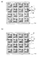
- FIGS. 1A to 1C are process diagrams showing an example of a method for producing a functional element of the present invention.
- FIGS. 1A to 1B correspond to cross-sectional views taken along the line XX in the schematic plan view of FIG. 1C, respectively.
- a functional layer forming coating solution 20 is applied in a pattern on the substrate 1, as shown in FIG. 1 (b).
- the functional layer 2 is formed.
- the functional layer 2 has a linear thin wire portion 2a and a wide area region 2b which is a region wider than the width of the thin wire portion 2a.
- the wide area region 2b is constituted by a plurality of wide area region constituting thin wires 2c having a width equal to the width of the thin wire portion 2a.
- the plurality of large area region constituting thin wires 2c are connected to each other and the thin wire portion 2a is connected. It is also characterized by the fact that they are also connected. Since the functional layer 2 has the above shape, as shown in FIGS.
- the application region G 2b corresponding to the wide area region 2b is changed to the application region G 2c corresponding to the wide area region constituting thin line 2c.
- Can be divided into it is possible to reduce the difference in the coating amount per unit area of the functional layer forming coating liquid 20 in the application region G 2b corresponding to the application region G 2a and wide area region 2b corresponding to the fine line portion 2a. Therefore, the film thickness unevenness of the functional layer 2 can be suppressed.
- a second functional layer 3 may be further formed in the present invention.
- the application region 3G corresponding to the second functional layer 3 is appropriately selected according to the thickness of the second functional layer 3 and the like.
- the functional element 10 can be manufactured by the above process.
- FIGS. 1B and 1C show an example in which the functional layer 2 is a conductive layer having conductivity and the functional element 10 is a TFT substrate.
- the functional layer 2 is a drain electrode
- the thin line portion 2a in the functional layer 2 is a linear conductive portion
- the large area region 2b in the functional layer 2 is a storage capacitor portion.
- An example is shown.
- the wide area region 2 b in the functional layer 2 is constituted by a wide area region constituting thin line 2 c in the plurality of functional layers 2.
- the second functional layer 3 is a source electrode is shown.
- FIGS. 3 (a) to 3 (b) are a schematic plan view and a schematic cross-sectional view showing another example of the method for producing a functional element of the present invention.
- FIGS. 3A to 3B are cross-sectional views taken along line XX of FIGS. 2A to 2B, respectively.
- a hydrophilic / hydrophobic pattern substrate 1a having a hydrophobic region A and a hydrophilic region B formed on its surface is prepared.
- the hydrophilic region B in the present invention includes a linear thin line portion B 2a and a wide area region B 2b that is wider than the width of the thin line portion B 2a .
- the wide area region B 2b is a thin line portion B.
- a plurality of wide area region constituting thin lines B 2c having a width equal to the width of 2a , and the plurality of large area region constituting thin lines B 2c are connected to each other and also connected to the thin line portion B 2a.
- the hydrophilic region B having at least the fine line portion B 2a and the large area region B 2b described above is formed.
- it may further have a second hydrophilic region 3B.
- the functional layer 2 and the second layer are formed by applying a functional layer forming coating solution onto the hydrophilic region B of the hydrophilic / hydrophobic pattern substrate 1a.
- the functional layer 3 is formed.
- the functional element 10 can be manufactured by the above process. 2B and 3B show an example in which the functional layer 2 is a conductive layer having conductivity and the functional element 10 is a TFT substrate. Further, the details of the functional layer 2 in FIGS. 2B and 3B can be the same as the contents described in FIGS. 1B and 1C, and thus the description thereof is omitted here. To do.
- the wide area region is constituted by a plurality of wide area region constituting thin wires having a width equal to the width of the thin wire portion, and the plurality of wide area region constituting thin wires are connected to each other and the thin wire
- a functional layer having a uniform thickness can be formed on the substrate. Therefore, the functional layer can be formed while suppressing the uneven thickness of the functional layer.
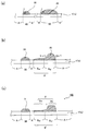
- the coating amount of the functional layer forming coating liquid per unit area applied to the coating area is: The larger the width of the coating area, the larger the thickness, and the thicker the functional layer obtained, the thicker the width of the coating area. More specifically, as shown in FIG. 11, since the contact angle ⁇ between the substrate 1 and the functional layer forming coating solution 20 is constant, the width is small when the widths of the coating regions 4G and 5G are different. The application amount of the functional layer forming coating solution 20 per unit area applied to the application region 5G having a width wider than that of the application region 4G increases.
- FIG. 11 is explanatory drawing explaining the relationship between the contact angle and coating amount of a coating liquid for a board
- the large area region 2′b is usually in a planar shape. It is formed.
- a functional layer having the above-described thin wire portion and a wide area region is formed using a functional layer forming coating solution, a difference in the thickness of the functional layer occurs due to the above-described width difference.
- the functional layer-forming coating liquid applied on the substrate usually has a property of gathering in a larger application amount due to surface tension. Therefore, as shown in FIG.
- FIG. 12 is a schematic plan view showing an example of a conventional functional element
- FIG. 13 is an explanatory diagram for explaining a functional layer forming coating solution in a conventional functional layer forming process
- FIG. 12 is a sectional view taken along line XX.
- the difference in thickness between the thin line portion and the large area in the functional layer becomes extremely large, for example, a portion where the thin line portion in the functional layer is too thin or not formed may occur. In this case, it may be difficult to exert the function of the functional layer in the thin line portion. Specifically, when the functional layer exhibits electrical conductivity, sufficient electrical conductivity cannot be exhibited in the thin line portion, which may cause electrical defects such as disconnection and short circuit.
- a coating method is used. When it is used, there is a problem that it may be difficult to form a coating film well, and when a printing method is used, for example, it may be difficult to print an accurate pattern.
- the present inventors as a functional layer design, when the functional layer has a linear thin line portion and a wide area region that is wider than the width of the thin line portion, the wide area region in the functional layer Is divided into a plurality of wide-area region-structured thin lines having a width equivalent to the width of the fine line portion of the functional layer, thereby making it possible to form the functional layer while suitably suppressing the uneven thickness of the functional layer.
- the headline and the present invention have been completed.
- the wide area region in the functional layer is constituted by a plurality of wide area region constituting thin lines having a width equivalent to the width of the thin line portion in the functional layer, and the plurality of wide area region constituting thin wires are respectively Are connected to each other and are also coupled to the thin line portion, so that the wide area region can be configured by a set of the plurality of wide area region constituting thin lines having a small width difference from the thin line portion.
- the difference in the application amount of the functional layer forming coating liquid per unit area applied to the application region corresponding to the part and the application region corresponding to the wide area region can be reduced, and the thin line part and the wide area in the functional layer can be reduced.
- the thickness of the region can be made uniform.
- the functional layer can be formed while suppressing the uneven thickness of the functional layer.
- the thickness of the fine line portion and the large area of the functional layer can be formed uniformly, for example, defects of the fine line portion in the functional layer can be prevented.
- a coating method when a coating method is used, a coating film can be formed satisfactorily, and when a printing method is used, for example, an accurate pattern can be printed well. can do.
- the functional layer formation process in this invention is a process of apply
- Substrate The substrate in the present invention is not particularly limited as long as the functional layer can be formed by applying a functional layer forming coating solution. Moreover, as a board
- Examples of the surface treatment include a hydrophilic / hydrophobic pattern treatment for forming a hydrophobic region and a hydrophilic region on the substrate surface, a surface unevenness treatment for forming surface unevenness on the substrate surface, and a self-assembled monomolecular film on the substrate surface.
- Chemical modification treatment for chemically modifying
- the substrate is preferably a hydrophilic / hydrophobic pattern substrate that has been subjected to hydrophilic / hydrophobic pattern processing.
- the functional layer can be formed with high definition by utilizing the difference in wettability between the hydrophilic region and the hydrophobic region.
- region can be formed by a simple method by apply
- hydrophobic / hydrophobic pattern substrate The hydrophilic / hydrophobic pattern substrate used in this step has a hydrophobic region and a hydrophilic region formed on the surface thereof.
- the functional layer forming coating liquid containing the functional layer material is applied only to the hydrophilic region by utilizing the wettability difference between the hydrophilic region and the hydrophobic region formed on the surface.
- patterning is performed. More specifically, patterning is performed by providing a difference in the contact angle of the functional layer forming coating solution between the hydrophilic region and the hydrophobic region.
- the contact angle with the functional layer forming coating solution is adjusted to be a constant value. Therefore, since the contact angles of the hydrophilic region and the functional layer forming coating liquid are constant, when the widths of the hydrophilic regions 4B and 5B are different as shown in FIG.
- the application amount of the functional layer forming coating solution 20 per unit area applied to the region 5B increases. Further, as shown in FIG. 15B, in the hydrophilic region B ′ having the thin line portion B 2′a and the wide area region B 2′b , the fine line is formed by the surface tension T of the functional layer forming coating solution 20. The functional layer forming coating solution 20 agglomerates from the part B 2′a toward the large area B 2′b . Therefore, even when the conventional functional layer 2 ′ is formed using the hydrophilic / hydrophobic pattern substrate 1a as shown in FIG. 15C, it is difficult to form the functional layer 2 ′ while suppressing the film thickness unevenness. is there.
- FIGS. 15A to 15C are explanatory views for explaining the hydrophilic / hydrophobic pattern substrate. Further, A in FIGS. 15B and 15C indicates a hydrophobic region.
- the hydrophobic region in the hydrophilic / hydrophobic pattern substrate used in this step is a region showing hydrophobicity
- the hydrophilic region is a region showing hydrophilicity.
- “hydrophobic” in the present invention refers to a case where the contact angle with water at 25 ° C. is 50 ° or more.
- “hydrophilic” in the present invention means that the contact angle of water at 25 ° C. is less than 50 °.
- the contact angle in the present invention is measured by, for example, dropping 1 microliter of liquid on a substrate, observing the shape of the dropped droplet from the side, and measuring the angle formed by the droplet and the substrate. can do.
- the contact angle in the present invention can be measured using, for example, a contact angle measuring device manufactured by Imoto Seisakusho. Further, the contact angle in the present invention can be measured using, for example, a contact angle meter DM-901 manufactured by Kyowa Interface Science.
- the hydrophobic region in the present invention is more preferable as the hydrophobicity is higher. More specifically, the hydrophobic region in the present invention is not particularly limited as long as the contact angle with water at 25 ° C. is 50 ° or more, but is preferably 70 ° or more, more preferably 80 ° or more. Further preferred.
- the hydrophilic region in the present invention is more preferable as the hydrophilicity is higher. More specifically, the hydrophilic region in the present invention is not particularly limited as long as the contact angle with water at 25 ° C. is less than 50 °, but is preferably 30 ° or less, more preferably 20 ° or less. Is more preferable.
- the difference between the contact angles in the hydrophilic region and the hydrophobic region in the present invention is preferably 10 ° or more, more preferably 40 ° or more, and further preferably 70 ° or more. preferable.
- the hydrophobicity of the hydrophobic region and the hydrophilicity of the hydrophilic region are higher, the difference in contact angle between the hydrophilic region and the hydrophobic region can be increased. Coloring can be performed with high definition. Therefore, a higher-definition functional layer can be formed.
- region in this invention is an area
- region in this invention is an area
- the wide area region is constituted by a plurality of wide area region constituting thin lines having a width equal to the width of the thin line portion.
- the large area of the hydrophilic region is provided so that the large area of the functional layer formed on the surface can exert its function.
- region of a functional layer can exhibit the function by forming in an area wider than a thin wire
- the function of the wide area region of the functional layer for example, the storage capacity of the drain electrode in the TFT substrate can be cited.
- the wide area region is a region wider than the width of the thin line portion. “The wide area region is a region wider than the width of the thin line portion” means that the width of the outer shape in a plan view of the wide area region in the direction perpendicular to the width direction of the thin line portion and the width in the width direction and horizontal direction of the thin line portion. It means that both of the widths of the outer shape in plan view of the area region are larger than the width of the thin line portion.
- the “width of the thin line portion” refers to the line width of the thin line portion formed in a linear shape, for example, the distance indicated by x1 in FIG.
- the “outer shape of the wide area region in plan view” refers to a shape formed by the outer periphery of the large area region. Further, when the plan view shape of the large area region has a gap portion F1 having an opening on the outer periphery of the large area region as shown in FIGS. 4A and 5A described later, the space between the openings is continuous. The shape formed by the outer periphery when it is assumed.
- the “outer shape in plan view of the wide area region” refers to, for example, a shape indicated by a broken line in FIGS. 4A and 5A, and more specifically, FIGS. 4B and 5B. The shape C surrounded by a solid line in FIG.
- the “notch portion of the planar view outer shape of the large area region” means a portion in which a part of the above figure is removed from the graphic including the planar view outer shape of the large area region, and more specifically, As shown in FIG. 4B, in the figure D including the outline shape C in plan view (the shape D surrounded by the alternate long and short dash line), a part E from which a part of the figure D is removed (the part E indicated by diagonal lines) ).
- the width of the outer shape in plan view of the wide area region in the direction perpendicular to the width direction of the thin line portion refers to a distance indicated by x2 in FIGS. 4A and 5A, for example.
- the width of the outer shape in plan view of the wide area region in the width direction and the horizontal direction of the thin line portion refers to, for example, a distance indicated by x3 in FIGS. 4 (a) and 5 (a).
- the “planar shape of the large area region” is a hydrophobicity disposed between the wide area region forming thin line formed in the large area region and the adjacent large area region disposed in the large area region.
- the “planar shape of the wide area region” means, for example, the wide area region constituting thin line B 2c in FIGS. 4 (a), 5 (a), 6 (a) to 6 (b), 7 and 8.
- interval part it may have an opening in the outer periphery of a large area area
- the “gap portion having an opening on the outer periphery of the large area region” refers to a gap portion having a portion continuous with the hydrophobic region located outside the large area region, and more specifically, FIG. ), A portion indicated by F1 in FIGS. 5 (a), 6 (a) to 6 (b) and FIG.
- the “gap portion having no opening on the outer periphery of the large area region” more specifically refers to a portion indicated by F2 in FIGS. 4 (a)-(b), FIGS. 5 (a)-(b), FIGS. 6 (a)-(b), FIG. 7 and FIG. 8 are used to explain examples of hydrophilic regions in the present invention.
- the wide area region is a region wider than the width of the thin line portion
- the wide area region means more specifically x2 and x3 in the hydrophilic region B shown in FIG. 4A, FIG. Both of the distances indicated by are larger than the distance indicated by x1.
- the ratio of the width of the planar view outer shape of the wide area region when the width of the thin line portion is 1 it can be appropriately selected according to the type of the functional element, and is not particularly limited. Especially, it is preferable that it is 5 or more, especially 10 or more.
- the ratio of the width of the planar area of the wide area region to the width of the thin line portion is less than the above-described range, it may be difficult to configure the wide area region with a plurality of wide area region configuration thin lines, This is because it may be difficult for the large area region to have a predetermined function when the large area region is constituted by a plurality of wide area region constituting thin lines.
- the specific width of the outer shape in plan view of the wide area region can be appropriately selected according to the type of the functional element of the present invention, and is not particularly limited.
- the width is in the range of 40 ⁇ m to 5000 ⁇ m. It is preferably in the range of 80 ⁇ m to 1000 ⁇ m, particularly in the range of 100 ⁇ m to 500 ⁇ m. This is because functional layers of various functional elements can be formed.
- the external shape of the wide area region in plan view can be appropriately selected according to the type of the functional element of the present invention, and is not particularly limited, but is preferably a square shape such as a square or a rectangle. This is because, when the outer shape of the large area area in plan view is a quadrangular shape, it can be satisfactorily constituted by a plurality of thin line portions. In this case, the outer shape of the wide area region in plan view may have a notch.
- the shape of the wide area region in plan view is appropriately determined according to the arrangement of a plurality of wide area region constituting thin lines described later.
- the shape of the wide area region in plan view may be any shape having a wide area region forming thin line and a gap, as shown in FIGS. 4 (a), 5 (a), and 6 (a) to 6 (b).
- the shape may have only the gap portion F1 having an opening on the outer periphery of the large area region B 2b , and only the gap portion F2 having no opening on the outer periphery of the large area region B 2b as shown in FIG.
- the shape may be sufficient, and as shown in FIG. 7, the shape which has both F1 and F2 may be sufficient.
- FIG. 7 the shape which has both F1 and F2 may be sufficient.
- a gap portion having an opening at least on the outer periphery of the wide area region B 2b Preferably, it has a shape having F1, and as shown in FIGS. 4 (a), 5 (a), and 6 (a) to 6 (b), only the gap portion F1 having an opening on the outer periphery of the large area B2b. It is preferable that it is a shape which has.
- the functional layer forming coating applied on the adjacent wide area region forming thin line
- the shape of the wide area region in plan view includes a shape including a stripe and a mesh shape.
- the wide area region is constituted by a plurality of wide area region constituting thin lines having a width equal to the width of the thin line portion.
- the plurality of wide area region constituting thin wires are connected to each other and also joined to the thin wire portion.
- the "plurality of large area region constituting thin lines are respectively connected", for example, wide area region thin lines adjacent in the plurality of large area regions constituting fine line B 2c1 ⁇ B 2c8 as shown in FIG. 4 (a) B 2c1 and B 2c2, coupled by B 2c2 and B 2c3, B 2c3 and B 2c4, B 2c4 and B 2c5, B 2c5 and B 2c6, B 2c6 and B 2C7, and B 2C7 and B 2C8 is large area extent configuration thin line B 2C9 Including cases where
- the wide area region constituting thin wire has the same width as the width of the thin line portion
- the difference between the width of the wide area region constituting thin line and the width of the thin line portion is applied to the functional layer forming coating. It means that the coating amount of the liquid is equal to the coating amount of the functional layer forming coating liquid applied to the wide area region constituting thin line.
- the amount of the functional layer forming coating liquid applied to the thin line portion is equal to the amount of the functional layer forming coating liquid applied to the wide area region constituting thin line”
- the difference in coating amount between the fine line portion and the large area region is due to the difference in thickness between the fine line portion and the large area region in the functional layer, which is caused by the movement of the coating liquid for forming the functional layer between the hydrophilic regions due to surface tension. The difference between the two functions is not inhibited.
- the ratio of the width of the wide area region constituting thin line to the width of the thin line portion is too large, even if the wide area region is constituted by a plurality of wide area region constituting thin lines, the thin line portion and the wide area in the functional layer This is because it may be difficult to sufficiently reduce the difference in thickness of the regions.
- the specific width of the wide area region constituting thin line can be appropriately selected according to the type of the functional layer forming coating solution, and is not particularly limited. For example, it is in the range of 2 ⁇ m to 200 ⁇ m, and in particular, 5 ⁇ m. It is preferable to be in the range of ⁇ 100 ⁇ m, particularly in the range of 10 ⁇ m to 40 ⁇ m. This is because the fine wire having a large area of the functional layer can be formed satisfactorily on the base material.
- the “width of the wide area region constituting thin line” means a line width of the wide area region constituting thin line formed in a linear shape, for example, a distance indicated by x4 in FIG.
- the length of the specific wide area region constituting thin line is appropriately selected according to the external shape of the wide area region in plan view.
- the arrangement of the plurality of wide area region constituting thin lines is appropriately selected according to the outer shape of the wide area region in plan view, and is not particularly limited, but the outer periphery of the wide area region is not closed by the wide area region constituting thin lines, In other words, the arrangement is preferably such that a gap having an opening is sandwiched around the outer periphery of the large area region.
- the arrangement of the plurality of wide area region constituting thin lines is such that the gap having openings at the outer periphery of the large area region is sandwiched.
- the functional layer forming coating liquid applied on the wire can be prevented from contacting at the gap, and a plurality of wide area region constituting fine lines in the functional layer can be arranged more finely so that the wide area region in the functional layer is formed. It is because it can form.
- the gap portion is formed by arranging the plurality of wide area region constituting thin lines in the above-described arrangement. The contact of the functional layer forming coating solution in can be suitably suppressed.
- the arrangement including the gap portion having the opening on the outer periphery of the wide area region is preferably an arrangement including a stripe arrangement, for example.
- a plurality of wide area region constituting thin lines are arranged in the width direction and the horizontal direction of the thin line portion B 2a.
- An arrangement in which B 2c is arranged in a stripe shape and the wide area region constituting fine lines B 2c adjacent to each other at one end of the stripe arrangement are combined, or the width direction of the fine line portion B 2a as shown in FIG.
- the width direction and the stripe arrangement in which a plurality of large area regions constituting thin line B 2c are arranged in the horizontal direction, the width direction and the vertical direction of the thin line portion B 2a of the fine line portion B 2a Alternatively, an array may be combined with a stripe array in which a plurality of wide area region forming thin lines B 2c are arrayed.
- the pitch width of the stripe arrangement can be appropriately selected according to the type of coating liquid for forming the functional layer, and is not particularly limited. It is preferably in the range of ⁇ 400 ⁇ m, in particular in the range of 10 ⁇ m to 200 ⁇ m, particularly in the range of 20 ⁇ m to 80 ⁇ m. This is because, when the pitch width of the stripe arrangement is too narrow, adjacent wide area region constituting fine lines may come into contact with each other in the hydrophobic region. Moreover, it is because it may become difficult to provide a predetermined function to a wide area area
- the pitch width of the stripe arrangement refers to the distance between the centers of adjacent wide area region constituting thin wires, for example, the distance indicated by x5 in FIG.
- the interval between the stripe arrangements can be appropriately selected according to the type of the functional layer forming coating solution, and is not particularly limited. It is preferably in the range of 200 ⁇ m, especially in the range of 5 ⁇ m to 100 ⁇ m, particularly in the range of 10 ⁇ m to 40 ⁇ m. This is because if the stripe arrangement interval is too narrow, adjacent wide-area region constituting fine lines may come into contact with each other in the hydrophobic region. If the stripe arrangement interval is too wide, a predetermined large area region is set. This is because it may be difficult to provide this function.
- the interval between the stripe arrangements means a distance between adjacent wide area region forming thin lines, for example, a distance indicated by x6 in FIG.
- an array of a plurality of wide area region constituting thin lines an array in which the outer periphery of the wide area region is closed by the wide area region constituting thin lines, that is, an array having a gap portion having no opening on the outer periphery of the large area region.
- An arrangement in which the gaps F2 having no gaps are sandwiched can be given.
- the width, pitch width, and interval between the wide area region constituting thin lines can be the same as those of the array including the stripe arrangement described above, and thus the description thereof is omitted here. .
- the area in which the wide area region constituting thin line is formed in the wide area region (hereinafter, may be referred to as the area of the wide area region constituting thin line) is as long as the function of the wide area region can be secured. It does not specifically limit and can be suitably selected according to the kind of functional element.
- the ratio of the area of the wide area region constituting thin wire to the area of the entire large area region is in the range of 0.10 to 0.95, in particular in the range of 0.30 to 0.90, particularly 0. It is preferably in the range of 40 to 0.70.
- the ratio of the area of the wide area region constituting thin wire is too large, it is not possible to sufficiently secure a gap portion disposed between each wide area region constituting thin wire, and the functional layer forming coating solution is applied. This is because there is a possibility that the functional layer forming coating liquid applied on the adjacent wide area region constituting thin wires may come into contact with the gap portion.
- the area ratio of the above-mentioned wide area region constituting thin wire is small, other layers can be formed on the wide area region of the functional layer to ensure the function of the large area region, From the viewpoint of safety, it is preferable that the area ratio of the wide area region constituting thin wires is adjusted so as to be formed as a single layer.
- Fine wire portion The fine wire portion in the present invention is formed in a linear shape and is coupled to the above-described wide area region constituting fine wire.
- the specific width of the thin wire portion can be made equal to the width of the above-described wide area region constituting thin wire, description thereof is omitted here.
- the length of the thin wire portion, the shape in plan view, and the like are appropriately selected according to the type of functional element.
- the “length of the thin line portion” refers to a distance indicated by x7 in FIG.
- (B) Second hydrophilic region The hydrophilic / hydrophobic pattern substrate used in this step only needs to have a hydrophilic region having a fine line portion and a wide area, and for example, FIG. 2 (a) and FIG. As shown to 3 (a), the 2nd hydrophilic region 3B which has only a thin wire
- variety of a 2nd hydrophilic region since it can be made equal to the width
- hydrophobic region in the present invention is usually formed in a region other than the hydrophilic region and the second hydrophilic region formed as necessary on the surface of the hydrophilic / hydrophobic pattern substrate.
- Such a hydrophilic / hydrophobic pattern substrate has a structure in which a hydrophilic region is formed in a desired pattern on the surface of the hydrophobic substrate including a hydrophobic material (the hydrophilic / hydrophobic pattern substrate of the first aspect) and A hydrophilic substrate having a hydrophilic surface and a hydrophobic layer formed on the hydrophilic substrate and having hydrophobic properties, the hydrophobic layer being removed in a pattern, and the surface of the hydrophilic substrate being patterned And the one having a configuration exposed in a shape (the hydrophilic / hydrophobic pattern substrate of the second embodiment).
- the hydrophilic / hydrophobic pattern substrate of each of these embodiments will be described.
- Hydrophilic / hydrophobic pattern substrate of the first aspect has a structure in which a hydrophilic region is formed in a desired pattern on the surface of the hydrophobic substrate whose surface contains a hydrophobic material. It is.
- the hydrophobic substrate in this embodiment may be any substrate as long as at least the surface thereof contains a hydrophobic material capable of imparting hydrophilicity by performing a predetermined hydrophilic treatment.
- the hydrophobic substrate itself is hydrophobic. It may be made of a material, or may be one in which a layer containing a hydrophobic material is formed on a hydrophilic substrate such as glass, SiO 2 , SiN, or SiON.
- the hydrophobic material in this embodiment may be an organic material or an inorganic material.
- examples of the hydrophobic material used for the hydrophobic substrate in this embodiment include polystyrene, polyimide, polyester, polyethylene, polyphenylene sulfide, polyparaxylene, polyethylene terephthalate, polyethylene naphthalate, and polydimethylsiloxane.
- any of these hydrophobic materials can be suitably used.
- only a single type of hydrophobic material may be used, or a plurality of types of hydrophobic materials may be used.
- the thickness of the hydrophobic substrate in this embodiment is within a range in which desired self-supporting property, flexibility, and the like can be imparted to the hydrophobic substrate according to the use of the functional element of the present invention. It is not particularly limited. In particular, the thickness of the hydrophobic substrate in this embodiment is preferably in the range of 1 ⁇ m to 5 mm, more preferably in the range of 10 ⁇ m to 1.5 mm, and in the range of 25 ⁇ m to 1.0 mm. Is more preferable.
- Examples of the method for forming the hydrophilic / hydrophobic pattern substrate of this embodiment include a method of forming a patterned hydrophilic region on the hydrophobic substrate of this embodiment. More specifically, the surface of the hydrophobic substrate is patterned.
- the method of hydrophilizing can be mentioned.
- the method for hydrophilizing the surface of the hydrophobic substrate is not particularly limited as long as it is a processing method capable of forming a hydrophilic region having a desired hydrophilicity depending on the type of hydrophobic material constituting the hydrophobic substrate. Is not to be done.
- Examples of such a method include a method of irradiating the surface of the hydrophobic substrate with ultraviolet rays, an electron beam or a laser through a photomask, or an active radiation such as ultraviolet rays directly in a pattern on the surface of the hydrophobic substrate.
- the method etc. which irradiate can be mentioned.
- the hydrophobic material used for the hydrophobic substrate has the property of being partially decomposed by irradiation with ultraviolet rays or the like to generate OH groups
- the surface of the hydrophobic substrate is irradiated with ultraviolet rays in a pattern. By doing so, it is possible to form a hydrophilic region that is made hydrophilic by generating OH groups on the surface.
- hydrophilic / hydrophobic pattern substrate of the second aspect includes a hydrophilic substrate having a hydrophilic surface and a hydrophobic layer formed on the hydrophilic substrate and exhibiting hydrophobicity. The hydrophobic layer is removed in a pattern, and the surface of the hydrophilic substrate is exposed in a pattern.
- hydrophilic substrate The material constituting the hydrophilic substrate used for the hydrophilic / hydrophobic pattern substrate of the second aspect (hereinafter referred to as “hydrophilic material”) is not particularly limited as long as it can produce a hydrophilic substrate having desired hydrophilicity. It is not a thing. Therefore, the hydrophilic material used in this embodiment may be an inorganic material or an organic material. Examples of such a hydrophilic material include glass, SiO 2 , SiN, and SiON.
- a hydrophobic substrate including a hydrophobic material such as polyimide, polyester, polyethylene, polyphenylene sulfide, or polyparaxylene is subjected to a hydrophilic treatment using ultraviolet light, electron beam, laser, or the like.
- a hydrophilic treatment using ultraviolet light, electron beam, laser, or the like can be mentioned.
- any hydrophilic substrate made of any of these hydrophilic materials can be preferably used.
- the hydrophobic substrate is hydrophilized using ultraviolet light, electron beam, laser, or the like. It is preferable to use one that has been treated.
- the thickness of the hydrophilic substrate used for the hydrophilic / hydrophobic pattern substrate of the second aspect desired self-supporting property, flexibility, etc. are imparted to the hydrophilic substrate according to the use of the functional element of the present invention. If it is in the range which can do, it will not specifically limit.
- the thickness of the hydrophilic substrate used in this embodiment is preferably in the range of 1 ⁇ m to 5 mm, more preferably in the range of 10 ⁇ m to 1.5 mm, and in the range of 25 ⁇ m to 1.0 mm. More preferably it is.
- the hydrophobic layer used in the hydrophilic / hydrophobic pattern substrate of the second embodiment is not particularly limited as long as it has the above hydrophobic property, but among them, one that can be removed in a pattern is preferable.
- the hydrophobic layer used in this embodiment is preferably a self-assembled monolayer made of a self-assembled monolayer material. This is because when the hydrophobic layer is a self-assembled monomolecular film, it becomes easy to remove the hydrophobic layer in a high-definition pattern.
- the self-assembled monolayer material is not particularly limited as long as it can form a hydrophobic layer made of a self-assembled monolayer having a desired hydrophobicity.
- self-assembled monolayer materials include HMDS (hexamethyldisilazane), OTS (octyltrichlorosilane), ODTS (octadecyltrichlorosilane), FAS (fluorinated alkylsilane), alkyltrimethoxysilane. And alkyltriethoxysilane.
- any of these self-assembled monolayer materials can be suitably used.
- HMDS hexamethyldisilazane
- OTS octyltrichlorosilane
- ODTS octadecyltrichlorosilane
- the thickness of the hydrophobic layer is not particularly limited and can be appropriately determined according to the material used for forming the hydrophobic layer.
- the hydrophilic substrate in the second embodiment can produce a hydrophilic / hydrophobic patterned substrate by removing the hydrophobic layer in a pattern, the thickness of the hydrophobic layer is removed in a pattern. It is preferable that it is easy to do.
- the thickness of the hydrophobic layer used in this embodiment is preferably in the range of 0.1 nm to 1 ⁇ m, more preferably in the range of 0.1 nm to 100 nm, and 0.1 nm More preferably, it is in the range of ⁇ 10 nm.
- Method for forming hydrophilic / hydrophobic pattern substrate As a method for forming the hydrophilic / hydrophobic pattern substrate of this embodiment, for example, when the above-described hydrophilic substrate is used, the hydrophobic layer is removed in a pattern and the surface of the hydrophilic substrate is exposed in a pattern. be able to.
- the hydrophobic layer is formed according to the configuration of the hydrophobic layer. There is no particular limitation as long as it can be removed. However, in this method, since the hydrophilic region is formed by exposing the surface of the hydrophilic substrate, the method of removing the hydrophobic layer is a method that can remove the hydrophobic layer almost completely. It is preferable.
- the surface of the hydrophobic layer is irradiated with ultraviolet rays through a photomask to decompose and remove the hydrophobic layer, or the surface of the hydrophobic layer is exposed to ultraviolet rays, electron beams, plasma, etc.
- Examples of the method of irradiating the active radiation in a pattern include a method of decomposing and removing the hydrophobic layer.
- both the hydrophilic / hydrophobic pattern substrate of the first aspect and the hydrophilic / hydrophobic pattern substrate of the second aspect described above can be used, but it is more preferable to use the hydrophilic / hydrophobic pattern substrate of the second aspect.
- a hydrophobic layer made of a self-assembled monolayer is formed in the region. Since the hydrophobic layer made of a self-assembled monolayer can be easily removed in a pattern by ultraviolet irradiation or the like, a hydrophilic / hydrophobic pattern substrate having a high-definition hydrophilic region and a hydrophobic region pattern can be obtained. Because.
- the substrate used in this step is not limited to the hydrophilic / hydrophobic pattern substrate, and can be appropriately selected according to the type of functional element.
- a general glass substrate or resin substrate can be used.
- substrate what has a sheet form, a film form, and a plate-shaped form can be used.
- the functional layer forming coating liquid used in this step usually contains a functional layer material and a solvent.
- the material for the functional layer can be appropriately selected according to the type of the functional element, and is not particularly limited.
- the material for the functional layer is preferably a conductive material.
- a conductive layer having conductivity can be formed as the functional layer, and unevenness of the film thickness of the conductive layer can be suppressed, so that occurrence of electrical defects such as disconnection and short circuit in the thin wire portion can be suppressed. .
- region in a conductive layer can be made uniform, it can be set as the conductive layer which shows favorable electroconductivity.
- the conductive material include metal particles or metal oxide particles such as Au, Cu, Ag, ITO, and Pt, carbon materials such as graphene and carbon nanotubes, and conductive polymer materials such as PEDOT / PSS. .
- Examples of the solvent in the functional layer-forming coating solution include water, acetone, methanol, ethanol, isopropyl alcohol, propylene glycol 1-monomethyl ether 2-acetate, toluene, xylene, mesitylene, tetralin, decahydronaphthalene, chlorobenzene, dibenzene, and the like. And chlorobenzene.
- a coating liquid for forming a functional layer is applied onto a substrate to form a thin line portion and a wide area region having a plurality of wide area region constituting thin lines.
- the functional layer can be formed.
- a method of applying a functional layer forming coating solution in a pattern can be mentioned, and specific examples include an ink jet method and a nozzle jet method.
- a functional layer forming coating solution is applied onto the hydrophilic region of the hydrophilic / hydrophobic pattern substrate.
- the method for applying the functional layer forming coating solution on the hydrophilic / hydrophobic pattern substrate is particularly limited as long as it is a method capable of forming a coating film of the functional layer forming coating solution on the hydrophilic region of the hydrophilic / hydrophobic pattern substrate. Is not to be done.
- a method of applying the functional layer forming coating solution a method of applying to the entire surface of the hydrophilic / hydrophobic pattern substrate is preferably used.
- the functional layer can be formed by a simple method because the coating liquid for forming the functional layer can be selectively applied to the hydrophilic region by utilizing the difference in hydrophilicity and hydrophobicity on the surface of the hydrophilic / hydrophobic pattern substrate. Because you can.
- coating methods include generally known methods such as spin coating, capillary coating, die coating, roll coating, bar coating, dip coating, spray coating, blade coating, and gravure offset printing.
- the coating method can be used.
- a method of applying the functional layer forming coating solution onto the hydrophilic / hydrophobic pattern substrate a method of applying the above-described functional layer forming coating solution in a pattern can also be used.
- the functional layer formed in this step is formed on the substrate described above.
- the functional layer has a thin line portion and a wide area region composed of a plurality of wide area region constituting thin lines.
- the thin line portion, the wide area region, and the wide area region constituting thin line can be the same as those described in the above-mentioned section of “1.
- the thickness of the functional layer is appropriately selected according to the type of the functional element of the present invention, and is not particularly limited. For example, it can be set to about 30 nm to 500 nm.
- the functional layer in the present invention has the above-described wide area region, the difference between the thickness of the thin line portion and the thickness of the wide area region in the functional layer is reduced, and the thickness of the functional layer is made uniform. be able to. More specifically, the absolute value of the difference between the thickness of the fine line portion and the thickness of the large area in the functional layer is 200 nm or less, preferably 100 nm or less, and particularly preferably 30 nm or less. preferable.
- the absolute value of the difference between the thickness of the fine line portion in the functional layer and the thickness of the wide area region is large, for example, it may be difficult to exhibit predetermined conductivity in the fine line portion in the functional layer, or for example, the functional layer This is because it may be difficult to satisfactorily form another layer on the large area region.
- the thickness of the thin line portion in the functional layer and the thickness of the wide area region can be measured by, for example, Surfcoder SE4000 manufactured by Kosaka Laboratory Ltd.
- the thickness of the wide area region in the functional layer is the average value obtained by measuring the thickness of each of the plurality of wide area region constituting thin wires constituting the wide area region and averaging the obtained measurement values. To do.
- the functional layer in the present invention is not particularly limited as long as it has the fine line portion and the large area described above.
- the drain electrode in the substrate for TFT illustrated in FIG. When the functional layer is the drain electrode, for example, the linear conductive portion corresponds to a thin line portion, and the storage capacitor portion corresponds to a wide area region.
- examples of the functional layer include a wiring layer and a sensor unit in the touch panel sensor illustrated in FIGS. 9 to 10.
- FIG. 9 is a schematic plan view showing another example of the functional element manufactured according to the present invention
- FIG. 10 is a sectional view taken along line XX of FIG. 9 and 10 show an example in which the functional element 10 is a projected capacitive touch panel sensor.
- the touch panel sensor shown in FIG. 9 and FIG. 10 includes an insulating base material 11, a sensor portion 23 formed on the insulating base material 11, and a wiring layer 24.
- the sensor unit 23 is formed in the active area of the touch panel sensor, and usually the sensor electrode having the first electrode 21b and the second electrode 22b and the first conductive unit 21a and the second electrode 22b that connect the first electrode 21b to each other. And a conductive portion having a second conductive portion 22a for connecting the two.
- the wiring layer 24 includes a lead-out wiring 24a formed outside the active area and connected to the sensor electrode, and an external connection terminal 24b connected to the lead-out wiring 24a. 9 and 10, the first electrode 21b, the first conductive portion 21a, the lead wire 24a connected to the first electrode 21b and the external connection terminal 24b on the two insulating base materials 11, respectively.
- the second electrode 22b, the second conductive portion 22a, the lead wire 24a connected to the second electrode 22b, and the external connection terminal 24b are formed, and the two insulating base materials 11 are bonded together with the insulating layer 4 interposed therebetween.
- An example is shown.
- the functional layer 2 in the present invention is the wiring layer 24 described above
- the insulating substrate 11 corresponds to the hydrophilic / hydrophobic pattern substrate 1a
- the lead-out wiring 24a corresponds to the thin wire portion 2a
- the external connection terminal 24b corresponds to the wide area region 2b. It corresponds to.
- the insulating base material 11 corresponds to the hydrophilic / hydrophobic pattern substrate 1a
- the first conductive portion 21a and the second conductive portion 22a correspond to the thin wire portion 2a
- the first electrode 21b and the second electrode 22b correspond to the wide area region 2b.
- the sensor electrode, conductive portion, lead-out wiring, external connection terminal, and other aspects of the touch panel sensor and other details of the touch panel sensor can be the same as those of a general touch panel sensor, for example, Japanese Patent Laid-Open No. 2013-210732 Since it can be the same as that described in JP 2013-210733 A, description thereof is omitted here.
- a wiring layer in a display panel can be cited.
- the wiring layer can be the same as that used for a general display panel, and usually has a lead-out wiring and an external connection terminal.
- the lead-out wiring corresponds to the thin line portion
- the external connection terminal corresponds to the wide area region.
- the functional layer forming step in the present invention may be performed as long as the functional layer can be formed on the substrate.
- the hydrophilic / hydrophobic pattern substrate has the second hydrophilic region
- the second function is formed on the second hydrophilic region. Layers can be formed simultaneously.
- Examples of the second functional layer formed on the second hydrophilic region include a source electrode on a TFT substrate and a pixel electrode on a display panel substrate.
- the method for producing a functional element of the present invention is not particularly limited as long as it has the functional layer forming step described above, and other steps can be appropriately selected and added as necessary. Examples of such a process include a process of forming a hydrophilic / hydrophobic pattern substrate and a process of forming with another layer on the functional layer.
- the functional element produced according to the present invention is not particularly limited as long as it has the above-described functional layer. Examples thereof include a TFT substrate, a touch panel sensor, and a display panel substrate.
- the touch panel sensor has two insulating bases as shown in FIGS. 9 and 10
- the touch panel member having the insulating base on which each conductive portion and sensor electrode are formed is also a functional element. be able to.
- the manufacturing method of the TFT substrate of the present invention is the above-described “A. Functional element manufacturing method”, in which the functional layer is a conductive layer having conductivity, and the conductive layer is a TFT.
- This is a manufacturing method characterized by being a part of the structure. That is, the TFT substrate manufacturing method of the present invention is a manufacturing method having a conductive layer forming step of forming a conductive layer having conductivity by applying a conductive layer forming coating solution containing a conductive material on the substrate.
- the conductive layer has a linear thin line portion and a wide area region that is wider than the width of the thin line portion, and the wide area region has a width equivalent to the width of the thin line portion.
- the manufacturing method is characterized in that the plurality of wide area region constituting thin lines are connected to each other and are also coupled to the thin line portion.
- FIGS. 1A to 1C, FIGS. 2A to 2B, and FIGS. 3A to 3B are schematic plan views showing an example and another example of a method for manufacturing a TFT substrate of the present invention.
- FIG. Details of FIGS. 1A to 1C, FIGS. 2A to 2B, and FIGS. 3A to 3B are described above in the section “A. Functional element manufacturing method”. Therefore, the description is omitted here.
- the wide area region is constituted by a plurality of wide area region constituting thin wires having a width equal to the width of the thin wire portion, and the plurality of wide area region constituting thin wires are connected to each other and the thin wire
- a conductive layer having a uniform thickness can be formed on the substrate. Therefore, the conductive layer can be formed while suppressing unevenness in the thickness of the conductive layer. That is, in the present invention, the conductive layer which is a part of the structure of the thin film transistor can be formed while suppressing unevenness in film thickness.
- the conductive material and solvent used in the conductive layer forming coating solution, the coating method, and the conductive layer the above-mentioned “A. Functional element manufacturing method” Since it can be the same as that described in the section, description thereof is omitted here.
- the functional element of the present invention has a substrate and a functional layer formed on the substrate, and the functional layer has a linear fine line portion and a width of the fine line portion.
- a wide area that is a wide area, and the wide area area is configured by a plurality of wide area area configuration thin lines having a width equal to the width of the thin line portion, and the plurality of wide area area configuration thin lines are These are connected to each other and are also connected to the thin line portion.
- FIG. 1 (b), (c), FIG. 2 (b) and FIG. 3 (b), and FIG. 9 and FIG. 10 are schematic plan views and sectional views showing an example of the functional element of the present invention and other examples. is there. Note that the details of these drawings can be the same as the contents described in the section “A. Functional element manufacturing method”, and thus the description thereof is omitted here.
- the functional layer having a uniform thickness can be formed by having the above-described wide area region, it is possible to obtain a functional element in which the thickness unevenness of the functional layer is suppressed.
- the fine line portion the wide area region and the wide area region constituting thin line in the functional layer, the thin line portion, the wide area region and the wide area region constitution in the hydrophilic region described in the above-mentioned section of “A. Since it can be the same as that of a thin wire
- the configuration of the functional element of the present invention can be the same as the content described in the above-mentioned section “A. Functional element manufacturing method”, and thus the description thereof is omitted here.
- the TFT substrate of the present invention is such that, in the above-mentioned “C. Functional element”, the functional layer is a conductive layer having conductivity, and the conductive layer is part of the structure of the TFT. It is characterized by. That is, the TFT substrate of the present invention includes a substrate and a conductive layer having conductivity formed on the substrate, and the conductive layer includes a linear thin wire portion and the thin wire portion. A wide area region that is wider than the width of the thin line portion, and the wide area region is configured by a plurality of wide area region configuration thin wires having a width equal to the width of the thin wire portion, and the plurality of wide area regions The constituent thin wires are connected to each other and are also connected to the thin wire portion.
- FIGS. 1B, 1C, 2B, and 3B are a schematic plan view and a cross-sectional view showing an example of a TFT substrate of the present invention. Note that the details of these drawings can be the same as the contents described in the section “A. Functional element manufacturing method”, and thus the description thereof is omitted here.
- the conductive layer having a uniform thickness can be formed by having the above-described wide area region, a thin film transistor substrate in which unevenness in the thickness of the conductive layer is suppressed can be obtained. That is, in the present invention, the conductive layer can have a nonuniform thickness, and can be suitably used as part of the structure of the thin film transistor.
- the configuration of the TFT substrate of the present invention can be the same as that described in the above-mentioned section “A. Method for manufacturing functional element”, and thus the description thereof is omitted here.
- the present invention is not limited to the above embodiment.
- the above-described embodiment is an exemplification, and the present invention has substantially the same configuration as the technical idea described in the claims of the present invention, and any device that exhibits the same function and effect is the present invention. It is included in the technical scope of the invention.
- Example 1 (Production of metal mask) A metal mask having an opening corresponding to the shape of the source / drain electrode illustrated in FIG. In the opening of the metal mask, the line width corresponding to B 2a of the drain electrode in FIG. 2A is 20 ⁇ m, and the line width corresponding to B 2c is 20 ⁇ m.
- the details of the shape of the opening corresponding to the drain electrode of the metal mask in plan view are the same as the shape of the drain electrode described later in plan view.
- Styrene polymer (Wako Pure Chemical Industries) was dissolved in propylene glycol 1-monomethyl ether 2-acetate (Kanto Kagaku Special Grade) at a concentration of 5 wt% to obtain a styrene polymer solution.
- the styrene polymer solution was applied onto a glass substrate with a spin coater (Mikasa MS-A100) and heated with a hot plate (As One ND-1) at 120 ° C. to form a polystyrene film on the glass substrate.
- Nano Ag colloid (Sigma-Aldrich 730785) was applied to the polystyrene surface of the hydrophilic / hydrophobic pattern substrate with a bar coat (Kobayashi M50), and pattern formation of the Ag layer was performed by the hydrophilic / hydrophobic effect.
- This substrate was baked on a hot plate at 150 ° C. for 1 hour. Through the above procedure, a TFT substrate having a source / drain electrode having a planar view shape illustrated in FIG. 2 was produced.
- the distance corresponding to x1 is 20 ⁇ m
- the distance corresponding to x2 is 300 ⁇ m
- the distance corresponding to x3 is 300 ⁇ m
- the distance corresponding to x4 is 20 ⁇ m.
- the distance corresponding to x5 was 40 ⁇ m
- the distance corresponding to x6 was 20 ⁇ m
- the distance corresponding to x7 was 180 ⁇ m.
- the thickness of the drain electrode (Ag layer) was measured with a surf coder SE4000 manufactured by Kosaka Laboratory
- the thickness of the thin line portion (2a in FIG. 3B) was 140 nm ⁇ 12 nm over a wide area region ( In FIG. 3B, the thickness of 2b) (the plurality of wide area region constituting thin lines (average of the thickness of 2c in FIG. 3B)) is 150 nm ⁇ 4 nm, and the difference in thickness between the two is 10 nm.
- Example 2 A TFT substrate was prepared in the same manner as in Example 1 except that the following metal mask was prepared and used.
- the line width corresponding to B 2a in FIG. 2A was 20 ⁇ m
- the line width corresponding to B 2c was 10 ⁇ m.
- the details of the shape of the opening corresponding to the drain electrode of the metal mask in plan view are the same as those of the drain electrode described later.
- the distance corresponding to x1 is 20 ⁇ m
- the distance corresponding to x2 is 150 ⁇ m
- the distance corresponding to x3 is 150 ⁇ m
- the distance corresponding to x4 is 10 ⁇ m.
- the distance corresponding to x5 was 20 ⁇ m
- the distance corresponding to x6 was 10 ⁇ m
- the distance corresponding to x7 was 110 ⁇ m.
- the thickness of the obtained drain electrode was measured by the same measuring method as in Example 1
- the thickness of the thin line portion (2a in FIG. 3B) was 140 nm ⁇ 12 nm over a wide area region ( In FIG.
- the thickness of 2b) (the plurality of wide area region constituting thin wires (average of the thickness of 2c in FIG. 3 (b)) is 270 nm ⁇ 15 nm, and the difference in thickness between the two is 130 nm.
- Example 3 A TFT substrate was prepared in the same manner as in Example 1 except that the following metal mask was prepared and used.
- the line width corresponding to B 2a in FIG. 2A was 20 ⁇ m
- the line width corresponding to B 2c was 40 ⁇ m.
- the details of the shape of the opening corresponding to the drain electrode of the metal mask in plan view are the same as those of the drain electrode described later.
- the distance corresponding to x1 is 20 ⁇ m
- the distance corresponding to x2 is 440 ⁇ m
- the distance corresponding to x3 is 440 ⁇ m
- the distance corresponding to x4 is 40 ⁇ m.
- the distance corresponding to x5 was 60 ⁇ m
- the distance corresponding to x6 was 20 ⁇ m
- the distance corresponding to x7 was 340 ⁇ m.
- the thickness of the obtained drain electrode was measured by the same measuring method as in Example 1
- the thickness of the thin line portion (2a in FIG. 3B) was 140 nm ⁇ 12 nm over a wide area region ( In FIG.
- the thickness of 2b) (the plurality of wide area region constituting thin wires (average of the thickness of 2c in FIG. 3B) is 60 nm ⁇ 3 nm, and the difference in thickness between the two is as follows: , 80 nm.
- Example 1 (Production of hydrophilic / hydrophobic pattern substrate) A TFT substrate was produced in the same manner as in Example 1 except that a metal mask having an opening corresponding to the shape of the source / drain electrode in plan view (FIG. 21) not including the wide area region constituting thin line was produced. did. The details of the shape of the opening corresponding to the drain electrode of the metal mask in plan view are the same as those of the drain electrode described later.
- the width of the fine line portion, the length of the fine line portion, the width of the outer shape in a plan view of the wide area in the direction perpendicular to the width direction of the fine line portion, the width direction of the fine line portion The width of the outer shape in plan view of the large area in the horizontal direction was the same as in Example 1.
- the thickness of the drain electrode (Ag layer) was measured in the same manner as in Example 1, the thin line portion (2′a in FIG. 15C) had a large area region (FIG. 15) with respect to 70 nm ⁇ 10 nm.
- the thickness of 2′b) was 2.1 ⁇ m ⁇ 0.1 ⁇ m, and the thickness of the wide area region was 20 times or more the thickness of the thin wire portion.
- Example 4 A hydrophilic / hydrophobic pattern substrate was produced in the same manner as in Example 1. Apply nano-Ag colloid (Sigma-Aldrich 730785) to polystyrene surface of hydrophilic / hydrophobic pattern substrate using inkjet device (Fujifilm, Dimatics Material Printer DMP-3000), and pattern formation of Ag layer by hydrophilic and hydrophobic effect went. This substrate was baked on a hot plate at 150 ° C. for 1 hour. A TFT substrate was produced by the above procedure. In the drain electrode of the obtained TFT substrate, the distance corresponding to x1 to x7 in FIG. 4A was the same as the distance corresponding to x1 to x7 in Example 1.
- the thickness of the drain electrode (Ag layer) was measured in the same manner as in Example 1, the thickness of the thin line portion (2a in FIG. 3B) was 140 nm ⁇ 5 nm with respect to the wide area region (FIG. 3 ( In b), the thickness of 2b) (a plurality of wide area region constituting thin wires (average of the thickness of 2c in FIG. 3B) is 150 nm ⁇ 10 nm, and the difference between the thicknesses is 10 nm. there were.
- Example 5 A TFT substrate was produced in the same manner as in Example 4 except that the shape of the opening corresponding to the drain electrode of the metal mask and the shape of the drain electrode were the shapes shown in FIG. The details of the shape of the opening corresponding to the drain electrode of the metal mask in plan view are the same as those of the drain electrode described later.
- the distance corresponding to x1 to x7 in FIG. 8 was the same as the distance corresponding to x1 to x7 in Example 1.
- the thickness of the drain electrode (Ag layer) was measured in the same manner as in Example 1, the thickness of the thin line portion (2a in FIG. 3B) was 140 nm ⁇ 5 nm with respect to the wide area region (FIG.
- the thickness of 2b) (the plurality of wide area region constituting thin wires (average of the thickness of 2c in FIG. 3B)) is 146 nm ⁇ 5 nm, and the difference between the thicknesses is 6 nm. there were.
- Comparative Example 2 The same as Comparative Example 1 except that nano Ag colloid (Sigma-Aldrich 730785) was applied to the polystyrene surface of the hydrophilic / hydrophobic pattern substrate using an inkjet device (Fujifilm, Dimatics Material Printer DMP-3000). A TFT substrate was prepared by the method.
- the thickness of the drain electrode (Ag layer) was measured in the same manner as in Example 1, the thin line portion (2′a in FIG. 15C) had a wide area region (FIG. 15) with respect to 90 nm ⁇ 15 nm.
- the thickness of 2′b) was 2.0 ⁇ m ⁇ 100 nm, and the thickness of the wide area region was 20 times or more the thickness of the thin line portion.
- Table 1 below shows the form and the like of the drain electrode in the TFT substrates of Examples 1 to 5 and Comparative Examples 1 and 2.
- “20 times or more” indicates that the thickness of the wide area region is 20 times or more the thickness of the thin line portion. .
- TFT characteristics Using the TFT substrates of Examples 1 to 5 and Comparative Examples 1 and 2, TFTs were produced by the following procedure, and TFT characteristics were measured.
- An organic semiconductor solution (Sigma-Aldrich Plexcore OS2100) was spin-coated on the channel portion of the source / drain electrode of the TFT substrate of Examples 1 to 5 and Comparative Examples 1 and 2 to form an organic semiconductor layer.
- a gate insulating layer was formed by forming a polystyrene solution on the surface as described above, and Al was vacuum-deposited as a gate electrode to form a top gate type thin film transistor.
- 20 thin film transistors are arranged on the same substrate. As a result of measuring these transistor characteristics, in Examples 1 to 5, all of the 20 transistors operated normally, and the mobility showed a range of 0.01 cm 2 /Vs ⁇ 0.004 cm 2 / Vs. It was.
- Comparative Example 1 As a result of measuring the transistor characteristics, only three of the 20 thin film transistors operated. Also in Comparative Example 2, when the transistor characteristics were measured, those that did not operate were included. This is because conduction is not possible due to insufficient thickness of the thin wire portion, and charge cannot be injected into the semiconductor. From this result, it was clearly shown that it is difficult to simultaneously form the thin line portion and the wide area region by the hydrophilic / hydrophobic effect.
- Example 6 In the same manner as in Example 1, a polystyrene film was formed on a glass substrate. A nano Ag colloid (Sigma-Aldrich 730785) is formed on the surface of the polystyrene film without forming a hydrophilic / hydrophobic pattern, as in Example 1 using an inkjet apparatus (Fujifilm, Dimatics Material Printer DMP-3000). It apply
- the thickness of the drain electrode (Ag layer) obtained was measured in the same manner as in Example 1, the thin line portion (2a in FIG. 1 (b)) had a wide area ( In FIG. 1B, the thickness of 2b) (a plurality of wide area region constituting thin wires (average of the thickness of 2c in FIG. 1B) is 150 nm ⁇ 4 nm, and the difference in thickness between the two is 10 nm.
- Example 4 In the same manner as in Example 1, a polystyrene film was formed on a glass substrate. A nano Ag colloid (Sigma-Aldrich 730785) is formed on the surface of the polystyrene film without forming a hydrophilic / hydrophobic pattern using an inkjet apparatus (Fujifilm, Dimatics Material Printer DMP-3000). It apply
Landscapes
- Engineering & Computer Science (AREA)
- Manufacturing & Machinery (AREA)
- Application Of Or Painting With Fluid Materials (AREA)
- Structure Of Printed Boards (AREA)
- Thin Film Transistor (AREA)
Abstract
本発明は、線状の細線部と細線部の幅より幅広の領域である広面積領域とを有する機能層において、機能層の膜厚ムラを抑制することが可能な機能性素子の製造方法を提供することを主目的とする。基板上に機能層形成用塗工液を塗布して機能層を形成する機能層形成工程を有する機能性素子の製造方法であって、上記機能層は、線状の細線部と、上記細線部の幅より幅広の領域である広面積領域とを有し、上記広面積領域は、上記細線部の幅と同等の幅を有する複数の広面積領域構成細線により構成され、上記複数の広面積領域構成細線は、それぞれが連結し、かつ上記細線部とも結合していることを特徴とする機能性素子の製造方法を提供することにより、上記目的を達成する。
Description
本発明は、線状の細線部と細線部の幅より幅広の領域である広面積領域とを有する機能層を有する機能性素子を製造する機能性素子の製造方法、および機能性素子に関する。
近年、電子デバイスにおける電極、配線、センサ等の機能層を、機能層の材料を含む機能層形成用塗工液を用いた塗布法または印刷法等により基板上にパターン状に形成する、いわゆるプリンテッドエレクトロニクスが注目を集めている。プリンテッドエレクトロニクスは、例えば、フォトリソグラフィ法を用いた従来の機能層の形成方法に比べて、製造コストを抑えることができ、また環境への負担についても少なくすることを可能とする。
プリンテッドエレクトロニクスにおいては、基板上に機能層形成用塗工液をパターン状に塗布することにより、機能層を形成する。また、機能層を形成する方法としては、例えば、基板表面に親水性領域および疎水性領域のパターンを描き、機能層形成用塗工液に対する基板表面の濡れ性の差を利用して機能層をパターン状に形成する方法が知られている(特許文献1~2)。この方法においては、機能層形成用塗工液を基板上に単純に塗布することにより精細なパターンを形成することができるといった利点がある。
しかしながら、例えば、薄膜トランジスタ(TFT(Thin Film Transistor))に用いられる薄膜トランジスタ用基板(以下、TFT用基板と称して説明する場合がある。)における線状導電部および保持容量部を有するドレイン電極や、タッチパネルセンサ等における引き出し配線および外部接続端子を有する配線層等の、幅の異なる領域を有する機能層を形成する場合において、基板上に機能層形成用塗工液をパターン状に塗布して形成する場合、機能層形成用塗工液の塗布領域における幅の小さい領域では機能層の厚さが薄くなり、機能層形成用塗工液の塗布領域における幅の大きい領域では機能層の厚さが厚くなるという問題がある。また、機能層の厚さの差(膜厚ムラ)は、機能層形成用塗工液の塗布領域における幅の差が大きくなるほど顕著になるという問題がある。なお、機能層形成用塗工液の塗布領域とは、基板上にパターン状に機能層形成用塗工液が塗布されている領域をいう。また、以下の説明においては、機能層形成用塗工液の塗布領域を単に塗布領域と称して説明する場合がある。
上述した機能層の膜厚ムラの問題は、基板表面および機能層形成用塗工液の接触角は一定の値を有することから、塗布領域の幅が大きくなるほど塗布領域に塗布される単位面積当たりの機能層形成用塗工液の塗布量が多くなること、塗布領域に塗布された機能層形成用塗工液がその表面張力によって機能層形成用塗工液の塗布量の多い方へ凝集されることにより生じるものである。
本発明者らは、上記実情に鑑みて、鋭意研究を行い、機能層の設計として、機能層が線状の細線部と細線部の幅より幅広の領域である広面積領域とを有する場合、機能層における広面積領域を機能層における細線部の幅と同等な幅を有する複数の広面積領域構成細線に分割して設けることにより、細線部および広面積領域に対応する塗布領域の幅の差により生じる機能層の膜厚ムラを好適に抑制して機能層を形成することができることを見出し、本発明を完成させるに至ったのである。
本発明者らは、上記実情に鑑みて、鋭意研究を行い、機能層の設計として、機能層が線状の細線部と細線部の幅より幅広の領域である広面積領域とを有する場合、機能層における広面積領域を機能層における細線部の幅と同等な幅を有する複数の広面積領域構成細線に分割して設けることにより、細線部および広面積領域に対応する塗布領域の幅の差により生じる機能層の膜厚ムラを好適に抑制して機能層を形成することができることを見出し、本発明を完成させるに至ったのである。
本発明は、機能層が線状の細線部と細線部の幅より幅広の領域である広面積領域とを有する場合において、機能層の膜厚ムラを抑制して機能層を形成することが可能な機能性素子の製造方法および機能性素子を提供することを主目的とする。
上記目的を達成するために、本発明は、基板上に機能層形成用塗工液を塗布して機能層を形成する機能層形成工程を有する機能性素子の製造方法であって、上記機能層は、線状の細線部と、上記細線部の幅より幅広の領域である広面積領域とを有し、上記広面積領域は、上記細線部の幅と同等の幅を有する複数の広面積領域構成細線により構成され、上記複数の広面積領域構成細線は、それぞれが連結し、かつ上記細線部とも結合していることを特徴とする機能性素子の製造方法を提供する。
本発明によれば、広面積領域は、細線部の幅と同等の幅を有する複数の広面積領域構成細線により構成され、上記複数の広面積領域構成細線は、それぞれが連結し、かつ上記細線部とも結合していることにより、細線部に対応する塗布領域と広面積領域における広面積領域構成細線に対応する塗布領域との幅を同等とすることができる。よって、塗布領域内における機能層形成用塗工液の塗布量に差が生じることを抑制することができ、基板上に均一な厚さの機能層を形成することができる。よって、機能層の膜厚ムラを抑制して機能層を形成することができる。
上記発明においては、上記基板が、疎水性領域と親水性領域とが表面に形成された親疎水パターン基板であり、上記親水性領域は、線状の細線部と、上記細線部の幅より幅広の領域である広面積領域とを有し、上記広面積領域は、上記細線部の幅と同等の幅を有する複数の広面積領域構成細線により構成され、上記複数の広面積領域構成細線は、それぞれが連結し、かつ上記細線部とも結合していることが好ましい。親水性領域および疎水性領域の濡れ性の差を利用して高精細に機能層を形成することができるからである。また、基板上に機能層形成用塗工液を全面に塗布することにより、細線部および広面積領域を有する機能層を簡便な方法で形成することができるからである。
上記発明においては、上記複数の広面積領域構成細線の配列は、上記広面積領域の外周に開口を有する間隙部を挟む配列であることが好ましい。機能層形成用塗工液を塗布した場合に、隣り合う広面積領域構成細線上に塗布された機能層形成用塗工液が間隙部で接触することを抑制することができ、機能層における複数の広面積領域構成細線をより精細に配列させて機能層における広面積領域を形成することができるからである。
上記発明においては、上記機能層形成工程は、導電性材料を含む導電層形成用塗工液を塗布して導電性を有する導電層を形成する工程であることが好ましい。導電層の膜厚ムラを抑制して機能層を形成することができることから、細線部における断線、ショート等の電気的な欠陥の発生を抑制することができる。また、導電層における細線部および広面積領域の厚さを均一にすることができることから、良好な導電性を示す導電層を形成することができる。
上記発明においては、上記導電層が、薄膜トランジスタの構成の一部であることが好ましい。薄膜トランジスタの構成の一部である導電層を膜厚ムラを抑制して形成することができるからである。
本発明は、基板と、上記基板上に形成された機能層と、を有する機能性素子であって、上記機能層が、線状の細線部と、上記細線部の幅より幅広の領域である広面積領域とを有し、上記広面積領域は、上記細線部の幅と同等の幅を有する複数の広面積領域構成細線により構成され、上記複数の広面積領域構成細線は、それぞれが連結し、かつ上記細線部とも結合していることを特徴とする機能性素子を提供する。
本発明によれば、上述の広面積領域を有することにより、均一な厚さの機能層を形成することができるため、機能層の膜厚ムラが抑制された機能性素子とすることができる。
上記発明においては、上記機能層が、導電性を有する導電層であり、上記導電層が、薄膜トランジスタの構成の一部であることが好ましい。導電層を膜厚ムラが抑制されたものとすることができ、薄膜トランジスタの構成の一部として好適に用いることができるからである。
本発明の機能性素子の製造方法は、線状の細線部と細線部の幅より幅広の領域である広面積領域とを有する機能層において、機能層の膜厚ムラを抑制して機能層を形成することができるといった作用効果を奏する。
以下、本発明の機能性素子の製造方法、TFT用基板の製造方法、機能性素子、およびTFT用基板について説明する。
A.機能性素子の製造方法
本発明の機能性素子の製造方法は、基板上に機能層形成用塗工液を塗布して機能層を形成する機能層形成工程を有する製造方法であって、上記機能層は、線状の細線部と、上記細線部の幅より幅広の領域である広面積領域とを有し、上記広面積領域は、上記細線部の幅と同等の幅を有する複数の広面積領域構成細線により構成され、上記複数の広面積領域構成細線は、それぞれが連結し、かつ上記細線部とも結合していることを特徴とする製造方法である。
本発明の機能性素子の製造方法は、基板上に機能層形成用塗工液を塗布して機能層を形成する機能層形成工程を有する製造方法であって、上記機能層は、線状の細線部と、上記細線部の幅より幅広の領域である広面積領域とを有し、上記広面積領域は、上記細線部の幅と同等の幅を有する複数の広面積領域構成細線により構成され、上記複数の広面積領域構成細線は、それぞれが連結し、かつ上記細線部とも結合していることを特徴とする製造方法である。
本発明において、「細線部」、「広面積領域」および「広面積領域構成細線」は機能層における部分、領域等を指すものであるが、後述する親疎水パターン基板における親水性領域についても、機能層の細線部に対応する親水性領域の部分を細線部と称して説明する場合があり、機能層の広面積領域に対応する親水性領域の領域を広面積領域と称して説明する場合があり、機能層の広面積領域構成細線に対応する親水性領域の部分を広面積領域構成細線と称して説明する場合がある。
本発明の機能性素子の製造方法について図を用いて説明する。
図1(a)~(c)は本発明の機能性素子の製造方法の一例を示す工程図である。また、また、図1(a)~図1(b)は、それぞれ図1(c)の概略平面図におけるX-X線断面図に相当する。
本発明の機能性素子の製造方法においては、図1(a)に示すように、基板1上に機能層形成用塗工液20をパターン状に塗布することにより、図1(b)に示すように、機能層2を形成する。
図1(b)、(c)に示すように、本発明においては、機能層2が、線状の細線部2aと、細線部2aの幅より幅広の領域である広面積領域2bとを有し、広面積領域2bは、細線部2aの幅と同等の幅を有する複数の広面積領域構成細線2cにより構成され、複数の広面積領域構成細線2cは、それぞれが連結し、かつ細線部2aとも結合していることを特徴とする。機能層2が上記形状を有することにより、図1(a)~(c)に示すように、広面積領域2bに対応する塗布領域G2bを広面積領域構成細線2cに対応する塗布領域G2cに分割することができる。これにより、細線部2aに対応する塗布領域G2aおよび広面積領域2bに対応する塗布領域G2bにおける機能層形成用塗工液20の単位面積当たりの塗布量の差を小さくすることができる。よって、機能層2の膜厚ムラを抑制することができる。図1(a)~(c)に示すように、本発明においては、さらに第2機能層3を形成してもよい。第2機能層3に対応する塗布領域3Gについては、第2機能層3の厚み等に応じて適宜選択される。
以上の工程により機能性素子10を製造することができる。
図1(b)、(c)においては、機能層2が導電性を有する導電層であり、機能性素子10がTFT用基板である例について示している。また、図1(b)、(c)においては、機能層2がドレイン電極であり、機能層2における細線部2aが線状導電部であり、機能層2における広面積領域2bが保持容量部である例について示している。また、機能層2における広面積領域2bは複数の機能層2における広面積領域構成細線2cで構成される。また、第2機能層3がソース電極である例について示している。
図2(a)~(b)および図3(a)~(b)は本発明の機能性素子の製造方法の他の例を示す概略平面図および概略断面図である。また、図3(a)~図3(b)は、それぞれ図2(a)~図2(b)のX-X線断面図である。
まず、図2(a)および図3(a)に示すように、疎水性領域Aと親水性領域Bとが表面に形成された親疎水パターン基板1aを準備する。本発明における親水性領域Bは、線状の細線部B2aと、細線部B2aの幅より幅広の領域である広面積領域B2bとを有し、広面積領域B2bは、細線部B2aの幅と同等の幅を有する複数の広面積領域構成細線B2cにより構成され、複数の広面積領域構成細線B2cは、それぞれが連結し、かつ細線部B2aとも結合していることを特徴とする。また、親疎水パターン基板1aにおいては、少なくとも上述した細線部B2aおよび広面積領域B2bを有する親水性領域Bが形成されていればよく、例えば、図2(a)および図3(a)に示すように第2親水性領域3Bをさらに有していてもよい。
次に、図2(b)および図3(b)に示すように、親疎水パターン基板1aの親水性領域B上に機能層形成用塗工液を塗布することにより、機能層2および第2機能層3を形成する。以上の工程により機能性素子10を製造することができる。
なお、図2(b)および図3(b)においては、機能層2が導電性を有する導電層であり、機能性素子10がTFT用基板である例について示している。また、図2(b)および図3(b)における機能層2の詳細については、図1(b)、(c)で記載した内容と同様とすることができるため、ここでの説明は省略する。
本発明によれば、広面積領域は、細線部の幅と同等の幅を有する複数の広面積領域構成細線により構成され、上記複数の広面積領域構成細線は、それぞれが連結し、かつ上記細線部とも結合していることにより、基板上に均一な厚さの機能層を形成することができる。よって、機能層の膜厚ムラを抑制して機能層を形成することができる。
この理由について簡単に説明する。
まず、基板表面および機能層用形成用塗工液の接触角は、通常、一定の値を有することから、塗布領域に塗布される単位面積当たりの機能層形成用塗工液の塗布量は、塗布領域の幅が大きくなるほど多くなり、得られる機能層の厚さについても塗布領域の幅が大きくなるほど厚くなる。より具体的には、図11に示すように、基板1および機能層形成用塗工液20との接触角θは一定であることから、塗布領域4Gおよび5Gの幅が異なる場合、幅の小さい塗布領域4Gよりも幅の大きい塗布領域5Gに塗布される単位面積当たりの機能層形成用塗工液20の塗布量が多くなる。その結果、図示はしないが、得られる機能層の厚さについても、幅の広い塗布領域に形成されるものの方が厚くなる。
なお、図11は基板および機能層形成用塗工液の接触角と塗布量との関係について説明する説明図である。
また、図12に示すTFT用基板のドレイン電極のように、機能層2’において細線部2’aと広面積領域2’bとを有する場合、通常、広面積領域2’bは面状に形成される。
しかしながら、従来から、上述の細線部および広面積領域を有する機能層を機能層形成用塗工液を用いて形成する場合、上述した幅の差により機能層の厚さの差が生じるという問題に加えて以下の問題がある。
すなわち、基板上に塗布された機能層形成用塗工液は、通常、表面張力により塗布量の多い方に集まる性質を有する。そのため、図13に示すように、表面張力Tによって、機能層の細線部に対応する塗布領域G2’aにおいて基板1上に塗布された機能層形成用塗工液20が、機能層の広面積領域に対応する塗布領域G2’bにおいて基材1上に塗布された機能層形成用塗工液20の方に引き込まれるという問題がある。その結果、図14に示すように、機能層2’における細線部2’aと機能層2’における広面積領域2’bの厚さの差がさらに大きくなる。したがって、従来の機能層の形成方法においては、膜厚ムラを抑制して機能層を形成することが困難となるという問題がある。
なお、図12は従来の機能性素子の一例を示す概略平面図であり、図13は従来の機能層の形成過程における機能層形成用塗工液について説明する説明図であり、図14は図12のX-X線断面図である。
また、機能層における細線部と広面積領域との厚さの差が極端に大きくなると、例えば、機能層における細線部の厚さが薄くなりすぎる、または形成されない部分が生じる可能性がある。この場合は、上記細線部において機能層の機能を発揮することが困難となる可能性がある。具体的には、機能層が導電性を示す場合、細線部において十分な導電性を示すことができず、断線、ショート等の電気的な欠陥を生じる可能性がある。
また、機能層における広面積領域の厚さが厚くなりすぎることにより、機能層が形成された表面の凹凸が大きくなることから、機能層上に他の層を形成する場合において、例えば塗布法を用いた場合は塗膜を良好に形成することが困難となる可能性や、また例えば印刷法を用いた場合は正確なパターンを印刷することが困難になる可能性があるという問題がある。
また、機能層における広面積領域の厚さが厚くなりすぎることにより、機能層が形成された表面の凹凸が大きくなることから、機能層上に他の層を形成する場合において、例えば塗布法を用いた場合は塗膜を良好に形成することが困難となる可能性や、また例えば印刷法を用いた場合は正確なパターンを印刷することが困難になる可能性があるという問題がある。
これに対して、本発明者らは、機能層の設計として、機能層が線状の細線部と細線部の幅より幅広の領域である広面積領域とを有する場合、機能層における広面積領域を機能層の細線部の幅と同等な幅を有する複数の広面積領域構成細線に分割して設けることにより、機能層の膜厚ムラを好適に抑制して機能層を形成することができることを見出し、本発明を完成させるに至ったのである。すなわち、本発明においては、機能層における広面積領域は、機能層における細線部の幅と同等の幅を有する複数の広面積領域構成細線により構成され、上記複数の広面積領域構成細線は、それぞれが連結し、かつ上記細線部とも結合していることにより、上記広面積領域を細線部との幅の差が小さい上記複数の広面積領域構成細線の集合で構成することができるため、上記細線部に対応する塗布領域および広面積領域に対応する塗布領域に塗布される単位面積当たりの機能層形成用塗工液の塗布量の差を小さくすることができ、機能層における細線部および広面積領域の厚さを均一にすることができる。よって、機能層の膜厚ムラを抑制して機能層を形成することができる。
また、機能層の細線部および広面積領域の厚さを均一に形成することができることにより、例えば、機能層における細線部の欠陥を防止することができる。また、機能層上に他の層を形成する場合において、例えば塗布法を用いた場合は塗膜を良好に形成することができ、また例えば印刷法を用いた場合は正確なパターンを良好に印刷することができる。
また、機能層の細線部および広面積領域の厚さを均一に形成することができることにより、例えば、機能層における細線部の欠陥を防止することができる。また、機能層上に他の層を形成する場合において、例えば塗布法を用いた場合は塗膜を良好に形成することができ、また例えば印刷法を用いた場合は正確なパターンを良好に印刷することができる。
以下、本発明の機能性素子の製造方法の詳細について説明する。
I.機能層形成工程
本発明における機能層形成工程は、基板上に機能層形成用塗工液を塗布して機能層を形成する工程である。
本発明における機能層形成工程は、基板上に機能層形成用塗工液を塗布して機能層を形成する工程である。
1.基板
本発明における基板は、機能層形成用塗工液を塗布して機能層を形成することができれば特に限定されない。また、基板としては、機能層形成用塗工液の塗布前に予め表面処理が施されていてもよく、表面処理が施されていなくてもよい。
本発明における基板は、機能層形成用塗工液を塗布して機能層を形成することができれば特に限定されない。また、基板としては、機能層形成用塗工液の塗布前に予め表面処理が施されていてもよく、表面処理が施されていなくてもよい。
表面処理としては、例えば、疎水性領域および親水性領域を基板表面に形成する親疎水パターン処理、基板表面に表面凹凸を形成する表面凹凸処理、基板表面に自己組織化単分子膜を形成するなどの化学的な修飾をする化学的修飾処理等を挙げることができる。
本発明においては、中でも、基板としては親疎水パターン処理が施された親疎水パターン基板であることが好ましい。親水性領域および疎水性領域の濡れ性の差を利用して高精細に機能層を形成することができるからである。また、基板上に機能層形成用塗工液を全面に塗布することにより、細線部および広面積領域を有する機能層を簡便な方法で形成することができるからである。
(1)親疎水パターン基板
本工程に用いられる親疎水パターン基板は、疎水性領域と親水性領域とがその表面に形成されたものである。
本工程に用いられる親疎水パターン基板は、疎水性領域と親水性領域とがその表面に形成されたものである。
親疎水パターン基板においては、その表面に形成された親水性領域および疎水性領域の濡れ性の差を利用して親水性領域のみに機能層の材料を含む機能層形成用塗工液を塗布することによりパターニングが行われる。より具体的には、親水性領域と疎水性領域とにおいて機能層形成用塗工液の接触角に差を設けることによりパターニングが行われる。親水性領域および疎水性領域においては、機能層形成用塗工液との接触角が一定の値となるように調整されている。
よって、親水性領域および機能層形成用塗工液の接触角は一定であることから、図15(a)に示すように親水性領域4B、5Bの幅が異なる場合は、幅の大きい親水性領域5Bに塗布される単位面積当たりの機能層形成用塗工液20の塗布量が多くなる。さらに、図15(b)に示すように細線部B2’aおよび広面積領域B2’bを有する親水性領域B’においては、機能層形成用塗工液20の表面張力Tにより、細線部B2’aから広面積領域B2’bの方に機能層形成用塗工液20が凝集する。よって、図15(c)に示すように親疎水パターン基板1aを用いて従来の機能層2’を形成する場合においても、膜厚ムラを抑制して機能層2’を形成することは困難である。
これに対して、本発明においては、親水性領域における広面積領域を広面積領域構成細線に分割することができるため、機能層形成用塗工液の塗布量の差による機能層の膜厚ムラを抑制することができる。
なお、図15(a)~(c)は親疎水パターン基板について説明する説明図である。また、図15(b)、(c)中のAは疎水性領域を示している。
本工程に用いられる親疎水パターン基板における疎水性領域は疎水性を示す領域であり、親水性領域は親水性を示す領域である。ここで、本発明における「疎水性」とは、25℃における水に対する接触角が50°以上である場合を指す。また、本発明における「親水性」とは、25℃の水の接触角が50°未満であることを指す。
なお、本発明における上記接触角は、例えば、基板上に1マイクロリットルの液体を滴下し、滴下した液滴の形状を側面より観測し、液滴と基板とのなす角を計測することにより測定することができる。本発明における接触角は、例えば、井元製作所製接触角測定装置を用いて測定することができる。また、本発明における接触角は、例えば、協和界面科学製接触角計 DM-901を用いて測定することができる。
なお、本発明における上記接触角は、例えば、基板上に1マイクロリットルの液体を滴下し、滴下した液滴の形状を側面より観測し、液滴と基板とのなす角を計測することにより測定することができる。本発明における接触角は、例えば、井元製作所製接触角測定装置を用いて測定することができる。また、本発明における接触角は、例えば、協和界面科学製接触角計 DM-901を用いて測定することができる。
本発明における疎水性領域は、疎水性が高いほど好ましいものである。より具体的には、本発明における疎水性領域は25℃における水に対する接触角が、50°以上であれば特に限定されないが、70°以上であることがより好ましく、80°以上であることがさらに好ましい。また本発明における親水性領域は、親水性が高いほど好ましいものである。より具体的には、本発明における親水性領域は、25℃における水に対する接触角が、50°未満であれば特に限定されないが、30°以下であることがより好ましく、20°以下であることがさらに好ましい。さらに、本発明における親水性領域および疎水性領域における上記接触角の差は、大きいほど好ましいものである。より具体的には、本発明における親水性領域および疎水性領域における上記接触角の差は10°以上であることが好ましく、40°以上であることがより好ましく、70°以上であることがさらに好ましい。
疎水性領域の疎水性および親水性領域の親水性が高いほど、親水性領域および疎水性領域における接触角の差を大きくすることができるため、親疎水パターン基板における機能層形成用塗工液の塗り分けを高精細に行うことができる。よって、より高精細な機能層を形成することができるからである。
疎水性領域の疎水性および親水性領域の親水性が高いほど、親水性領域および疎水性領域における接触角の差を大きくすることができるため、親疎水パターン基板における機能層形成用塗工液の塗り分けを高精細に行うことができる。よって、より高精細な機能層を形成することができるからである。
(a)親水性領域
本発明における親水性領域は、細線部と、広面積領域とを有する領域である。
本発明における親水性領域は、細線部と、広面積領域とを有する領域である。
(i)広面積領域
本発明における広面積領域は、細線部よりも幅広の領域である。また、上記広面積領域は、上記細線部の幅と同等の幅を有する複数の広面積領域構成細線により構成されるものである。
また、親水性領域の広面積領域は、その表面上に形成される機能層の広面積領域がその機能を発揮することが可能となるように設けられるものである。また、機能層の広面積領域は、細線部よりも幅広の面積で形成されることによりその機能を発揮することが可能となるものである。機能層の広面積領域の機能としては、例えばTFT用基板におけるドレイン電極の保持容量等を挙げることができる。
本発明における広面積領域は、細線部よりも幅広の領域である。また、上記広面積領域は、上記細線部の幅と同等の幅を有する複数の広面積領域構成細線により構成されるものである。
また、親水性領域の広面積領域は、その表面上に形成される機能層の広面積領域がその機能を発揮することが可能となるように設けられるものである。また、機能層の広面積領域は、細線部よりも幅広の面積で形成されることによりその機能を発揮することが可能となるものである。機能層の広面積領域の機能としては、例えばTFT用基板におけるドレイン電極の保持容量等を挙げることができる。
(広面積領域の形状等)
広面積領域は、細線部の幅より幅広の領域である。
「広面積領域が、細線部の幅より幅広の領域である」とは、細線部の幅方向と垂直方向における広面積領域の平面視外形形状の幅および細線部の幅方向と水平方向における広面積領域の平面視外形形状の幅の両方が細線部の幅よりも大きいことをいう。
広面積領域は、細線部の幅より幅広の領域である。
「広面積領域が、細線部の幅より幅広の領域である」とは、細線部の幅方向と垂直方向における広面積領域の平面視外形形状の幅および細線部の幅方向と水平方向における広面積領域の平面視外形形状の幅の両方が細線部の幅よりも大きいことをいう。
ここで、「細線部の幅」とは、線状に形成された細線部の線幅をいい、例えば、図4(a)においてx1で示される距離をいう。
また、「広面積領域の平面視外形形状」とは、広面積領域の外周のなす形状をいう。また、広面積領域の平面視形状が後述する図4(a)および図5(a)に示すように広面積領域の外周に開口を有する間隙部F1を有する場合は、開口の間が連続したものとした場合の外周のなす形状をいう。「広面積領域の平面視外形形状」は、例えば、図4(a)および図5(a)において破線で示される形状をいい、より具体的には図4(b)および図5(b)において実線で囲まれた形状Cをいう。
また、「広面積領域の平面視外形形状の切り欠き部」とは、広面積領域の平面視外形形状を含む図形において、上記図形の一部が除去された部分をいい、より具体的には、図4(b)に示すように、平面視外形形状Cを含む図形D(一点鎖線で囲まれた形状D)において、図形Dの一部が除去された部分E(斜線で示される部分E)を有することをいう。
また、「細線部の幅方向と垂直方向における広面積領域の平面視外形形状の幅」とは、例えば図4(a)および図5(a)においてx2で示される距離をいう。「細線部の幅方向と水平方向における広面積領域の平面視外形形状の幅」とは、例えば、図4(a)および図5(a)においてx3で示される距離をいう。
また、ここで、「広面積領域の平面視形状」とは、広面積領域に形成された広面積領域構成細線と、広面積領域に配置され隣り合う広面積領域の間に配置された疎水性領域である間隙部とを有する平面視形状をいう。「広面積領域の平面視形状」とは、例えば、図4(a)、図5(a)、図6(a)~(b)、図7、および図8において広面積領域構成細線B2cと、広面積領域に配置され隣り合う広面積領域構成細線B2cの間に配置された間隙部Fとを有する平面視形状をいう。
また、間隙部としては、広面積領域の外周に開口を有していてもよく、広面積領域の外周に開口を有していなくてもよい。
「広面積領域の外周に開口を有する間隙部」とは、広面積領域の外部に位置する疎水性領域と連続している部分を有する間隙部をいい、より具体的には、図4(a)、図5(a)、図6(a)~(b)および図7においてF1で示される部分をいう。また、「広面積領域の外周に開口を有さない間隙部」とは、より具体的には図7および図8においてF2で示される部分をいう。
なお、図4(a)~(b)、図5(a)~(b)、図6(a)~(b)、図7および図8は本発明における親水性領域の例について説明する説明図である。
また、間隙部としては、広面積領域の外周に開口を有していてもよく、広面積領域の外周に開口を有していなくてもよい。
「広面積領域の外周に開口を有する間隙部」とは、広面積領域の外部に位置する疎水性領域と連続している部分を有する間隙部をいい、より具体的には、図4(a)、図5(a)、図6(a)~(b)および図7においてF1で示される部分をいう。また、「広面積領域の外周に開口を有さない間隙部」とは、より具体的には図7および図8においてF2で示される部分をいう。
なお、図4(a)~(b)、図5(a)~(b)、図6(a)~(b)、図7および図8は本発明における親水性領域の例について説明する説明図である。
「広面積領域が、細線部の幅より幅広の領域である」とは、より具体的には、図4(a)、図5(a)等に示される親水性領域Bにおいて、x2およびx3で示される距離の両方がx1で示される距離よりも大きいことをいう。
細線部の幅を1とした場合の広面積領域の平面視外形形状の幅の比率については、機能性素子の種類に応じて適宜選択することができ、特に限定されないが、例えば、2以上、なかでも5以上、特に10以上であることが好ましい。
細線部の幅に対する広面積領域の平面視外形形状の幅の比率が上述した範囲に満たない場合は、広面積領域を複数の広面積領域構成細線で構成することが困難となる可能性や、広面積領域を複数の広面積領域構成細線で構成した場合に広面積領域が所定の機能を有することが困難となる可能性があるからである。
細線部の幅に対する広面積領域の平面視外形形状の幅の比率が上述した範囲に満たない場合は、広面積領域を複数の広面積領域構成細線で構成することが困難となる可能性や、広面積領域を複数の広面積領域構成細線で構成した場合に広面積領域が所定の機能を有することが困難となる可能性があるからである。
具体的な広面積領域の平面視外形形状の幅としては、本発明の機能性素子の種類に応じて適宜選択することができ、特に限定されないが、例えば、40μm~5000μmの範囲内、なかでも80μm~1000μmの範囲内、特に100μm~500μmの範囲内であることが好ましい。種々の機能性素子の機能層を形成することができるからである。
広面積領域の平面視外形形状としては、本発明の機能性素子の種類に応じて適宜選択することができ、特に限定されないが、正方形、長方形等の四角形状であることが好ましい。広面積領域の平面視外形形状が四角形状である場合は、複数の細線部により良好に構成することができるからである。
また、この場合、広面積領域の平面視外形形状としては、切り欠き部を有するものであってもよい。
また、この場合、広面積領域の平面視外形形状としては、切り欠き部を有するものであってもよい。
広面積領域の平面視形状については、後述する複数の広面積領域構成細線の配列に応じて適宜決定される。広面積領域の平面視形状としては、広面積領域構成細線と間隙部を有する形状であればよく、図4(a)、図5(a)、図6(a)~(b)に示すように、広面積領域B2bの外周に開口を有する間隙部F1のみを有する形状であってもよく、図8に示すように広面積領域B2bの外周に開口を有しない間隙部F2のみを有する形状であってもよく、図7に示すように両者F1およびF2を有する形状であってもよい。本発明においては、なかでも、図4(a)、図5(a)、図6(a)~(b)、図7に示すように少なくとも広面積領域B2bの外周に開口を有する間隙部F1を有する形状であることが好ましく、図4(a)、図5(a)、図6(a)~(b)に示すように広面積領域B2bの外周に開口を有する間隙部F1のみを有する形状であることが好ましい。広面積領域の外周に開口を有する間隙部を有する形状とすることにより、機能層形成用塗工液を塗布した場合に、隣り合う広面積領域構成細線上に塗布された機能層形成用塗工液が間隙部で接触することを抑制することができ、機能層における複数の広面積領域構成細線をより精細に配列させて機能層における広面積領域を形成することができるからである。
広面積領域の平面視形状として、より具体的にはストライプを含む形状や、メッシュ状を挙げることができる。
広面積領域の平面視形状として、より具体的にはストライプを含む形状や、メッシュ状を挙げることができる。
(広面積領域構成細線)
広面積領域は、上記細線部の幅と同等の幅を有する複数の広面積領域構成細線により構成されるものである。また、複数の広面積領域構成細線は、それぞれが連結し、かつ上記細線部とも結合しているものである。
広面積領域は、上記細線部の幅と同等の幅を有する複数の広面積領域構成細線により構成されるものである。また、複数の広面積領域構成細線は、それぞれが連結し、かつ上記細線部とも結合しているものである。
ここで、「複数の広面積領域構成細線がそれぞれ連結している」とは、隣り合う広面積領域が直に結合している場合だけでなく、他の広面積領域構成細線により結合している場合を含む。
「複数の広面積領域構成細線がそれぞれ連結している」とは、例えば、図4(a)に示すように複数の広面積領域構成細線B2c1~B2c8において隣り合う広面積領域細線B2c1およびB2c2、B2c2およびB2c3、B2c3およびB2c4、B2c4およびB2c5、B2c5およびB2c6、B2c6およびB2c7、ならびにB2c7およびB2c8が広面積領域構成細線B2C9により結合されている場合を含む。
「複数の広面積領域構成細線がそれぞれ連結している」とは、例えば、図4(a)に示すように複数の広面積領域構成細線B2c1~B2c8において隣り合う広面積領域細線B2c1およびB2c2、B2c2およびB2c3、B2c3およびB2c4、B2c4およびB2c5、B2c5およびB2c6、B2c6およびB2c7、ならびにB2c7およびB2c8が広面積領域構成細線B2C9により結合されている場合を含む。
「広面積領域構成細線が細線部の幅と同等の幅を有する」とは、広面積領域構成細線の幅と細線部の幅との差が、細線部に塗布される機能層形成用塗工液の塗布量と、広面積領域構成細線に塗布される機能層形成用塗工液の塗布量とが同等となる程度の差であることをいう。
また、「細線部に塗布される機能層形成用塗工液の塗布量と、広面積領域構成細線に塗布される機能層形成用塗工液の塗布量とが同等となる」とは、両者の塗布量の差が、機能層形成用塗工液が表面張力で親水性領域間を移動することにより生じる機能層における細線部および広面積領域の厚さの差によって細線部および広面積領域の両方の機能が阻害されない程度の差となることをいう。
また、「細線部に塗布される機能層形成用塗工液の塗布量と、広面積領域構成細線に塗布される機能層形成用塗工液の塗布量とが同等となる」とは、両者の塗布量の差が、機能層形成用塗工液が表面張力で親水性領域間を移動することにより生じる機能層における細線部および広面積領域の厚さの差によって細線部および広面積領域の両方の機能が阻害されない程度の差となることをいう。
「広面積領域構成細線が細線部の幅と同等の幅を有する」とは、より具体的には、細線部の幅を1とした場合の広面積領域構成細線の幅の比率が、0.5~2.0の範囲内であることをいい、なかでも0.7~1.5の範囲内であることが好ましく、特に0.8~1.2の範囲内であることが好ましい。
細線部の幅に対する広面積領域構成細線の幅の比率が小さすぎる場合は、機能層における広面積領域の厚さが薄くなり、広面積領域において所定の機能を発揮することが困難となる可能性があるからである。また、細線部の幅に対する広面積領域構成細線の幅の比率が大きすぎる場合は、複数の広面積領域構成細線で広面積領域を構成した場合であっても、機能層における細線部および広面積領域の厚さの差を十分に小さくすることが困難となる可能性があるからである。
細線部の幅に対する広面積領域構成細線の幅の比率が小さすぎる場合は、機能層における広面積領域の厚さが薄くなり、広面積領域において所定の機能を発揮することが困難となる可能性があるからである。また、細線部の幅に対する広面積領域構成細線の幅の比率が大きすぎる場合は、複数の広面積領域構成細線で広面積領域を構成した場合であっても、機能層における細線部および広面積領域の厚さの差を十分に小さくすることが困難となる可能性があるからである。
具体的な広面積領域構成細線の幅としては、機能層形成用塗工液の種類等に応じて適宜選択することができ、特に限定されないが、例えば、2μm~200μmの範囲内、なかでも5μm~100μmの範囲内、特に10μm~40μmの範囲内であることが好ましい。基材上に機能層の広面積領域構成細線を良好に形成することができるからである。
「広面積領域構成細線の幅」とは、線状に形成された広面積領域構成細線の線幅をいい、例えば、図4(a)においてx4で示される距離をいう。
「広面積領域構成細線の幅」とは、線状に形成された広面積領域構成細線の線幅をいい、例えば、図4(a)においてx4で示される距離をいう。
具体的な広面積領域構成細線の長さについては、広面積領域の平面視外形形状に応じて適宜選択される。
複数の広面積領域構成細線の配列としては、広面積領域の平面視外形形状に応じて適宜選択され、特に限定されないが、広面積領域の外周が広面積領域構成細線により閉鎖されていない配列、すなわち広面積領域の外周に開口を有する間隙部を挟んだ配列であることが好ましい。複数の広面積領域構成細線の配列が広面積領域の外周に開口を有する間隙部を挟んだ配列であることにより、機能層形成用塗工液を塗布した場合に、隣り合う広面積領域構成細線上に塗布された機能層形成用塗工液が間隙部で接触することを抑制することができ、機能層における複数の広面積領域構成細線をより精細に配列させて機能層における広面積領域を形成することができるからである。本工程においては、特に、コーティング法により機能層形成用塗工液を親疎水パターン基板の全面に塗布する場合、複数の広面積領域構成細線の配列を上述の配列とすることにより、上記間隙部における機能層形成用塗工液の接触を好適に抑制することができる。
また、広面積領域の外周に開口を有する間隙部を挟んだ配列としては、例えばストライプ配列を含む配列であることが好ましい。このような複数の広面積領域構成細線の配列としては、例えば、図4(a)、図5(a)に示すように細線部B2aの幅方向と水平方向に複数の広面積領域構成細線B2cをストライプ状に配列し、ストライプ配列の一端で隣り合う広面積領域構成細線B2c同士を結合して構成された配列や、図6(a)に示すように細線部B2aの幅方向と垂直方向に複数の広面積領域構成細線B2cをストライプ状に配列し、ストライプ配列の一端で隣合う広面積領域構成細線B2c同士を結合して構成された配列等を挙げることができる。また、図6(b)に示すように、細線部B2aの幅方向と水平方向に複数の広面積領域構成細線B2cが配列されたストライプ配列と、細線部B2aの幅方向と垂直方向に複数の広面積領域構成細線B2cが配列されたストライプ配列とを組み合わせた配列であってもよい。また、細線部の幅方向と水平方向および垂直方向以外の方向に複数の広面積領域構成細線をストライプ状に配列し、ストライプ配列の一端で各広面積領域構成細線を結合して構成された配列であってもよい。
また、上記の説明においては、複数の広面積領域構成細線の配列がストライプ配列を含む配列である場合、ストライプ配列の一端で各広面積領域構成細線が結合して構成された配列について説明したが、これに限定されず、ストライプ配列における任意の箇所で隣合う広面積領域構成細線同士が結合して構成された配列であってもよい。
また、上記の説明においては、複数の広面積領域構成細線の配列がストライプ配列を含む配列である場合、ストライプ配列の一端で各広面積領域構成細線が結合して構成された配列について説明したが、これに限定されず、ストライプ配列における任意の箇所で隣合う広面積領域構成細線同士が結合して構成された配列であってもよい。
複数の広面積領域構成細線の配列がストライプ配列を含む場合、ストライプ配列のピッチ幅としては、機能層形成用塗工液の種類等に応じて適宜選択することができ、特に限定されないが、4μm~400μmの範囲内、なかでも10μm~200μmの範囲内、特に20μm~80μmの範囲内であることが好ましい。上記ストライプ配列のピッチ幅が狭すぎる場合は、隣り合う広面積領域構成細線同士が疎水性領域で接触する可能性があるからである。また、上記ストライプのピッチ幅が広すぎる場合は、広面積領域に所定の機能を付与することが困難となる可能性があるからである。
なお、上記ストライプ配列のピッチ幅とは、隣り合う広面積領域構成細線の中心間の距離をいい、例えば図4(a)等においてx5で示される距離をいう。
なお、上記ストライプ配列のピッチ幅とは、隣り合う広面積領域構成細線の中心間の距離をいい、例えば図4(a)等においてx5で示される距離をいう。
複数の広面積領域構成細線の配列がストライプ配列を含む場合、ストライプ配列の間隔としては、機能層形成用塗工液の種類等に応じて適宜選択することができ、特に限定されないが、2μm~200μmの範囲内、なかでも5μm~100μmの範囲内、特に10μm~40μmの範囲内であることが好ましい。上記ストライプ配列の間隔が狭すぎる場合は、隣り合う広面積領域構成細線同士が疎水性領域で接触する可能性があるからであり、上記ストライプ配列の間隔が広すぎる場合は、広面積領域に所定の機能を付与することが困難となる可能性があるからである。
なお、上記ストライプ配列の間隔とは、隣り合う広面積領域構成細線間の距離をいい、例えば図4等においてx6で示される距離をいう。
なお、上記ストライプ配列の間隔とは、隣り合う広面積領域構成細線間の距離をいい、例えば図4等においてx6で示される距離をいう。
また、複数の広面積領域構成細線の配列としては、広面積領域の外周が広面積領域構成細線により閉鎖された配列、すなわち広面積領域の外周に開口を有さない間隙部を挟んだ配列を挙げることができる。広面積領域の外周に開口を有さない間隙部F2を挟んだ配列としては、例えば図7に示すようにメッシュ状の配列や、図8に示すように、広面積領域B2bの外周に開口を有さない間隙部F2をストライプ状に挟んだ配列を挙げることができる。なお、この場合の広面積領域構成細線の幅、ピッチ幅、および広面積領域構成細線の間隔については、上述したストライプ配列を含む配列と同様とすることができるため、ここでの説明は省略する。
(その他)
広面積領域内において広面積領域構成細線が形成されている面積(以下、広面積領域構成細線の面積と称して説明する場合がある。)としては、広面積領域の機能を確保することができれば特に限定されず、機能性素子の種類に応じて適宜選択することができる。
本発明において、広面積領域全体の面積に対する広面積領域構成細線の面積の比率としては、0.10~0.95の範囲内、なかでも0.30~0.90の範囲内、特に0.40~0.70の範囲内であることが好ましい。上記広面積領域構成細線の面積の比率が大きすぎる場合は、各広面積領域構成細線の間に配置される間隙部を十分に確保することができず、機能層形成用塗工液を塗布した場合に、隣り合う広面積領域構成細線上に塗布された機能層形成用塗工液が間隙部で接触する可能性があるからである。
なお、上記広面積領域構成細線の面積の比率が小さい場合は、広面積領域の機能を確保するために、機能層の広面積領域上に他の層を形成して補うことができるが、生産性の観点から、上記広面積領域構成細線の面積の比率については単層で形成されるように調整されていることが好ましい。
(ii)細線部
本発明における細線部は、線状に形成され、上述した広面積領域構成細線と結合しているものである。
本発明における細線部は、線状に形成され、上述した広面積領域構成細線と結合しているものである。
細線部の具体的な幅については、上述した広面積領域構成細線の幅と同等とすることができるため、ここでの説明は省略する。
細線部の長さ、平面視形状等については、機能性素子の種類に応じて適宜選択される。なお、「細線部の長さ」とは、例えば図4(a)等においてx7で示される距離をいう。
(b)第2親水性領域
本工程に用いられる親疎水パターン基板は、細線部および広面積領域を有する親水性領域を有していればよく、必要に応じて例えば図2(a)および図3(a)に示すように細線部のみを有する第2親水性領域3Bがその表面上に形成されていてもよい。第2親水性領域の幅については、上述した細線部の幅と同等とすることができるため、ここでの説明は省略する。
本工程に用いられる親疎水パターン基板は、細線部および広面積領域を有する親水性領域を有していればよく、必要に応じて例えば図2(a)および図3(a)に示すように細線部のみを有する第2親水性領域3Bがその表面上に形成されていてもよい。第2親水性領域の幅については、上述した細線部の幅と同等とすることができるため、ここでの説明は省略する。
(c)疎水性領域
本発明における疎水性領域は、通常、親疎水パターン基板の表面において親水性領域および必要に応じて形成される第2親水性領域以外の領域に形成される。
本発明における疎水性領域は、通常、親疎水パターン基板の表面において親水性領域および必要に応じて形成される第2親水性領域以外の領域に形成される。
(d)親疎水パターン基板の構成
本工程に用いられる親疎水パターン基板としては、所望の親水性を有する親水性領域と所望の疎水性を有する疎水性領域とが、所望のパターンで形成された構成を有するものであれば特に限定されるものではない。このような親疎水パターン基板としては、表面が疎水性材料を含む疎水性基板の上記表面に所望のパターンで親水性領域が形成された構成を有するもの(第1態様の親疎水パターン基板)と、表面が親水性を示す親水性基板と、上記親水性基板上に形成され、疎水性を示す疎水層とを有し、当該疎水層がパターン状に除去され、上記親水性基板の表面がパターン状に露出した構成を有するもの(第2態様の親疎水パターン基板)とを挙げることができる。
以下、これらの各態様の親疎水パターン基板について説明する。
(i)第1態様の親疎水パターン基板
第1態様の親疎水パターン基板は、表面が疎水性材料を含む疎水性基板の上記表面に所望のパターンで親水性領域が形成された構成を有するものである。
第1態様の親疎水パターン基板は、表面が疎水性材料を含む疎水性基板の上記表面に所望のパターンで親水性領域が形成された構成を有するものである。
本態様における疎水性基板としては、少なくともその表面が、所定の親水性処理を行うことにより親水性を付与することが可能な疎水性材料を含むものであればよく、疎水性基板自体が疎水性材料で構成されるものであってもよく、ガラス、SiO2、SiN、SiON等の親水性基板上に疎水性材料を含む層が形成されたものであってもよい。
本態様における疎水性材料としては、有機材料であってもよく、あるいは無機材料であってもよい。本態様における疎水性基板に用いられる疎水性材料としては、例えば、ポリスチレン、ポリイミド、ポリエステル、ポリエチレン、ポリフェニレンスルフィド、ポリパラキシレン、ポリエチレンテレフタレート、ポリエチレンナフタレート、ポリジメチルシロキサン等を挙げることができる。本態様においてはこれらの疎水性材料のいずれであっても好適に用いることができる。また本態様においては単一種類の疎水性材料のみが用いられていてもよく、あるいは、複数種類の疎水性材料が用いられていてもよい。
本態様における疎水性基板の厚さとしては、本発明の機能性素子の用途等に応じて、疎水性基板に所望の自己支持性、可撓性等を付与することができる範囲内であれば特に限定されるものではない。なかでも本態様における疎水性基板の厚さは1μm~5mmの範囲内であることが好ましく、10μm~1.5mmの範囲内であることがより好ましく、25μm~1.0mmの範囲内であることがさらに好ましい。
本態様の親疎水パターン基板の形成方法としては、本態様における疎水性基板にパターン状の親水性領域を形成する方法を挙げることができ、より具体的には、上記疎水性基板の表面をパターン状に親水化処理する方法を挙げることができる。
疎水性基板の表面を親水化処理する方法としては、上記疎水性基板を構成する疎水性材料の種類等に応じて、所望の親水性を備える親水性領域を形成できる処理方法であれば特に限定されるものではない。このような方法としては、例えば、上記疎水性基板の表面にフォトマスクを介して、紫外線、電子線あるいはレーザーを照射する方法や、疎水性基板の表面に直接パターン状に、紫外線などの活性放射線を照射する方法等を挙げることがきる。例えば、上記疎水性基板に用いられる疎水性材料が、紫外線等を照射されることにより一部分解しOH基を生じる性質を有するものである場合は、疎水性基板の表面に紫外線をパターン状に照射することによって、表面にOH基が生成されることにより親水化された親水性領域を形成することができる。
疎水性基板の表面を親水化処理する方法としては、上記疎水性基板を構成する疎水性材料の種類等に応じて、所望の親水性を備える親水性領域を形成できる処理方法であれば特に限定されるものではない。このような方法としては、例えば、上記疎水性基板の表面にフォトマスクを介して、紫外線、電子線あるいはレーザーを照射する方法や、疎水性基板の表面に直接パターン状に、紫外線などの活性放射線を照射する方法等を挙げることがきる。例えば、上記疎水性基板に用いられる疎水性材料が、紫外線等を照射されることにより一部分解しOH基を生じる性質を有するものである場合は、疎水性基板の表面に紫外線をパターン状に照射することによって、表面にOH基が生成されることにより親水化された親水性領域を形成することができる。
(ii)第2態様の親疎水パターン基板
第2態様の親疎水パターン基板は、表面が親水性を示す親水性基板と、上記親水性基板上に形成され、疎水性を示す疎水層とを有し、当該疎水層がパターン状に除去され、上記親水性基板の表面がパターン状に露出した構成を有するものである。
第2態様の親疎水パターン基板は、表面が親水性を示す親水性基板と、上記親水性基板上に形成され、疎水性を示す疎水層とを有し、当該疎水層がパターン状に除去され、上記親水性基板の表面がパターン状に露出した構成を有するものである。
(親水性基板)
第2態様の親疎水パターン基板に用いられる親水性基板を構成する材料(以下、「親水性材料」)としては、所望の親水性を有する親水性基板を作製できるものであれば特に限定されるものではない。したがって、本態様に用いられる親水性材料は、無機材料であってもよく、あるいは有機材料であってもよい。このような親水性材料としては、例えば、ガラス、SiO2、SiN、SiONを挙げることができる。また、親水性材料としては、ポリイミド、ポリエステル、ポリエチレン、ポリフェニレンスルフィド、ポリパラキシレン等の疎水性材料を表面に含む疎水性基板に紫外光、電子ビーム、あるいはレーザー等を用いて親水化処理を施したもの等を挙げることができる。本態様においては、これらのいずれの親水性材料からなる親水性基板であっても好適に用いることができるが、なかでも上記疎水性基板を紫外光、電子ビーム、あるいはレーザー等を用いて親水化処理を施したものを用いることが好ましい。
第2態様の親疎水パターン基板に用いられる親水性基板を構成する材料(以下、「親水性材料」)としては、所望の親水性を有する親水性基板を作製できるものであれば特に限定されるものではない。したがって、本態様に用いられる親水性材料は、無機材料であってもよく、あるいは有機材料であってもよい。このような親水性材料としては、例えば、ガラス、SiO2、SiN、SiONを挙げることができる。また、親水性材料としては、ポリイミド、ポリエステル、ポリエチレン、ポリフェニレンスルフィド、ポリパラキシレン等の疎水性材料を表面に含む疎水性基板に紫外光、電子ビーム、あるいはレーザー等を用いて親水化処理を施したもの等を挙げることができる。本態様においては、これらのいずれの親水性材料からなる親水性基板であっても好適に用いることができるが、なかでも上記疎水性基板を紫外光、電子ビーム、あるいはレーザー等を用いて親水化処理を施したものを用いることが好ましい。
第2態様の親疎水パターン基板に用いられる親水性基板の厚さとしては、本発明の機能性素子の用途等に応じて、親水性基板に所望の自己支持性、可撓性等を付与することができる範囲内であれば特に限定されるものではない。なかでも本態様に用いられる親水性基板の厚さは1μm~5mmの範囲内であることが好ましく、10μm~1.5mmの範囲内であることがより好ましく、25μm~1.0mmの範囲内であることがさらに好ましい。
(疎水層)
第2態様の親疎水パターン基板に用いられる疎水層は上記疎水性を有するものであれば特に限定されるものではないが、なかでもパターン状に除去することが可能であるものが好ましい。上述したように、疎水層は親水性基板上に形成されるものであるため、疎水層をパターン状に除去することにより親水性基板表面をパターン状に露出させることができ、これをもって親疎水パターン基板とすることができるからである。このような観点からすると、本態様に用いられる疎水層は、自己組織化単分子膜材料からなる自己組織化単分子膜であることが好ましい。上記疎水層が自己組織化単分子膜であることにより、上記疎水層を高精細なパターン状に除去することが容易になるからである。
第2態様の親疎水パターン基板に用いられる疎水層は上記疎水性を有するものであれば特に限定されるものではないが、なかでもパターン状に除去することが可能であるものが好ましい。上述したように、疎水層は親水性基板上に形成されるものであるため、疎水層をパターン状に除去することにより親水性基板表面をパターン状に露出させることができ、これをもって親疎水パターン基板とすることができるからである。このような観点からすると、本態様に用いられる疎水層は、自己組織化単分子膜材料からなる自己組織化単分子膜であることが好ましい。上記疎水層が自己組織化単分子膜であることにより、上記疎水層を高精細なパターン状に除去することが容易になるからである。
自己組織化単分子膜材料としては、所望の疎水性を有する自己組織化単分子膜からなる疎水層を形成できるものであれば特に限定されるものではない。このような自己組織化単分子膜材料としては、例えば、HMDS(ヘキサメチルジシラザン)、OTS(オクチルトリクロロシラン)、ODTS(オクタデシルトリクロロシラン)、FAS(フッ素化アルキルシラン)、アルキルトリメトキシシシラン、アルキルトリエトキシシラン等を挙げることができる。本態様においてはこれらのいずれの自己組織化単分子膜材料であっても好適に用いることができるが、なかでもHMDS(ヘキサメチルジシラザン)、OTS(オクチルトリクロロシラン)、ODTS(オクタデシルトリクロロシラン)を用いることが好ましい。
疎水層の厚さは特に限定されるものではなく、疎水層を形成するために用いる材料等に応じて、適宜決定することができる。もっとも、第2態様における親水性基板は、上記疎水層をパターン状に除去することによって、親疎水パターン基板を作製することが可能なものであるため、上記疎水層の厚さはパターン状に除去することが容易な程度であることが好ましい。このような観点からすると本態様に用いられる疎水層の厚さは、0.1nm~1μmの範囲内であることが好ましく、0.1nm~100nmの範囲内であることがより好ましく、0.1nm~10nmの範囲内であることがさらに好ましい。
(親疎水パターン基板の形成方法)
本態様の親疎水パターン基板の形成方法としては、例えば、上述の親水性基板を用いる場合、上記疎水層をパターン状に除去して、上記親水性基板の表面をパターン状に露出させる方法を挙げることができる。
本態様の親疎水パターン基板の形成方法としては、例えば、上述の親水性基板を用いる場合、上記疎水層をパターン状に除去して、上記親水性基板の表面をパターン状に露出させる方法を挙げることができる。
また、上記親水性基板を用いる場合において、疎水層をパターン状に除去することにより、親水性基板の表面をパターン状に露出させる方法としては、上記疎水層の構成に応じて、当該疎水層を除去できる方法であれば特に限定されるものではない。もっとも、この方法においては、親水性基板の表面が露出されることによって、親水性領域が形成されるものであるため、疎水層を除去する方法は当該疎水層をほぼ完全に除去できる方法であることが好ましい。このような方法としては、例えば、上記疎水層の表面に、フォトマスクを介して紫外線を照射することにより、上記疎水層を分解除去する方法や、疎水層の表面に紫外線、電子線あるいはプラズマ等の活性放射線をパターン状に照射する方法により、上記疎水層を分解除去する方法等を挙げることがきる。
(その他)
本発明においては、上述した第1態様の親疎水パターン基板および第2態様の親疎水パターン基板のいずれも用いることができるが、第2態様の親疎水パターン基板を用いることがより好ましく、疎水性領域に自己組織化単分子膜からなる疎水層が形成されているものであることが好ましい。自己組織化単分子膜からなる疎水層は紫外線照射等によって用意にパターン状に除去することができるため、高精細な親水性領域および疎水性領域のパターンを有する親疎水パターン基板とすることができるからである。
本発明においては、上述した第1態様の親疎水パターン基板および第2態様の親疎水パターン基板のいずれも用いることができるが、第2態様の親疎水パターン基板を用いることがより好ましく、疎水性領域に自己組織化単分子膜からなる疎水層が形成されているものであることが好ましい。自己組織化単分子膜からなる疎水層は紫外線照射等によって用意にパターン状に除去することができるため、高精細な親水性領域および疎水性領域のパターンを有する親疎水パターン基板とすることができるからである。
(2)その他の基板
本工程に用いられる基板としては、上記親疎水パターン基板に限られず、機能性素子の種類に応じて適宜選択することができる。また、基板としては一般的なガラス基板、樹脂基板を用いることができる。また、基板としては、シート状、フィルム状、板状の形態を有するものを用いることができる。
本工程に用いられる基板としては、上記親疎水パターン基板に限られず、機能性素子の種類に応じて適宜選択することができる。また、基板としては一般的なガラス基板、樹脂基板を用いることができる。また、基板としては、シート状、フィルム状、板状の形態を有するものを用いることができる。
2.機能層形成用塗工液
本工程に用いられる機能層形成用塗工液は、通常、機能層の材料と、溶剤とを含有する。
機能層の材料としては、機能性素子の種類に応じて適宜選択することができ、特に限定されない。本発明においては、機能層の材料としては、導電性材料であることが好ましい。機能層として導電性を有する導電層を形成することができ、導電層の膜厚ムラを抑制することができることから、細線部における断線、ショート等の電気的な欠陥の発生を抑制することができる。また、導電層における細線部および広面積領域の厚さを均一にすることができることから、良好な導電性を示す導電層とすることができる。
導電性材料としては、例えば、Au、Cu、Ag、ITO、Pt等の金属粒子もしくは金属酸化物粒子、グラフェン、カーボンナノチューブ等の炭素材料、PEDOT/PSS等の導電性高分子材料などが挙げられる。
機能層形成用塗工液における溶媒としては、例えば、水、アセトン、メタノール、エタノール、イソプロピルアルコール、プロピレングリコール1-モノメチルエーテル2-アセタート、トルエン、キシレン、メシチレン、テトラリン、デカヒドロナフタレン、クロロベンゼン、ジクロロベンゼン等が挙げられる。
3.機能層の形成方法
本工程に用いられる機能層の形成方法としては、基板上に機能層形成用塗工液を塗布して、細線部と複数の広面積領域構成細線を有する広面積領域とを有する機能層を形成することができれば特に限定されない。例えば、機能層形成用塗工液をパターン状に塗布する方法を挙げることができ、具体的には、インクジェット法、ノズルジェット法等を挙げることができる。
また、基板として上述の親疎水パターン基板を用いる場合は、本工程に用いられる機能層の形成方法としては、親疎水パターン基板の親水性領域上に機能層形成用塗工液を塗布することができれば、特に限定されない。
機能層形成用塗工液を親疎水パターン基板上に塗布する方法としては、上記親疎水パターン基板の親水性領域上に機能層形成用塗工液の塗膜を形成できる方法であれば特に限定されるものではない。機能層形成用塗工液を塗布する方法としては、上記親疎水パターン基板の全面に対して塗布する方法が用いられることが好ましい。親疎水パターン基板の表面における親水性および疎水性の差を利用して親水性領域に選択的に機能層形成用塗工液を塗布することができることから、簡便な方法で機能層を形成することができるからである。このような塗布方法としては、例えば、スピンコート法、キャピラリーコート法、ダイコート法、ロールコート法、バーコート法、ディップコート法、スプレーコート法、ブレードコート法、グラビアオフセット印刷等の一般的に公知の塗布方法を用いることができる。また、機能層形成用塗工液を親疎水パターン基板上に塗布する方法としては、上述した機能層形成用塗工液をパターン状に塗布する方法を用いることもできる。
4.機能層
本工程において形成される機能層は、上述した基板上に形成されるものである。また、機能層は、細線部と、複数の広面積領域構成細線で構成される広面積領域とを有するものである。細線部、広面積領域および広面積領域構成細線については、上述した「1.基板 (1)親疎水パターン基板 (a)親水性領域」の項で説明した内容と同様とすることができる。
また、機能層の厚さとしては本発明の機能性素子の種類に応じて適宜選択され、特に限定されないが、例えば、30nm~500nm程度で設定することができる。
本工程において形成される機能層は、上述した基板上に形成されるものである。また、機能層は、細線部と、複数の広面積領域構成細線で構成される広面積領域とを有するものである。細線部、広面積領域および広面積領域構成細線については、上述した「1.基板 (1)親疎水パターン基板 (a)親水性領域」の項で説明した内容と同様とすることができる。
また、機能層の厚さとしては本発明の機能性素子の種類に応じて適宜選択され、特に限定されないが、例えば、30nm~500nm程度で設定することができる。
また、本発明における機能層は、上述した広面積領域を有することにより、機能層における細線部の厚さおよび広面積領域の厚さの差を小さくして、機能層の厚さを均一にすることができる。より具体的には、機能層における細線部の厚さおよび広面積領域の厚さの差の絶対値が、200nm以下であり、なかでも100nm以下であることが好ましく、特に30nm以下であることが好ましい。
機能層における細線部の厚さおよび広面積領域の厚さの差の絶対値が大きいと、例えば機能層における細線部において所定の導電性を示すことが困難となる可能性や、また例えば機能層における広面積領域上に他の層を良好に形成することが困難となる可能性があるからである。
機能層における細線部の厚さおよび広面積領域の厚さの差の絶対値が大きいと、例えば機能層における細線部において所定の導電性を示すことが困難となる可能性や、また例えば機能層における広面積領域上に他の層を良好に形成することが困難となる可能性があるからである。
機能層における細線部の厚さ、および広面積領域の厚さについては、例えば株式会社小坂研究所製 サーフコーダーSE4000で測定することができる。
また、機能層における広面積領域の厚さは、広面積領域を構成する複数の広面積領域構成細線の厚さをそれぞれ測定し、得られた測定値を平均することにより得られた平均値とする。
また、機能層における広面積領域の厚さは、広面積領域を構成する複数の広面積領域構成細線の厚さをそれぞれ測定し、得られた測定値を平均することにより得られた平均値とする。
本発明における機能層としては、上述した細線部および広面積領域を有するものであれば特に限定されないが、例えば、図1(b)、(c)、図2(b)、図3(b)に例示するTFT用基板におけるドレイン電極を挙げることができる。機能層が上記ドレイン電極である場合、例えば、線状導電部が細線部に該当し、保持容量部が広面積領域に該当する。
また、機能層としては、例えば図9~図10に例示するタッチパネルセンサにおける配線層およびセンサ部を挙げることができる。
ここで、図9は本発明により製造される機能性素子の他の例を示す概略平面図であり、図10は図9のX-X線断面図である。図9および図10においては機能性素子10が、投影型静電容量方式のタッチパネルセンサである例について示している。まず、図9および図10に例示するタッチパネルセンサについて説明する。図9および図10に示すタッチパネルセンサにおいては、絶縁基材11と、絶縁基材11上に形成されたセンサ部23と、配線層24とを有する。センサ部23は、タッチパネルセンサにおけるアクティブエリアに形成され、通常、第1電極21bおよび第2電極22bを有するセンサ電極と、第1電極21b同士を接続する第1導電部21aおよび第2電極22b同士を接続する第2導電部22aを有する導電部とを有する。また、配線層24は、アクティブエリアの外側に形成されセンサ電極と接続された引き出し配線24aと、引き出し配線24aと接続された外部接続端子24bとを有する。また、図9および図10においては、2枚の絶縁基材11上にそれぞれ、第1電極21b、第1導電部21a、第1電極21bと接続された引き出し配線24aおよび外部接続端子24bと、第2電極22b、第2導電部22a、第2電極22bと接続された引き出し配線24aおよび外部接続端子24bとが形成され、2枚の絶縁基材11が絶縁層4を介して貼り合わされている例について示している。
本発明における機能層2が上述の配線層24である場合、絶縁基材11が親疎水パターン基板1aに該当し、引き出し配線24aが細線部2aに該当し、外部接続端子24bが広面積領域2bに該当する。
また、本発明における機能層2が上述のセンサ部23である場合、絶縁基材11が親疎水パターン基板1aに該当し、第1導電部21aおよび第2導電部22aが細線部2aに該当し、第1電極21bおよび第2電極22bが広面積領域2bに該当する。
なお、タッチパネルセンサにおけるセンサ電極、導電部、引き出し配線、外部接続端子等の態様、その他タッチパネルセンサの詳細については、一般的なものと同様とすることができ、例えば、特開2013-210732号公報、特開2013-210733号公報に記載されているものと同様とすることができるため、ここでの説明は省略する。
また、機能層としては、例えば、表示パネルにおける配線層を挙げることができる。なお、配線層については、一般的な表示パネルに用いられるものと同様とすることができ、通常、引き出し配線と外部接続端子とを有する。この場合、引き出し配線が細線部に該当し、外部接続端子が広面積領域に該当する。
5.その他
本発明における機能層形成工程は、基板上に機能層を形成することができればよく、例えば、親疎水パターン基板が第2親水性領域を有する場合は、第2親水性領域上に第2機能層を同時に形成することができる。
本発明における機能層形成工程は、基板上に機能層を形成することができればよく、例えば、親疎水パターン基板が第2親水性領域を有する場合は、第2親水性領域上に第2機能層を同時に形成することができる。
第2親水性領域上に形成される第2機能層としては、例えば、TFT用基板におけるソース電極、表示パネル用基板における画素電極等を挙げることができる。
II.その他の工程
本発明の機能性素子の製造方法は、上述した機能層形成工程を有していれば特に限定されず、必要に応じて、他の工程を適宜選択して追加することができる。
このような工程としては、例えば、親疎水パターン基板を形成する工程や、機能層上に他の層と形成する工程等を挙げることができる。
本発明の機能性素子の製造方法は、上述した機能層形成工程を有していれば特に限定されず、必要に応じて、他の工程を適宜選択して追加することができる。
このような工程としては、例えば、親疎水パターン基板を形成する工程や、機能層上に他の層と形成する工程等を挙げることができる。
III.機能性素子
本発明により製造される機能性素子としては、上述した機能層を有するものであれば特に限定されず、例えば、TFT用基板、タッチパネルセンサ、表示パネル用基板等を挙げることができる。また、タッチパネルセンサが図9および図10に示すように2枚の絶縁基材を有する場合は、各導電部およびセンサ電極が形成された絶縁基材を有するタッチパネル用部材についても機能性素子とすることができる。
本発明により製造される機能性素子としては、上述した機能層を有するものであれば特に限定されず、例えば、TFT用基板、タッチパネルセンサ、表示パネル用基板等を挙げることができる。また、タッチパネルセンサが図9および図10に示すように2枚の絶縁基材を有する場合は、各導電部およびセンサ電極が形成された絶縁基材を有するタッチパネル用部材についても機能性素子とすることができる。
B.TFT用基板の製造方法
本発明のTFT用基板の製造方法は、上述した「A.機能性素子の製造方法」において、上記機能層が導電性を有する導電層であり、上記導電層が、TFTの構成の一部であることを特徴とする製造方法である。
すなわち、本発明のTFT用基板の製造方法は、基板上に導電性材料を含む導電層形成用塗工液を塗布して導電性を有する導電層を形成する導電層形成工程を有する製造方法であって、上記導電層は、線状の細線部と、上記細線部の幅より幅広の領域である広面積領域とを有し、上記広面積領域は、上記細線部の幅と同等の幅を有する複数の広面積領域構成細線により構成され、上記複数の広面積領域構成細線は、それぞれが連結し、かつ上記細線部とも結合していることを特徴とする製造方法である。
本発明のTFT用基板の製造方法について図を用いて説明する。図1(a)~(c)、図2(a)~(b)および図3(a)~(b)は本発明のTFT用基板の製造方法の一例および他の例を示す概略平面図および概略断面図である。なお、図1(a)~(c)、図2(a)~(b)および図3(a)~(b)の詳細については、上述した「A.機能性素子の製造方法」の項で説明した内容と同様とすることができるため、ここでの説明は省略する。
本発明によれば、広面積領域は、細線部の幅と同等の幅を有する複数の広面積領域構成細線により構成され、上記複数の広面積領域構成細線は、それぞれが連結し、かつ上記細線部とも結合していることにより、基板上に均一な厚さの導電層を形成することができる。よって、導電層の膜厚ムラを抑制して導電層を形成することができる。
すなわち、本発明においては薄膜トランジスタの構成の一部である導電層を膜厚ムラを抑制して形成することができる。
すなわち、本発明においては薄膜トランジスタの構成の一部である導電層を膜厚ムラを抑制して形成することができる。
本発明における導電層形成工程に用いられる基板、導電層形成用塗工液に用いられる導電性材料および溶剤、塗布方法、および導電層については、上述した「A.機能性素子の製造方法」の項で説明した内容と同様とすることができるため、ここでの説明は省略する。
C.機能性素子
本発明の機能性素子は、基板と、上記基板上に形成された機能層と、を有するものであって、上記機能層が、線状の細線部と、上記細線部の幅より幅広の領域である広面積領域とを有し、上記広面積領域は、上記細線部の幅と同等の幅を有する複数の広面積領域構成細線により構成され、上記複数の広面積領域構成細線は、それぞれが連結し、かつ上記細線部とも結合していることを特徴とするものである。
本発明の機能性素子は、基板と、上記基板上に形成された機能層と、を有するものであって、上記機能層が、線状の細線部と、上記細線部の幅より幅広の領域である広面積領域とを有し、上記広面積領域は、上記細線部の幅と同等の幅を有する複数の広面積領域構成細線により構成され、上記複数の広面積領域構成細線は、それぞれが連結し、かつ上記細線部とも結合していることを特徴とするものである。
本発明の機能性素子について図を用いて説明する。図1(b)、(c)、図2(b)および図3(b)、ならびに図9および図10は本発明の機能性素子の一例および他の例を示す概略平面図および断面図である。なお、これらの図の詳細については、「A.機能性素子の製造方法」の項で説明した内容と同様とすることができるため、ここでの説明は省略する。
本発明によれば、上述の広面積領域を有することにより、均一な厚さの機能層を形成することができるため、機能層の膜厚ムラが抑制された機能性素子とすることができる。
機能層における細線部、広面積領域および広面積領域構成細線については、上述した「A.機能性素子の製造方法」の項で説明した親水性領域における細線部、広面積領域および広面積領域構成細線と同様とすることができるため、ここでの説明は省略する。
本発明の機能性素子の構成については、上述した「A.機能性素子の製造方法」の項で説明した内容と同様とすることができるため、ここでの説明は省略する。
本発明の機能性素子の構成については、上述した「A.機能性素子の製造方法」の項で説明した内容と同様とすることができるため、ここでの説明は省略する。
D.TFT用基板
本発明のTFT用基板は、上述した「C.機能性素子」において、上記機能層が、導電性を有する導電層であり、上記導電層が、TFTの構成の一部であることを特徴とするものである。
すなわち、本発明のTFT用基板は、基板と、上記基板上に形成された導電性を有する導電層と、を有するものであって、上記導電層が、線状の細線部と、上記細線部の幅より幅広の領域である広面積領域とを有し、上記広面積領域は、上記細線部の幅と同等の幅を有する複数の広面積領域構成細線により構成され、上記複数の広面積領域構成細線は、それぞれが連結し、かつ上記細線部とも結合していることを特徴とするものである。
本発明のTFT用基板は、上述した「C.機能性素子」において、上記機能層が、導電性を有する導電層であり、上記導電層が、TFTの構成の一部であることを特徴とするものである。
すなわち、本発明のTFT用基板は、基板と、上記基板上に形成された導電性を有する導電層と、を有するものであって、上記導電層が、線状の細線部と、上記細線部の幅より幅広の領域である広面積領域とを有し、上記広面積領域は、上記細線部の幅と同等の幅を有する複数の広面積領域構成細線により構成され、上記複数の広面積領域構成細線は、それぞれが連結し、かつ上記細線部とも結合していることを特徴とするものである。
本発明のTFT用基板について図を用いて説明する。
図1(b)、(c)、図2(b)および図3(b)は本発明のTFT用基板の一例を示す概略平面図および断面図である。なお、これらの図の詳細については、「A.機能性素子の製造方法」の項で説明した内容と同様とすることができるため、ここでの説明は省略する。
図1(b)、(c)、図2(b)および図3(b)は本発明のTFT用基板の一例を示す概略平面図および断面図である。なお、これらの図の詳細については、「A.機能性素子の製造方法」の項で説明した内容と同様とすることができるため、ここでの説明は省略する。
本発明によれば、上述の広面積領域を有することにより、均一な厚さの導電層を形成することができるため、導電層の膜厚ムラが抑制された薄膜トランジスタ用基板とすることができる。
すなわち、本発明においては、導電層を膜厚ムラが抑制されたものとすることができ、薄膜トランジスタの構成の一部として好適に用いることができる。
すなわち、本発明においては、導電層を膜厚ムラが抑制されたものとすることができ、薄膜トランジスタの構成の一部として好適に用いることができる。
導電層における細線部、広面積領域および広面積領域構成細線については、上述した「A.機能性素子の製造方法」の項で説明した親水性領域における細線部、広面積領域および広面積領域構成細線と同様とすることができるため、ここでの説明は省略する。
本発明のTFT用基板の構成については、上述した「A.機能性素子の製造方法」の項で説明した内容と同様とすることができるため、ここでの説明は省略する。
本発明のTFT用基板の構成については、上述した「A.機能性素子の製造方法」の項で説明した内容と同様とすることができるため、ここでの説明は省略する。
なお、本発明は、上記実施形態に限定されるものではない。上記実施形態は、例示であり、本発明の特許請求の範囲に記載された技術的思想と実質的に同一な構成を有し、同様な作用効果を奏するものは、いかなるものであっても本発明の技術的範囲に包含される。
以下、実施例および比較例を挙げて、本発明の機能性素子の詳細について説明する。
[実施例1]
(メタルマスクの作製)
図2に例示されるソースドレイン電極の平面視形状に対応する開口部を有するメタルマスクを作製した。上記メタルマスクの開口部においては、図2(a)のドレイン電極のB2aに対応する線幅を20μm、B2cに対応する線幅を20μmとした。また、メタルマスクのドレイン電極に対応する開口部の平面視形状の詳細については、後述するドレイン電極の平面視形状と同様とした。
(メタルマスクの作製)
図2に例示されるソースドレイン電極の平面視形状に対応する開口部を有するメタルマスクを作製した。上記メタルマスクの開口部においては、図2(a)のドレイン電極のB2aに対応する線幅を20μm、B2cに対応する線幅を20μmとした。また、メタルマスクのドレイン電極に対応する開口部の平面視形状の詳細については、後述するドレイン電極の平面視形状と同様とした。
(親疎水パターン基板の作製)
スチレンポリマー(和光純薬)をプロピレングリコール1-モノメチルエーテル2-アセタート(関東化学 鹿特級)に濃度5wt%で溶解させてスチレンポリマー溶液を得た。上記スチレンポリマー溶液をガラス基板上にスピンコーター(Mikasa MS-A100)で塗布し、120℃のホットプレート(アズワン ND-1)で加熱し、ガラス基板上にポリスチレン膜を形成した。このポリスチレン膜の表面の純水接触角を協和界面科学 DM-901を用いて測定したところ、25℃において85°±2°であった。
次いで、上記ガラス基板の上記ポリスチレン膜が形成された表面(ポリスチレン表面)に上記メタルマスクを固定した状態でUVオゾン処理(Filgen UV253)することで、メタルマスクの開口部のみにUVを透過させて、ポリスチレン表面を親水化させた。
以上の手順により、ポリスチレン表面に親水性領域および疎水性領域を有する親疎水パターン基板を作製した。親水化されたポリスチレン表面の純水接触角を測定したところ、27°±3°であった。
(TFT用基板の作製)
上記親疎水パターン基板のポリスチレン表面にナノAgコロイド(Sigma-Aldrich 730785)をバーコート(小林製作所 M50)で塗布し、親水疎水効果によってAg層のパターン形成を行った。この基板を150℃のホットプレートで1時間焼成した。
以上の手順により、図2に例示される平面視形状のソースドレイン電極を有するTFT用基板を作製した。
上記親疎水パターン基板のポリスチレン表面にナノAgコロイド(Sigma-Aldrich 730785)をバーコート(小林製作所 M50)で塗布し、親水疎水効果によってAg層のパターン形成を行った。この基板を150℃のホットプレートで1時間焼成した。
以上の手順により、図2に例示される平面視形状のソースドレイン電極を有するTFT用基板を作製した。
得られたTFT用基板のドレイン電極においては、図4(a)中、x1に相当する距離が20μm、x2に相当する距離が300μm、x3に相当する距離が300μm、x4に相当する距離が20μm、x5に相当する距離が40μm、x6に相当する距離が20μm、x7に相当する距離が180μmであった。
また、ドレイン電極(Ag層)の厚さを小坂研究所製 サーフコーダーSE4000で測定したところ、細線部(図3(b)中、2a)の厚さが140nm±12nmに対して広面積領域(図3(b)中、2b)の厚さ(複数の広面積領域構成細線(図3(b)中、2c)の厚さの平均)は150nm±4nmであり、両者の厚さの差は、10nmであった。
また、ドレイン電極(Ag層)の厚さを小坂研究所製 サーフコーダーSE4000で測定したところ、細線部(図3(b)中、2a)の厚さが140nm±12nmに対して広面積領域(図3(b)中、2b)の厚さ(複数の広面積領域構成細線(図3(b)中、2c)の厚さの平均)は150nm±4nmであり、両者の厚さの差は、10nmであった。
[実施例2]
下記のメタルマスクを作製して用いたこと以外は、実施例1と同様にしてTFT用基板を作製した。
メタルマスクにおいて、図2(a)のB2aに対応する線幅を20μm、B2cに対応する線幅を10μmとした。また、メタルマスクのドレイン電極に対応する開口部の平面視形状の詳細については、後述するドレイン電極の形状と同様とした。
下記のメタルマスクを作製して用いたこと以外は、実施例1と同様にしてTFT用基板を作製した。
メタルマスクにおいて、図2(a)のB2aに対応する線幅を20μm、B2cに対応する線幅を10μmとした。また、メタルマスクのドレイン電極に対応する開口部の平面視形状の詳細については、後述するドレイン電極の形状と同様とした。
得られたTFT用基板のドレイン電極においては、図4(a)中、x1に相当する距離が20μm、x2に相当する距離が150μm、x3に相当する距離が150μm、x4に相当する距離が10μm、x5に相当する距離が20μm、x6に相当する距離が10μm、x7に相当する距離が110μmであった。
また、得られたドレイン電極の厚さを実施例1と同様の測定方法で測定したところ、細線部(図3(b)中、2a)の厚さが140nm±12nmに対して広面積領域(図3(b)中、2b)の厚さ(複数の広面積領域構成細線(図3(b)中、2c)の厚さの平均)は270nm±15nmであり、両者の厚さの差は、130nmであった。
また、得られたドレイン電極の厚さを実施例1と同様の測定方法で測定したところ、細線部(図3(b)中、2a)の厚さが140nm±12nmに対して広面積領域(図3(b)中、2b)の厚さ(複数の広面積領域構成細線(図3(b)中、2c)の厚さの平均)は270nm±15nmであり、両者の厚さの差は、130nmであった。
[実施例3]
下記のメタルマスクを作製して用いたこと以外は、実施例1と同様にしてTFT用基板を作製した。
メタルマスクにおいて、図2(a)のB2aに対応する線幅を20μm、B2cに対応する線幅を40μmとした。また、メタルマスクのドレイン電極に対応する開口部の平面視形状の詳細については、後述するドレイン電極の形状と同様とした。
下記のメタルマスクを作製して用いたこと以外は、実施例1と同様にしてTFT用基板を作製した。
メタルマスクにおいて、図2(a)のB2aに対応する線幅を20μm、B2cに対応する線幅を40μmとした。また、メタルマスクのドレイン電極に対応する開口部の平面視形状の詳細については、後述するドレイン電極の形状と同様とした。
得られたTFT用基板のドレイン電極においては、図4(a)中、x1に相当する距離が20μm、x2に相当する距離が440μm、x3に相当する距離が440μm、x4に相当する距離が40μm、x5に相当する距離が60μm、x6に相当する距離が20μm、x7に相当する距離が340μmであった。
また、得られたドレイン電極の厚さを実施例1と同様の測定方法で測定したところ、細線部(図3(b)中、2a)の厚さが140nm±12nmに対して広面積領域(図3(b)中、2b)の厚さ(複数の広面積領域構成細線(図3(b)中、2c)の厚さの平均)は60nm±3nmであり、両者の厚さの差は、80nmであった。
また、得られたドレイン電極の厚さを実施例1と同様の測定方法で測定したところ、細線部(図3(b)中、2a)の厚さが140nm±12nmに対して広面積領域(図3(b)中、2b)の厚さ(複数の広面積領域構成細線(図3(b)中、2c)の厚さの平均)は60nm±3nmであり、両者の厚さの差は、80nmであった。
[比較例1]
(親疎水パターン基板の作製)
広面積領域構成細線を含まないソースドレイン電極の平面視形状(図21)に対応する開口部を有するメタルマスクを作製して用いたこと以外は、実施例1と同様にしてTFT用基板を作製した。
メタルマスクのドレイン電極に対応する開口部の平面視形状の詳細については、後述するドレイン電極の形状と同様とした。
また、得られたTFT用基板のドレイン電極においては、細線部の幅、細線部の長さ、細線部の幅方向と垂直方向における広面積領域の平面視外形形状の幅、細線部の幅方向と水平方向における広面積領域の平面視外形形状の幅については、実施例1と同様であった。
ドレイン電極(Ag層)の膜厚を実施例1と同様にして測定したところ、細線部(図15(c)中、2’a)の厚さが70nm±10nmに対して広面積領域(図15(c)中、2’b)の厚さは2.1μm±0.1μmとなり、広面積領域の厚さは細線部の厚さに対しての20倍以上の厚さとなった。
[実施例4]
実施例1と同様の方法で親疎水パターン基板を作製した。
親疎水パターン基板のポリスチレン表面にナノAgコロイド(Sigma-Aldrich 730785)をインクジェット装置(Fujifilm社製、ダイマティックス・マテリアルプリンターDMP-3000)を用いて塗布し親水疎水効果によってAg層のパターン形成を行った。この基板を150℃のホットプレートで1時間焼成した。以上の手順によりTFT用基板を作製した。
得られたTFT用基板のドレイン電極における図4(a)中、x1~x7に相当する距離は、実施例1におけるx1~x7に相当する距離と同様であった。
ドレイン電極(Ag層)の膜厚を実施例1と同様にして測定したところ、細線部(図3(b)中、2a)の厚さが140nm±5nmに対して広面積領域(図3(b)中、2b)の厚さ(複数の広面積領域構成細線(図3(b)中、2c)の厚さの平均)は150nm±10nmであり、両者の厚さの差は、10nmであった。
[実施例5]
メタルマスクのドレイン電極に対応する開口の形状、およびドレイン電極の形状を、図8に示す形状としたこと以外は、実施例4と同様にしてTFT用基板を作製した。
メタルマスクのドレイン電極に対応する開口部の平面視形状の詳細については、後述するドレイン電極の形状と同様とした。
得られたTFT用基板のドレイン電極においては、図8中、x1~x7に相当する距離は、実施例1におけるx1~x7に相当する距離と同様であった。
ドレイン電極(Ag層)の膜厚を実施例1と同様にして測定したところ、細線部(図3(b)中、2a)の厚さが140nm±5nmに対して広面積領域(図3(b)中、2b)の厚さ(複数の広面積領域構成細線(図3(b)中、2c)の厚さの平均)は146nm±5nmであり、両者の厚さの差は、6nmであった。
[比較例2]
親疎水パターン基板のポリスチレン表面にナノAgコロイド(Sigma-Aldrich 730785)をインクジェット装置(Fujifilm社製、ダイマティックス・マテリアルプリンターDMP-3000)を用いて塗布したこと以外は、比較例1と同様の方法によりTFT用基板を作製した。
ドレイン電極(Ag層)の膜厚を実施例1と同様にして測定したところ、細線部(図15(c)中、2’a)の厚さが90nm±15nmに対して広面積領域(図15(c)中、2’b)の厚さは2.0μm±100nmとなり、広面積領域の厚さは細線部の厚さに対しての20倍以上の厚さとなった。
親疎水パターン基板のポリスチレン表面にナノAgコロイド(Sigma-Aldrich 730785)をインクジェット装置(Fujifilm社製、ダイマティックス・マテリアルプリンターDMP-3000)を用いて塗布したこと以外は、比較例1と同様の方法によりTFT用基板を作製した。
ドレイン電極(Ag層)の膜厚を実施例1と同様にして測定したところ、細線部(図15(c)中、2’a)の厚さが90nm±15nmに対して広面積領域(図15(c)中、2’b)の厚さは2.0μm±100nmとなり、広面積領域の厚さは細線部の厚さに対しての20倍以上の厚さとなった。
下記の表1に、実施例1~5、比較例1~2のTFT用基板におけるドレイン電極の形態等を示す。なお、表1中の比較例1~2における厚み差において「20倍以上」は細線部の厚さに対して広面積領域の厚さが20倍以上の厚さとなったことを示すものである。

[評価]
(TFT特性)
実施例1~実施例5、および比較例1~2のTFT用基板を用いて下記の手順によりTFTを作製し、TFT特性を測定した。
(TFT特性)
実施例1~実施例5、および比較例1~2のTFT用基板を用いて下記の手順によりTFTを作製し、TFT特性を測定した。
実施例1~実施例5、および比較例1~2のTFT用基板のソースドレイン電極のチャネル部に有機半導体溶液(Sigma-Aldrich Plexcore OS2100)をスピンコートし、有機半導体層を形成した。その表面にポリスチレンの溶液を上述のように成膜することでゲート絶縁層を形成し、さらにゲート電極としてAlを真空蒸着し、トップゲート型の薄膜トランジスタを形成した。また、同じ基板に20個の薄膜トランジスタが配置する状態となった。
これらのトランジスタ特性を測定した結果、実施例1~5においては、20個のうち全てが正常に動作し、移動度はいずれも0.01cm2/Vs±0.004cm2/Vsの範囲を示した。
一方、比較例1においては、トランジスタ特性の測定をした結果、20個の薄膜トランジスタの内、動作したのは3個のみであった。
また、比較例2においても、トランジスタ特性の測定をしたところ、動作しないものが含まれていた。
これは細線部の厚さ不足によって導通ができず半導体に電荷を注入できないことが原因であった。この結果から細線部と広面積領域を親水疎水効果で同時に形成することの困難さが明確に示された。
これらのトランジスタ特性を測定した結果、実施例1~5においては、20個のうち全てが正常に動作し、移動度はいずれも0.01cm2/Vs±0.004cm2/Vsの範囲を示した。
一方、比較例1においては、トランジスタ特性の測定をした結果、20個の薄膜トランジスタの内、動作したのは3個のみであった。
また、比較例2においても、トランジスタ特性の測定をしたところ、動作しないものが含まれていた。
これは細線部の厚さ不足によって導通ができず半導体に電荷を注入できないことが原因であった。この結果から細線部と広面積領域を親水疎水効果で同時に形成することの困難さが明確に示された。
[実施例6]
実施例1と同様にして、ガラス基板上にポリスチレン膜を形成した。上記ポリスチレン膜の表面に、親疎水パターンの形成をせずに、ナノAgコロイド(Sigma-Aldrich 730785)をインクジェット装置(Fujifilm社製、ダイマティックス・マテリアルプリンターDMP-3000)で実施例1と同じ電極パターン状に塗布し、150℃のホットプレートで1時間焼成した。
得られたドレイン電極(Ag層)の厚さを実施例1と同様にして測定したところ、細線部(図1(b)中、2a)の厚さが140nm±12nmに対して広面積領域(図1(b)中、2b)の厚さ(複数の広面積領域構成細線(図1(b)中、2c)の厚さの平均)は150nm±4nmであり、両者の厚さの差は、10nmであった。
[比較例4]
実施例1と同様にして、ガラス基板上にポリスチレン膜を形成した。上記ポリスチレン膜の表面に、親疎水パターンの形成をせずに、ナノAgコロイド(Sigma-Aldrich 730785)をインクジェット装置(Fujifilm社製、ダイマティックス・マテリアルプリンターDMP-3000)で比較例1と同じ電極パターン状に塗布し、150℃のホットプレートで1時間焼成した。
得られたドレイン電極(Ag層)の膜厚を実施例1と同様にして測定したところ、細線部(図14中、2’a)の厚さが60nm±10nmに対して広面積領域(図14中、2’b)の厚さは2.5μm±0.1μmとなり、広面積領域の厚さは細線部の厚さに対しての40倍以上の厚さとなった。
1 … 基板
1a … 親疎水パターン基板
2 … 機能層
2a … 細線部
2b … 広面積領域
2c … 広面積領域構成細線
10 … 機能性素子
A … 疎水性領域
B … 親水性領域
B2a … 細線部
B2b … 広面積領域
B2c … 広面積領域構成細線
1a … 親疎水パターン基板
2 … 機能層
2a … 細線部
2b … 広面積領域
2c … 広面積領域構成細線
10 … 機能性素子
A … 疎水性領域
B … 親水性領域
B2a … 細線部
B2b … 広面積領域
B2c … 広面積領域構成細線
Claims (7)
- 基板上に機能層形成用塗工液を塗布して機能層を形成する機能層形成工程を有する機能性素子の製造方法であって、
前記機能層は、線状の細線部と、前記細線部の幅より幅広の領域である広面積領域とを有し、
前記広面積領域は、前記細線部の幅と同等の幅を有する複数の広面積領域構成細線により構成され、
前記複数の広面積領域構成細線は、それぞれが連結し、かつ前記細線部とも結合していることを特徴とする機能性素子の製造方法。 - 前記基板が、疎水性領域と親水性領域とが表面に形成された親疎水パターン基板であり、
前記親水性領域は、線状の細線部と、前記細線部の幅より幅広の領域である広面積領域とを有し、
前記広面積領域は、前記細線部の幅と同等の幅を有する複数の広面積領域構成細線により構成され、
前記複数の広面積領域構成細線は、それぞれが連結し、かつ前記細線部とも結合していることを特徴とする請求の範囲第1項に記載の機能性素子の製造方法。 - 前記複数の広面積領域構成細線の配列は、前記広面積領域の外周に開口を有する間隙部を挟む配列であることを特徴とする請求の範囲第1項または請求の範囲第2項に記載の機能性素子の製造方法。
- 前記機能層形成工程は、導電性材料を含む導電層形成用塗工液を塗布して導電性を有する導電層を形成する工程であることを特徴とする請求の範囲第1項から第3項までのいずれかに記載の機能性素子の製造方法。
- 前記導電層が、薄膜トランジスタの構成の一部であることを特徴とする請求項4に記載の機能性素子の製造方法。
- 基板と、
前記基板上に形成された機能層と、を有する機能性素子であって、
前記機能層が、線状の細線部と、前記細線部の幅より幅広の領域である広面積領域とを有し、
前記広面積領域は、前記細線部の幅と同等の幅を有する複数の広面積領域構成細線により構成され、
前記複数の広面積領域構成細線は、それぞれが連結し、かつ前記細線部とも結合していることを特徴とする機能性素子。 - 前記機能層が、導電性を有する導電層であり、
前記導電層が、薄膜トランジスタの構成の一部であることを特徴とする請求項6に記載の機能性素子。
Applications Claiming Priority (2)
| Application Number | Priority Date | Filing Date | Title |
|---|---|---|---|
| JP2014-030342 | 2014-02-20 | ||
| JP2014030342 | 2014-02-20 |
Publications (1)
| Publication Number | Publication Date |
|---|---|
| WO2015125746A1 true WO2015125746A1 (ja) | 2015-08-27 |
Family
ID=53878249
Family Applications (1)
| Application Number | Title | Priority Date | Filing Date |
|---|---|---|---|
| PCT/JP2015/054183 WO2015125746A1 (ja) | 2014-02-20 | 2015-02-16 | 機能性素子の製造方法および機能性素子 |
Country Status (3)
| Country | Link |
|---|---|
| JP (1) | JP5987933B2 (ja) |
| TW (1) | TW201539488A (ja) |
| WO (1) | WO2015125746A1 (ja) |
Families Citing this family (1)
| Publication number | Priority date | Publication date | Assignee | Title |
|---|---|---|---|---|
| JP6267044B2 (ja) * | 2014-04-09 | 2018-01-24 | 株式会社フジクラ | タッチセンサ |
Citations (5)
| Publication number | Priority date | Publication date | Assignee | Title |
|---|---|---|---|---|
| JPH07161720A (ja) * | 1993-12-10 | 1995-06-23 | Nec Corp | 半導体装置及びその製造方法 |
| JPH08288603A (ja) * | 1995-04-11 | 1996-11-01 | Dainippon Printing Co Ltd | プリント配線板とその製造方法および転写用原版 |
| JP2005353772A (ja) * | 2004-06-09 | 2005-12-22 | Sharp Corp | 配線基板及びその製造方法 |
| JP2006293291A (ja) * | 2005-03-18 | 2006-10-26 | Future Vision:Kk | 表示装置とその製造方法 |
| JP2011216647A (ja) * | 2010-03-31 | 2011-10-27 | Dainippon Printing Co Ltd | パターン形成体の製造方法、機能性素子の製造方法および半導体素子の製造方法 |
-
2015
- 2015-02-16 WO PCT/JP2015/054183 patent/WO2015125746A1/ja active Application Filing
- 2015-02-16 JP JP2015028050A patent/JP5987933B2/ja not_active Expired - Fee Related
- 2015-02-17 TW TW104105563A patent/TW201539488A/zh unknown
Patent Citations (5)
| Publication number | Priority date | Publication date | Assignee | Title |
|---|---|---|---|---|
| JPH07161720A (ja) * | 1993-12-10 | 1995-06-23 | Nec Corp | 半導体装置及びその製造方法 |
| JPH08288603A (ja) * | 1995-04-11 | 1996-11-01 | Dainippon Printing Co Ltd | プリント配線板とその製造方法および転写用原版 |
| JP2005353772A (ja) * | 2004-06-09 | 2005-12-22 | Sharp Corp | 配線基板及びその製造方法 |
| JP2006293291A (ja) * | 2005-03-18 | 2006-10-26 | Future Vision:Kk | 表示装置とその製造方法 |
| JP2011216647A (ja) * | 2010-03-31 | 2011-10-27 | Dainippon Printing Co Ltd | パターン形成体の製造方法、機能性素子の製造方法および半導体素子の製造方法 |
Also Published As
| Publication number | Publication date |
|---|---|
| JP5987933B2 (ja) | 2016-09-07 |
| TW201539488A (zh) | 2015-10-16 |
| JP2015171710A (ja) | 2015-10-01 |
Similar Documents
| Publication | Publication Date | Title |
|---|---|---|
| US8748242B2 (en) | Electronic circuit structure and method for forming same | |
| US8598570B2 (en) | Organic transistor array, display device and method of fabricating display device | |
| JP6115008B2 (ja) | 配線部材、および、電子素子の製造方法と、それを用いた配線部材、積層配線、電子素子、電子素子アレイ及び表示装置。 | |
| JP4984416B2 (ja) | 薄膜トランジスタの製造方法 | |
| US8624330B2 (en) | Thin film transistors and high fill factor pixel circuits and methods for forming same | |
| JP4622630B2 (ja) | 薄膜トランジスタの製造方法 | |
| JP5987933B2 (ja) | 機能性素子の製造方法および機能性素子 | |
| JP6491086B2 (ja) | 導体組成物インク、積層配線部材、半導体素子および電子機器、並びに、積層配線部材の製造方法 | |
| JP5332145B2 (ja) | 積層構造体、電子素子、電子素子アレイ及び表示装置 | |
| KR20100014666A (ko) | 패턴 형성 방법 및 전자 소자의 제조 방법 | |
| US10629654B2 (en) | Thin film transistor array formed substrate, image display device substrate and manufacturing method of thin film transistor array formed substrate | |
| JP6002817B2 (ja) | 積層配線部材の製造方法、半導体素子の製造方法、積層配線部材および半導体素子 | |
| JP2015233044A (ja) | 有機半導体素子の製造方法および有機半導体素子 | |
| JP2015213158A (ja) | 配線基板の製造方法、配線基板および配線基板中間体 | |
| JP2009026901A (ja) | 積層構造体、電子素子、電子素子アレイ及び表示装置 | |
| JP6877345B2 (ja) | 導体とその製造方法、及びそれを用いた積層回路及び積層配線部材 | |
| US10008604B2 (en) | Active device and method for manufacturing active device | |
| JP6139611B2 (ja) | パターン形成方法および導電パターン | |
| US9406896B2 (en) | Pre-fabricated substrate for printed electronic devices | |
| JP5077550B2 (ja) | 電子装置の製造方法 | |
| JP2017157835A (ja) | 積層配線部材、積層配線部材の製造方法、半導体素子及び電子機器 | |
| WO2012008203A1 (ja) | 感光性塗布型電極材料を用いたtftの製造方法 | |
| JP2014241356A (ja) | 電極構造及びその製造方法 | |
| JP2011049348A (ja) | 回路基板の欠陥修正方法、回路基板及び半導体装置 | |
| JP2016018854A (ja) | 有機半導体素子の製造方法 |
Legal Events
| Date | Code | Title | Description |
|---|---|---|---|
| 121 | Ep: the epo has been informed by wipo that ep was designated in this application |
Ref document number: 15751669 Country of ref document: EP Kind code of ref document: A1 |
|
| NENP | Non-entry into the national phase |
Ref country code: DE |
|
| 122 | Ep: pct application non-entry in european phase |
Ref document number: 15751669 Country of ref document: EP Kind code of ref document: A1 |