WO2015118612A1 - 金属球の製造方法、接合材料及び金属球 - Google Patents
金属球の製造方法、接合材料及び金属球 Download PDFInfo
- Publication number
- WO2015118612A1 WO2015118612A1 PCT/JP2014/052570 JP2014052570W WO2015118612A1 WO 2015118612 A1 WO2015118612 A1 WO 2015118612A1 JP 2014052570 W JP2014052570 W JP 2014052570W WO 2015118612 A1 WO2015118612 A1 WO 2015118612A1
- Authority
- WO
- WIPO (PCT)
- Prior art keywords
- metal
- metal sphere
- ball
- less
- content
- Prior art date
Links
Images


Classifications
-
- B—PERFORMING OPERATIONS; TRANSPORTING
- B23—MACHINE TOOLS; METAL-WORKING NOT OTHERWISE PROVIDED FOR
- B23K—SOLDERING OR UNSOLDERING; WELDING; CLADDING OR PLATING BY SOLDERING OR WELDING; CUTTING BY APPLYING HEAT LOCALLY, e.g. FLAME CUTTING; WORKING BY LASER BEAM
- B23K35/00—Rods, electrodes, materials, or media, for use in soldering, welding, or cutting
- B23K35/02—Rods, electrodes, materials, or media, for use in soldering, welding, or cutting characterised by mechanical features, e.g. shape
- B23K35/0222—Rods, electrodes, materials, or media, for use in soldering, welding, or cutting characterised by mechanical features, e.g. shape for use in soldering, brazing
- B23K35/0244—Powders, particles or spheres; Preforms made therefrom
-
- B—PERFORMING OPERATIONS; TRANSPORTING
- B22—CASTING; POWDER METALLURGY
- B22F—WORKING METALLIC POWDER; MANUFACTURE OF ARTICLES FROM METALLIC POWDER; MAKING METALLIC POWDER; APPARATUS OR DEVICES SPECIALLY ADAPTED FOR METALLIC POWDER
- B22F1/00—Metallic powder; Treatment of metallic powder, e.g. to facilitate working or to improve properties
- B22F1/06—Metallic powder characterised by the shape of the particles
- B22F1/065—Spherical particles
-
- B—PERFORMING OPERATIONS; TRANSPORTING
- B22—CASTING; POWDER METALLURGY
- B22F—WORKING METALLIC POWDER; MANUFACTURE OF ARTICLES FROM METALLIC POWDER; MAKING METALLIC POWDER; APPARATUS OR DEVICES SPECIALLY ADAPTED FOR METALLIC POWDER
- B22F9/00—Making metallic powder or suspensions thereof
- B22F9/02—Making metallic powder or suspensions thereof using physical processes
- B22F9/06—Making metallic powder or suspensions thereof using physical processes starting from liquid material
- B22F9/08—Making metallic powder or suspensions thereof using physical processes starting from liquid material by casting, e.g. through sieves or in water, by atomising or spraying
- B22F9/082—Making metallic powder or suspensions thereof using physical processes starting from liquid material by casting, e.g. through sieves or in water, by atomising or spraying atomising using a fluid
-
- B—PERFORMING OPERATIONS; TRANSPORTING
- B22—CASTING; POWDER METALLURGY
- B22F—WORKING METALLIC POWDER; MANUFACTURE OF ARTICLES FROM METALLIC POWDER; MAKING METALLIC POWDER; APPARATUS OR DEVICES SPECIALLY ADAPTED FOR METALLIC POWDER
- B22F9/00—Making metallic powder or suspensions thereof
- B22F9/02—Making metallic powder or suspensions thereof using physical processes
- B22F9/14—Making metallic powder or suspensions thereof using physical processes using electric discharge
-
- B—PERFORMING OPERATIONS; TRANSPORTING
- B23—MACHINE TOOLS; METAL-WORKING NOT OTHERWISE PROVIDED FOR
- B23K—SOLDERING OR UNSOLDERING; WELDING; CLADDING OR PLATING BY SOLDERING OR WELDING; CUTTING BY APPLYING HEAT LOCALLY, e.g. FLAME CUTTING; WORKING BY LASER BEAM
- B23K1/00—Soldering, e.g. brazing, or unsoldering
- B23K1/008—Soldering within a furnace
-
- B—PERFORMING OPERATIONS; TRANSPORTING
- B23—MACHINE TOOLS; METAL-WORKING NOT OTHERWISE PROVIDED FOR
- B23K—SOLDERING OR UNSOLDERING; WELDING; CLADDING OR PLATING BY SOLDERING OR WELDING; CUTTING BY APPLYING HEAT LOCALLY, e.g. FLAME CUTTING; WORKING BY LASER BEAM
- B23K3/00—Tools, devices, or special appurtenances for soldering, e.g. brazing, or unsoldering, not specially adapted for particular methods
- B23K3/06—Solder feeding devices; Solder melting pans
- B23K3/0607—Solder feeding devices
- B23K3/0623—Solder feeding devices for shaped solder piece feeding, e.g. preforms, bumps, balls, pellets, droplets
-
- B—PERFORMING OPERATIONS; TRANSPORTING
- B23—MACHINE TOOLS; METAL-WORKING NOT OTHERWISE PROVIDED FOR
- B23K—SOLDERING OR UNSOLDERING; WELDING; CLADDING OR PLATING BY SOLDERING OR WELDING; CUTTING BY APPLYING HEAT LOCALLY, e.g. FLAME CUTTING; WORKING BY LASER BEAM
- B23K35/00—Rods, electrodes, materials, or media, for use in soldering, welding, or cutting
- B23K35/22—Rods, electrodes, materials, or media, for use in soldering, welding, or cutting characterised by the composition or nature of the material
- B23K35/24—Selection of soldering or welding materials proper
- B23K35/30—Selection of soldering or welding materials proper with the principal constituent melting at less than 1550 degrees C
- B23K35/302—Cu as the principal constituent
-
- B—PERFORMING OPERATIONS; TRANSPORTING
- B23—MACHINE TOOLS; METAL-WORKING NOT OTHERWISE PROVIDED FOR
- B23K—SOLDERING OR UNSOLDERING; WELDING; CLADDING OR PLATING BY SOLDERING OR WELDING; CUTTING BY APPLYING HEAT LOCALLY, e.g. FLAME CUTTING; WORKING BY LASER BEAM
- B23K35/00—Rods, electrodes, materials, or media, for use in soldering, welding, or cutting
- B23K35/22—Rods, electrodes, materials, or media, for use in soldering, welding, or cutting characterised by the composition or nature of the material
- B23K35/24—Selection of soldering or welding materials proper
- B23K35/30—Selection of soldering or welding materials proper with the principal constituent melting at less than 1550 degrees C
- B23K35/3033—Ni as the principal constituent
-
- C—CHEMISTRY; METALLURGY
- C22—METALLURGY; FERROUS OR NON-FERROUS ALLOYS; TREATMENT OF ALLOYS OR NON-FERROUS METALS
- C22C—ALLOYS
- C22C19/00—Alloys based on nickel or cobalt
- C22C19/03—Alloys based on nickel or cobalt based on nickel
-
- C—CHEMISTRY; METALLURGY
- C22—METALLURGY; FERROUS OR NON-FERROUS ALLOYS; TREATMENT OF ALLOYS OR NON-FERROUS METALS
- C22C—ALLOYS
- C22C9/00—Alloys based on copper
-
- C—CHEMISTRY; METALLURGY
- C22—METALLURGY; FERROUS OR NON-FERROUS ALLOYS; TREATMENT OF ALLOYS OR NON-FERROUS METALS
- C22F—CHANGING THE PHYSICAL STRUCTURE OF NON-FERROUS METALS AND NON-FERROUS ALLOYS
- C22F1/00—Changing the physical structure of non-ferrous metals or alloys by heat treatment or by hot or cold working
- C22F1/08—Changing the physical structure of non-ferrous metals or alloys by heat treatment or by hot or cold working of copper or alloys based thereon
-
- C—CHEMISTRY; METALLURGY
- C22—METALLURGY; FERROUS OR NON-FERROUS ALLOYS; TREATMENT OF ALLOYS OR NON-FERROUS METALS
- C22F—CHANGING THE PHYSICAL STRUCTURE OF NON-FERROUS METALS AND NON-FERROUS ALLOYS
- C22F1/00—Changing the physical structure of non-ferrous metals or alloys by heat treatment or by hot or cold working
- C22F1/10—Changing the physical structure of non-ferrous metals or alloys by heat treatment or by hot or cold working of nickel or cobalt or alloys based thereon
-
- H—ELECTRICITY
- H01—ELECTRIC ELEMENTS
- H01L—SEMICONDUCTOR DEVICES NOT COVERED BY CLASS H10
- H01L23/00—Details of semiconductor or other solid state devices
- H01L23/552—Protection against radiation, e.g. light or electromagnetic waves
- H01L23/556—Protection against radiation, e.g. light or electromagnetic waves against alpha rays
-
- H—ELECTRICITY
- H01—ELECTRIC ELEMENTS
- H01L—SEMICONDUCTOR DEVICES NOT COVERED BY CLASS H10
- H01L24/00—Arrangements for connecting or disconnecting semiconductor or solid-state bodies; Methods or apparatus related thereto
- H01L24/01—Means for bonding being attached to, or being formed on, the surface to be connected, e.g. chip-to-package, die-attach, "first-level" interconnects; Manufacturing methods related thereto
- H01L24/10—Bump connectors ; Manufacturing methods related thereto
- H01L24/11—Manufacturing methods
-
- H—ELECTRICITY
- H01—ELECTRIC ELEMENTS
- H01L—SEMICONDUCTOR DEVICES NOT COVERED BY CLASS H10
- H01L24/00—Arrangements for connecting or disconnecting semiconductor or solid-state bodies; Methods or apparatus related thereto
- H01L24/01—Means for bonding being attached to, or being formed on, the surface to be connected, e.g. chip-to-package, die-attach, "first-level" interconnects; Manufacturing methods related thereto
- H01L24/10—Bump connectors ; Manufacturing methods related thereto
- H01L24/12—Structure, shape, material or disposition of the bump connectors prior to the connecting process
- H01L24/13—Structure, shape, material or disposition of the bump connectors prior to the connecting process of an individual bump connector
-
- H—ELECTRICITY
- H05—ELECTRIC TECHNIQUES NOT OTHERWISE PROVIDED FOR
- H05K—PRINTED CIRCUITS; CASINGS OR CONSTRUCTIONAL DETAILS OF ELECTRIC APPARATUS; MANUFACTURE OF ASSEMBLAGES OF ELECTRICAL COMPONENTS
- H05K3/00—Apparatus or processes for manufacturing printed circuits
- H05K3/30—Assembling printed circuits with electric components, e.g. with resistor
- H05K3/32—Assembling printed circuits with electric components, e.g. with resistor electrically connecting electric components or wires to printed circuits
- H05K3/34—Assembling printed circuits with electric components, e.g. with resistor electrically connecting electric components or wires to printed circuits by soldering
- H05K3/3457—Solder materials or compositions; Methods of application thereof
- H05K3/3463—Solder compositions in relation to features of the printed circuit board or the mounting process
-
- B—PERFORMING OPERATIONS; TRANSPORTING
- B22—CASTING; POWDER METALLURGY
- B22F—WORKING METALLIC POWDER; MANUFACTURE OF ARTICLES FROM METALLIC POWDER; MAKING METALLIC POWDER; APPARATUS OR DEVICES SPECIALLY ADAPTED FOR METALLIC POWDER
- B22F9/00—Making metallic powder or suspensions thereof
- B22F9/02—Making metallic powder or suspensions thereof using physical processes
- B22F9/06—Making metallic powder or suspensions thereof using physical processes starting from liquid material
- B22F9/08—Making metallic powder or suspensions thereof using physical processes starting from liquid material by casting, e.g. through sieves or in water, by atomising or spraying
- B22F9/082—Making metallic powder or suspensions thereof using physical processes starting from liquid material by casting, e.g. through sieves or in water, by atomising or spraying atomising using a fluid
- B22F2009/0848—Melting process before atomisation
-
- B—PERFORMING OPERATIONS; TRANSPORTING
- B22—CASTING; POWDER METALLURGY
- B22F—WORKING METALLIC POWDER; MANUFACTURE OF ARTICLES FROM METALLIC POWDER; MAKING METALLIC POWDER; APPARATUS OR DEVICES SPECIALLY ADAPTED FOR METALLIC POWDER
- B22F2301/00—Metallic composition of the powder or its coating
- B22F2301/10—Copper
-
- B—PERFORMING OPERATIONS; TRANSPORTING
- B22—CASTING; POWDER METALLURGY
- B22F—WORKING METALLIC POWDER; MANUFACTURE OF ARTICLES FROM METALLIC POWDER; MAKING METALLIC POWDER; APPARATUS OR DEVICES SPECIALLY ADAPTED FOR METALLIC POWDER
- B22F2301/00—Metallic composition of the powder or its coating
- B22F2301/15—Nickel or cobalt
-
- B—PERFORMING OPERATIONS; TRANSPORTING
- B22—CASTING; POWDER METALLURGY
- B22F—WORKING METALLIC POWDER; MANUFACTURE OF ARTICLES FROM METALLIC POWDER; MAKING METALLIC POWDER; APPARATUS OR DEVICES SPECIALLY ADAPTED FOR METALLIC POWDER
- B22F2998/00—Supplementary information concerning processes or compositions relating to powder metallurgy
- B22F2998/10—Processes characterised by the sequence of their steps
-
- B—PERFORMING OPERATIONS; TRANSPORTING
- B22—CASTING; POWDER METALLURGY
- B22F—WORKING METALLIC POWDER; MANUFACTURE OF ARTICLES FROM METALLIC POWDER; MAKING METALLIC POWDER; APPARATUS OR DEVICES SPECIALLY ADAPTED FOR METALLIC POWDER
- B22F2999/00—Aspects linked to processes or compositions used in powder metallurgy
-
- B—PERFORMING OPERATIONS; TRANSPORTING
- B23—MACHINE TOOLS; METAL-WORKING NOT OTHERWISE PROVIDED FOR
- B23K—SOLDERING OR UNSOLDERING; WELDING; CLADDING OR PLATING BY SOLDERING OR WELDING; CUTTING BY APPLYING HEAT LOCALLY, e.g. FLAME CUTTING; WORKING BY LASER BEAM
- B23K1/00—Soldering, e.g. brazing, or unsoldering
- B23K1/0008—Soldering, e.g. brazing, or unsoldering specially adapted for particular articles or work
- B23K1/0016—Brazing of electronic components
-
- B—PERFORMING OPERATIONS; TRANSPORTING
- B23—MACHINE TOOLS; METAL-WORKING NOT OTHERWISE PROVIDED FOR
- B23K—SOLDERING OR UNSOLDERING; WELDING; CLADDING OR PLATING BY SOLDERING OR WELDING; CUTTING BY APPLYING HEAT LOCALLY, e.g. FLAME CUTTING; WORKING BY LASER BEAM
- B23K2101/00—Articles made by soldering, welding or cutting
- B23K2101/36—Electric or electronic devices
- B23K2101/42—Printed circuits
-
- H—ELECTRICITY
- H01—ELECTRIC ELEMENTS
- H01L—SEMICONDUCTOR DEVICES NOT COVERED BY CLASS H10
- H01L2224/00—Indexing scheme for arrangements for connecting or disconnecting semiconductor or solid-state bodies and methods related thereto as covered by H01L24/00
- H01L2224/01—Means for bonding being attached to, or being formed on, the surface to be connected, e.g. chip-to-package, die-attach, "first-level" interconnects; Manufacturing methods related thereto
- H01L2224/10—Bump connectors; Manufacturing methods related thereto
- H01L2224/11—Manufacturing methods
- H01L2224/111—Manufacture and pre-treatment of the bump connector preform
-
- H—ELECTRICITY
- H01—ELECTRIC ELEMENTS
- H01L—SEMICONDUCTOR DEVICES NOT COVERED BY CLASS H10
- H01L2224/00—Indexing scheme for arrangements for connecting or disconnecting semiconductor or solid-state bodies and methods related thereto as covered by H01L24/00
- H01L2224/01—Means for bonding being attached to, or being formed on, the surface to be connected, e.g. chip-to-package, die-attach, "first-level" interconnects; Manufacturing methods related thereto
- H01L2224/10—Bump connectors; Manufacturing methods related thereto
- H01L2224/11—Manufacturing methods
- H01L2224/113—Manufacturing methods by local deposition of the material of the bump connector
- H01L2224/1133—Manufacturing methods by local deposition of the material of the bump connector in solid form
- H01L2224/11334—Manufacturing methods by local deposition of the material of the bump connector in solid form using preformed bumps
-
- H—ELECTRICITY
- H01—ELECTRIC ELEMENTS
- H01L—SEMICONDUCTOR DEVICES NOT COVERED BY CLASS H10
- H01L2224/00—Indexing scheme for arrangements for connecting or disconnecting semiconductor or solid-state bodies and methods related thereto as covered by H01L24/00
- H01L2224/01—Means for bonding being attached to, or being formed on, the surface to be connected, e.g. chip-to-package, die-attach, "first-level" interconnects; Manufacturing methods related thereto
- H01L2224/10—Bump connectors; Manufacturing methods related thereto
- H01L2224/12—Structure, shape, material or disposition of the bump connectors prior to the connecting process
- H01L2224/13—Structure, shape, material or disposition of the bump connectors prior to the connecting process of an individual bump connector
- H01L2224/13001—Core members of the bump connector
- H01L2224/1301—Shape
- H01L2224/13012—Shape in top view
- H01L2224/13014—Shape in top view being circular or elliptic
-
- H—ELECTRICITY
- H01—ELECTRIC ELEMENTS
- H01L—SEMICONDUCTOR DEVICES NOT COVERED BY CLASS H10
- H01L2224/00—Indexing scheme for arrangements for connecting or disconnecting semiconductor or solid-state bodies and methods related thereto as covered by H01L24/00
- H01L2224/01—Means for bonding being attached to, or being formed on, the surface to be connected, e.g. chip-to-package, die-attach, "first-level" interconnects; Manufacturing methods related thereto
- H01L2224/10—Bump connectors; Manufacturing methods related thereto
- H01L2224/12—Structure, shape, material or disposition of the bump connectors prior to the connecting process
- H01L2224/13—Structure, shape, material or disposition of the bump connectors prior to the connecting process of an individual bump connector
- H01L2224/13001—Core members of the bump connector
- H01L2224/1301—Shape
- H01L2224/13016—Shape in side view
-
- H—ELECTRICITY
- H01—ELECTRIC ELEMENTS
- H01L—SEMICONDUCTOR DEVICES NOT COVERED BY CLASS H10
- H01L2224/00—Indexing scheme for arrangements for connecting or disconnecting semiconductor or solid-state bodies and methods related thereto as covered by H01L24/00
- H01L2224/01—Means for bonding being attached to, or being formed on, the surface to be connected, e.g. chip-to-package, die-attach, "first-level" interconnects; Manufacturing methods related thereto
- H01L2224/10—Bump connectors; Manufacturing methods related thereto
- H01L2224/12—Structure, shape, material or disposition of the bump connectors prior to the connecting process
- H01L2224/13—Structure, shape, material or disposition of the bump connectors prior to the connecting process of an individual bump connector
- H01L2224/13001—Core members of the bump connector
- H01L2224/13099—Material
- H01L2224/131—Material with a principal constituent of the material being a metal or a metalloid, e.g. boron [B], silicon [Si], germanium [Ge], arsenic [As], antimony [Sb], tellurium [Te] and polonium [Po], and alloys thereof
- H01L2224/13101—Material with a principal constituent of the material being a metal or a metalloid, e.g. boron [B], silicon [Si], germanium [Ge], arsenic [As], antimony [Sb], tellurium [Te] and polonium [Po], and alloys thereof the principal constituent melting at a temperature of less than 400°C
- H01L2224/13105—Gallium [Ga] as principal constituent
-
- H—ELECTRICITY
- H01—ELECTRIC ELEMENTS
- H01L—SEMICONDUCTOR DEVICES NOT COVERED BY CLASS H10
- H01L2224/00—Indexing scheme for arrangements for connecting or disconnecting semiconductor or solid-state bodies and methods related thereto as covered by H01L24/00
- H01L2224/01—Means for bonding being attached to, or being formed on, the surface to be connected, e.g. chip-to-package, die-attach, "first-level" interconnects; Manufacturing methods related thereto
- H01L2224/10—Bump connectors; Manufacturing methods related thereto
- H01L2224/12—Structure, shape, material or disposition of the bump connectors prior to the connecting process
- H01L2224/13—Structure, shape, material or disposition of the bump connectors prior to the connecting process of an individual bump connector
- H01L2224/13001—Core members of the bump connector
- H01L2224/13099—Material
- H01L2224/131—Material with a principal constituent of the material being a metal or a metalloid, e.g. boron [B], silicon [Si], germanium [Ge], arsenic [As], antimony [Sb], tellurium [Te] and polonium [Po], and alloys thereof
- H01L2224/13101—Material with a principal constituent of the material being a metal or a metalloid, e.g. boron [B], silicon [Si], germanium [Ge], arsenic [As], antimony [Sb], tellurium [Te] and polonium [Po], and alloys thereof the principal constituent melting at a temperature of less than 400°C
- H01L2224/13109—Indium [In] as principal constituent
-
- H—ELECTRICITY
- H01—ELECTRIC ELEMENTS
- H01L—SEMICONDUCTOR DEVICES NOT COVERED BY CLASS H10
- H01L2224/00—Indexing scheme for arrangements for connecting or disconnecting semiconductor or solid-state bodies and methods related thereto as covered by H01L24/00
- H01L2224/01—Means for bonding being attached to, or being formed on, the surface to be connected, e.g. chip-to-package, die-attach, "first-level" interconnects; Manufacturing methods related thereto
- H01L2224/10—Bump connectors; Manufacturing methods related thereto
- H01L2224/12—Structure, shape, material or disposition of the bump connectors prior to the connecting process
- H01L2224/13—Structure, shape, material or disposition of the bump connectors prior to the connecting process of an individual bump connector
- H01L2224/13001—Core members of the bump connector
- H01L2224/13099—Material
- H01L2224/131—Material with a principal constituent of the material being a metal or a metalloid, e.g. boron [B], silicon [Si], germanium [Ge], arsenic [As], antimony [Sb], tellurium [Te] and polonium [Po], and alloys thereof
- H01L2224/13117—Material with a principal constituent of the material being a metal or a metalloid, e.g. boron [B], silicon [Si], germanium [Ge], arsenic [As], antimony [Sb], tellurium [Te] and polonium [Po], and alloys thereof the principal constituent melting at a temperature of greater than or equal to 400°C and less than 950°C
- H01L2224/13118—Zinc [Zn] as principal constituent
-
- H—ELECTRICITY
- H01—ELECTRIC ELEMENTS
- H01L—SEMICONDUCTOR DEVICES NOT COVERED BY CLASS H10
- H01L2224/00—Indexing scheme for arrangements for connecting or disconnecting semiconductor or solid-state bodies and methods related thereto as covered by H01L24/00
- H01L2224/01—Means for bonding being attached to, or being formed on, the surface to be connected, e.g. chip-to-package, die-attach, "first-level" interconnects; Manufacturing methods related thereto
- H01L2224/10—Bump connectors; Manufacturing methods related thereto
- H01L2224/12—Structure, shape, material or disposition of the bump connectors prior to the connecting process
- H01L2224/13—Structure, shape, material or disposition of the bump connectors prior to the connecting process of an individual bump connector
- H01L2224/13001—Core members of the bump connector
- H01L2224/13099—Material
- H01L2224/131—Material with a principal constituent of the material being a metal or a metalloid, e.g. boron [B], silicon [Si], germanium [Ge], arsenic [As], antimony [Sb], tellurium [Te] and polonium [Po], and alloys thereof
- H01L2224/13117—Material with a principal constituent of the material being a metal or a metalloid, e.g. boron [B], silicon [Si], germanium [Ge], arsenic [As], antimony [Sb], tellurium [Te] and polonium [Po], and alloys thereof the principal constituent melting at a temperature of greater than or equal to 400°C and less than 950°C
- H01L2224/1312—Antimony [Sb] as principal constituent
-
- H—ELECTRICITY
- H01—ELECTRIC ELEMENTS
- H01L—SEMICONDUCTOR DEVICES NOT COVERED BY CLASS H10
- H01L2224/00—Indexing scheme for arrangements for connecting or disconnecting semiconductor or solid-state bodies and methods related thereto as covered by H01L24/00
- H01L2224/01—Means for bonding being attached to, or being formed on, the surface to be connected, e.g. chip-to-package, die-attach, "first-level" interconnects; Manufacturing methods related thereto
- H01L2224/10—Bump connectors; Manufacturing methods related thereto
- H01L2224/12—Structure, shape, material or disposition of the bump connectors prior to the connecting process
- H01L2224/13—Structure, shape, material or disposition of the bump connectors prior to the connecting process of an individual bump connector
- H01L2224/13001—Core members of the bump connector
- H01L2224/13099—Material
- H01L2224/131—Material with a principal constituent of the material being a metal or a metalloid, e.g. boron [B], silicon [Si], germanium [Ge], arsenic [As], antimony [Sb], tellurium [Te] and polonium [Po], and alloys thereof
- H01L2224/13117—Material with a principal constituent of the material being a metal or a metalloid, e.g. boron [B], silicon [Si], germanium [Ge], arsenic [As], antimony [Sb], tellurium [Te] and polonium [Po], and alloys thereof the principal constituent melting at a temperature of greater than or equal to 400°C and less than 950°C
- H01L2224/13123—Magnesium [Mg] as principal constituent
-
- H—ELECTRICITY
- H01—ELECTRIC ELEMENTS
- H01L—SEMICONDUCTOR DEVICES NOT COVERED BY CLASS H10
- H01L2224/00—Indexing scheme for arrangements for connecting or disconnecting semiconductor or solid-state bodies and methods related thereto as covered by H01L24/00
- H01L2224/01—Means for bonding being attached to, or being formed on, the surface to be connected, e.g. chip-to-package, die-attach, "first-level" interconnects; Manufacturing methods related thereto
- H01L2224/10—Bump connectors; Manufacturing methods related thereto
- H01L2224/12—Structure, shape, material or disposition of the bump connectors prior to the connecting process
- H01L2224/13—Structure, shape, material or disposition of the bump connectors prior to the connecting process of an individual bump connector
- H01L2224/13001—Core members of the bump connector
- H01L2224/13099—Material
- H01L2224/131—Material with a principal constituent of the material being a metal or a metalloid, e.g. boron [B], silicon [Si], germanium [Ge], arsenic [As], antimony [Sb], tellurium [Te] and polonium [Po], and alloys thereof
- H01L2224/13117—Material with a principal constituent of the material being a metal or a metalloid, e.g. boron [B], silicon [Si], germanium [Ge], arsenic [As], antimony [Sb], tellurium [Te] and polonium [Po], and alloys thereof the principal constituent melting at a temperature of greater than or equal to 400°C and less than 950°C
- H01L2224/13124—Aluminium [Al] as principal constituent
-
- H—ELECTRICITY
- H01—ELECTRIC ELEMENTS
- H01L—SEMICONDUCTOR DEVICES NOT COVERED BY CLASS H10
- H01L2224/00—Indexing scheme for arrangements for connecting or disconnecting semiconductor or solid-state bodies and methods related thereto as covered by H01L24/00
- H01L2224/01—Means for bonding being attached to, or being formed on, the surface to be connected, e.g. chip-to-package, die-attach, "first-level" interconnects; Manufacturing methods related thereto
- H01L2224/10—Bump connectors; Manufacturing methods related thereto
- H01L2224/12—Structure, shape, material or disposition of the bump connectors prior to the connecting process
- H01L2224/13—Structure, shape, material or disposition of the bump connectors prior to the connecting process of an individual bump connector
- H01L2224/13001—Core members of the bump connector
- H01L2224/13099—Material
- H01L2224/131—Material with a principal constituent of the material being a metal or a metalloid, e.g. boron [B], silicon [Si], germanium [Ge], arsenic [As], antimony [Sb], tellurium [Te] and polonium [Po], and alloys thereof
- H01L2224/13138—Material with a principal constituent of the material being a metal or a metalloid, e.g. boron [B], silicon [Si], germanium [Ge], arsenic [As], antimony [Sb], tellurium [Te] and polonium [Po], and alloys thereof the principal constituent melting at a temperature of greater than or equal to 950°C and less than 1550°C
- H01L2224/13139—Silver [Ag] as principal constituent
-
- H—ELECTRICITY
- H01—ELECTRIC ELEMENTS
- H01L—SEMICONDUCTOR DEVICES NOT COVERED BY CLASS H10
- H01L2224/00—Indexing scheme for arrangements for connecting or disconnecting semiconductor or solid-state bodies and methods related thereto as covered by H01L24/00
- H01L2224/01—Means for bonding being attached to, or being formed on, the surface to be connected, e.g. chip-to-package, die-attach, "first-level" interconnects; Manufacturing methods related thereto
- H01L2224/10—Bump connectors; Manufacturing methods related thereto
- H01L2224/12—Structure, shape, material or disposition of the bump connectors prior to the connecting process
- H01L2224/13—Structure, shape, material or disposition of the bump connectors prior to the connecting process of an individual bump connector
- H01L2224/13001—Core members of the bump connector
- H01L2224/13099—Material
- H01L2224/131—Material with a principal constituent of the material being a metal or a metalloid, e.g. boron [B], silicon [Si], germanium [Ge], arsenic [As], antimony [Sb], tellurium [Te] and polonium [Po], and alloys thereof
- H01L2224/13138—Material with a principal constituent of the material being a metal or a metalloid, e.g. boron [B], silicon [Si], germanium [Ge], arsenic [As], antimony [Sb], tellurium [Te] and polonium [Po], and alloys thereof the principal constituent melting at a temperature of greater than or equal to 950°C and less than 1550°C
- H01L2224/13144—Gold [Au] as principal constituent
-
- H—ELECTRICITY
- H01—ELECTRIC ELEMENTS
- H01L—SEMICONDUCTOR DEVICES NOT COVERED BY CLASS H10
- H01L2224/00—Indexing scheme for arrangements for connecting or disconnecting semiconductor or solid-state bodies and methods related thereto as covered by H01L24/00
- H01L2224/01—Means for bonding being attached to, or being formed on, the surface to be connected, e.g. chip-to-package, die-attach, "first-level" interconnects; Manufacturing methods related thereto
- H01L2224/10—Bump connectors; Manufacturing methods related thereto
- H01L2224/12—Structure, shape, material or disposition of the bump connectors prior to the connecting process
- H01L2224/13—Structure, shape, material or disposition of the bump connectors prior to the connecting process of an individual bump connector
- H01L2224/13001—Core members of the bump connector
- H01L2224/13099—Material
- H01L2224/131—Material with a principal constituent of the material being a metal or a metalloid, e.g. boron [B], silicon [Si], germanium [Ge], arsenic [As], antimony [Sb], tellurium [Te] and polonium [Po], and alloys thereof
- H01L2224/13138—Material with a principal constituent of the material being a metal or a metalloid, e.g. boron [B], silicon [Si], germanium [Ge], arsenic [As], antimony [Sb], tellurium [Te] and polonium [Po], and alloys thereof the principal constituent melting at a temperature of greater than or equal to 950°C and less than 1550°C
- H01L2224/13147—Copper [Cu] as principal constituent
-
- H—ELECTRICITY
- H01—ELECTRIC ELEMENTS
- H01L—SEMICONDUCTOR DEVICES NOT COVERED BY CLASS H10
- H01L2224/00—Indexing scheme for arrangements for connecting or disconnecting semiconductor or solid-state bodies and methods related thereto as covered by H01L24/00
- H01L2224/01—Means for bonding being attached to, or being formed on, the surface to be connected, e.g. chip-to-package, die-attach, "first-level" interconnects; Manufacturing methods related thereto
- H01L2224/10—Bump connectors; Manufacturing methods related thereto
- H01L2224/12—Structure, shape, material or disposition of the bump connectors prior to the connecting process
- H01L2224/13—Structure, shape, material or disposition of the bump connectors prior to the connecting process of an individual bump connector
- H01L2224/13001—Core members of the bump connector
- H01L2224/13099—Material
- H01L2224/131—Material with a principal constituent of the material being a metal or a metalloid, e.g. boron [B], silicon [Si], germanium [Ge], arsenic [As], antimony [Sb], tellurium [Te] and polonium [Po], and alloys thereof
- H01L2224/13138—Material with a principal constituent of the material being a metal or a metalloid, e.g. boron [B], silicon [Si], germanium [Ge], arsenic [As], antimony [Sb], tellurium [Te] and polonium [Po], and alloys thereof the principal constituent melting at a temperature of greater than or equal to 950°C and less than 1550°C
- H01L2224/13149—Manganese [Mn] as principal constituent
-
- H—ELECTRICITY
- H01—ELECTRIC ELEMENTS
- H01L—SEMICONDUCTOR DEVICES NOT COVERED BY CLASS H10
- H01L2224/00—Indexing scheme for arrangements for connecting or disconnecting semiconductor or solid-state bodies and methods related thereto as covered by H01L24/00
- H01L2224/01—Means for bonding being attached to, or being formed on, the surface to be connected, e.g. chip-to-package, die-attach, "first-level" interconnects; Manufacturing methods related thereto
- H01L2224/10—Bump connectors; Manufacturing methods related thereto
- H01L2224/12—Structure, shape, material or disposition of the bump connectors prior to the connecting process
- H01L2224/13—Structure, shape, material or disposition of the bump connectors prior to the connecting process of an individual bump connector
- H01L2224/13001—Core members of the bump connector
- H01L2224/13099—Material
- H01L2224/131—Material with a principal constituent of the material being a metal or a metalloid, e.g. boron [B], silicon [Si], germanium [Ge], arsenic [As], antimony [Sb], tellurium [Te] and polonium [Po], and alloys thereof
- H01L2224/13138—Material with a principal constituent of the material being a metal or a metalloid, e.g. boron [B], silicon [Si], germanium [Ge], arsenic [As], antimony [Sb], tellurium [Te] and polonium [Po], and alloys thereof the principal constituent melting at a temperature of greater than or equal to 950°C and less than 1550°C
- H01L2224/13155—Nickel [Ni] as principal constituent
-
- H—ELECTRICITY
- H01—ELECTRIC ELEMENTS
- H01L—SEMICONDUCTOR DEVICES NOT COVERED BY CLASS H10
- H01L2224/00—Indexing scheme for arrangements for connecting or disconnecting semiconductor or solid-state bodies and methods related thereto as covered by H01L24/00
- H01L2224/01—Means for bonding being attached to, or being formed on, the surface to be connected, e.g. chip-to-package, die-attach, "first-level" interconnects; Manufacturing methods related thereto
- H01L2224/10—Bump connectors; Manufacturing methods related thereto
- H01L2224/12—Structure, shape, material or disposition of the bump connectors prior to the connecting process
- H01L2224/13—Structure, shape, material or disposition of the bump connectors prior to the connecting process of an individual bump connector
- H01L2224/13001—Core members of the bump connector
- H01L2224/13099—Material
- H01L2224/131—Material with a principal constituent of the material being a metal or a metalloid, e.g. boron [B], silicon [Si], germanium [Ge], arsenic [As], antimony [Sb], tellurium [Te] and polonium [Po], and alloys thereof
- H01L2224/13138—Material with a principal constituent of the material being a metal or a metalloid, e.g. boron [B], silicon [Si], germanium [Ge], arsenic [As], antimony [Sb], tellurium [Te] and polonium [Po], and alloys thereof the principal constituent melting at a temperature of greater than or equal to 950°C and less than 1550°C
- H01L2224/13157—Cobalt [Co] as principal constituent
-
- H—ELECTRICITY
- H01—ELECTRIC ELEMENTS
- H01L—SEMICONDUCTOR DEVICES NOT COVERED BY CLASS H10
- H01L2224/00—Indexing scheme for arrangements for connecting or disconnecting semiconductor or solid-state bodies and methods related thereto as covered by H01L24/00
- H01L2224/01—Means for bonding being attached to, or being formed on, the surface to be connected, e.g. chip-to-package, die-attach, "first-level" interconnects; Manufacturing methods related thereto
- H01L2224/10—Bump connectors; Manufacturing methods related thereto
- H01L2224/12—Structure, shape, material or disposition of the bump connectors prior to the connecting process
- H01L2224/13—Structure, shape, material or disposition of the bump connectors prior to the connecting process of an individual bump connector
- H01L2224/13001—Core members of the bump connector
- H01L2224/13099—Material
- H01L2224/131—Material with a principal constituent of the material being a metal or a metalloid, e.g. boron [B], silicon [Si], germanium [Ge], arsenic [As], antimony [Sb], tellurium [Te] and polonium [Po], and alloys thereof
- H01L2224/13138—Material with a principal constituent of the material being a metal or a metalloid, e.g. boron [B], silicon [Si], germanium [Ge], arsenic [As], antimony [Sb], tellurium [Te] and polonium [Po], and alloys thereof the principal constituent melting at a temperature of greater than or equal to 950°C and less than 1550°C
- H01L2224/1316—Iron [Fe] as principal constituent
-
- H—ELECTRICITY
- H01—ELECTRIC ELEMENTS
- H01L—SEMICONDUCTOR DEVICES NOT COVERED BY CLASS H10
- H01L2224/00—Indexing scheme for arrangements for connecting or disconnecting semiconductor or solid-state bodies and methods related thereto as covered by H01L24/00
- H01L2224/01—Means for bonding being attached to, or being formed on, the surface to be connected, e.g. chip-to-package, die-attach, "first-level" interconnects; Manufacturing methods related thereto
- H01L2224/10—Bump connectors; Manufacturing methods related thereto
- H01L2224/12—Structure, shape, material or disposition of the bump connectors prior to the connecting process
- H01L2224/13—Structure, shape, material or disposition of the bump connectors prior to the connecting process of an individual bump connector
- H01L2224/13001—Core members of the bump connector
- H01L2224/13099—Material
- H01L2224/131—Material with a principal constituent of the material being a metal or a metalloid, e.g. boron [B], silicon [Si], germanium [Ge], arsenic [As], antimony [Sb], tellurium [Te] and polonium [Po], and alloys thereof
- H01L2224/13163—Material with a principal constituent of the material being a metal or a metalloid, e.g. boron [B], silicon [Si], germanium [Ge], arsenic [As], antimony [Sb], tellurium [Te] and polonium [Po], and alloys thereof the principal constituent melting at a temperature of greater than 1550°C
- H01L2224/13164—Palladium [Pd] as principal constituent
-
- H—ELECTRICITY
- H01—ELECTRIC ELEMENTS
- H01L—SEMICONDUCTOR DEVICES NOT COVERED BY CLASS H10
- H01L2224/00—Indexing scheme for arrangements for connecting or disconnecting semiconductor or solid-state bodies and methods related thereto as covered by H01L24/00
- H01L2224/01—Means for bonding being attached to, or being formed on, the surface to be connected, e.g. chip-to-package, die-attach, "first-level" interconnects; Manufacturing methods related thereto
- H01L2224/10—Bump connectors; Manufacturing methods related thereto
- H01L2224/12—Structure, shape, material or disposition of the bump connectors prior to the connecting process
- H01L2224/13—Structure, shape, material or disposition of the bump connectors prior to the connecting process of an individual bump connector
- H01L2224/13001—Core members of the bump connector
- H01L2224/13099—Material
- H01L2224/131—Material with a principal constituent of the material being a metal or a metalloid, e.g. boron [B], silicon [Si], germanium [Ge], arsenic [As], antimony [Sb], tellurium [Te] and polonium [Po], and alloys thereof
- H01L2224/13163—Material with a principal constituent of the material being a metal or a metalloid, e.g. boron [B], silicon [Si], germanium [Ge], arsenic [As], antimony [Sb], tellurium [Te] and polonium [Po], and alloys thereof the principal constituent melting at a temperature of greater than 1550°C
- H01L2224/13166—Titanium [Ti] as principal constituent
-
- H—ELECTRICITY
- H01—ELECTRIC ELEMENTS
- H01L—SEMICONDUCTOR DEVICES NOT COVERED BY CLASS H10
- H01L2224/00—Indexing scheme for arrangements for connecting or disconnecting semiconductor or solid-state bodies and methods related thereto as covered by H01L24/00
- H01L2224/01—Means for bonding being attached to, or being formed on, the surface to be connected, e.g. chip-to-package, die-attach, "first-level" interconnects; Manufacturing methods related thereto
- H01L2224/10—Bump connectors; Manufacturing methods related thereto
- H01L2224/12—Structure, shape, material or disposition of the bump connectors prior to the connecting process
- H01L2224/13—Structure, shape, material or disposition of the bump connectors prior to the connecting process of an individual bump connector
- H01L2224/13001—Core members of the bump connector
- H01L2224/13099—Material
- H01L2224/131—Material with a principal constituent of the material being a metal or a metalloid, e.g. boron [B], silicon [Si], germanium [Ge], arsenic [As], antimony [Sb], tellurium [Te] and polonium [Po], and alloys thereof
- H01L2224/13163—Material with a principal constituent of the material being a metal or a metalloid, e.g. boron [B], silicon [Si], germanium [Ge], arsenic [As], antimony [Sb], tellurium [Te] and polonium [Po], and alloys thereof the principal constituent melting at a temperature of greater than 1550°C
- H01L2224/13169—Platinum [Pt] as principal constituent
-
- H—ELECTRICITY
- H01—ELECTRIC ELEMENTS
- H01L—SEMICONDUCTOR DEVICES NOT COVERED BY CLASS H10
- H01L2224/00—Indexing scheme for arrangements for connecting or disconnecting semiconductor or solid-state bodies and methods related thereto as covered by H01L24/00
- H01L2224/01—Means for bonding being attached to, or being formed on, the surface to be connected, e.g. chip-to-package, die-attach, "first-level" interconnects; Manufacturing methods related thereto
- H01L2224/10—Bump connectors; Manufacturing methods related thereto
- H01L2224/12—Structure, shape, material or disposition of the bump connectors prior to the connecting process
- H01L2224/13—Structure, shape, material or disposition of the bump connectors prior to the connecting process of an individual bump connector
- H01L2224/13001—Core members of the bump connector
- H01L2224/13099—Material
- H01L2224/131—Material with a principal constituent of the material being a metal or a metalloid, e.g. boron [B], silicon [Si], germanium [Ge], arsenic [As], antimony [Sb], tellurium [Te] and polonium [Po], and alloys thereof
- H01L2224/13163—Material with a principal constituent of the material being a metal or a metalloid, e.g. boron [B], silicon [Si], germanium [Ge], arsenic [As], antimony [Sb], tellurium [Te] and polonium [Po], and alloys thereof the principal constituent melting at a temperature of greater than 1550°C
- H01L2224/1317—Zirconium [Zr] as principal constituent
-
- H—ELECTRICITY
- H01—ELECTRIC ELEMENTS
- H01L—SEMICONDUCTOR DEVICES NOT COVERED BY CLASS H10
- H01L2224/00—Indexing scheme for arrangements for connecting or disconnecting semiconductor or solid-state bodies and methods related thereto as covered by H01L24/00
- H01L2224/01—Means for bonding being attached to, or being formed on, the surface to be connected, e.g. chip-to-package, die-attach, "first-level" interconnects; Manufacturing methods related thereto
- H01L2224/10—Bump connectors; Manufacturing methods related thereto
- H01L2224/12—Structure, shape, material or disposition of the bump connectors prior to the connecting process
- H01L2224/13—Structure, shape, material or disposition of the bump connectors prior to the connecting process of an individual bump connector
- H01L2224/13001—Core members of the bump connector
- H01L2224/13099—Material
- H01L2224/131—Material with a principal constituent of the material being a metal or a metalloid, e.g. boron [B], silicon [Si], germanium [Ge], arsenic [As], antimony [Sb], tellurium [Te] and polonium [Po], and alloys thereof
- H01L2224/13163—Material with a principal constituent of the material being a metal or a metalloid, e.g. boron [B], silicon [Si], germanium [Ge], arsenic [As], antimony [Sb], tellurium [Te] and polonium [Po], and alloys thereof the principal constituent melting at a temperature of greater than 1550°C
- H01L2224/13171—Chromium [Cr] as principal constituent
-
- H—ELECTRICITY
- H01—ELECTRIC ELEMENTS
- H01L—SEMICONDUCTOR DEVICES NOT COVERED BY CLASS H10
- H01L2224/00—Indexing scheme for arrangements for connecting or disconnecting semiconductor or solid-state bodies and methods related thereto as covered by H01L24/00
- H01L2224/01—Means for bonding being attached to, or being formed on, the surface to be connected, e.g. chip-to-package, die-attach, "first-level" interconnects; Manufacturing methods related thereto
- H01L2224/10—Bump connectors; Manufacturing methods related thereto
- H01L2224/12—Structure, shape, material or disposition of the bump connectors prior to the connecting process
- H01L2224/13—Structure, shape, material or disposition of the bump connectors prior to the connecting process of an individual bump connector
- H01L2224/13001—Core members of the bump connector
- H01L2224/13099—Material
- H01L2224/131—Material with a principal constituent of the material being a metal or a metalloid, e.g. boron [B], silicon [Si], germanium [Ge], arsenic [As], antimony [Sb], tellurium [Te] and polonium [Po], and alloys thereof
- H01L2224/13163—Material with a principal constituent of the material being a metal or a metalloid, e.g. boron [B], silicon [Si], germanium [Ge], arsenic [As], antimony [Sb], tellurium [Te] and polonium [Po], and alloys thereof the principal constituent melting at a temperature of greater than 1550°C
- H01L2224/13172—Vanadium [V] as principal constituent
-
- H—ELECTRICITY
- H01—ELECTRIC ELEMENTS
- H01L—SEMICONDUCTOR DEVICES NOT COVERED BY CLASS H10
- H01L2224/00—Indexing scheme for arrangements for connecting or disconnecting semiconductor or solid-state bodies and methods related thereto as covered by H01L24/00
- H01L2224/01—Means for bonding being attached to, or being formed on, the surface to be connected, e.g. chip-to-package, die-attach, "first-level" interconnects; Manufacturing methods related thereto
- H01L2224/10—Bump connectors; Manufacturing methods related thereto
- H01L2224/12—Structure, shape, material or disposition of the bump connectors prior to the connecting process
- H01L2224/13—Structure, shape, material or disposition of the bump connectors prior to the connecting process of an individual bump connector
- H01L2224/13001—Core members of the bump connector
- H01L2224/13099—Material
- H01L2224/131—Material with a principal constituent of the material being a metal or a metalloid, e.g. boron [B], silicon [Si], germanium [Ge], arsenic [As], antimony [Sb], tellurium [Te] and polonium [Po], and alloys thereof
- H01L2224/13163—Material with a principal constituent of the material being a metal or a metalloid, e.g. boron [B], silicon [Si], germanium [Ge], arsenic [As], antimony [Sb], tellurium [Te] and polonium [Po], and alloys thereof the principal constituent melting at a temperature of greater than 1550°C
- H01L2224/13173—Rhodium [Rh] as principal constituent
-
- H—ELECTRICITY
- H01—ELECTRIC ELEMENTS
- H01L—SEMICONDUCTOR DEVICES NOT COVERED BY CLASS H10
- H01L2224/00—Indexing scheme for arrangements for connecting or disconnecting semiconductor or solid-state bodies and methods related thereto as covered by H01L24/00
- H01L2224/01—Means for bonding being attached to, or being formed on, the surface to be connected, e.g. chip-to-package, die-attach, "first-level" interconnects; Manufacturing methods related thereto
- H01L2224/10—Bump connectors; Manufacturing methods related thereto
- H01L2224/12—Structure, shape, material or disposition of the bump connectors prior to the connecting process
- H01L2224/13—Structure, shape, material or disposition of the bump connectors prior to the connecting process of an individual bump connector
- H01L2224/13001—Core members of the bump connector
- H01L2224/13099—Material
- H01L2224/131—Material with a principal constituent of the material being a metal or a metalloid, e.g. boron [B], silicon [Si], germanium [Ge], arsenic [As], antimony [Sb], tellurium [Te] and polonium [Po], and alloys thereof
- H01L2224/13163—Material with a principal constituent of the material being a metal or a metalloid, e.g. boron [B], silicon [Si], germanium [Ge], arsenic [As], antimony [Sb], tellurium [Te] and polonium [Po], and alloys thereof the principal constituent melting at a temperature of greater than 1550°C
- H01L2224/13176—Ruthenium [Ru] as principal constituent
-
- H—ELECTRICITY
- H01—ELECTRIC ELEMENTS
- H01L—SEMICONDUCTOR DEVICES NOT COVERED BY CLASS H10
- H01L2224/00—Indexing scheme for arrangements for connecting or disconnecting semiconductor or solid-state bodies and methods related thereto as covered by H01L24/00
- H01L2224/01—Means for bonding being attached to, or being formed on, the surface to be connected, e.g. chip-to-package, die-attach, "first-level" interconnects; Manufacturing methods related thereto
- H01L2224/10—Bump connectors; Manufacturing methods related thereto
- H01L2224/12—Structure, shape, material or disposition of the bump connectors prior to the connecting process
- H01L2224/13—Structure, shape, material or disposition of the bump connectors prior to the connecting process of an individual bump connector
- H01L2224/13001—Core members of the bump connector
- H01L2224/13099—Material
- H01L2224/131—Material with a principal constituent of the material being a metal or a metalloid, e.g. boron [B], silicon [Si], germanium [Ge], arsenic [As], antimony [Sb], tellurium [Te] and polonium [Po], and alloys thereof
- H01L2224/13163—Material with a principal constituent of the material being a metal or a metalloid, e.g. boron [B], silicon [Si], germanium [Ge], arsenic [As], antimony [Sb], tellurium [Te] and polonium [Po], and alloys thereof the principal constituent melting at a temperature of greater than 1550°C
- H01L2224/13178—Iridium [Ir] as principal constituent
-
- H—ELECTRICITY
- H01—ELECTRIC ELEMENTS
- H01L—SEMICONDUCTOR DEVICES NOT COVERED BY CLASS H10
- H01L2224/00—Indexing scheme for arrangements for connecting or disconnecting semiconductor or solid-state bodies and methods related thereto as covered by H01L24/00
- H01L2224/01—Means for bonding being attached to, or being formed on, the surface to be connected, e.g. chip-to-package, die-attach, "first-level" interconnects; Manufacturing methods related thereto
- H01L2224/10—Bump connectors; Manufacturing methods related thereto
- H01L2224/12—Structure, shape, material or disposition of the bump connectors prior to the connecting process
- H01L2224/13—Structure, shape, material or disposition of the bump connectors prior to the connecting process of an individual bump connector
- H01L2224/13001—Core members of the bump connector
- H01L2224/13099—Material
- H01L2224/131—Material with a principal constituent of the material being a metal or a metalloid, e.g. boron [B], silicon [Si], germanium [Ge], arsenic [As], antimony [Sb], tellurium [Te] and polonium [Po], and alloys thereof
- H01L2224/13163—Material with a principal constituent of the material being a metal or a metalloid, e.g. boron [B], silicon [Si], germanium [Ge], arsenic [As], antimony [Sb], tellurium [Te] and polonium [Po], and alloys thereof the principal constituent melting at a temperature of greater than 1550°C
- H01L2224/13179—Niobium [Nb] as principal constituent
-
- H—ELECTRICITY
- H01—ELECTRIC ELEMENTS
- H01L—SEMICONDUCTOR DEVICES NOT COVERED BY CLASS H10
- H01L2224/00—Indexing scheme for arrangements for connecting or disconnecting semiconductor or solid-state bodies and methods related thereto as covered by H01L24/00
- H01L2224/01—Means for bonding being attached to, or being formed on, the surface to be connected, e.g. chip-to-package, die-attach, "first-level" interconnects; Manufacturing methods related thereto
- H01L2224/10—Bump connectors; Manufacturing methods related thereto
- H01L2224/12—Structure, shape, material or disposition of the bump connectors prior to the connecting process
- H01L2224/13—Structure, shape, material or disposition of the bump connectors prior to the connecting process of an individual bump connector
- H01L2224/13001—Core members of the bump connector
- H01L2224/13099—Material
- H01L2224/131—Material with a principal constituent of the material being a metal or a metalloid, e.g. boron [B], silicon [Si], germanium [Ge], arsenic [As], antimony [Sb], tellurium [Te] and polonium [Po], and alloys thereof
- H01L2224/13163—Material with a principal constituent of the material being a metal or a metalloid, e.g. boron [B], silicon [Si], germanium [Ge], arsenic [As], antimony [Sb], tellurium [Te] and polonium [Po], and alloys thereof the principal constituent melting at a temperature of greater than 1550°C
- H01L2224/1318—Molybdenum [Mo] as principal constituent
-
- H—ELECTRICITY
- H01—ELECTRIC ELEMENTS
- H01L—SEMICONDUCTOR DEVICES NOT COVERED BY CLASS H10
- H01L2224/00—Indexing scheme for arrangements for connecting or disconnecting semiconductor or solid-state bodies and methods related thereto as covered by H01L24/00
- H01L2224/01—Means for bonding being attached to, or being formed on, the surface to be connected, e.g. chip-to-package, die-attach, "first-level" interconnects; Manufacturing methods related thereto
- H01L2224/10—Bump connectors; Manufacturing methods related thereto
- H01L2224/12—Structure, shape, material or disposition of the bump connectors prior to the connecting process
- H01L2224/13—Structure, shape, material or disposition of the bump connectors prior to the connecting process of an individual bump connector
- H01L2224/13001—Core members of the bump connector
- H01L2224/13099—Material
- H01L2224/131—Material with a principal constituent of the material being a metal or a metalloid, e.g. boron [B], silicon [Si], germanium [Ge], arsenic [As], antimony [Sb], tellurium [Te] and polonium [Po], and alloys thereof
- H01L2224/13163—Material with a principal constituent of the material being a metal or a metalloid, e.g. boron [B], silicon [Si], germanium [Ge], arsenic [As], antimony [Sb], tellurium [Te] and polonium [Po], and alloys thereof the principal constituent melting at a temperature of greater than 1550°C
- H01L2224/13181—Tantalum [Ta] as principal constituent
-
- H—ELECTRICITY
- H01—ELECTRIC ELEMENTS
- H01L—SEMICONDUCTOR DEVICES NOT COVERED BY CLASS H10
- H01L2224/00—Indexing scheme for arrangements for connecting or disconnecting semiconductor or solid-state bodies and methods related thereto as covered by H01L24/00
- H01L2224/01—Means for bonding being attached to, or being formed on, the surface to be connected, e.g. chip-to-package, die-attach, "first-level" interconnects; Manufacturing methods related thereto
- H01L2224/10—Bump connectors; Manufacturing methods related thereto
- H01L2224/12—Structure, shape, material or disposition of the bump connectors prior to the connecting process
- H01L2224/13—Structure, shape, material or disposition of the bump connectors prior to the connecting process of an individual bump connector
- H01L2224/13001—Core members of the bump connector
- H01L2224/13099—Material
- H01L2224/131—Material with a principal constituent of the material being a metal or a metalloid, e.g. boron [B], silicon [Si], germanium [Ge], arsenic [As], antimony [Sb], tellurium [Te] and polonium [Po], and alloys thereof
- H01L2224/13163—Material with a principal constituent of the material being a metal or a metalloid, e.g. boron [B], silicon [Si], germanium [Ge], arsenic [As], antimony [Sb], tellurium [Te] and polonium [Po], and alloys thereof the principal constituent melting at a temperature of greater than 1550°C
- H01L2224/13183—Rhenium [Re] as principal constituent
-
- H—ELECTRICITY
- H01—ELECTRIC ELEMENTS
- H01L—SEMICONDUCTOR DEVICES NOT COVERED BY CLASS H10
- H01L2224/00—Indexing scheme for arrangements for connecting or disconnecting semiconductor or solid-state bodies and methods related thereto as covered by H01L24/00
- H01L2224/01—Means for bonding being attached to, or being formed on, the surface to be connected, e.g. chip-to-package, die-attach, "first-level" interconnects; Manufacturing methods related thereto
- H01L2224/10—Bump connectors; Manufacturing methods related thereto
- H01L2224/12—Structure, shape, material or disposition of the bump connectors prior to the connecting process
- H01L2224/13—Structure, shape, material or disposition of the bump connectors prior to the connecting process of an individual bump connector
- H01L2224/13001—Core members of the bump connector
- H01L2224/13099—Material
- H01L2224/131—Material with a principal constituent of the material being a metal or a metalloid, e.g. boron [B], silicon [Si], germanium [Ge], arsenic [As], antimony [Sb], tellurium [Te] and polonium [Po], and alloys thereof
- H01L2224/13163—Material with a principal constituent of the material being a metal or a metalloid, e.g. boron [B], silicon [Si], germanium [Ge], arsenic [As], antimony [Sb], tellurium [Te] and polonium [Po], and alloys thereof the principal constituent melting at a temperature of greater than 1550°C
- H01L2224/13184—Tungsten [W] as principal constituent
-
- H—ELECTRICITY
- H01—ELECTRIC ELEMENTS
- H01L—SEMICONDUCTOR DEVICES NOT COVERED BY CLASS H10
- H01L2224/00—Indexing scheme for arrangements for connecting or disconnecting semiconductor or solid-state bodies and methods related thereto as covered by H01L24/00
- H01L2224/01—Means for bonding being attached to, or being formed on, the surface to be connected, e.g. chip-to-package, die-attach, "first-level" interconnects; Manufacturing methods related thereto
- H01L2224/10—Bump connectors; Manufacturing methods related thereto
- H01L2224/12—Structure, shape, material or disposition of the bump connectors prior to the connecting process
- H01L2224/13—Structure, shape, material or disposition of the bump connectors prior to the connecting process of an individual bump connector
- H01L2224/13001—Core members of the bump connector
- H01L2224/13099—Material
- H01L2224/13198—Material with a principal constituent of the material being a combination of two or more materials in the form of a matrix with a filler, i.e. being a hybrid material, e.g. segmented structures, foams
- H01L2224/13199—Material of the matrix
- H01L2224/132—Material of the matrix with a principal constituent of the material being a metal or a metalloid, e.g. boron [B], silicon [Si], germanium [Ge], arsenic [As], antimony [Sb], tellurium [Te] and polonium [Po], and alloys thereof
- H01L2224/13201—Material of the matrix with a principal constituent of the material being a metal or a metalloid, e.g. boron [B], silicon [Si], germanium [Ge], arsenic [As], antimony [Sb], tellurium [Te] and polonium [Po], and alloys thereof the principal constituent melting at a temperature of less than 400°C
- H01L2224/13211—Tin [Sn] as principal constituent
-
- H—ELECTRICITY
- H01—ELECTRIC ELEMENTS
- H01L—SEMICONDUCTOR DEVICES NOT COVERED BY CLASS H10
- H01L2224/00—Indexing scheme for arrangements for connecting or disconnecting semiconductor or solid-state bodies and methods related thereto as covered by H01L24/00
- H01L2224/01—Means for bonding being attached to, or being formed on, the surface to be connected, e.g. chip-to-package, die-attach, "first-level" interconnects; Manufacturing methods related thereto
- H01L2224/10—Bump connectors; Manufacturing methods related thereto
- H01L2224/12—Structure, shape, material or disposition of the bump connectors prior to the connecting process
- H01L2224/13—Structure, shape, material or disposition of the bump connectors prior to the connecting process of an individual bump connector
- H01L2224/13001—Core members of the bump connector
- H01L2224/13099—Material
- H01L2224/13198—Material with a principal constituent of the material being a combination of two or more materials in the form of a matrix with a filler, i.e. being a hybrid material, e.g. segmented structures, foams
- H01L2224/13199—Material of the matrix
- H01L2224/13294—Material of the matrix with a principal constituent of the material being a liquid not provided for in groups H01L2224/132 - H01L2224/13291
-
- H—ELECTRICITY
- H01—ELECTRIC ELEMENTS
- H01L—SEMICONDUCTOR DEVICES NOT COVERED BY CLASS H10
- H01L2224/00—Indexing scheme for arrangements for connecting or disconnecting semiconductor or solid-state bodies and methods related thereto as covered by H01L24/00
- H01L2224/01—Means for bonding being attached to, or being formed on, the surface to be connected, e.g. chip-to-package, die-attach, "first-level" interconnects; Manufacturing methods related thereto
- H01L2224/10—Bump connectors; Manufacturing methods related thereto
- H01L2224/12—Structure, shape, material or disposition of the bump connectors prior to the connecting process
- H01L2224/13—Structure, shape, material or disposition of the bump connectors prior to the connecting process of an individual bump connector
- H01L2224/13001—Core members of the bump connector
- H01L2224/13099—Material
- H01L2224/13198—Material with a principal constituent of the material being a combination of two or more materials in the form of a matrix with a filler, i.e. being a hybrid material, e.g. segmented structures, foams
- H01L2224/13298—Fillers
- H01L2224/13299—Base material
- H01L2224/133—Base material with a principal constituent of the material being a metal or a metalloid, e.g. boron [B], silicon [Si], germanium [Ge], arsenic [As], antimony [Sb], tellurium [Te] and polonium [Po], and alloys thereof
- H01L2224/13301—Base material with a principal constituent of the material being a metal or a metalloid, e.g. boron [B], silicon [Si], germanium [Ge], arsenic [As], antimony [Sb], tellurium [Te] and polonium [Po], and alloys thereof the principal constituent melting at a temperature of less than 400°C
- H01L2224/13305—Gallium [Ga] as principal constituent
-
- H—ELECTRICITY
- H01—ELECTRIC ELEMENTS
- H01L—SEMICONDUCTOR DEVICES NOT COVERED BY CLASS H10
- H01L2224/00—Indexing scheme for arrangements for connecting or disconnecting semiconductor or solid-state bodies and methods related thereto as covered by H01L24/00
- H01L2224/01—Means for bonding being attached to, or being formed on, the surface to be connected, e.g. chip-to-package, die-attach, "first-level" interconnects; Manufacturing methods related thereto
- H01L2224/10—Bump connectors; Manufacturing methods related thereto
- H01L2224/12—Structure, shape, material or disposition of the bump connectors prior to the connecting process
- H01L2224/13—Structure, shape, material or disposition of the bump connectors prior to the connecting process of an individual bump connector
- H01L2224/13001—Core members of the bump connector
- H01L2224/13099—Material
- H01L2224/13198—Material with a principal constituent of the material being a combination of two or more materials in the form of a matrix with a filler, i.e. being a hybrid material, e.g. segmented structures, foams
- H01L2224/13298—Fillers
- H01L2224/13299—Base material
- H01L2224/133—Base material with a principal constituent of the material being a metal or a metalloid, e.g. boron [B], silicon [Si], germanium [Ge], arsenic [As], antimony [Sb], tellurium [Te] and polonium [Po], and alloys thereof
- H01L2224/13301—Base material with a principal constituent of the material being a metal or a metalloid, e.g. boron [B], silicon [Si], germanium [Ge], arsenic [As], antimony [Sb], tellurium [Te] and polonium [Po], and alloys thereof the principal constituent melting at a temperature of less than 400°C
- H01L2224/13309—Indium [In] as principal constituent
-
- H—ELECTRICITY
- H01—ELECTRIC ELEMENTS
- H01L—SEMICONDUCTOR DEVICES NOT COVERED BY CLASS H10
- H01L2224/00—Indexing scheme for arrangements for connecting or disconnecting semiconductor or solid-state bodies and methods related thereto as covered by H01L24/00
- H01L2224/01—Means for bonding being attached to, or being formed on, the surface to be connected, e.g. chip-to-package, die-attach, "first-level" interconnects; Manufacturing methods related thereto
- H01L2224/10—Bump connectors; Manufacturing methods related thereto
- H01L2224/12—Structure, shape, material or disposition of the bump connectors prior to the connecting process
- H01L2224/13—Structure, shape, material or disposition of the bump connectors prior to the connecting process of an individual bump connector
- H01L2224/13001—Core members of the bump connector
- H01L2224/13099—Material
- H01L2224/13198—Material with a principal constituent of the material being a combination of two or more materials in the form of a matrix with a filler, i.e. being a hybrid material, e.g. segmented structures, foams
- H01L2224/13298—Fillers
- H01L2224/13299—Base material
- H01L2224/133—Base material with a principal constituent of the material being a metal or a metalloid, e.g. boron [B], silicon [Si], germanium [Ge], arsenic [As], antimony [Sb], tellurium [Te] and polonium [Po], and alloys thereof
- H01L2224/13317—Base material with a principal constituent of the material being a metal or a metalloid, e.g. boron [B], silicon [Si], germanium [Ge], arsenic [As], antimony [Sb], tellurium [Te] and polonium [Po], and alloys thereof the principal constituent melting at a temperature of greater than or equal to 400°C and less than 950°C
- H01L2224/13318—Zinc [Zn] as principal constituent
-
- H—ELECTRICITY
- H01—ELECTRIC ELEMENTS
- H01L—SEMICONDUCTOR DEVICES NOT COVERED BY CLASS H10
- H01L2224/00—Indexing scheme for arrangements for connecting or disconnecting semiconductor or solid-state bodies and methods related thereto as covered by H01L24/00
- H01L2224/01—Means for bonding being attached to, or being formed on, the surface to be connected, e.g. chip-to-package, die-attach, "first-level" interconnects; Manufacturing methods related thereto
- H01L2224/10—Bump connectors; Manufacturing methods related thereto
- H01L2224/12—Structure, shape, material or disposition of the bump connectors prior to the connecting process
- H01L2224/13—Structure, shape, material or disposition of the bump connectors prior to the connecting process of an individual bump connector
- H01L2224/13001—Core members of the bump connector
- H01L2224/13099—Material
- H01L2224/13198—Material with a principal constituent of the material being a combination of two or more materials in the form of a matrix with a filler, i.e. being a hybrid material, e.g. segmented structures, foams
- H01L2224/13298—Fillers
- H01L2224/13299—Base material
- H01L2224/133—Base material with a principal constituent of the material being a metal or a metalloid, e.g. boron [B], silicon [Si], germanium [Ge], arsenic [As], antimony [Sb], tellurium [Te] and polonium [Po], and alloys thereof
- H01L2224/13317—Base material with a principal constituent of the material being a metal or a metalloid, e.g. boron [B], silicon [Si], germanium [Ge], arsenic [As], antimony [Sb], tellurium [Te] and polonium [Po], and alloys thereof the principal constituent melting at a temperature of greater than or equal to 400°C and less than 950°C
- H01L2224/1332—Antimony [Sb] as principal constituent
-
- H—ELECTRICITY
- H01—ELECTRIC ELEMENTS
- H01L—SEMICONDUCTOR DEVICES NOT COVERED BY CLASS H10
- H01L2224/00—Indexing scheme for arrangements for connecting or disconnecting semiconductor or solid-state bodies and methods related thereto as covered by H01L24/00
- H01L2224/01—Means for bonding being attached to, or being formed on, the surface to be connected, e.g. chip-to-package, die-attach, "first-level" interconnects; Manufacturing methods related thereto
- H01L2224/10—Bump connectors; Manufacturing methods related thereto
- H01L2224/12—Structure, shape, material or disposition of the bump connectors prior to the connecting process
- H01L2224/13—Structure, shape, material or disposition of the bump connectors prior to the connecting process of an individual bump connector
- H01L2224/13001—Core members of the bump connector
- H01L2224/13099—Material
- H01L2224/13198—Material with a principal constituent of the material being a combination of two or more materials in the form of a matrix with a filler, i.e. being a hybrid material, e.g. segmented structures, foams
- H01L2224/13298—Fillers
- H01L2224/13299—Base material
- H01L2224/133—Base material with a principal constituent of the material being a metal or a metalloid, e.g. boron [B], silicon [Si], germanium [Ge], arsenic [As], antimony [Sb], tellurium [Te] and polonium [Po], and alloys thereof
- H01L2224/13317—Base material with a principal constituent of the material being a metal or a metalloid, e.g. boron [B], silicon [Si], germanium [Ge], arsenic [As], antimony [Sb], tellurium [Te] and polonium [Po], and alloys thereof the principal constituent melting at a temperature of greater than or equal to 400°C and less than 950°C
- H01L2224/13323—Magnesium [Mg] as principal constituent
-
- H—ELECTRICITY
- H01—ELECTRIC ELEMENTS
- H01L—SEMICONDUCTOR DEVICES NOT COVERED BY CLASS H10
- H01L2224/00—Indexing scheme for arrangements for connecting or disconnecting semiconductor or solid-state bodies and methods related thereto as covered by H01L24/00
- H01L2224/01—Means for bonding being attached to, or being formed on, the surface to be connected, e.g. chip-to-package, die-attach, "first-level" interconnects; Manufacturing methods related thereto
- H01L2224/10—Bump connectors; Manufacturing methods related thereto
- H01L2224/12—Structure, shape, material or disposition of the bump connectors prior to the connecting process
- H01L2224/13—Structure, shape, material or disposition of the bump connectors prior to the connecting process of an individual bump connector
- H01L2224/13001—Core members of the bump connector
- H01L2224/13099—Material
- H01L2224/13198—Material with a principal constituent of the material being a combination of two or more materials in the form of a matrix with a filler, i.e. being a hybrid material, e.g. segmented structures, foams
- H01L2224/13298—Fillers
- H01L2224/13299—Base material
- H01L2224/133—Base material with a principal constituent of the material being a metal or a metalloid, e.g. boron [B], silicon [Si], germanium [Ge], arsenic [As], antimony [Sb], tellurium [Te] and polonium [Po], and alloys thereof
- H01L2224/13317—Base material with a principal constituent of the material being a metal or a metalloid, e.g. boron [B], silicon [Si], germanium [Ge], arsenic [As], antimony [Sb], tellurium [Te] and polonium [Po], and alloys thereof the principal constituent melting at a temperature of greater than or equal to 400°C and less than 950°C
- H01L2224/13324—Aluminium [Al] as principal constituent
-
- H—ELECTRICITY
- H01—ELECTRIC ELEMENTS
- H01L—SEMICONDUCTOR DEVICES NOT COVERED BY CLASS H10
- H01L2224/00—Indexing scheme for arrangements for connecting or disconnecting semiconductor or solid-state bodies and methods related thereto as covered by H01L24/00
- H01L2224/01—Means for bonding being attached to, or being formed on, the surface to be connected, e.g. chip-to-package, die-attach, "first-level" interconnects; Manufacturing methods related thereto
- H01L2224/10—Bump connectors; Manufacturing methods related thereto
- H01L2224/12—Structure, shape, material or disposition of the bump connectors prior to the connecting process
- H01L2224/13—Structure, shape, material or disposition of the bump connectors prior to the connecting process of an individual bump connector
- H01L2224/13001—Core members of the bump connector
- H01L2224/13099—Material
- H01L2224/13198—Material with a principal constituent of the material being a combination of two or more materials in the form of a matrix with a filler, i.e. being a hybrid material, e.g. segmented structures, foams
- H01L2224/13298—Fillers
- H01L2224/13299—Base material
- H01L2224/133—Base material with a principal constituent of the material being a metal or a metalloid, e.g. boron [B], silicon [Si], germanium [Ge], arsenic [As], antimony [Sb], tellurium [Te] and polonium [Po], and alloys thereof
- H01L2224/13338—Base material with a principal constituent of the material being a metal or a metalloid, e.g. boron [B], silicon [Si], germanium [Ge], arsenic [As], antimony [Sb], tellurium [Te] and polonium [Po], and alloys thereof the principal constituent melting at a temperature of greater than or equal to 950°C and less than 1550°C
- H01L2224/13339—Silver [Ag] as principal constituent
-
- H—ELECTRICITY
- H01—ELECTRIC ELEMENTS
- H01L—SEMICONDUCTOR DEVICES NOT COVERED BY CLASS H10
- H01L2224/00—Indexing scheme for arrangements for connecting or disconnecting semiconductor or solid-state bodies and methods related thereto as covered by H01L24/00
- H01L2224/01—Means for bonding being attached to, or being formed on, the surface to be connected, e.g. chip-to-package, die-attach, "first-level" interconnects; Manufacturing methods related thereto
- H01L2224/10—Bump connectors; Manufacturing methods related thereto
- H01L2224/12—Structure, shape, material or disposition of the bump connectors prior to the connecting process
- H01L2224/13—Structure, shape, material or disposition of the bump connectors prior to the connecting process of an individual bump connector
- H01L2224/13001—Core members of the bump connector
- H01L2224/13099—Material
- H01L2224/13198—Material with a principal constituent of the material being a combination of two or more materials in the form of a matrix with a filler, i.e. being a hybrid material, e.g. segmented structures, foams
- H01L2224/13298—Fillers
- H01L2224/13299—Base material
- H01L2224/133—Base material with a principal constituent of the material being a metal or a metalloid, e.g. boron [B], silicon [Si], germanium [Ge], arsenic [As], antimony [Sb], tellurium [Te] and polonium [Po], and alloys thereof
- H01L2224/13338—Base material with a principal constituent of the material being a metal or a metalloid, e.g. boron [B], silicon [Si], germanium [Ge], arsenic [As], antimony [Sb], tellurium [Te] and polonium [Po], and alloys thereof the principal constituent melting at a temperature of greater than or equal to 950°C and less than 1550°C
- H01L2224/13344—Gold [Au] as principal constituent
-
- H—ELECTRICITY
- H01—ELECTRIC ELEMENTS
- H01L—SEMICONDUCTOR DEVICES NOT COVERED BY CLASS H10
- H01L2224/00—Indexing scheme for arrangements for connecting or disconnecting semiconductor or solid-state bodies and methods related thereto as covered by H01L24/00
- H01L2224/01—Means for bonding being attached to, or being formed on, the surface to be connected, e.g. chip-to-package, die-attach, "first-level" interconnects; Manufacturing methods related thereto
- H01L2224/10—Bump connectors; Manufacturing methods related thereto
- H01L2224/12—Structure, shape, material or disposition of the bump connectors prior to the connecting process
- H01L2224/13—Structure, shape, material or disposition of the bump connectors prior to the connecting process of an individual bump connector
- H01L2224/13001—Core members of the bump connector
- H01L2224/13099—Material
- H01L2224/13198—Material with a principal constituent of the material being a combination of two or more materials in the form of a matrix with a filler, i.e. being a hybrid material, e.g. segmented structures, foams
- H01L2224/13298—Fillers
- H01L2224/13299—Base material
- H01L2224/133—Base material with a principal constituent of the material being a metal or a metalloid, e.g. boron [B], silicon [Si], germanium [Ge], arsenic [As], antimony [Sb], tellurium [Te] and polonium [Po], and alloys thereof
- H01L2224/13338—Base material with a principal constituent of the material being a metal or a metalloid, e.g. boron [B], silicon [Si], germanium [Ge], arsenic [As], antimony [Sb], tellurium [Te] and polonium [Po], and alloys thereof the principal constituent melting at a temperature of greater than or equal to 950°C and less than 1550°C
- H01L2224/13347—Copper [Cu] as principal constituent
-
- H—ELECTRICITY
- H01—ELECTRIC ELEMENTS
- H01L—SEMICONDUCTOR DEVICES NOT COVERED BY CLASS H10
- H01L2224/00—Indexing scheme for arrangements for connecting or disconnecting semiconductor or solid-state bodies and methods related thereto as covered by H01L24/00
- H01L2224/01—Means for bonding being attached to, or being formed on, the surface to be connected, e.g. chip-to-package, die-attach, "first-level" interconnects; Manufacturing methods related thereto
- H01L2224/10—Bump connectors; Manufacturing methods related thereto
- H01L2224/12—Structure, shape, material or disposition of the bump connectors prior to the connecting process
- H01L2224/13—Structure, shape, material or disposition of the bump connectors prior to the connecting process of an individual bump connector
- H01L2224/13001—Core members of the bump connector
- H01L2224/13099—Material
- H01L2224/13198—Material with a principal constituent of the material being a combination of two or more materials in the form of a matrix with a filler, i.e. being a hybrid material, e.g. segmented structures, foams
- H01L2224/13298—Fillers
- H01L2224/13299—Base material
- H01L2224/133—Base material with a principal constituent of the material being a metal or a metalloid, e.g. boron [B], silicon [Si], germanium [Ge], arsenic [As], antimony [Sb], tellurium [Te] and polonium [Po], and alloys thereof
- H01L2224/13338—Base material with a principal constituent of the material being a metal or a metalloid, e.g. boron [B], silicon [Si], germanium [Ge], arsenic [As], antimony [Sb], tellurium [Te] and polonium [Po], and alloys thereof the principal constituent melting at a temperature of greater than or equal to 950°C and less than 1550°C
- H01L2224/13349—Manganese [Mn] as principal constituent
-
- H—ELECTRICITY
- H01—ELECTRIC ELEMENTS
- H01L—SEMICONDUCTOR DEVICES NOT COVERED BY CLASS H10
- H01L2224/00—Indexing scheme for arrangements for connecting or disconnecting semiconductor or solid-state bodies and methods related thereto as covered by H01L24/00
- H01L2224/01—Means for bonding being attached to, or being formed on, the surface to be connected, e.g. chip-to-package, die-attach, "first-level" interconnects; Manufacturing methods related thereto
- H01L2224/10—Bump connectors; Manufacturing methods related thereto
- H01L2224/12—Structure, shape, material or disposition of the bump connectors prior to the connecting process
- H01L2224/13—Structure, shape, material or disposition of the bump connectors prior to the connecting process of an individual bump connector
- H01L2224/13001—Core members of the bump connector
- H01L2224/13099—Material
- H01L2224/13198—Material with a principal constituent of the material being a combination of two or more materials in the form of a matrix with a filler, i.e. being a hybrid material, e.g. segmented structures, foams
- H01L2224/13298—Fillers
- H01L2224/13299—Base material
- H01L2224/133—Base material with a principal constituent of the material being a metal or a metalloid, e.g. boron [B], silicon [Si], germanium [Ge], arsenic [As], antimony [Sb], tellurium [Te] and polonium [Po], and alloys thereof
- H01L2224/13338—Base material with a principal constituent of the material being a metal or a metalloid, e.g. boron [B], silicon [Si], germanium [Ge], arsenic [As], antimony [Sb], tellurium [Te] and polonium [Po], and alloys thereof the principal constituent melting at a temperature of greater than or equal to 950°C and less than 1550°C
- H01L2224/13355—Nickel [Ni] as principal constituent
-
- H—ELECTRICITY
- H01—ELECTRIC ELEMENTS
- H01L—SEMICONDUCTOR DEVICES NOT COVERED BY CLASS H10
- H01L2224/00—Indexing scheme for arrangements for connecting or disconnecting semiconductor or solid-state bodies and methods related thereto as covered by H01L24/00
- H01L2224/01—Means for bonding being attached to, or being formed on, the surface to be connected, e.g. chip-to-package, die-attach, "first-level" interconnects; Manufacturing methods related thereto
- H01L2224/10—Bump connectors; Manufacturing methods related thereto
- H01L2224/12—Structure, shape, material or disposition of the bump connectors prior to the connecting process
- H01L2224/13—Structure, shape, material or disposition of the bump connectors prior to the connecting process of an individual bump connector
- H01L2224/13001—Core members of the bump connector
- H01L2224/13099—Material
- H01L2224/13198—Material with a principal constituent of the material being a combination of two or more materials in the form of a matrix with a filler, i.e. being a hybrid material, e.g. segmented structures, foams
- H01L2224/13298—Fillers
- H01L2224/13299—Base material
- H01L2224/133—Base material with a principal constituent of the material being a metal or a metalloid, e.g. boron [B], silicon [Si], germanium [Ge], arsenic [As], antimony [Sb], tellurium [Te] and polonium [Po], and alloys thereof
- H01L2224/13338—Base material with a principal constituent of the material being a metal or a metalloid, e.g. boron [B], silicon [Si], germanium [Ge], arsenic [As], antimony [Sb], tellurium [Te] and polonium [Po], and alloys thereof the principal constituent melting at a temperature of greater than or equal to 950°C and less than 1550°C
- H01L2224/13357—Cobalt [Co] as principal constituent
-
- H—ELECTRICITY
- H01—ELECTRIC ELEMENTS
- H01L—SEMICONDUCTOR DEVICES NOT COVERED BY CLASS H10
- H01L2224/00—Indexing scheme for arrangements for connecting or disconnecting semiconductor or solid-state bodies and methods related thereto as covered by H01L24/00
- H01L2224/01—Means for bonding being attached to, or being formed on, the surface to be connected, e.g. chip-to-package, die-attach, "first-level" interconnects; Manufacturing methods related thereto
- H01L2224/10—Bump connectors; Manufacturing methods related thereto
- H01L2224/12—Structure, shape, material or disposition of the bump connectors prior to the connecting process
- H01L2224/13—Structure, shape, material or disposition of the bump connectors prior to the connecting process of an individual bump connector
- H01L2224/13001—Core members of the bump connector
- H01L2224/13099—Material
- H01L2224/13198—Material with a principal constituent of the material being a combination of two or more materials in the form of a matrix with a filler, i.e. being a hybrid material, e.g. segmented structures, foams
- H01L2224/13298—Fillers
- H01L2224/13299—Base material
- H01L2224/133—Base material with a principal constituent of the material being a metal or a metalloid, e.g. boron [B], silicon [Si], germanium [Ge], arsenic [As], antimony [Sb], tellurium [Te] and polonium [Po], and alloys thereof
- H01L2224/13338—Base material with a principal constituent of the material being a metal or a metalloid, e.g. boron [B], silicon [Si], germanium [Ge], arsenic [As], antimony [Sb], tellurium [Te] and polonium [Po], and alloys thereof the principal constituent melting at a temperature of greater than or equal to 950°C and less than 1550°C
- H01L2224/1336—Iron [Fe] as principal constituent
-
- H—ELECTRICITY
- H01—ELECTRIC ELEMENTS
- H01L—SEMICONDUCTOR DEVICES NOT COVERED BY CLASS H10
- H01L2224/00—Indexing scheme for arrangements for connecting or disconnecting semiconductor or solid-state bodies and methods related thereto as covered by H01L24/00
- H01L2224/01—Means for bonding being attached to, or being formed on, the surface to be connected, e.g. chip-to-package, die-attach, "first-level" interconnects; Manufacturing methods related thereto
- H01L2224/10—Bump connectors; Manufacturing methods related thereto
- H01L2224/12—Structure, shape, material or disposition of the bump connectors prior to the connecting process
- H01L2224/13—Structure, shape, material or disposition of the bump connectors prior to the connecting process of an individual bump connector
- H01L2224/13001—Core members of the bump connector
- H01L2224/13099—Material
- H01L2224/13198—Material with a principal constituent of the material being a combination of two or more materials in the form of a matrix with a filler, i.e. being a hybrid material, e.g. segmented structures, foams
- H01L2224/13298—Fillers
- H01L2224/13299—Base material
- H01L2224/133—Base material with a principal constituent of the material being a metal or a metalloid, e.g. boron [B], silicon [Si], germanium [Ge], arsenic [As], antimony [Sb], tellurium [Te] and polonium [Po], and alloys thereof
- H01L2224/13363—Base material with a principal constituent of the material being a metal or a metalloid, e.g. boron [B], silicon [Si], germanium [Ge], arsenic [As], antimony [Sb], tellurium [Te] and polonium [Po], and alloys thereof the principal constituent melting at a temperature of greater than 1550°C
- H01L2224/13364—Palladium [Pd] as principal constituent
-
- H—ELECTRICITY
- H01—ELECTRIC ELEMENTS
- H01L—SEMICONDUCTOR DEVICES NOT COVERED BY CLASS H10
- H01L2224/00—Indexing scheme for arrangements for connecting or disconnecting semiconductor or solid-state bodies and methods related thereto as covered by H01L24/00
- H01L2224/01—Means for bonding being attached to, or being formed on, the surface to be connected, e.g. chip-to-package, die-attach, "first-level" interconnects; Manufacturing methods related thereto
- H01L2224/10—Bump connectors; Manufacturing methods related thereto
- H01L2224/12—Structure, shape, material or disposition of the bump connectors prior to the connecting process
- H01L2224/13—Structure, shape, material or disposition of the bump connectors prior to the connecting process of an individual bump connector
- H01L2224/13001—Core members of the bump connector
- H01L2224/13099—Material
- H01L2224/13198—Material with a principal constituent of the material being a combination of two or more materials in the form of a matrix with a filler, i.e. being a hybrid material, e.g. segmented structures, foams
- H01L2224/13298—Fillers
- H01L2224/13299—Base material
- H01L2224/133—Base material with a principal constituent of the material being a metal or a metalloid, e.g. boron [B], silicon [Si], germanium [Ge], arsenic [As], antimony [Sb], tellurium [Te] and polonium [Po], and alloys thereof
- H01L2224/13363—Base material with a principal constituent of the material being a metal or a metalloid, e.g. boron [B], silicon [Si], germanium [Ge], arsenic [As], antimony [Sb], tellurium [Te] and polonium [Po], and alloys thereof the principal constituent melting at a temperature of greater than 1550°C
- H01L2224/13366—Titanium [Ti] as principal constituent
-
- H—ELECTRICITY
- H01—ELECTRIC ELEMENTS
- H01L—SEMICONDUCTOR DEVICES NOT COVERED BY CLASS H10
- H01L2224/00—Indexing scheme for arrangements for connecting or disconnecting semiconductor or solid-state bodies and methods related thereto as covered by H01L24/00
- H01L2224/01—Means for bonding being attached to, or being formed on, the surface to be connected, e.g. chip-to-package, die-attach, "first-level" interconnects; Manufacturing methods related thereto
- H01L2224/10—Bump connectors; Manufacturing methods related thereto
- H01L2224/12—Structure, shape, material or disposition of the bump connectors prior to the connecting process
- H01L2224/13—Structure, shape, material or disposition of the bump connectors prior to the connecting process of an individual bump connector
- H01L2224/13001—Core members of the bump connector
- H01L2224/13099—Material
- H01L2224/13198—Material with a principal constituent of the material being a combination of two or more materials in the form of a matrix with a filler, i.e. being a hybrid material, e.g. segmented structures, foams
- H01L2224/13298—Fillers
- H01L2224/13299—Base material
- H01L2224/133—Base material with a principal constituent of the material being a metal or a metalloid, e.g. boron [B], silicon [Si], germanium [Ge], arsenic [As], antimony [Sb], tellurium [Te] and polonium [Po], and alloys thereof
- H01L2224/13363—Base material with a principal constituent of the material being a metal or a metalloid, e.g. boron [B], silicon [Si], germanium [Ge], arsenic [As], antimony [Sb], tellurium [Te] and polonium [Po], and alloys thereof the principal constituent melting at a temperature of greater than 1550°C
- H01L2224/13369—Platinum [Pt] as principal constituent
-
- H—ELECTRICITY
- H01—ELECTRIC ELEMENTS
- H01L—SEMICONDUCTOR DEVICES NOT COVERED BY CLASS H10
- H01L2224/00—Indexing scheme for arrangements for connecting or disconnecting semiconductor or solid-state bodies and methods related thereto as covered by H01L24/00
- H01L2224/01—Means for bonding being attached to, or being formed on, the surface to be connected, e.g. chip-to-package, die-attach, "first-level" interconnects; Manufacturing methods related thereto
- H01L2224/10—Bump connectors; Manufacturing methods related thereto
- H01L2224/12—Structure, shape, material or disposition of the bump connectors prior to the connecting process
- H01L2224/13—Structure, shape, material or disposition of the bump connectors prior to the connecting process of an individual bump connector
- H01L2224/13001—Core members of the bump connector
- H01L2224/13099—Material
- H01L2224/13198—Material with a principal constituent of the material being a combination of two or more materials in the form of a matrix with a filler, i.e. being a hybrid material, e.g. segmented structures, foams
- H01L2224/13298—Fillers
- H01L2224/13299—Base material
- H01L2224/133—Base material with a principal constituent of the material being a metal or a metalloid, e.g. boron [B], silicon [Si], germanium [Ge], arsenic [As], antimony [Sb], tellurium [Te] and polonium [Po], and alloys thereof
- H01L2224/13363—Base material with a principal constituent of the material being a metal or a metalloid, e.g. boron [B], silicon [Si], germanium [Ge], arsenic [As], antimony [Sb], tellurium [Te] and polonium [Po], and alloys thereof the principal constituent melting at a temperature of greater than 1550°C
- H01L2224/1337—Zirconium [Zr] as principal constituent
-
- H—ELECTRICITY
- H01—ELECTRIC ELEMENTS
- H01L—SEMICONDUCTOR DEVICES NOT COVERED BY CLASS H10
- H01L2224/00—Indexing scheme for arrangements for connecting or disconnecting semiconductor or solid-state bodies and methods related thereto as covered by H01L24/00
- H01L2224/01—Means for bonding being attached to, or being formed on, the surface to be connected, e.g. chip-to-package, die-attach, "first-level" interconnects; Manufacturing methods related thereto
- H01L2224/10—Bump connectors; Manufacturing methods related thereto
- H01L2224/12—Structure, shape, material or disposition of the bump connectors prior to the connecting process
- H01L2224/13—Structure, shape, material or disposition of the bump connectors prior to the connecting process of an individual bump connector
- H01L2224/13001—Core members of the bump connector
- H01L2224/13099—Material
- H01L2224/13198—Material with a principal constituent of the material being a combination of two or more materials in the form of a matrix with a filler, i.e. being a hybrid material, e.g. segmented structures, foams
- H01L2224/13298—Fillers
- H01L2224/13299—Base material
- H01L2224/133—Base material with a principal constituent of the material being a metal or a metalloid, e.g. boron [B], silicon [Si], germanium [Ge], arsenic [As], antimony [Sb], tellurium [Te] and polonium [Po], and alloys thereof
- H01L2224/13363—Base material with a principal constituent of the material being a metal or a metalloid, e.g. boron [B], silicon [Si], germanium [Ge], arsenic [As], antimony [Sb], tellurium [Te] and polonium [Po], and alloys thereof the principal constituent melting at a temperature of greater than 1550°C
- H01L2224/13371—Chromium [Cr] as principal constituent
-
- H—ELECTRICITY
- H01—ELECTRIC ELEMENTS
- H01L—SEMICONDUCTOR DEVICES NOT COVERED BY CLASS H10
- H01L2224/00—Indexing scheme for arrangements for connecting or disconnecting semiconductor or solid-state bodies and methods related thereto as covered by H01L24/00
- H01L2224/01—Means for bonding being attached to, or being formed on, the surface to be connected, e.g. chip-to-package, die-attach, "first-level" interconnects; Manufacturing methods related thereto
- H01L2224/10—Bump connectors; Manufacturing methods related thereto
- H01L2224/12—Structure, shape, material or disposition of the bump connectors prior to the connecting process
- H01L2224/13—Structure, shape, material or disposition of the bump connectors prior to the connecting process of an individual bump connector
- H01L2224/13001—Core members of the bump connector
- H01L2224/13099—Material
- H01L2224/13198—Material with a principal constituent of the material being a combination of two or more materials in the form of a matrix with a filler, i.e. being a hybrid material, e.g. segmented structures, foams
- H01L2224/13298—Fillers
- H01L2224/13299—Base material
- H01L2224/133—Base material with a principal constituent of the material being a metal or a metalloid, e.g. boron [B], silicon [Si], germanium [Ge], arsenic [As], antimony [Sb], tellurium [Te] and polonium [Po], and alloys thereof
- H01L2224/13363—Base material with a principal constituent of the material being a metal or a metalloid, e.g. boron [B], silicon [Si], germanium [Ge], arsenic [As], antimony [Sb], tellurium [Te] and polonium [Po], and alloys thereof the principal constituent melting at a temperature of greater than 1550°C
- H01L2224/13372—Vanadium [V] as principal constituent
-
- H—ELECTRICITY
- H01—ELECTRIC ELEMENTS
- H01L—SEMICONDUCTOR DEVICES NOT COVERED BY CLASS H10
- H01L2224/00—Indexing scheme for arrangements for connecting or disconnecting semiconductor or solid-state bodies and methods related thereto as covered by H01L24/00
- H01L2224/01—Means for bonding being attached to, or being formed on, the surface to be connected, e.g. chip-to-package, die-attach, "first-level" interconnects; Manufacturing methods related thereto
- H01L2224/10—Bump connectors; Manufacturing methods related thereto
- H01L2224/12—Structure, shape, material or disposition of the bump connectors prior to the connecting process
- H01L2224/13—Structure, shape, material or disposition of the bump connectors prior to the connecting process of an individual bump connector
- H01L2224/13001—Core members of the bump connector
- H01L2224/13099—Material
- H01L2224/13198—Material with a principal constituent of the material being a combination of two or more materials in the form of a matrix with a filler, i.e. being a hybrid material, e.g. segmented structures, foams
- H01L2224/13298—Fillers
- H01L2224/13299—Base material
- H01L2224/133—Base material with a principal constituent of the material being a metal or a metalloid, e.g. boron [B], silicon [Si], germanium [Ge], arsenic [As], antimony [Sb], tellurium [Te] and polonium [Po], and alloys thereof
- H01L2224/13363—Base material with a principal constituent of the material being a metal or a metalloid, e.g. boron [B], silicon [Si], germanium [Ge], arsenic [As], antimony [Sb], tellurium [Te] and polonium [Po], and alloys thereof the principal constituent melting at a temperature of greater than 1550°C
- H01L2224/13373—Rhodium [Rh] as principal constituent
-
- H—ELECTRICITY
- H01—ELECTRIC ELEMENTS
- H01L—SEMICONDUCTOR DEVICES NOT COVERED BY CLASS H10
- H01L2224/00—Indexing scheme for arrangements for connecting or disconnecting semiconductor or solid-state bodies and methods related thereto as covered by H01L24/00
- H01L2224/01—Means for bonding being attached to, or being formed on, the surface to be connected, e.g. chip-to-package, die-attach, "first-level" interconnects; Manufacturing methods related thereto
- H01L2224/10—Bump connectors; Manufacturing methods related thereto
- H01L2224/12—Structure, shape, material or disposition of the bump connectors prior to the connecting process
- H01L2224/13—Structure, shape, material or disposition of the bump connectors prior to the connecting process of an individual bump connector
- H01L2224/13001—Core members of the bump connector
- H01L2224/13099—Material
- H01L2224/13198—Material with a principal constituent of the material being a combination of two or more materials in the form of a matrix with a filler, i.e. being a hybrid material, e.g. segmented structures, foams
- H01L2224/13298—Fillers
- H01L2224/13299—Base material
- H01L2224/133—Base material with a principal constituent of the material being a metal or a metalloid, e.g. boron [B], silicon [Si], germanium [Ge], arsenic [As], antimony [Sb], tellurium [Te] and polonium [Po], and alloys thereof
- H01L2224/13363—Base material with a principal constituent of the material being a metal or a metalloid, e.g. boron [B], silicon [Si], germanium [Ge], arsenic [As], antimony [Sb], tellurium [Te] and polonium [Po], and alloys thereof the principal constituent melting at a temperature of greater than 1550°C
- H01L2224/13376—Ruthenium [Ru] as principal constituent
-
- H—ELECTRICITY
- H01—ELECTRIC ELEMENTS
- H01L—SEMICONDUCTOR DEVICES NOT COVERED BY CLASS H10
- H01L2224/00—Indexing scheme for arrangements for connecting or disconnecting semiconductor or solid-state bodies and methods related thereto as covered by H01L24/00
- H01L2224/01—Means for bonding being attached to, or being formed on, the surface to be connected, e.g. chip-to-package, die-attach, "first-level" interconnects; Manufacturing methods related thereto
- H01L2224/10—Bump connectors; Manufacturing methods related thereto
- H01L2224/12—Structure, shape, material or disposition of the bump connectors prior to the connecting process
- H01L2224/13—Structure, shape, material or disposition of the bump connectors prior to the connecting process of an individual bump connector
- H01L2224/13001—Core members of the bump connector
- H01L2224/13099—Material
- H01L2224/13198—Material with a principal constituent of the material being a combination of two or more materials in the form of a matrix with a filler, i.e. being a hybrid material, e.g. segmented structures, foams
- H01L2224/13298—Fillers
- H01L2224/13299—Base material
- H01L2224/133—Base material with a principal constituent of the material being a metal or a metalloid, e.g. boron [B], silicon [Si], germanium [Ge], arsenic [As], antimony [Sb], tellurium [Te] and polonium [Po], and alloys thereof
- H01L2224/13363—Base material with a principal constituent of the material being a metal or a metalloid, e.g. boron [B], silicon [Si], germanium [Ge], arsenic [As], antimony [Sb], tellurium [Te] and polonium [Po], and alloys thereof the principal constituent melting at a temperature of greater than 1550°C
- H01L2224/13378—Iridium [Ir] as principal constituent
-
- H—ELECTRICITY
- H01—ELECTRIC ELEMENTS
- H01L—SEMICONDUCTOR DEVICES NOT COVERED BY CLASS H10
- H01L2224/00—Indexing scheme for arrangements for connecting or disconnecting semiconductor or solid-state bodies and methods related thereto as covered by H01L24/00
- H01L2224/01—Means for bonding being attached to, or being formed on, the surface to be connected, e.g. chip-to-package, die-attach, "first-level" interconnects; Manufacturing methods related thereto
- H01L2224/10—Bump connectors; Manufacturing methods related thereto
- H01L2224/12—Structure, shape, material or disposition of the bump connectors prior to the connecting process
- H01L2224/13—Structure, shape, material or disposition of the bump connectors prior to the connecting process of an individual bump connector
- H01L2224/13001—Core members of the bump connector
- H01L2224/13099—Material
- H01L2224/13198—Material with a principal constituent of the material being a combination of two or more materials in the form of a matrix with a filler, i.e. being a hybrid material, e.g. segmented structures, foams
- H01L2224/13298—Fillers
- H01L2224/13299—Base material
- H01L2224/133—Base material with a principal constituent of the material being a metal or a metalloid, e.g. boron [B], silicon [Si], germanium [Ge], arsenic [As], antimony [Sb], tellurium [Te] and polonium [Po], and alloys thereof
- H01L2224/13363—Base material with a principal constituent of the material being a metal or a metalloid, e.g. boron [B], silicon [Si], germanium [Ge], arsenic [As], antimony [Sb], tellurium [Te] and polonium [Po], and alloys thereof the principal constituent melting at a temperature of greater than 1550°C
- H01L2224/13379—Niobium [Nb] as principal constituent
-
- H—ELECTRICITY
- H01—ELECTRIC ELEMENTS
- H01L—SEMICONDUCTOR DEVICES NOT COVERED BY CLASS H10
- H01L2224/00—Indexing scheme for arrangements for connecting or disconnecting semiconductor or solid-state bodies and methods related thereto as covered by H01L24/00
- H01L2224/01—Means for bonding being attached to, or being formed on, the surface to be connected, e.g. chip-to-package, die-attach, "first-level" interconnects; Manufacturing methods related thereto
- H01L2224/10—Bump connectors; Manufacturing methods related thereto
- H01L2224/12—Structure, shape, material or disposition of the bump connectors prior to the connecting process
- H01L2224/13—Structure, shape, material or disposition of the bump connectors prior to the connecting process of an individual bump connector
- H01L2224/13001—Core members of the bump connector
- H01L2224/13099—Material
- H01L2224/13198—Material with a principal constituent of the material being a combination of two or more materials in the form of a matrix with a filler, i.e. being a hybrid material, e.g. segmented structures, foams
- H01L2224/13298—Fillers
- H01L2224/13299—Base material
- H01L2224/133—Base material with a principal constituent of the material being a metal or a metalloid, e.g. boron [B], silicon [Si], germanium [Ge], arsenic [As], antimony [Sb], tellurium [Te] and polonium [Po], and alloys thereof
- H01L2224/13363—Base material with a principal constituent of the material being a metal or a metalloid, e.g. boron [B], silicon [Si], germanium [Ge], arsenic [As], antimony [Sb], tellurium [Te] and polonium [Po], and alloys thereof the principal constituent melting at a temperature of greater than 1550°C
- H01L2224/1338—Molybdenum [Mo] as principal constituent
-
- H—ELECTRICITY
- H01—ELECTRIC ELEMENTS
- H01L—SEMICONDUCTOR DEVICES NOT COVERED BY CLASS H10
- H01L2224/00—Indexing scheme for arrangements for connecting or disconnecting semiconductor or solid-state bodies and methods related thereto as covered by H01L24/00
- H01L2224/01—Means for bonding being attached to, or being formed on, the surface to be connected, e.g. chip-to-package, die-attach, "first-level" interconnects; Manufacturing methods related thereto
- H01L2224/10—Bump connectors; Manufacturing methods related thereto
- H01L2224/12—Structure, shape, material or disposition of the bump connectors prior to the connecting process
- H01L2224/13—Structure, shape, material or disposition of the bump connectors prior to the connecting process of an individual bump connector
- H01L2224/13001—Core members of the bump connector
- H01L2224/13099—Material
- H01L2224/13198—Material with a principal constituent of the material being a combination of two or more materials in the form of a matrix with a filler, i.e. being a hybrid material, e.g. segmented structures, foams
- H01L2224/13298—Fillers
- H01L2224/13299—Base material
- H01L2224/133—Base material with a principal constituent of the material being a metal or a metalloid, e.g. boron [B], silicon [Si], germanium [Ge], arsenic [As], antimony [Sb], tellurium [Te] and polonium [Po], and alloys thereof
- H01L2224/13363—Base material with a principal constituent of the material being a metal or a metalloid, e.g. boron [B], silicon [Si], germanium [Ge], arsenic [As], antimony [Sb], tellurium [Te] and polonium [Po], and alloys thereof the principal constituent melting at a temperature of greater than 1550°C
- H01L2224/13381—Tantalum [Ta] as principal constituent
-
- H—ELECTRICITY
- H01—ELECTRIC ELEMENTS
- H01L—SEMICONDUCTOR DEVICES NOT COVERED BY CLASS H10
- H01L2224/00—Indexing scheme for arrangements for connecting or disconnecting semiconductor or solid-state bodies and methods related thereto as covered by H01L24/00
- H01L2224/01—Means for bonding being attached to, or being formed on, the surface to be connected, e.g. chip-to-package, die-attach, "first-level" interconnects; Manufacturing methods related thereto
- H01L2224/10—Bump connectors; Manufacturing methods related thereto
- H01L2224/12—Structure, shape, material or disposition of the bump connectors prior to the connecting process
- H01L2224/13—Structure, shape, material or disposition of the bump connectors prior to the connecting process of an individual bump connector
- H01L2224/13001—Core members of the bump connector
- H01L2224/13099—Material
- H01L2224/13198—Material with a principal constituent of the material being a combination of two or more materials in the form of a matrix with a filler, i.e. being a hybrid material, e.g. segmented structures, foams
- H01L2224/13298—Fillers
- H01L2224/13299—Base material
- H01L2224/133—Base material with a principal constituent of the material being a metal or a metalloid, e.g. boron [B], silicon [Si], germanium [Ge], arsenic [As], antimony [Sb], tellurium [Te] and polonium [Po], and alloys thereof
- H01L2224/13363—Base material with a principal constituent of the material being a metal or a metalloid, e.g. boron [B], silicon [Si], germanium [Ge], arsenic [As], antimony [Sb], tellurium [Te] and polonium [Po], and alloys thereof the principal constituent melting at a temperature of greater than 1550°C
- H01L2224/13383—Rhenium [Re] as principal constituent
-
- H—ELECTRICITY
- H01—ELECTRIC ELEMENTS
- H01L—SEMICONDUCTOR DEVICES NOT COVERED BY CLASS H10
- H01L2224/00—Indexing scheme for arrangements for connecting or disconnecting semiconductor or solid-state bodies and methods related thereto as covered by H01L24/00
- H01L2224/01—Means for bonding being attached to, or being formed on, the surface to be connected, e.g. chip-to-package, die-attach, "first-level" interconnects; Manufacturing methods related thereto
- H01L2224/10—Bump connectors; Manufacturing methods related thereto
- H01L2224/12—Structure, shape, material or disposition of the bump connectors prior to the connecting process
- H01L2224/13—Structure, shape, material or disposition of the bump connectors prior to the connecting process of an individual bump connector
- H01L2224/13001—Core members of the bump connector
- H01L2224/13099—Material
- H01L2224/13198—Material with a principal constituent of the material being a combination of two or more materials in the form of a matrix with a filler, i.e. being a hybrid material, e.g. segmented structures, foams
- H01L2224/13298—Fillers
- H01L2224/13299—Base material
- H01L2224/133—Base material with a principal constituent of the material being a metal or a metalloid, e.g. boron [B], silicon [Si], germanium [Ge], arsenic [As], antimony [Sb], tellurium [Te] and polonium [Po], and alloys thereof
- H01L2224/13363—Base material with a principal constituent of the material being a metal or a metalloid, e.g. boron [B], silicon [Si], germanium [Ge], arsenic [As], antimony [Sb], tellurium [Te] and polonium [Po], and alloys thereof the principal constituent melting at a temperature of greater than 1550°C
- H01L2224/13384—Tungsten [W] as principal constituent
-
- H—ELECTRICITY
- H01—ELECTRIC ELEMENTS
- H01L—SEMICONDUCTOR DEVICES NOT COVERED BY CLASS H10
- H01L2224/00—Indexing scheme for arrangements for connecting or disconnecting semiconductor or solid-state bodies and methods related thereto as covered by H01L24/00
- H01L2224/01—Means for bonding being attached to, or being formed on, the surface to be connected, e.g. chip-to-package, die-attach, "first-level" interconnects; Manufacturing methods related thereto
- H01L2224/10—Bump connectors; Manufacturing methods related thereto
- H01L2224/12—Structure, shape, material or disposition of the bump connectors prior to the connecting process
- H01L2224/13—Structure, shape, material or disposition of the bump connectors prior to the connecting process of an individual bump connector
- H01L2224/13001—Core members of the bump connector
- H01L2224/13099—Material
- H01L2224/13198—Material with a principal constituent of the material being a combination of two or more materials in the form of a matrix with a filler, i.e. being a hybrid material, e.g. segmented structures, foams
- H01L2224/13298—Fillers
- H01L2224/13299—Base material
- H01L2224/1339—Base material with a principal constituent of the material being a polymer, e.g. polyester, phenolic based polymer, epoxy
-
- H—ELECTRICITY
- H01—ELECTRIC ELEMENTS
- H01L—SEMICONDUCTOR DEVICES NOT COVERED BY CLASS H10
- H01L2224/00—Indexing scheme for arrangements for connecting or disconnecting semiconductor or solid-state bodies and methods related thereto as covered by H01L24/00
- H01L2224/01—Means for bonding being attached to, or being formed on, the surface to be connected, e.g. chip-to-package, die-attach, "first-level" interconnects; Manufacturing methods related thereto
- H01L2224/10—Bump connectors; Manufacturing methods related thereto
- H01L2224/12—Structure, shape, material or disposition of the bump connectors prior to the connecting process
- H01L2224/13—Structure, shape, material or disposition of the bump connectors prior to the connecting process of an individual bump connector
- H01L2224/1354—Coating
- H01L2224/13599—Material
- H01L2224/136—Material with a principal constituent of the material being a metal or a metalloid, e.g. boron [B], silicon [Si], germanium [Ge], arsenic [As], antimony [Sb], tellurium [Te] and polonium [Po], and alloys thereof
- H01L2224/13601—Material with a principal constituent of the material being a metal or a metalloid, e.g. boron [B], silicon [Si], germanium [Ge], arsenic [As], antimony [Sb], tellurium [Te] and polonium [Po], and alloys thereof the principal constituent melting at a temperature of less than 400°C
- H01L2224/13611—Tin [Sn] as principal constituent
-
- H—ELECTRICITY
- H01—ELECTRIC ELEMENTS
- H01L—SEMICONDUCTOR DEVICES NOT COVERED BY CLASS H10
- H01L2224/00—Indexing scheme for arrangements for connecting or disconnecting semiconductor or solid-state bodies and methods related thereto as covered by H01L24/00
- H01L2224/01—Means for bonding being attached to, or being formed on, the surface to be connected, e.g. chip-to-package, die-attach, "first-level" interconnects; Manufacturing methods related thereto
- H01L2224/10—Bump connectors; Manufacturing methods related thereto
- H01L2224/12—Structure, shape, material or disposition of the bump connectors prior to the connecting process
- H01L2224/13—Structure, shape, material or disposition of the bump connectors prior to the connecting process of an individual bump connector
- H01L2224/1354—Coating
- H01L2224/13599—Material
- H01L2224/136—Material with a principal constituent of the material being a metal or a metalloid, e.g. boron [B], silicon [Si], germanium [Ge], arsenic [As], antimony [Sb], tellurium [Te] and polonium [Po], and alloys thereof
- H01L2224/13638—Material with a principal constituent of the material being a metal or a metalloid, e.g. boron [B], silicon [Si], germanium [Ge], arsenic [As], antimony [Sb], tellurium [Te] and polonium [Po], and alloys thereof the principal constituent melting at a temperature of greater than or equal to 950°C and less than 1550°C
- H01L2224/13655—Nickel [Ni] as principal constituent
-
- H—ELECTRICITY
- H01—ELECTRIC ELEMENTS
- H01L—SEMICONDUCTOR DEVICES NOT COVERED BY CLASS H10
- H01L2224/00—Indexing scheme for arrangements for connecting or disconnecting semiconductor or solid-state bodies and methods related thereto as covered by H01L24/00
- H01L2224/01—Means for bonding being attached to, or being formed on, the surface to be connected, e.g. chip-to-package, die-attach, "first-level" interconnects; Manufacturing methods related thereto
- H01L2224/10—Bump connectors; Manufacturing methods related thereto
- H01L2224/12—Structure, shape, material or disposition of the bump connectors prior to the connecting process
- H01L2224/13—Structure, shape, material or disposition of the bump connectors prior to the connecting process of an individual bump connector
- H01L2224/1354—Coating
- H01L2224/13599—Material
- H01L2224/136—Material with a principal constituent of the material being a metal or a metalloid, e.g. boron [B], silicon [Si], germanium [Ge], arsenic [As], antimony [Sb], tellurium [Te] and polonium [Po], and alloys thereof
- H01L2224/13638—Material with a principal constituent of the material being a metal or a metalloid, e.g. boron [B], silicon [Si], germanium [Ge], arsenic [As], antimony [Sb], tellurium [Te] and polonium [Po], and alloys thereof the principal constituent melting at a temperature of greater than or equal to 950°C and less than 1550°C
- H01L2224/13657—Cobalt [Co] as principal constituent
-
- H—ELECTRICITY
- H01—ELECTRIC ELEMENTS
- H01L—SEMICONDUCTOR DEVICES NOT COVERED BY CLASS H10
- H01L2224/00—Indexing scheme for arrangements for connecting or disconnecting semiconductor or solid-state bodies and methods related thereto as covered by H01L24/00
- H01L2224/01—Means for bonding being attached to, or being formed on, the surface to be connected, e.g. chip-to-package, die-attach, "first-level" interconnects; Manufacturing methods related thereto
- H01L2224/10—Bump connectors; Manufacturing methods related thereto
- H01L2224/12—Structure, shape, material or disposition of the bump connectors prior to the connecting process
- H01L2224/13—Structure, shape, material or disposition of the bump connectors prior to the connecting process of an individual bump connector
- H01L2224/1354—Coating
- H01L2224/13599—Material
- H01L2224/1369—Material with a principal constituent of the material being a polymer, e.g. polyester, phenolic based polymer, epoxy
-
- H—ELECTRICITY
- H01—ELECTRIC ELEMENTS
- H01L—SEMICONDUCTOR DEVICES NOT COVERED BY CLASS H10
- H01L2224/00—Indexing scheme for arrangements for connecting or disconnecting semiconductor or solid-state bodies and methods related thereto as covered by H01L24/00
- H01L2224/01—Means for bonding being attached to, or being formed on, the surface to be connected, e.g. chip-to-package, die-attach, "first-level" interconnects; Manufacturing methods related thereto
- H01L2224/10—Bump connectors; Manufacturing methods related thereto
- H01L2224/15—Structure, shape, material or disposition of the bump connectors after the connecting process
- H01L2224/16—Structure, shape, material or disposition of the bump connectors after the connecting process of an individual bump connector
- H01L2224/161—Disposition
- H01L2224/16135—Disposition the bump connector connecting between different semiconductor or solid-state bodies, i.e. chip-to-chip
- H01L2224/16145—Disposition the bump connector connecting between different semiconductor or solid-state bodies, i.e. chip-to-chip the bodies being stacked
-
- H—ELECTRICITY
- H01—ELECTRIC ELEMENTS
- H01L—SEMICONDUCTOR DEVICES NOT COVERED BY CLASS H10
- H01L2224/00—Indexing scheme for arrangements for connecting or disconnecting semiconductor or solid-state bodies and methods related thereto as covered by H01L24/00
- H01L2224/01—Means for bonding being attached to, or being formed on, the surface to be connected, e.g. chip-to-package, die-attach, "first-level" interconnects; Manufacturing methods related thereto
- H01L2224/10—Bump connectors; Manufacturing methods related thereto
- H01L2224/15—Structure, shape, material or disposition of the bump connectors after the connecting process
- H01L2224/16—Structure, shape, material or disposition of the bump connectors after the connecting process of an individual bump connector
- H01L2224/161—Disposition
- H01L2224/16151—Disposition the bump connector connecting between a semiconductor or solid-state body and an item not being a semiconductor or solid-state body, e.g. chip-to-substrate, chip-to-passive
- H01L2224/16221—Disposition the bump connector connecting between a semiconductor or solid-state body and an item not being a semiconductor or solid-state body, e.g. chip-to-substrate, chip-to-passive the body and the item being stacked
- H01L2224/16225—Disposition the bump connector connecting between a semiconductor or solid-state body and an item not being a semiconductor or solid-state body, e.g. chip-to-substrate, chip-to-passive the body and the item being stacked the item being non-metallic, e.g. insulating substrate with or without metallisation
-
- H—ELECTRICITY
- H01—ELECTRIC ELEMENTS
- H01L—SEMICONDUCTOR DEVICES NOT COVERED BY CLASS H10
- H01L2224/00—Indexing scheme for arrangements for connecting or disconnecting semiconductor or solid-state bodies and methods related thereto as covered by H01L24/00
- H01L2224/80—Methods for connecting semiconductor or other solid state bodies using means for bonding being attached to, or being formed on, the surface to be connected
- H01L2224/81—Methods for connecting semiconductor or other solid state bodies using means for bonding being attached to, or being formed on, the surface to be connected using a bump connector
- H01L2224/81009—Pre-treatment of the bump connector or the bonding area
- H01L2224/8101—Cleaning the bump connector, e.g. oxide removal step, desmearing
- H01L2224/81011—Chemical cleaning, e.g. etching, flux
-
- H—ELECTRICITY
- H01—ELECTRIC ELEMENTS
- H01L—SEMICONDUCTOR DEVICES NOT COVERED BY CLASS H10
- H01L23/00—Details of semiconductor or other solid state devices
- H01L23/48—Arrangements for conducting electric current to or from the solid state body in operation, e.g. leads, terminal arrangements ; Selection of materials therefor
- H01L23/488—Arrangements for conducting electric current to or from the solid state body in operation, e.g. leads, terminal arrangements ; Selection of materials therefor consisting of soldered or bonded constructions
- H01L23/498—Leads, i.e. metallisations or lead-frames on insulating substrates, e.g. chip carriers
- H01L23/49811—Additional leads joined to the metallisation on the insulating substrate, e.g. pins, bumps, wires, flat leads
- H01L23/49816—Spherical bumps on the substrate for external connection, e.g. ball grid arrays [BGA]
-
- H—ELECTRICITY
- H01—ELECTRIC ELEMENTS
- H01L—SEMICONDUCTOR DEVICES NOT COVERED BY CLASS H10
- H01L24/00—Arrangements for connecting or disconnecting semiconductor or solid-state bodies; Methods or apparatus related thereto
- H01L24/01—Means for bonding being attached to, or being formed on, the surface to be connected, e.g. chip-to-package, die-attach, "first-level" interconnects; Manufacturing methods related thereto
- H01L24/10—Bump connectors ; Manufacturing methods related thereto
- H01L24/15—Structure, shape, material or disposition of the bump connectors after the connecting process
- H01L24/16—Structure, shape, material or disposition of the bump connectors after the connecting process of an individual bump connector
-
- H—ELECTRICITY
- H01—ELECTRIC ELEMENTS
- H01L—SEMICONDUCTOR DEVICES NOT COVERED BY CLASS H10
- H01L2924/00—Indexing scheme for arrangements or methods for connecting or disconnecting semiconductor or solid-state bodies as covered by H01L24/00
- H01L2924/30—Technical effects
- H01L2924/38—Effects and problems related to the device integration
- H01L2924/381—Pitch distance
-
- H—ELECTRICITY
- H01—ELECTRIC ELEMENTS
- H01L—SEMICONDUCTOR DEVICES NOT COVERED BY CLASS H10
- H01L2924/00—Indexing scheme for arrangements or methods for connecting or disconnecting semiconductor or solid-state bodies as covered by H01L24/00
- H01L2924/30—Technical effects
- H01L2924/38—Effects and problems related to the device integration
- H01L2924/384—Bump effects
- H01L2924/3841—Solder bridging
-
- H—ELECTRICITY
- H05—ELECTRIC TECHNIQUES NOT OTHERWISE PROVIDED FOR
- H05K—PRINTED CIRCUITS; CASINGS OR CONSTRUCTIONAL DETAILS OF ELECTRIC APPARATUS; MANUFACTURE OF ASSEMBLAGES OF ELECTRICAL COMPONENTS
- H05K2203/00—Indexing scheme relating to apparatus or processes for manufacturing printed circuits covered by H05K3/00
- H05K2203/04—Soldering or other types of metallurgic bonding
- H05K2203/041—Solder preforms in the shape of solder balls
-
- H—ELECTRICITY
- H05—ELECTRIC TECHNIQUES NOT OTHERWISE PROVIDED FOR
- H05K—PRINTED CIRCUITS; CASINGS OR CONSTRUCTIONAL DETAILS OF ELECTRIC APPARATUS; MANUFACTURE OF ASSEMBLAGES OF ELECTRICAL COMPONENTS
- H05K3/00—Apparatus or processes for manufacturing printed circuits
- H05K3/30—Assembling printed circuits with electric components, e.g. with resistor
- H05K3/32—Assembling printed circuits with electric components, e.g. with resistor electrically connecting electric components or wires to printed circuits
- H05K3/34—Assembling printed circuits with electric components, e.g. with resistor electrically connecting electric components or wires to printed circuits by soldering
- H05K3/341—Surface mounted components
- H05K3/3431—Leadless components
- H05K3/3436—Leadless components having an array of bottom contacts, e.g. pad grid array or ball grid array components
Definitions
- the present invention relates to a method for producing a metal sphere with a low ⁇ dose, a metal sphere produced by this production method, and a bonding material.
- BGA ball grid array
- An electronic component to which BGA is applied includes, for example, a semiconductor package.
- a semiconductor package a semiconductor chip having electrodes is sealed with a resin.
- Solder bumps are formed on the electrodes of the semiconductor chip. This solder bump is formed by joining a solder ball to an electrode of a semiconductor chip.
- a semiconductor package using BGA is mounted on a printed circuit board by placing the solder bumps on the printed circuit board so that each solder bump contacts the conductive land of the printed circuit board, and the solder bumps and lands melted by heating are joined. Is done. Further, in order to meet the demand for further high-density mounting, three-dimensional high-density mounting in which semiconductor packages are stacked in the height direction has been studied.
- solder bump using a metal ball having a small diameter formed of a metal having a melting point higher than that of solder such as Cu has been studied (for example, see Patent Document 1).
- a solder bump having a metal sphere can support the semiconductor package with a metal sphere that does not melt at the melting point of the solder even when the weight of the semiconductor package is applied to the solder bump when the electronic component is mounted on the printed board. Therefore, the solder bump is not crushed by the weight of the semiconductor package.
- the miniaturization of electronic components enables high-density mounting, but high-density mounting causes a problem of soft errors.
- the soft error is that the stored content may be rewritten when ⁇ rays enter a memory cell of a semiconductor integrated circuit (hereinafter referred to as “IC”).
- ⁇ rays are considered to be emitted by ⁇ decay of radioactive elements such as U, Th and Po contained as impurities in the solder alloy. Accordingly, solder alloys having a composition that can realize low ⁇ rays have been developed.
- a composition capable of realizing low ⁇ -rays even with a metal sphere is required.
- metal spheres are manufactured using a high-purity metal material, the content of impurities including radioactive elements is reduced, so that low ⁇ rays can be realized.
- the cost increases.
- the sphericity indicating how close the sphere is to a true sphere is lowered.
- An object of the present invention is to provide a method for producing a metal sphere with a low ⁇ dose, a metal sphere having a high sphericity, and a bonding material produced by this production method.
- the present inventors have found that even when the purity of a commercially available metal material is 99.9 to 99.995%, U and Th are reduced to 5 ppb or less.
- the inventors of the present invention have also noted that the cause of the soft error is an impurity such as 210 Po that remains slightly to the extent that the content cannot be measured quantitatively.
- the present inventors set the temperature by paying attention to the boiling point of the impurities in the heating step when the metal sphere is manufactured, and the manufactured metal sphere even if the purity is 99.995% or less. It has been found that the ⁇ dose of can be suppressed to 0.0200 cph / cm 2 or less.
- U content is 5 ppb or less
- Th content is 5 ppb or less
- purity is 99.9% or more and 99.995% or less
- Pb or Bi content or Pure metal having a total content of Pb and Bi of 1 ppm or more and having a boiling point at atmospheric pressure higher than the boiling point at atmospheric pressure of the impurity to be removed among impurities contained in the pure metal
- the metal is heated at a heating temperature set to a temperature that is higher than the boiling point of the impurity to be removed, higher than the melting point of the pure metal, and lower than the boiling point of the pure metal, depending on the boiling point and melting point that change according to atmospheric pressure.
- a method for producing a metal sphere comprising a step of melting a pure metal and a step of forming the molten pure metal into a spherical shape.
- the present invention it is possible to manufacture a metal sphere with a reduced ⁇ dose. Moreover, the sphericity of the metal sphere in which the emitted ⁇ dose is suppressed can be improved.
- units (ppm, ppb, and%) relating to the composition of metal spheres represent ratios (mass ppm, mass ppb, and mass%) to the mass of metal spheres unless otherwise specified.
- the method for producing a metal sphere according to the present invention includes a step of heating and melting a metal material that is a pure metal, and a step of forming a ball of the molten metal material.
- the content of an ⁇ -decaying impurity is reduced over time, and therefore the boiling point t 1 or more of the impurity to be removed is reduced.
- the metal material is heated at the heating temperature T.
- the melting point of the metal material is t 2 and the boiling point is t 3 in order to prevent the metal material from melting and volatilizing at the heating temperature T set to the impurity boiling point t 1 or more. Then, a metal material having a melting point t 2 near the boiling point t 1 of the impurity and a boiling point t 3 equal to or higher than the boiling point t 1 of the impurity is selected. Heating temperature T is set lower than the boiling point t 3 of a metal material. Melting point t 2 of the metallic material is higher than the solder, metal balls manufactured by the manufacturing method according to the present invention does not melt at the heating temperature during soldering. In addition, since the boiling point and melting
- the U content is 5 ppb or less
- the Th content is 5 ppb or less
- the purity is 99.9% or more and 99.995% or less
- ⁇ Metal sphere having a dose of 0.0200 cph / cm 2 or less, a content of either Pb or Bi, or a total content of Pb and Bi of 1 ppm or more and a sphericity of 0.90 or more Is manufactured.
- metal material for manufacturing such a metal sphere.
- metal materials Pt, Ti, Lu, Pd, Tm, Sc, Er, Y, Ho, Dy, Tb, Gd, Be, Mn, Pm, Pr, La, Ca, Eu, Yb, Ce, Sr, Ba, Al, Mg, Sb, Te, Cn, Li, In, Ga, etc. are selected. Further, W, Re, Os, Ta, Mo, Nb, Ir, Ru, Hf, Tc, Rh, V, Cr, Zr, or the like is selected as the metal material.
- FIG. 1 is an explanatory diagram showing a uranium decay series
- FIG. 2 is an explanatory diagram showing a thorium decay series
- FIG. 3 is an explanatory diagram showing an actinium decay series.
- composition, ⁇ dose, and sphericity of the metal sphere manufactured by the manufacturing method according to the present invention will be described in detail.
- ⁇ dose 0.0200 cph / cm 2 or less
- the ⁇ dose of the metal sphere manufactured by the manufacturing method according to the present invention is 0.0200 cph / cm 2 or less. This is an ⁇ dose that does not cause a soft error in high-density mounting of electronic components.
- 210 Po by comprising the step of heating the metal material at a temperature which may volatilize volatilized 210 Po which slightly remain in the metallic material, Compared to metal materials, metal spheres exhibit a lower ⁇ dose.
- the ⁇ dose is preferably 0.0020 cph / cm 2 or less, more preferably 0.0010 cph / cm 2 or less, from the viewpoint of suppressing soft errors in further high-density mounting.
- U and Th are radioactive elements, and it is necessary to suppress their contents in order to suppress soft errors.
- the U and Th contents need to be 5 ppb or less in order to make the alpha dose of the metal sphere 0.0200 cph / cm 2 or less. Further, from the viewpoint of suppressing soft errors in current or future high-density mounting, the contents of U and Th are preferably 2 ppb or less, respectively.
- the content of either Pb or Bi, or the total content of Pb and Bi is 1 ppm or more As impurity elements contained in the metal sphere, Sn, Sb, Bi, Ni, Zn, Fe, Al, As, Ag, In, Cd, Cu, Pb, Au, P, S, U, Th, etc. can be considered. It is preferable that the metal sphere is contained as an impurity element, particularly the content of either Pb or Bi among the impurity elements, or the total content of Pb and Bi is 1 ppm or more. In the present invention, it is not necessary to reduce the content of either Pb or Bi or the contents of Pb and Bi to the utmost to reduce the ⁇ dose. This is due to the following reason.
- 210 Pb is changed to 210 Bi by decay beta
- 210 Bi is changed to 210 Po by decay beta
- 210 Po is changed to 206 Pb by decay alpha.
- the content of either the impurity element Pb or Bi, or the content of Pb and Bi is as low as possible.
- the content ratio of 210 Pb contained in Pb and 210 Bi contained in Bi is low. Therefore, if the Pb and Bi contents are reduced to some extent, it is considered that 210 Pb and 210 Bi are sufficiently removed to such an extent that the ⁇ dose can be reduced to the aforementioned range.
- the content of the impurity element is high. When both Pb and Bi are contained as an impurity element in the metal material, they become crystal nuclei during melting in the metal sphere manufacturing process, and the sphericity of the metal sphere can be increased.
- the metal sphere preferably has a content of either Pb or Bi, or a total content of Pb and Bi of 1 ppm or more.
- the content of either Pb or Bi, or the total content of Pb and Bi is more preferably 10 ppm or more.
- the upper limit is not limited as long as the ⁇ dose can be reduced, but from the viewpoint of suppressing the deterioration of the electrical conductivity of the metal sphere, the content of either Pb or Bi, or the total of Pb and Bi is more preferable.
- the content is less than 1000 ppm.
- the content of Pb is more preferably 10 ppm to 50 ppm, and the content of Bi is more preferably 10 ppm to 50 ppm.
- the metal sphere 99.9% or more and 99.995% or less
- the purity of the metal sphere is 3N or more and 4N5 or less. That is, the metal sphere has an impurity element content of 5 ppm or more.
- the purity of a metal material such as Cu is 99% 2N, 99.9% 3N, and 99.99% 4N. 4N5 indicates that the purity of the metal material is 99.995%.
- the metal material formed into small pieces of a predetermined shape is melted by heating, and the molten metal material becomes spherical due to surface tension, which is solidified to become a metal sphere.
- the molten metal material solidifies from the liquid state, crystal grains grow in the spherical molten metal material.
- the impurity elements serve as crystal nuclei and growth of crystal grains is suppressed. Accordingly, the spherical molten metal material becomes a metal sphere having a high sphericity due to the fine crystal grains whose growth is suppressed.
- the impurity element include Sn, Sb, Bi, Zn, Fe, Al, As, Ag, In, Cd, Cu, Pb, Au, P, S, U, and Th.
- the lower limit of purity is not particularly limited, it is preferably 3N or more from the viewpoint of suppressing the ⁇ dose and suppressing deterioration of electrical conduction and thermal conductivity of the metal sphere due to a decrease in purity. That is, preferably, the content of the impurity element excluding the main metal material of the metal sphere is less than 1000 ppm.
- the sphericity of the metal sphere 0.90 or more
- the shape of the metal sphere is preferably 0.90 or more from the viewpoint of controlling the standoff height.
- the metal sphere has an indefinite shape, so that bumps with non-uniform heights are formed at the time of bump formation, and the possibility of poor bonding is increased.
- the sphericity is more preferably 0.94 or more.
- the sphericity represents a deviation from the sphere.
- the sphericity is obtained by various methods such as a least square center method (LSC method), a minimum region center method (MZC method), a maximum inscribed center method (MIC method), and a minimum circumscribed center method (MCC method). .
- Metal sphere diameter 1 to 1000 ⁇ m
- the diameter of the metal sphere is preferably 1 to 1000 ⁇ m. Within this range, spherical metal spheres can be produced stably, and connection short-circuiting when the terminals are at a narrow pitch can be suppressed.
- ⁇ Production method of metal sphere> In the method for producing a metal sphere according to the present invention, among the impurities contained in the metal material, an ⁇ -decaying impurity, in this example, in order to reduce the content of 210 Po, a temperature higher than the boiling point t 1 of Po, Under atmospheric pressure, the metal material is heated and melted at a temperature higher than 962 ° C., which is the boiling point t 1 under the atmospheric pressure of Po, to perform ball forming. As a result, Po in the metal material is volatilized and the ⁇ dose emitted from the metal sphere is reduced.
- a Cu ball manufacturing method will be described as an example of a metal ball manufacturing method according to the present invention.
- a Cu material that is a material of a Cu ball that is a metal sphere is placed on a heat-resistant plate that is a heat-resistant plate such as a ceramic, and is heated together with the heat-resistant plate in a furnace.
- the heat-resistant plate is provided with a number of circular grooves whose bottoms are hemispherical.
- the diameter and depth of the groove are appropriately set according to the particle diameter of the Cu ball. For example, the diameter is 0.8 mm and the depth is 0.88 mm.
- chip-shaped Cu material hereinafter referred to as “chip material” obtained by cutting the Cu thin wire is put into the groove of the heat-resistant plate one by one.
- the heat-resistant plate in which the chip material is put in the groove is heated to 1100 to 1300 ° C., which is higher than the boiling point t 1 of 962 ° C. under the atmospheric pressure of Po in a furnace filled with ammonia decomposition gas. Then, heat treatment is performed for 30 to 60 minutes. At this time, if the furnace temperature becomes equal to or higher than the melting point of Cu, the chip material melts and becomes spherical. Thereafter, the inside of the furnace is rapidly cooled to room temperature (for example, 25 ° C.) or the cooling gas temperature, and the Cu ball 2 is formed in the groove of the heat-resistant plate. After cooling, the formed Cu ball is subjected to heat treatment again at 800 to 1000 ° C., which is a temperature lower than the melting point of Cu.
- molten Cu is dropped from an orifice provided at the bottom of the crucible, and the generated droplet is rapidly cooled to form a Cu ball, or thermal plasma is applied to Cu cut metal.
- thermal plasma is applied to Cu cut metal.
- the Cu balls thus formed may be reheated at a temperature of 800 to 1000 ° C. for 30 to 60 minutes.
- the Cu material as the raw material of the Cu ball 2 may be heat-treated at 800 to 1000 ° C.
- pellets, wires, pillars, and the like can be used as the Cu material that is a raw material of the Cu balls.
- the purity of the Cu material may be 99.9 to 99.99% from the viewpoint of not reducing the purity of the Cu ball too much.
- the heat treatment described above may not be performed, and the molten Cu holding temperature may be lowered to about 1000 ° C. as in the conventional case.
- the above-described heat treatment may be omitted or changed as appropriate according to the purity of the Cu material and the ⁇ dose.
- these Cu balls can be reused as raw materials, and the ⁇ dose can be further reduced.
- annealing which anneals the formed Cu ball
- a metal sphere when a metal sphere is manufactured using a metal material having a purity of about 3N, a metal sphere having high sphericity and high hardness is manufactured.
- a metal sphere when a metal sphere is manufactured using a metal material having a high purity, for example, 45N5 or higher, the hardness can be lowered, but a metal sphere having a low sphericity is manufactured.
- an annealing treatment is performed after the sphere formation.
- a process of heating to, for example, about 700 ° C. is performed after ball formation.
- Ni balls are manufactured by an atomizing method.
- the Ni material is melted at a temperature higher than 1000 ° C., which is higher than 962 ° C., which is the boiling point t 1 of Po under atmospheric pressure, and liquid molten Ni is sprayed from the nozzle at a high speed.
- the atomizing method includes a gas atomizing method when a gas is used as a medium when spraying molten Ni from a nozzle at a high speed.
- Ni balls formed by each atomizing method may be reheated at a temperature of 800 to 1000 ° C. for 30 to 60 minutes.
- the Ni material may be preheated at 800 to 1000 ° C. before the Ni balls are formed.
- Ni material that is the raw material of the Ni balls
- pellets, wires, plate materials and the like can be used as the Ni material.
- the purity of the Ni material may be 2N to 4N from the viewpoint of not reducing the purity of the Ni ball too much.
- the heat treatment described above may not be performed, and the holding temperature of molten Ni may be lowered to about 1000 ° C. as in the conventional case.
- the above-described heat treatment may be omitted or changed as appropriate according to the purity of the Ni material and the ⁇ dose.
- Ni balls having a high ⁇ dose or deformed Ni balls are manufactured, these Ni balls can be reused as raw materials, and the ⁇ dose can be further reduced.
- an annealing process for annealing the formed Ni balls may be performed.
- Metal balls such as Cu balls and Ni balls manufactured by the manufacturing method according to the present invention can also be applied to solder joint materials.
- a solder layer solder plating film
- a metal core ball may be formed on the surface of a metal sphere to form a metal core ball.
- the composition of the solder layer is not particularly limited as long as it is an alloy composition of a lead-free solder alloy mainly composed of Sn.
- the solder layer may be a Sn plating film. Examples thereof include Sn, Sn—Ag alloy, Sn—Cu alloy, Sn—Ag—Cu alloy, Sn—In alloy, and those obtained by adding a predetermined alloy element thereto. In any case, the Sn content is 40% by mass or more.
- alloy elements to be added include Ag, Cu, In, Ni, Co, Sb, Ge, P, and Fe.
- the alloy composition of the solder layer is preferably a Sn-3Ag-0.5Cu alloy from the viewpoint of drop impact characteristics.
- the thickness of the solder layer is not particularly limited, but is preferably 100 ⁇ m (one side) or less. Generally, it may be 20 to 50 ⁇ m.
- the metal sphere manufactured by the manufacturing method according to the present invention has an ⁇ dose of 0.0200 cph / cm 2 or less, and even a metal core ball to which this metal sphere is applied has a problem of soft error in high-density mounting of electronic components. Therefore, the ⁇ dose is set to 0.0200 cph / cm 2 or less.
- the contents of U and Th in the solder layer must each be 5 ppb or less. Further, from the viewpoint of suppressing soft errors in current or future high-density mounting, the contents of U and Th are preferably 2 ppb or less, respectively.
- the solder layer is formed at 100 ° C. at the highest, the content of radioactive elements and radioactive isotopes is reduced by vaporizing radioactive elements such as U, Th and Po and radioactive isotopes such as 210 Bi and 210 Pb. It's hard to think. However, when plating is performed while flowing a plating solution or a metal sphere, U, Th, Po, and 210 Pb and 210 Bi are precipitated by forming a salt in the plating solution. The precipitated salt is electrically neutral and does not enter the solder layer even if the plating solution is flowing.
- the ⁇ dose is preferably 0.0020 cph / cm 2 or less, more preferably 0.0010 cph / cm 2 or less, from the viewpoint of suppressing soft errors in further high-density mounting.
- the lower limit value of the impurity amount is not particularly limited.
- the upper limit is preferably 150 ppm or less, more preferably 100 ppm or less, still more preferably 50 ppm or less, and particularly preferably 10 ppm or less from the viewpoint of reducing the ⁇ dose.
- the purity of the solder layer is the total content of impurities other than Sn in the solder layer.
- the purity of the solder layer is the sum of the contents of impurities other than Sn, Ag and Cu in the solder layer.
- Examples of impurities contained in the solder layer include Ag, Ni, Pb, Au, U, and Th in the case of the Sn solder layer.
- Sb, Fe, As, In, Ni, Pb, Au, U, Th and the like can be mentioned.
- the surface of the metal sphere may be previously coated with another metal layer before the solder layer is formed.
- the surface of the metal sphere is previously coated with a Ni layer, a Co layer, or the like, a metal sphere is formed if the metal element of the coating layer such as Ni or Co is more difficult to diffuse than the metal element of the metal sphere. Elution of the metal material into the solder layer can be reduced, and the metal material can function as a diffusion preventing layer.
- the metal constituting the diffusion preventing layer is not limited to a single metal, but may be an alloy combining two or more elements from Ni, Co, and the like.
- the film thickness of the diffusion preventing layer is generally 0.1 to 20 ⁇ m on one side.
- a strike plating process may be performed in advance before forming the solder layer.
- the oxide film on the metal surface can be removed, and the adhesion between the metal ball and the solder layer can be improved.
- the metal sphere manufactured by the manufacturing method according to the present invention and the metal core ball to which the metal sphere is applied can be used for a solder joint of an electronic component. Further, it can be used for foam solder in which metal balls or metal core balls are dispersed in the solder. Furthermore, it can be used for solder paste in which solder powder, metal balls or metal core balls, and flux are kneaded. In the form solder and the solder paste, for example, a solder alloy having a composition of Sn-3Ag-0.5Cu (each numerical value is mass%) is used. The present invention is not limited to this solder alloy.
- the metal sphere manufactured by the manufacturing method according to the present invention and the metal core ball to which the metal sphere is applied may form a flux layer on the surface.
- the flux layer is composed of one or more kinds of components including a compound that acts as an activator for preventing oxidation of the metal surface and removing the metal oxide film.
- the components constituting the flux layer adhere to the surface of the metal sphere or metal core ball in a solid state. For this reason, the flux layer adheres as a solid to the surface of the metal sphere or metal core ball, preventing the oxidation of the surface of the metal sphere or metal core ball, and removing the metal oxide film of the object to be joined during soldering What is necessary is just to be comprised with the component which acts as an activator.
- the flux layer may be composed of a single component made of a compound that acts as an activator and adheres to a metal sphere or a metal core ball.
- the activator constituting the flux layer includes amines, organic acids, halogens, combinations of multiple amines, combinations of multiple organic acids, combinations of multiple halogens, single or multiple amines, organic acids, halogens. The combination of is added.
- the flux layer may be composed of a plurality of components composed of a compound that acts as an activator and a compound that acts as an activity auxiliary agent.
- the compound constituting the flux layer for example, the compound that acts as an activator may be a compound that does not become a solid by itself but can become a solid by mixing with another mixture.
- the active adjuvant that constitutes the flux layer is either an ester, an amide, or an amino acid, a combination of multiple esters, a combination of multiple amides, a combination of multiple amino acids, a single or multiple combinations A combination of esters, amides, amino acids is added.
- the flux layer may contain rosin or resin in order to protect the compound acting as an activator from heat during reflow. Further, the flux layer may include a resin that fixes a compound or the like acting as an activator to the metal sphere or the metal core ball.
- the flux layer may be composed of a single layer composed of a single compound or a plurality of compounds.
- the flux layer may be composed of a plurality of layers made of a plurality of compounds.
- the component constituting the flux layer 3 adheres to the surface of the metal sphere or metal core ball in a solid state, but in the step of attaching the flux to the metal sphere or metal core ball, the flux is liquid or gaseous. There is a need.
- the component constituting the flux layer needs to be soluble in the solvent.
- the component constituting the flux layer needs to be soluble in the solvent.
- a salt when a salt is formed, there is a component that becomes insoluble in the solvent.
- the presence of components that are insoluble in the liquid flux makes it difficult to uniformly adsorb fluxes that contain poorly soluble components such as precipitates. For this reason, conventionally, a compound that forms a salt cannot be mixed to form a liquid flux.
- a flux layer is formed one layer at a time to form a solid state and a multilayer flux layer is formed, a compound that forms a salt is used.
- a flux layer can be formed even with components that cannot.
- the method of using the metal sphere manufactured by the manufacturing method according to the present invention and the metal core ball to which the metal sphere is applied is as follows. After the solder paste is applied on the electrode, the metal sphere or the metal core ball is directly mounted on the paste. In addition to placing and joining, it may be used for foam solder in which metal balls or metal core balls are dispersed in solder. Also, a metal paste or a metal core ball may be kneaded together with solder powder and flux, and a solder paste containing the metal ball or the metal core ball in advance may be used. At this time, two or more kinds of solder powders having different compositions and particle sizes may be added simultaneously.
- a metal sphere may be kneaded with a polymer binder and a solvent to form a metal sphere paste.
- a polymer binder epoxy acrylate, acrylic resin, epoxy resin, phenol resin, polyester resin, polyimide, polyvinyl acetate, or the like can be used.
- the solvent bityl cellosolve acetate, benzyl alcohol, ethyl acetate, methyl ethyl ketone, butyl carbitol and the like can be used.
- the composition of the solder paste, the solder alloy for form solder, and the solder powder for solder paste used together with the metal sphere or metal core ball is not particularly limited, but the ⁇ dose is 0.0200 cph / cm 2 or less. It is preferable.
- metal balls such as Cu balls and Ni balls manufactured by the manufacturing method according to the present invention can be applied to conductive bonding materials.
- the conductive bonding material in this case refers to a material used for bonding with a thermosetting resin at a temperature lower than the melting point of the conductive metal powder (metal sphere).
- the solder bonding material and the conductive bonding material are collectively referred to as a bonding material.
- the Cu ball of Example 1A was produced using Cu pellets having a purity of 99.9% (3N).
- the Cu ball of Example 2A was produced using a Cu wire having a purity of 99.995% (4N5) or less.
- the Cu ball of Comparative Example 1A was manufactured using a Cu plate having a purity exceeding 99.995% (4N5).
- the above-mentioned raw materials were made by the gas atomization method. Thereby, Cu balls having an average particle diameter of 50 ⁇ m were produced.
- the measuring method of ⁇ dose is as follows. For measuring the ⁇ dose, an ⁇ ray measuring device of a gas flow proportional counter was used. The measurement sample is a 300 mm ⁇ 300 mm flat shallow container in which Cu balls are spread until the bottom of the container is not visible. This measurement sample was placed in an ⁇ -ray measuring apparatus and allowed to stand for 24 hours in a PR-10 gas flow, and then the ⁇ dose was measured.
- the PR-10 gas used for the measurement (argon 90% -methane 10%) was obtained after 3 weeks or more after the gas cylinder was filled with PR-10 gas.
- the cylinder that was used for more than 3 weeks was used because the JEDEC STANDARDE-Alpha Radiation Measuring Element was established by JEDEC (Joint Electron Device Engineering Concil) so that alpha rays would not be generated due to radon in the atmosphere entering the gas cylinder. This is because JESD221 is followed.
- the measuring method of sphericity is as follows.
- the sphericity is measured by a CNC image measurement system.
- the length of the major diameter of the Cu ball and the length of the diameter were measured by the Ultra Quick Vision, ULTRA QV350-PRO measuring device manufactured by Mitutoyo Corporation, and the value obtained by dividing the diameter of each of the 500 Cu balls by the major diameter.
- the sphericity was calculated by calculating the arithmetic average value of. The closer the value is to the upper limit of 1.00, the closer to a true sphere.
- Table 1 shows the elemental analysis results, sphericity and ⁇ dose of the prepared Cu balls.
- the unit is mass ppb for U and Th, and mass ppm for other elements.
- the Cu ball of Example 1A has a purity of 3N (99.9%), the Cu ball of Example 2A has a purity of 4N5 (99.995%) or less, and Bi and Pb despite content is 10ppm or more, alpha dose is less than 0.0010cph / cm 2, below the required 0.0200cph / cm 2. Since the Cu ball of Comparative Example 1A had a purity higher than 4N5, the ⁇ dose was naturally less than 0.0010 cph / cm 2 .
- the Cu balls of Example 1A and Example 2A have a purity of 4N5 or less and the content of elements excluding Cu is 50 ppm or more. The condition of 0.90 or more was satisfied.
- the Cu ball of Comparative Example 1A had a purity higher than 4N5 and a sphericity of less than 0.90 because the content of elements excluding Cu was less than 50 ppm.
- Ni balls having different purity were produced as metal spheres, and the sphericity and ⁇ dose were measured, and the relationship between the purity and sphericity of the Ni balls and the ⁇ dose were verified.
- Ni Ball of Example 1B was produced using a Ni wire having a purity of 99.9% (3N).
- the Ni wire used in Example 1B has an ⁇ dose of 0.0034 cph / cm 2 , a U content of 0.7 ppb, and a Th content of 0.5 ppb.
- the Ni ball of Example 2B was manufactured using a Ni wire having a purity of 99.995% (4N5) or less.
- the Ni wire used in Example 2B has a purity of 99.99% (4N), an ⁇ dose of 0.0026 cph / cm 2 , a U content of less than 0.5 ppb, and a Th content of less than 0.5 ppb. It is.
- the Ni ball of Comparative Example 1B was manufactured using a Ni plate having a purity exceeding 99.995% (4N5).
- the Ni plate used in Comparative Example 1B has a purity of 99.997% (4N7), an ⁇ dose of less than 0.0010 cph / cm 2, a U content of less than 0.5 ppb, and a Th content of less than 0.5 ppb. It is.
- the temperature of the crucible is under atmospheric pressure, preheating is performed for 45 minutes at a temperature condition of 1000 ° C. higher than 962 ° C. which is the boiling point t 1 of Po under atmospheric pressure. It was. Thereafter, the discharge temperature was set to 1600 ° C., preferably 1700 ° C., and liquid molten Ni was sprayed from the nozzle at a high speed by a gas atomizing method. The atomized molten Ni was rapidly cooled to room temperature to form Ni balls. This produced Ni balls having an average particle size of 50 ⁇ m.
- Table 2 shows the elemental analysis results, ⁇ dose and sphericity of the produced Ni balls.
- the unit is mass ppb for U and Th, and mass ppm for other elements. Elemental analysis was performed by high-frequency inductively coupled mass spectrometry (ICP-MS analysis) for U and Th in Ni balls, and inductively coupled plasma emission spectroscopy (ICP-AES analysis) for other elements.
- ICP-MS analysis high-frequency inductively coupled mass spectrometry
- ICP-AES analysis inductively coupled plasma emission spectroscopy
- the Ni balls of Example 1B have a purity of 3N (99.9%), the Ni balls of Example 2B have a purity of 4N5 (99.995%) or less, and Bi and Pb despite content is 10ppm or more, alpha dose is less than 0.0010cph / cm 2, below the required 0.0200cph / cm 2. Since the Ni balls of Comparative Example 1B had a purity higher than 4N5, the ⁇ dose was naturally less than 0.0010 cph / cm 2 . In addition, the Ni balls of Example 1B and Example 2B had an ⁇ dose of less than 0.0010 cph / cm 2 for at least 2 years. Therefore, the Ni balls of Example 1B and Example 2B also solved the recent problem that the ⁇ dose increased with time.
- the Ni balls of Example 1B and Example 2B have a purity of 4N5 or less and the content of elements excluding Ni is 50 ppm or more. showed that.
- the Ni ball of Comparative Example 1B had a purity higher than 4N5 and a sphericity of less than 0.90 because the content of elements excluding Ni was less than 50 ppm.
- the metal sphere manufactured by the manufacturing method according to the present invention may be contained in a solder joint material. Specifically, it may be used by being added to preform solder, solder paste obtained by kneading flux and solder powder, or the like.
- an annealing treatment step for annealing may be added in order to reduce the Vickers hardness of the metal ball.
- the formed metal sphere is rapidly cooled to room temperature or a cooling gas temperature from the viewpoint of improving the production amount and the production rate.
- a metal sphere is manufactured by rapid cooling, crystal grains of the metal element are formed in an instant, and the metal sphere is formed by fine crystal grains before the crystal grains grow large. Since the metal sphere formed of fine crystal grains is hard and has a large Vickers hardness, there is a problem that durability against external stress is lowered and drop impact resistance is deteriorated. Therefore, a metal ball used for mounting a semiconductor chip is required to have a certain softness, that is, a Vickers hardness of a certain value or less.
- the metal sphere is heated for a predetermined time at a temperature where annealing can be performed, and then the heated metal sphere is gradually cooled over a long time. Thereby, recrystallization of the metal sphere can be performed and gentle crystal growth can be promoted, so that crystal grains of the metal element can be grown greatly.
- the sphericity of the metal sphere generally decreases.
- the copper oxide formed on the outermost surface of the metal sphere functions as an impurity element, the outermost surface of the metal sphere is in a state in which crystal grains are miniaturized, and the extreme sphericity of the metal sphere does not decrease. Further, the ⁇ dose is not increased by the annealing process.
- a Vickers hardness of 20 HV or more and 60 HV or less is preferable. This is because when the Vickers hardness exceeds 60 HV, durability against external stress is lowered, drop impact resistance is deteriorated, and cracks are easily generated.
- the Vickers hardness of the Cu ball is less than 20 HV, the Cu ball itself is deformed (crushed) by its own weight such as a semiconductor chip in three-dimensional mounting, and an appropriate space (standoff height) between the substrates cannot be maintained.
- the heating time for heating from room temperature to 700 ° C. is 60 minutes
- the holding time for holding at 700 ° C. is 60 minutes
- the cooling time for cooling from 700 ° C. to room temperature is 120 minutes. Good. Cooling in the furnace is performed using a cooling fan installed in the furnace. Further, in order to remove the oxide film formed on the surface of the Cu ball by the annealing treatment, the acid treatment may be performed by immersing the Cu ball subjected to the annealing treatment in dilute sulfuric acid.
Abstract
Description
(5)上記(1)から(4)の何れか1つに記載の製造方法で製造された金属球を含有することを特徴とする接合材料。
本発明に係る製造方法で製造される金属球のα線量は0.0200cph/cm2以下である。これは、電子部品の高密度実装においてソフトエラーが問題にならない程度のα線量である。本発明に係る金属球の製造方法では、除去対象の不純物として、210Poが揮発し得る温度で金属材料を加熱する工程を含むことで、金属材中にわずかに残存する210Poが揮発し、金属材と比較して金属球の方がより一層低いα線量を示す。α線量は、更なる高密度実装でのソフトエラーを抑制する観点から、好ましくは0.0020cph/cm2以下であり、より好ましくは0.0010cph/cm2以下である。
U及びThは放射性元素であり、ソフトエラーを抑制するにはこれらの含有量を抑える必要がある。U及びThの含有量は、金属球のα線量を0.0200cph/cm2以下とするため、各々5ppb以下にする必要がある。また、現在または将来の高密度実装でのソフトエラーを抑制する観点から、U及びThの含有量は、好ましくは、各々2ppb以下である。
金属球に含まれる不純物元素としては、Sn、Sb、Bi、Ni、Zn、Fe、Al、As、Ag、In、Cd、Cu、Pb、Au、P、S、U、Thなどが考えられる。金属球は、不純物元素の中でも特にPbまたはBiのいずれかの含有量、あるいは、Pb及びBiの合計の含有量が1ppm以上不純物元素として含有することが好ましい。本発明では、α線量を低減する上でPbまたはBiのいずれかの含有量、あるいは、Pb及びBiの含有量を極限まで低減する必要がない。これは以下の理由による。
金属球は純度が3N以上4N5以下である。つまり、金属球は不純物元素の含有量が5ppm以上である。ここで、Cu等の金属材料の純度は、99%を2N、99.9%を3N、99.99%を4Nとする。4N5とは、金属材料の純度が99.995%であることを示す。
金属球の形状は、スタンドオフ高さを制御する観点から真球度は0.90以上であることが好ましい。金属球の真球度が0.90未満であると、金属球が不定形状になるため、バンプ形成時に高さが不均一なバンプが形成され、接合不良が発生する可能性が高まる。真球度は、より好ましくは0.94以上である。本発明において、真球度とは真球からのずれを表す。真球度は、例えば、最小二乗中心法(LSC法)、最小領域中心法(MZC法)、最大内接中心法(MIC法)、最小外接中心法(MCC法)など種々の方法で求められる。
金属球の直径は1~1000μmであることが好ましい。この範囲にあると、球状の金属球を安定して製造でき、また、端子間が狭ピッチである場合の接続短絡を抑制することができる。
本発明に係る金属球の製造方法では、金属材料に含有される不純物の中で、α崩壊する不純物、本例では、210Poの含有量を低減するため、Poの沸点t1より高い温度、大気圧下であれば、Poの大気圧下での沸点t1である962℃より高い温度で金属材料を加熱して溶融させ、造球を行う。これにより、金属材料中のPoを揮発させ、金属球から放射されるα線量を低減する。
(1)Cuボールの製造方法
次に、本発明に係る金属球の製造方法の一例として、Cuボールの製造方法について説明する。金属球であるCuボールの材料となるCu材はセラミックのような耐熱性の板である耐熱板に置かれ、耐熱板とともに炉中で加熱される。耐熱板には底部が半球状となった多数の円形の溝が設けられている。溝の直径や深さは、Cuボールの粒径に応じて適宜設定されており、例えば、直径が0.8mmであり、深さが0.88mmである。また、Cu細線が切断されて得られたチップ形状のCu材(以下、「チップ材」という。)は、耐熱板の溝内に一個ずつ投入される。
次に、本発明に係る金属球の製造方法の一例として、Niボールの製造方法について説明する。Niボールは、アトマイズ法で製造される。本発明でのアトマイズ法とは、Ni材がPoの大気圧下での沸点t1である962℃より高い温度である1000℃以上で溶融され、液状の溶融Niがノズルから高速度で噴霧されることにより、霧状の溶融Niが冷却されてNiボールが造球される方法である。アトマイズ法には、溶融Niをノズルから高速度で噴霧する際の媒体としてガスを用いる場合はガスアトマイズ法等がある。
本発明に係る製造方法で製造されたCuボール、Niボール等の金属球は、はんだ接合材料にも適用できる。はんだ接合材料に適用するには、金属球の表面にはんだ層(はんだめっき被膜)を形成し、金属核ボールとすれば良い。
金属球として、純度の異なるCuボールを作製して真球度とα線量を測定し、Cuボールの純度と真球度の関係及びα線量を検証した。
実施例1AのCuボールは、純度が99.9%(3N)のCuペレットを使用して作製した。実施例2AのCuボールは、純度が99.995%(4N5)以下のCuワイヤを使用して作製した。比較例1AのCuボールは、純度が99.995%(4N5)を超えるCu板を使用して作製した。
α線量の測定方法は以下の通りである。α線量の測定にはガスフロー比例計数器のα線測定装置を用いた。測定サンプルは300mm×300mmの平面浅底容器にCuボールを容器の底が見えなくなるまで敷き詰めたものである。この測定サンプルをα線測定装置内に入れ、PR-10ガスフローにて24時間放置した後、α線量を測定した。
真球度の測定方法は以下の通りである。真球度はCNC画像測定システムで測定する。本実施例では、ミツトヨ社製のウルトラクイックビジョン、ULTRA QV350-PRO測定装置によって、Cuボールの長径の長さと直径の長さを測定し、500個の各Cuボールの直径を長径で割った値の算術平均値を算出して真球度を求めた。値が上限である1.00に近いほど真球に近いことを表す。

金属球として、純度の異なるNiボールを作製して真球度とα線量を測定し、Niボールの純度と真球度の関係及びα線量を検証した。
実施例1BのNiボールは、純度が99.9%(3N)のNiワイヤを使用して作製した。実施例1Bで使用したNiワイヤは、α線量が0.0034cph/cm2、Uの含有量が0.7ppb、Thの含有量が0.5ppbである。
α線量の測定方法はCuボールと同様で、ガスフロー比例計数器のα線測定装置を用いた。測定サンプルは300mm×300mmの平面浅底容器にNiボールを敷き詰めたものである。この測定サンプルをα線測定装置内に入れ、PR-10ガスフローにて24時間放置した後、α線量を測定した。
真球度はCNC画像測定システムで測定した。測定方法はCuボールと同じであり、ミツトヨ社製のウルトラクイックビジョン、ULTRA QV350-PROを使用した。
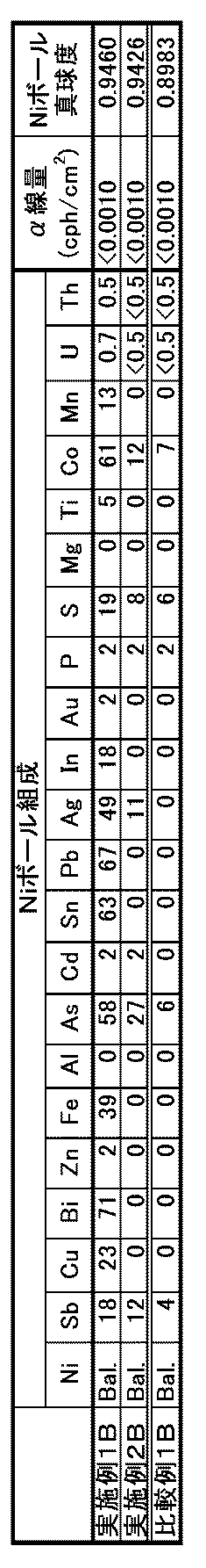
Claims (7)
- Uの含有量が5ppb以下であり、Thの含有量が5ppb以下であり、純度が99.9%以上99.995%以下であり、PbまたはBiのいずれかの含有量、あるいは、PbおよびBiの合計の含有量が1ppm以上である純金属であって、純金属に含まれる不純物の中で除去対象とした不純物の大気圧での沸点より高い大気圧での沸点を有した純金属を、
気圧により変化する沸点及び融点に応じて、除去対象とした不純物の沸点より高く、純金属の融点より高く、かつ、純金属の沸点より低い温度に設定された加熱温度で加熱して、純金属を溶融させる工程と、
溶融した純金属を球状に造球する工程を含む
ことを特徴とする金属球の製造方法。 - 純金属の大気圧での融点が900℃以上、かつ、沸点が962℃以上である
ことを特徴とする請求項1に記載の金属球の製造方法。 - 除去対象の不純物はPoである
ことを特徴とする請求項2に記載の金属球の製造方法。 - 造球された金属球を焼きなますアニーリングの工程を更に含む
ことを特徴とする請求項1~請求項3の何れか1項に記載の金属球の製造方法。 - 請求項1~請求項4の何れか1項に記載の製造方法で製造された金属球を含有することを特徴とする接合材料。
- 請求項1~請求項4の何れか1項に記載の製造方法で製造されたα線量が0.0200cph/cm2以下であり、真球度が0.90以上である
ことを特徴とする金属球。 - 請求項6に記載の金属球を含有することを特徴とする接合材料。
Priority Applications (7)
| Application Number | Priority Date | Filing Date | Title |
|---|---|---|---|
| KR1020167024128A KR20160110521A (ko) | 2014-02-04 | 2014-02-04 | 금속구의 제조 방법, 접합 재료 및 금속구 |
| PCT/JP2014/052570 WO2015118612A1 (ja) | 2014-02-04 | 2014-02-04 | 金属球の製造方法、接合材料及び金属球 |
| US15/116,275 US10150185B2 (en) | 2014-02-04 | 2014-02-04 | Method for producing metal ball, joining material, and metal ball |
| JP2014523135A JP5692467B1 (ja) | 2014-02-04 | 2014-02-04 | 金属球の製造方法、接合材料及び金属球 |
| CN201480074919.3A CN105980087B (zh) | 2014-02-04 | 2014-02-04 | 金属球的制造方法、接合材料以及金属球 |
| EP14881854.5A EP3103567A4 (en) | 2014-02-04 | 2014-02-04 | Method for producing metal ball, joining material, and metal ball |
| TW104103150A TWI638698B (zh) | 2014-02-04 | 2015-01-30 | 金屬球的製造方法、接合材料及金屬球 |
Applications Claiming Priority (1)
| Application Number | Priority Date | Filing Date | Title |
|---|---|---|---|
| PCT/JP2014/052570 WO2015118612A1 (ja) | 2014-02-04 | 2014-02-04 | 金属球の製造方法、接合材料及び金属球 |
Publications (1)
| Publication Number | Publication Date |
|---|---|
| WO2015118612A1 true WO2015118612A1 (ja) | 2015-08-13 |
Family
ID=52830789
Family Applications (1)
| Application Number | Title | Priority Date | Filing Date |
|---|---|---|---|
| PCT/JP2014/052570 WO2015118612A1 (ja) | 2014-02-04 | 2014-02-04 | 金属球の製造方法、接合材料及び金属球 |
Country Status (7)
| Country | Link |
|---|---|
| US (1) | US10150185B2 (ja) |
| EP (1) | EP3103567A4 (ja) |
| JP (1) | JP5692467B1 (ja) |
| KR (1) | KR20160110521A (ja) |
| CN (1) | CN105980087B (ja) |
| TW (1) | TWI638698B (ja) |
| WO (1) | WO2015118612A1 (ja) |
Families Citing this family (4)
| Publication number | Priority date | Publication date | Assignee | Title |
|---|---|---|---|---|
| JP6341330B1 (ja) * | 2017-12-06 | 2018-06-13 | 千住金属工業株式会社 | Cuボール、OSP処理Cuボール、Cu核ボール、はんだ継手、はんだペースト、フォームはんだ及びCuボールの製造方法 |
| JP6836091B1 (ja) * | 2020-04-10 | 2021-02-24 | 千住金属工業株式会社 | はんだ合金、はんだ粉末、ソルダペースト、はんだボール、ソルダプリフォーム及びはんだ継手 |
| JP6928295B1 (ja) * | 2020-10-02 | 2021-09-01 | 千住金属工業株式会社 | フラックス及びソルダペースト |
| JP6928296B1 (ja) * | 2020-10-02 | 2021-09-01 | 千住金属工業株式会社 | ソルダペースト |
Citations (7)
| Publication number | Priority date | Publication date | Assignee | Title |
|---|---|---|---|---|
| WO1995024113A1 (fr) * | 1994-03-01 | 1995-09-08 | Sumitomo Special Metals Company Limited | Boule en cuivre et procede de production de cette derniere |
| JPH09186161A (ja) * | 1995-12-27 | 1997-07-15 | Fujitsu Ltd | 半導体装置のはんだバンプ形成方法 |
| JP2002206103A (ja) * | 2000-11-09 | 2002-07-26 | Nikko Materials Co Ltd | 高純度ジルコニウム若しくはハフニウム粉の製造方法 |
| JP2003193283A (ja) * | 2001-12-28 | 2003-07-09 | Fujitsu Ltd | 電解めっき液及びその調製方法、半導体装置の製造方法ならびに放射性不純物の分析方法 |
| WO2007004394A1 (ja) * | 2005-07-01 | 2007-01-11 | Nippon Mining & Metals Co., Ltd. | 高純度錫又は錫合金及び高純度錫の製造方法 |
| JP2011214061A (ja) * | 2010-03-31 | 2011-10-27 | Jx Nippon Mining & Metals Corp | α線量が少ないインジウム又はインジウムを含有する合金 |
| JP2013185214A (ja) * | 2012-03-08 | 2013-09-19 | Jx Nippon Mining & Metals Corp | α線量が少ないビスマス又はビスマス合金及びその製造方法 |
Family Cites Families (11)
| Publication number | Priority date | Publication date | Assignee | Title |
|---|---|---|---|---|
| JPH084100B2 (ja) * | 1987-02-27 | 1996-01-17 | タツタ電線株式会社 | ボンディング線 |
| KR100572262B1 (ko) * | 2000-10-02 | 2006-04-19 | 가부시키 가이샤 닛코 마테리알즈 | 고순도 지르코늄 또는 하프늄의 제조방법 |
| JP3891346B2 (ja) * | 2002-01-07 | 2007-03-14 | 千住金属工業株式会社 | 微小銅ボールおよび微小銅ボールの製造方法 |
| JP2005036301A (ja) * | 2003-06-23 | 2005-02-10 | Allied Material Corp | 微小金属球及びその製造方法 |
| US20060186179A1 (en) * | 2005-02-23 | 2006-08-24 | Levine Lee R | Apparatus and method for bonding wires |
| JP2007287712A (ja) | 2006-04-12 | 2007-11-01 | Oki Electric Ind Co Ltd | 半導体装置、半導体装置の実装構造、及びそれらの製造方法 |
| KR101623629B1 (ko) * | 2011-03-07 | 2016-05-23 | 제이엑스 킨조쿠 가부시키가이샤 | 구리 또는 구리 합금, 본딩 와이어, 구리의 제조 방법, 구리 합금의 제조 방법 및 본딩 와이어의 제조 방법 |
| US9668358B2 (en) | 2012-12-06 | 2017-05-30 | Senju Metal Industry Co., Ltd. | Cu ball |
| CN105392580B (zh) * | 2013-06-19 | 2017-04-26 | 千住金属工业株式会社 | Cu芯球 |
| CN105745043B (zh) | 2013-09-19 | 2017-11-24 | 千住金属工业株式会社 | Ni球、Ni芯球、钎焊接头、成形焊料、焊膏 |
| KR101858884B1 (ko) | 2013-11-05 | 2018-05-16 | 센주긴조쿠고교 가부시키가이샤 | Cu 핵 볼, 땜납 페이스트, 폼 땜납 및 납땜 조인트 |
-
2014
- 2014-02-04 KR KR1020167024128A patent/KR20160110521A/ko not_active Application Discontinuation
- 2014-02-04 WO PCT/JP2014/052570 patent/WO2015118612A1/ja active Application Filing
- 2014-02-04 CN CN201480074919.3A patent/CN105980087B/zh active Active
- 2014-02-04 JP JP2014523135A patent/JP5692467B1/ja active Active
- 2014-02-04 EP EP14881854.5A patent/EP3103567A4/en not_active Withdrawn
- 2014-02-04 US US15/116,275 patent/US10150185B2/en active Active
-
2015
- 2015-01-30 TW TW104103150A patent/TWI638698B/zh active
Patent Citations (7)
| Publication number | Priority date | Publication date | Assignee | Title |
|---|---|---|---|---|
| WO1995024113A1 (fr) * | 1994-03-01 | 1995-09-08 | Sumitomo Special Metals Company Limited | Boule en cuivre et procede de production de cette derniere |
| JPH09186161A (ja) * | 1995-12-27 | 1997-07-15 | Fujitsu Ltd | 半導体装置のはんだバンプ形成方法 |
| JP2002206103A (ja) * | 2000-11-09 | 2002-07-26 | Nikko Materials Co Ltd | 高純度ジルコニウム若しくはハフニウム粉の製造方法 |
| JP2003193283A (ja) * | 2001-12-28 | 2003-07-09 | Fujitsu Ltd | 電解めっき液及びその調製方法、半導体装置の製造方法ならびに放射性不純物の分析方法 |
| WO2007004394A1 (ja) * | 2005-07-01 | 2007-01-11 | Nippon Mining & Metals Co., Ltd. | 高純度錫又は錫合金及び高純度錫の製造方法 |
| JP2011214061A (ja) * | 2010-03-31 | 2011-10-27 | Jx Nippon Mining & Metals Corp | α線量が少ないインジウム又はインジウムを含有する合金 |
| JP2013185214A (ja) * | 2012-03-08 | 2013-09-19 | Jx Nippon Mining & Metals Corp | α線量が少ないビスマス又はビスマス合金及びその製造方法 |
Non-Patent Citations (1)
| Title |
|---|
| See also references of EP3103567A4 * |
Also Published As
| Publication number | Publication date |
|---|---|
| TW201544225A (zh) | 2015-12-01 |
| CN105980087B (zh) | 2018-05-25 |
| CN105980087A (zh) | 2016-09-28 |
| US20170182600A1 (en) | 2017-06-29 |
| US10150185B2 (en) | 2018-12-11 |
| EP3103567A4 (en) | 2017-11-01 |
| JPWO2015118612A1 (ja) | 2017-03-23 |
| JP5692467B1 (ja) | 2015-04-01 |
| TWI638698B (zh) | 2018-10-21 |
| EP3103567A1 (en) | 2016-12-14 |
| KR20160110521A (ko) | 2016-09-21 |
Similar Documents
| Publication | Publication Date | Title |
|---|---|---|
| JP5585751B1 (ja) | Cuボール、Cu核ボール、はんだ継手、はんだペースト、およびフォームはんだ | |
| JP5435182B1 (ja) | Cuボール | |
| JP5534122B1 (ja) | 核ボール、はんだペースト、フォームはんだ、フラックスコート核ボールおよびはんだ継手 | |
| JP5408401B1 (ja) | Cu核ボール | |
| JP5652560B1 (ja) | Cu核ボール、はんだペースト、フォームはんだ及びはんだ継手 | |
| JP5692467B1 (ja) | 金属球の製造方法、接合材料及び金属球 | |
| WO2015040714A1 (ja) | Niボール、Ni核ボール、はんだ継手、フォームはんだ、はんだペースト | |
| TWI753220B (zh) | Cu球、OSP處理Cu球、Cu核球、焊接接頭、焊膏、泡沫焊料及Cu球的製造方法 | |
| JP5585752B1 (ja) | Niボール、Ni核ボール、はんだ継手、はんだペースト、およびフォームはんだ |
Legal Events
| Date | Code | Title | Description |
|---|---|---|---|
| ENP | Entry into the national phase |
Ref document number: 2014523135 Country of ref document: JP Kind code of ref document: A |
|
| 121 | Ep: the epo has been informed by wipo that ep was designated in this application |
Ref document number: 14881854 Country of ref document: EP Kind code of ref document: A1 |
|
| NENP | Non-entry into the national phase |
Ref country code: DE |
|
| REEP | Request for entry into the european phase |
Ref document number: 2014881854 Country of ref document: EP |
|
| WWE | Wipo information: entry into national phase |
Ref document number: 2014881854 Country of ref document: EP |
|
| ENP | Entry into the national phase |
Ref document number: 20167024128 Country of ref document: KR Kind code of ref document: A |
|
| WWE | Wipo information: entry into national phase |
Ref document number: 15116275 Country of ref document: US |