WO2015111211A1 - パワーモジュール及びその製造方法 - Google Patents
パワーモジュール及びその製造方法 Download PDFInfo
- Publication number
- WO2015111211A1 WO2015111211A1 PCT/JP2014/051643 JP2014051643W WO2015111211A1 WO 2015111211 A1 WO2015111211 A1 WO 2015111211A1 JP 2014051643 W JP2014051643 W JP 2014051643W WO 2015111211 A1 WO2015111211 A1 WO 2015111211A1
- Authority
- WO
- WIPO (PCT)
- Prior art keywords
- cooling
- main body
- power module
- metal member
- bus bar
- Prior art date
Links
Images


Classifications
-
- H—ELECTRICITY
- H05—ELECTRIC TECHNIQUES NOT OTHERWISE PROVIDED FOR
- H05K—PRINTED CIRCUITS; CASINGS OR CONSTRUCTIONAL DETAILS OF ELECTRIC APPARATUS; MANUFACTURE OF ASSEMBLAGES OF ELECTRICAL COMPONENTS
- H05K7/00—Constructional details common to different types of electric apparatus
- H05K7/20—Modifications to facilitate cooling, ventilating, or heating
- H05K7/2089—Modifications to facilitate cooling, ventilating, or heating for power electronics, e.g. for inverters for controlling motor
- H05K7/20927—Liquid coolant without phase change
-
- H—ELECTRICITY
- H01—ELECTRIC ELEMENTS
- H01L—SEMICONDUCTOR DEVICES NOT COVERED BY CLASS H10
- H01L21/00—Processes or apparatus adapted for the manufacture or treatment of semiconductor or solid state devices or of parts thereof
- H01L21/02—Manufacture or treatment of semiconductor devices or of parts thereof
- H01L21/04—Manufacture or treatment of semiconductor devices or of parts thereof the devices having at least one potential-jump barrier or surface barrier, e.g. PN junction, depletion layer or carrier concentration layer
- H01L21/48—Manufacture or treatment of parts, e.g. containers, prior to assembly of the devices, using processes not provided for in a single one of the subgroups H01L21/06 - H01L21/326
- H01L21/4814—Conductive parts
- H01L21/4817—Conductive parts for containers, e.g. caps
-
- H—ELECTRICITY
- H01—ELECTRIC ELEMENTS
- H01L—SEMICONDUCTOR DEVICES NOT COVERED BY CLASS H10
- H01L21/00—Processes or apparatus adapted for the manufacture or treatment of semiconductor or solid state devices or of parts thereof
- H01L21/02—Manufacture or treatment of semiconductor devices or of parts thereof
- H01L21/04—Manufacture or treatment of semiconductor devices or of parts thereof the devices having at least one potential-jump barrier or surface barrier, e.g. PN junction, depletion layer or carrier concentration layer
- H01L21/48—Manufacture or treatment of parts, e.g. containers, prior to assembly of the devices, using processes not provided for in a single one of the subgroups H01L21/06 - H01L21/326
- H01L21/4814—Conductive parts
- H01L21/4846—Leads on or in insulating or insulated substrates, e.g. metallisation
- H01L21/4857—Multilayer substrates
-
- H—ELECTRICITY
- H01—ELECTRIC ELEMENTS
- H01L—SEMICONDUCTOR DEVICES NOT COVERED BY CLASS H10
- H01L21/00—Processes or apparatus adapted for the manufacture or treatment of semiconductor or solid state devices or of parts thereof
- H01L21/02—Manufacture or treatment of semiconductor devices or of parts thereof
- H01L21/04—Manufacture or treatment of semiconductor devices or of parts thereof the devices having at least one potential-jump barrier or surface barrier, e.g. PN junction, depletion layer or carrier concentration layer
- H01L21/50—Assembly of semiconductor devices using processes or apparatus not provided for in a single one of the subgroups H01L21/06 - H01L21/326, e.g. sealing of a cap to a base of a container
- H01L21/54—Providing fillings in containers, e.g. gas fillings
-
- H—ELECTRICITY
- H01—ELECTRIC ELEMENTS
- H01L—SEMICONDUCTOR DEVICES NOT COVERED BY CLASS H10
- H01L23/00—Details of semiconductor or other solid state devices
- H01L23/02—Containers; Seals
- H01L23/04—Containers; Seals characterised by the shape of the container or parts, e.g. caps, walls
- H01L23/043—Containers; Seals characterised by the shape of the container or parts, e.g. caps, walls the container being a hollow construction and having a conductive base as a mounting as well as a lead for the semiconductor body
-
- H—ELECTRICITY
- H01—ELECTRIC ELEMENTS
- H01L—SEMICONDUCTOR DEVICES NOT COVERED BY CLASS H10
- H01L23/00—Details of semiconductor or other solid state devices
- H01L23/16—Fillings or auxiliary members in containers or encapsulations, e.g. centering rings
- H01L23/18—Fillings characterised by the material, its physical or chemical properties, or its arrangement within the complete device
- H01L23/24—Fillings characterised by the material, its physical or chemical properties, or its arrangement within the complete device solid or gel at the normal operating temperature of the device
-
- H—ELECTRICITY
- H01—ELECTRIC ELEMENTS
- H01L—SEMICONDUCTOR DEVICES NOT COVERED BY CLASS H10
- H01L23/00—Details of semiconductor or other solid state devices
- H01L23/34—Arrangements for cooling, heating, ventilating or temperature compensation ; Temperature sensing arrangements
- H01L23/36—Selection of materials, or shaping, to facilitate cooling or heating, e.g. heatsinks
- H01L23/367—Cooling facilitated by shape of device
- H01L23/3675—Cooling facilitated by shape of device characterised by the shape of the housing
-
- H—ELECTRICITY
- H01—ELECTRIC ELEMENTS
- H01L—SEMICONDUCTOR DEVICES NOT COVERED BY CLASS H10
- H01L23/00—Details of semiconductor or other solid state devices
- H01L23/34—Arrangements for cooling, heating, ventilating or temperature compensation ; Temperature sensing arrangements
- H01L23/36—Selection of materials, or shaping, to facilitate cooling or heating, e.g. heatsinks
- H01L23/373—Cooling facilitated by selection of materials for the device or materials for thermal expansion adaptation, e.g. carbon
- H01L23/3735—Laminates or multilayers, e.g. direct bond copper ceramic substrates
-
- H—ELECTRICITY
- H01—ELECTRIC ELEMENTS
- H01L—SEMICONDUCTOR DEVICES NOT COVERED BY CLASS H10
- H01L23/00—Details of semiconductor or other solid state devices
- H01L23/34—Arrangements for cooling, heating, ventilating or temperature compensation ; Temperature sensing arrangements
- H01L23/40—Mountings or securing means for detachable cooling or heating arrangements ; fixed by friction, plugs or springs
- H01L23/4006—Mountings or securing means for detachable cooling or heating arrangements ; fixed by friction, plugs or springs with bolts or screws
-
- H—ELECTRICITY
- H01—ELECTRIC ELEMENTS
- H01L—SEMICONDUCTOR DEVICES NOT COVERED BY CLASS H10
- H01L23/00—Details of semiconductor or other solid state devices
- H01L23/34—Arrangements for cooling, heating, ventilating or temperature compensation ; Temperature sensing arrangements
- H01L23/46—Arrangements for cooling, heating, ventilating or temperature compensation ; Temperature sensing arrangements involving the transfer of heat by flowing fluids
- H01L23/473—Arrangements for cooling, heating, ventilating or temperature compensation ; Temperature sensing arrangements involving the transfer of heat by flowing fluids by flowing liquids
-
- H—ELECTRICITY
- H01—ELECTRIC ELEMENTS
- H01L—SEMICONDUCTOR DEVICES NOT COVERED BY CLASS H10
- H01L23/00—Details of semiconductor or other solid state devices
- H01L23/48—Arrangements for conducting electric current to or from the solid state body in operation, e.g. leads, terminal arrangements ; Selection of materials therefor
- H01L23/488—Arrangements for conducting electric current to or from the solid state body in operation, e.g. leads, terminal arrangements ; Selection of materials therefor consisting of soldered or bonded constructions
- H01L23/498—Leads, i.e. metallisations or lead-frames on insulating substrates, e.g. chip carriers
- H01L23/49822—Multilayer substrates
-
- H—ELECTRICITY
- H01—ELECTRIC ELEMENTS
- H01L—SEMICONDUCTOR DEVICES NOT COVERED BY CLASS H10
- H01L23/00—Details of semiconductor or other solid state devices
- H01L23/48—Arrangements for conducting electric current to or from the solid state body in operation, e.g. leads, terminal arrangements ; Selection of materials therefor
- H01L23/488—Arrangements for conducting electric current to or from the solid state body in operation, e.g. leads, terminal arrangements ; Selection of materials therefor consisting of soldered or bonded constructions
- H01L23/498—Leads, i.e. metallisations or lead-frames on insulating substrates, e.g. chip carriers
- H01L23/49838—Geometry or layout
-
- H—ELECTRICITY
- H01—ELECTRIC ELEMENTS
- H01L—SEMICONDUCTOR DEVICES NOT COVERED BY CLASS H10
- H01L24/00—Arrangements for connecting or disconnecting semiconductor or solid-state bodies; Methods or apparatus related thereto
- H01L24/01—Means for bonding being attached to, or being formed on, the surface to be connected, e.g. chip-to-package, die-attach, "first-level" interconnects; Manufacturing methods related thereto
- H01L24/26—Layer connectors, e.g. plate connectors, solder or adhesive layers; Manufacturing methods related thereto
- H01L24/31—Structure, shape, material or disposition of the layer connectors after the connecting process
- H01L24/33—Structure, shape, material or disposition of the layer connectors after the connecting process of a plurality of layer connectors
-
- H—ELECTRICITY
- H01—ELECTRIC ELEMENTS
- H01L—SEMICONDUCTOR DEVICES NOT COVERED BY CLASS H10
- H01L25/00—Assemblies consisting of a plurality of individual semiconductor or other solid state devices ; Multistep manufacturing processes thereof
- H01L25/03—Assemblies consisting of a plurality of individual semiconductor or other solid state devices ; Multistep manufacturing processes thereof all the devices being of a type provided for in the same subgroup of groups H01L27/00 - H01L33/00, or in a single subclass of H10K, H10N, e.g. assemblies of rectifier diodes
- H01L25/04—Assemblies consisting of a plurality of individual semiconductor or other solid state devices ; Multistep manufacturing processes thereof all the devices being of a type provided for in the same subgroup of groups H01L27/00 - H01L33/00, or in a single subclass of H10K, H10N, e.g. assemblies of rectifier diodes the devices not having separate containers
- H01L25/07—Assemblies consisting of a plurality of individual semiconductor or other solid state devices ; Multistep manufacturing processes thereof all the devices being of a type provided for in the same subgroup of groups H01L27/00 - H01L33/00, or in a single subclass of H10K, H10N, e.g. assemblies of rectifier diodes the devices not having separate containers the devices being of a type provided for in group H01L29/00
- H01L25/072—Assemblies consisting of a plurality of individual semiconductor or other solid state devices ; Multistep manufacturing processes thereof all the devices being of a type provided for in the same subgroup of groups H01L27/00 - H01L33/00, or in a single subclass of H10K, H10N, e.g. assemblies of rectifier diodes the devices not having separate containers the devices being of a type provided for in group H01L29/00 the devices being arranged next to each other
-
- H—ELECTRICITY
- H01—ELECTRIC ELEMENTS
- H01L—SEMICONDUCTOR DEVICES NOT COVERED BY CLASS H10
- H01L25/00—Assemblies consisting of a plurality of individual semiconductor or other solid state devices ; Multistep manufacturing processes thereof
- H01L25/18—Assemblies consisting of a plurality of individual semiconductor or other solid state devices ; Multistep manufacturing processes thereof the devices being of types provided for in two or more different subgroups of the same main group of groups H01L27/00 - H01L33/00, or in a single subclass of H10K, H10N
-
- H—ELECTRICITY
- H01—ELECTRIC ELEMENTS
- H01L—SEMICONDUCTOR DEVICES NOT COVERED BY CLASS H10
- H01L2224/00—Indexing scheme for arrangements for connecting or disconnecting semiconductor or solid-state bodies and methods related thereto as covered by H01L24/00
- H01L2224/01—Means for bonding being attached to, or being formed on, the surface to be connected, e.g. chip-to-package, die-attach, "first-level" interconnects; Manufacturing methods related thereto
- H01L2224/26—Layer connectors, e.g. plate connectors, solder or adhesive layers; Manufacturing methods related thereto
- H01L2224/2612—Auxiliary members for layer connectors, e.g. spacers
-
- H—ELECTRICITY
- H01—ELECTRIC ELEMENTS
- H01L—SEMICONDUCTOR DEVICES NOT COVERED BY CLASS H10
- H01L23/00—Details of semiconductor or other solid state devices
- H01L23/02—Containers; Seals
- H01L23/04—Containers; Seals characterised by the shape of the container or parts, e.g. caps, walls
- H01L23/043—Containers; Seals characterised by the shape of the container or parts, e.g. caps, walls the container being a hollow construction and having a conductive base as a mounting as well as a lead for the semiconductor body
- H01L23/051—Containers; Seals characterised by the shape of the container or parts, e.g. caps, walls the container being a hollow construction and having a conductive base as a mounting as well as a lead for the semiconductor body another lead being formed by a cover plate parallel to the base plate, e.g. sandwich type
-
- H—ELECTRICITY
- H01—ELECTRIC ELEMENTS
- H01L—SEMICONDUCTOR DEVICES NOT COVERED BY CLASS H10
- H01L23/00—Details of semiconductor or other solid state devices
- H01L23/28—Encapsulations, e.g. encapsulating layers, coatings, e.g. for protection
- H01L23/31—Encapsulations, e.g. encapsulating layers, coatings, e.g. for protection characterised by the arrangement or shape
- H01L23/3107—Encapsulations, e.g. encapsulating layers, coatings, e.g. for protection characterised by the arrangement or shape the device being completely enclosed
-
- H—ELECTRICITY
- H01—ELECTRIC ELEMENTS
- H01L—SEMICONDUCTOR DEVICES NOT COVERED BY CLASS H10
- H01L23/00—Details of semiconductor or other solid state devices
- H01L23/34—Arrangements for cooling, heating, ventilating or temperature compensation ; Temperature sensing arrangements
- H01L23/40—Mountings or securing means for detachable cooling or heating arrangements ; fixed by friction, plugs or springs
- H01L23/4006—Mountings or securing means for detachable cooling or heating arrangements ; fixed by friction, plugs or springs with bolts or screws
- H01L23/4012—Mountings or securing means for detachable cooling or heating arrangements ; fixed by friction, plugs or springs with bolts or screws for stacked arrangements of a plurality of semiconductor devices
-
- H—ELECTRICITY
- H01—ELECTRIC ELEMENTS
- H01L—SEMICONDUCTOR DEVICES NOT COVERED BY CLASS H10
- H01L23/00—Details of semiconductor or other solid state devices
- H01L23/34—Arrangements for cooling, heating, ventilating or temperature compensation ; Temperature sensing arrangements
- H01L23/42—Fillings or auxiliary members in containers or encapsulations selected or arranged to facilitate heating or cooling
- H01L23/433—Auxiliary members in containers characterised by their shape, e.g. pistons
- H01L23/4334—Auxiliary members in encapsulations
-
- H—ELECTRICITY
- H01—ELECTRIC ELEMENTS
- H01L—SEMICONDUCTOR DEVICES NOT COVERED BY CLASS H10
- H01L2924/00—Indexing scheme for arrangements or methods for connecting or disconnecting semiconductor or solid-state bodies as covered by H01L24/00
- H01L2924/10—Details of semiconductor or other solid state devices to be connected
- H01L2924/11—Device type
- H01L2924/13—Discrete devices, e.g. 3 terminal devices
- H01L2924/1304—Transistor
- H01L2924/1305—Bipolar Junction Transistor [BJT]
- H01L2924/13055—Insulated gate bipolar transistor [IGBT]
-
- H—ELECTRICITY
- H01—ELECTRIC ELEMENTS
- H01L—SEMICONDUCTOR DEVICES NOT COVERED BY CLASS H10
- H01L2924/00—Indexing scheme for arrangements or methods for connecting or disconnecting semiconductor or solid-state bodies as covered by H01L24/00
- H01L2924/10—Details of semiconductor or other solid state devices to be connected
- H01L2924/11—Device type
- H01L2924/13—Discrete devices, e.g. 3 terminal devices
- H01L2924/1304—Transistor
- H01L2924/1306—Field-effect transistor [FET]
- H01L2924/13091—Metal-Oxide-Semiconductor Field-Effect Transistor [MOSFET]
Definitions
- the present invention relates to a power module including a semiconductor element and a manufacturing method thereof.
- a power conversion device including a semiconductor element called a power semiconductor chip has been used in automobiles, railways, power equipment, and the like.
- a high-efficiency power semiconductor chip in a power conversion device, energy loss during power conversion can be reduced.
- the power semiconductor chip since the power semiconductor chip generates a large amount of heat when energized, it is required to cool the power semiconductor chip and keep it at an appropriate temperature. There is also a demand for miniaturization of power semiconductor chips.
- Patent Document 1 describes a power conversion device including a semiconductor module incorporating a switching element and a cooling tube for cooling the semiconductor module.
- a pair of spring members are installed at both ends of a laminated body in which semiconductor modules and cooling tubes are alternately laminated.
- Patent Document 2 discloses a power semiconductor device including a plurality of pairs of power modules arranged so that mold surfaces come into contact with each other and cooling fins that sandwich the heat radiation surfaces of the pair of power modules from both sides. Are listed.
- the power conversion device described in Patent Document 1 has a configuration in which a laminated body is fixed to a storage case having an H-shaped cross-sectional view, a control terminal is exposed from one side of the storage case, and a power terminal is exposed from the other side. It has become.
- an object of the present invention is to provide a power module and the like that achieve low inductance and downsizing. Moreover, this invention makes it a subject to provide the power module etc. which improved the workability
- a power module includes a semiconductor element, a control terminal connected to the semiconductor element, a power terminal through which a current corresponding to an electric signal to the control terminal flows, and a heat dissipation layer. And a main body part, a cooling part that is arranged so as to be able to exchange heat with the heat radiating layer, cool the main body part, a bus bar connected to the power terminal, and at least a contact point between the bus bar is insulative.
- a cylindrical body, and a metal member that supports the cylindrical body, and the cylindrical body is in close contact with the metallic member to form a box body that is open on one side.
- the main body portion and the bus bar are disposed, the control terminal and the power terminal extend from the semiconductor element to the one side, and an insulating sealing material is filled in the box, thereby the main body. Part Wherein the bus bar is sealed.
- a power module or the like with a reduced inductance and a reduced size.
- a power module or the like with improved workability during manufacturing can be provided.
- FIG. 3 is an end view taken along the line CC shown in FIG. 2. It is the disassembled perspective view which looked down at the power module from the right rear.
- FIG. 2 is an end view taken along line AA shown in FIG.
- FIG. 3 is an end view taken along line BB shown in FIG. 1.
- It is a perspective view for demonstrating the manufacturing process of a power module. It is a disassembled perspective view which shows the modification 1 of the power module which concerns on 1st Embodiment of this invention.
- FIG. 2 is an end view of the power module (corresponding to line AA shown in FIG. 1). It is a disassembled perspective view which shows the modification 1 of the power module which concerns on 2nd Embodiment of this invention. It is a disassembled perspective view which shows the modification 2 of the power module which concerns on 2nd Embodiment of this invention. It is a disassembled perspective view which shows the modification 3 of the power module which concerns on 2nd Embodiment of this invention.
- FIG. 2 is an end view of the power module (corresponding to line AA shown in FIG. 1).
- FIG. 9 is an end view (corresponding to the line AA shown in FIG. 1) of a power module according to a fourth embodiment of the present invention.
- FIG. 9 is an end view (corresponding to the line AA shown in FIG. 1) of a power module according to a fifth embodiment of the present invention.
- It is the perspective view which looked down at the power module concerning a 6th embodiment of the present invention from the right rear.
- FIG. 20 is an end view taken along line AA shown in FIG. FIG.
- FIG. 20 is an end view (corresponding to the line AA shown in FIG. 19) showing a first modification of the power module according to the sixth embodiment of the present invention.
- FIG. 29 is an end view (corresponding to the AA line shown in FIG. 19) showing a second modification of the power module according to the sixth embodiment of the present invention. It is the disassembled perspective view which looked down at the power module which concerns on 7th Embodiment of this invention from the right rear.
- FIG. 20 is an end view of the power module (corresponding to line AA shown in FIG. 19).
- FIG. 29 is an end view (corresponding to the line AA shown in FIG. 19) showing a first modification of the power module according to the seventh embodiment of the present invention.
- FIG. 29 is an end view (corresponding to the line AA shown in FIG.
- FIG. 20 is an end view (corresponding to line AA shown in FIG. 19) of a power module according to an eighth embodiment of the present invention. It is an end view of the power module which concerns on a comparative example.
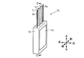
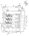
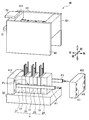
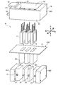
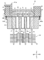
- FIG. 1 is a perspective view of the power module according to this embodiment as viewed from the right rear.
- the power module M is used, for example, in a high-voltage power converter (not shown), and performs a switching operation in response to a command from an external control device (not shown).
- the power module M includes three main body portions 11 to 13 (see FIG. 4), four cooling portions 21 to 24, a metal member 30, and a cylindrical body W (left wall 41, right wall 42, front wall 43, rear Wall 44), collector connection bus bar 51, and emitter connection bus bar 52.
- FIG. 2 is a perspective view of the main body.
- the main body 11 conducts / cuts off the collector terminal 1i and the emitter terminal 1j in accordance with an electric signal input via the control terminal 1b.
- the main-body part 11 is exhibiting rectangular parallelepiped shape, However, The shape of the main-body part 11 is not limited to this.
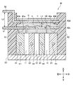
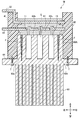
- FIG. 3 is an end view taken along line CC shown in FIG.
- the main body 11 mainly includes a power semiconductor element 1a, a control terminal 1b (see FIG. 2), wiring layers 1c and 1f, insulating layers 1d and 1g, heat radiation layers 1e and 1h, a collector terminal 1i, And an emitter terminal 1j (see FIG. 2).
- the power semiconductor element 1 a semiconductor element
- the power semiconductor element 1 a is, for example, an IGBT (Insulated Gate Bipolar Transistor) and is built in the main body 11.
- the type of the power semiconductor element 1a is not limited to this, and various elements such as a MOSFET (Metal-Oxide-Semiconductor Field Effect Transistor), a GTO (Gate Turn-Off thyristor), and a diode can be used.
- MOSFET Metal-Oxide-Semiconductor Field Effect Transistor
- GTO Gate Turn-Off thyristor
- the control terminal 1b shown in FIG. 2 is a terminal for inputting an electric signal input from an external control device (not shown) to the power semiconductor element 1a.
- the control terminal 1b is connected to the gate electrode of the power semiconductor element 1a and extends upward from the power semiconductor element 1a (see FIG. 2).
- a collector-side wiring layer 1 c, an insulating layer 1 d, and a heat dissipation layer 1 e are stacked in order from the power semiconductor element 1 a toward the left side surface of the main body 11.
- an emitter-side wiring layer 1 f, an insulating layer 1 g, and a heat dissipation layer 1 h are stacked in order from the power semiconductor element 1 a toward the right side surface of the main body 11.
- the collector-side wiring layer 1c, the insulating layer 1d, and the heat dissipation layer 1e will be mainly described, but the same applies to the emitter side.
- the wiring layer 1c contains a metal having a low electric resistance, such as copper (Cu), aluminum (Al), an alloy of copper and aluminum.
- a layer (not shown) having high thermal conductivity and low thermal expansion between the wiring layer 1c and the insulating layer 1d.
- the above-described layer is formed by diffusing molybdenum, tungsten, carbon, or the like on one side (insulating layer 1d side) of the wiring layer 1c. As a result, it is possible to maintain current withstand capability and heat spreadability while relaxing thermal stress applied to the power semiconductor element 1a.
- the wiring layer 1 c has a thin plate shape, and the surface direction thereof is parallel to the left and right side surfaces of the main body 11. Further, the collector-side wiring layer 1c and the emitter-side wiring layer 1f are arranged so that currents in opposite directions flow. By arranging the wiring layers 1c and 1f in this way, the magnetic fields of the wiring layers 1c and 1f are canceled out and the inductance can be reduced.
- the power semiconductor element 1a and the wiring layer 1c are electrically bonded using, for example, a bonding material mainly composed of silver oxide (AgO, Ag 2 O) or copper oxide (CuO) particles having a particle size of 50 ⁇ m or less.
- the collector terminal 1i (power terminal) and the emitter terminal 1j (power terminal: see FIG. 2) are terminals for passing a current according to the voltage between the control terminals 1b.
- the collector terminal 1i is connected to the collector-side wiring layer 1c (see FIG. 3), and the emitter terminal 1j is connected to the emitter-side wiring layer 1f.
- the collector terminal 1i and the emitter terminal 1j extend upward from the power semiconductor element 1a.
- the insulating layer 1d shown in FIG. 3 is a resin in which a high thermal conductive filler such as alumina, aluminum nitride, or boron nitride is dispersed in a sintered plate made of a high thermal conductive material such as alumina, aluminum nitride, or silicon nitride.
- the heat dissipating layer 1e is provided to release heat generated in the power semiconductor element 1a and the like to the outside, and includes a highly thermally conductive metal made of copper, aluminum, or copper and an aluminum alloy.
- molybdenum, tungsten, and carbon are diffused in the above-described metal to achieve high thermal conductivity and low thermal expansion.
- the heat dissipation layers 1e and 1h are exposed from the left and right side surfaces of the power semiconductor element 1a.
- the exposed surfaces of the heat radiation layers 1e and 1h are preferably flat and parallel to each other. Thereby, the pressure which acts on the thermal radiation layers 1e and 1h from the cooling parts 21 and 22 (refer FIG. 4) is equalized on the above-mentioned exposed surface, and the cooling efficiency of the main-body part 11 can be improved.
- the resin member 1k is a member that seals each layer including the power semiconductor element 1a by transfer molding.
- the control terminal 1b, the collector terminal 1i, and the emitter terminal 1j are positioned in the arrangement shown in FIGS.
- an adhesive resin such as phenol, acrylic, polyimide, polyamideimide, epoxy, silicon, bismaleimide triazine, and cyanate ester can be used.
- SiO 2, Al 2 O 3 , AlN, and ceramic such as BN, gels, be rubber contained in the resin member 1k preferred.
- the resin member 1k has a low thermal expansion, and the thermal stress acting on the power semiconductor element 1a and the insulating layers 1d and 1g can be reduced.
- the heat radiation layers 1e and 1h are exposed from the resin member 1k.
- the heat radiation layers 1e and 1h are not exposed, for example, it is preferable to expose the heat radiation layers 1e and 1h by grinding a resin member that hides the heat radiation layers 1e and 1h.
- FIG. 3 by providing the heat radiation layer 1e (1h) outside the insulating layer 1d (1g) and further sealing with the resin member 1k, the insulation and heat conductivity of the main body 11 can be sufficiently secured. .
- the configuration illustrated in FIG. 3 is an example, and the configuration of the main body 11 is not limited to this.
- the other main body parts 12 and 13 also have the same configuration.
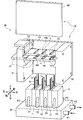
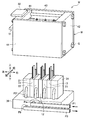
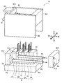
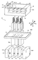
- FIG. 4 is an exploded perspective view of the power module as viewed from the right rear.
- the cooling part 21 is for cooling the main body part 11 and the like, and is arranged so as to be able to exchange heat with the heat dissipation layer 1e.
- the cooling part 21 is a metal member (for example, copper) with high heat conductivity, and its outer shape has a rectangular parallelepiped shape. The same applies to the other cooling units 22 to 24.
- the main body portions 11 to 13 are collectively referred to as “main body portion 10”
- the cooling portions 21 to 24 are collectively referred to as “cooling portion 20”.
- the power module M includes four cooling units 21 to 24. As shown in FIG. 4, the main body 10 and the cooling unit 20 are alternately arranged (laminated) in the left-right direction. In addition, the laminated body K which consists of the main-body part 10 and the cooling part 20 is pressed in the left-right direction with the fastener Q (refer FIG. 7) mentioned later. As a result, the heat dissipation layers 1e and 1h of the main body 10 and the cooling unit 20 are in close contact with each other, and heat generated in the power semiconductor element 1a and the like is radiated to the cooling unit 20 through the heat dissipation layers 1e and 1h.
- the cooling unit 20 is provided with a flow path H1 (see FIG. 5) through which cold water flows.
- a cooling pipe P2 is connected to each of the upstream end and the downstream end of the flow path H1 (see FIG. 4).
- a high heat conductive sheet such as grease or carbon sheet between the main body 10 and the cooling unit 20.
- a high heat conductive sheet such as grease or carbon sheet
- a metal member 30 shown in FIG. 4 supports a cylindrical body W which will be described later, and has a thin rectangular parallelepiped shape in the vertical direction.
- the metal member 30 has a function of releasing the heat absorbed by the cooling unit 20 to the outside, and a function of preventing the insulating sealing material G from leaking by being in close contact with the cylindrical body W.
- the metal member 30 is preferably formed of a metal that can be easily formed, such as copper (Cu), aluminum (Al), or an alloy of copper and aluminum.
- the stacked body K including the main body 10 and the cooling unit 20 is placed.
- a flow path (not shown) for allowing cooling water to flow therethrough is formed inside the metal member 30.
- the metal member 30 is provided with the cooling water inflow port and the outflow port on the right side surface, and the upper surface is provided with the connection ports (eight pieces) of the cooling pipe P2 (see FIG. 4).
- the flow path formed inside the metal member 30 divides the cooling water flowing in from the inflow port corresponding to each cooling unit 21 to 24, and merges the cooling water absorbed by the cooling units 21 to 24. It is formed so as to be taken out from the outlet.
- the cylindrical body W (the left wall 41, the right wall 42, the front wall 43, and the rear wall 44) has a rectangular hole H2 (see FIG. 1) in a plan view, and is in close contact with the metal member 30 described above. Yes.
- a box B (see FIG. 1) with one side (upper side) opened is formed.
- the left wall 41 and the right wall 42 are insulating members that fix and support the collector connection bus bar 51 and the emitter connection bus bar 52, and have a thin rectangular parallelepiped shape in the left-right direction. That is, at least the portions (the left wall 41 and the right wall 42) that are in contact with the bus bars 51 and 52 in the cylindrical body W described above have insulating properties.
- the left wall 41 and the right wall 42 are made of, for example, polyphenylene sulfide resin (Poly Phenylene Sulfide Resin).
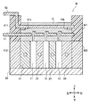
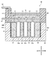
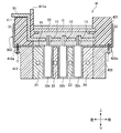
- FIG. 5 is an end view taken along line AA shown in FIG.
- the left wall 41 has a protrusion 41 a that supports the collector connection bus bar 51 and a protrusion 41 b that supports the emitter connection bus bar 52.
- Each protrusion 41a, 41b protrudes to the right and extends in the front-rear direction.
- the protrusions 41a and 41b are formed so as to ensure an insulation distance between the bus bars 51 and 52 in a state where the protrusions 41a and 41b are sealed with an insulating sealing material G described later.
- the position (height) at which the lower protrusion 41a is provided corresponds to the length of the cooling part 21 in the vertical direction, and the cooling part 21 is fitted into a recess formed by the metal member 30 and the protrusion 41a. Similarly, the cooling unit 24 is fitted into a recess formed by the metal member 30 and the protrusion 42a.
- the laminated body K which consists of the main-body part 10 and the cooling part 20 can be positioned easily and with high precision.
- the recessed parts 42c and 42d by which the right end of each bus-bar 51 and 52 is fitted are formed above the projection parts 42a and 42b provided in the right wall 42. As shown in FIG.
- the front wall 43 and the rear wall 44 are also preferably insulating members (for example, polyphenylene sulfide resin).
- the collector connection bus bar 51 (bus bar) shown in FIG. 4 is a metal member that is electrically connected to the collector terminal 1i.
- the collector connection bus bar 51 has a thin plate shape in order to reduce electrical resistance and reduce Joule heat accompanying a large current.
- the collector connection bus bar 51 includes through holes H3 (six) for drawing the control terminal 1b to the outside, through holes H4 (three) for drawing the emitter terminal 1j upward, the collector terminal 1i and the collector connection bus bar. And connection portions I (three pieces) for connecting to 51 are provided.
- the hole diameter of the through hole H4 from which the emitter terminal 1j is drawn is set so as to ensure an insulation distance between the emitter terminal 1j and the collector connection bus bar 51 in a state of being sealed with an insulating sealing material G described later. Yes.
- connection portion I is formed by making a cut at a location corresponding to the collector terminal 1 i in the collector connection bus bar 51 and bending the location upward. Thereby, the hole H5 for pulling out the collector terminal 1i and the connection portion I for connecting the collector terminal 1i and the collector connection bus bar 51 can be formed at the same time, and workability can be improved.
- FIG. 6 is an end view taken along line BB shown in FIG.
- the emitter coupling bus bar 52 (bus bar) is a thin plate-like metal member through which current flows through the emitter terminal 1j, and is electrically connected to the emitter terminal 1j.
- the emitter connection bus bar 52 includes a through hole H3 (6 pieces: see FIG. 4) for drawing out the control terminal 1b, a connection portion J (3 pieces) for connecting the emitter terminal 1j and the emitter connection bus bar 52, Is provided.
- each bus bar layout / connection As shown in FIGS. 4 to 6, the collector connection bus bar 51 and the emitter connection bus bar 52 are arranged in parallel to each other so that the current flowing in one and the current flowing in the other are opposite to each other. As a result, the magnetic field generated by the current flowing through the bus bars 51 and 52 is canceled out, and the inductance can be reduced. Further, as will be described later, the collector connection bus bar 51 and the emitter connection bus bar 52 are also sealed with the insulating sealing material G. Therefore, even if the distance L1 (see FIG. 5) between the bus bars 51 and 52 is relatively small (that is, the inductance is reduced), there is no possibility that electric discharge occurs.
- the collector connection bus bar 51 and the emitter connection bus bar 52 are integrally formed by thermocompression bonding or injection molding, and the collector connection bus bar 51 is linear in a side sectional view and exposed from the left wall 41.
- the emitter connection bus bar 52 and the left wall 41 are integrally formed, and the emitter connection bus bar 52 is exposed from the upper surface of the left wall 41 (that is, the emitter connection bus bar 52 is bent in an L shape in the left wall 41. It was configured. That is, in the space sealed with the insulating sealing material G, the distance L1 between the bus bars 51 and 52 is relatively short, and the distance L2 between the bus bars 51 and 52 is sufficiently long in the air, thereby , 52 is secured.
- the bus bars 51 and 52 may be separated from the left wall 41 without being integrally formed, and the bus bars 51 and 52 may be installed on the left wall 41 by caulking (not shown).
- the collector terminals 1i of the main body portions 11, 12, and 13 are connected to the collector connection bus bar 51 (see FIG. 5), and the emitter terminals 1j are connected to the emitter connection bus bar 52 (see FIG. 6). That is, the three main body portions 11, 12, and 13 are electrically connected in parallel.
- each power semiconductor element 1a see FIG. 3
- each power semiconductor element 1a is also turned on / off synchronously, and a large current associated therewith is connected to the collector connection bus bar 51 and the emitter connection. It flows to the bus bar 52.
- the entire power module M functions as one large switching circuit.
- the application of the power module M is not limited to the above example.
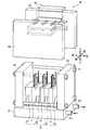
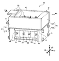
- FIG. 7 is a perspective view for explaining a manufacturing process of the power module.
- the main body portions 11 to 13 (main body portion 10) and the cooling portions 21 to 24 (cooling portion 20) are alternately arranged in the left-right direction and positioned in a close contact state (positioning step).
- the laminated body K composed of the main body 10 and the cooling unit 20 is placed on the metal member 30, a jig (not shown) is installed with the front surface of the metal member 30 as a reference surface, and the main body in the front-rear direction. 10 and the cooling part 20 are positioned.
- the left wall 41 is pressed from the left side against the cooling unit 21 positioned at the left end
- the right wall 42 is pressed from the right side against the cooling unit 24 positioned at the right end.
- the cooling unit 20 is positioned.
- a left and right groove (not shown) is provided on the upper surface of the metal member 30, and the main body 10, the cooling unit 20, and the cylindrical body W are installed on the basis of this groove. Also good. This eliminates the need for the jig described above, thereby improving workability.
- the control terminal 1b When the left wall 41 and the right wall 42 are placed on the metal member 30, the control terminal 1b is inserted through the aforementioned through hole H3, the emitter terminal 1j is inserted through the through hole H4, and the hole H5 (FIG. 4). Through the collector terminal 1i. Further, the collector connection bus bar 51 is fitted into the recess 42c of the right wall 42, and the emitter connection bus bar 52 is fitted into the recess 42d of the right wall 42 (see FIG. 5). By supporting the bus bars 51 and 52 in this way, stress acting on the collector terminal 1i and the emitter terminal 1j (stress caused by the weight of the bus bars 51 and 52) can be suppressed.
- the collector terminal 1i and the collector connection bus bar 51 are welded (for example, spot welding) at the connection portion I (see FIG. 5), and the emitter terminal 1j and the emitter connection bus bar 52 are connected at the connection portion J (see FIG. 6). Weld. Thereby, the main-body part 10 and the bus-bars 51 and 52 are electrically connected (connection process).
- the laminated body K which consists of the main-body part 10 and the cooling part 20 is pressed, and the thermal radiation layers 1e and 1h (refer FIG. 3) and the cooling part 20 contact
- the pressing force by the fastener Q is substantially uniform in the front-rear and up-down directions, a substantially uniform pressing force also acts on the heat radiation layers 1e, 1h and the cooling unit 20 in the surface direction. Therefore, the thermal resistance between the main body 10 and the cooling unit 20 can be reduced.
- one opening of the cooling pipe P2 is connected to the hole H6 provided in the upper surface of the metal member 30, and the cooling pipe P2 is connected to the flow path H1 provided in the cooling unit 20.
- the cooling pipe P ⁇ b> 2 is curved as viewed from the left-right direction so as not to interfere with the metal member 30.
- the above-described cylinder W (see FIG. 4) and the metal member 30 are fixed at a plurality of locations by screw members (not shown). Furthermore, a coating material is applied to the interface in a state where the metal member 30 and the cylindrical body W are in close contact with each other (coating process). As a result, a box B (see FIG. 1) whose upper side is opened is formed by the metal member 30 and the cylinder W.
- the inside of the box B in which the main body part 10, the cooling part 20, the collector connection bus bar 51, and the emitter connection bus bar 52 are arranged is filled with an insulating sealing material G and sealed (sealing process).
- the insulating sealing material G is in a liquid state at the time of filling, since the interface between the metal member 30 and the cylindrical body W is coated as described above, there is no possibility that the insulating sealing material G leaks to the outside.
- the insulating sealing material G for example, silicone gel or potting resin can be used.
- the insulating sealing material G is not limited to the above-described one, and other types of gels or resins may be used.
- the insulating sealing material G is poured until the liquid level becomes higher than the emitter connection bus bar 52 (see FIGS. 5 and 6). By maintaining the power module M filled with the insulating sealing material G in a predetermined temperature range, the insulating sealing material G is solidified.
- the laminated body K is accommodated in the box B (see FIG. 1) composed of the metal member 30 and the cylindrical body W (see FIG. 4), and the cooling water is allowed to flow through the cooling unit 20 so that the main body portion. 10 can be dissipated. Moreover, the main body part 10 and the cooling part 20 are brought into close contact with each other by the pressing force of the fastener Q, and the main body part 10 can be cooled with high efficiency. Further, only the upper side of the box B made of the metal member 30 and the cylinder W is opened, and a coating material is applied to the interface.
- the thin plate-like collector connection bus bar 51 and the emitter connection bus bar 52 are arranged so as to face each other, the magnetic field due to the current flow can be canceled and the inductance between the bus bars 51 and 52 can be reduced. Further, since the bus bars 51 and 52 are sealed by the insulating sealing material G, the distance L1 (see FIG. 5) between the bus bars 51 and 52 in the vertical direction can be made relatively small.
- FIG. 29 is an end view of a power module according to a comparative example. If the power module M1 is not sealed with the insulating sealing material G, the distance L3 between the bus bars 51 and 52 must be increased in order to secure an insulation distance, and the inductance L increases and the power module M1 increases in size. Invite In addition, when the time change (di / dt) of the current due to switching occurs, a spike voltage having a large L (di / dt) is generated, which may cause a problem in the power semiconductor element 1a (see FIG. 3). Furthermore, in order to secure the insulation distance, the diameter of the through hole H4 must be increased (diameter L4: see FIG. 29), and accordingly, the front-rear width of the collector connection bus bar 51 needs to be increased.
- etc. Are sealed with the insulation sealing material G, and the bus bars 51 and 52 can be brought close while ensuring the insulation distance. Therefore, the inductance can be greatly reduced, and the spike voltage during switching can be reduced. Accordingly, even if switching is performed in a short time, the power semiconductor element 1a is not damaged, so that the loss per switching can be reduced and the loss of the entire power module M (that is, the amount of generated heat) can be suppressed. Moreover, the power module M can be reduced in size by arranging the bus bars 51 and 52 in parallel and reducing the distance between the bus bars. As described above, according to the present embodiment, the power module M can be reduced in inductance and size, and can be used for high voltage and large current applications.
- FIG. 8 is an exploded perspective view showing Modification 1 of the power module according to the first embodiment.
- the cooling portions 22 and 23 in which the main body portion 10 is disposed on both the left and right sides are more than the cooling portions 21 and 24 in which the main body portion 10 is disposed on only one side.
- the temperature rises easily. Therefore, the cooling units 22 and 23 may be preferentially cooled as shown in FIG.
- a flow path for guiding the cooling water flowing in via the supply-side pipes P1 and Pa to the cooling pipe P2 corresponding to the cooling units 22 and 23. Is formed. Further, inside the metal member 30, there are formed flow paths (not shown) for guiding the cooling water from the cooling pipes P2 corresponding to the cooling parts 21 and 24 to the discharge side pipes Pb and P3. .
- a cooling pipe (not shown) for guiding the cooling water from the cooling unit 22 to the cooling unit 21 and the cooling water from the cooling unit 23 are guided to the cooling unit 24 on the front side (the back side of the drawing) of the main body.
- a cooling pipe (not shown) is installed.
- the cooling water divided into the pipe Pa flows into the cooling units 22 and 23 through the cooling pipe P2.
- the cooling water that has absorbed heat when flowing through the cooling units 22 and 23 flows into the cooling units 21 and 24 via a cooling pipe (not shown) on the back side of the drawing.
- the cooling water that has further absorbed heat when flowing through the cooling units 21 and 24 merges in the pipe P3 via the pipe Pb. With the configuration shown in FIG. 8, the cooling efficiency of each cooling unit 20 can be increased.
- FIG. 9 is an exploded perspective view showing Modification Example 2 of the power module according to the first embodiment.
- the bus bars 51 and 52 extend in the front-rear direction (in the first embodiment, the bus bars 51 and 52 extend in the left-right direction: see FIG. 4).
- the bus bars 51, 52 and the left wall 41 and the right wall 42 are provided with a gap in the left-right direction in plan view.
- the bus bars 51 and 52 do not contact the left wall 41 and the right wall 42. That is, the drag (reaction force) from the bus bars 51 and 52 does not act on the left wall 41 and the right wall 42, and the laminate K can be sufficiently pressed with a relatively small force (tightening with the fastener Q).
- the bus bars 51 and 52 may be supported by the front wall 43 and the rear wall 44, and the bus bars 51 and 52 may be exposed to the outside through either the left wall 41 or the right wall 42. Even in this case, since the bus bars 51 and 52 do not contact the other of the left wall 41 and the right wall 42, the laminate K can be sufficiently pressed with a relatively small force.
- Second Embodiment the left wall 41 is divided into an insulating member 411 (see FIG. 10) and a pressure member 412, and the right wall 42 is also divided into an insulating member 421 and a pressure member 422. Otherwise, the rest is the same as in the first embodiment. Therefore, a different part from 1st Embodiment is demonstrated and description is abbreviate
- FIG. 10 is an exploded perspective view of the power module according to this embodiment as viewed from the right rear.
- the left wall 41 includes an insulating member 411 on which the bus bars 51 and 52 are installed, and a pressure member 412 that supports the insulating member 411.
- the right wall 42 includes an insulating member 421 and a pressure member 422.
- the pair of pressure members 412 and 422 has a rectangular parallelepiped shape, and is disposed on both sides in the stacking direction (left-right direction) of the stacked body K including the main body 10 and the cooling unit 20.
- the pressing members 412 and 422 are pressed from the left and right by the fastener Q. Thereby, since the laminated body K is pressed so as to be compressed from the left and right, the main body portion 10 and the cooling portion 20 are in close contact with each other. In a state where the pressure members 412 and 422 are fixed to the metal member 30, a coating material is applied to the interface.
- the pressure members 412 and 422 are preferably made of metal (for example, copper). This is to increase the rigidity of the pressure members 412 and 422 and to reduce the bending deformation caused by the pressure, so that the pressing force is uniformly applied to the left and right side surfaces of the laminate K. Thereby, the efficiency of heat exchange between the main body 10 and the cooling unit 20 can be increased. Further, the heat generated in the bus bars 51 and 52 is easily transmitted to the metal member 30 through the pressure members 412 and 422, and the temperature rise of the insulating members 411 and 421 can be suppressed.
- metal for example, copper
- FIG. 11 is an end view of the power module (corresponding to line AA shown in FIG. 1).
- the pair of insulating members 411 and 421 are installed on the pressure members 412 and 422 described above.
- the insulating members 411 and 421 are made of, for example, polyphenylene sulfide resin and have a rectangular parallelepiped shape.
- the left insulating member 411 is integrally formed with the collector connection bus bar 51 and the emitter connection bus bar 52.
- the insulating members 411 and 421 are formed with protrusions 41b and 42b that support the emitter connection bus bar 52.
- the insulating members 411 and 421 are installed on the pressure members 412 and 422 in a state where the fastener Q (see FIG. 10) is installed and the pressure members 412 and 422 are pressed from the left and right.
- the left wall 41 and the right wall 42 (a pair of side walls) are supported by a pair of opposing insulating members 411 and 421 being in close contact with the pair of opposing pressure members 412 and 422. ) Is formed.
- the front wall 43 and the rear wall 44 are installed on the metal member 30.
- a coating material is applied to the interface between the “cylindrical body” (pressure members 412 and 422, insulating members 411 and 421, front wall 43 and rear wall 44) and the metal member 30.
- the “cylinder” and the metal member 30 form a “box” filled with the insulating sealing material G.
- FIG. 12 is an exploded perspective view showing Modification 1 of the power module according to the present embodiment.
- the cooling pipe P2 (not shown in FIG. 10, refer to FIG. 4) having a curved shape when viewed from the left-right direction has been described.
- FIG. Pc and P3 may be installed.
- the supply-side piping P1 is installed on the rear side (the front side of the sheet) of the stacked body K and extends in the left-right direction.
- Four pipes Pc are connected to the pipes P1 so that the cooling water is diverted toward the respective cooling units 20.
- the outlet of each pipe Pc is connected to a hole (not shown) provided in the cooling unit 20.
- the discharge-side pipe P3 is installed on the front side (the back side of the sheet) of the stacked body K and extends in the left-right direction.
- Four pipes (not shown) are connected to the pipes P3 so that the cooling waters flowing out from the respective cooling units 20 are merged.
- the right pressure member 422 is formed with a hole H7 that penetrates the supply-side pipe P1 and a hole H8 that penetrates the discharge-side pipe P3.
- the pipes P1 and P3 are made to pass through the holes H7 and H8, so that the inlet and the outlet face the outside. In this state, the right pressure member 422 can slide in the left-right direction.
- the fastener Q see FIG. 10
- the main body 10 and the cooling unit 20 are brought into close contact with each other.
- the cooling water When the cooling water is supplied through the supply side pipe P1, the cooling water is divided into four pipes Pc.
- the cooling water flowing through the cooling unit 20 absorbs heat from the main body unit 10 and flows into a pipe (not shown) located in front of the stacked body K.
- the cooling water flowing through each pipe joins and is discharged through the discharge pipe P3.
- FIG. 13 is an exploded perspective view showing Modification Example 2 of the power module according to the present embodiment.
- the cooling units 22 and 23 located near the center are preferentially cooled rather than the cooling units 21 and 24 located at the left and right ends. Good.
- the supply-side pipe P1 extending in the left-right direction is connected to the cooling units 22 and 23 via the pipe Pd.
- the discharge pipe P3 extending in the left-right direction is connected to the cooling units 21 and 24 via the pipe Pe.
- Piping (not shown) for supplying the cooling water absorbed by the cooling units 22 and 23 to the cooling units 21 and 24 is installed on the front side (the back side of the drawing) of the cooling units 21 to 24.
- the right pressure member 422 is provided with holes H9 and H10 that allow the pipes P1 and P3 to pass therethrough.
- the cooling efficiency by the cooling unit 20 can be increased by preferentially cooling the cooling units 22 and 23 that are particularly likely to generate heat.
- FIG. 14 is an exploded perspective view showing Modification 3 of the power module according to the present embodiment.
- the front wall 43 and the rear wall 44 made of an insulating material and the pair of left and right insulating members 411 and 421 described in the second embodiment may be integrally molded.
- the manufacturing cost can be reduced.
- the interface between the insulating member 411 and the front wall 43 / rear wall 44 and the interface between the insulating member 421 and the front wall 43 / rear wall 44 described in the second embodiment are eliminated, there is no place to apply the coating material. The production efficiency can be increased.
- the metal member 30 and the pressure members 412 and 422 described in the second embodiment are integrated into a new “metal member 30A”, and the left and right inner portions of the metal member 30A
- the point from which the spring member R was interposed between the wall surface and the laminated body K differs from 2nd Embodiment. Others are the same as in the second embodiment. Therefore, a different part from 2nd Embodiment is demonstrated and description is abbreviate
- FIG. 15 is an exploded perspective view of the power module according to the present embodiment as viewed from the right rear.
- the metal member 30 has a U shape when viewed from the front-rear direction, and is formed so as to be able to accommodate the laminate K.
- the metal member 30 is formed by, for example, a drawing method or an extrusion method.
- the metal member 30A can be formed with high accuracy so that the left wall and the right wall of the metal member 30A are parallel to each other.
- FIG. 16 is an end view of the power module (corresponding to the line AA shown in FIG. 1).
- the spring member R is a leaf spring, for example.
- the two spring members R are interposed between the left and right inner wall surfaces of the metal member 30A and the laminate K.
- the laminated body K is pressed (compressed) from the left and right by the spring member R. .
- the main body 10 and the cooling unit 20 can be brought into close contact with each other, and the cooling efficiency of the main body 10 can be improved.
- the laminated body K and the spring member R are accommodated and positioned in the metal member 30A (positioning step), and the laminated body K is pressed from the left and right by the spring member R (pressing step).
- the collector terminal 1i and the collector connection bus bar 51 are connected, and the emitter terminal 1j and the emitter connection bus bar 52 are connected (connection process).
- the front wall 43 and the rear wall 44 are fitted and fixed to the metal member 30A having a U-shape in the front-rear direction, and the pair of insulating members 411 and 421 to which the bus bars 51 and 52 are attached are mounted on the metal member 30A.
- a coating material is applied to the interfaces of the metal member 30A, the front wall 43, the rear wall 44, and the insulating members 411 and 421 (coating process), and then the insulating sealing material G is filled (sealing process).
- the rigidity of the metal member 30A can be increased compared to the case where these are separate members. . Therefore, even if the spring member R is interposed between the laminate K and the metal member 30A in the left-right direction, the left wall and the right wall of the metal member 30A are not easily deformed. As a result, the pressing force can be applied substantially uniformly in the surface direction of the left and right side surfaces of the laminate K, and the cooling efficiency of the main body 10 can be increased.
- the fourth embodiment is different from the first embodiment (see FIG. 5) in that the cooling unit 20 and the metal member 30 are integrally formed as a “radiating member 60” and a cooling water circulation member 70 is added. Is the same as in the first embodiment. Therefore, a different part from 1st Embodiment is demonstrated and description is abbreviate
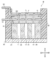
- FIG. 17 is an end view of the power module according to this embodiment (corresponding to line AA shown in FIG. 1).
- the heat radiating member 60 is made of metal (for example, copper), and includes a plate-like support portion 61 (metal member) that supports the cylindrical body W, and cooling portions 62a to 62d that extend upward from the support portion 61. is doing.
- the support portion 61 extends along a horizontal plane and has a rectangular shape in plan view. In the state where the power module M is assembled, the left and right widths of the support portion 61 are set so that the vicinity of both ends protrudes from the left wall 41 and the right wall 42.
- the support portion 61 is provided with a plurality of screw holes through which the screw member T is inserted.
- the cooling units 62 (62a to 62d) each have a rectangular parallelepiped shape, and are formed such that the side surface (substantially the entire surface) of the main body unit 10 is in close contact with the side surface.
- the distance between the cooling units 62 adjacent in the left-right direction corresponds to the left-right width of the main body unit 10. That is, as shown in FIG. 17, the main body 10 is accommodated between the cooling units 62 adjacent in the left-right direction.
- the cooling portion 62a at the left end and the cooling portion 62d at the right end are provided with cuts along the vertical and front / rear surface directions so that the wedge F can be inserted from above.
- the heat dissipation member 60 is formed using, for example, a drawing method or an extrusion method.
- the heat resistance of the cooling unit 62 can be reduced by integrally forming the heat dissipation member 60. That is, the heat absorbed by the cooling unit 62 is easily transmitted toward the support unit 61, and the heat conduction through the cooling unit 62 proceeds smoothly.
- the cooling water circulating member 70 has a thin rectangular parallelepiped shape in the vertical direction, and a plurality of (four in FIG. 17) flow paths H11 are formed in the inside thereof in the front-rear direction. By allowing the cooling water to flow through the flow path H11, the heat radiated from the main body portion 10 to the cooling portion 62 can be released to the outside.
- the cooling water circulation member 70 is installed so as to be in close contact with the lower surface of the support portion 61.
- the heat radiating member 60 is placed on the cooling water circulation member 70, and the heat radiating member 60 is fixed to the metal member 30 by the screw member T (positioning step). By screwing the screw member T in this way, the heat radiating member 60 can be easily positioned in the front-rear and left-right directions.
- a heat conductive sheet such as grease or carbon sheet between the heat radiating member 60 and the cooling water circulation member 70. Thereby, the dimensional variation (thickness variation) of the heat radiation member 60 and the cooling water circulation member 70 is absorbed by the heat conductive sheet, and the thermal resistance can be reduced.
- a metal wedge F is inserted into the notch provided in the cooling unit 62 and the laminate K is pressed from the left and right (pressing step).
- the cooling unit 62 is elastically deformed so as to be pushed left and right.
- the laminated body K including the cooling unit 62 and the main body 10 is pressed (compressed) in the left-right direction, and the main body 10 and the cooling unit 62 are brought into close contact with each other. Therefore, the thermal resistance between the main body 10 and the cooling unit 62 can be reduced.
- the left wall 41 and the right wall 42 on which the bus bars 51 and 52 are installed are installed on both sides of the laminate K, and a front wall 43 (not shown) and a rear wall 44 (not shown) are installed.
- the main body 10 and the bus bars 51 and 52 are electrically connected (connection process).
- the insulating sealing material G is filled (sealing process).
- the positioning process with the cooling water circulation member 70 may be performed after the sealing process.
- the heat radiating member 60 can be easily formed. Further, by fixing the heat radiating member 60 to the cooling water circulation member 70 with the screw member T, the positioning process is easier than in the first embodiment (see FIG. 5) in which positioning is performed using a jig (not shown). Can be done.
- the stacked body K is pressed from the left and right, and the main body unit 10 and the cooling unit 62 are brought into close contact with each other.
- the fastener Q (refer FIG. 7) is used like 1st Embodiment, since the laminated body K can be pressed with a simple structure, the production efficiency of the power module M can be improved.
- the fifth embodiment is different from the fourth embodiment in that a fin 63 is added to the heat radiating member 60 described in the fourth embodiment and is integrally formed to be a new "heat radiating member 60A". This is the same as the fourth embodiment. Therefore, a different part from 4th Embodiment is demonstrated and description is abbreviate
- FIG. 18 is an end view of the power module according to the present embodiment (corresponding to the AA line shown in FIG. 1).
- the heat radiating member 60A is made of metal (for example, copper), and includes a plate-like support portion 61 (metal member) extending along a horizontal plane, cooling portions 62a to 62d extending upward from the support portion 61, and the support portion 61. And a fin 63 extending downward. Similar to the fourth embodiment, the support portion 61 protrudes from the left wall 41 and the right wall 42 at both ends, and a plurality of screw holes are formed.
- the cooling unit 62 (62a to 62d) has a rectangular parallelepiped shape, and is arranged at a predetermined interval (corresponding to the lateral width of the main body unit 10) with another cooling unit 62 adjacent in the left-right direction.
- the cooling parts 62a and 62d at the left and right ends are provided with cuts into which the wedge F is inserted.
- the plurality of fins 63 is a thin plate-like metal extending along the front-rear / up-down direction.
- the heat generated in the main body 10 is radiated by exchanging heat with air through the air cooling fins 63.
- the main body 10 is accommodated between the cooling units 62 adjacent in the left-right direction, and the wedge F is inserted into the notch provided in the cooling unit 62 (positioning step, pressing step).
- the left wall 41 and the right wall 42 on which the bus bars 51 and 52 are installed are installed on both sides of the laminated body including the main body 10 and the cooling unit 62, and a front wall 43 (not shown) and a rear wall are installed. 44 (not shown) is installed.
- the main body portion 10 and the bus bars 51 and 52 are electrically connected.
- the main body portion 10 and the bus bars 51 and 52 are electrically connected.
- the insulating sealing material G is filled (sealing process).
- the support portion 61, the cooling portion 62, and the fin 63 for air cooling are integrally formed to form the heat radiating member 60A, so that the fin 63 is joined to the support portion by caulking or brazing material.
- the thermal resistance can be reduced and the main body 10 can be efficiently cooled.
- the manufacturing process of the heat dissipation member 60A can be simplified.
- the left wall 41 is divided into an insulating member 411 (see FIG. 19) and a pressure member 412, and the right wall 42 is separated from the insulating member 421.
- positioning of the metal member 30B differ, others are the same as that of 1st Embodiment. Therefore, a different part from 1st Embodiment is demonstrated and description is abbreviate
- FIG. 19 is a perspective view of the power module according to this embodiment as viewed from the right rear.
- the power module M includes a main body 10, a cooling unit 20, a metal member 30 ⁇ / b> B that partitions the main body 10 and the cooling unit 20 that are alternately arranged in the left-right direction (see FIGS. 21 and 22), the main body 10 and the cooling.
- Pressure members 412 and 422 that press the portion 20 from the left and right.
- FIG. 20 is an exploded perspective view of the power module as viewed from the right rear.
- Each cooling unit 20 has a rectangular parallelepiped shape, and a flow path for allowing cooling water to flow therethrough is formed.
- the pressure members 412 and 422 are made of metal, for example, and have a rectangular parallelepiped shape having a height substantially equal to that of the cooling unit 20.
- the metal member 30B includes, for example, copper or aluminum having high heat conductivity, and includes a thin plate-like plate-like portion 31 and pocket portions 32 (32a, 32b, 32c) that house the main body portion 10. Yes.
- the plate-like portion 31 has a rectangular shape in plan view and extends along a horizontal plane.
- the pocket portion 32 is a concave portion formed corresponding to the outer shape (cuboid shape) of the main body portion 10, and is recessed downward from the plate-like portion 31.
- the distance between the pocket portions 32 adjacent in the left-right direction is substantially equal to the lateral width of the cooling unit 20.
- the metal member 30B is preferably made of a metal having high thermal conductivity and easy to process, such as copper, aluminum, and alloys thereof.
- the metal member 30B is formed by, for example, drawing / bending.
- FIG. 21 is an end view taken along the line AA shown in FIG.
- the metal member 30 ⁇ / b> B has a bellows-fold shape in a cross-sectional view and functions as a partition plate that partitions the main body 10 and the cooling unit 20.
- the cooling unit 20 and the main body unit 10 accommodated in the pocket unit 32 are alternately arranged in the left-right direction.
- the cooling parts 21 and 22 arranged on both sides of the main body part 11 can exchange heat with the main body part 11 via the pocket part 32a.
- the integrally formed metal member 30B has a function of partitioning the main body 10 and the cooling unit 20 so that heat exchange is possible in a state where the main body 10 and the cooling unit 20 are alternately arranged. .
- the main body 10 faces the upper side (one side) from the metal member 30B in a state where the main body 10 and the cooling unit 20 are alternately arranged and partitioned by the metal member 30B, and the cooling unit 20 is a metal member. It faces the lower side (the other side) from 30B.
- the shape of the metal member 30B is not limited to that shown in FIG. 20 or the like, and may be another shape (uneven shape) having the above-described function. Further, the lower surface of the plate-like portion 31 is in contact with the upper surfaces of the cooling portion 20 and the pressure members 412 and 422.
- the insulating members 411 and 421 shown in FIG. 20 have a thin rectangular parallelepiped shape in the left-right direction.
- the front wall 43 and the rear wall 44 have a thin rectangular parallelepiped shape in the front-rear direction.
- the insulating members 411, 421, the front wall 43, and the rear wall 44 are fixed to each other, thereby forming a cylindrical body W having a rectangular hole H2 in plan view.
- the cylindrical body W is fixed to the plate-like portion 31 in a state where the bus bars 51 and 52 are installed.
- the cooling unit 20 is arranged at a predetermined interval in the left-right direction, pressure members 412 and 422 are arranged on both sides thereof, and positioning is performed using a jig (not shown) (positioning step). At this time, the cooling units 20 adjacent in the left-right direction are separated by a distance substantially equal to the lateral width of the pocket portion 32 (outer shape).
- the metal member 30B is installed from above while using the pressure members 412 and 422 as a reference for positioning in the front-rear and left-right directions. Then, the pocket part 32a fits between the cooling parts 21 and 22, the pocket part 32b fits between the cooling parts 22 and 23, and the pocket part 32c fits between the cooling parts 23 and 24 (see FIG. 21).
- the main body 10 is installed from above with respect to each pocket 32, and the main body 10 is accommodated in the pocket 32.
- the fastener Q (see FIG. 19) is installed, and the pressure members 412 and 422 are tightened from the left and right (pressing step).
- the main body portions 10 and the cooling portions 20 that are alternately arranged with the metal members 30B interposed therebetween are pressed (compressed) from the left and right.
- the cylindrical body W (see FIG. 20) including the insulating members 411, 421, the front wall 43, and the rear wall 44 in a state where the bus bars 51, 52 are installed is placed on the plate-like portion 31.
- the cylindrical body W described above is supported by the pressure members 412 and 422 through the thin metal member 30B.
- the above-mentioned cylinder W, the plate-shaped part 31, and the pressurization members 412 and 422 are fixed.
- these may be fixed using an adhesive, or may be fixed using a fastener such as a bolt.
- a “box” opened upward by the cylindrical body W and the metal member 30B is formed.
- the collector connection bus bar 51 and the collector terminal 1i are connected, and the emitter connection bus bar 52 and the emitter terminal 1j are connected (connection process).
- a coating material is applied to the interface between the plate-shaped portion 31 and the cylindrical body W composed of the left and right insulating members 411, 421, the front wall 43, and the rear wall 44 (coating process).
- the “box” made of the cylindrical body W and the metal member 30B is filled with the insulating sealing material G, and the main body 10, the bus bars 51, 52, and the like are sealed (sealing step).
- the metal member 30B that functions as a partition plate, the cooling unit 20, the pressure members 412, 422, the main body unit 10, the insulating members 411, 421, the front wall 43, and the rear wall 44. Can be completely partitioned in the vertical direction. Therefore, leakage of the insulating sealing material G poured into the “box” made of the cylindrical body W and the metal member 30B can be prevented.
- the metal member 30B according to this embodiment has a thin plate shape (see FIG. 21), and the metal member of the first embodiment (see FIG. 4) in which a cooling water flow path (not shown) is formed. ) And the volume is small. Therefore, the power module M can be reduced in size.
- the coating material may be applied only to the interfaces of the insulating members 411 and 412, the front wall 43, the rear wall 44, and the metal member 30 ⁇ / b> B forming the “box” described above. Workability can be improved. Further, since there is no possibility that the insulating sealing material G leaks to the outside, it is not necessary to extend the front wall 43 and the rear wall 44 below the metal member 30B shown in FIG. That is, the cooling unit 20 is completely opened in the front-rear direction. Therefore, the configuration and arrangement work of the cooling pipe (not shown) connected to the flow path H1 of the cooling unit 20 can be simplified, and workability at the time of manufacturing can be improved.
- the metal member 30B exhibits a bellows fold shape in a side sectional view, and therefore has a relatively small rigidity in the left-right direction. Therefore, when the pressing members 412 and 422 are pressed from the left and right by the fastener Q, the metal member 30B is easily deformed accordingly. Accordingly, the clearance between the inner wall surface of the pocket portion 32 and the main body portion 10 and the clearance between the outer wall surface of the pocket portion 32 and the cooling portion 20 are easily absorbed by the metal member 30B.
- the inner wall surface of the pocket portion 32 and the main body portion 10 are in close contact with each other, the outer wall surface of the pocket portion 32 and the cooling portion 20 are in close contact, and heat exchange between the main body portion 10 and the cooling portion 20 is performed efficiently.
- a high thermal conductive sheet such as grease or carbon sheet is inserted between the pocket portion 32 and the main body portion 10 or between the pocket portion 32 and the cooling portion 20. By doing so, it is possible to reduce thermal resistance.
- FIG. 22 is an end view (corresponding to the line AA shown in FIG. 19) showing a first modification of the power module according to the present embodiment.
- the left pressure member 412, the right pressure member 422, and the bottom wall 45 are integrally formed so as to be U-shaped in cross section.
- a spring member R plate spring
- a spring member R is interposed between the cooling portion 21 at the left end and the pressure member 412
- a spring member R is interposed between the cooling portion 24 at the right end and the pressure member 422.
- the rigidity of the pressure members 412 and 422 can be increased by integrally molding the pressure members 412 and 422 and the bottom wall 45. Therefore, when the spring member R is installed as shown in FIG. 22, the pressing force from the left and right acts on the main body 10 and the cooling unit 20 substantially uniformly. Therefore, the cooling efficiency of the main body 10 can be increased.
- FIG. 23 is an end view (corresponding to the line AA shown in FIG. 19) showing a second modification of the power module according to the present embodiment.
- the pressure member 412 on the left side has an inverted L shape when viewed from the front-rear direction, and has an overhanging portion 412a that projects to the left.
- the overhanging portion 412a is formed with a screw hole along the vertical direction.
- screw holes are also formed in the vicinity of both left and right ends of the metal member 30B, and screw holes to be screwed with the screw member T are also formed in the left and right insulating members 411 and 421.
- the front wall 43 (not shown), the rear wall 44 (not shown), and the left and right insulating members 411 and 421 are integrally formed to form a “cylinder” having a rectangular hole in plan view.
- a “cylinder” having a rectangular hole in plan view.
- the fastener Q (refer FIG. 19) demonstrated in 6th Embodiment becomes unnecessary, the manufacturing cost of the power module M can be reduced.
- the front wall 43, the rear wall 44, and the left and right insulating members 411 and 421 are integrally formed, the number of locations to be coated is reduced as compared with the sixth embodiment, so that workability at the time of manufacturing is improved. Can do.
- the seventh embodiment is different from the sixth embodiment in that the edge of the metal member 30C is raised and the shape / arrangement of the bus bars 51 and 52, but the others are the same as in the sixth embodiment. It is. Therefore, a different part from 6th Embodiment is demonstrated and description is abbreviate
- FIG. 24 is an exploded perspective view of the power module according to this embodiment as viewed from the right rear.
- the metal member 30 ⁇ / b> C includes a plate-like portion 31 extending along a horizontal plane, pocket portions 32 (32 a, 32 b, 32 c) that are recessed downward from the plate-like portion 31, and an edge of the plate-like portion 31.
- a standing portion 33 that rises upward from the top.
- the standing portion 33 has a rectangular frame shape in plan view.
- the standing portion 33 surrounds the cylindrical body W.
- the inner wall surface of the upright part 33 which is square frame shape is adjoining to the outer wall surface of the cylinder W (refer FIG. 25).
- FIG. 25 is an end view of the power module (corresponding to line AA shown in FIG. 19).
- the collector connection bus bar 51 and the emitter connection bus bar 52 are integrally formed with the left insulating member 411 and exposed from the upper surface of the insulating member 411.
- the front and rear widths of the exposed portions of the bus bars 51 and 52 are set so as to ensure an insulation distance in the air.
- the left insulating member 411 has a protrusion 411a that extends in the front-rear direction and protrudes upward.
- a length along the wall surface of the exposed portion of the collector connection bus bar 51 and the sealing portion of the emitter connection bus bar 52 (the portion filled with the insulating sealing material G) is secured. And insulation can be improved.
- the manufacturing process of the power module M is the same as that of 6th Embodiment, description is abbreviate
- the influence of gravity is applied when the coating material is applied to the interface between the cylindrical member W including the insulating members 411 and 421, the front wall 43, and the rear wall 44, and the metal member 30C.
- the coating material applied to the interface enters the gap between the outer wall surface of the cylindrical body W and the inner wall surface of the upright portion 33. Therefore, a coating process can be performed easily and workability at the time of manufacturing the power module M can be improved.
- FIG. 26 is an end view (corresponding to the line AA shown in FIG. 19) showing a first modification of the power module according to the present embodiment.
- the height at which the rising portion 33 of the metal member 30D is raised may be higher than the liquid level of the insulating sealing material G filled in the “box” (the distance shown in FIG. 26). See L5).
- the upper end surface of the upright portion 33 with respect to the entire square frame-like upright portion 33 (including the front side and the rear side) rising from the edge of the plate-like portion 31 of the metal member 30D. Is higher than the liquid level of the insulating sealing material G.
- the metal member 30D By configuring the metal member 30D in this manner, it is assumed that the insulating sealing material G is interposed through a gap between the “cylindrical body” composed of the insulating members 411, 421, the front wall 43, and the rear wall 44 and the metal member 30D. Even if leaks out, there is no possibility that the insulating sealing material G rises beyond the liquid level of the insulating sealing material G shown in FIG. This is because, based on Pascal's principle, a force for equalizing the liquid level of the insulating sealing material G acts by atmospheric pressure. Thus, according to the structure shown in FIG. 26, it can prevent reliably that the insulating sealing material G leaks outside.
- FIG. 27 is an end view (corresponding to line AA shown in FIG. 19) showing a second modification of the power module according to the present embodiment.
- the pressure member 412 on the left side has an inverted L shape when viewed from the front-rear direction, and a screw hole is formed along the up-down direction in the overhanging portion 412a that projects to the left. ing. The same applies to the pressure member 422 on the right side.
- the screw member T As shown in FIG. 27, by installing the screw member T, the pressure members 412 and 422, the metal member 30D, and the cylinder (insulating members 411 and 421, the front wall 43, the rear wall 44) can be easily positioned. Can be fixed.
- the eighth embodiment is different from the seventh embodiment (Modification 2) in which the cooling water is passed through the cooling unit 20 in that a heat sink 80 (see FIG. 28) is installed in the cooling unit 20.
- the rest is the same as in the seventh embodiment (Modification 2). Therefore, a different part from 7th Embodiment (modification 2) is demonstrated, and description is abbreviate
- FIG. 28 is an end view of the power module according to this embodiment (corresponding to line AA shown in FIG. 19).
- the heat sink 80 is provided to radiate the heat absorbed from the cooling unit 20 to the air.
- the heat sink 80 includes a metal (for example, aluminum) having high heat conductivity, and includes a base portion 81 and fins 82.
- Each base portion 81 is a plate-like member that extends downward (on the other side) along the front / rear / up / down surface, and is joined to the lower surface of the cooling portion 20 by caulking or brazing material.
- the fins 82 are installed on the above-described base portion 81 and extend along the horizontal plane so as not to interfere with other fins 82.
- the emitted-heat amount of the main-body part 10 is large, it may replace with the heat sink 80 and you may insert the heat pipe (not shown) for cooling in the up-down direction or the front-back direction.
- the power module M according to the present invention has been described above, but the present invention is not limited to the above-described embodiments, and can be changed as appropriate.
- the present invention is not limited thereto. That is, the number of the main body portions 10 may be appropriately changed according to the energization capacity of the power module M, and the stacked body K may be configured by alternately arranging the main body portions 10 and the cooling portions 20.
- the laminated body K, the left wall 41, and the right wall 42 can be positioned by using a jig (not shown).
- the above embodiments can be appropriately combined.
- the third embodiment (see FIG. 16) may be applied to the fourth embodiment (see FIG. 17). That is, the laminated body K is accommodated in the heat radiating member 60 in which the cooling unit 20 and the metal member 30 are integrally formed, and the spring member R is installed (see FIG. 16). You may make it install in. In this case, there is no need to provide the cooling unit 20 with a flow path for allowing the cooling water to flow, and the configuration of the cooling unit 20 can be simplified.
Abstract
Description
ところで、パワー半導体チップは通電に伴う発熱量が大きいため、パワー半導体チップを冷却して適温に保つことが要請されている。また、パワー半導体チップの小型化も要請されている。
図1は、本実施形態に係るパワーモジュールを右後方から見下ろした斜視図である。なお、図1では、各端子及び各バスバーを封止する絶縁封止材(ゲル)の図示を省略している。
パワーモジュールMは、例えば、高電圧用の電力変換装置(図示せず)に用いられ、外部の制御装置(図示せず)からの指令に応じてスイッチング動作を行うものである。パワーモジュールMは、三つの本体部11~13(図4参照)と、四つの冷却部21~24と、金属部材30と、筒体W(左壁41、右壁42、前壁43、後壁44)と、コレクタ連結バスバー51と、エミッタ連結バスバー52と、を備えている。
図2は、本体部の斜視図である。本体部11は、制御端子1bを介して入力される電気信号に応じて、コレクタ端子1i及びエミッタ端子1jを導通・遮断するものである。なお、図2に示す例では、本体部11が直方体状を呈しているが、本体部11の形状はこれに限定されない。
本体部11は、主に、パワー半導体素子1aと、制御端子1b(図2参照)と、配線層1c,1fと、絶縁層1d,1gと、放熱層1e,1hと、コレクタ端子1iと、エミッタ端子1j(図2参照)と、を有している。なお、本体部11が有するパワー半導体素子1aの数を、通電容量に対応して増加させてもよい。
パワー半導体素子1a(半導体素子)は、例えば、IGBT(Insulated Gate Bipolar Transistor)であり、本体部11に内蔵されている。なお、パワー半導体素子1aの種類はこれに限定されず、MOSFET(Metal-Oxide-Semiconductor Field Effect Transistor)、GTO(Gate Turn-Off thyristor)、ダイオード等、さまざまな素子を用いることができる。
以下では、主にコレクタ側の配線層1c、絶縁層1d、及び放熱層1eについて説明するが、エミッタ側についても同様である。
パワー半導体素子1aと配線層1cとは、例えば、粒径が50μm以下の酸化銀(AgO、Ag2O)又は酸化銅(CuO)の粒子を主体とした接合材料を用いて電気的に接合される。
放熱層1eは、パワー半導体素子1a等で発生する熱を外部に逃がすために設けられ、銅、アルミニウム、又は銅とアルミニウム合金からなる高熱伝導な金属を含んでいる。なお、前記した金属に、モリブデン、タングステン、カーボンを拡散させることで、高熱伝導かつ低熱膨張にすることが好ましい。
樹脂部材1kとして、接着性のあるフェノール系、アクリル系、ポリイミド系、ポリアミドイミド系、エポキシ系、シリコン系、ビスマレイミドトリアジン系、シアネートエステル系等の樹脂を用いることができる。なお、SiO2、Al2O3、AlN、BN等のセラミックスや、ゲル、ゴムを樹脂部材1kに含有させることが好ましい。これによって、樹脂部材1kを低熱膨張とし、パワー半導体素子1aや絶縁層1d,1gに作用する熱応力を低減できる。
図3に示すように、絶縁層1d(1g)の外側に放熱層1e(1h)を設け、さらに樹脂部材1kで封止することで、本体部11の絶縁性・伝熱性を十分に確保できる。なお、図3に示す構成は一例であり、本体部11の構成はこれに限定されない。また、他の本体部12,13(図4参照)も同様の構成を有している。
図4は、パワーモジュールを右後方から見下ろした分解斜視図である。
冷却部21は、本体部11等を冷却するためのものであり、前記した放熱層1eと熱交換可能に配置されている。冷却部21は、伝熱性の高い金属部材(例えば、銅)であり、その外形は直方体状を呈している。その他の冷却部22~24についても同様である。
以下では、本体部11~13をまとめて「本体部10」と記載し、冷却部21~24をまとめて「冷却部20」と記すことがあるものとする。
冷却部20には、冷水を通流させる流路H1(図5参照)が設けられている。前記した流路H1の上流端及び下流端には、それぞれ冷却用パイプP2が接続される(図4参照)。
図4に示す金属部材30は、後記する筒体Wを支持するものであり、上下方向に肉薄の直方体状を呈している。金属部材30は、冷却部20で吸熱した熱を外部に逃がす機能と、筒体Wに密着することで絶縁封止材Gの漏洩を防ぐ機能と、を有している。金属部材30は、銅(Cu)、アルミニウム(Al)、銅とアルミニウムの合金等、成形容易な金属で形成されることが好ましい。
金属部材30には、前記した本体部10及び冷却部20からなる積層体Kが載置される。
筒体W(左壁41、右壁42、前壁43、後壁44)は、平面視で矩形状の孔H2(図1参照)を有しており、前記した金属部材30に密着している。金属部材30に筒体Wが密着することで、一方側(上側)が開放された箱体B(図1参照)が形成される。
左壁41は、コレクタ連結バスバー51を支持する突起部41aと、エミッタ連結バスバー52を支持する突起部41bと、を有している。各突起部41a,41bは右方に向かって突出しており、前後方向に延びている。突起部41a,41bは、後記する絶縁封止材Gで封止された状態において、バスバー51,52の絶縁距離を確保できるように形成されている。なお、右壁42に形成された突起部42a,42bについても同様である。
なお、右壁42に設けられた突起部42a、42bの上方には、各バスバー51,52の右端が嵌め込まれる凹部42c,42dが形成されている。
図4に示すコレクタ連結バスバー51(バスバー)は、コレクタ端子1iと電気的に接続される金属部材である。コレクタ連結バスバー51は、電気抵抗を小さくし、大電流に伴うジュール熱を低減するために、薄板状を呈している。
コレクタ連結バスバー51には、制御端子1bを外部に引きだすための貫通孔H3(6個)と、エミッタ端子1jを上方に引き出すための貫通孔H4(3個)と、コレクタ端子1iとコレクタ連結バスバー51とを接続するための接続部I(3個)と、が設けられている。
特に、エミッタ端子1jが引き出される貫通孔H4の孔径は、後記する絶縁封止材Gで封止された状態で、エミッタ端子1jとコレクタ連結バスバー51との絶縁距離を確保できるように設定されている。
図6は、図1に示すB-B線で切断した端面図である。
エミッタ連結バスバー52(バスバー)は、エミッタ端子1jを介して電流が流れる薄板状の金属部材であり、エミッタ端子1jと電気的に接続される。エミッタ連結バスバー52には、制御端子1bを引き出すための貫通孔H3(6個:図4参照)と、エミッタ端子1jとエミッタ連結バスバー52とを接続するための接続部J(3個)と、が設けられている。
図4~図6に示すように、コレクタ連結バスバー51とエミッタ連結バスバー52とは、互いに平行に配置され、一方に流れる電流と他方に流れる電流とが逆向きになるように配置されている。これによって、各バスバー51,52に流れる電流によって発生する磁界が打ち消され、インダクタンスを低減できる。
また、後記するように、コレクタ連結バスバー51及びエミッタ連結バスバー52も、絶縁封止材Gで封止される。したがって、バスバー51,52との距離L1(図5参照)を比較的小さくしても(つまり、インダクタンスを低減させても)、放電が起こるおそれはない。
なお、バスバー51,52を左壁41と一体成形せずに別体とし、かしめ(図示せず)によってバスバー51,52を左壁41に設置するようにしてもよい。
例えば、同期した制御信号が各制御端子1bから入力されると、各パワー半導体素子1a(図3参照)も同期してオン/オフ動作し、これに伴う大電流がコレクタ連結バスバー51及びエミッタ連結バスバー52に流れる。この場合、パワーモジュールM全体が、一つの大きなスイッチング回路として機能する。なお、パワーモジュールMの用途は、前記した例に限定されない。
図7は、パワーモジュールの製造工程を説明するための斜視図である。
まず、本体部11~13(本体部10)と冷却部21~24(冷却部20)とを左右方向で交互に配置し、密着させた状態で位置決めする(位置決め工程)。例えば、本体部10及び冷却部20からなる積層体Kを金属部材30の上に載置し、金属部材30の前面を基準面として治具(図示せず)を設置し、前後方向で本体部10及び冷却部20を位置決めする。
次に、左端に位置する冷却部21に対して左側から左壁41を押し当て、右端に位置する冷却部24に対して右側から右壁42を押し当てることで、左右方向で本体部10及び冷却部20を位置決めする。
また、コレクタ連結バスバー51を右壁42の凹部42cに嵌め込み、エミッタ連結バスバー52を右壁42の凹部42dに嵌め込む(図5参照)。このようにバスバー51,52を支持することで、コレクタ端子1i及びエミッタ端子1jに作用する応力(バスバー51,52の重量に伴って生じる応力)を抑制できる。
なお、前後・上下方向において締結具Qによる押圧力が略均一であるため、放熱層1e,1hと冷却部20にも、その面方向において略均一な押圧力が作用する。したがって、本体部10と冷却部20との間の熱抵抗を低減できる。
なお、前記した接続工程、押圧工程、パイプ設置工程の順序を適宜入れ替えてもよい。
絶縁封止材Gは、その液面がエミッタ連結バスバー52よりも高くなるまで注ぎ込まれる(図5、図6参照)。絶縁封止材Gが充填されたパワーモジュールMを所定の温度範囲で維持することによって、絶縁封止材Gが固相化する。
本実施形態によれば、金属部材30及び筒体W(図4参照)からなる箱体B(図1参照)に積層体Kを収容し、冷却部20に冷水を通流させることで本体部10を放熱させることができる。また、締結具Qによる押圧力によって本体部10と冷却部20とを密着させ、本体部10を高効率で冷却できる。
また、金属部材30及び筒体Wからなる箱体Bは上方のみが開放され、その界面にはコーティング材が塗布される。したがって、箱体Bの収容空間に注ぎ込まれる絶縁封止材Gが外部に漏れるおそれはなく、コレクタ端子1i、エミッタ端子1j、及びバスバー51,52を絶縁封止材Gで適切に封止できる。
また、前記した各製造工程では複雑な作業を要しないため、製造時の作業性を向上させることができる。
仮に、絶縁封止材GでパワーモジュールM1を封止しない場合、絶縁距離を確保するためにバスバー51,52間の距離L3を大きくせざるを得ず、インダクタンスLの増加及びパワーモジュールM1の大型化を招く。なお、スイッチングによる電流の時間変化(di/dt)が生じると、L(di/dt)の大きなスパイク電圧が発生し、パワー半導体素子1a(図3参照)に不具合が生じるおそれがある。さらに、絶縁距離を確保するために貫通孔H4の径を大きくせざるを得ず(径L4:図29参照)、これに伴ってコレクタ連結バスバー51の前後幅を大きくする必要が生じる。
このように本実施形態によれば、パワーモジュールMの低インダクタンス化及び小型化を図り、高電圧・大電流用途でも対応可能にすることができる。
図8は、第1実施形態に係るパワーモジュールの変形例1を示す分解斜視図である。
それぞれの本体部10の発熱量が略同一である場合、左右両側に本体部10が配置される冷却部22,23の方が、片側のみに本体部10が配置される冷却部21,24よりも昇温しやすい。そこで、図8に示すように冷却部22,23を優先的に冷却するようにしてもよい。
なお、本体部の前側(紙面奥側)には、冷却部22からの冷却水を冷却部21に導く冷却用パイプ(図示せず)と、冷却部23からの冷却水を冷却部24に導く冷却用パイプ(図示せず)と、が設置されている。
図8に示す構成によって、各冷却部20の冷却効率を高めることができる。
図9は、第1実施形態に係るパワーモジュールの変形例2を示す分解斜視図である。
図9に示す例では、バスバー51,52が前後方向に延びている(第1実施形態では、バスバー51,52が左右方向に延びていた:図4参照)。なお、バスバー51,52と、左壁41及び右壁42と、は平面視において左右方向で隙間が設けられている。
なお、前壁43及び後壁44によってバスバー51,52を支持し、左壁41及び右壁42のいずれか一方を介してバスバー51,52を外部に露出させるようにしてもよい。この場合でも、左壁41及び右壁42のうち他方にバスバー51,52が接触しないため、比較的小さな力で積層体Kを十分に押圧できる。
第2実施形態は、左壁41を絶縁部材411(図10参照)と加圧部材412とに分割し、右壁42も絶縁部材421と加圧部材422とに分割した点が第1実施形態と異なるが、その他は第1実施形態と同様である。したがって、第1実施形態と異なる部分について説明し、重複する部分については説明を省略する。
図10は、本実施形態に係るパワーモジュールを右後方から見下ろした分解斜視図である。左壁41は、バスバー51,52が設置される絶縁部材411と、この絶縁部材411を支持する加圧部材412と、を有している。右壁42も同様に、絶縁部材421と、加圧部材422と、を有している。
加圧部材412,422が金属部材30に固定された状態において、その界面にコーティング材が塗布される。
締結具Q(図10参照)を設置して加圧部材412,422を左右から押圧した状態で、絶縁部材411,421を加圧部材412,422の上に設置する。図11に示すように、相対する一対の絶縁部材411,421が、相対する一対の加圧部材412,422に密着した状態で支持されることで、左壁41及び右壁42(一対の側壁)が形成される。
次に、図10に示すように、前壁43及び後壁44(別の側壁)を金属部材30に設置する。そして、「筒体」(加圧部材412,422、絶縁部材411,421、前壁43、後壁44)と金属部材30との界面にコーティング材を塗布する。前記した「筒体」と金属部材30とによって、絶縁封止材Gが充填される「箱体」が形成される。
本実施形態によれば、締結具Qによって加圧部材412,422が左右方向で押圧された場合、バスバー51,52からの抗力(反力)によって、前記した押圧が妨げられることがない。締結具Qの設置時、絶縁部材411,421は加圧部材412,422に固定されていないからである。したがって、比較的小さな力で積層体Kを適切に押圧できる。
また、バスバー51,52による抗力を受けないため、締結具Qによる左右方向の押圧力が積層体Kの左右側面に対して均一に作用する。したがって、本体部10と冷却部20とを密着させ、両者が熱交換する際の熱抵抗を低減できる。
図12は、本実施形態に係るパワーモジュールの変形例1を示す分解斜視図である。
第1、第2実施形態では、左右方向から視て湾曲状を呈する冷却用パイプP2(図10では図示省略、図4参照)を用いる場合について説明したが、図12に示すように配管P1,Pc,P3を設置してもよい。
同様に、排出側の配管P3は、積層体Kの前側(紙面奥側)に設置され、左右方向に延びている。配管P3には、それぞれの冷却部20から流出する冷却水を合流させるように、4本の配管(図示せず)が接続されている。
右側の加圧部材422には、供給側の配管P1を貫通させる孔H7と、排出側の配管P3を貫通させる孔H8と、が形成されている。
図12に示すように各配管を配置することで、金属部材30の内部に流路を設ける必要がなくなり、金属部材30を製造する際の手間を省くことができる。
図13は、本実施形態に係るパワーモジュールの変形例2を示す分解斜視図である。
第1実施形態の変形例1(図8参照)と同様に、左右両端に位置する冷却部21,24よりも、中央付近に位置する冷却部22,23を優先的に冷却するようにしてもよい。
このように、特に発熱しやすい冷却部22,23を優先的に冷却することで、冷却部20による冷却効率を高めることができる。
図14は、本実施形態に係るパワーモジュールの変形例3を示す分解斜視図である。
図14に示すように、絶縁材料で構成された前壁43及び後壁44と、第2実施形態で説明した左右一対の絶縁部材411,421と、を一体成型してもよい。
パワーモジュールMをこのように構成することで、製造コストを低減できる。また、第2実施形態で説明した絶縁部材411と前壁43・後壁44との界面、絶縁部材421と前壁43・後壁44との界面がなくなるため、コーティング材を塗布すべき箇所が少なくなり、生産効率を高めることができる。
第3実施形態は、第2実施形態で説明した金属部材30と加圧部材412,422とを一体化させて、新たに「金属部材30A」とした点と、この金属部材30Aの左右の内壁面と積層体Kとの間にバネ部材Rを介在させた点が、第2実施形態とは異なる。なお、その他は第2実施形態と同様である。したがって、第2実施形態と異なる部分について説明し、重複する部分については説明を省略する。
図15は、本実施形態に係るパワーモジュールを右後方から見下ろした分解斜視図である。図15に示すように、金属部材30は、前後方向から視てU字状を呈しており、積層体Kを収容可能に形成されている。金属部材30は、例えば、引き抜き法や押し出し法によって成型される。これによって、金属部材30Aの左壁と右壁とが互いに平行となるように、高精度で金属部材30Aを形成できる。
まず、金属部材30Aに積層体K及びバネ部材Rを収容して位置決めし(位置決め工程)、バネ部材Rによって積層体Kを左右から押圧する(押圧工程)。次に、コレクタ端子1iとコレクタ連結バスバー51とを接続し、エミッタ端子1jとエミッタ連結バスバー52とを接続する(接続工程)。
続いて、前後方向でU字状を呈する金属部材30Aに前壁43及び後壁44を嵌め込んで固定し、バスバー51,52が取り付けられた一対の絶縁部材411,421を金属部材30Aの上に固定する。次に、金属部材30A、前壁43、後壁44、及び絶縁部材411,421の界面にコーティング材を塗布した後(コーティング工程)、絶縁封止材Gを充填する(封止工程)。
本実施形態によれば、金属部材30Aの左壁、底壁、及び右壁が一体形成されているため、これらが別部材である場合と比較して、金属部材30Aの剛性を高めることができる。したがって、左右方向で積層体Kと金属部材30Aとの間にバネ部材Rを介在させても、金属部材30Aの左壁及び右壁が変形しにくくなる。その結果、積層体Kの左右側面の面方向において押圧力を略均一に作用させ、本体部10の冷却効率を高めることができる。
第4実施形態は、冷却部20及び金属部材30を一体形成して「放熱部材60」とし、さらに冷却水循環部材70を追加した点が第1実施形態(図5参照)とは異なるが、その他は第1実施形態と同様である。したがって、第1実施形態と異なる部分について説明し、重複する部分については説明を省略する。
図17は、本実施形態に係るパワーモジュールの端面図(図1に示すA-A線に対応)である。放熱部材60は、金属製(例えば、銅)であり、筒体Wを支持する板状の支持部61(金属部材)と、この支持部61から上方に延びる冷却部62a~62dと、を有している。支持部61は、水平面に沿って延びており、平面視で矩形状を呈している。パワーモジュールMを組み立てた状態で、その両端付近が左壁41及び右壁42から突出するように、支持部61の左右幅が設定されている。支持部61には、ネジ部材Tを挿通させるためのネジ孔が複数設けられている。
なお、本実施形態では、冷却水を通流させる流路を冷却部62に設ける必要はなく、冷却部62の製造工程を簡単化できる。
冷却水循環部材70の上に放熱部材60を載置し、ネジ部材Tによって放熱部材60を金属部材30に固定する(位置決め工程)。このようにネジ部材Tを螺合することで、前後・左右方向において放熱部材60を容易に位置決めできる。
なお、放熱部材60と冷却水循環部材70との間にグリース、カーボンシート等の熱伝導シート(図示せず)を介在させることが好ましい。これによって、放熱部材60及び冷却水循環部材70の寸法バラつき(厚さバラつき)を熱伝導シートで吸収し、熱抵抗を低減できる。
次に、支持部61、左壁41、右壁42、前壁43、及び後壁44の界面にコーティング材を塗布した後(コーティング工程)、絶縁封止材Gを充填する(封止工程)。
なお、冷却水循環部材70との位置決め工程は、封止工程の後でも構わない。これによって、パワーモジュールMを単体で製造することが可能となり、生産性を向上させることができる。
本実施形態によれば、放熱部材60に冷却水の流路を設ける必要がないため、放熱部材60を容易に成形できる。また、ネジ部材Tによって放熱部材60を冷却水循環部材70に固定することで、治具(図示せず)を用いて位置決めする第1実施形態(図5参照)と比較して、位置決め工程を容易に行うことができる。
第5実施形態は、第4実施形態で説明した放熱部材60にフィン63を追加して一体形成し、新たに「放熱部材60A」とした点が第4実施形態とは異なるが、その他は第4実施形態と同様である。したがって、第4実施形態と異なる部分について説明し、重複する部分については説明を省略する。
図18は、本実施形態に係るパワーモジュールの端面図(図1に示すA-A線に対応)である。放熱部材60Aは、金属製(例えば、銅)であり、水平面に沿って延びる板状の支持部61(金属部材)と、支持部61から上側に延びる冷却部62a~62dと、支持部61から下側に延びるフィン63と、を有している。
第4実施形態と同様に、支持部61は、その両端付近が左壁41及び右壁42から突出しており、複数のネジ孔が形成されている。冷却部62(62a~62d)は、直方体状を呈しており、左右方向において隣り合う他の冷却部62と所定間隔(本体部10の横幅に対応)を空けて配置されている。左右両端の冷却部62a,62dには、クサビFが差し込まれる切込みが設けられている。
左右方向において隣り合う冷却部62の間に本体部10を収容し、冷却部62に設けられた切込みにクサビFを差し込む(位置決め工程、押圧工程)。次に、バスバー51,52が設置された左壁41及び右壁42を、本体部10及び冷却部62からなる積層体の両脇に設置し、さらに前壁43(図示せず)及び後壁44(図示せず)を設置する。
次に、支持部61、左壁41、右壁42、前壁43、及び後壁44の界面にコーティング材を塗布した後(コーティング工程)、絶縁封止材Gを充填する(封止工程)。
本実施形態によれば、支持部61、冷却部62、及び空冷用のフィン63を一体形成して放熱部材60Aとすることで、かしめ又はろう材で支持部にフィン63を接合する場合と比較して熱抵抗を低減し、本体部10を効率的に冷却できる。また、冷却水を通流させるための流路を放熱部材60Aに設ける必要がないため、放熱部材60Aの製造工程を簡単化できる。
第6実施形態は、第1実施形態(図4参照)と比較して、左壁41を絶縁部材411(図19参照)と加圧部材412とに分割し、右壁42を絶縁部材421と加圧部材422とに分割した点、及び金属部材30Bの構成・配置が異なるが、その他については第1実施形態と同様である。したがって、第1実施形態と異なる部分について説明し、重複する部分については説明を省略する。
図19は、本実施形態に係るパワーモジュールを右後方から見下ろした斜視図である。
パワーモジュールMは、本体部10と、冷却部20と、左右方向で交互に配置された本体部10及び冷却部20を仕切る金属部材30Bと(図21、図22参照)、本体部10及び冷却部20を左右から押圧する加圧部材412,422と、を備えている。
それぞれの冷却部20は、直方体状を呈しており、冷却水を通流させるための流路が形成されている。加圧部材412,422は、例えば、金属製であり、冷却部20と略等しい高さの直方体状を呈している。
また、本体部10と冷却部20とが交互に配置され、かつ、金属部材30Bによって仕切られた状態で、本体部10は金属部材30Bから上側(一方側)に臨み、冷却部20は金属部材30Bから下側(他方側)に臨んでいる。なお、金属部材30Bの形状は図20等に示すものに限定されず、前記した機能を有する別の形状(凹凸状)としてもよい。
また、板状部31の下面は、冷却部20及び加圧部材412,422の上面に当接している。
まず、左右方向で所定間隔を空けて冷却部20を配置し、その両脇に加圧部材412,422を配置し、治具(図示せず)を用いて位置決めする(位置決め工程)。このとき、左右方向で隣り合う冷却部20を、ポケット部32(外形)の横幅と略等しい距離だけ離しておく。
次に、前後・左右方向の位置決めをする際の基準として加圧部材412,422を用いつつ、金属部材30Bを上方から設置する。そうすると、冷却部21,22の間にポケット部32aが、冷却部22,23の間にポケット部32bが、冷却部23,24の間にポケット部32cが嵌まり込む(図21参照)。
そして、前記した筒体W、板状部31、及び加圧部材412,422を固定する。例えば、接着剤を用いてこれらを固着させてもよいし、ボルト等の締結具を用いて固定してもよい。その結果、筒体Wと、金属部材30Bと、によって上方に開放された「箱体」が形成される。
次に、前記した筒体W及び金属部材30Bからなる「箱体」に絶縁封止材Gを充填し、本体部10、バスバー51,52等を封止する(封止工程)。
本実施形態によれば、仕切り板として機能する金属部材30Bを設置することで、冷却部20・加圧部材412,422と、本体部10・絶縁部材411,421・前壁43・後壁44と、を上下方向において完全に仕切ることができる。したがって、筒体W及び金属部材30Bからなる「箱体」に注ぎ込まれる絶縁封止材Gの漏洩を防止できる。
また、本実施形態に係る金属部材30Bは薄板状を呈しており(図21参照)、内部に冷却水の流路(図示せず)が形成される第1実施形態の金属部材(図4参照)と比較して体積が小さい。したがって、パワーモジュールMを小型化できる。
また、絶縁封止材Gが外部に漏れるおそれはないため、図20に示す金属部材30Bよりも下方まで前壁43及び後壁44を延ばす必要がない。つまり、前後方向において冷却部20が完全に開放された状態になる。したがって、冷却部20の流路H1に接続される冷却用パイプ(図示せず)の構成及び配設作業を簡単にすることができ、製造時における作業性を高めることができる。
これによって、ポケット部32の内壁面と本体部10とのクリアランスや、ポケット部32の外壁面と冷却部20とのクリアランスが金属部材30Bで吸収されやすくなる。その結果、ポケット部32の内壁面と本体部10とが密着するとともに、ポケット部32の外壁面と冷却部20とが密着し、本体部10と冷却部20との熱交換を効率的に行うことができる。
また、第1実施形態と同様に、ポケット部32と本体部10との間や、ポケット部32と冷却部20との間に、グリース、カーボンシート等の高熱伝導シート(図示せず)を挿入することで、熱抵抗を低減することが可能である。
図22は、本実施形態に係るパワーモジュールの変形例1を示す端面図(図19に示すA-A線に対応)である。図22に示す例では、左側の加圧部材412、右側の加圧部材422、及び底壁45が、断面視U字状となるように一体形成されている。また、左端の冷却部21と加圧部材412との間にバネ部材R(板バネ)が介在し、右端の冷却部24と加圧部材422との間にバネ部材Rが介在している。
なお、本実施形態では、第6実施形態で説明した締結具Q(図19参照)を設置する必要はない。
図23は、本実施形態に係るパワーモジュールの変形例2を示す端面図(図19に示すA-A線に対応)である。図23に示すように、左側の加圧部材412は、前後方向から視て逆L字状を呈しており、左方に張り出した張出部412aを有している。この張出部412aには、上下方向に沿うネジ孔が形成されている。右側の加圧部材422についても同様である。
また、金属部材30Bの左右両端付近にもネジ孔が形成され、左右の絶縁部材411,421にもネジ部材Tと螺合するネジ穴が形成されている。
さらに、前壁43、後壁44、及び左右の絶縁部材411,421が一体形成されることで、第6実施形態と比較してコーティングすべき箇所が減るため、製造時における作業性を高めることができる。
第7実施形態は、第6実施形態と比較して、金属部材30Cの縁が起立している点と、バスバー51,52の形状・配置と、が異なるが、その他は第6実施形態と同様である。したがって、第6実施形態と異なる部分について説明し、重複する部分については説明を省略する。
図24は、本実施形態に係るパワーモジュールを右後方から見下ろした分解斜視図である。図24に示すように、金属部材30Cは、水平面に沿って延びる板状部31と、板状部31から下方に凹むポケット部32(32a,32b,32c)と、この板状部31の縁から上方に起立する起立部33と、を有している。
起立部33は、平面視で四角枠状を呈している。絶縁部材411,421、前壁43、後壁44からなる筒体Wを金属部材30Cに設置した状態において、起立部33は筒体Wを囲んでいる。なお、四角枠状である起立部33の内壁面は、筒体Wの外壁面に近接している(図25参照)。
なお、パワーモジュールMの製造工程は、第6実施形態と同様であるから説明を省略する。
本実施形態によれば、コレクタ連結バスバー51及びエミッタ連結バスバー52を左側の絶縁部材411の上面から露出させることで、複数のパワーモジュールMの接続関係を考慮してバスバー51,52を横並びで引き出したほうが良い場合にも対応できる。
図26は、本実施形態に係るパワーモジュールの変形例1を示す端面図(図19に示すA-A線に対応)である。図26に示すように、金属部材30Dの起立部33を立ち上げる高さを、「箱体」に充填される絶縁封止材Gの液面よりも高くしてもよい(図26に示す距離L5を参照)。なお、図26の端面図には表れていないが、金属部材30Dの板状部31の縁から立ち上がる四角枠状の起立部33全体(前側、後側を含む)に関して、起立部33の上端面が絶縁封止材Gの液面よりも高くなっている。
図27は、本実施形態に係るパワーモジュールの変形例2を示す端面図(図19に示すA-A線に対応)である。図27に示すように、左側の加圧部材412は、前後方向から視て逆L字状を呈しており、左方に張り出した張出部412aには、上下方向に沿うネジ孔が形成されている。右側の加圧部材422についても同様である。図27に示すように、ネジ部材Tを設置することで、加圧部材412,422、金属部材30D、及び筒体(絶縁部材411,421、前壁43、後壁44)を容易に位置決めし、固定できる。
第8実施形態は、冷却部20に冷却水を通流させる構成としていた第7実施形態(変形例2)と比較して、冷却部20にヒートシンク80(図28参照)を設置する点が異なるが、その他は第7実施形態(変形例2)と同様である。したがって、第7実施形態(変形例2)と異なる部分について説明し、重複する部分については説明を省略する。
図28は、本実施形態に係るパワーモジュールの端面図(図19に示すA-A線に対応)である。ヒートシンク80は、冷却部20から吸熱した熱を空気に放熱するために設けられる。ヒートシンク80は、伝熱性の高い金属(例えば、アルミニウム)を含んでおり、基部81と、フィン82と、を有している。それぞれの基部81は、前後・上下方向の面に沿って下方(他方側)に延びる板状部材であり、かしめ又はろう材で冷却部20の下面に接合される。
なお、本体部10の発熱量が大きい場合、ヒートシンク80に代えて、冷却用のヒートパイプ(図示せず)を上下方向又は前後方向に挿入してもよい。
本実施形態によれば、冷却水を通流させるための流路を冷却部20に設ける必要がないため、冷却部20の製造工程を簡単化できる。また、図28に示すように多数のフィン82を設けることで、フィン82と空気との接触面積を確保し、フィン82から空気中に放熱する際の伝熱効率を高めることができる。
以上、本発明に係るパワーモジュールMについて説明したが、本発明は前記した各実施形態に限定されるものではなく、適宜変更できる。
例えば、前記各実施形態では、パワーモジュールMが三つの本体部10を備える場合について説明したが、これに限らない。すなわち、パワーモジュールMの通電容量等に応じて、本体部10の数を適宜変更し、本体部10と冷却部20とを交互に配置して積層体Kを構成するようにしてもよい。
10,11,12,13 本体部
1a パワー半導体素子(半導体素子)
1b 制御端子
1e,1h 放熱層
1i コレクタ端子(パワー端子)
1j エミッタ端子(パワー端子)
20,21,22,23,24,62,62a,62b,62c,62d 冷却部
30,30A,30B,30C,30D,40, 金属部材
31 板状部
32,32a,32b,32c ポケット部
33 起立部
41 左壁(一対の側壁、筒体)
42 右壁(一対の側壁、筒体)
43 前壁(別の側壁、筒体)
44 後壁(別の側壁、筒体)
412,422 加圧部材
411,421 絶縁部材
51 コレクタ連結バスバー(バスバー)
52 エミッタ連結バスバー(バスバー)
60,60A 放熱部材
61 支持部
63 フィン
70 冷却水循環部材
80 ヒートシンク
81 基部
82 フィン
K 積層体
W 筒体
B 箱体
H1 流路
G 絶縁封止材
Claims (16)
- 半導体素子と、前記半導体素子に接続される制御端子と、前記制御端子への電気信号に応じた電流が流れるパワー端子と、放熱層と、を有する本体部と、
前記放熱層と熱交換可能に配置され、前記本体部を冷却する冷却部と、
前記パワー端子に接続されるバスバーと、
少なくとも前記バスバーとの接触箇所が絶縁性である筒体と、
前記筒体を支持する金属部材と、を備え、
前記金属部材に前記筒体が密着することで、一方側が開放された箱体が形成され、
前記箱体の中に、少なくとも前記本体部及び前記バスバーが配置され、
前記制御端子及び前記パワー端子は、前記半導体素子から前記一方側に延びており、
前記箱体の内部に絶縁封止材が充填されることで、前記本体部及び前記バスバーが封止されること
を特徴とするパワーモジュール。 - 前記本体部と、前記冷却部と、が密着した状態で交互に配置されてなる積層体を備え、
前記箱体の中に前記積層体が収容されること
を特徴とする請求項1に記載のパワーモジュール。 - 前記筒体は、
前記バスバーが設置される絶縁部材と、
前記積層体の積層方向の両側に配置され、前記積層体を挟んで加圧する加圧部材と、を備えること
を特徴とする請求項2に記載のパワーモジュール。 - 前記加圧部材と、前記加圧部材によって支持される前記絶縁部材と、を有する一対の側壁と、
前記一対の側壁に取り付けられることで、当該一対の側壁とともに前記筒体を形成する別の側壁と、を備えること
を特徴とする請求項3に記載のパワーモジュール。 - 前記冷却部と、前記金属部材と、が一体形成されてなる放熱部材と、
前記放熱部材に設置され、冷却水が通流する流路を有する冷却水循環部材と、を備えること
を特徴とする請求項2に記載のパワーモジュール。 - 前記冷却部と、前記金属部材と、空冷用のフィンと、が一体形成されてなる放熱部材を備え、
前記フィンは、前記一方側とは反対の他方側に延びていること
を特徴とする請求項2に記載のパワーモジュール。 - 前記金属部材は、
前記一方側とは反対の他方側に凹み、前記本体部を収容するポケット部を有し、
前記冷却部と、前記ポケット部に収容された前記本体部と、が交互に配置され、
前記本体部の両側に配置される前記冷却部は、前記ポケット部を介して前記本体部と熱交換可能であること
を特徴とする請求項1に記載のパワーモジュール。 - 前記金属部材は、
平面視で前記筒体を囲み、前記一方側に向けて立ち上がる起立部を有すること
を特徴とする請求項7に記載のパワーモジュール。 - 前記起立部が前記一方側に向けて立ち上がる高さは、前記箱体の中に充填される前記絶縁封止材の液面よりも高いこと
を特徴とする請求項8に記載のパワーモジュール。 - 交互に配置される前記本体部及び前記冷却部のうち、両端の前記冷却部を挟んで加圧する加圧部材を備えること
を特徴とする請求項7から請求項9のいずれか一項に記載のパワーモジュール。 - 前記冷却部は、
自身の内部に冷却水を通流させるための流路を有すること
を特徴とする請求項7に記載のパワーモジュール。 - 前記冷却部の前記他方側に設置され、前記冷却部から吸熱した熱を空気に放熱するヒートシンクを備えること
を特徴とする請求項7に記載のパワーモジュール。 - 前記絶縁封止材は、ゲル又はレジンであること
を特徴とする請求項1に記載のパワーモジュール。 - 半導体素子と、前記半導体素子に接続される制御端子と、前記制御端子への電気信号に応じた電流が流れるパワー端子と、放熱層と、を有する本体部と、
前記本体部を冷却する冷却部と、
前記本体部と前記冷却部とが交互に配置された状態で、前記本体部と前記冷却部とを熱交換可能に仕切るための、一体的に形成された金属部材と、を備え、
前記本体部と前記冷却部とが交互に配置され、かつ、前記金属部材によって仕切られた状態で、
前記本体部は、前記金属部材から一方側に臨み、
前記冷却部は、前記金属部材から前記一方側とは反対の他方側に臨むこと
を特徴とするパワーモジュール。 - 半導体素子と、前記半導体素子に接続される制御端子と、前記制御端子への電気信号に応じた電流が流れるパワー端子と、放熱層と、を有する本体部と、
前記放熱層と熱交換可能に配置され、前記本体部を冷却する冷却部と、
を密着させた状態で交互に配置して位置決めする位置決め工程と、
前記パワー端子と、バスバーと、を接続する接続工程と、
少なくとも前記バスバーとの接触箇所が絶縁性である筒体と、前記筒体を支持する金属部材と、を密着させてコーティングし、一方側が開放された箱体を形成するコーティング工程と、
前記本体部、前記冷却部、及び前記バスバーが配置された前記箱体の内部に絶縁封止材を充填して封止する封止工程と、を含み、
前記制御端子及び前記パワー端子は、前記半導体素子から前記一方側に延びていること
を特徴とするパワーモジュールの製造方法。 - 半導体素子と、前記半導体素子に接続される制御端子と、前記制御端子への電気信号に応じた電流が流れるパワー端子と、放熱層と、を有する本体部と、
前記放熱層と熱交換可能に配置され、前記本体部を冷却する冷却部と、
の間に金属部材を介在させ、前記冷却部と、前記金属部材のポケット部に収容された前記本体部と、を交互に配置して位置決めする位置決め工程と、
前記パワー端子と、バスバーと、を接続する接続工程と、
少なくとも前記バスバーとの接触箇所が絶縁性である筒体と、前記筒体を支持する前記金属部材と、を密着させてコーティングし、一方側が開放された箱体を形成するコーティング工程と、
前記本体部及び前記バスバーが配置された前記箱体の内部に絶縁封止材を充填して封止する封止工程と、を含み、
前記制御端子及び前記パワー端子は、前記半導体素子から前記一方側に延びており、
前記ポケットは、前記一方側とは反対の他方側に凹んでいること
を特徴とするパワーモジュールの製造方法。
Priority Applications (4)
| Application Number | Priority Date | Filing Date | Title |
|---|---|---|---|
| PCT/JP2014/051643 WO2015111211A1 (ja) | 2014-01-27 | 2014-01-27 | パワーモジュール及びその製造方法 |
| JP2015558704A JP6181212B2 (ja) | 2014-01-27 | 2014-01-27 | パワーモジュール及びその製造方法 |
| US15/104,587 US10080313B2 (en) | 2014-01-27 | 2014-01-27 | Power module and method for manufacturing the same |
| EP14879282.3A EP3101688B1 (en) | 2014-01-27 | 2014-01-27 | Power module and manufacturing method therefor |
Applications Claiming Priority (1)
| Application Number | Priority Date | Filing Date | Title |
|---|---|---|---|
| PCT/JP2014/051643 WO2015111211A1 (ja) | 2014-01-27 | 2014-01-27 | パワーモジュール及びその製造方法 |
Publications (1)
| Publication Number | Publication Date |
|---|---|
| WO2015111211A1 true WO2015111211A1 (ja) | 2015-07-30 |
Family
ID=53681039
Family Applications (1)
| Application Number | Title | Priority Date | Filing Date |
|---|---|---|---|
| PCT/JP2014/051643 WO2015111211A1 (ja) | 2014-01-27 | 2014-01-27 | パワーモジュール及びその製造方法 |
Country Status (4)
| Country | Link |
|---|---|
| US (1) | US10080313B2 (ja) |
| EP (1) | EP3101688B1 (ja) |
| JP (1) | JP6181212B2 (ja) |
| WO (1) | WO2015111211A1 (ja) |
Cited By (4)
| Publication number | Priority date | Publication date | Assignee | Title |
|---|---|---|---|---|
| WO2017098621A1 (ja) * | 2015-12-10 | 2017-06-15 | 新電元工業株式会社 | 電子部品ユニット及び熱伝導載置部材 |
| JP2018050398A (ja) * | 2016-09-21 | 2018-03-29 | 本田技研工業株式会社 | 電力変換装置 |
| JP2018073884A (ja) * | 2016-10-25 | 2018-05-10 | 伸▲よし▼ 杉谷 | トーテムポール回路のパワー素子接続構造 |
| JP2019140911A (ja) * | 2019-05-30 | 2019-08-22 | 株式会社デンソー | 電力変換装置 |
Families Citing this family (8)
| Publication number | Priority date | Publication date | Assignee | Title |
|---|---|---|---|---|
| KR102291151B1 (ko) * | 2014-11-03 | 2021-08-19 | 현대모비스 주식회사 | 전력변환장치용 냉각유로모듈 및 이를 구비한 전력변화장치 |
| US10037977B2 (en) * | 2015-08-19 | 2018-07-31 | Ford Global Technologies, Llc | Power electronics system |
| DE112016006751B4 (de) * | 2016-05-11 | 2022-04-28 | Hitachi Astemo, Ltd. | Leistungshalbleitermodul, Leistungsumsetzungsvorrichtung, die es verwendet, und Verfahren zum Herstellen der Leistungsumsetzungsvorrichtung |
| DE112017002446T5 (de) * | 2016-07-08 | 2019-02-28 | Hitachi Automotive Systems, Ltd. | Leistungswandlungsvorrichtung |
| WO2018063377A1 (en) * | 2016-09-30 | 2018-04-05 | Intel Corporation | Reconfigurable thermal control of high-powered integrated circuitry |
| US10314207B1 (en) | 2018-01-15 | 2019-06-04 | Ford Global Technologies, Llc | Power module assembly for a vehicle power inverter |
| US10405466B1 (en) | 2018-06-14 | 2019-09-03 | Ford Global Technologies, Llc | Power-module assembly with endcap |
| JP7151599B2 (ja) * | 2019-04-08 | 2022-10-12 | 株式会社デンソー | 電力変換器 |
Citations (9)
| Publication number | Priority date | Publication date | Assignee | Title |
|---|---|---|---|---|
| JPH09121019A (ja) * | 1995-10-25 | 1997-05-06 | Mitsubishi Electric Corp | 半導体装置およびその製造方法 |
| JP2005073342A (ja) * | 2003-08-21 | 2005-03-17 | Denso Corp | 半導体装置の実装構造 |
| JP2006190972A (ja) | 2004-12-08 | 2006-07-20 | Mitsubishi Electric Corp | 電力用半導体装置 |
| JP2007329509A (ja) * | 2007-09-04 | 2007-12-20 | Toshiba Corp | 電力変換回路 |
| JP2010258315A (ja) * | 2009-04-28 | 2010-11-11 | Hitachi Automotive Systems Ltd | パワーモジュール及び電力変換装置 |
| JP2011155171A (ja) * | 2010-01-28 | 2011-08-11 | Denso Corp | 半導体モジュール |
| JP2011181687A (ja) | 2010-03-01 | 2011-09-15 | Denso Corp | 電力変換装置 |
| JP2012043915A (ja) * | 2010-08-18 | 2012-03-01 | Mitsubishi Electric Corp | 半導体パワーモジュール |
| JP2012204576A (ja) * | 2011-03-25 | 2012-10-22 | Aisin Aw Co Ltd | 半導体装置 |
Family Cites Families (23)
| Publication number | Priority date | Publication date | Assignee | Title |
|---|---|---|---|---|
| JP4979909B2 (ja) * | 2005-08-19 | 2012-07-18 | 株式会社日立製作所 | 電力変換装置 |
| JP4436843B2 (ja) * | 2007-02-07 | 2010-03-24 | 株式会社日立製作所 | 電力変換装置 |
| US8451609B2 (en) * | 2008-05-02 | 2013-05-28 | Danfoss Silicon Power Gmbh | Cooling device for a plurality of power modules |
| JP5557441B2 (ja) * | 2008-10-31 | 2014-07-23 | 日立オートモティブシステムズ株式会社 | 電力変換装置および電動車両 |
| JP5241688B2 (ja) * | 2009-11-13 | 2013-07-17 | 日立オートモティブシステムズ株式会社 | 電力変換装置 |
| JP5702988B2 (ja) * | 2010-01-29 | 2015-04-15 | 株式会社 日立パワーデバイス | 半導体パワーモジュール及びそれが搭載される電力変換装置並びに半導体パワーモジュール搭載用水路形成体の製造方法 |
| JP5380376B2 (ja) * | 2010-06-21 | 2014-01-08 | 日立オートモティブシステムズ株式会社 | パワー半導体装置 |
| JP5427745B2 (ja) * | 2010-09-30 | 2014-02-26 | 日立オートモティブシステムズ株式会社 | パワー半導体モジュール及びその製造方法 |
| JP5506741B2 (ja) * | 2011-06-02 | 2014-05-28 | 日立オートモティブシステムズ株式会社 | 電力変換装置 |
| JP5520889B2 (ja) * | 2011-06-24 | 2014-06-11 | 日立オートモティブシステムズ株式会社 | パワー半導体モジュール及びそれを用いた電力変換装置 |
| WO2013005474A1 (ja) * | 2011-07-04 | 2013-01-10 | 本田技研工業株式会社 | 半導体装置 |
| JP5506749B2 (ja) * | 2011-07-25 | 2014-05-28 | 日立オートモティブシステムズ株式会社 | 電力変換装置 |
| US9048721B2 (en) * | 2011-09-27 | 2015-06-02 | Keihin Corporation | Semiconductor device |
| JP5673857B2 (ja) * | 2011-11-21 | 2015-02-18 | 株式会社オートネットワーク技術研究所 | Dc−dcコンバータ |
| JP2013115322A (ja) * | 2011-11-30 | 2013-06-10 | Sanyo Electric Co Ltd | 半導体パッケージモジュール |
| JP5634429B2 (ja) * | 2012-03-30 | 2014-12-03 | 日立オートモティブシステムズ株式会社 | パワー半導体モジュール |
| KR101388781B1 (ko) * | 2012-06-22 | 2014-04-23 | 삼성전기주식회사 | 전력 모듈용 방열 시스템 |
| JP5941787B2 (ja) * | 2012-08-09 | 2016-06-29 | 日立オートモティブシステムズ株式会社 | パワーモジュールおよびパワーモジュールの製造方法 |
| JP5738817B2 (ja) * | 2012-09-14 | 2015-06-24 | 日立オートモティブシステムズ株式会社 | 電力変換装置 |
| JP5851372B2 (ja) * | 2012-09-28 | 2016-02-03 | 日立オートモティブシステムズ株式会社 | 電力変換装置 |
| JP6072492B2 (ja) * | 2012-10-09 | 2017-02-01 | 日立オートモティブシステムズ株式会社 | コンデンサモジュール及び電力変換装置 |
| JP6097557B2 (ja) * | 2012-12-26 | 2017-03-15 | 日立オートモティブシステムズ株式会社 | 電力変換装置 |
| JP6161713B2 (ja) * | 2013-10-07 | 2017-07-12 | 日立オートモティブシステムズ株式会社 | 電力変換装置 |
-
2014
- 2014-01-27 EP EP14879282.3A patent/EP3101688B1/en active Active
- 2014-01-27 WO PCT/JP2014/051643 patent/WO2015111211A1/ja active Application Filing
- 2014-01-27 US US15/104,587 patent/US10080313B2/en active Active
- 2014-01-27 JP JP2015558704A patent/JP6181212B2/ja active Active
Patent Citations (9)
| Publication number | Priority date | Publication date | Assignee | Title |
|---|---|---|---|---|
| JPH09121019A (ja) * | 1995-10-25 | 1997-05-06 | Mitsubishi Electric Corp | 半導体装置およびその製造方法 |
| JP2005073342A (ja) * | 2003-08-21 | 2005-03-17 | Denso Corp | 半導体装置の実装構造 |
| JP2006190972A (ja) | 2004-12-08 | 2006-07-20 | Mitsubishi Electric Corp | 電力用半導体装置 |
| JP2007329509A (ja) * | 2007-09-04 | 2007-12-20 | Toshiba Corp | 電力変換回路 |
| JP2010258315A (ja) * | 2009-04-28 | 2010-11-11 | Hitachi Automotive Systems Ltd | パワーモジュール及び電力変換装置 |
| JP2011155171A (ja) * | 2010-01-28 | 2011-08-11 | Denso Corp | 半導体モジュール |
| JP2011181687A (ja) | 2010-03-01 | 2011-09-15 | Denso Corp | 電力変換装置 |
| JP2012043915A (ja) * | 2010-08-18 | 2012-03-01 | Mitsubishi Electric Corp | 半導体パワーモジュール |
| JP2012204576A (ja) * | 2011-03-25 | 2012-10-22 | Aisin Aw Co Ltd | 半導体装置 |
Cited By (8)
| Publication number | Priority date | Publication date | Assignee | Title |
|---|---|---|---|---|
| WO2017098621A1 (ja) * | 2015-12-10 | 2017-06-15 | 新電元工業株式会社 | 電子部品ユニット及び熱伝導載置部材 |
| JPWO2017098621A1 (ja) * | 2015-12-10 | 2017-12-07 | 新電元工業株式会社 | 電子部品ユニット及び熱伝導載置部材 |
| JP2018050398A (ja) * | 2016-09-21 | 2018-03-29 | 本田技研工業株式会社 | 電力変換装置 |
| CN107863891A (zh) * | 2016-09-21 | 2018-03-30 | 本田技研工业株式会社 | 电力转换装置 |
| US10284105B2 (en) * | 2016-09-21 | 2019-05-07 | Honda Motor Co., Ltd. | Power converter |
| CN107863891B (zh) * | 2016-09-21 | 2020-02-14 | 本田技研工业株式会社 | 电力转换装置 |
| JP2018073884A (ja) * | 2016-10-25 | 2018-05-10 | 伸▲よし▼ 杉谷 | トーテムポール回路のパワー素子接続構造 |
| JP2019140911A (ja) * | 2019-05-30 | 2019-08-22 | 株式会社デンソー | 電力変換装置 |
Also Published As
| Publication number | Publication date |
|---|---|
| JP6181212B2 (ja) | 2017-08-16 |
| JPWO2015111211A1 (ja) | 2017-03-23 |
| US20160322281A1 (en) | 2016-11-03 |
| EP3101688A1 (en) | 2016-12-07 |
| EP3101688B1 (en) | 2019-10-02 |
| EP3101688A4 (en) | 2017-10-04 |
| US10080313B2 (en) | 2018-09-18 |
Similar Documents
| Publication | Publication Date | Title |
|---|---|---|
| JP6181212B2 (ja) | パワーモジュール及びその製造方法 | |
| US9171771B2 (en) | Semiconductor unit with cooler | |
| US10214109B2 (en) | Method for manufacturing cooler for semiconductor-module, cooler for semiconductor-module, semiconductor-module and electrically-driven vehicle | |
| JP5206822B2 (ja) | 半導体装置 | |
| US7547966B2 (en) | Power semiconductor module | |
| WO2015194259A1 (ja) | 冷却器及び冷却器の固定方法 | |
| US8879256B2 (en) | Electric power conversion apparatus | |
| JP2007006575A (ja) | 三相インバータ装置 | |
| US10070564B2 (en) | Electric power converter | |
| US10064310B2 (en) | Power-module device, power conversion device, and method for manufacturing power-module device | |
| JP5664472B2 (ja) | 電力変換装置 | |
| WO2013088864A1 (ja) | 半導体装置 | |
| JP2010135697A (ja) | 積層モジュール構造 | |
| US8916960B2 (en) | Semiconductor unit | |
| US20170084515A1 (en) | Power-Module Device and Power Conversion Device | |
| CN114446643B (zh) | 功率转换装置 | |
| JP5267238B2 (ja) | 半導体装置及び半導体装置の製造方法 | |
| JP2014127691A (ja) | 半導体積層ユニット | |
| JP4937951B2 (ja) | 電力用半導体装置およびその製造方法 | |
| CN111699623B (zh) | 带冷却器的电子部件和逆变器 | |
| JP5707910B2 (ja) | 積層型冷却器 | |
| JP7164023B2 (ja) | 冷却構造体 | |
| JP2012146846A (ja) | 半導体装置の冷却構造 |
Legal Events
| Date | Code | Title | Description |
|---|---|---|---|
| 121 | Ep: the epo has been informed by wipo that ep was designated in this application |
Ref document number: 14879282 Country of ref document: EP Kind code of ref document: A1 |
|
| ENP | Entry into the national phase |
Ref document number: 2015558704 Country of ref document: JP Kind code of ref document: A |
|
| WWE | Wipo information: entry into national phase |
Ref document number: 15104587 Country of ref document: US |
|
| REEP | Request for entry into the european phase |
Ref document number: 2014879282 Country of ref document: EP |
|
| WWE | Wipo information: entry into national phase |
Ref document number: 2014879282 Country of ref document: EP |
|
| NENP | Non-entry into the national phase |
Ref country code: DE |