WO2015098460A1 - 有芯構造はんだバンプ及びその製造方法 - Google Patents
有芯構造はんだバンプ及びその製造方法 Download PDFInfo
- Publication number
- WO2015098460A1 WO2015098460A1 PCT/JP2014/082181 JP2014082181W WO2015098460A1 WO 2015098460 A1 WO2015098460 A1 WO 2015098460A1 JP 2014082181 W JP2014082181 W JP 2014082181W WO 2015098460 A1 WO2015098460 A1 WO 2015098460A1
- Authority
- WO
- WIPO (PCT)
- Prior art keywords
- powder
- solder
- group
- core
- sintered
- Prior art date
- Legal status (The legal status is an assumption and is not a legal conclusion. Google has not performed a legal analysis and makes no representation as to the accuracy of the status listed.)
- Ceased
Links
Images


Classifications
-
- H—ELECTRICITY
- H10—SEMICONDUCTOR DEVICES; ELECTRIC SOLID-STATE DEVICES NOT OTHERWISE PROVIDED FOR
- H10W—GENERIC PACKAGES, INTERCONNECTIONS, CONNECTORS OR OTHER CONSTRUCTIONAL DETAILS OF DEVICES COVERED BY CLASS H10
- H10W72/00—Interconnections or connectors in packages
- H10W72/20—Bump connectors, e.g. solder bumps or copper pillars; Dummy bumps; Thermal bumps
-
- H—ELECTRICITY
- H10—SEMICONDUCTOR DEVICES; ELECTRIC SOLID-STATE DEVICES NOT OTHERWISE PROVIDED FOR
- H10W—GENERIC PACKAGES, INTERCONNECTIONS, CONNECTORS OR OTHER CONSTRUCTIONAL DETAILS OF DEVICES COVERED BY CLASS H10
- H10W72/00—Interconnections or connectors in packages
- H10W72/01—Manufacture or treatment
- H10W72/012—Manufacture or treatment of bump connectors, dummy bumps or thermal bumps
-
- H—ELECTRICITY
- H10—SEMICONDUCTOR DEVICES; ELECTRIC SOLID-STATE DEVICES NOT OTHERWISE PROVIDED FOR
- H10W—GENERIC PACKAGES, INTERCONNECTIONS, CONNECTORS OR OTHER CONSTRUCTIONAL DETAILS OF DEVICES COVERED BY CLASS H10
- H10W72/00—Interconnections or connectors in packages
- H10W72/01—Manufacture or treatment
- H10W72/012—Manufacture or treatment of bump connectors, dummy bumps or thermal bumps
- H10W72/01221—Manufacture or treatment of bump connectors, dummy bumps or thermal bumps using local deposition
- H10W72/01225—Manufacture or treatment of bump connectors, dummy bumps or thermal bumps using local deposition in solid form, e.g. by using a powder or by stud bumping
-
- H—ELECTRICITY
- H10—SEMICONDUCTOR DEVICES; ELECTRIC SOLID-STATE DEVICES NOT OTHERWISE PROVIDED FOR
- H10W—GENERIC PACKAGES, INTERCONNECTIONS, CONNECTORS OR OTHER CONSTRUCTIONAL DETAILS OF DEVICES COVERED BY CLASS H10
- H10W72/00—Interconnections or connectors in packages
- H10W72/01—Manufacture or treatment
- H10W72/012—Manufacture or treatment of bump connectors, dummy bumps or thermal bumps
- H10W72/01251—Changing the shapes of bumps
- H10W72/01255—Changing the shapes of bumps by using masks
-
- H—ELECTRICITY
- H10—SEMICONDUCTOR DEVICES; ELECTRIC SOLID-STATE DEVICES NOT OTHERWISE PROVIDED FOR
- H10W—GENERIC PACKAGES, INTERCONNECTIONS, CONNECTORS OR OTHER CONSTRUCTIONAL DETAILS OF DEVICES COVERED BY CLASS H10
- H10W72/00—Interconnections or connectors in packages
- H10W72/01—Manufacture or treatment
- H10W72/012—Manufacture or treatment of bump connectors, dummy bumps or thermal bumps
- H10W72/01251—Changing the shapes of bumps
- H10W72/01257—Changing the shapes of bumps by reflowing
-
- H—ELECTRICITY
- H10—SEMICONDUCTOR DEVICES; ELECTRIC SOLID-STATE DEVICES NOT OTHERWISE PROVIDED FOR
- H10W—GENERIC PACKAGES, INTERCONNECTIONS, CONNECTORS OR OTHER CONSTRUCTIONAL DETAILS OF DEVICES COVERED BY CLASS H10
- H10W72/00—Interconnections or connectors in packages
- H10W72/01—Manufacture or treatment
- H10W72/012—Manufacture or treatment of bump connectors, dummy bumps or thermal bumps
- H10W72/01261—Chemical or physical modification, e.g. by sintering or anodisation
-
- H—ELECTRICITY
- H10—SEMICONDUCTOR DEVICES; ELECTRIC SOLID-STATE DEVICES NOT OTHERWISE PROVIDED FOR
- H10W—GENERIC PACKAGES, INTERCONNECTIONS, CONNECTORS OR OTHER CONSTRUCTIONAL DETAILS OF DEVICES COVERED BY CLASS H10
- H10W72/00—Interconnections or connectors in packages
- H10W72/20—Bump connectors, e.g. solder bumps or copper pillars; Dummy bumps; Thermal bumps
- H10W72/221—Structures or relative sizes
- H10W72/224—Bumps having multiple side-by-side cores
-
- H—ELECTRICITY
- H10—SEMICONDUCTOR DEVICES; ELECTRIC SOLID-STATE DEVICES NOT OTHERWISE PROVIDED FOR
- H10W—GENERIC PACKAGES, INTERCONNECTIONS, CONNECTORS OR OTHER CONSTRUCTIONAL DETAILS OF DEVICES COVERED BY CLASS H10
- H10W72/00—Interconnections or connectors in packages
- H10W72/20—Bump connectors, e.g. solder bumps or copper pillars; Dummy bumps; Thermal bumps
- H10W72/251—Materials
- H10W72/252—Materials comprising solid metals or solid metalloids, e.g. PbSn, Ag or Cu
-
- H—ELECTRICITY
- H10—SEMICONDUCTOR DEVICES; ELECTRIC SOLID-STATE DEVICES NOT OTHERWISE PROVIDED FOR
- H10W—GENERIC PACKAGES, INTERCONNECTIONS, CONNECTORS OR OTHER CONSTRUCTIONAL DETAILS OF DEVICES COVERED BY CLASS H10
- H10W72/00—Interconnections or connectors in packages
- H10W72/90—Bond pads, in general
- H10W72/941—Dispositions of bond pads
- H10W72/9415—Dispositions of bond pads relative to the surface, e.g. recessed, protruding
Definitions
- the present invention relates to a cored structure solder bump and a method of manufacturing the same, and more particularly, to form a cored structure solder bump on a fine pitch of a solder bump for a semiconductor device and a cored structure solder bump on a pad electrode of a semiconductor device. It is related with the manufacturing method for doing.
- This application claims priority based on Japanese Patent Application No. 2013-270852 filed in Japan on December 27, 2013, the contents of which are incorporated herein by reference.
- solder bumps In recent years, bonding using solder bumps is generally used for high-density mounting of semiconductors, but in order to achieve higher density, a fine pitch for forming solder bumps is required. In order to meet this demand, several proposals have conventionally been made for solder bumps for realizing a fine pitch or a manufacturing method thereof.
- a solder metal reflow process is performed by sequentially forming a pillar metal, an under bump metal layer covering the top surface of the pillar metal, and a solder metal layer having substantially the same diameter as the conductor pad on the conductor pad on the surface of the semiconductor substrate. It has been proposed to form solder bumps by performing the above. Further, in Patent Document 2, a solder metal layer (barrier metal layer 14) having substantially the same diameter as the conductor pad 13 is sequentially formed in the same manner as described in Patent Document 1, and then the diameter of the pillar metal layer 15 is reduced. Next, it has been proposed to achieve a fine pitch by performing a reflow process on the solder metal 17 to form solder bumps as shown in FIG.
- a primary solder bump is formed on a pad electrode by making a pad electrode on a semiconductor chip face down and contacting a jet surface of molten solder, and the primary solder bump is formed. With the pad electrode facing upward, solder paste is placed on this by screen printing, this solder paste is facing downward, and the solder paste is reflowed in the state where it is directed downward and gravity is applied to form secondary solder bumps. It has also been proposed to produce solder bumps that enable the pad electrodes to have a fine pitch.
- Japanese Unexamined Patent Publication No. 2013-187258 A) Japanese Unexamined Patent Publication No. 2006-332694 (A) Japanese Patent No. 3961876 (B)
- the aspect ratio is naturally limited by the weight and surface tension of the solder metal, and contact with the adjacent molten solder metal bumps may cause poor electrical continuity. Therefore, in order to realize high-density mounting of semiconductors, a high aspect ratio solder bump capable of achieving a fine pitch and a simple manufacturing method thereof are desired.
- a solder bump for example, a predetermined position of a semiconductor substrate (for example, a surface of a pad electrode formed on an organic substrate for a semiconductor package or an UBM (underlayer formed on a semiconductor package wafer). Bump metal)) is preliminarily coated with a core paste made of a predetermined material and reflowed to form a sintered core having a predetermined height, and then a printing method around the sintered core. It was found that a solder bump having a cored structure can be formed by applying a solder paste and then reflowing the solder paste.
- this cored solder bump is hard to flatten due to its own weight, so it should be a high aspect ratio solder bump with high bump height, and select the material of the sintered core appropriately As a result, the adhesion to the solder metal is improved, and accordingly, the adhesion between the bump and the semiconductor substrate is also improved. Furthermore, this high aspect ratio cored structure solder bump is inferior to the conventional bump. It has been found that it has no electrical conductivity.
- the present inventors have found that the solder bump with the core structure can be easily produced by a normal screen printing method. That is, as a first step, a pad is placed on a predetermined position of a semiconductor substrate (for example, a pad electrode surface formed on an organic substrate for a semiconductor package or an UBM (under bump metal) formed on a semiconductor package wafer). A mask having an opening that exposes the electrode or UBM slightly is attached, and a paste for core to be a sintered core is printed on the central portion of the pad electrode or UBM, and then the mask is removed and applied to the pad electrode or UBM.
- a semiconductor substrate for example, a pad electrode surface formed on an organic substrate for a semiconductor package or an UBM (under bump metal) formed on a semiconductor package wafer.
- a mask having an opening that exposes the electrode or UBM slightly is attached, and a paste for core to be a sintered core is printed on the central portion of the pad electrode or UBM, and then the mask is removed and applied to the pad electrode or UBM.
- the core paste is sintered at a temperature near or below the reflow temperature of the solder paste to produce a sintered core having a predetermined height at the center portion of the pad electrode or UBM.
- a mask having an opening with a diameter larger than the diameter of the pad electrode or UBM has a sintered core formed substantially at the center.
- the pad electrode or UBM is attached so that it is exposed, and the solder paste is applied so as to cover the pad electrode or UBM and the entire sintered core, and then the mask is removed to cover the pad electrode or UBM and the entire sintered core.
- the present inventors have found that a solder bump having a core structure can be manufactured by a simple process by reflowing the solder paste coated and printed at the reflow temperature of the solder paste.
- a cored structure solder bump formed on a semiconductor substrate the solder bump being formed inside the solder bump and extending in a direction perpendicular to the semiconductor substrate, and the sintering It consists of a cored structure with a solder metal deposited around the core, and the sintered core is made of a sintered body sintered at a temperature near or below the reflow processing temperature of the solder paste.
- Core bumped solder bump is made
- the sintered core is composed of a powder sintered body of a first group powder and a second group powder, an alloy sintered body, or a mixed sintered body thereof, and the first group powder is a first group A Containing at least one of powder and first group B powder, and the first group A powder is one or two selected from Cu, Ag, Au, Pt, Pd, Ti, Ni, Fe, Co
- the first group B powder is one or two selected from a brazing alloy powder having a liquidus temperature of 450 ° C. or higher and a high-temperature solder alloy powder having a liquidus temperature of 280 ° C. or higher.
- the sintered core is composed of a powder sintered body of a first group powder and a second group powder, an alloy sintered body, or a mixed sintered body thereof, and the second group powder is a second group A Containing at least one of powder and second group B powder, wherein the second group A powder is composed of one or more metal powders selected from Sn, In, Bi, Ga, and 2nd group B powder consists of alloy powder of a solder alloy whose liquidus temperature is 240 degrees C or less,
- the cored structure solder bump as described in said (1) characterized by the above-mentioned.
- a method for producing a cored solder bump formed on a semiconductor substrate wherein a core paste is printed on the surface of a pad electrode or under bump metal formed on the semiconductor substrate, and the solder paste is reflowed.
- the core paste is sintered at a temperature near or below the processing temperature to form a sintered core at a substantially central portion of the surface of the pad electrode or under bump metal, and then at a substantially central portion of the pad electrode or under bump metal.
- the solder paste is printed and applied so as to cover the entire sintered core formed on the substrate, and the reflow treatment is performed at the solder paste reflow temperature, so that the cored solder bump is formed on the surface of the pad electrode or the surface of the under bump metal.
- the cored structure solder bump which is an aspect of the present invention (hereinafter referred to as the cored structure bump of the present invention)
- flattening due to the weight of the bump hardly occurs, and a solder bump having a high aspect ratio can be formed.
- the sintered core formed inside the solder bump and the solder metal have excellent adhesion. As a result, the solder bump adheres firmly to the pad electrode and the semiconductor substrate, and also lowers the conductivity. Therefore, a fine pitch for realizing high-density mounting of semiconductors becomes possible.
- a cored structure solder bump can be obtained by a simple manufacturing method in which a sintered core is formed by ligation and then solder paste 34 is applied and reflowed by the printing method, so that the solder bump manufacturing process is simplified. And cost reduction.
- FIG. 2 shows a schematic explanatory view of the manufacturing process of the cored structure solder bump of the present invention
- FIG. 3 shows a schematic cross-sectional view of the cored structure solder bump obtained by the manufacturing method of the present invention.
- the cored solder bump of the present invention is manufactured by the steps (a) to (d) (referred to as the first step) and the steps (e) to (h) (referred to as the second step). can do.
- the first step is as follows. First, the pad electrode is formed on the surface of the semiconductor substrate 1 on which the pad electrode 2 is formed (including the case where the UBM is provided on the semiconductor package wafer, but the description of the UBM is omitted below). 2 is attached (see FIG. 2A), and a squeegee 31 is used from the opening of the metal mask 33 to the surface of the pad electrode 2 at the substantially central portion.
- the core paste 32 is printed (see FIG. 2B).
- the core paste is printed and filled (S1) in the opening.
- the metal mask 33 is removed (see FIG. 2C), and sintered (S2) at a temperature corresponding to the type of the core paste 32 (at or near the reflow temperature of the solder paste 34) (S2).
- S2 sintered
- FIG. 4 shows SEM images of nine sintered cores 3 formed at a sintering temperature of 240 ° C. using a core paste E (see Table 2) as an example of the sintered core 3.
- the illustration of the UBM formed on the surface of the pad electrode 2 is omitted, but the case where the UBM is provided on the pad electrode 2 is also included in the scope of the present invention.
- the sintered core 3 formed in the first step can be configured as a sintered body of a first group powder and a second group powder.
- the sintered core 3 can be configured as an alloy sintered body containing the constituent elements constituting the first group powder and the second group powder, or alternatively, the powder sintered body and the alloy sintered body can be sintered.
- the first group powder is a powder containing at least one of the first group A powder and the first group B powder, and examples of the first group A powder include Cu, Ag, Au, Pt, and Pd.
- One, two or more metal powders selected from Ti, Ni, Fe, Co can be used, and as the first group B powder, a brazing alloy powder having a liquidus temperature of 450 ° C. or higher and One or two or more alloy powders selected from high-temperature solder alloy powders having a liquidus temperature of 280 ° C. or higher can be used.
- the second group powder is a powder containing at least one of the second group A powder and the second group B powder, and the second group A powder includes Sn, In, Bi, and Ga.
- One or two or more selected metal powders can be used, and as the second group B powder, an alloy powder of a solder alloy having a liquidus temperature of 240 ° C. or lower can be used.
- the sintering temperature for forming the sintered core 3 must be near or lower than the temperature at which the solder paste 34 printed and applied around the sintered core 3 is reflowed in the second step. This is because the sintered core 3 is not softened or melted even during the solder paste reflow process, and the shape as the sintered core 3 is maintained as it is, and the solder metal 4 needs to be attached around the sintered core 3. Because. As a result, the solder bumps 5 having a high aspect ratio are formed, and the sintered core 3 has a wide contact area with the solder metal 4, thereby preventing the solder bumps from being flattened by their own weight. Furthermore, the adhesion between the solder metal 4 and the sintered core 3 is enhanced, and as a result, the effect of enhancing the adhesion between the bump and the pad electrode 2 and the semiconductor substrate 1 is exhibited.
- the second group powder that melts at the time of reflow is too much, the core collapses, and the core columnar sintering It does not become core 3. Further, at the time of the second reflow, remelting due to the second group powder occurs in the first group powder and the second group powder constituting the core columnar sintered core 3. On the other hand, if the content of the first group powder exceeds 90% by mass, the second group powder that melts at the time of reflow is too little to sinter, and the shape collapses when the solder metal paste is printed in the second step.
- the content of the first group powder in the mixed powder is desirably 10 to 90% by mass, and more desirably 30 to 80% by mass. Further, depending on the combination of the type of solder metal 4 and the material constituting the sintered core 3, a diffusion reaction occurs at the interface between the solder metal 4 and the sintered core 3, and the adhesion between the solder metal 4 and the sintered core 3 is improved. As a result, a solder bump having a high aspect ratio and further improved adhesion can be formed.
- the sintered core 3 of the cored structure bump according to the present invention can be sintered at a relatively low temperature in view of the ease of forming the sintered core 3, that is, near or below the reflow temperature of the solder paste 34.
- the first A group metal powder constituting the sintered core 3 is Cu, It is desirable to use one or more metal powders selected from Ag and Au, and the second A group metal powder is one or two metal powders selected from Sn, In and Bi. It is desirable to use the above metal powder.
- the core paste 32 used to form the sintered core 3 can be prepared, for example, by the following procedure.
- the core paste raw material powder the first group powder containing at least one of the first group A powder and the first group B powder, and at least one of the second group A powder and the second group B powder are contained.
- prepare second group powder These powders are blended so that the total weight of the powder for core paste is 100% by mass, the first group powder is 10 to 90% by mass, and the remainder is the second group powder.
- a mixed powder is prepared. This mixed powder is mixed in a commonly used powder mixer such as a V-type mixer.
- the flux is preferably blended so as to be 5 to 40% by mass, and the rest is the mixed powder.
- the core paste 32 is mechanically kneaded. By mixing in a commonly used kneader such as a machine, a core paste 32 used to form the sintered core 3 of the cored structure bump of the present invention is produced.
- the flux of the core paste 32 a commonly used general flux can be used, and is not particularly limited, but RA or RMA flux is preferably used from the viewpoint of the wettability of the paste. .
- the flux may contain rosin, activator, solvent, thixotropic agent and the like that are usually used. Further, when the flux content in the core paste 32 is less than 5% by mass, it does not become a paste. On the other hand, if the flux content exceeds 40% by mass, the viscosity of the core paste 32 is too low, causing sagging during printing, or causing the core to collapse during reflow. A sufficient height cannot be secured.
- the flux content in the core paste 32 is preferably 5 to 40% by mass, and more preferably 6 to 15% by mass.
- the sintered core 3 is formed by sintering the core paste 32 in the first step, and the sintering temperature for forming the sintered core 3 is the reflow treatment of the solder paste 34 used in the second step.
- the temperature needs to be in the vicinity of the temperature (which depends on the type of the solder metal 4) or lower. Therefore, depending on the type of solder metal 4 to be used, the type and blending ratio of the mixed powder contained in the core paste 32 must be determined. For example, when a Pb—Sn alloy (reflow treatment temperature is about 210 ° C.) is used as the solder metal 4, it is necessary to use a core paste that is sintered at this reflow temperature.
- Pb—Sn alloy paste is printed, and bumps are formed at this reflow temperature.
- Sn, SnAg alloy, SnCu alloy, SnAgCu alloy reflow treatment temperature is about 240 ° C.
- Sn, SnAg-based alloy, SnCu alloy, and SnAgCu-based alloy paste are printed, and bumps are formed at this reflow temperature.
- the core paste 32 used in the present invention needs to determine the types and mixing ratios of the first group powder and the second group powder so that the sintering proceeds at these reflow treatment temperatures.
- the sintering proceeds by reacting with the first group powder by melting the second group powder.
- solder bumps are formed using the same component materials for the sintered core 3 (or the mixed powder of the core paste 32) and the solder metal 4, the solder metal 4 at the interface of the sintered core 3 is used. Therefore, it is possible to form solder bumps with even higher adhesion.
- the solder paste 34 is printed and applied in the second step to produce a solder bump having a core structure. That is, a metal mask 35 having an opening larger than the diameter of the pad electrode 2 formed in the central portion of the sintered core 3 and having a thickness greater than the height of the sintered core 3 is attached (see FIG. 2E).
- the solder paste 34 is printed and applied using a squeegee 36 so as to cover the exposed portion of the pad electrode 2 and the entire sintered core 3 from the opening of the metal mask 35 (see FIG. 2F). As a result, the solder paste 34 is printed and filled in the above-described opening (S3). Next, the metal mask 36 is removed (see FIG. 2 (g)), reflow treatment is performed at a reflow treatment temperature corresponding to the type of the solder paste 34 (S4), and the sintered core 3 is placed on the surface of the pad electrode 2 Solder bumps are formed so as to be confined inside (see FIG. 2H).
- the cored structure solder bump of the present invention is formed by the first step (FIGS. 2A to 2D) and the second step (FIGS. 2E to 2H).
- the longitudinal cross-section enlarged schematic diagram of the cored structure solder bump of this invention is shown.
- the cored structure solder bump of the present invention includes a sintered core 3 inside the bump, and a solder metal 4 is deposited around the sintered core 3.
- a solder bump having an egg shape and a core structure is formed.
- the bump is flattened due to the weight of the solder bump itself, and the bump height cannot be increased.
- the solder metal 4 is brought into close contact with the sintered core 3 inside the solder bump constituting the cored structure, so that the conductivity is not lowered, and the solder bump and the sintered core 3, and thus the solder bump and the pad electrode.
- the height H of the solder bump can be increased.
- the height of the solder bump in the prior art is h and the aspect ratio h / d of the conventional solder bump when the solder bump diameter is d is compared with the aspect of the core bumped solder bump of the present invention.
- the ratio H / D between the height H and the solder bump diameter D is a large value (that is, H / D> h / d). Therefore, a fine pitch of the solder bumps can be realized.
- the UBM formed on the surface of the pad electrode 2 is not shown, but the case where the UBM is provided on the pad electrode 2 is also included in the scope of the present invention. .
- Table 1 shows the component compositions of five types of alloy powders as the solder metal used to form the solder bumps in Example 1.
- the particle size of the solder metal alloy powder is 2 to 12 ⁇ m, and the average particle size is 7 ⁇ m.
- Table 2 shows the types, combinations, and blending ratios of the powders contained in the core pastes A to M used for forming the sintered core in Example 1, and the types and content ratios of the flux. Show.
- the powder contained in the core paste has a particle size of 1 to 5 ⁇ m and an average particle size of 2.5 ⁇ m.
- an opening (opening) having a diameter smaller than the pad electrode diameter is formed on the surface of the semiconductor substrate 1 on which the pad electrode (diameter: 85 ⁇ m) 2 is formed.
- a metal mask 33 with a thickness of 20 ⁇ m provided with a diameter of 43 ⁇ m and an opening pitch of 150 ⁇ m is placed, and a core paste 32 (core paste type symbols: A to M) shown in Table 2 is padded with a squeegee 31
- the printed and coated core paste 32 is sintered (S2) at a temperature shown in Table 3 in a belt furnace in a nitrogen atmosphere.
- the sintered core 3 having a height substantially corresponding to the thickness of the metal mask 33 is formed at the center of the pad electrode 2.
- the sintered core 3 has an opening larger than the diameter of the pad electrode 2 formed substantially at the center, and the sintered core
- a metal mask 35 (opening diameter: 110 ⁇ m, opening pitch: 150 ⁇ m, thickness: 30 ⁇ m) having a thickness greater than or equal to the height is placed to cover the exposed portion of the pad electrode 2 and the entire sintered core from the opening of the metal mask 35.
- the solder paste 34 containing the solder metal powder shown in Table 1 is printed and applied (print filling (S3)), and the metal mask 35 is removed.
- a reflow process (S4) is performed at the temperature shown in Table 3 according to the type of the paste 34.
- the cored structure solder bumps 1 to 17 shown in Table 3 in which the sintered core is confined in the surface of the pad electrode 2 by the first step and the second step hereinafter referred to as “the present invention bumps 1 to 17”). Produced).
- FIG. 4 shows SEM images of nine sintered cores formed at a sintering temperature of 240 ° C. using core paste E made of a mixture of Cu powder and Sn powder as an example of the sintered core.
- core paste E made of a mixture of Cu powder and Sn powder as an example of the sintered core.
- the sintered core is confined to form a cored bump. (This is a correction corresponding to the deletion of the text below the image in Fig. 4)
- the bump height was measured in order to evaluate the bump height.
- the measurement is performed by measuring the height from the top of the bump to the substrate by optical image analysis using NEXIV VMR-3030 (manufactured by Nikon), and averaging the measured values for 200 bumps. Bump height.
- the pad electrode diameter and the metal mask opening diameter are constant, the aspect ratio increases as the bump height increases.
- Table 3 shows the bump heights obtained for the bumps 1 to 17 of the present invention.
- a metal mask (opening diameter: 110 ⁇ m, opening pitch: 150 ⁇ m, the same size as that used in the second step of Example 1 is formed on the surface of the semiconductor substrate on which pad electrodes (diameter: 85 ⁇ m) are formed. (Thickness: 30 ⁇ m), and using the squeegee from the opening of the metal mask, the solder paste shown in Table 1 was printed and applied. After removing the metal mask, the type of solder paste was changed in a belt furnace in a nitrogen atmosphere.
- solder bumps 1 to 5 of comparative examples shown in Table 4 were produced on the surface of the pad electrode. That is, the bumps 1 to 5 of the comparative examples are greatly different from the bumps 1 to 17 of the present invention in the structure and manufacturing method of the solder bumps in that a sintered core using a core paste is not formed.
- the bump height was obtained in the same manner as the bumps 1 to 17 of the present invention.
- the pad electrode diameter and the metal mask opening diameter are constant, the aspect ratio increases as the bump height increases.
- Table 4 shows the bump heights obtained for the comparative example bumps 1 to 5.
- Example 2 As Example 2, the core pastes N to R of the present invention shown in Table 5 in which at least one of the first group powder or the second group powder is an alloy powder are used, and the results are shown in Table 6 as in Example 1.
- Core-cored solder bumps 18 to 22 (hereinafter referred to as “present invention bumps 18 to 22”) were produced.
- the particle diameter of the solder metal alloy powder is 2 to 12 ⁇ m
- the average particle diameter is 7 ⁇ m
- the particle diameter of the metal powder and alloy powder contained in the core paste is 1 to 5 ⁇ m.
- the average particle size is 2.5 ⁇ m.
- Table 6 shows the bump heights obtained for the bumps 18 to 22 of the present invention.
- the bumps 1 to 5 of the comparative example are flattened by their own weight, and as a result, the bump height is as low as about 30 ⁇ m, and short-circuiting due to contact with other bumps
- the cored solder bumps 1 to 22 according to the present invention have a high aspect ratio with a bump height of 40 ⁇ m or more, and a sintered core is formed inside the bump.
- the adhesion between the sintered core and the solder metal, the adhesion between the solder bump and the pad electrode are excellent, and there is no risk of lowering the conductivity. It can be seen that a fine pitch can be achieved.
Landscapes
- Electric Connection Of Electric Components To Printed Circuits (AREA)
- Engineering & Computer Science (AREA)
- Manufacturing & Machinery (AREA)
Abstract
有芯構造はんだバンプ及びその製造方法を提供する。はんだバンプの作製にあたり、予め、バンプの中心部分に芯用ペーストを印刷塗布し、はんだ金属のリフロー処理温度近傍またはそれ以下の温度で芯用ペーストを焼結することにより、焼結芯を形成し、次いで、この焼結芯の周囲にはんだ金属を印刷法で塗布し、このはんだ金属をリフロー処理することによって、はんだバンプの内部に、垂直な方向に延びる焼結芯が形成された有芯構造はんだバンプを得る。
Description
本発明は、有芯構造はんだバンプ及びその製造方法に係り、特に、半導体装置用はんだバンプのファインピッチ化を図った有芯構造はんだバンプ及び半導体装置のパッド電極上に有芯構造はんだバンプを形成するための製造方法に関する。
本願は、2013年12月27日に、日本に出願された特願2013-270852号に基づき優先権を主張し、その内容をここに援用する。
本願は、2013年12月27日に、日本に出願された特願2013-270852号に基づき優先権を主張し、その内容をここに援用する。
近年、半導体の高密度実装のために、はんだバンプを用いた接合が一般に用いられているが、より一層の高密度化を図るためには、はんだバンプ形成のファインピッチ化が求められる。
そして、この要請に応えるべく、ファインピッチ化を実現するためのはんだバンプあるいはその製造法について、従来からいくつかの提案がなされている。
そして、この要請に応えるべく、ファインピッチ化を実現するためのはんだバンプあるいはその製造法について、従来からいくつかの提案がなされている。
例えば、特許文献1には、半導体基板表面の導体パッド上に、ピラー金属、ピラー金属上面を覆うアンダーバンプ金属層及び導体パッドとほぼ等径のはんだ金属層を順次形成してはんだ金属のリフロー処理を行うことによってはんだバンプを形成することが提案されている。また、特許文献2には、特許文献1記載のものと同様に導体パッド13とほぼ等径のはんだ金属層(バリヤー金属層14)を順次形成した後、ピラー金属層15の直径を減少させ、次いで、はんだ金属17のリフロー処理を行い、図1に示すようなはんだバンプを形成することによって、ファインピッチ化を図ることが提案されている。
また、例えば、特許文献3には、半導体チップ上のパット電極を下向きにして溶融はんだの噴流面に接触させることによりこのパッド電極上に一次はんだバンプを形成し、この一次はんだバンプが形成されたパッド電極を上向きにし、これにスクリーン印刷の手法によってはんだペーストを載置し、このはんだペーストを下向きにし、この下向きにされ重力が加えられた状態で前記はんだペーストをリフローして二次はんだバンプを形成することによって、パット電極のファインピッチ化を可能としたはんだバンプの製造も提案されている。
上記従来技術に示されるように、半導体の高密度実装に向けて、はんだバンプのファインピッチ化が図られているところであるが、はんだバンプの密着性、導電性を確保した上でのファインピッチ化技術は、未だ確立されていない。
例えば、特許文献1、2記載の技術においては、ウエハや有機基板の電極上に、電気メッキ法を用いて、小径のピラーを形成し、その上にメッキ法を用いてはんだ金属を形成し、リフロー処理を施すことではんだバンプを形成し、バンプの高さをある程度にまで高く形成している。しかし、メッキ法にてピラー形成、はんだ金属形成しているために、プロセススループットが悪く、また、溶融時のはんだ金属の自重および表面張力によって、バンプが扁平になりバンプ高さが制限されるため、はんだバンプ径に比して、それほど高いアスペクト比のものを得ることはできず、仮に、はんだ金属の載置量を増やしたとしても、隣接する他のはんだバンプに接触してショートを引き起こすおそれが生じるという問題がある。
また、特許文献3記載の技術においても、一次はんだバンプ表面のはんだペーストに対して、下向きにしてリフローすることによって、比較的、アスペクト比の高いバンプは形成されるが、アッセンブリ時など、再溶融時に、はんだ金属の自重および表面張力によって自ずとアスペクト比は制約を受け、隣接する溶融はんだ金属バンプと接触することで、電気的導通不良の原因となる恐れがある。
したがって、半導体の高密度実装を実現するためには、ファインピッチ化が可能となる高アスペクト比のはんだバンプおよびその簡易な製造法が望まれる。
例えば、特許文献1、2記載の技術においては、ウエハや有機基板の電極上に、電気メッキ法を用いて、小径のピラーを形成し、その上にメッキ法を用いてはんだ金属を形成し、リフロー処理を施すことではんだバンプを形成し、バンプの高さをある程度にまで高く形成している。しかし、メッキ法にてピラー形成、はんだ金属形成しているために、プロセススループットが悪く、また、溶融時のはんだ金属の自重および表面張力によって、バンプが扁平になりバンプ高さが制限されるため、はんだバンプ径に比して、それほど高いアスペクト比のものを得ることはできず、仮に、はんだ金属の載置量を増やしたとしても、隣接する他のはんだバンプに接触してショートを引き起こすおそれが生じるという問題がある。
また、特許文献3記載の技術においても、一次はんだバンプ表面のはんだペーストに対して、下向きにしてリフローすることによって、比較的、アスペクト比の高いバンプは形成されるが、アッセンブリ時など、再溶融時に、はんだ金属の自重および表面張力によって自ずとアスペクト比は制約を受け、隣接する溶融はんだ金属バンプと接触することで、電気的導通不良の原因となる恐れがある。
したがって、半導体の高密度実装を実現するためには、ファインピッチ化が可能となる高アスペクト比のはんだバンプおよびその簡易な製造法が望まれる。
本発明者らは、はんだバンプのファインピッチ化を可能とすべく、はんだバンプの構造及びその製造方法について鋭意検討した結果、以下の知見を得た。
即ち、本発明者らは、はんだバンプの作製にあたり、例えば、半導体基板の所定位置(例えば、半導体パッケージ用有機基板上に形成されたパッド電極表面あるいは半導体パッケージ用ウエハ上に形成されたUBM(アンダーバンプメタル))に、予め、所定の材料からなる芯用ペーストを塗布し、リフロー処理することで、所定の高さを有する焼結芯を形成し、次いで、この焼結芯の周囲に印刷法ではんだペーストを塗布した後、このはんだペーストをリフロー処理することによって有芯構造のはんだバンプを形成し得ることを見出した。
そして、この有芯構造のはんだバンプは、バンプの自重による扁平化が生じにくいため、バンプ高さの高い高アスペクト比のはんだバンプとなること、また、焼結芯の材質を適切に選択することにより、はんだ金属との密着性が向上し、これに伴い、バンプと半導体基板との密着性も向上すること、さらに、この高アスペクト比の有芯構造はんだバンプは、従来バンプに比し遜色のない導電性を備えることを見出したのである。
そして、この有芯構造のはんだバンプは、バンプの自重による扁平化が生じにくいため、バンプ高さの高い高アスペクト比のはんだバンプとなること、また、焼結芯の材質を適切に選択することにより、はんだ金属との密着性が向上し、これに伴い、バンプと半導体基板との密着性も向上すること、さらに、この高アスペクト比の有芯構造はんだバンプは、従来バンプに比し遜色のない導電性を備えることを見出したのである。
さらに、本発明者らは、前記有芯構造のはんだバンプは、通常のスクリーン印刷法で簡易に作製し得ることを見出した。
即ち、まず、第一工程として、半導体基板の所定位置(例えば、半導体パッケージ用有機基板上に形成されたパッド電極表面あるいは半導体パッケージ用ウエハ上に形成されたUBM(アンダーバンプメタル))に、パッド電極あるいはUBMが僅かに露出する程度の開口を有するマスクを取付け、焼結芯となる芯用ペーストをパッド電極あるいはUBMの中央部分に印刷し、次いで、マスクを取り外し、パッド電極あるいはUBMに塗布された芯用ペーストを、はんだペーストのリフロー温度近傍またはそれ以下で焼結して、パッド電極あるいはUBMのほほ中央部分に所定の高さを有する焼結芯を作製し、次いで、第二工程として、パッド電極あるいはUBMの径よりも大きな径の開口を有するマスクを、ほぼ中央部に焼結芯が形成されたパッド電極あるいはUBMが露出するように取付け、パッド電極あるいはUBM及び焼結芯全体を覆うようにはんだペーストを塗布し、次いで、マスクを取り外し、パッド電極あるいはUBM及び焼結芯全体を覆うように塗布印刷されたはんだペーストを、はんだペーストのリフロー温度でリフロー処理することにより、有芯構造のはんだバンプを簡易な工程で製造し得ることを見出したのである。
即ち、まず、第一工程として、半導体基板の所定位置(例えば、半導体パッケージ用有機基板上に形成されたパッド電極表面あるいは半導体パッケージ用ウエハ上に形成されたUBM(アンダーバンプメタル))に、パッド電極あるいはUBMが僅かに露出する程度の開口を有するマスクを取付け、焼結芯となる芯用ペーストをパッド電極あるいはUBMの中央部分に印刷し、次いで、マスクを取り外し、パッド電極あるいはUBMに塗布された芯用ペーストを、はんだペーストのリフロー温度近傍またはそれ以下で焼結して、パッド電極あるいはUBMのほほ中央部分に所定の高さを有する焼結芯を作製し、次いで、第二工程として、パッド電極あるいはUBMの径よりも大きな径の開口を有するマスクを、ほぼ中央部に焼結芯が形成されたパッド電極あるいはUBMが露出するように取付け、パッド電極あるいはUBM及び焼結芯全体を覆うようにはんだペーストを塗布し、次いで、マスクを取り外し、パッド電極あるいはUBM及び焼結芯全体を覆うように塗布印刷されたはんだペーストを、はんだペーストのリフロー温度でリフロー処理することにより、有芯構造のはんだバンプを簡易な工程で製造し得ることを見出したのである。
本願発明は、前記知見に基づいてなされたものであって、以下に示す態様を有する。
(1)半導体基板上に形成された有芯構造はんだバンプであって、前記はんだバンプは、はんだバンプの内部に形成され、かつ、半導体基板に垂直な方向に延びる焼結芯と、前記焼結芯の周囲に被着されたはんだ金属との有芯構造からなり、前記焼結芯は、はんだペーストのリフロー処理温度近傍またはそれ以下の温度で焼結された焼結体からなることを特徴とする有芯構造はんだバンプ。
(2)前記焼結芯は、第一群粉末と第二群粉末との粉末焼結体、合金焼結体またはこれらの混合焼結体からなり、前記第一群粉末は、第一A群粉末及び第一B群粉末の少なくともいずれかを含有し、前記第一A群粉末は、Cu、Ag、Au、Pt、Pd、Ti、Ni、Fe、Coの内から選ばれた一種又は二種以上の金属粉末からなり、また、前記第一B群粉末は、液相温度が450℃以上のろう合金粉末及び液相温度が280℃以上の高温はんだ合金粉末の内から選ばれた一種又は二種以上の合金粉末からなることを特徴とする前記(1)に記載の有芯構造はんだバンプ。
(3)前記焼結芯は、第一群粉末と第二群粉末との粉末焼結体、合金焼結体またはこれらの混合焼結体からなり、前記第二群粉末は、第二A群粉末及び第二B群粉末の少なくともいずれかを含有し、前記第二A群粉末は、Sn、In、Bi、Gaの内から選ばれた一種又は二種以上の金属粉末からなり、また、前記第二B群粉末は、液相温度が240℃以下のはんだ合金の合金粉末からなることを特徴とする前記(1)に記載の有芯構造はんだバンプ。
(1)半導体基板上に形成された有芯構造はんだバンプであって、前記はんだバンプは、はんだバンプの内部に形成され、かつ、半導体基板に垂直な方向に延びる焼結芯と、前記焼結芯の周囲に被着されたはんだ金属との有芯構造からなり、前記焼結芯は、はんだペーストのリフロー処理温度近傍またはそれ以下の温度で焼結された焼結体からなることを特徴とする有芯構造はんだバンプ。
(2)前記焼結芯は、第一群粉末と第二群粉末との粉末焼結体、合金焼結体またはこれらの混合焼結体からなり、前記第一群粉末は、第一A群粉末及び第一B群粉末の少なくともいずれかを含有し、前記第一A群粉末は、Cu、Ag、Au、Pt、Pd、Ti、Ni、Fe、Coの内から選ばれた一種又は二種以上の金属粉末からなり、また、前記第一B群粉末は、液相温度が450℃以上のろう合金粉末及び液相温度が280℃以上の高温はんだ合金粉末の内から選ばれた一種又は二種以上の合金粉末からなることを特徴とする前記(1)に記載の有芯構造はんだバンプ。
(3)前記焼結芯は、第一群粉末と第二群粉末との粉末焼結体、合金焼結体またはこれらの混合焼結体からなり、前記第二群粉末は、第二A群粉末及び第二B群粉末の少なくともいずれかを含有し、前記第二A群粉末は、Sn、In、Bi、Gaの内から選ばれた一種又は二種以上の金属粉末からなり、また、前記第二B群粉末は、液相温度が240℃以下のはんだ合金の合金粉末からなることを特徴とする前記(1)に記載の有芯構造はんだバンプ。
(4)半導体基板上に形成された有芯構造はんだバンプの製造方法であって、半導体基板上に形成されたパッド電極あるいはアンダーバンプメタルの表面に芯用ペーストを印刷塗布し、はんだペーストのリフロー処理温度近傍またはそれ以下の温度で芯用ペーストを焼結して、パッド電極あるいはアンダーバンプメタルの表面のほぼ中央部分に焼結芯を形成し、次いで、パッド電極あるいはアンダーバンプメタルのほぼ中央部に形成された焼結芯全体を覆うようにはんだペーストを印刷塗布し、はんだペーストのリフロー処理温度でリフロー処理することにより、パッド電極表面上あるいはアンダーバンプメタルの表面上に有芯構造はんだバンプを形成することを特徴とする有芯構造はんだバンプの製造方法。
本願発明の一態様である有芯構造はんだバンプ(以下、本願発明の有芯構造バンプと称する)によれば、バンプの自重による扁平化が生じにくく、高アスペクト比のはんだバンプを形成することができるとともに、はんだバンプ内部に形成されている焼結芯とはんだ金属とが密着性にすぐれ、その結果、はんだバンプはパッド電極、半導体基板に対して強固に密着し、また、導電性を低下させることもないから、半導体の高密度実装を実現するためのファインピッチ化が可能となる。
また、本願発明の他態様である有芯構造はんだバンプの製造方法(以下、本願発明の有芯構造バンプの製造法と称する)によれば、印刷法により芯用ペースト32を塗布した後、焼結により焼結芯を形成し、次いで、同じく印刷法によりはんだペースト34を塗布してリフロー処理するという簡易な製造法によって、有芯構造はんだバンプを得られることから、はんだバンプの製造工程の簡易化、低コスト化を図ることができる。
また、本願発明の他態様である有芯構造はんだバンプの製造方法(以下、本願発明の有芯構造バンプの製造法と称する)によれば、印刷法により芯用ペースト32を塗布した後、焼結により焼結芯を形成し、次いで、同じく印刷法によりはんだペースト34を塗布してリフロー処理するという簡易な製造法によって、有芯構造はんだバンプを得られることから、はんだバンプの製造工程の簡易化、低コスト化を図ることができる。
以下、図面を参照して本願発明を詳細に説明する。
図2に、本願発明の有芯構造はんだバンプの製造工程の概略説明図を示し、図3に、本願発明の製造法により得られた有芯構造はんだバンプの断面概略模式図を示す。
図2に、本願発明の有芯構造はんだバンプの製造工程の概略説明図を示し、図3に、本願発明の製造法により得られた有芯構造はんだバンプの断面概略模式図を示す。
図2に示すように、本願発明の有芯構造はんだバンプは、(a)~(d)の工程(第一工程という)及び(e)~(h)の工程(第二工程という)により作製することができる。第一工程は、以下のとおりである。
まず、パッド電極2が形成されている半導体基板1の表面(半導体パッケージ用ウエハ上にUBMが設けられている場合も当然に含むが、以下、UBMについての説明は省略する。)に、パッド電極2のほぼ中央部の表面が露出する程度の開口を有するメタルマスク33を取付け(図2(a)参照)、メタルマスク33の開口からパッド電極2のほぼ中央部の表面にスキージ31を用いて芯用ペースト32を印刷する(図2(b)参照)。これにより、上述の開口に芯用ペーストが印刷充填(S1)される。
次いで、メタルマスク33を取り外し(図2(c)参照)、芯用ペースト32の種類に応じた温度(はんだペースト34のリフロー温度近傍またはそれ以下の温度)で焼結(S2)し、パッド電極2のほぼ中央部に、半導体基板1に垂直な方向に延び、かつ、最終的に形成されるはんだバンプの高さHよりも低い高さの焼結芯3を形成する。
図4に、焼結芯3の一例として、芯用ペーストE(表2参照)を用いて、焼結温度240℃で形成された9個の焼結芯3のSEM画像を示す。
なお、図2では、パッド電極2表面に形成されるUBMの図示を省略しているが、パッド電極2上にUBMが設けられている場合も、本願発明の範囲に含まれる。
まず、パッド電極2が形成されている半導体基板1の表面(半導体パッケージ用ウエハ上にUBMが設けられている場合も当然に含むが、以下、UBMについての説明は省略する。)に、パッド電極2のほぼ中央部の表面が露出する程度の開口を有するメタルマスク33を取付け(図2(a)参照)、メタルマスク33の開口からパッド電極2のほぼ中央部の表面にスキージ31を用いて芯用ペースト32を印刷する(図2(b)参照)。これにより、上述の開口に芯用ペーストが印刷充填(S1)される。
次いで、メタルマスク33を取り外し(図2(c)参照)、芯用ペースト32の種類に応じた温度(はんだペースト34のリフロー温度近傍またはそれ以下の温度)で焼結(S2)し、パッド電極2のほぼ中央部に、半導体基板1に垂直な方向に延び、かつ、最終的に形成されるはんだバンプの高さHよりも低い高さの焼結芯3を形成する。
図4に、焼結芯3の一例として、芯用ペーストE(表2参照)を用いて、焼結温度240℃で形成された9個の焼結芯3のSEM画像を示す。
なお、図2では、パッド電極2表面に形成されるUBMの図示を省略しているが、パッド電極2上にUBMが設けられている場合も、本願発明の範囲に含まれる。
前記第一工程で形成される焼結芯3は、第一群粉末と第二群粉末との焼結体として構成することができる。
また、前記焼結芯3は、前記第一群粉末と前記第二群粉末を構成する構成成分元素を含有する合金焼結体として構成することができ、或いは、前記粉末焼結体と合金焼結体の混合焼結体として構成してもよい。
ここで、第一群粉末は、第一A群粉末及び第一B群粉末の少なくともいずれかを含有する粉末であり、そして、第一A群粉末としては、Cu、Ag、Au、Pt、Pd、Ti、Ni、Fe、Coの内から選ばれた一種又は二種以上の金属粉末を用いることができ、また、第一B群粉末としては、液相温度が450℃以上のろう合金粉末及び液相温度が280℃以上の高温はんだ合金粉末の内から選ばれた一種又は二種以上の合金粉末を用いることができる。
また、第二群粉末は、第二A群粉末及び第二B群粉末の少なくともいずれかを含有する粉末であり、そして、第二A群粉末としては、Sn、In、Bi、Gaの内から選ばれた一種又は二種以上の金属粉末を用いることができ、また、第二B群粉末としては、液相温度が240℃以下のはんだ合金の合金粉末を用いることができる。
焼結芯3を形成するための焼結温度は、第二工程で焼結芯3の周囲に印刷塗布されるはんだペースト34をリフローする温度近傍またはそれ以下の温度でなければならない。これは、はんだペーストリフロー処理時にも、焼結芯3が軟化・溶融せず、焼結芯3としてのそのままの形状を維持し、焼結芯3の周囲にはんだ金属4を付着させる必要があるからである。これによって、高アスペクト比のはんだバンプ5が形成され、また、焼結芯3が、はんだ金属4と広い接触面積を有することによって、はんだバンプが自重によって扁平化することを防止することができる。さらには、はんだ金属4と焼結芯3との密着性が高められ、ひいては、バンプとパッド電極2、半導体基板1との密着性を高めるという作用が発揮される。
また、前記焼結芯3は、前記第一群粉末と前記第二群粉末を構成する構成成分元素を含有する合金焼結体として構成することができ、或いは、前記粉末焼結体と合金焼結体の混合焼結体として構成してもよい。
ここで、第一群粉末は、第一A群粉末及び第一B群粉末の少なくともいずれかを含有する粉末であり、そして、第一A群粉末としては、Cu、Ag、Au、Pt、Pd、Ti、Ni、Fe、Coの内から選ばれた一種又は二種以上の金属粉末を用いることができ、また、第一B群粉末としては、液相温度が450℃以上のろう合金粉末及び液相温度が280℃以上の高温はんだ合金粉末の内から選ばれた一種又は二種以上の合金粉末を用いることができる。
また、第二群粉末は、第二A群粉末及び第二B群粉末の少なくともいずれかを含有する粉末であり、そして、第二A群粉末としては、Sn、In、Bi、Gaの内から選ばれた一種又は二種以上の金属粉末を用いることができ、また、第二B群粉末としては、液相温度が240℃以下のはんだ合金の合金粉末を用いることができる。
焼結芯3を形成するための焼結温度は、第二工程で焼結芯3の周囲に印刷塗布されるはんだペースト34をリフローする温度近傍またはそれ以下の温度でなければならない。これは、はんだペーストリフロー処理時にも、焼結芯3が軟化・溶融せず、焼結芯3としてのそのままの形状を維持し、焼結芯3の周囲にはんだ金属4を付着させる必要があるからである。これによって、高アスペクト比のはんだバンプ5が形成され、また、焼結芯3が、はんだ金属4と広い接触面積を有することによって、はんだバンプが自重によって扁平化することを防止することができる。さらには、はんだ金属4と焼結芯3との密着性が高められ、ひいては、バンプとパッド電極2、半導体基板1との密着性を高めるという作用が発揮される。
ここで、焼結芯3を構成する第一群粉末の含有量が10質量%未満であると、リフロー時に溶融する第二群粉末が多すぎて、芯が崩れてしまい、芯柱状の焼結芯3にならない。また、2回目のリフロー時に、芯柱状の焼結芯3を構成する第一群粉末と第二群粉末において、第二群粉末に起因する再溶融が発生してしまう。
一方、第一群粉末の含有量が90質量%を超えると、リフロー時に溶融する第二群粉末が少なすぎて焼結が進まず、第二工程であるはんだ金属ペースト印刷時に形状が崩れてしまうため、本願発明では、混合粉末中における第一群粉末の含有量を10~90質量%とすることが望ましく、30~80質量%とすることがより望ましい。
また、はんだ金属4の種類と焼結芯3を構成する材質の組合せによっては、はんだ金属4と焼結芯3の界面で拡散反応が生じ、はんだ金属4と焼結芯3との密着性が向上し、より一層、密着性にすぐれた高アスペクト比のはんだバンプが形成される。
本願発明の有芯構造バンプの焼結芯3としては、焼結芯3の形成し易さの観点、即ち、はんだペースト34のリフロー処理温度近傍またはそれ以下の比較的低温度で焼結可能であるという焼結性の観点、さらに、はんだ金属4との濡れ性、密着性に優れるとのいう観点を考慮すれば、焼結芯3を構成する第一A群の金属粉末としては、Cu、Ag、Auの内から選ばれた一種又は二種以上の金属粉末を用いることが望ましく、また、第二A群の金属粉末としては、Sn、In、Biの内から選ばれた一種又は二種以上の金属粉末を用いることが望ましい。
一方、第一群粉末の含有量が90質量%を超えると、リフロー時に溶融する第二群粉末が少なすぎて焼結が進まず、第二工程であるはんだ金属ペースト印刷時に形状が崩れてしまうため、本願発明では、混合粉末中における第一群粉末の含有量を10~90質量%とすることが望ましく、30~80質量%とすることがより望ましい。
また、はんだ金属4の種類と焼結芯3を構成する材質の組合せによっては、はんだ金属4と焼結芯3の界面で拡散反応が生じ、はんだ金属4と焼結芯3との密着性が向上し、より一層、密着性にすぐれた高アスペクト比のはんだバンプが形成される。
本願発明の有芯構造バンプの焼結芯3としては、焼結芯3の形成し易さの観点、即ち、はんだペースト34のリフロー処理温度近傍またはそれ以下の比較的低温度で焼結可能であるという焼結性の観点、さらに、はんだ金属4との濡れ性、密着性に優れるとのいう観点を考慮すれば、焼結芯3を構成する第一A群の金属粉末としては、Cu、Ag、Auの内から選ばれた一種又は二種以上の金属粉末を用いることが望ましく、また、第二A群の金属粉末としては、Sn、In、Biの内から選ばれた一種又は二種以上の金属粉末を用いることが望ましい。
前記焼結芯3を形成するために使用される芯用ペースト32は、例えば、以下の手順で調製することができる。
芯用ペースト用原料粉末として、第一A群粉末及び第一B群粉末の少なくともいずれかを含有する第一群粉末と、第二A群粉末及び第二B群粉末の少なくともいずれかを含有する第二群粉末を用意する。
これらの粉末を、芯用ペースト用粉末の総重量を100質量%とした場合に、第一群粉末が10~90質量%であり、また、残部は第二群粉末となるように配合して混合粉末を作製する。
この混合粉末を、V型混合機等の通常用いられる粉末混合機中で混合する。
次に、芯用ペースト32の総重量を100質量%とした時に、好ましくは、フラックスを5~40質量%、残りは前記混合粉末となるように配合し、この芯用ペースト32を、機械混練機等の通常用いられる混練機中で混合することにより、本願発明の有芯構造バンプの焼結芯3を形成するために使用される芯用ペースト32が作製される。
芯用ペースト用原料粉末として、第一A群粉末及び第一B群粉末の少なくともいずれかを含有する第一群粉末と、第二A群粉末及び第二B群粉末の少なくともいずれかを含有する第二群粉末を用意する。
これらの粉末を、芯用ペースト用粉末の総重量を100質量%とした場合に、第一群粉末が10~90質量%であり、また、残部は第二群粉末となるように配合して混合粉末を作製する。
この混合粉末を、V型混合機等の通常用いられる粉末混合機中で混合する。
次に、芯用ペースト32の総重量を100質量%とした時に、好ましくは、フラックスを5~40質量%、残りは前記混合粉末となるように配合し、この芯用ペースト32を、機械混練機等の通常用いられる混練機中で混合することにより、本願発明の有芯構造バンプの焼結芯3を形成するために使用される芯用ペースト32が作製される。
芯用ペースト32のフラックスとしては、通常用いられる一般的なフラックスを用いることが可能であり、特に制限するものではないが、ペーストの濡れ性の観点等から、RAやRMAフラックスを用いることが好ましい。また、このフラックス中には、通常用いられるロジン、活性剤、溶剤およびチキソ剤等が含まれていても構わない。
また、芯用ペースト32におけるフラックス含有量が5質量%未満であると、ペースト状にならない。一方、フラックス含有量が40質量%を超えると、芯用ペースト32の粘度が低すぎて、印刷時のダレが生じたり、リフロー時に芯が崩れたりしてしまい芯柱状の焼結芯3としての十分な高さが確保できなくなる。以上の理由から、芯用ペースト32中のフラックス含有量を5~40質量%とすることが望ましく、フラックス含有量を6~15質量%とすることがさらに望ましい。
また、芯用ペースト32におけるフラックス含有量が5質量%未満であると、ペースト状にならない。一方、フラックス含有量が40質量%を超えると、芯用ペースト32の粘度が低すぎて、印刷時のダレが生じたり、リフロー時に芯が崩れたりしてしまい芯柱状の焼結芯3としての十分な高さが確保できなくなる。以上の理由から、芯用ペースト32中のフラックス含有量を5~40質量%とすることが望ましく、フラックス含有量を6~15質量%とすることがさらに望ましい。
前記第一工程で、芯用ペースト32を焼結することによって焼結芯3を形成するが、焼結芯3を形成するための焼結温度は、第二工程で用いるはんだペースト34のリフロー処理温度(これは、はんだ金属4の種類に依存する)近傍あるいはそれ以下の温度であることが必要である。
したがって、使用するはんだ金属4の種類に応じて、芯用ペースト32に含有される混合粉末の種類、配合割合を定めなければならない。
例えば、はんだ金属4として、Pb-Sn系合金(リフロー処理温度は、約210℃)を用いる場合は、このリフロー温度で焼結する芯用ペーストを用いる必要があり、焼結芯3を形成させた後、Pb-Sn系合金ペーストを印刷し、このリフロー温度でバンプを形成することになる。また、Sn、SnAg系合金、SnCu合金、SnAgCu系合金(リフロー処理温度は、約 240℃)を用いる場合は、このリフロー温度で焼結する芯用ペーストを用いる必要があり、焼結芯3を形成させた後、Sn、SnAg系合金、SnCu合金、SnAgCu系合金ペーストを印刷し、このリフロー温度でバンプ形成することになる。
上記のとおり、本願発明で用いる芯用ペースト32は、これらのリフロー処理温度で焼結が進むように第一群粉末と第二群粉末の種類、配合割合を決定する必要がある。通常、焼結は第二群粉末が溶融することで、第一群粉末と反応することで進む。
なお、焼結芯3(あるいは芯用ペースト32の混合粉末)とはんだ金属4とを、同じ成分系の材料を用いてはんだバンプを形成した場合には、焼結芯3の界面におけるはんだ金属4とのなじみ性が高いため、より一層密着性の高いはんだバンプを形成することができる。
したがって、使用するはんだ金属4の種類に応じて、芯用ペースト32に含有される混合粉末の種類、配合割合を定めなければならない。
例えば、はんだ金属4として、Pb-Sn系合金(リフロー処理温度は、約210℃)を用いる場合は、このリフロー温度で焼結する芯用ペーストを用いる必要があり、焼結芯3を形成させた後、Pb-Sn系合金ペーストを印刷し、このリフロー温度でバンプを形成することになる。また、Sn、SnAg系合金、SnCu合金、SnAgCu系合金(リフロー処理温度は、約 240℃)を用いる場合は、このリフロー温度で焼結する芯用ペーストを用いる必要があり、焼結芯3を形成させた後、Sn、SnAg系合金、SnCu合金、SnAgCu系合金ペーストを印刷し、このリフロー温度でバンプ形成することになる。
上記のとおり、本願発明で用いる芯用ペースト32は、これらのリフロー処理温度で焼結が進むように第一群粉末と第二群粉末の種類、配合割合を決定する必要がある。通常、焼結は第二群粉末が溶融することで、第一群粉末と反応することで進む。
なお、焼結芯3(あるいは芯用ペースト32の混合粉末)とはんだ金属4とを、同じ成分系の材料を用いてはんだバンプを形成した場合には、焼結芯3の界面におけるはんだ金属4とのなじみ性が高いため、より一層密着性の高いはんだバンプを形成することができる。
前記第一工程(図2(a)~(d))で、パッド電極2のほぼ中央部に、半導体基板1に垂直な方向に延び、かつ、最終的に形成されるはんだバンプの高さHよりも低い高さの焼結芯3を形成した後、第二工程で、はんだペースト34を印刷塗布し、有芯構造のはんだバンプを作製する。
即ち、焼結芯3がほぼ中央部に形成されたパッド電極2の径より大きな開口を有し、焼結芯3の高さ以上の厚みを有するメタルマスク35を取付け(図2(e)参照)、メタルマスク35の開口からパッド電極2の露出部分及び焼結芯3全体を覆うようにスキージ36を用いてはんだペースト34を印刷塗布する(図2(f)参照)。これにより、上述の開口にはんだペースト34が印刷充填(S3)される。
次いで、メタルマスク36を取り外し(図2(g)参照)、はんだペースト34の種類に応じたリフロー処理温度でリフロー処理し(S4)、パッド電極2の表面に、しかも、焼結芯3をその内部に閉じ込めるようにしてはんだバンプを形成する(図2(h)参照)。
前記第一工程(図2(a)~(d))及び第二工程(図2(e)~(h))により、本願発明の有芯構造はんだバンプが形成される。
即ち、焼結芯3がほぼ中央部に形成されたパッド電極2の径より大きな開口を有し、焼結芯3の高さ以上の厚みを有するメタルマスク35を取付け(図2(e)参照)、メタルマスク35の開口からパッド電極2の露出部分及び焼結芯3全体を覆うようにスキージ36を用いてはんだペースト34を印刷塗布する(図2(f)参照)。これにより、上述の開口にはんだペースト34が印刷充填(S3)される。
次いで、メタルマスク36を取り外し(図2(g)参照)、はんだペースト34の種類に応じたリフロー処理温度でリフロー処理し(S4)、パッド電極2の表面に、しかも、焼結芯3をその内部に閉じ込めるようにしてはんだバンプを形成する(図2(h)参照)。
前記第一工程(図2(a)~(d))及び第二工程(図2(e)~(h))により、本願発明の有芯構造はんだバンプが形成される。
図3に、本願発明の有芯構造はんだバンプの縦断面拡大模式図を示す。
図3に示されるように、本願発明の有芯構造はんだバンプは、バンプ内部に焼結芯3が内包され、この焼結芯3の周囲にはんだ金属4が被着することによって、謂わば、卵型形状であって、しかも、有芯構造のはんだバンプが構成される。
従来のはんだバンプでは、バンプ内部に焼結芯3が形成されていないため、はんだバンプ自体の自重により、バンプが扁平化し、バンプ高さを高くすることができなかったが、本願発明によれば、有芯構造を構成するはんだバンプ内部の焼結芯3にはんだ金属4が密着することにより、導電性の低下を招くこともなく、はんだバンプと焼結芯3、ひいては、はんだバンプとパッド電極2、半導体基板1との密着力が向上する。
さらに、焼結芯3が、半導体基板1に垂直な方向に延び、この周囲にはんだ金属4が付着してはんだバンプを構成していることから、はんだバンプの高さHを高くとることができる。
その結果、従来技術におけるはんだバンプの高さをh、また、はんだバンプ径をdとした場合の従来のはんだバンプのアスペクト比h/dに比して、本願発明の有芯構造のはんだバンプの高さHとはんだバンプの径Dの比H/Dの値(即ち、本願発明のはんだバンプのアスペクト比)は大きな値(即ち、H/D>h/d)となり、高アスペクト比のはんだバンプが形成されるから、はんだバンプのファインピッチ化を実現することができる。
なお、図3でも、パッド電極2表面に形成されるUBMの図示を省略しているが、パッド電極2上にUBMが設けられている場合も、本願発明の範囲に含まれることは勿論である。
図3に示されるように、本願発明の有芯構造はんだバンプは、バンプ内部に焼結芯3が内包され、この焼結芯3の周囲にはんだ金属4が被着することによって、謂わば、卵型形状であって、しかも、有芯構造のはんだバンプが構成される。
従来のはんだバンプでは、バンプ内部に焼結芯3が形成されていないため、はんだバンプ自体の自重により、バンプが扁平化し、バンプ高さを高くすることができなかったが、本願発明によれば、有芯構造を構成するはんだバンプ内部の焼結芯3にはんだ金属4が密着することにより、導電性の低下を招くこともなく、はんだバンプと焼結芯3、ひいては、はんだバンプとパッド電極2、半導体基板1との密着力が向上する。
さらに、焼結芯3が、半導体基板1に垂直な方向に延び、この周囲にはんだ金属4が付着してはんだバンプを構成していることから、はんだバンプの高さHを高くとることができる。
その結果、従来技術におけるはんだバンプの高さをh、また、はんだバンプ径をdとした場合の従来のはんだバンプのアスペクト比h/dに比して、本願発明の有芯構造のはんだバンプの高さHとはんだバンプの径Dの比H/Dの値(即ち、本願発明のはんだバンプのアスペクト比)は大きな値(即ち、H/D>h/d)となり、高アスペクト比のはんだバンプが形成されるから、はんだバンプのファインピッチ化を実現することができる。
なお、図3でも、パッド電極2表面に形成されるUBMの図示を省略しているが、パッド電極2上にUBMが設けられている場合も、本願発明の範囲に含まれることは勿論である。
以下、本願発明に係る有芯構造はんだバンプ及びその製造方法について、実施例を用いて説明する。
[実施例1]
表1に、本実施例1ではんだバンプを形成するために使用したはんだ金属として、5種類の合金粉末の成分組成を示す。
なお、このはんだ金属用合金粉末の粒径は、2~12μmであり、平均粒径は、7μmである。
また、表2に、本実施例1で焼結芯を形成するために使用した芯用ペーストA~Mに含有される粉末の種類、組合せ、配合割合、さらに、フラックスの種類とその含有割合を示す。
なお、芯用ペーストに含有される粉末については、その粒径は1~5μmであり、平均粒径は、2.5μmである。
表1に、本実施例1ではんだバンプを形成するために使用したはんだ金属として、5種類の合金粉末の成分組成を示す。
なお、このはんだ金属用合金粉末の粒径は、2~12μmであり、平均粒径は、7μmである。
また、表2に、本実施例1で焼結芯を形成するために使用した芯用ペーストA~Mに含有される粉末の種類、組合せ、配合割合、さらに、フラックスの種類とその含有割合を示す。
なお、芯用ペーストに含有される粉末については、その粒径は1~5μmであり、平均粒径は、2.5μmである。
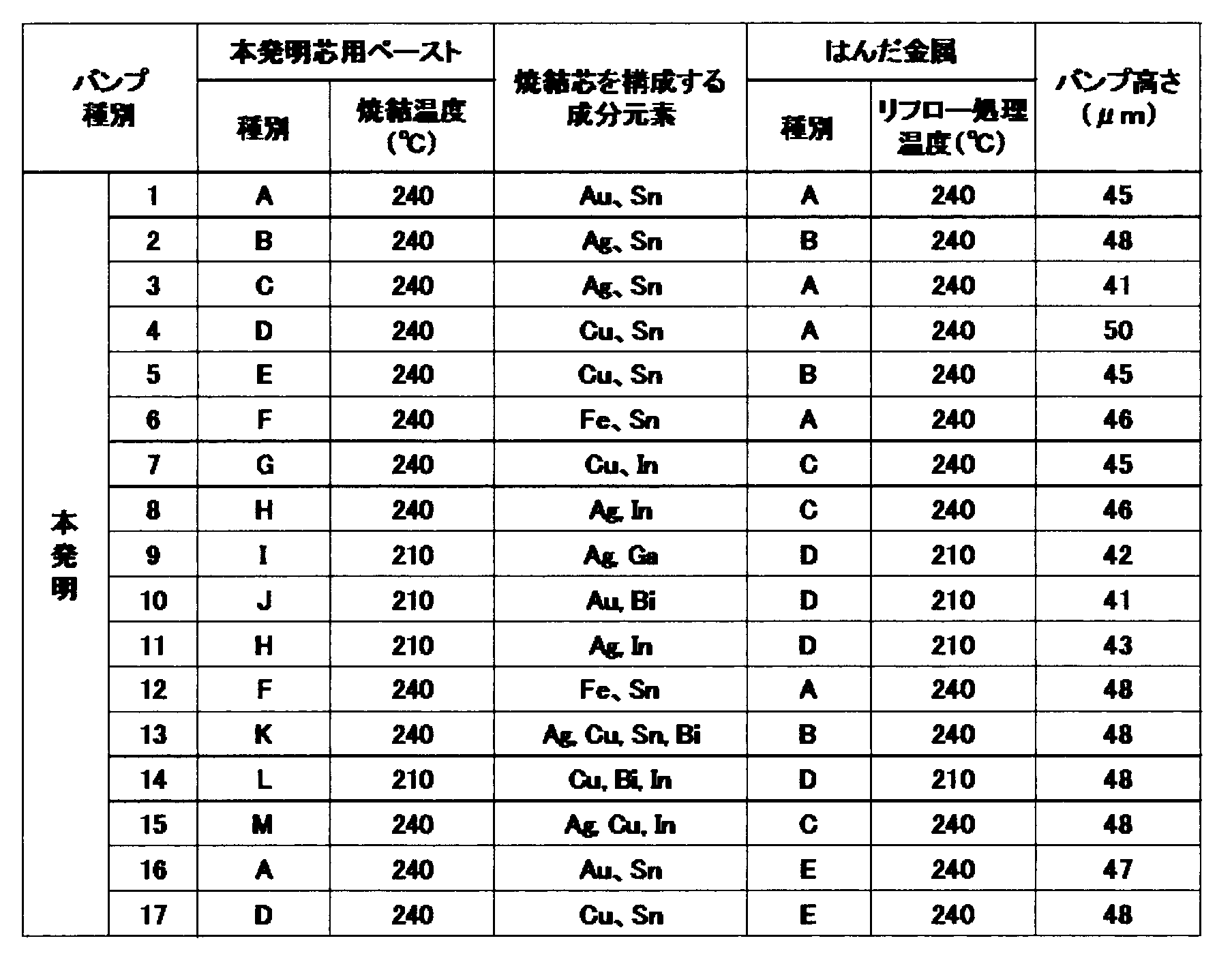
まず、第一工程として、図2(a)~(d)に示すように、パッド電極(直径:85μm)2が形成されている半導体基板1の表面に、パッド電極径より小径の開口(開口直径:43μm、開口ピッチ:150μm)が設けられた厚さ20μmのメタルマスク33を載置し、表2に示す芯用ペースト32(芯用ペーストの種別記号:A~M)をスキージ31によりパッド電極表面に印刷塗布(印刷充填(S1))し、メタルマスク33を取り外した後、印刷塗布した芯用ペースト32を、窒素雰囲気のベルト炉で、表3に示す温度で焼結(S2)して、パッド電極2の中央部にほぼメタルマスク33の厚さに相当する高さを有する焼結芯3を形成する。
次に、第二工程として、図2(e)~(h)に示すように、焼結芯3がほぼ中央部に形成されたパッド電極2の径より大きな開口を有し、焼結芯の高さ以上の厚みを有するメタルマスク35(開口直径:110μm、開口ピッチ:150μm、厚さ:30μm)を載置し、メタルマスク35の開口からパッド電極2の露出部分及び焼結芯全体を覆うようにスキージ36を用いて、表1に示すはんだ金属用粉末を含有するはんだペースト34を印刷塗布(印刷充填(S3))し、メタルマスク35を取り外した後、窒素雰囲気のベルト炉で、はんだペースト34の種類に応じて表3に示す温度でリフロー処理(S4)する。
前記の第一工程及び第二工程により、パッド電極2の表面に、焼結芯をその内部に閉じ込めた表3に示す有芯構造はんだバンプ1~17(以下、「本発明バンプ1~17」という)を作製した。
前記の第一工程及び第二工程により、パッド電極2の表面に、焼結芯をその内部に閉じ込めた表3に示す有芯構造はんだバンプ1~17(以下、「本発明バンプ1~17」という)を作製した。
図4には、焼結芯の一例として、Cu粉およびSn粉の混合物からなる芯用ペーストEを用いて、焼結温度240℃で形成された9個の焼結芯のSEM画像を示す。表3に示す本発明バンプ5の内部には、この焼結芯が閉じ込められて有芯構造のバンプが構成される。(図4中の画像下の文字を削除した事に対応した修正です)
上記で作製した本発明バンプ1~17について、バンプ高さを評価するため、バンプの高さ測定を行った。
測定は、NEXIV VMR-3030(Nikon社製)を使用し、光学式画像解析により、バンプの頂点部から基板までの高さを測定することにより行い、200バンプについての測定値を平均して、バンプ高さとした。なお、本実施例では、パッド電極の直径及びメタルマスクの開口直径が一定であるため、バンプ高さが高いほどアスペスト比は高くなる。
表3に、本発明バンプ1~17について求めたバンプ高さを示す。
測定は、NEXIV VMR-3030(Nikon社製)を使用し、光学式画像解析により、バンプの頂点部から基板までの高さを測定することにより行い、200バンプについての測定値を平均して、バンプ高さとした。なお、本実施例では、パッド電極の直径及びメタルマスクの開口直径が一定であるため、バンプ高さが高いほどアスペスト比は高くなる。
表3に、本発明バンプ1~17について求めたバンプ高さを示す。
[比較例]
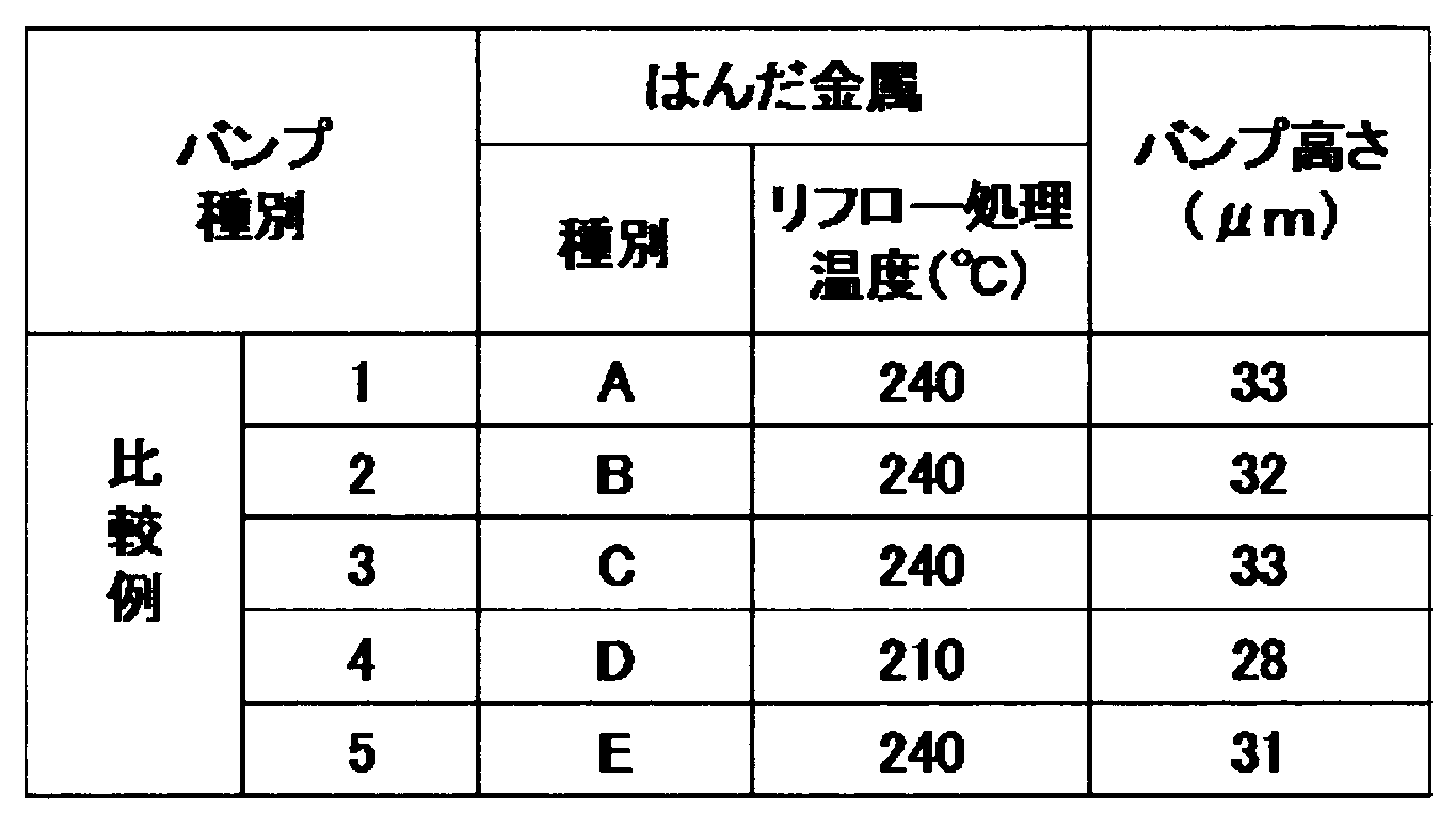
比較のために、パッド電極(直径:85μm)が形成されている半導体基板の表面に、実施例1の第二工程で使用したと同じサイズのメタルマスク(開口直径:110μm、開口ピッチ:150μm、厚さ:30μm)を載置し、メタルマスクの開口からスキージを用いて、表1に示すはんだペーストを印刷塗布し、メタルマスクを取り外した後、窒素雰囲気のベルト炉で、はんだペーストの種類に応じて表4に示す温度でリフロー処理し、パッド電極の表面に、表4に示す比較例のはんだバンプ1~5(以下、「比較例バンプ1~5」という)を作製した。
即ち、比較例バンプ1~5は、芯用ペーストを使用した焼結芯の形成を行っていない点で、本発明バンプ1~17とは、はんだバンプの構造及び製造法が大きく異なっている。
比較のために、パッド電極(直径:85μm)が形成されている半導体基板の表面に、実施例1の第二工程で使用したと同じサイズのメタルマスク(開口直径:110μm、開口ピッチ:150μm、厚さ:30μm)を載置し、メタルマスクの開口からスキージを用いて、表1に示すはんだペーストを印刷塗布し、メタルマスクを取り外した後、窒素雰囲気のベルト炉で、はんだペーストの種類に応じて表4に示す温度でリフロー処理し、パッド電極の表面に、表4に示す比較例のはんだバンプ1~5(以下、「比較例バンプ1~5」という)を作製した。
即ち、比較例バンプ1~5は、芯用ペーストを使用した焼結芯の形成を行っていない点で、本発明バンプ1~17とは、はんだバンプの構造及び製造法が大きく異なっている。
比較例バンプ1~5について、本発明バンプ1~17と同様にして、バンプ高さを求めた。なお、本比較例では、パッド電極の直径及びメタルマスクの開口直径が一定であるため、バンプ高さが高いほどアスペスト比は高くなる。
表4に、比較例バンプ1~5について求めたバンプ高さを示す。
表4に、比較例バンプ1~5について求めたバンプ高さを示す。


[実施例2]
実施例2として、第一群粉末あるいは第二群粉末の少なくとも一方を合金粉末とした表5に示す本発明芯用ペーストN~Rを用いて、実施例1と同様にして、表6に示す有芯構造はんだバンプ18~22(以下、「本発明バンプ18~22」という)を作製した。
なお、このはんだ金属用合金粉末の粒径は、2~12μmであり、平均粒径は、7μmであり、芯用ペーストに含有される金属粉末、合金粉末については、その粒径は1~5μmであり、平均粒径は、2.5μmである。
表6に、本発明バンプ18~22について求めたバンプ高さを示す。
実施例2として、第一群粉末あるいは第二群粉末の少なくとも一方を合金粉末とした表5に示す本発明芯用ペーストN~Rを用いて、実施例1と同様にして、表6に示す有芯構造はんだバンプ18~22(以下、「本発明バンプ18~22」という)を作製した。
なお、このはんだ金属用合金粉末の粒径は、2~12μmであり、平均粒径は、7μmであり、芯用ペーストに含有される金属粉末、合金粉末については、その粒径は1~5μmであり、平均粒径は、2.5μmである。
表6に、本発明バンプ18~22について求めたバンプ高さを示す。
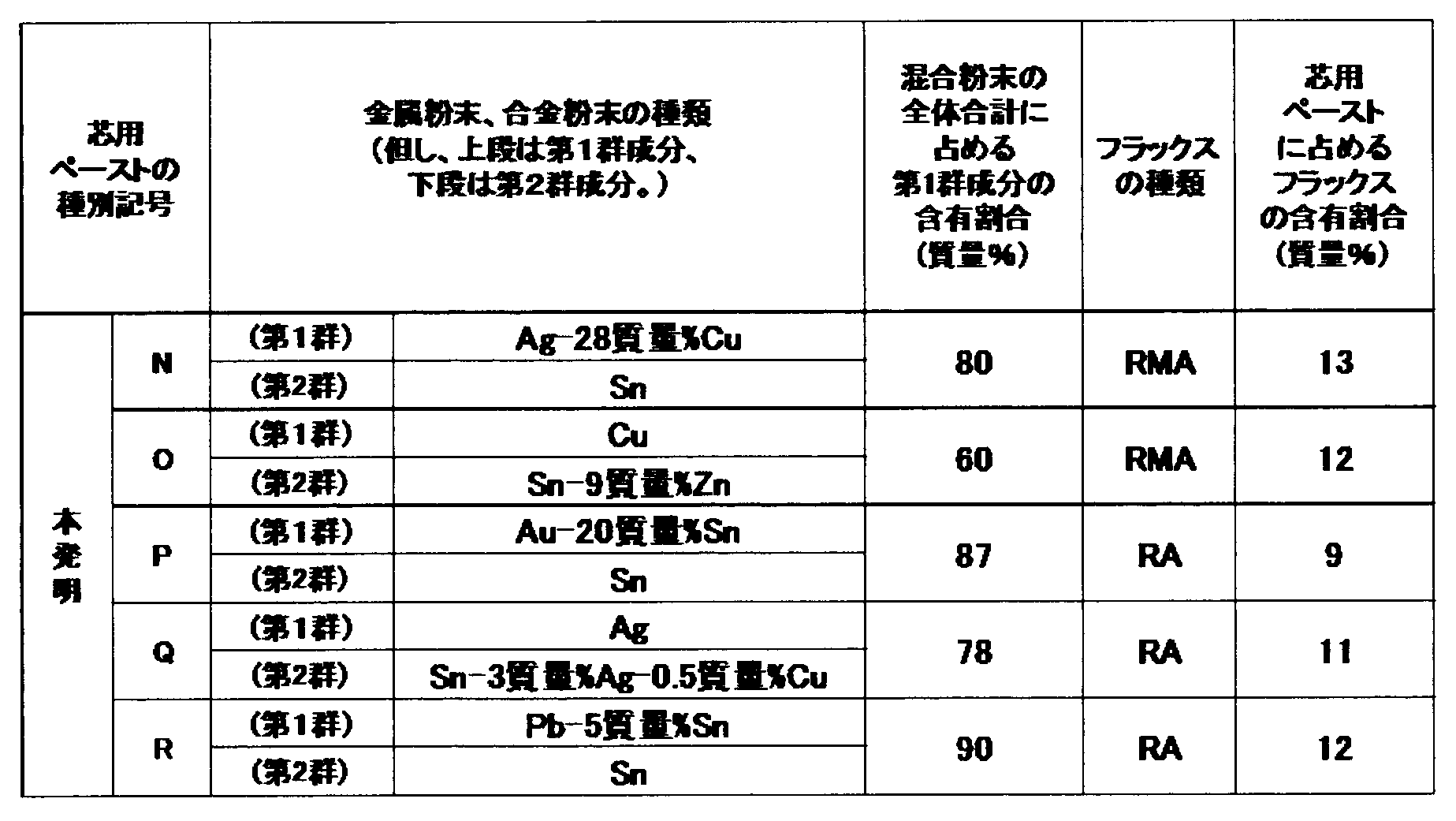
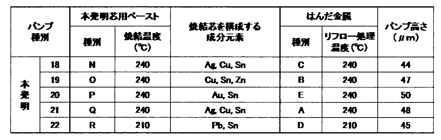
表3、表4、表6に示す結果から、比較例バンプ1~5は、自重による扁平化が生じ、その結果、バンプ高さが30μm前後と低いばかりか、他のバンプとの接触による短絡を引き起こしやすいものであるのに対して、本願発明による有芯構造はんだバンプ1~22は、バンプ高さが40μm以上と高く高アスペクト比を有し、また、バンプ内部に焼結芯が形成されていることによって、焼結芯とはんだ金属との密着性、はんだバンプとパッド電極との密着性がすぐれ、また、導電性を低下させる恐れもないことから、半導体の高密度実装を実現するためのファインピッチ化が可能であることが分かる。
本願発明によりもたらされる有芯構造はんだバンプおよびその製造方法により、半導体の高密度実装化をより低コストで効率良く実現することができるようになる。
1、11 半導体基板
2 パッド電極
3、17 焼結芯
4 はんだ金属
5 高アスペクト比バンプ
12 誘電体層
13 導体パッド
14 バリヤー金属層
15 ピラー金属
16 アンダーバンプ金属層
31、36 スキージ
32 芯用ペースト
33、35 メタルマスク
34 はんだペースト
D バンプ径
H バンプ高さ
S1 印刷充填
S2 焼結
S3 印刷充填
S4 リフロー
2 パッド電極
3、17 焼結芯
4 はんだ金属
5 高アスペクト比バンプ
12 誘電体層
13 導体パッド
14 バリヤー金属層
15 ピラー金属
16 アンダーバンプ金属層
31、36 スキージ
32 芯用ペースト
33、35 メタルマスク
34 はんだペースト
D バンプ径
H バンプ高さ
S1 印刷充填
S2 焼結
S3 印刷充填
S4 リフロー
Claims (4)
- 半導体基板上に形成された有芯構造はんだバンプであって、前記はんだバンプは、はんだバンプの内部に形成され、かつ、半導体基板に垂直な方向に延びる焼結芯と、前記焼結芯の周囲に被着されたはんだ金属との有芯構造からなり、前記焼結芯は、はんだペーストのリフロー処理温度近傍またはそれ以下の温度で焼結された焼結体からなることを特徴とする有芯構造はんだバンプ。
- 前記焼結芯は、第一群粉末と第二群粉末との粉末焼結体、合金焼結体またはこれらの混合焼結体からなり、前記第一群粉末は、第一A群粉末及び第一B群粉末の少なくともいずれかを含有し、前記第一A群粉末は、Cu、Ag、Au、Pt、Pd、Ti、Ni、Fe、Coの内から選ばれた一種又は二種以上の金属粉末からなり、また、前記第一B群粉末は、液相温度が450℃以上のろう合金粉末及び液相温度が280℃以上の高温はんだ合金粉末の内から選ばれた一種又は二種以上の合金粉末からなることを特徴とする請求項1に記載の有芯構造はんだバンプ。
- 前記焼結芯は、第一群粉末と第二群粉末との粉末焼結体、合金焼結体またはこれらの混合焼結体からなり、前記第二群粉末は、第二A群粉末及び第二B群粉末の少なくともいずれかを含有し、前記第二A群粉末は、Sn、In、Bi、Gaの内から選ばれた一種又は二種以上の金属粉末からなり、また、前記第二B群粉末は、液相温度が240℃以下のはんだ合金の合金粉末からなることを特徴とする請求項1に記載の有芯構造はんだバンプ。
- 半導体基板上に形成された有芯構造はんだバンプの製造方法であって、半導体基板上に形成されたパッド電極あるいはアンダーバンプメタルの表面に芯用ペーストを印刷塗布し、はんだペーストのリフロー処理温度近傍またはそれ以下の温度で芯用ペーストを焼結して、パッド電極あるいはアンダーバンプメタルの表面のほぼ中央部分に焼結芯を形成し、次いで、パッド電極あるいはアンダーバンプメタルのほぼ中央部に形成された焼結芯全体を覆うようにはんだペーストを印刷塗布し、はんだペーストのリフロー処理温度でリフロー処理することにより、パッド電極表面上あるいはアンダーバンプメタルの表面上に有芯構造はんだバンプを形成することを特徴とする有芯構造はんだバンプの製造方法。
Priority Applications (2)
| Application Number | Priority Date | Filing Date | Title |
|---|---|---|---|
| CN201480053701.XA CN105593980B (zh) | 2013-12-27 | 2014-12-04 | 有芯结构焊料凸点及其制造方法 |
| KR1020167004857A KR102122631B1 (ko) | 2013-12-27 | 2014-12-04 | 유심 구조 땜납 범프 및 그 제조 방법 |
Applications Claiming Priority (2)
| Application Number | Priority Date | Filing Date | Title |
|---|---|---|---|
| JP2013-270852 | 2013-12-27 | ||
| JP2013270852A JP6226233B2 (ja) | 2013-12-27 | 2013-12-27 | 有芯構造はんだバンプ及びその製造方法 |
Publications (1)
| Publication Number | Publication Date |
|---|---|
| WO2015098460A1 true WO2015098460A1 (ja) | 2015-07-02 |
Family
ID=53478326
Family Applications (1)
| Application Number | Title | Priority Date | Filing Date |
|---|---|---|---|
| PCT/JP2014/082181 Ceased WO2015098460A1 (ja) | 2013-12-27 | 2014-12-04 | 有芯構造はんだバンプ及びその製造方法 |
Country Status (5)
| Country | Link |
|---|---|
| JP (1) | JP6226233B2 (ja) |
| KR (1) | KR102122631B1 (ja) |
| CN (1) | CN105593980B (ja) |
| TW (1) | TWI648835B (ja) |
| WO (1) | WO2015098460A1 (ja) |
Cited By (1)
| Publication number | Priority date | Publication date | Assignee | Title |
|---|---|---|---|---|
| US20210193607A1 (en) * | 2019-12-18 | 2021-06-24 | Micron Technology, Inc. | Processes for forming self-healing solder joints and repair of same, related solder joints, and microelectronic components, assemblies and electronic systems incorporating such solder joints |
Families Citing this family (2)
| Publication number | Priority date | Publication date | Assignee | Title |
|---|---|---|---|---|
| JP6379342B2 (ja) * | 2014-07-09 | 2018-08-29 | 三菱マテリアル株式会社 | 半導体装置及びその製造方法 |
| DE112016006717T5 (de) | 2016-04-06 | 2019-01-03 | Mitsubishi Electric Corporation | Leistungs-halbleitereinheit |
Citations (2)
| Publication number | Priority date | Publication date | Assignee | Title |
|---|---|---|---|---|
| JPH06140532A (ja) * | 1992-10-28 | 1994-05-20 | Ngk Insulators Ltd | バンプ付基板 |
| JP2005294482A (ja) * | 2004-03-31 | 2005-10-20 | Fujikura Ltd | 電子部品及び電子装置 |
Family Cites Families (12)
| Publication number | Priority date | Publication date | Assignee | Title |
|---|---|---|---|---|
| US5466635A (en) * | 1994-06-02 | 1995-11-14 | Lsi Logic Corporation | Process for making an interconnect bump for flip-chip integrated circuit including integral standoff and hourglass shaped solder coating |
| JPH0997791A (ja) * | 1995-09-27 | 1997-04-08 | Internatl Business Mach Corp <Ibm> | バンプ構造、バンプの形成方法、実装接続体 |
| JP3961876B2 (ja) | 2002-05-17 | 2007-08-22 | 株式会社タムラ製作所 | 半導体装置用はんだバンプの製造方法 |
| JP4047065B2 (ja) * | 2002-05-17 | 2008-02-13 | 株式会社タムラ製作所 | 半導体装置用パット電極部の形成方法 |
| US7115998B2 (en) * | 2002-08-29 | 2006-10-03 | Micron Technology, Inc. | Multi-component integrated circuit contacts |
| TWI281718B (en) * | 2002-09-10 | 2007-05-21 | Advanced Semiconductor Eng | Bump and process thereof |
| US6992001B1 (en) * | 2003-05-08 | 2006-01-31 | Kulicke And Soffa Industries, Inc. | Screen print under-bump metalization (UBM) to produce low cost flip chip substrate |
| JP4404063B2 (ja) * | 2006-03-24 | 2010-01-27 | 株式会社村田製作所 | 接続構造、その形成方法、回路基板、および実装基板に表面実装された電子部品 |
| JP2006332694A (ja) | 2006-07-24 | 2006-12-07 | Megic Corp | 半導体表面上に金属バンプを形成する方法 |
| KR101485105B1 (ko) * | 2008-07-15 | 2015-01-23 | 삼성전자주식회사 | 반도체 패키지 |
| JP2013187258A (ja) | 2012-03-06 | 2013-09-19 | Toshiba Corp | 半導体装置および半導体装置の製造方法 |
| JP6156136B2 (ja) * | 2013-12-27 | 2017-07-05 | 三菱マテリアル株式会社 | はんだバンプの焼結芯を形成するための芯用ペースト |
-
2013
- 2013-12-27 JP JP2013270852A patent/JP6226233B2/ja not_active Expired - Fee Related
-
2014
- 2014-12-04 KR KR1020167004857A patent/KR102122631B1/ko active Active
- 2014-12-04 WO PCT/JP2014/082181 patent/WO2015098460A1/ja not_active Ceased
- 2014-12-04 CN CN201480053701.XA patent/CN105593980B/zh active Active
- 2014-12-18 TW TW103144325A patent/TWI648835B/zh active
Patent Citations (2)
| Publication number | Priority date | Publication date | Assignee | Title |
|---|---|---|---|---|
| JPH06140532A (ja) * | 1992-10-28 | 1994-05-20 | Ngk Insulators Ltd | バンプ付基板 |
| JP2005294482A (ja) * | 2004-03-31 | 2005-10-20 | Fujikura Ltd | 電子部品及び電子装置 |
Cited By (2)
| Publication number | Priority date | Publication date | Assignee | Title |
|---|---|---|---|---|
| US20210193607A1 (en) * | 2019-12-18 | 2021-06-24 | Micron Technology, Inc. | Processes for forming self-healing solder joints and repair of same, related solder joints, and microelectronic components, assemblies and electronic systems incorporating such solder joints |
| US11646286B2 (en) * | 2019-12-18 | 2023-05-09 | Micron Technology, Inc. | Processes for forming self-healing solder joints and repair of same, related solder joints, and microelectronic components, assemblies and electronic systems incorporating such solder joints |
Also Published As
| Publication number | Publication date |
|---|---|
| KR20160102150A (ko) | 2016-08-29 |
| TW201541594A (zh) | 2015-11-01 |
| TWI648835B (zh) | 2019-01-21 |
| JP2015126158A (ja) | 2015-07-06 |
| KR102122631B1 (ko) | 2020-06-12 |
| JP6226233B2 (ja) | 2017-11-08 |
| CN105593980B (zh) | 2019-03-19 |
| CN105593980A (zh) | 2016-05-18 |
Similar Documents
| Publication | Publication Date | Title |
|---|---|---|
| JP4753090B2 (ja) | はんだペースト、及び電子装置 | |
| TWI586811B (zh) | Lead - free solder bump joint construction | |
| JP5533665B2 (ja) | 電子装置の製造方法、電子部品搭載用基板及びその製造方法 | |
| JP6476823B2 (ja) | ピラー形成用ペースト、ピラーの製造方法、バンプ構造体の製造方法、ピラー、及びバンプ構造体 | |
| JP6004253B2 (ja) | ペースト用はんだ合金粉末、ペースト及びこれを用いたはんだバンプ | |
| JP6226233B2 (ja) | 有芯構造はんだバンプ及びその製造方法 | |
| KR101983510B1 (ko) | 핵재료 및 납땜 이음 및 범프 전극의 형성 방법 | |
| JP6350967B2 (ja) | 半導体装置及びその製造方法 | |
| JP6156136B2 (ja) | はんだバンプの焼結芯を形成するための芯用ペースト | |
| US8252677B2 (en) | Method of forming solder bumps on substrates | |
| JP6379342B2 (ja) | 半導体装置及びその製造方法 | |
| JP2006165336A (ja) | バンプ形成用ハンダペースト | |
| JP5147349B2 (ja) | バンプ形成用ペースト、及びバンプ構造体 | |
| TWI479967B (zh) | Solder precoating method | |
| WO2015008789A1 (ja) | はんだバンプ製造方法 | |
| JP2013237088A (ja) | バンプ用はんだ合金粉末、ペースト及びこれを用いたはんだバンプ | |
| JP2013237090A (ja) | バンプ用はんだ合金粉末、ペースト及びこれを用いたはんだバンプ | |
| KR102389258B1 (ko) | 고온 안정성과 필렛특성이 개선된 접합 페이스트 및 그의 제조방법 | |
| JP2009200285A (ja) | バンプ及びバンプ接続構造体 | |
| JP2015003323A (ja) | ニードル低減はんだ合金粉末、ペースト及びこれを用いたはんだバンプ | |
| JP2015000428A (ja) | ニードル低減はんだ合金粉末、ペースト及びこれを用いたはんだバンプ |
Legal Events
| Date | Code | Title | Description |
|---|---|---|---|
| 121 | Ep: the epo has been informed by wipo that ep was designated in this application |
Ref document number: 14875419 Country of ref document: EP Kind code of ref document: A1 |
|
| ENP | Entry into the national phase |
Ref document number: 20167004857 Country of ref document: KR Kind code of ref document: A |
|
| NENP | Non-entry into the national phase |
Ref country code: DE |
|
| 122 | Ep: pct application non-entry in european phase |
Ref document number: 14875419 Country of ref document: EP Kind code of ref document: A1 |