WO2015075985A1 - 半導体装置およびその書き込み方法 - Google Patents
半導体装置およびその書き込み方法 Download PDFInfo
- Publication number
- WO2015075985A1 WO2015075985A1 PCT/JP2014/072293 JP2014072293W WO2015075985A1 WO 2015075985 A1 WO2015075985 A1 WO 2015075985A1 JP 2014072293 W JP2014072293 W JP 2014072293W WO 2015075985 A1 WO2015075985 A1 WO 2015075985A1
- Authority
- WO
- WIPO (PCT)
- Prior art keywords
- memory transistor
- active layer
- transistor
- gate
- memory
- Prior art date
- Legal status (The legal status is an assumption and is not a legal conclusion. Google has not performed a legal analysis and makes no representation as to the accuracy of the status listed.)
- Ceased
Links
Images










Classifications
-
- G—PHYSICS
- G11—INFORMATION STORAGE
- G11C—STATIC STORES
- G11C17/00—Read-only memories programmable only once; Semi-permanent stores, e.g. manually-replaceable information cards
- G11C17/14—Read-only memories programmable only once; Semi-permanent stores, e.g. manually-replaceable information cards in which contents are determined by selectively establishing, breaking or modifying connecting links by permanently altering the state of coupling elements, e.g. PROM
- G11C17/18—Auxiliary circuits, e.g. for writing into memory
-
- G—PHYSICS
- G11—INFORMATION STORAGE
- G11C—STATIC STORES
- G11C13/00—Digital stores characterised by the use of storage elements not covered by groups G11C11/00, G11C23/00, or G11C25/00
- G11C13/0002—Digital stores characterised by the use of storage elements not covered by groups G11C11/00, G11C23/00, or G11C25/00 using resistive RAM [RRAM] elements
- G11C13/0007—Digital stores characterised by the use of storage elements not covered by groups G11C11/00, G11C23/00, or G11C25/00 using resistive RAM [RRAM] elements comprising metal oxide memory material, e.g. perovskites
-
- G—PHYSICS
- G11—INFORMATION STORAGE
- G11C—STATIC STORES
- G11C13/00—Digital stores characterised by the use of storage elements not covered by groups G11C11/00, G11C23/00, or G11C25/00
- G11C13/0002—Digital stores characterised by the use of storage elements not covered by groups G11C11/00, G11C23/00, or G11C25/00 using resistive RAM [RRAM] elements
- G11C13/0021—Auxiliary circuits
- G11C13/0069—Writing or programming circuits or methods
-
- G—PHYSICS
- G11—INFORMATION STORAGE
- G11C—STATIC STORES
- G11C17/00—Read-only memories programmable only once; Semi-permanent stores, e.g. manually-replaceable information cards
- G11C17/14—Read-only memories programmable only once; Semi-permanent stores, e.g. manually-replaceable information cards in which contents are determined by selectively establishing, breaking or modifying connecting links by permanently altering the state of coupling elements, e.g. PROM
- G11C17/16—Read-only memories programmable only once; Semi-permanent stores, e.g. manually-replaceable information cards in which contents are determined by selectively establishing, breaking or modifying connecting links by permanently altering the state of coupling elements, e.g. PROM using electrically-fusible links
-
- G—PHYSICS
- G11—INFORMATION STORAGE
- G11C—STATIC STORES
- G11C17/00—Read-only memories programmable only once; Semi-permanent stores, e.g. manually-replaceable information cards
- G11C17/14—Read-only memories programmable only once; Semi-permanent stores, e.g. manually-replaceable information cards in which contents are determined by selectively establishing, breaking or modifying connecting links by permanently altering the state of coupling elements, e.g. PROM
- G11C17/16—Read-only memories programmable only once; Semi-permanent stores, e.g. manually-replaceable information cards in which contents are determined by selectively establishing, breaking or modifying connecting links by permanently altering the state of coupling elements, e.g. PROM using electrically-fusible links
- G11C17/165—Memory cells which are electrically programmed to cause a change in resistance, e.g. to permit multiple resistance steps to be programmed rather than conduct to or from non-conduct change of fuses and antifuses
-
- G—PHYSICS
- G11—INFORMATION STORAGE
- G11C—STATIC STORES
- G11C19/00—Digital stores in which the information is moved stepwise, e.g. shift registers
- G11C19/28—Digital stores in which the information is moved stepwise, e.g. shift registers using semiconductor elements
-
- H—ELECTRICITY
- H10—SEMICONDUCTOR DEVICES; ELECTRIC SOLID-STATE DEVICES NOT OTHERWISE PROVIDED FOR
- H10B—ELECTRONIC MEMORY DEVICES
- H10B20/00—Read-only memory [ROM] devices
- H10B20/20—Programmable ROM [PROM] devices comprising field-effect components
-
- H—ELECTRICITY
- H10—SEMICONDUCTOR DEVICES; ELECTRIC SOLID-STATE DEVICES NOT OTHERWISE PROVIDED FOR
- H10D—INORGANIC ELECTRIC SEMICONDUCTOR DEVICES
- H10D30/00—Field-effect transistors [FET]
- H10D30/60—Insulated-gate field-effect transistors [IGFET]
- H10D30/67—Thin-film transistors [TFT]
- H10D30/674—Thin-film transistors [TFT] characterised by the active materials
- H10D30/6755—Oxide semiconductors, e.g. zinc oxide, copper aluminium oxide or cadmium stannate
-
- H—ELECTRICITY
- H10—SEMICONDUCTOR DEVICES; ELECTRIC SOLID-STATE DEVICES NOT OTHERWISE PROVIDED FOR
- H10D—INORGANIC ELECTRIC SEMICONDUCTOR DEVICES
- H10D30/00—Field-effect transistors [FET]
- H10D30/60—Insulated-gate field-effect transistors [IGFET]
- H10D30/67—Thin-film transistors [TFT]
- H10D30/6757—Thin-film transistors [TFT] characterised by the structure of the channel, e.g. transverse or longitudinal shape or doping profile
-
- H—ELECTRICITY
- H10—SEMICONDUCTOR DEVICES; ELECTRIC SOLID-STATE DEVICES NOT OTHERWISE PROVIDED FOR
- H10D—INORGANIC ELECTRIC SEMICONDUCTOR DEVICES
- H10D62/00—Semiconductor bodies, or regions thereof, of devices having potential barriers
- H10D62/80—Semiconductor bodies, or regions thereof, of devices having potential barriers characterised by the materials
-
- G—PHYSICS
- G02—OPTICS
- G02F—OPTICAL DEVICES OR ARRANGEMENTS FOR THE CONTROL OF LIGHT BY MODIFICATION OF THE OPTICAL PROPERTIES OF THE MEDIA OF THE ELEMENTS INVOLVED THEREIN; NON-LINEAR OPTICS; FREQUENCY-CHANGING OF LIGHT; OPTICAL LOGIC ELEMENTS; OPTICAL ANALOGUE/DIGITAL CONVERTERS
- G02F1/00—Devices or arrangements for the control of the intensity, colour, phase, polarisation or direction of light arriving from an independent light source, e.g. switching, gating or modulating; Non-linear optics
- G02F1/01—Devices or arrangements for the control of the intensity, colour, phase, polarisation or direction of light arriving from an independent light source, e.g. switching, gating or modulating; Non-linear optics for the control of the intensity, phase, polarisation or colour
- G02F1/13—Devices or arrangements for the control of the intensity, colour, phase, polarisation or direction of light arriving from an independent light source, e.g. switching, gating or modulating; Non-linear optics for the control of the intensity, phase, polarisation or colour based on liquid crystals, e.g. single liquid crystal display cells
- G02F1/133—Constructional arrangements; Operation of liquid crystal cells; Circuit arrangements
- G02F1/1333—Constructional arrangements; Manufacturing methods
- G02F1/1345—Conductors connecting electrodes to cell terminals
- G02F1/13452—Conductors connecting driver circuitry and terminals of panels
-
- G—PHYSICS
- G02—OPTICS
- G02F—OPTICAL DEVICES OR ARRANGEMENTS FOR THE CONTROL OF LIGHT BY MODIFICATION OF THE OPTICAL PROPERTIES OF THE MEDIA OF THE ELEMENTS INVOLVED THEREIN; NON-LINEAR OPTICS; FREQUENCY-CHANGING OF LIGHT; OPTICAL LOGIC ELEMENTS; OPTICAL ANALOGUE/DIGITAL CONVERTERS
- G02F1/00—Devices or arrangements for the control of the intensity, colour, phase, polarisation or direction of light arriving from an independent light source, e.g. switching, gating or modulating; Non-linear optics
- G02F1/01—Devices or arrangements for the control of the intensity, colour, phase, polarisation or direction of light arriving from an independent light source, e.g. switching, gating or modulating; Non-linear optics for the control of the intensity, phase, polarisation or colour
- G02F1/13—Devices or arrangements for the control of the intensity, colour, phase, polarisation or direction of light arriving from an independent light source, e.g. switching, gating or modulating; Non-linear optics for the control of the intensity, phase, polarisation or colour based on liquid crystals, e.g. single liquid crystal display cells
- G02F1/133—Constructional arrangements; Operation of liquid crystal cells; Circuit arrangements
- G02F1/136—Liquid crystal cells structurally associated with a semi-conducting layer or substrate, e.g. cells forming part of an integrated circuit
- G02F1/1362—Active matrix addressed cells
- G02F1/1368—Active matrix addressed cells in which the switching element is a three-electrode device
-
- G—PHYSICS
- G02—OPTICS
- G02F—OPTICAL DEVICES OR ARRANGEMENTS FOR THE CONTROL OF LIGHT BY MODIFICATION OF THE OPTICAL PROPERTIES OF THE MEDIA OF THE ELEMENTS INVOLVED THEREIN; NON-LINEAR OPTICS; FREQUENCY-CHANGING OF LIGHT; OPTICAL LOGIC ELEMENTS; OPTICAL ANALOGUE/DIGITAL CONVERTERS
- G02F2201/00—Constructional arrangements not provided for in groups G02F1/00 - G02F7/00
- G02F2201/12—Constructional arrangements not provided for in groups G02F1/00 - G02F7/00 electrode
- G02F2201/123—Constructional arrangements not provided for in groups G02F1/00 - G02F7/00 electrode pixel
-
- G—PHYSICS
- G11—INFORMATION STORAGE
- G11C—STATIC STORES
- G11C2213/00—Indexing scheme relating to G11C13/00 for features not covered by this group
- G11C2213/50—Resistive cell structure aspects
- G11C2213/53—Structure wherein the resistive material being in a transistor, e.g. gate
Definitions
- the present invention relates to a semiconductor device including a memory transistor.
- memory transistor an element having a transistor structure (hereinafter referred to as “memory transistor”) as a memory element that can be used as a ROM (read only memory).
- Patent Document 1 discloses a nonvolatile memory transistor having a MOS transistor structure. In this memory transistor, writing is performed by applying a high electric field to the gate insulating film to cause dielectric breakdown.
- Patent Document 2 discloses a memory transistor using a change in threshold voltage caused by applying a predetermined write voltage to the gate.
- Patent Document 3 by the present applicant proposes a novel nonvolatile memory transistor capable of reducing power consumption as compared with the prior art.
- This memory transistor uses a metal oxide semiconductor in an active layer (channel), and can irreversibly change to a resistor state showing ohmic resistance characteristics regardless of the gate voltage due to Joule heat generated by a drain current.
- the voltage for writing can be made lower than the voltage in Patent Documents 1 and 2. Note that in this specification, the operation of changing the metal oxide semiconductor of the memory transistor to the resistor state is referred to as “writing”.
- reading an operation of reading a current flowing between the drain and the source from the memory transistor is referred to as “reading”, and a current read from the memory transistor is referred to as “reading current”.
- This memory transistor does not operate as a transistor because a metal oxide semiconductor becomes a resistor after writing.
- the memory transistor is also referred to as a “memory transistor” even after being changed to a resistor.
- names of a gate electrode, a source electrode, a drain electrode, an active layer, a channel region, and the like constituting a transistor structure are used.
- Patent Document 3 describes that a memory transistor is formed on, for example, an active matrix substrate of a liquid crystal display device.
- An object of the embodiment of the present invention is to increase the read operation margin of the sense amplifier by suppressing the decrease in the read current from the memory transistor, thereby ensuring the reliability of the semiconductor device.
- a semiconductor device includes at least one memory cell and a write control circuit that controls writing to the at least one memory cell, wherein the at least one memory cell includes an active metal oxide.
- the memory transistor irreversibly from a semiconductor state in which the drain current Ids depends on the gate-source voltage Vgs to a resistor state in which the drain current Ids does not depend on the gate-source voltage Vgs.
- the write control circuit is configured to satisfy Vgs ⁇ Vds + Vth when the threshold voltage of the memory transistor is Vth and the drain-source voltage of the memory transistor is Vds.
- Drain electrode, source By controlling the voltage applied to the electrode and the gate electrode, and is configured to perform writing to the memory transistor.
- the at least one memory cell is a plurality of memory cells
- the plurality of memory cells include a memory cell including the memory transistor S in the semiconductor state and a memory transistor R in the resistor state. Including a memory cell.
- the metal oxide includes a first metal element
- the active layer of the memory transistor R includes more of the first metal element in a metal state than the active layer of the memory transistor S. Including.
- the first metal element in the metal state is present more on the drain side than on the source side in the channel region in the active layer.
- the memory transistor includes a gate electrode, the active layer, a first insulating layer disposed between the gate electrode and the active layer, and a side opposite to the first insulating layer. And the second insulating layer is in contact with the surface of the active layer, and the first metal element in the metal state is in contact with the active layer and the second insulating layer. Present at the interface with the layer.
- the first metal element in the metal state is present in the active layer.
- the metal oxide includes at least In, and the first metal element in the metal state is In.
- the active layer of the memory transistor R includes more voids than the active layer of the memory transistor S.
- the active layer of the memory transistor R includes a void existing in the vicinity of the drain electrode.
- the composition of the metal oxide differs between the channel region in the active layer of the memory transistor R and the channel region in the active layer of the memory transistor S.
- the active layer includes a first metal element and a second metal element, and the first metal element has a higher standard electrode potential than the second metal element, and the memory transistor R
- the content of the second metal element in the ionic state with respect to the entire metal element in the ionic state included in the active layer of the active layer of the memory transistor S is the ionic state relative to the entire metal element in the ionic state included in the active layer of the memory transistor S. It is larger than the content rate of the second metal element.
- the active layer includes a first metal element and a second metal element, and the first metal element has a higher standard electrode potential than the second metal element, and the memory transistor R
- the content of the first metal element in the ionic state relative to the entire metal element in the ionic state included in the active layer of the active layer of the memory transistor S is the ionic state relative to the entire metal element in the ionic state included in the active layer of the memory transistor S. It is smaller than the content rate of the first metal element.
- the metal oxide includes at least In and Ga, the first metal element is In, and the second metal element is Ga.
- the metal oxide includes In, Ga, and Zn.
- the metal oxide includes a crystalline portion.
- no organic insulating film is formed above the active layer of the memory transistor.
- the electronic device includes any one of the semiconductor devices described above.
- a writing method is a writing method of a semiconductor device including a memory cell, wherein the memory cell includes a memory transistor having an active layer including a metal oxide, and the memory transistor includes a drain current.
- the drain current Ids can be irreversibly changed from a semiconductor state in which Ids depends on the gate-source voltage Vgs to a resistor state in which the drain current Ids does not depend on the gate-source voltage Vgs.
- the present invention since writing is performed on the memory transistor in the linear region of the memory transistor, uniform Joule heat is generated between the drain and source of the memory transistor, and the composition of the metal oxide is between the drain and source. Change uniformly. As a result, the decrease in the read current is suppressed, the read operation margin of the sense amplifier can be increased, and the reliability of the semiconductor device can be ensured.
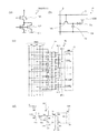
- FIG. 4A is a diagram illustrating a single memory cell constituting the memory circuit 3001 in the first embodiment
- FIG. 4B is a block diagram illustrating the configuration of the memory circuit 3001.
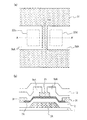
- FIG. 4A is a plan view of an active matrix substrate 1002 according to the first embodiment
- FIG. 4A is a plan view of an active matrix substrate 1002 according to the first embodiment
- FIG. 4B is a cross-sectional view illustrating a display device 2001 using the active matrix substrate 1002.
- 2 is a diagram illustrating a block configuration of a liquid crystal display device 2001.
- FIG. FIGS. 4A to 4D are schematic views showing configurations of memory cells constituting the nonvolatile memory devices 60a to 60c, a pixel circuit of the liquid crystal display device 2001, a gate driver 76, and one stage of the gate driver 76, respectively.
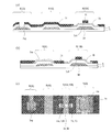
- It is. 4A and 4B are process diagrams for explaining a manufacturing method of the semiconductor device (active matrix substrate 1002) according to the first embodiment, in which FIGS. 4A and 4B are cross-sectional views and FIG.
- FIGS. 4A and 4B are process diagrams for explaining a manufacturing method of the semiconductor device (active matrix substrate 1002) according to the first embodiment, in which FIGS. 4A and 4B are cross-sectional views and FIG. 4A and 4B are process diagrams for explaining a manufacturing method of the semiconductor device (active matrix substrate 1002) according to the first embodiment, in which FIGS. 4A and 4B are cross-sectional views and FIG. 4A and 4B are process diagrams for explaining a manufacturing method of the semiconductor device (active matrix substrate 1002) according to the first embodiment, in which FIGS. 4A and 4B are cross-sectional views and FIG.
- FIG. 1A and 1B are a circuit block diagram illustrating a semiconductor device (integrated circuit) 2002 according to the first embodiment and a cross-sectional view illustrating a part of the semiconductor device.
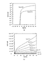
- (A) is a diagram showing Ids-Vgs characteristics in the initial state (semiconductor state) of the memory transistor 10A
- (b) is a diagram showing Ids-Vds characteristics in the initial state of the memory transistor 10A.
- (A) is a figure which shows the Ids-Vgs characteristic in the resistor body state of the memory transistor 10A
- (b) is a figure which shows the Ids-Vds characteristic in the resistor body state of the memory transistor 10A.
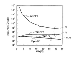
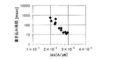
- FIG. 10 is a diagram showing the Ids-Vgs characteristics of the memory transistor 10A before and after writing in an overlapping manner. It is a figure which shows the relationship between the differential resistance (dVds / dIds, unit: ohm micrometer) of the memory transistor 10A before and behind writing, and the drain voltage Vds. It is a figure which shows an example of the relationship between the writing time (unit: m second) of memory transistor 10A, and unit drain current (unit: A / micrometer).
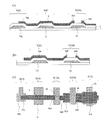
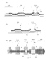
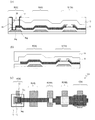
- FIG. 4 is a process diagram for explaining a method for manufacturing a semiconductor device (active matrix substrate 1003) of a second embodiment, wherein (a) and (b) are sectional views, and (c) are top views.
- FIG. 4 is a process diagram for explaining a method for manufacturing a semiconductor device (active matrix substrate 1003) of a second embodiment, wherein (a) and (b) are sectional views, and (c) are top views.
- FIG. 4 is a process diagram for explaining a method for manufacturing a semiconductor device (active matrix substrate 1003) of a second embodiment, wherein (a) and (b) are sectional views, and (c) are top views.
- FIG. 4 is a process diagram for explaining a method for manufacturing a semiconductor device (active matrix substrate 1003) of a second embodiment, wherein (a) and (b) are sectional views, and (c) are top views.
- FIG. 4 is a process diagram for explaining a method for manufacturing a semiconductor device (active matrix substrate 1003) of a second embodiment, wherein (a) and (b) are sectional views, and (c) are top views.
- (A) And (b) is the top view and sectional drawing which show 10 A of memory transistors in the semiconductor device of 3rd Embodiment, respectively.
- FIG. 4 is a process diagram for explaining a method for manufacturing a semiconductor device (active matrix substrate 1003) of a second embodiment, wherein (a) and (b) are sectional views, and (c) are top views.
- (A) And (b) is the top view and sectional drawing which show 10 A of memory transistors in the semiconductor device of 3rd Embodiment, respectively.
- FIG. 4 is a process diagram for explaining a method for manufacturing a semiconductor device (active matrix substrate 1004) of a third embodiment, wherein (a) and (b) are cross-sectional views, and (c) are top views.
- FIG. 4 is a process diagram for explaining a method for manufacturing a semiconductor device (active matrix substrate 1004) of a third embodiment, wherein (a) and (b) are cross-sectional views, and (c) are top views.
- FIG. 4 is a process diagram for explaining a method for manufacturing a semiconductor device (active matrix substrate 1004) of a third embodiment, wherein (a) and (b) are cross-sectional views, and (c) are top views.
- (A) And (b) is the top view and sectional drawing which illustrate the structure of the other memory transistor in embodiment by this invention.
- (A)-(c) is sectional drawing which illustrates the structure of the other semiconductor device in embodiment by this invention. It is a figure which shows typically the state of the metal oxide of the memory transistor after writing in a linear area
- the present inventor has repeatedly studied the condition of the write voltage for suppressing the decrease in the read current from the memory transistor in the semiconductor device including the memory transistor disclosed in Patent Document 3. Specifically, the inventor examined the relationship between the gate-source voltage Vgs of the memory transistor, the drain-source voltage Vds, the threshold voltage Vth of the memory transistor, and the read current at the time of writing.
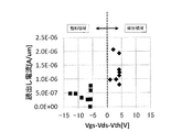
- FIG. 1 shows the relationship between the write voltage Vds, the gate voltage Vgs, the threshold voltage Vth of the memory transistor, and the read current.
- the horizontal axis indicates the voltage value obtained from Vgs ⁇ Vds ⁇ Vth, and the vertical axis indicates the value of read current per unit channel width (A / ⁇ m).
- the “linear region” and the “nonlinear region” can be confirmed in the electrical characteristics of a general transistor (the relationship between the drain-source voltage Vds and the drain current Ids).
- the “linear region” is a region where the drain current Ids changes according to the change of the drain-source voltage Vds, and the “saturation region” is the drain without depending on the change of the drain-source voltage Vds. This is a region where the current Ids is substantially constant.
- Vds it is known that a region satisfying Vds ⁇ Vgs ⁇ Vth is a linear region, and a region satisfying Vds> Vgs ⁇ Vth is a saturation region.
- a linear region and a saturated region are distinguished from each other with Vgs-Vth as a boundary depending on the magnitude relationship between Vds and Vgs-Vth. Therefore, in FIG. 1, a region where Vgs ⁇ Vds ⁇ Vth ⁇ 0 represents a linear region, and a region where Vgs ⁇ Vds ⁇ Vth ⁇ 0 represents a saturated region.
- the drain-source voltage Vds at the time of writing is set to 20 to 30 V, and after writing in the linear region, the drain-source voltage Vds is set to 10 V and the gate-source voltage at the time of reading.
- the result of measuring the read current with Vgs set to ⁇ 10 V is plotted with “ ⁇ ”.
- the drain-source voltage Vds at the time of writing is set to 20 to 30 V, and after writing in the saturation region, the drain-source voltage Vds is set to 10 V and the gate-source voltage Vgs is set at the time of reading.
- the result of measuring the read current with -10V set is plotted with " ⁇ ".
- the voltage Vds at the time of reading is not limited to 10V, and the voltage Vgs is not limited to -10V. From the viewpoint of low power consumption, it is preferable that the voltages Vds and Vgs are small. For example, the voltage Vds can be set to 0.1V.
- the present inventor has found the condition of the write voltage that can suppress the decrease in the read current from the memory transistor, and has reached the present invention.
- a first embodiment of a semiconductor device includes a first thin film transistor and a second thin film transistor on the same substrate.
- the first thin film transistor is a memory transistor that functions as a memory element.
- the second thin film transistor is a transistor that does not function as a memory element and forms a circuit. In this specification, such a transistor is referred to as a “circuit transistor” and is distinguished from a memory transistor.
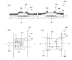
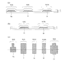
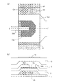
- FIG. 2A is a cross-sectional view showing a memory transistor (first thin film transistor) 10A and a circuit transistor (second thin film transistor) 10B in the semiconductor device 1001 of this embodiment.
- 2B and 2C are plan views of the memory transistor 10A and the circuit transistor 10B, respectively.
- FIG. 2A shows a cross-sectional structure taken along line I-I ′ in FIG. 2B and line II-II ′ in FIG.
- the semiconductor device 1001 includes a substrate 1, a memory transistor 10 ⁇ / b> A supported on the substrate 1, and a circuit transistor 10 ⁇ / b> B supported on the substrate 1.
- the circuit transistor 10B may be any circuit element that constitutes a circuit, and its application is not limited. Further, these transistors 10A and 10B may have active layers (oxide semiconductor layers) 7A and 7B containing a common metal oxide.
- the memory transistor 10A can be irreversibly changed from a state where the drain current Ids depends on the gate voltage Vgs (referred to as a semiconductor state) to a state where the drain current Ids does not depend on the gate voltage Vgs (referred to as a resistor state). It is a non-volatile memory element.
- the drain current Ids is a current flowing between the drain and the source of the memory transistor 10A, and the gate voltage Vgs is a voltage between the gate and the source.
- the above state change occurs, for example, when a predetermined write voltage Vds is applied between the drain and source of the memory transistor 10A in the semiconductor state (initial state).
- Vds write voltage
- a current flows through a portion (channel region) 7cA where the channel is formed in the active layer 7A, and Joule heat is generated.
- This Joule heat reduces the resistance of the channel region 7cA in the active layer 7A.
- a resistor state having an ohmic resistance characteristic is obtained without depending on the gate voltage Vgs.
- the semiconductor device 1001 may include a plurality of memory transistors 10A.
- writing is performed in a linear region.
- the plurality of memory transistors 10A after the writing include, for example, a memory transistor S in a semiconductor state and a memory transistor R in a resistor state.
- the memory transistor R is a write target, and the memory transistor S is not a write target.
- composition of metal oxide> As a result of analyzing the composition in the metal oxide of the memory transistor before and after writing, the present inventor confirmed that the metal oxide of the memory transistor was changed by writing. Hereinafter, an example of the analysis result will be described.
- a memory transistor including a metal oxide containing In (indium), Ga (gallium), and Zn (zinc) was used. Mainly, the composition (before and after writing) of the metal oxide near the center of the channel region was analyzed.
- the composition analysis of the metal oxide can be performed using, for example, Auger electron spectroscopy.
- the “content ratio” of the metal element in this specification is defined.
- the “content ratio” of a metal element means the ratio of each metal element in an ionic state to the entire metal element in an ionic state contained in the active layer. In the sample used for analysis, before writing, it was confirmed that the In content was 0.29, the Ga content was 0.33, and the Zn content was 0.37 near the center of the channel region. It was.
- the In content is 0.10
- the Ga content is 0.54
- the Zn content is 0.35 near the center of the channel region. It was confirmed. Thereby, the content of In in the ionic state of the active layer after writing is smaller than the content of In in the ionic state of the active layer before writing, and the content of Ga in the ionic state of the active layer after writing is It was found that the ionic state Ga content of the active layer before writing increased.
- the present inventor has examined the analysis results and obtained the following knowledge.
- the obtained knowledge will be described with reference to FIG.
- FIG. 30 schematically shows the state of the metal oxide of the memory transistor after writing in the linear region.
- the active layer in the memory transistor R contains more In in the metal state than the active layer in the memory transistor S. The reason for this is currently being elucidated, but it is considered that the bond between In and oxygen was weakened by Joule heat, and part of the oxygen bonded to In diffused outside the channel region.
- the active layer in the memory transistor R contains more voids than the active layer in the memory transistor S.
- the active layer in the memory transistor R includes a void that exists in the vicinity of the drain electrode. This is considered to be caused by precipitation of metal In and oxygen deficiency.
- composition of the metal oxide differs between the channel region in the active layer of the memory transistor R and the channel region in the active layer of the memory transistor S. The reason for this is considered that Joule heat and electromigration occurred in the channel region.
- the ionic state Ga content in the active layer of the memory transistor R is larger than the ionic state Ga content in the active layer of the memory transistor S.
- the content of In in the ionic state in the active layer of the memory transistor R is smaller than the content of In in the ionic state in the active layer of the memory transistor S.
- the reason for this is considered to be that the bond between In and oxygen is weakened by Joule heat, and a part of In is precipitated as In in a metallic state.
- the reason why the read current from the memory transistor increases when writing in the linear region is that the metal layer In is deposited in the entire active layer, particularly in the entire channel region. This is thought to be due to the decrease in electrical resistivity.
- the active layer of the memory transistor R contains Ga in an ionic state. It is considered that the rate is the largest and the content of In in the ionic state is the smallest (Ga> Zn> In).
- the above shows an analysis result of the composition of the metal oxide which is a ternary oxide of In, Ga, Zn as an example.
- the metal oxide is, for example, a ternary oxide of In, Ga, Sn. Similar analysis results can be obtained in some cases or in the case of a binary oxide of In and Zn.
- the metal oxide contains two or more kinds of metal elements, it is considered that the metal element having the higher standard electrode potential is likely to precipitate as a metal in the metal oxide.
- the lower the standard electrode potential the more easily the metal element is ionized and oxidized.
- the active layer includes the first metal element and the second metal element, and the first metal element has a higher standard electrode potential than the second metal element, the first metal element It is easier to change from an ionic state to a metal state than the second metal element.
- the active layer of the memory transistor R may contain more first metal element in the metal state than the active layer of the memory transistor S.
- the first metal element in the metal state is present more on the drain side than on the source side in the channel region, and may also be present at the interface between the active layer and the second insulating layer (protective film) and inside the active layer. .
- the content ratio of the second metal element in the ionic state in the active layer of the memory transistor R is larger than the content ratio of the second metal element in the ionic state in the active layer of the memory transistor S.
- the content ratio of the first metal element in the ionic state in the active layer may be smaller than the content ratio of the first metal element in the ionic state in the active layer of the memory transistor S.
- the memory transistor 10A includes an active layer 7A including an oxide semiconductor, a gate electrode 3A, a gate insulating film 5 disposed between the active layer 7A and the gate electrode 3A, and the gate insulating film 5 and the active layer 7A. Another insulating film (not shown) in contact with the surface of the active layer 7A located on the opposite side of the interface, a source electrode 9sA disposed so as to contact a part of the active layer 7A, and another one of the active layer 7A A drain electrode 9dA arranged so as to be in contact with the portion.
- the active layer 7 ⁇ / b> A When viewed from the normal direction of the substrate 1, at least a part of the active layer 7 ⁇ / b> A is disposed so as to overlap the gate electrode 3 ⁇ / b> A through the gate insulating film 5.
- the active layer 7A, the source electrode 9sA, and the drain electrode 9dA need only be electrically connected, and may not be in direct contact.
- a region in contact with the source electrode 9sA (or a region electrically connected) is a “source contact region”
- a region in contact with the drain electrode 9dA (or a region electrically connected) is a “drain contact region”. Called.
- a region overlapping the gate electrode 3A and the gate insulating film 5 and located between the source contact region and the drain contact region in the active layer 7A is the channel region 7cA. Become.
- the entire active layer 7A overlaps the gate electrode 3A, and the active layer 7A is in direct contact with the source electrode 9sA and the drain electrode 9dA.
- the channel length of the memory transistor 10A corresponds to the length of the gap portion between the source electrode 9sA and the drain electrode 9dA on the active layer 7A in the channel direction when viewed from the normal direction of the substrate 1.
- the channel width corresponds to the length of the gap portion in the direction orthogonal to the channel direction.
- the drain electrode 9dA when viewed from the normal direction of the substrate 1, one of the drain electrode 9dA and the source electrode 9sA (here, the drain electrode 9dA) has a recess on the active layer 7A.
- the other electrode here, the source electrode 9sA
- the channel region 7cA located between the source electrode 9sA and the drain electrode 9dA has a U shape.
- the width of the gap portion positioned between the source electrode 9sA and the drain electrode 9dA is the channel length.
- the length of a line in the channel region 7cA in which the distance from the source electrode 9sA and the distance from the drain electrode 9dA are equal to each other (divided into two equal parts of the separation distance on the active layer 7A between the source electrode 9sA and the drain electrode 9dA).
- the length of the line connecting the points) is the channel width.
- the circuit transistor 10B includes an active layer 7B, a gate electrode 3B, a gate insulating film 5 positioned between the active layer 7B and the gate electrode 3B, and a source electrode disposed in contact with a part of the active layer 7B. 9 sB, and a drain electrode 9 dB disposed so as to be in contact with another part of the active layer 7A.
- the active layer 7B may include an oxide semiconductor common to the active layer 7A.
- the gate electrode 3B is disposed so as to overlap at least a part of the active layer 7B.
- the active layer 7B has a source contact region in contact with (or electrically connected to) the source electrode 9sB, and a drain contact region in contact with (or electrically connected to) the drain electrode 9dB. And a channel region 7cB.
- the channel region 7cB overlaps with the gate electrode 3B via the gate insulating film 5 when viewed from the normal direction of the substrate 1 and is located between the source contact region and the drain contact region in the active layer 7B. It is.
- the channel length of the circuit transistor 10B is the length in the channel direction of the gap portion between the source electrode 9sB and the drain electrode 9dB on the active layer 7B, and the channel width is the direction orthogonal to the channel direction of the gap portion. Is the length of
- the gate electrodes 3A and 3B of the memory transistor 10A and the circuit transistor 10B are formed from a common gate conductive film.
- the gate insulating film 5 of the memory transistor 10 ⁇ / b> A extends to the circuit transistor 10 ⁇ / b> B and functions as a gate insulating film of the circuit transistor 10.
- the source electrodes 9sA and 9sB and the drain electrodes 9dA and 9dB of the memory transistor 10A and the circuit transistor 10B are formed from a common source conductive film.
- the circuit transistor 10B and the memory transistor 10A can be formed using a common process, so that the number of manufacturing steps can be reduced.
- the planar shape of the channel region 7cA of the memory transistor 10A is U-shaped, but may be rectangular.
- the planar shape of the channel region 7cB of the circuit transistor 10B is rectangular, but may be U-shaped.
- the channel region is U-shaped, it is considered that the Joule heat generated by the write current can be used more efficiently for reducing the resistance (writing) of the channel region.
- the memory transistor 10A and the circuit transistor 10B are not limited to the bottom gate structure, and may have a top gate structure. However, if the memory transistor 10A and the circuit transistor 10B have the same structure, these transistors 10A and 10B can be formed using a common process.
- the oxide semiconductor film to be the active layers 7A and 7B of the memory transistor 10A and the circuit transistor 10B is, for example, an In—Ga—Zn—O based semiconductor film.
- a TFT having an In—Ga—Zn—O-based semiconductor layer has high mobility (more than 20 times that of an a-Si TFT) and low leakage current (less than 1/100 of that of an a-Si TFT).
- a TFT having an In—Ga—Zn—O-based semiconductor layer is used, power consumption of the display device can be significantly reduced.
- the In—Ga—Zn—O based semiconductor may be amorphous or may contain a crystalline part.
- a crystalline In—Ga—Zn—O-based semiconductor in which the c-axis is oriented substantially perpendicular to the layer surface may be used.
- Such a crystal structure of an In—Ga—Zn—O-based semiconductor is disclosed in, for example, Japanese Patent Laid-Open No. 2012-134475. For reference, the entire disclosure of Japanese Patent Application Laid-Open No. 2012-134475 is incorporated herein by reference.
- oxide semiconductor film instead of the In—Ga—Zn—O-based semiconductor, another semiconductor film capable of reducing resistance due to Joule heat may be used.
- a semiconductor film containing NiO, SnO 2 , TiO 2 , VO 2 , In 2 O 3 , or SrTiO 3 may be used.
- Zn—O based semiconductor ZnO
- In—Zn—O based semiconductor IZO (registered trademark)
- Zn—Ti—O based semiconductor ZTO
- Cd—Ge—O based semiconductor Cd—Pb—O Semiconductors such as CdO (cadmium oxide), Mg—Zn—O semiconductors, In—Sn—Zn—O semiconductors (eg, In 2 O 3 —SnO 2 —ZnO), In—Ga—Sn—O semiconductors, etc. It can also be used. Further, films obtained by adding various impurities to these oxide semiconductors may be used.
- the memory transistor 10A can be used in a memory circuit that stores information in a nonvolatile manner, for example, by assigning a semiconductor state (initial state) to a logical value “0” and a resistor state to a logical value “1”. .
- a semiconductor state initial state
- a resistor state to a logical value “1”.
- FIG. 3A is a diagram illustrating a single memory cell constituting the memory circuit.
- the memory cell includes, for example, a memory transistor 10A and a memory cell selection transistor (referred to as a “selection transistor”) 10D connected in series to the memory transistor 10A. ing.
- the selection transistor 10D may have an active layer formed of the same oxide semiconductor film as the active layer of the memory transistor 10A. Thereby, the memory transistor 10A and the selection transistor 10D can be easily manufactured using a common process.
- the circuit transistor 10B shown in FIG. 2 includes a selection transistor 10D.
- a write or read operation to the memory transistor 10A is enabled by applying a gate voltage to the selection transistor 10D to turn it on.
- Writing to the memory transistor 10A is performed in a linear region for a period (writing time) Tpp. Specifically, the voltage is applied to the drain electrode, the source electrode, and the gate electrode of the memory transistor so that Vgs ⁇ Vds + Vth is satisfied. During this time, the source electrode of the selection transistor 10D is connected to a fixed voltage (for example, GND). Thereby, the write current Ipp flows through the channel region of the memory transistor 10A during the period Tpp. By the write current Ipp, uniform Joule heat is generated between the drain and the source, and the composition of the oxide semiconductor can be changed uniformly between the drain and the source. As a result, the channel region is in a resistor state in which the resistance is reduced. Needless to say, the source electrode of the selection transistor 10D only needs to be fixed to the reference voltage Vss.
- Reading of the memory transistor 10A can be performed by examining the gate voltage dependence of the current (read current) flowing by applying a predetermined voltage between the drain and source of the memory transistor 10A. Specifically, when it is assumed that the read current flowing through the memory transistor 10A in the semiconductor state is It, it can be easily determined by the ratio of the read current Ir at the time of reading to the current It. When the gate voltage Vgs at the time of reading is set within a predetermined voltage range (for example, about 0.5 V or less), the difference between the reading current It and the reading current Ir is large, so that the state of the memory transistor 10A can be made easier. Can be determined.
- a predetermined voltage range for example, about 0.5 V or less
- FIG. 3B shows a configuration example of the memory circuit 3001 in which a plurality of memory cells are arranged in the row direction and the column direction.
- a plurality of memory cells are arranged in the row direction and the column direction. Note that the plurality of memory cells may be arranged only in the row direction, or may be arranged only in the column direction.
- the memory circuit 3001 typically includes a plurality of memory cells, a first plurality of word lines PL, a second plurality of word lines WL, a plurality of bit lines BL, a word line decoder 104, and a sense.
- An amplifier circuit 106 and a write control circuit 107 are provided.
- the memory cell includes one memory transistor and two selection transistors. k memory cells are arranged in the column direction, and l memory cells are arranged in the row direction. That is, a plurality of memory cells are arranged in a k ⁇ l matrix.
- the memory cell may be composed of one memory transistor and one selection transistor, as shown in FIG. Alternatively, a configuration in which three or more selection transistors are connected in parallel to each other and each selection transistor is connected in series with the memory transistor may be employed. However, by connecting a plurality of selection transistors in parallel to each other, it is possible to suppress a decrease in the current driving capability of the selection transistors.
- the gate electrode of the memory transistor 10A in the memory cells arranged in the same row is connected to the write control circuit 107 via the word line PLn corresponding to each row. Further, the gate electrodes of the two selection transistors in the memory cells arranged in the same row are connected to the word line decoder 104 via the word line WLn corresponding to each row.
- the drain electrode of the memory transistor 10A in the memory cells arranged in the same column is connected to the write control circuit 107 and the sense amplifier circuit 106 via the bit line BLn corresponding to each column.
- the source electrode of each select transistor in the memory cell is connected to a reference voltage line (not shown). As described above, in the present embodiment, the reference voltage is a GND level voltage.
- the write control circuit 107 includes a bit line voltage control circuit 102, a bit line decoder 103, and a write voltage control circuit 105.
- the write control circuit 107 controls writing to the memory cell.
- the bit line voltage control circuit 102 generates a write voltage Vpp (Vds) necessary for writing so as to satisfy Vgs ⁇ Vds + Vth, and supplies the generated voltage Vpp to the bit line decoder 103. Further, the bit line voltage control circuit 102 generates a read drain voltage Vdr necessary for reading, and supplies the generated voltage to the bit line decoder 103.
- the bit line decoder 103 decodes an address input from the outside, and selects one or a plurality of bit lines BL connected to one or a plurality of memory cells to be written or read.
- the bit line decoder 103 applies the write voltage Vpp or the read drain voltage Vdr to the selected bit line BLn, and applies the non-selected bit line voltage (for example, the reference voltage Vss) to the unselected bit line BLn.
- the word line decoder 104 decodes an address inputted from the outside and selects one or more word lines WL connected to one or more memory cells to be written. In addition, one word line WL connected to one or a plurality of memory cells to be read is selected. The word line decoder 104 controls each word line WL so as to turn on the selection transistor in the selected memory cell and turn off the selection transistor in the memory cell that is not selected. Specifically, the word line decoder 104 applies a high level gate voltage (for example, a write voltage Vpp) that turns on the selection transistor to the word line WLn connected to the selected memory cell. Further, the word line decoder 104 applies a low level voltage VL at which the selection transistor is turned off to the remaining unselected word lines WLn.
- a high level gate voltage for example, a write voltage Vpp
- the write voltage control circuit 105 decodes an address input from the outside and selects one or more word lines PLn connected to one or more memory cells to be written. At the time of writing, the write voltage control circuit 105 generates a write gate voltage Vgs so as to satisfy Vgs ⁇ Vds + Vth, and applies the generated gate voltage Vgs to the selected word line PLn. The write voltage control circuit 105 applies a low level voltage VL to the non-selected word line PLn.
- the write voltage control circuit 105 applies a low level voltage VL (for example, the read drain voltage Vdr) that does not turn on the memory transistor 10A to all the word lines PLn at the time of reading.
- VL for example, the read drain voltage Vdr
- the bit line voltage control circuit 102 and the write voltage control circuit 105 are electrically connected within the write control circuit 107, and information indicating the voltages Vds and Vgs between the bit line voltage control circuit 102 and the write voltage control circuit 105. Are sent and received. Thereby, the bit line voltage control circuit 102 generates the voltage Vds based on the information on the voltage Vgs from the write voltage control circuit 105 so as to satisfy Vgs ⁇ Vds + Vth. The write voltage control circuit 105 generates the voltage Vgs based on the information on the voltage Vds from the bit line voltage control circuit 102 so that Vgs ⁇ Vds + Vth is satisfied.
- the sense amplifier circuit 106 typically includes the same number of sense amplifiers as the total number l of the bit lines BL.
- the sense amplifier circuit 106 detects a read current Ir flowing from the selected bit line BLn to the memory cell to be read via the bit line decoder 103. Then, it is determined whether the state of the memory transistor 10A in the memory cell to be read is a semiconductor state (initial state) or a resistor state.
- the sense amplifier included in the sense amplifier circuit 106 is typically a current sense type that detects the read current Ir, but may be a voltage sense type that detects a node voltage on the read current path. . Further, instead of a circuit configuration connected to the bit line decoder 103 via the bit line BLn, a circuit configuration in which the sense amplifier circuit 106 is connected to a reference voltage line VSL provided independently for each column is adopted. May be.
- the write control circuit 107 and the word line decoder 104 are configured as independent circuits, but the embodiment of the present invention is not limited to this.
- the write control circuit 107 and the word line decoder 104 may be configured by one integrated circuit for controlling the bit line and the word line. In such a case, one integrated circuit can be a write control circuit.
- the plurality of memory cells arranged in the row direction and the column direction include a memory cell including the memory transistor S in a semiconductor state and a memory transistor R in a resistor state. Including the memory cell.
- the bit line voltage control circuit 102 At the time of writing, the bit line voltage control circuit 102 generates a write voltage Vpp (Vds) necessary at the time of writing so as to satisfy Vgs ⁇ Vds + Vth.
- the bit line decoder 103 applies the generated write voltage Vpp to the selected bit line BLn.
- the write voltage control circuit 105 generates a voltage Vgs necessary for writing so as to satisfy Vgs ⁇ Vds + Vth, and applies the generated voltage Vgs to the selected word line PLn.
- Word line decoder 104 applies a voltage having the same level as write voltage Vpp to selected word line WLn.
- the unselected bit line BLn is in a floating state (high impedance state), and a low level voltage VL is applied to the unselected word lines PLn and WLn. Note that a voltage of the same level as the write voltage Vpp may be applied to the unselected word line PLn.
- the write operation to the memory transistor 10A is performed in the memory cell to be written in accordance with the write operation to the memory transistor 10A described above.
- the bit line decoder 103 applies a voltage necessary for reading to the selected bit line BLn, and the word line decoder 104 applies a high level voltage to the selected word line WLn.
- the write voltage control circuit 105 applies a low level voltage VL that does not turn on the memory transistors to all the word lines PLn.
- the memory transistor 10A in the memory cell to be read When the memory transistor 10A in the memory cell to be read is in the resistor state, the memory transistor 10A has conductivity. Therefore, even if a low level voltage VL is applied to the word line PLn, the bit line BLn Thus, a current flows through the memory transistor 10A.
- the memory transistor 10A in the memory cell to be read is in the semiconductor state, that is, in the initial state, when the low level voltage VL is applied to the word line PLn, the memory transistor 10A is turned off, and the bit line No current flows through the memory transistor 10A via BLn.
- the memory state of each memory cell can be detected by detecting the difference in read current (ratio of read current) by the sense amplifier.
- the present embodiment can be widely applied to electronic devices including a memory circuit.
- the semiconductor device of the present embodiment is not limited as long as it includes at least one memory transistor 10A.
- it may be a non-volatile semiconductor memory device, an integrated circuit (IC, LSI), various display devices such as a liquid crystal display device and an organic EL display device, and an active matrix substrate used for various display devices.
- IC integrated circuit
- LSI integrated circuit
- various display devices such as a liquid crystal display device and an organic EL display device
- an active matrix substrate used for various display devices.
- a memory circuit including a memory transistor 10A may be provided in a region (peripheral region) other than the display region of the active matrix substrate.
- the circuit transistor 10B may be a circuit transistor that forms a peripheral circuit such as a drive circuit provided in the peripheral region.
- a plurality of thin film transistors having an active layer including an oxide semiconductor common to the active layer of the memory transistor 10A may be formed as a circuit element.
- This embodiment can be applied to, for example, an active matrix substrate used in a liquid crystal display device.
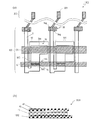
- FIG. 4A is a plan view showing a part of the active matrix substrate 1002.
- the active matrix substrate 1002 includes a display area 100 including a plurality of pixels 101 and an area (peripheral area) 200 other than the display area.
- a thin film transistor (referred to as “pixel transistor”) 10C is formed as a switching element.
- pixel transistor a thin film transistor
- at least a part of a plurality of circuits (a memory circuit, a drive circuit, etc.) constituting the display device is formed monolithically in the peripheral region 200.
- a circuit formed in the peripheral region 200 is referred to as a “peripheral circuit”.
- the memory transistor 10A is used in a memory circuit formed in the peripheral region 200, for example.
- the circuit transistor 10B is a thin film transistor that constitutes any peripheral circuit, for example, a drive circuit.
- the circuit transistor 10B may be a pixel transistor 10C provided in each pixel.
- Each pixel 101 is provided with a source wiring S extending along the pixel column direction, a gate wiring G extending along the pixel row direction, and a pixel electrode 19.
- the pixel transistor 10C is disposed in the vicinity of the point where the source line S and the gate line G intersect.
- the pixel 101 is provided with a capacitor wiring CS formed of the same conductive film as the gate wiring G.
- a capacitor unit 20 is disposed on the capacitor wiring CS.
- the peripheral region 200 is provided with a plurality of terminal portions 201 for connecting the gate wiring G or the source wiring S to the external wiring.
- the source line S extends to the end of the display region 100 and is connected to the source connection portion 9sg.
- the source connection portion 9sg is electrically connected to the gate connection portion 3sg formed of the same film as the gate wiring G. This connection portion is referred to as a “source / gate connection portion” 30.
- the gate connection portion 3sg extends to the peripheral region 200 and is connected to, for example, a source driver (not shown) via a terminal portion (source terminal) 201.
- the gate line G also extends to the peripheral region 200 and is connected to, for example, a gate driver (not shown) via a terminal portion (gate terminal).
- a plurality of peripheral circuits including a memory circuit are formed monolithically.
- a driving circuit such as a gate driver or a source driver and a memory circuit connected to each driving circuit may be formed.
- the memory circuit includes a memory transistor 10A shown in FIG. 2, and the memory circuit or other peripheral circuit includes a circuit transistor 10B shown in FIG.
- the memory transistor 10A and the circuit transistor 10B formed in the peripheral region 200 and the pixel transistor 10C formed in the display region 100 have an active layer formed of a common oxide semiconductor film. Also good. In this case, these transistors 10A to 10C can be manufactured using a common process.
- the active matrix substrate 1002 can be applied to a display device such as a liquid crystal display device.
- the liquid crystal display device includes an active matrix substrate 1002, a counter substrate 41 having a counter electrode 42 on the surface, and a liquid crystal layer 43 disposed therebetween.
- a voltage is applied to the liquid crystal layer 43 for each pixel by the pixel electrode 19 and the counter electrode 42, whereby display is performed.
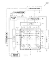
- FIG. 5 is a diagram illustrating a block configuration of a liquid crystal display device 2001 using the active matrix substrate 1002.
- 6A to 6D show the configuration of one stage of the memory cells constituting the nonvolatile memory devices 60a to 60c, the pixel circuit of the liquid crystal display device 2001, the gate driver 76, and the gate driver 76, respectively.
- FIG. 5 is a diagram illustrating a block configuration of a liquid crystal display device 2001 using the active matrix substrate 1002.
- 6A to 6D show the configuration of one stage of the memory cells constituting the nonvolatile memory devices 60a to 60c, the pixel circuit of the liquid crystal display device 2001, the gate driver 76, and the gate driver 76, respectively.
- FIG. 1 is a diagram illustrating a block configuration of a liquid crystal display device 2001 using the active matrix substrate 1002.
- the liquid crystal display device 2001 includes a display unit 71 including a plurality of pixels.
- the display unit 71 corresponds to the display region 100 (FIG. 4A) of the active matrix substrate 1002.
- the display unit 71 has a plurality of pixel circuits 70 arranged in a matrix. These pixel circuits 70 are connected to each other by source lines SL1 to SLk, gate lines GL1 to GLj, and auxiliary capacitance lines CSL1 to CSLj.
- Each pixel circuit 70 includes a pixel transistor 10C, a liquid crystal capacitor Clc, and an auxiliary capacitor Cs, as shown in FIG. 6B.
- the source electrode of the pixel transistor 10C is connected to the source line S
- the gate electrode is connected to the gate line G
- the drain electrode is connected to the pixel electrode (not shown).
- a liquid crystal capacitor Clc is formed by the pixel electrode and the common electrode COM
- an auxiliary capacitor Cs is formed by the pixel electrode and the capacitor wiring CS.
- the liquid crystal display device 2001 also includes a source driver 75 electrically connected to the source line S, a gate driver 76 electrically connected to the gate line G, a CS driver 77 electrically connected to the capacitor line CS, A common electrode drive circuit 74 for driving the common electrode is provided.
- These drive circuits 75, 76, 77, 74 supply power to the display control circuit 73 that controls timing and voltages applied to the source wiring S, gate wiring G, capacitance wiring CS, and common electrode, and these circuits. It is connected to a power supply circuit (not shown).
- the source driver 75, the gate driver 76, and the display control circuit 73 are connected to the nonvolatile storage devices 60a, 60b, and 60c, respectively.
- the nonvolatile storage devices 60a, 60b, and 60c are connected to the common memory control circuit unit 61.
- Nonvolatile memory devices 60a, 60b, and 60c have, for example, a configuration in which a plurality of memory cells are arranged in an array.
- the memory cell includes a memory transistor 10A.
- the memory cell may have the configuration described above with reference to FIG. Alternatively, as illustrated in FIG. 6A, two or more selection transistors 10D and 10E connected in parallel may be provided instead of the selection transistor 10D illustrated in FIG.
- the nonvolatile storage device 60a stores display panel configuration information, a unique ID, and the like.
- Information stored in the nonvolatile storage device 60a is referred to by the display control circuit 73, and detailed display control methods are switched or control parameters are optimized based on the information.
- the unique ID or the like can be inquired from the system side connected to the display panel, and is used for discrimination of the display panel, selection of an optimum driving method, and the like.
- the display control circuit 73 switches a circuit used for display control based on information stored in the nonvolatile storage device 60a, and realizes optimal display control of the display.
- the nonvolatile storage device 60b stores information on configuration parameters necessary for driving the gate driver, such as redundant relief information for the gate driver.
- the nonvolatile memory device 60c stores information on configuration parameters necessary for driving the source driver, such as redundant relief information for the source driver.
- FIG. 4A shows a monolithic structure.
- the gate driver 76 is monolithically formed on the active matrix substrate.
- the gate driver 76 includes a shift register 410 having a plurality of stages as shown in FIG.
- i-stage bistable circuits are provided so as to correspond to the respective rows of the pixel matrix on a one-to-one basis.
- the bistable circuit included in the shift register 410 includes ten thin film transistors MA, MB, MI, MF, MJ, MK, ME, ML, MN, and MD, and a capacitor CAP1 are provided.
- the bistable circuit also has an input terminal for receiving the first clock CKA, an input terminal for receiving the second clock CKB, an input terminal for receiving the third clock CKC, an input terminal for receiving the fourth clock CKD, and an input for receiving the set signal S.
- the plurality of thin film transistors included in the bistable circuit illustrated in FIG. 6D and the memory transistor 10A included in any of the nonvolatile memory devices 60a to 60c are shared by the common oxide semiconductor film.
- An active layer formed from At least one, preferably all, of the thin film transistors included in the bistable circuit corresponds to the circuit transistor 10B shown in FIG.
- the channel length (or channel length / channel width) of the memory transistor 10A is the channel length (or channel length / channel width) of the plurality of thin film transistors and the pixel transistor 10C included in the bistable circuit shown in FIG. Or less, preferably less than the minimum value.
- the gate driver 76 has been described here as an example, the same applies to the case where other circuits including a thin film transistor are formed monolithically.
- Detailed circuit configurations of the display control circuit 73, the common electrode drive circuit 74, the source driver 75, and the CS driver 77 are substantially the same as the configuration of a known liquid crystal display device, and thus detailed description thereof is omitted.
- At least one of the thin film transistors constituting the monolithically formed circuit may correspond to the circuit transistor 10B described above with reference to FIG.
- the active matrix substrate 1002 all the thin film transistors functioning as circuit elements in all the circuits (circuits connected to the same power supply circuit) in the same power supply domain region as the circuit including the memory transistor 10A This corresponds to the transistor 10B.
- the pixel transistor 10C may be the circuit transistor 10B. Note that part of the circuit may be formed over another substrate attached to the active matrix substrate 1002.
- FIGS. 7 to 10 are process diagrams for explaining the manufacturing method of the active matrix substrate 1002, in which (a) and (b) are cross-sectional views, and (c) is a top view.
- a region R (10A) for forming the memory transistor 10A a region R (10B) for forming the circuit transistor 10B, a region R (20) for forming the capacitor portion 20, gate / source A region R (30) for forming the contact portion 30 and a region R (40) for forming the gate / source intersection 40 are shown.
- the gate-source intersection 40 includes a gate wiring or a conductive layer formed from the same conductive film as the gate wiring and a conductive layer formed from the same conductive film as the source wiring or the source wiring through an insulating layer. Refers to the intersection.
- the formation regions of the transistors 10A and 10B, the capacitor portion 20, and the like are shown side by side, but the arrangement of these formation regions is not limited to the arrangement shown.
- a conductive film for a gate is formed on the substrate 1 by, for example, a sputtering method, and is patterned by a well-known dry etching method.
- the gate connection portion 3sg is formed in the gate / source contact portion formation region R (30)
- the gate wiring is formed in the gate / source intersection formation region R (40).
- a gate electrode 3A is formed in the memory transistor formation region R (10A)
- a capacitor wiring CS is formed in the capacitor portion formation region R (20)
- a gate electrode 3B is formed in the circuit transistor formation region R (10B).
- a layer including these wirings and electrodes formed from the gate conductive film is referred to as a “gate wiring layer”.
- a transparent insulating substrate such as a glass substrate
- a conductive film for a gate for example, a single layer film such as aluminum (Al), chromium (Cr), copper (Cu), tantalum (Ta), titanium (Ti), molybdenum (Mo), or tungsten (W), A laminated film in which two or more layers are laminated, or an alloy film containing two or more elements among the above metal elements may be used.
- a three-layer film (Ti / Al / Ti) having a Ti film, an Al film and a Ti film in this order from the substrate 1 side, a three-layer film (Mo / Ti) having a Mo film, an Al film and a Mo film in this order. / Mo) or the like can be used.
- a gate insulating film 5 is formed so as to cover the gate wiring layer.
- the gate insulating film 5 is formed by, for example, a plasma CVD method or a sputtering method.
- Examples of the gate insulating film 5 include a silicon oxide film (SiO 2 ), a silicon nitride film (SiN), a silicon oxynitride film (SiNO), a silicon nitride oxide film (SiON), aluminum oxide (Al 2 O 3 ), and an oxide.
- a single layer selected from tantalum (Ta 2 O 5 ) or a laminated film of two or more layers may be used.
- a two-layer film having an SiN film having a thickness of 100 to 500 nm and an SiO 2 film having a thickness of 20 to 100 nm in this order from the substrate 1 side is used.
- the oxide semiconductor film is patterned by a well-known wet etching method.
- the active layer 7A is formed in the memory transistor formation region R (10A)
- the active layer 7B is formed in the circuit transistor formation region R (10B).
- the active layers 7A and 7B are arranged so as to overlap the corresponding gate electrodes 3A and 3B with the gate insulating film 5 interposed therebetween, respectively.
- the width of the gate electrodes 3A and 3B in the channel direction is made substantially equal, and the width of the active layer 7A in the channel direction is made smaller than the width of the active layer 7B in the channel direction.
- the width of the active layer 7A in the channel direction is smaller than the width of the gate electrode 3A in the channel direction
- the width of the active layer 7B in the channel direction is larger than the width of the gate electrode 3B in the channel direction.
- an oxide semiconductor film containing In, Ga, and Zn can be used.
- an In—Ga—Zn—O-based amorphous oxide semiconductor film (thickness :, for example, 20 to 200 nm) is used.
- This semiconductor film is an n-type metal oxide semiconductor and is formed at a low temperature.
- the composition ratio In: Ga: Zn of each metal element in the In—Ga—Zn—O-based oxide semiconductor film is, for example, 1: 1: 1. Even if the composition ratio is adjusted on the basis of this composition ratio, the effect of the present invention is obtained.
- a source conductive film is formed on the gate insulating film 5 and the active layers 7A and 7B by, for example, a sputtering method, and the source conductive film is patterned by a well-known dry etching method.
- the source connection portion 9sg is formed in the gate / source contact portion formation region R (30) and the source wiring is formed in the gate / source intersection formation region R (40).
- the source electrode 9sA and the drain electrode 9dA in the memory transistor formation region R (10A), the capacitance electrode 9cs in the capacitance portion formation region R (20), and the source electrode 9sB and the drain electrode 9dB in the circuit transistor formation region R (10B). Form each one.
- a layer including these wirings and electrodes formed from the source conductive film is referred to as a “source wiring layer”.
- the source electrode 9sA and the drain electrode 9dA are electrically separated from each other and are in contact with a part of the active layer 7A. Be placed.
- the source electrode 9sB and the drain electrode 9dB are disposed so as to be electrically separated from each other and in contact with a part of the active layer 7B.
- regions overlapping the corresponding gate electrodes 3A and 3B and located between the source electrodes 9sA and 7sB and the drain electrodes 9dA and 7dB are channel regions 7cA and 7cB.
- the source electrode 9sA and the drain electrode 9dA are arranged so that the channel region 7cA is U-shaped when viewed from the normal direction of the substrate 1.
- the source electrode 9sB and the drain electrode 9dB are arranged so that the channel region 7cB is rectangular when viewed from the normal direction of the substrate 1. In this way, the memory transistor 10A and the circuit transistor 10B are formed.
- the capacitor portion 20 having the capacitor wiring CS, the capacitor electrode 9cs, and the dielectric layer (here, the gate insulating film 5) positioned therebetween is formed.
- the gate / source intersection forming region R (40) a gate / source intersection 40 is formed at which the gate line G and the source line S intersect via the gate insulating film 5.
- the source connection part 9sg is arranged so as to overlap a part of the gate connection part 3sg with the gate insulating film 5 interposed therebetween.
- a single layer film such as aluminum (Al), chromium (Cr), copper (Cu), tantalum (Ta), titanium (Ti), molybdenum (Mo), or tungsten (W),
- a laminated film in which two or more layers are laminated, or an alloy film containing two or more elements among the above metal elements may be used.
- a three-layer film (Ti / Al / Ti) having a Ti film, an Al film and a Ti film in this order from the substrate 1 side a three-layer film (Mo / Ti) having a Mo film, an Al film and a Mo film in this order. / Mo) or the like can be used.
- a protective film (passivation film) 11 is formed so as to cover the source wiring layer by, for example, plasma CVD or sputtering.
- the protective film 11 include a silicon oxide film (SiO 2 ), a silicon nitride film (SiN), a silicon oxynitride film (SiNO), a silicon nitride oxide film (SiON), aluminum oxide (Al 2 O 3 ), and tantalum oxide ( A single layer selected from Ta 2 O 5 ) or a laminated film of two or more layers may be used.
- a SiO 2 film thickness: for example, 50 to 500 nm
- the protective film 11 by the CVD method.
- annealing is performed for 30 minutes to 4 hours at a temperature of 200 to 400 ° C. in an air atmosphere. Thereby, a reaction layer is formed at the interface between the source electrodes 9sA and 9sB and the drain electrodes 9dA and 9dB and the active layers 7A and 7B. Therefore, the contact resistance between the source electrodes 9sA and 9sB and the drain electrodes 9dA and 9dB and the active layers 7A and 7B can be reduced.
- a planarization film may be formed on the passivation film 11 as necessary.
- an organic insulating film 13 such as a photosensitive resin is formed as the planarizing film.
- the organic insulating film 13 is patterned by a known photolithography method (exposure, development, baking). As a result, an opening is formed in a portion of the organic insulating film 13 located on the gate / source contact portion formation region R (30).
- the gate insulating film 5 and the passivation film 11 are etched using the organic insulating film 13 as a mask. In the etching, the source connection portion 9sg and the gate connection portion 3sg function as an etch stop. Therefore, the portion of the gate insulating film 5 covered with the source connection portion 9sg remains without being etched. In this way, the contact hole 15 exposing the surfaces of the gate connection portion 3sg and the source connection portion 9sg is obtained.
- a conductive film is formed in the contact hole 15 and on the organic insulating film 13 and patterned.
- the upper conductive layer 17 that electrically connects the gate connection portion 3sg and the source connection portion 9sg in the contact hole 15 is obtained. In this way, the gate / source contact portion 30 is formed.
- a transparent conductive film such as an ITO film (thickness: about 20 nm to 300 nm, for example) is used as the conductive film.
- a pixel electrode formed in each pixel can also be formed from this conductive film. In this way, an active matrix substrate 1002 is obtained.
- FIGS. 11A and 11B are a circuit block diagram illustrating a semiconductor device (integrated circuit) 2002 of this embodiment and a cross-sectional view showing a part of the semiconductor device.
- the integrated circuit (VLSI) 2002 of this embodiment includes a low voltage core logic circuit 51, a voltage converter circuit and buffer circuit 53, a switching circuit 55 using a nonvolatile memory, and the like. These circuits 51, 53, and 55 are supported on an LSI chip 59.
- the switching circuit 55 switches wiring using a nonvolatile memory element. As a result, it is possible to perform circuit switching, function switching, or circuit block configuration change.
- the switching circuit 55 may be connected to, for example, a high voltage circuit outside the LSI chip 59 or an inter-chip interface.
- the switching circuit 55 includes a memory transistor 10A as a nonvolatile memory element. Further, for example, any one, preferably all of the thin film transistors constituting the voltage converter and buffer circuit 53 or the switching circuit 55 correspond to the circuit transistor 10B.
- the LSI chip 59 has an LSI element layer 56 and an interlayer insulating layer 57 covering the LSI element layer 56.
- the low voltage core logic circuit 51 is formed, for example, inside.
- the voltage converter circuit / buffer circuit 53 and the switching circuit 55 are formed on the interlayer insulating layer 57.
- FIG. 11B only the configuration of the memory transistor 10A, the wiring portion, and the contact portion 58 of the switching circuit 55 is shown.
- the circuit transistor 10B is also formed on the interlayer insulating layer 57.
- the circuit transistor 10B may have the same transistor structure as the memory transistor 10A, although the channel length or the channel width is different.
- the semiconductor device of this embodiment is not limited to a display device or an integrated circuit.
- the memory transistor 10A and the circuit transistor 10B can be manufactured at a relatively low temperature (for example, 200 ° C. or lower), and thus can be applied to an IC tag or the like.
- the memory transistor 10A can be used for storing IDs.
- a transparent metal oxide film can be used as the oxide semiconductor film, the oxide semiconductor film can be used for a mass storage device for digital signage.
- the present invention can be applied to programmable logic circuit devices such as ASIC (Application Specific Integrated Circuit) and FPGA (Field-Programmable Gate Array).
- the memory transistor 10A an n-channel thin film transistor using an In—Ga—Zn—O-based semiconductor as a metal oxide semiconductor was manufactured, and electrical characteristics before and after writing were measured.
- the channel length of the memory transistor 10A used for measurement was 4 ⁇ m
- the channel width was 20 ⁇ m
- the thickness of the active layer (oxide semiconductor layer) 7A was 20 to 100 nm
- the planar shape of the channel region 7cA was rectangular or U-shaped.
- the memory transistor 10A exhibits transistor characteristics just like a normal thin film transistor immediately after it is manufactured (initial state). That is, the drain current Ids (current flowing from the drain electrode to the source electrode) is applied to the gate electrode Vgs (voltage applied to the gate electrode with reference to the source electrode) and the drain voltage Vds (voltage applied to the drain electrode with reference to the source electrode). Vary depending on each of the voltage.
- FIG. 12B is a diagram showing Ids-Vds characteristics when Vgs is changed from 0 to 7V in increments of 1V in the initial state of the memory transistor 10A.
- the value of the drain current Ids in FIGS. 12A and 12B indicates the value of the drain current (unit drain current) per unit gate width (1 ⁇ m).
- the gate voltage Vgs is in the range of about 0.5 V or less (specific voltage range), and the drain voltage Vds is 0.
- the unit drain current is extremely small (for example, 1 ⁇ 10 ⁇ 14 A / ⁇ m or less). This is substantially in the off state.
- the drain current Ids increases as the gate voltage Vgs increases (FIG. 12A). Also, the drain current Ids increases with the increase of the drain voltage Vds (FIG. 12B).
- a write operation was performed on the memory transistor 10A in such an initial state (also referred to as a semiconductor state), and the electrical characteristics after the write were examined.
- Writing is performed by applying a predetermined gate voltage Vgs and drain voltage Vds to the memory transistor 10A and flowing a large drain current through the channel region 7cA. Due to the drain current, Joule heat is generated in the entire active layer 7A, and the electrical resistance of the channel region 7cA can be reduced.
- the gate voltage Vgs at the time of writing is set to a voltage higher than the range of the gate voltage applied to the circuit transistor by circuit operation, for example.
- the drain voltage Vds: 24V and the gate voltage Vgs: 30V are applied to the memory transistor 10A, and writing is performed in the linear region.
- the writing time (drain current Ids energization time) was set to 100 milliseconds.
- FIG. 13B is a diagram showing the Ids-Vds characteristics when Vgs is changed from 0 to 7V every 1V after the write operation of the memory transistor 10A.
- FIG. A line R1 represents an Ids-Vds characteristic before writing
- a line T1 represents an Ids-Vds characteristic after writing.
- FIG. 15 is a diagram showing superimposed Ids-Vgs characteristics of the memory transistor 10A before and after writing.
- Lines T2 and T3 represent the Ids-Vgs characteristics before writing when Vds is 0.1 V and 10 V, respectively.
- Lines R2 and R3 represent the Ids-Vgs characteristics after writing when Vds is 0.1 V and 10 V, respectively.
- FIG. 16 is a diagram showing the relationship between the differential resistance (dVds / dIds, unit: ⁇ m) obtained from the Ids-Vds characteristics and the drain voltage Vds of the memory transistor 10A before and after writing.
- Lines T4 and T5 represent the relationship between dVds / dIds and Vds before writing when the gate voltage Vgs is 0V and 7V, respectively.
- Lines R4 and R5 represent the relationship between dVds / dIds and Vds after writing when the gate voltage Vgs is 0V and 7V, respectively.
- the drain current Ids changes depending greatly on the gate voltage Vgs.
- the gate voltage Vgs is within a specific voltage range (for example, about 0.5 V or less)
- the drain current Ids hardly flows and is substantially in an off state.
- the unit drain current is 1 ⁇ 10 ⁇ 11 A / ⁇ m or more when the drain voltage is in the range of 0.1 V to 10 V, for example.
- the drain current Ids / W per unit channel width (W is the channel width of the memory transistor 10A) in the range where the absolute value of the drain voltage is 0.1 V or more and 10 V or less.
- W is the channel width of the memory transistor 10A
- the drain current Ids / W per unit channel width is obtained even when the absolute value of the drain voltage is within the range of 0.1 V to 10 V, even when the gate voltage is set within the above voltage range.
- the absolute value of becomes a current state of, for example, 1 ⁇ 10 ⁇ 11 A / ⁇ m or more according to the drain voltage.
- the differential resistance dVds / dIds in the initial state varies with the gate voltage Vgs.
- the differential resistance dVds / dIds after writing does not change with the gate voltage Vgs.
- the write operation of the memory transistor 10A is executed by flowing a high current density drain current Ids to the channel region 7cA for a fixed write time under the write voltage condition Vds ⁇ Vgs ⁇ Vth.
- the high current density drain current Ids flows in a bias state higher than the voltage range of the gate voltage Vgs and the drain voltage Vds applied to the memory transistor 10A in the circuit operation other than the write operation.
- a drain current Ids having a predetermined high current density flows for a certain writing time, Joule heat and electromigration are generated in the channel region 7cA.
- the composition of the metal oxide constituting the channel region 7cA is changed to induce a reduction in resistance.
- the unit drain current (unit: A / ⁇ m) is proportional to the drain current density (unit: A / m 2 ).
- Increasing the unit drain current (unit: A / ⁇ m) increases the current density (unit: A / m 2 ) of the drain current.
- the unit drain current during the write operation is set to, for example, about 1 ⁇ A / ⁇ m to 1 mA / ⁇ m, and the write time is set to, for example, about 10 ⁇ sec to 100 seconds.
- the gate voltage Vgs at the time of writing is set to, for example, greater than 0V and 200V or less, preferably 20V or more and 100V or less.
- the drain voltage Vds at the time of writing is set to, for example, greater than 0V and 200V or less, preferably 20V or more and 100V or less.
- the voltages Vgs and Vds at the time of writing are not limited to the above ranges, and can be appropriately set so as to satisfy the condition of writing voltage Vds ⁇ Vgs ⁇ Vth.
- the unit drain current and the write time during the write operation are not limited to the above numerical range.
- the unit drain current and the writing time can vary depending on the type and thickness of the metal oxide semiconductor used for the active layer 7A, the element structure of the memory transistor 10A, and the like.
- the electrical characteristics of the memory transistor 10A change more easily as the Joule heat generated in the memory transistor 10A increases. For example, when the unit drain current Ids at the time of writing is increased, larger Joule heat can be generated.
- FIG. 17 shows an example of the relationship between the write time (unit: msec) and the unit drain current (unit: A / ⁇ m). From FIG. 17, it can be seen that the greater the unit drain current, the greater the Joule heat and the shorter the write time.
- the unit drain current at the time of writing can be increased by increasing the gate voltage Vgs at the time of writing or increasing the capacity of the gate insulating film 5.
- the gate voltage Vgs at the time of writing is set to a value lower than the dielectric breakdown voltage of the gate insulating film 5. Therefore, in order to further increase the gate voltage Vgs at the time of writing, it is preferable to increase the dielectric breakdown voltage of the gate insulating film 5.
- the gate insulating film 5 is made of a material having a high relative dielectric constant to increase the electric capacity.
- the insulating material having a high relative dielectric constant for example, a silicon nitride film (SiN) or a silicon oxynitride film (SiNO) may be used. These relative dielectric constants are higher than the relative dielectric constant of the silicon oxide film (SiO 2 ).
- the electric field strength applied to the gate insulating film 5 may be kept low by increasing the thickness of the gate insulating film 5. Thereby, the dielectric breakdown voltage of the gate insulating film 5 can be reduced.
- a silicon nitride film (SiN) or a silicon nitride oxide film (SiON) contains hydrogen.
- SiN film or the SiON film is in contact with the oxide semiconductor layer which is the active layer 7A, hydrogen reacts with oxygen of the oxide semiconductor, so that the active layer 7A may approach the conductor. Therefore, in order to prevent the active layer 7A from directly contacting the silicon nitride film (SiN) or the silicon oxynitride film (SiNO), a silicon oxide film (SiO 2 ) having a low hydrogen concentration in the film or oxynitrided oxide is interposed therebetween.
- a silicon film (SiON) may be inserted.
- another gate electrode 18 may be provided on the side of the active layer 7A opposite to the gate electrode 3A.
- FIGS. 18A and 18B are a plan view and a cross-sectional view illustrating the configuration of another memory transistor 10A in the present embodiment.
- an upper gate electrode 18 is provided above the active layer 7A via an interlayer insulating layer (here, the passivation film 11 and the organic insulating film 13).
- the upper gate electrode 18 is disposed so as to overlap at least the channel region 7cA of the active layer 7A when viewed from the normal direction of the substrate 1.
- the upper gate electrode 18 may be, for example, a transparent electrode formed from a transparent conductive film common to the pixel electrode.
- the upper gate electrode 18 and the gate electrode (gate wiring) 3A on the substrate 1 side of the active layer 7A may be connected via a contact hole CH.
- the other gate electrode 18 and the gate electrode 3A have the same potential, so that the drain current Ids can be further increased by the back gate effect.
- the upper gate electrode 18 is shown as a transparent electrode, but may not be a transparent electrode. As described above, by providing the upper gate electrode 18 in the memory transistor 10A, it becomes possible to increase Joule heat and shorten the writing time without significantly increasing the gate voltage Vgs.
- the configurations of the memory transistor 10A and the circuit transistor 10B of the present embodiment are not limited to the configurations shown in FIGS.
- the memory transistor 10A and the circuit transistor 10B may have an etch stop structure in which an etch stop layer is provided in contact with the surface of the channel region 7cA.
- the active layer 7A may be formed on the source and drain electrodes, and a bottom contact structure may be provided in which the lower surface of the active layer 7A is disposed in contact with these electrodes.
- the semiconductor device of this embodiment is different from the semiconductor device of the first embodiment in that a protective layer is provided as an etch stop on the active layers of the memory transistor 10A and the circuit transistor 10B. Other configurations are the same.
- FIGS. 19A and 19B are a plan view and a cross-sectional view, respectively, showing an example of the configuration of the memory transistor 10A in the second embodiment.
- the cross section shown in FIG. 19B is a cross section taken along the line A-A ′ shown in FIG.
- the same components as those in FIG. 2 are denoted by the same reference numerals, and description thereof is omitted.
- the circuit transistor 10B has the same transistor structure as the memory transistor 10A shown in the figure, although the channel length and the channel width are different.
- the memory transistor 10A has a protective layer 31 on at least the channel region 7cA of the active layer 7A.
- the width of the active layer 7A in the channel direction is larger than the width of the gate electrode 3A in the channel direction.
- the protective layer 31 is provided so as to cover the active layer 7A.
- the protective layer 31 is provided with openings 32s and 32d that expose regions of the active layer 7A located on both sides of the channel region 7cA.
- the source electrode 9sA and the drain electrode 9dA are formed on the protective layer 31 and in the openings 32s and 32d, and are in contact with the active layer 7A in the openings 32s and 32d.
- the planar shape of the channel region 7cA is rectangular, but it may be U-shaped as shown in FIG.
- 20 to 23 are process diagrams for explaining an example of the manufacturing method of the active matrix substrate 1003, in which (a) and (b) are cross-sectional views, and (c) is a top view.
- a process of forming the memory transistor 10A, the circuit transistor 10B, the capacitor portion 20, the gate-source contact portion 30 and the gate-source intersection portion 40 in the active matrix substrate 1003 is shown.
- the memory transistor 10A and the circuit transistor 10B are different in channel length and channel width, but have the same transistor structure, and therefore are shown in one drawing.
- a gate conductive film is formed on the substrate 1 and patterned to form a gate connection portion 3sg, a gate wiring G, a gate electrode 3A, and a capacitor wiring.
- a gate wiring layer including CS and gate electrode 3B is formed.
- a gate insulating film 5 is formed so as to cover the gate wiring layer.
- an oxide semiconductor film is formed on the gate insulating film 5, and is patterned, thereby forming an active layer 7A in the memory transistor formation region R (10A) and an active layer 7B in the circuit transistor formation region R (10B). Respectively.
- the semiconductor layer 7cs is left in the capacitor portion formation region R (20) so as to overlap the capacitor wiring CS with the gate insulating film 5 interposed therebetween.
- the semiconductor layer 7cs is left in the capacitor portion formation region R (20).
- the width of the active layers 7A and 7B in the channel direction is larger than the width of the gate electrodes 3A and 3B in the channel direction.
- the material, thickness, and formation method of each layer are the same as the material, thickness, and formation method of each layer described in the first embodiment.
- an insulating protective film is formed on the gate insulating film 5, the active layers 7A and 7B, and the semiconductor layer 7cs, and the protective layer 31 is formed by patterning the insulating protective film. obtain.
- the gate insulating film 5 below the insulating protective film is also etched. At this time, since the active layers 7A and 7B and the semiconductor layer 7cs function by etching stop, portions of the gate insulating film 5 covered with these layers are not removed.
- an opening 33 exposing the gate connection portion 3sg is formed in the protective layer 31 and the gate insulating film 5 by patterning.
- an opening 34 exposing the semiconductor layer 7cs is formed in the protective layer 31.
- openings 32s, 32d exposing the active layers 7A, 7B on both sides of the portions of the active layers 7A, 7B that become the channel regions 7cA, 7cB. are formed respectively.
- the insulating protective film is formed by, for example, a plasma CVD method or a sputtering method, and can be patterned by a known dry etching method. After forming the insulating protective film, for example, annealing is performed in an air atmosphere at a temperature of 200 to 450 ° C. for about 30 minutes to 4 hours.
- a silicon oxide film (SiO 2 ), a silicon nitride film (SiN), a silicon oxynitride film (SiNO), a silicon nitride oxide film (SiON), aluminum oxide (Al 2 O 3 ), tantalum oxide ( A single layer selected from Ta 2 O 5 ) or a laminated film of two or more layers can be used.
- a SiO 2 film having a thickness of 10 nm to 500 nm is used as an example.
- a source conductive film is formed on the protective layer 31 and in the opening of the protective layer 31, and patterning is performed.
- the gate / source contact formation region R (30) the source connection portion 9sg in contact with the gate connection portion 3sg in the opening 33 is obtained.
- the source wiring S is formed in the gate / source intersection forming region R (40).
- the capacitor electrode 9cs in contact with the semiconductor layer 7cs in the opening 34 is formed.
- source electrodes 9sA, 9sB and drain electrodes 9dA, 9dB that are in contact with the active layers 7A, 7B in the openings 32s, 32d, respectively, are obtained.
- the material, thickness, and formation method of the source conductive film are the same as the material, thickness, and formation method of the source conductive film described in the first embodiment.
- the gate / source contact portion formation region R (30) has the gate / source contact portion 30, the gate / source intersection formation region R (40) has the gate / source intersection 40, and the capacitance portion formation region R (20). )
- the memory transistor 10A and the circuit transistor 10B are formed in the capacitor portion 20, the memory transistor and circuit transistor formation region R (10A, 10B).
- a protective film (passivation film) 11, an organic insulating film 13 such as a photosensitive resin, and an upper conductive layer 17 are formed.
- the protective film 11 and the organic insulating film 13 are formed in this order by a method similar to the method described in the first embodiment.
- an opening is formed in a portion of the organic insulating film 13 located on the gate / source contact portion formation region R (30).
- the passivation film 11 is etched using the organic insulating film 13 as a mask. Thereby, the contact hole 15 exposing the surface of the source connection portion 9sg is obtained.
- a conductive film is formed in the contact hole 15 and on the organic insulating film 13 and patterned.
- the upper conductive layer 17 in contact with the source connection portion 9sg in the contact hole 15 is obtained in the gate / source contact portion formation region R (30).
- the materials, thicknesses, and forming methods of the protective film 11, the organic insulating film 13, and the conductive film are the same as those described in the first embodiment. In this way, an active matrix substrate 1003 is obtained.
- the memory transistor 10A and the circuit transistor 10B of the present embodiment have an etch stop layer (etch stop structure), they have the following advantages compared to a case without an etch stop layer (channel etch structure).
- the source conductive film is etched for drain-source separation while the channel regions 7cA and 7cB are covered with the protective layer 31. Therefore, damage to the channel regions 7cA and 7cB due to etching can be reduced as compared with a thin film transistor having a channel etch structure. Therefore, variation in electrical characteristics of the memory transistor 10A and the circuit transistor 10B can be improved. In addition, the amount of variation in electrical characteristics due to electrical stress can be reduced. Furthermore, in the gate / source contact portion 30, the gate connection portion 3sg and the source connection portion 9sg can be directly contacted. Therefore, since the size of the gate / source contact portion 30 can be reduced, the circuit area can be reduced.
- the semiconductor device of this embodiment is different from the semiconductor device of the first embodiment in that an active layer is formed on the source and drain electrodes of the memory transistor 10A and the circuit transistor 10B. Other configurations are the same.
- FIGS. 24A and 24B are a plan view and a cross-sectional view showing an example of the configuration of the memory transistor 10A according to the third embodiment, respectively.
- the cross section shown in FIG. 24B is a cross section taken along the line A-A ′ shown in FIG.
- the same components as those in FIG. 2 are denoted by the same reference numerals, and description thereof is omitted.
- the circuit transistor 10B has the same transistor structure as the memory transistor 10A shown in the figure, although the channel length and the channel width are different.
- a source electrode 9sA and a drain electrode 9dA are provided separately on a gate insulating film 5 covering the gate electrode 3A, and an active layer 7A is formed thereon.
- the active layer 7A is disposed so as to be in contact with the gate insulating film 5 located between the source electrode 9sA and the drain electrode 9dA, and the upper and side surfaces of the source electrode 9sA and the drain electrode 9dA.
- a portion that overlaps with the gate electrode 3A and is located between a region in contact with the side surface of the source electrode 9sA and a region in contact with the side surface of the drain electrode 9dA becomes a channel region 7cA.
- the planar shape of the channel region 7cA is rectangular, but it may be U-shaped as shown in FIG.
- 25 to 27 are process diagrams for explaining an example of the manufacturing method of the active matrix substrate, in which (a) and (b) are sectional views and (c) is a top view.
- a process of forming the memory transistor 10A, the circuit transistor 10B, the capacitor section 20, the gate / source contact section 30 and the gate / source intersection section 40 in the active matrix substrate is shown.
- a gate conductive film is formed on the substrate 1 and patterned to form a gate connection portion 3sg, a gate wiring G, a gate electrode 3A, and a capacitor wiring.
- a gate wiring layer including CS and gate electrode 3B is formed.
- a gate insulating film 5 is formed so as to cover the gate wiring layer.
- the source connection portion 9sg is formed in the gate / source contact formation region R (30).
- the source connection portion 9sg is arranged so as to overlap with a part of the gate connection portion 3sg when viewed from the normal direction of the substrate 1.
- the source wiring S is formed in the gate / source intersection formation region R (40), and the gate / source intersection 40 is obtained.
- the capacitor portion formation region R (20) the capacitor electrode 9cs is formed, and the capacitor portion 20 is obtained.
- the capacitor electrode 9cs is disposed so as to overlap the capacitor wiring CS when viewed from the normal direction of the substrate 1.
- the source electrodes 9sA and 9sB and the drain electrodes 9dA and 9dB are arranged apart from each other.
- the material, thickness, and formation method of the conductive film for gate, gate insulating film, and source conductive film are the same as the material, thickness, and formation method of these films described in the first embodiment.
- an oxide semiconductor film is formed on the gate insulating film 5 and the source wiring layer, and is patterned.
- the active layer 7A is formed in the memory transistor formation region R (10A)
- the active layer 7B is formed in the circuit transistor formation region R (10B).
- the active layers 7A and 7B are arranged so as to be in contact with the gate insulating film 5 located between the source electrodes 9sA and 7sB and the drain electrodes 9dA and 7dB, and the upper surfaces and side surfaces of the source electrodes 9sA and 7sB and the drain electrodes 9dA and 7dB. Is done.
- the material, thickness, and formation method of the oxide semiconductor film are the same as the material, thickness, and formation method of the above-described embodiment.
- the memory transistor 10A and the circuit transistor 10B are formed in the memory transistor and circuit transistor formation region R (10A, 10B).
- the active layers 7A and 7B are formed after the etching process of the source conductive film, damage to the active layers 7A and 7B due to the etching process can be suppressed.
- a protective film (passivation film) 11, an organic insulating film 13 such as a photosensitive resin, and an upper conductive layer are formed on the source wiring layer and the active layers 7A and 7B. 17 is formed.
- the protective film 11 and the organic insulating film 13 are formed in this order by the same method as in the above-described embodiment, and a portion of the organic insulating film 13 located on the gate / source contact portion forming region R (30) is formed. An opening is formed.
- the passivation film 11 is etched using the organic insulating film 13 as a mask. Thereby, the contact hole 15 exposing the surfaces of the gate connection portion 3sg and the source connection portion 9sg is obtained.
- a conductive film is formed in the contact hole 15 and on the organic insulating film 13 and patterned.
- the upper conductive layer 17 that electrically connects the source connection portion 9sg in the contact hole 15 is obtained.
- the material, thickness, and formation method of the protective film 11, the organic insulating film 13, and the conductive film are the same as the material, thickness, and formation method of the above-described embodiment. In this way, an active matrix substrate 1004 is obtained.
- the memory transistor 10A and the circuit transistor 10B according to the present embodiment have a bottom contact structure configured to be in contact with the source and drain electrodes on the lower surfaces of the active layers 7A and 7B.
- Such a structure has the following advantages over the case of having a channel etch structure.
- the active layers 7A and 7B are formed after the etching process of the source conductive film for drain-source separation is performed. Therefore, damage to the channel regions 7cA and 7cB due to etching can be reduced as compared with a thin film transistor having a channel etch structure. Therefore, variation in electrical characteristics of the memory transistor 10A and the circuit transistor 10B can be improved. In addition, the amount of variation in electrical characteristics due to electrical stress can be reduced.
- the manufacturing process is simplified as compared with the case of having the etch stop structure of the second embodiment. For this reason, there are advantages that the manufacturing cost can be reduced and the yield can be improved.
- the operation and electrical characteristics of the memory transistor 10A in the second and third embodiments are the same as those described in the first embodiment. Further, as in the first embodiment, these embodiments are not limited to the active matrix substrate, and can be widely applied to electronic devices including a memory circuit such as an integrated circuit.
- the bottom gate type thin film transistor is used as the memory transistor 10A and the circuit transistor 10B.
- a top gate type thin film transistor may be used.
- FIGS. 28A and 28B are a plan view and a cross-sectional view, respectively, showing an example of a memory transistor 10A having a top gate structure.
- the cross section shown in FIG. 28B is a cross section along the line A-A ′ shown in FIG.
- the same components as those in FIG. 2 are denoted by the same reference numerals.
- the memory transistor 10A includes an active layer 7A containing a metal oxide, a gate insulating film 5 covering the active layer 7A, and a gate electrode 3A disposed on the gate insulating film 5 on the substrate 1.
- An interlayer insulating layer 12 is formed thereon, and a source electrode 9sA and a drain electrode 9dA are provided on the interlayer insulating layer 12. These are in contact with the active layer 7 ⁇ / b> A in the contact hole 8 formed in the interlayer insulating layer 12.
- the circuit transistor 10B may have a similar transistor structure, or may have a structure including two or more channel regions connected in series or in parallel.
- the write operation to the memory transistor 10A is performed by Joule heat generated in the oxide semiconductor layer 7A.
- the temperature of the channel region 7cA during the write operation is, for example, 200 ° C. or higher.
- On the drain side of the channel region 7cA it may be higher (for example, 250 ° C. or higher, or 300 ° C. or higher). Therefore, a layer (for example, an organic insulating film) made of a material having low heat resistance (softening temperature: less than 200 ° C., preferably less than 300 ° C.) is not disposed above the oxide semiconductor layer 7A of the memory transistor 10A. Is preferred.
- the active matrix substrate will be described in detail as an example.
- the oxide semiconductor layer 7A of the memory transistor 10A is covered with the passivation film 11 and the organic insulating film 13. If the heat resistance of the organic insulating film 13 is low, the portion of the organic insulating film 13 located on the oxide semiconductor layer 7A may be peeled off from the passivation film 11 or deformed depending on the writing conditions. In particular, peeling or deformation may occur on the drain side end of the oxide semiconductor layer 7 ⁇ / b> A in the organic insulating film 13.
- the organic insulating film 13 is peeled or deformed, for example, when a memory array is configured using a plurality of memory transistors 10A, the written memory transistors 10A and the unwritten memory transistors 10A There is a risk of being distinguished by the position of peeling or deformation.
- an inorganic insulating film having a relatively high heat resistance (such as the silicon oxide films listed above) is provided as the passivation film 11 above the oxide semiconductor layer 7A.
- the organic insulating film 13 may not be formed on the passivation film 11.
- the active matrix substrate illustrated in FIGS. 29A to 29C does not need to have an organic insulating film as a planarizing film.
- the organic insulating film 13 may be provided only in a partial region of the substrate 1.
- the organic insulating film 13 is not required to be formed at least above the oxide semiconductor layer 7A of the memory transistor 10A.
- the organic insulating film 13 is formed above the oxide semiconductor layer 7B of the circuit transistor 10B. May be.
- the organic insulating film 13 is formed above the plurality of pixel transistors 10C and may not be formed above the memory transistors 10A in the memory circuit.
- the organic insulating film 13 is provided in the display region 100 and may not be provided in the peripheral region 200 (at least on the memory circuit in the peripheral region 200).
- planarization made of a material having high heat resistance (eg, softening temperature: 200 ° C. or higher, preferably 300 ° C. or higher) instead of the organic insulating film 13. Even if a film is used, the above-mentioned problem due to heat during writing can be suppressed.
- an inorganic insulating film such as an inorganic SOG (spin on glass) film may be used as the planarizing film.
- the memory transistor 10A and the circuit transistor 10B are thin film transistors, but may be MOS transistors. Even a MOS transistor can be changed to a resistor state by flowing a drain current having a high current density in the channel region.
- a MOS transistor has a configuration in which a metal oxide semiconductor film is disposed on a silicon substrate with an insulating film interposed therebetween. In such a configuration, a silicon substrate with high heat dissipation is used, but since the silicon substrate and the oxide semiconductor film are separated by an insulating film, it is possible to suppress the release of Joule heat due to a write current to the silicon substrate. Therefore, the resistance of the oxide semiconductor film can be reduced by Joule heat.
- each conductive film and each insulating film that constitute the memory transistor 10A and the circuit transistor 10B are not limited to the contents exemplified in the above embodiments.
- the semiconductor device including the n-channel type memory transistor 10A has been described as an example.
- the conductivity type of the memory transistor is not limited to the n-channel type, and may be a p-channel type.
- the drain current Ids flows from the source to the drain. Even in the case of a p-channel memory transistor, a decrease in read current can be suppressed by applying the write voltage condition of the above embodiment.
- the semiconductor device according to the present invention can be widely applied to semiconductor devices and electronic devices having a memory circuit.
- the present invention is applied to non-volatile semiconductor memory devices, integrated circuits (IC, LSI), various display devices such as liquid crystal display devices and organic EL display devices, and active matrix substrates used in various display devices.
Landscapes
- Chemical & Material Sciences (AREA)
- Engineering & Computer Science (AREA)
- Materials Engineering (AREA)
- Thin Film Transistor (AREA)
- Semiconductor Memories (AREA)
- Metal-Oxide And Bipolar Metal-Oxide Semiconductor Integrated Circuits (AREA)
Abstract
Description
本発明による半導体装置の第1の実施形態は、第1の薄膜トランジスタと、第2の薄膜トランジスタとを同一基板上に備える。第1の薄膜トランジスタはメモリ素子として機能するメモリトランジスタである。第2の薄膜トランジスタは、メモリ素子として機能せず、回路を構成するトランジスタである。本明細書では、このようなトランジスタを「回路用トランジスタ」と称し、メモリトランジスタと区別する。
本発明者は、書き込み前後においてメモリトランジスタの金属酸化物中の組成を分析した結果、メモリトランジスタの金属酸化物が書き込みによって変化したことが確認された。以下、分析結果の一例を説明する。
ここで、各トランジスタ10A、10Bのより具体的な構造を説明する。
メモリトランジスタ10Aは、例えば半導体状態(初期状態)を論理値「0」、抵抗体状態を論理値「1」に割り当てることにより、半導体状態は、情報を不揮発的に記憶するメモリ回路に用いられ得る。以下、メモリ回路を構成する単一のメモリセルの構成および動作の一例を説明する。
以下、図面を参照しながら、本実施形態の半導体装置のより具体的な構成を説明する。
まず、図3(b)を参照しながら、複数のメモリセルを備えたメモリ回路3001の構成を説明する。
本実施形態は、例えば液晶表示装置に用いられるアクティブマトリクス基板に適用され得る。
次に、本実施形態をVLSIなどの集積回路に適用した半導体装置の一例を説明する。
ここで、図12~図17を参照しながら、メモリトランジスタ10Aの電気的特性を説明する。
メモリトランジスタ10Aの書き込み動作時のドレイン電流Idsをさらに大きくするために、活性層7Aにおけるゲート電極3Aと反対側に、他のゲート電極18を設けてもよい。
以下、本発明の半導体装置の第2の実施形態を説明する。本実施形態の半導体装置は、メモリトランジスタ10Aおよび回路用トランジスタ10Bの活性層上に、エッチストップとして保護層を有する点で、第1の実施形態の半導体装置と異なる。その他の構成は同様である。
以下、本発明の半導体装置の第3の実施形態を説明する。本実施形態の半導体装置は、メモリトランジスタ10Aおよび回路用トランジスタ10Bのソースおよびドレイン電極上に活性層を形成する点で、第1の実施形態の半導体装置と異なる。その他の構成は同様である。
3A、3B ゲート電極
3sg ゲート接続部
5 ゲート絶縁膜
7A、7B 活性層
7cA、7cB チャネル領域
9dA、9dB ドレイン電極
9sA、9sB ソース電極
9cs 容量電極
9sg ソース接続部
10A メモリトランジスタ
10B 回路用トランジスタ
10C 画素用トランジスタ
10D、10E 選択トランジスタ
11 保護膜(パッシベーション膜)
13 有機絶縁膜
15 コンタクトホール
17 上部導電層
18 上部ゲート電極
19 画素電極
20 容量部
30 ソースコンタクト部
31 保護層
32s、32d、33、34 開口部
40 ソース交差部
100 表示領域
101 画素
102 ビット線電圧制御回路
103 ビット線デコーダ
104 ワード線デコーダ
105 書き込み電圧制御回路
106 センスアンプ回路
107 書き込み制御回路
200 周辺領域
201 端子部
1001 半導体装置
1002、1003、1004 アクティブマトリクス基板
2001 液晶表示装置
3001 メモリ回路
CS 容量配線
G ゲート配線
S ソース配線
Claims (16)
- 少なくとも1つのメモリセルと、
前記少なくとも1つのメモリセルへの書き込みを制御する書き込み制御回路と
を備え、
前記少なくとも1つのメモリセルは、金属酸化物を含む活性層を有するメモリトランジスタを含み、
前記メモリトランジスタは、ドレイン電流Idsがゲート‐ソース間電圧Vgsに依存する半導体状態から、ドレイン電流Idsがゲート‐ソース間電圧Vgsに依存しない抵抗体状態に不可逆的に変化させられ得るトランジスタであり、
前記書き込み制御回路は、前記メモリトランジスタの閾値電圧をVth、前記メモリトランジスタのドレイン‐ソース間電圧をVdsとするとき、Vgs≧Vds+Vthを満足するように、前記メモリトランジスタのドレイン電極、ソース電極およびゲート電極に印加する電圧を制御することによって、前記メモリトランジスタへの書き込みを行うように構成されている、半導体装置。 - 前記少なくとも1つのメモリセルは、複数のメモリセルであり、
前記複数のメモリセルは、前記半導体状態であるメモリトランジスタSを含むメモリセルと、前記抵抗体状態であるメモリトランジスタRを含むメモリセルとを含む、請求項1に記載の半導体装置。 - 前記金属酸化物は、第1の金属元素を含み、
前記メモリトランジスタRの前記活性層は、前記メモリトランジスタSの前記活性層よりも金属状態の前記第1の金属元素を多く含む、請求項2に記載の半導体装置。 - 前記メモリトランジスタは、ゲート電極と、前記活性層と、前記ゲート電極と前記活性層との間に配置された第1の絶縁層と、前記第1の絶縁層と反対側に位置する第2の絶縁層とを有し、
前記第2の絶縁層は、前記活性層の表面に接しており、
前記金属状態の第1の金属元素は、前記活性層と前記第2の絶縁層との界面に存在する、請求項3に記載の半導体装置。 - 前記金属状態の第1の金属元素は前記活性層の内部に存在する、請求項3に記載の半導体装置。
- 前記金属酸化物は、少なくともInを含み、
前記金属状態の第1の金属元素はInである、請求項3から5のいずれかに記載の半導体装置。 - 前記メモリトランジスタRの前記活性層は、前記メモリトランジスタSの前記活性層よりもボイドを多く含む、請求項2に記載の半導体装置。
- 前記メモリトランジスタRの前記活性層は、前記ドレイン電極の近傍に存在するボイドを含む、請求項7に記載の半導体装置。
- 前記メモリトランジスタRの前記活性層中のチャネル領域と前記メモリトランジスタSの前記活性層中のチャネル領域とでは、前記金属酸化物の組成が異なる、請求項2に記載の半導体装置。
- 前記活性層は、第1の金属元素および第2の金属元素を含み、
第1の金属元素は、第2の金属元素よりも高い標準電極電位を有し、
前記メモリトランジスタRの前記活性層に含まれるイオン状態の金属元素全体に対するイオン状態の前記第2の金属元素の含有率は、前記メモリトランジスタSの前記活性層に含まれるイオン状態の金属元素全体に対するイオン状態の前記第2の金属元素の含有率よりも大きい、請求項9に記載の半導体装置。 - 前記活性層は、第1の金属元素および第2の金属元素を含み、
第1の金属元素は、第2の金属元素よりも高い標準電極電位を有し、
前記メモリトランジスタRの前記活性層に含まれるイオン状態の金属元素全体に対するイオン状態の前記第1の金属元素の含有率は、前記メモリトランジスタSの前記活性層に含まれるイオン状態の金属元素全体に対するイオン状態の前記第1の金属元素の含有率よりも小さい、請求項9に記載の半導体装置。 - 前記金属酸化物は、少なくともInおよびGaを含み、
前記第1の金属元素はInであり、前記第2の金属元素はGaである、請求項10または11に記載の半導体装置。 - 前記金属酸化物は、In、GaおよびZnを含む、請求項1から12のいずれかに記載の半導体装置。
- 前記金属酸化物は結晶質部分を含む、請求項13に記載の半導体装置。
- 請求項1から14のいずれかに記載の半導体装置を備えた、電子機器。
- メモリセルを備えた半導体装置の書き込み方法であって、前記メモリセルは、金属酸化物を含む活性層を有するメモリトランジスタを含み、前記メモリトランジスタは、ドレイン電流Idsがゲート‐ソース間電圧Vgsに依存する半導体状態から、ドレイン電流Idsがゲート‐ソース間電圧Vgsに依存しない抵抗体状態に不可逆的に変化させられ得るトランジスタであり、
前記メモリトランジスタの閾値電圧をVth、前記メモリトランジスタのドレイン‐ソース間電圧をVdsとするとき、Vgs≧Vds+Vthを満足するように、前記メモリトランジスタのドレイン電極、ソース電極およびゲート電極に電圧を印加することによって、前記メモリトランジスタへの書き込みを行う工程を包含する、半導体装置の書き込み方法。
Priority Applications (3)
| Application Number | Priority Date | Filing Date | Title |
|---|---|---|---|
| JP2015549015A JP6072297B2 (ja) | 2013-11-25 | 2014-08-26 | 半導体装置およびその書き込み方法 |
| US15/038,747 US9859016B2 (en) | 2013-11-25 | 2014-08-26 | Semiconductor device and method for writing thereto |
| CN201480064108.5A CN105765662B (zh) | 2013-11-25 | 2014-08-26 | 半导体装置及其写入方法 |
Applications Claiming Priority (2)
| Application Number | Priority Date | Filing Date | Title |
|---|---|---|---|
| JP2013-243052 | 2013-11-25 | ||
| JP2013243052 | 2013-11-25 |
Publications (1)
| Publication Number | Publication Date |
|---|---|
| WO2015075985A1 true WO2015075985A1 (ja) | 2015-05-28 |
Family
ID=53179260
Family Applications (1)
| Application Number | Title | Priority Date | Filing Date |
|---|---|---|---|
| PCT/JP2014/072293 Ceased WO2015075985A1 (ja) | 2013-11-25 | 2014-08-26 | 半導体装置およびその書き込み方法 |
Country Status (4)
| Country | Link |
|---|---|
| US (1) | US9859016B2 (ja) |
| JP (1) | JP6072297B2 (ja) |
| CN (1) | CN105765662B (ja) |
| WO (1) | WO2015075985A1 (ja) |
Cited By (2)
| Publication number | Priority date | Publication date | Assignee | Title |
|---|---|---|---|---|
| WO2019202430A1 (ja) * | 2018-04-20 | 2019-10-24 | 株式会社半導体エネルギー研究所 | 半導体装置 |
| WO2023073488A1 (ja) * | 2021-10-27 | 2023-05-04 | 株式会社半導体エネルギー研究所 | 表示装置 |
Families Citing this family (7)
| Publication number | Priority date | Publication date | Assignee | Title |
|---|---|---|---|---|
| US9916903B2 (en) * | 2014-10-14 | 2018-03-13 | Globalfoundries Inc. | OTPROM for post-process programming using selective breakdown |
| US11222895B2 (en) * | 2017-03-22 | 2022-01-11 | Intel Corporation | Embedded memory employing self-aligned top-gated thin film transistors |
| CN110556355A (zh) * | 2018-06-04 | 2019-12-10 | 材料概念有限公司 | 布线结构体及半导体器件 |
| KR102095641B1 (ko) * | 2018-07-18 | 2020-03-31 | 한국과학기술원 | 국부적 발열 현상을 이용하여 트랜지스터의 출력전류를 증가시키는 어닐링 방법 |
| CN110620154A (zh) * | 2019-08-22 | 2019-12-27 | 合肥鑫晟光电科技有限公司 | 薄膜晶体管及其制备方法、阵列基板、显示面板及装置 |
| CN115066752B (zh) * | 2020-02-19 | 2025-06-03 | 株式会社索思未来 | 半导体存储装置 |
| JP2024039345A (ja) | 2022-09-09 | 2024-03-22 | キオクシア株式会社 | 半導体記憶装置 |
Citations (4)
| Publication number | Priority date | Publication date | Assignee | Title |
|---|---|---|---|---|
| JP2006060209A (ja) * | 2004-08-20 | 2006-03-02 | Sharp Corp | 半導電性金属酸化物薄膜の強誘電性メモリトランジスタ |
| JP2006510203A (ja) * | 2002-12-12 | 2006-03-23 | コーニンクレッカ フィリップス エレクトロニクス エヌ ヴィ | ワンタイム・プログラマブル・メモリ・デバイス |
| WO2013080784A1 (ja) * | 2011-11-30 | 2013-06-06 | シャープ株式会社 | メモリ回路とその駆動方法、及び、これを用いた不揮発性記憶装置、並びに、液晶表示装置 |
| JP2013175716A (ja) * | 2012-01-26 | 2013-09-05 | Semiconductor Energy Lab Co Ltd | 半導体装置およびその作製方法 |
Family Cites Families (18)
| Publication number | Priority date | Publication date | Assignee | Title |
|---|---|---|---|---|
| US6295241B1 (en) * | 1987-03-30 | 2001-09-25 | Kabushiki Kaisha Toshiba | Dynamic random access memory device |
| JPH1197556A (ja) | 1997-09-18 | 1999-04-09 | Seiko Epson Corp | 薄膜半導体装置及びicカード、これらの製造方法及び書込み読出し方法並びに電子機器 |
| US6775171B2 (en) | 2002-11-27 | 2004-08-10 | Novocell Semiconductor, Inc. | Method of utilizing voltage gradients to guide dielectric breakdowns for non-volatile memory elements and related embedded memories |
| US6956401B1 (en) * | 2003-11-10 | 2005-10-18 | Altera Corporation | Differential input buffers with elevated power supplies |
| US8114719B2 (en) | 2004-06-03 | 2012-02-14 | Semiconductor Energy Laboratory Co., Ltd. | Memory device and manufacturing method of the same |
| DE102005030372A1 (de) * | 2005-06-29 | 2007-01-04 | Infineon Technologies Ag | Vorrichtung und Verfahren zur Regelung der Schwellspannung eines Transistors, insbesondere eines Transistors eines Leseverstärkers eines Halbleiter- Speicherbauelements |
| JP2009295781A (ja) * | 2008-06-05 | 2009-12-17 | Toshiba Corp | 半導体装置及びその製造方法 |
| TWI582951B (zh) * | 2009-08-07 | 2017-05-11 | 半導體能源研究所股份有限公司 | 半導體裝置及包括該半導體裝置之電話、錶、和顯示裝置 |
| KR102192753B1 (ko) * | 2010-03-08 | 2020-12-18 | 가부시키가이샤 한도오따이 에네루기 켄큐쇼 | 반도체 장치 및 반도체 장치를 제작하는 방법 |
| US8441053B2 (en) * | 2010-10-15 | 2013-05-14 | Powerchip Technology Corporation | Vertical capacitor-less DRAM cell, DRAM array and operation of the same |
| CN103339715B (zh) * | 2010-12-03 | 2016-01-13 | 株式会社半导体能源研究所 | 氧化物半导体膜以及半导体装置 |
| US8643008B2 (en) * | 2011-07-22 | 2014-02-04 | Semiconductor Energy Laboratory Co., Ltd. | Semiconductor device |
| WO2013058044A1 (ja) * | 2011-10-19 | 2013-04-25 | 富士電機株式会社 | 強相関不揮発メモリー素子 |
| US8995218B2 (en) * | 2012-03-07 | 2015-03-31 | Semiconductor Energy Laboratory Co., Ltd. | Semiconductor device |
| US20150206977A1 (en) * | 2012-06-19 | 2015-07-23 | Sharp Kabushiki Kaisha | Metal oxide transistor |
| JP5983163B2 (ja) * | 2012-08-07 | 2016-08-31 | 日立金属株式会社 | 酸化物半導体ターゲットおよび酸化物半導体材料、並びにそれらを用いた半導体装置の製造方法 |
| WO2014061633A1 (ja) * | 2012-10-19 | 2014-04-24 | シャープ株式会社 | 不揮発性記憶装置 |
| KR102204397B1 (ko) * | 2014-07-31 | 2021-01-19 | 엘지디스플레이 주식회사 | 박막트랜지스터 및 이를 이용한 표시장치 |
-
2014
- 2014-08-26 JP JP2015549015A patent/JP6072297B2/ja not_active Expired - Fee Related
- 2014-08-26 US US15/038,747 patent/US9859016B2/en active Active
- 2014-08-26 WO PCT/JP2014/072293 patent/WO2015075985A1/ja not_active Ceased
- 2014-08-26 CN CN201480064108.5A patent/CN105765662B/zh not_active Expired - Fee Related
Patent Citations (4)
| Publication number | Priority date | Publication date | Assignee | Title |
|---|---|---|---|---|
| JP2006510203A (ja) * | 2002-12-12 | 2006-03-23 | コーニンクレッカ フィリップス エレクトロニクス エヌ ヴィ | ワンタイム・プログラマブル・メモリ・デバイス |
| JP2006060209A (ja) * | 2004-08-20 | 2006-03-02 | Sharp Corp | 半導電性金属酸化物薄膜の強誘電性メモリトランジスタ |
| WO2013080784A1 (ja) * | 2011-11-30 | 2013-06-06 | シャープ株式会社 | メモリ回路とその駆動方法、及び、これを用いた不揮発性記憶装置、並びに、液晶表示装置 |
| JP2013175716A (ja) * | 2012-01-26 | 2013-09-05 | Semiconductor Energy Lab Co Ltd | 半導体装置およびその作製方法 |
Cited By (6)
| Publication number | Priority date | Publication date | Assignee | Title |
|---|---|---|---|---|
| WO2019202430A1 (ja) * | 2018-04-20 | 2019-10-24 | 株式会社半導体エネルギー研究所 | 半導体装置 |
| JPWO2019202430A1 (ja) * | 2018-04-20 | 2021-05-13 | 株式会社半導体エネルギー研究所 | 半導体装置 |
| US11552111B2 (en) | 2018-04-20 | 2023-01-10 | Semiconductor Energy Laboratory Co., Ltd. | Semiconductor device |
| JP7275112B2 (ja) | 2018-04-20 | 2023-05-17 | 株式会社半導体エネルギー研究所 | 半導体装置 |
| WO2023073488A1 (ja) * | 2021-10-27 | 2023-05-04 | 株式会社半導体エネルギー研究所 | 表示装置 |
| US12501776B2 (en) | 2021-10-27 | 2025-12-16 | Semiconductor Energy Laboratory Co., Ltd. | Display apparatus |
Also Published As
| Publication number | Publication date |
|---|---|
| CN105765662B (zh) | 2018-07-06 |
| JPWO2015075985A1 (ja) | 2017-03-16 |
| CN105765662A (zh) | 2016-07-13 |
| US20160379719A1 (en) | 2016-12-29 |
| JP6072297B2 (ja) | 2017-02-01 |
| US9859016B2 (en) | 2018-01-02 |
Similar Documents
| Publication | Publication Date | Title |
|---|---|---|
| JP6072297B2 (ja) | 半導体装置およびその書き込み方法 | |
| CN105612617B (zh) | 半导体装置 | |
| JP6034980B2 (ja) | 半導体装置 | |
| US9754978B2 (en) | Semiconductor device with U-shaped active portion | |
| TWI567747B (zh) | Nonvolatile memory device | |
| JP6276348B2 (ja) | 記憶装置及び記憶装置の作製方法 | |
| WO2013190882A1 (ja) | 金属酸化物トランジスタ | |
| WO2013080784A1 (ja) | メモリ回路とその駆動方法、及び、これを用いた不揮発性記憶装置、並びに、液晶表示装置 | |
| JP3505758B2 (ja) | 不揮発性半導体メモリ | |
| JPWO2008059701A1 (ja) | 不揮発性記憶素子、不揮発性記憶装置、不揮発性半導体装置、および不揮発性記憶素子の製造方法 | |
| JP2009141225A (ja) | 可変抵抗素子、可変抵抗素子の製造方法、不揮発性半導体記憶装置 | |
| US20120081948A1 (en) | Semiconductor memory device and driving method thereof | |
| TW201621901A (zh) | 抗熔絲記憶體及半導體記憶裝置 | |
| JP6792336B2 (ja) | オフ電流を算出する方法 | |
| US8614474B2 (en) | Thin film transistor memory and display unit including the same | |
| KR20030017396A (ko) | 박막 트랜지스터 메모리 디바이스 | |
| US20190228828A1 (en) | Semiconductor device | |
| JP5120967B2 (ja) | 可変抵抗素子 | |
| JPH0360167A (ja) | 薄膜トランジスタメモリ |
Legal Events
| Date | Code | Title | Description |
|---|---|---|---|
| 121 | Ep: the epo has been informed by wipo that ep was designated in this application |
Ref document number: 14863278 Country of ref document: EP Kind code of ref document: A1 |
|
| ENP | Entry into the national phase |
Ref document number: 2015549015 Country of ref document: JP Kind code of ref document: A |
|
| WWE | Wipo information: entry into national phase |
Ref document number: 15038747 Country of ref document: US |
|
| NENP | Non-entry into the national phase |
Ref country code: DE |
|
| 122 | Ep: pct application non-entry in european phase |
Ref document number: 14863278 Country of ref document: EP Kind code of ref document: A1 |