WO2015068396A1 - 信号処理回路、回路基板、及び、プロジェクター - Google Patents
信号処理回路、回路基板、及び、プロジェクター Download PDFInfo
- Publication number
- WO2015068396A1 WO2015068396A1 PCT/JP2014/005591 JP2014005591W WO2015068396A1 WO 2015068396 A1 WO2015068396 A1 WO 2015068396A1 JP 2014005591 W JP2014005591 W JP 2014005591W WO 2015068396 A1 WO2015068396 A1 WO 2015068396A1
- Authority
- WO
- WIPO (PCT)
- Prior art keywords
- signal processing
- processing circuit
- state
- circuit
- color
- Prior art date
- Legal status (The legal status is an assumption and is not a legal conclusion. Google has not performed a legal analysis and makes no representation as to the accuracy of the status listed.)
- Ceased
Links
Images


Classifications
-
- G—PHYSICS
- G09—EDUCATION; CRYPTOGRAPHY; DISPLAY; ADVERTISING; SEALS
- G09G—ARRANGEMENTS OR CIRCUITS FOR CONTROL OF INDICATING DEVICES USING STATIC MEANS TO PRESENT VARIABLE INFORMATION
- G09G5/00—Control arrangements or circuits for visual indicators common to cathode-ray tube indicators and other visual indicators
-
- G—PHYSICS
- G09—EDUCATION; CRYPTOGRAPHY; DISPLAY; ADVERTISING; SEALS
- G09G—ARRANGEMENTS OR CIRCUITS FOR CONTROL OF INDICATING DEVICES USING STATIC MEANS TO PRESENT VARIABLE INFORMATION
- G09G3/00—Control arrangements or circuits, of interest only in connection with visual indicators other than cathode-ray tubes
- G09G3/20—Control arrangements or circuits, of interest only in connection with visual indicators other than cathode-ray tubes for presentation of an assembly of a number of characters, e.g. a page, by composing the assembly by combination of individual elements arranged in a matrix no fixed position being assigned to or needed to be assigned to the individual characters or partial characters
- G09G3/34—Control arrangements or circuits, of interest only in connection with visual indicators other than cathode-ray tubes for presentation of an assembly of a number of characters, e.g. a page, by composing the assembly by combination of individual elements arranged in a matrix no fixed position being assigned to or needed to be assigned to the individual characters or partial characters by control of light from an independent source
- G09G3/36—Control arrangements or circuits, of interest only in connection with visual indicators other than cathode-ray tubes for presentation of an assembly of a number of characters, e.g. a page, by composing the assembly by combination of individual elements arranged in a matrix no fixed position being assigned to or needed to be assigned to the individual characters or partial characters by control of light from an independent source using liquid crystals
-
- G—PHYSICS
- G09—EDUCATION; CRYPTOGRAPHY; DISPLAY; ADVERTISING; SEALS
- G09G—ARRANGEMENTS OR CIRCUITS FOR CONTROL OF INDICATING DEVICES USING STATIC MEANS TO PRESENT VARIABLE INFORMATION
- G09G5/00—Control arrangements or circuits for visual indicators common to cathode-ray tube indicators and other visual indicators
- G09G5/02—Control arrangements or circuits for visual indicators common to cathode-ray tube indicators and other visual indicators characterised by the way in which colour is displayed
-
- H—ELECTRICITY
- H04—ELECTRIC COMMUNICATION TECHNIQUE
- H04N—PICTORIAL COMMUNICATION, e.g. TELEVISION
- H04N9/00—Details of colour television systems
- H04N9/12—Picture reproducers
- H04N9/31—Projection devices for colour picture display, e.g. using electronic spatial light modulators [ESLM]
- H04N9/3179—Video signal processing therefor
Definitions
- the present invention relates to a signal processing circuit provided with a circuit that performs signal processing, a circuit board on which the signal processing circuit can be mounted, and a projector including the circuit board.
- This type of projection type display device includes a processing system including a signal processing circuit, and the signal processing circuit performs image processing on the input color video signal (color video data), and the processing result is added to the processing result. Drive the liquid crystal panel based on it.
- the processing capacity required for the processing system varies depending on the model of the apparatus and the model of the apparatus.
- the processing power required for the processing system differs between the upper model with a high resolution of the liquid crystal panel and the lower model with a low resolution. Based on this, there is a need to reduce the cost as much as possible and construct a processing system according to the required processing capacity.
- the present invention has been made in view of the above-described circumstances, and an object thereof is to make it possible to construct a processing system according to the required processing capacity while reducing the cost.
- the present invention is a signal processing circuit, and a pre-stage signal processing circuit which processes and outputs input data and outputs the pre-stage signal processing on input data.
- a post-stage signal processing circuit that performs processing to be performed on data processed by the circuit and outputs the processed data, and the post-stage signal processing circuit processes the input data by the post-stage signal processing circuit.
- the first state to be processed and output, the second state to be processed by the previous stage signal processing circuit for the input data and the second state, or the second stage signal processing circuit to process the input data It is characterized in that it is configured to be switchable to any of the third state of applying and outputting.
- each signal processing circuit is common to the case where a single signal processing circuit is used in the processing system and the case where a plurality of signal processing circuits are used. For this reason, it is not necessary to use signal processing circuits having different processing capabilities, ie, different configurations, in accordance with the required processing capability in constructing a processing system, and it is possible to achieve cost reduction.
- the pre-stage signal processing circuit and the post-stage signal processing circuit are connected to a memory, and data output from the pre-stage signal processing circuit is temporarily stored in the memory and temporarily stored in the memory. Data is input to the post-stage signal processing circuit.
- the signal processing circuit may be used alone or a plurality of signal processing circuits may be used based on the relationship between the required processing power and the memory performance such as the memory bandwidth. It is possible to choose whether to build a processing system.
- the front stage signal processing circuit executes processing using information of a plurality of colors based on the input color video data, and outputs video data for each color
- the rear stage signal processing A plurality of circuits are provided for each color, and in the first state, each of the subsequent-stage signal processing circuits provided for each color receives video data for each color and the corresponding color input
- the present invention is characterized in that processing is executed based on the video data of According to this configuration, for a device that executes processing based on an input color video signal, if the required processing power is low, a processing system is constructed using one signal processing circuit, and the required processing power is If it is high, a plurality of signal processing can be used to construct a processing system. That is, it is possible to construct a processing system according to the processing capacity while reducing the cost.
- the present invention is characterized in that, in the third state, the plurality of post-stage signal processing circuits cooperate and execute processing based on video data of one color. According to this configuration, in the third state, processing based on video data of one color can be performed by the plurality of subsequent-stage signal processing circuits with a processing capability higher than when processing is performed by a single subsequent-stage signal processing circuit.
- the present invention includes the other post-stage signal processing circuit in addition to the post-stage signal processing circuit for each color, and in the first state, each of the post-stage signal processing circuits provided for each color is an input Processing is performed based on the corresponding color video data, while the other signal processing circuits do not execute processing, and in the third state, a plurality of the subsequent signals including the other subsequent signal processing circuits The processing circuit cooperates to execute processing based on the video data of one color. According to this configuration, in the third state, processing based on the video data of one color can be executed with high processing power by using the other post-stage signal processing circuit.
- the present invention is a circuit board, and a pre-stage signal processing circuit which processes and outputs input data and outputs the pre-stage signal with respect to input data.
- a post-stage signal processing circuit that performs processing to be performed on the data processed by the processing circuit and outputs the processed data, and performs processing on the input data by the pre-stage signal processing circuit; The first state to be processed and output by the circuit, the second state to be processed by the previous stage signal processing circuit to output the input data, or the second stage signal processing circuit to the input data
- the signal processing circuit configured to be switchable to any of the third state of performing processing and outputting is implemented, and the signal processing circuit is implemented alone, it is implemented.
- the state of the signal processing circuit mounted on the previous stage is switched to the second state, It is characterized in that the state of the signal processing circuit mounted in the subsequent stage is switched to the third state.
- the required processing capacity of the circuit board related to the processing system is low, one signal processing circuit is mounted, and the state of the one signal processing circuit is switched to the first state. It is possible to meet the required processing capacity.
- the signal processing circuit in the second state is mounted in the front stage, and the signal processing circuit in the third state is mounted in the rear stage, so that distributed processing is performed by a plurality of signal processing circuits.
- each signal processing circuit is common to the case where a single signal processing circuit is used in the processing system and the case where a plurality of signal processing circuits are used. For this reason, it is not necessary to use signal processing circuits having different processing capabilities, ie, different configurations, in accordance with the required processing capability in constructing a processing system, and it is possible to achieve cost reduction.
- the pre-stage signal processing circuit and the post-stage signal processing circuit of the signal processing circuit are connected to a memory, and data output from the pre-stage signal processing circuit is temporarily stored in the memory.
- the data temporarily stored in the signal processing circuit is input to the post-stage signal processing circuit.
- the signal processing circuit may be mounted alone on the circuit board to construct a processing system, or It is possible to select whether the circuit is mounted on a plurality of circuit boards to construct a processing system.
- the pre-stage signal processing circuit of the signal processing circuit executes processing using information of a plurality of colors based on input color video data and outputs video data for each color.
- a plurality of the post-stage signal processing circuits of the signal processing circuit are provided for each color, the signal processing circuit is mounted alone, and the state of the signal processing circuit mounted is switched to the first state. If there is, each of the subsequent stage signal processing circuits of the signal processing circuit provided for each color receives video data for each color and performs processing based on the input video data for the corresponding color.
- the signal processing circuit is mounted alone on the circuit board to construct a processing system,
- the signal processing can be implemented on a plurality of circuit boards to construct a processing system. That is, it is possible to construct a processing system according to the processing capacity while reducing the cost.
- the signal processing circuits when a plurality of the signal processing circuits are mounted in combination, a plurality of the signal processing circuits are mounted for each color in the subsequent stage, and the state of the signal processing circuit mounted in the previous stage Is switched to the second state, and each state of the signal processing circuit mounted in the subsequent stage is switched to the third state, and the signal processing circuit in the previous stage related to the second state receives the input color image Based on the data, video data for each color is output to the corresponding downstream signal processing circuit, and in each of the downstream signal processing circuits in the third state, a plurality of downstream signal processing circuits are input.
- the present invention is characterized in that processing based on the one color video data is performed in cooperation.
- the signal processing circuit according to the third state is based on the video data of one color with higher processing power than when processing is performed by a single subsequent signal processing circuit by a plurality of subsequent signal processing circuits. You can execute the process.
- the signal processing circuit includes the other post-stage signal processing circuit in addition to the post-stage signal processing circuit for each color, and in the first state, the post-stage signal processing provided for each color While each of the circuits performs processing based on the input corresponding color video data, the other signal processing circuits do not execute processing, and in the third state, the other subsequent signal processing circuits A plurality of the post-stage signal processing circuits that are included cooperate with each other to execute processing based on video data of one color. According to this configuration, in the third state, processing based on the video data of one color can be executed with high processing power by using the other post-stage signal processing circuit.
- the present invention is a projector that includes a light modulation unit for each color and a projection unit that projects light modulated by the light modulation unit for each color, and is input
- a pre-stage signal processing circuit is provided to execute processing using information of a plurality of colors based on color video data and to output video data for each color, and based on the input video data of the corresponding color.
- a plurality of post-stage signal processing circuits that execute processing are provided for each color, and the input data is processed by the pre-stage signal processing circuit, and then processed and output by the post-stage signal processing circuit.
- the signal processing circuit may include a circuit board which can switch the state of the signal processing circuit to the third state.
- each signal processing circuit is common to the case where a single signal processing circuit is used in the processing system and the case where a plurality of signal processing circuits are used. For this reason, it is not necessary to use signal processing circuits having different processing capabilities, ie, different configurations, in accordance with the required processing capability in constructing a processing system, and it is possible to achieve cost reduction.
- FIG. 1 is a block diagram showing the overall configuration of a projector 1 as a display device according to the present embodiment.
- the projector 1 is connected to an external image supply device (not shown) such as a personal computer and various video players, and an image based on a color video signal D (data, color video data) input from the image supply device is displayed on the screen SC Etc. It is an apparatus projected on a display surface such as. Examples of the above-mentioned image supply device include a video reproduction device, a DVD reproduction device, a television tuner device, a set top box of CATV, a video output device such as a video game device, a personal computer and the like.
- the projector 1 can display either a still image or a moving image.
- the projector 1 is mainly composed of a display system 2 for forming an optical image and an image processing system 3 for processing an image displayed by the display system 2.
- the display system 2 includes a light source unit 10, an illumination optical system 11, a color separation optical system 12, a modulation unit 13, and a projection optical system 14.
- the light source unit 10 includes a light source having a xenon lamp, an extra-high pressure mercury lamp, an LED, and the like, and outputs the light emitted from the light source to the illumination optical system 11.
- the light source unit 10 may include a reflector for guiding light emitted by the light source to the illumination optical system 11 and an auxiliary reflector, and a lens group (not shown), a polarizing plate, or a light source for enhancing the optical characteristics of the projection light.
- a light control element or the like may be provided to reduce the amount of emitted light on the path to the illumination optical system 11.
- the illumination optical system 11 collimates the light emitted by the light source unit 10, makes the illuminance of the light uniform, aligns the polarization direction of the light in one direction, and outputs the light to the color separation optical system 12.
- the color separation optical system 12 includes a reflection mirror and a dichroic mirror, and light of three colors of red (R), green (G), and blue (B) with respect to light input from the illumination optical system 11 , And output to the liquid crystal light valves 17R, 17G, and 17B in the modulation unit 13.
- the modulation unit 13 corresponds to the three liquid crystal light valves 17R, 17G, and 17B (each corresponding to the “light modulation unit”) corresponding to red (R), green (G), and blue (B).
- the liquid crystal light valves 17R, 17G, and 17B are liquid crystal light valves in which a plurality of pixels whose transmittances can be independently controlled are arranged in a matrix.
- the liquid crystal light valves 17R, 17G, and 17B modulate and output the input light by changing the transmittance of light in each pixel arranged in a matrix.
- Each pixel of the liquid crystal light valves 17R, 17G, 17B is controlled based on the image to be projected on the screen SC, and the transmittance thereof is changed.
- the projection optical system 14 includes a zoom lens that performs enlargement / reduction and focus adjustment of an image to be projected, a zoom adjustment motor that adjusts the degree of zoom, and a focus adjustment motor that adjusts focus.
- the projection optical system 14 forms an image by projecting the light modulated by the modulation unit 13 onto the screen SC using a zoom lens.
- the light source unit 10, the illumination optical system 11, the color separation optical system 12, the modulation unit 13, and the projection optical system 14 cooperate to function as a “projection unit”.
- the image processing system 3 includes a control unit 20, a light source drive unit 21, a projection optical system drive unit 22, a storage unit 23, a remote control light receiving unit 24, an input unit 25, and a signal processing unit 26 (processing system ) And.
- the control unit 20 includes a CPU, a ROM, a RAM, and other peripheral circuits, and controls each part of the projector 1.
- the light source drive unit 21 includes a drive circuit and the like related to the drive of the light source unit 10, and drives the light source unit 10 under the control of the control unit 20.
- the projection optical system drive unit 22 includes a drive circuit and the like related to driving of the projection optical system 14, and drives the projection optical system 14 under the control of the control unit 20.
- the storage unit 23 includes a non-volatile memory such as an EEPROM and stores various data in a rewritable manner.
- the storage unit 23 stores a control program related to control of the projector 1.
- the remote control light receiving unit 24 decodes the infrared signal received from the remote control 5 and outputs the decoded signal to the control unit 20.
- the control unit 20 detects the content of the operation on the remote control 5 based on the input from the remote control light receiving unit 24.
- the input unit 25 is connected to various switches provided in the projector 1 and an operation unit such as a touch panel, detects an operation on the operation unit, and outputs the operation to the control unit 20.
- the control unit 20 detects the content of the operation on the operation unit based on the input from the input unit 25.
- the signal processing unit 26 drives the liquid crystal light valves 17R, 17G, and 17B based on the input color video signal D under the control of the control unit 20, as described later.
- a low-order model in which the liquid crystal light valves 17R, 17G, and 17B are configured by low resolution liquid crystal panels, and the liquid crystal light valves 17R, 17G, and 17B are configured by high resolution liquid crystal panels There are two models with the higher rank model.
- the signal processing unit 26 according to the upper model is required to have a higher processing capability than the signal processing unit 26 according to the lower model.
- each of the signal processing unit 26 related to the lower model and the signal processing unit 26 related to the upper model has the configuration described below, so that the required processing can be performed while reducing the cost. It corresponds to the ability.
- the signal processing unit 26 according to the lower model will be described, and then, the signal processing unit 26 according to the upper model will be described.
- FIG. 2 is a diagram showing the configuration of the signal processing unit 26 according to the lower model.
- the signal processing unit 26 includes a circuit board 50, and the signal processing circuit 51 and a frame memory 52 configured to include an SDRAM are mounted on the circuit board 50.
- the signal processing circuit 51 outputs driving signals to the liquid crystal light valves 17R, 17G and 17B using the input color video signal D to drive these liquid crystal light valves.
- the circuit board 50 may be the same as or different from the circuit on which the circuits related to the control unit 20 are mounted.
- FIG. 3 is a diagram showing the configuration of the signal processing circuit 51.
- the signal processing circuit 51 includes a state switching circuit 55, a video signal input circuit 56, an RGB image processing circuit 57, a frame memory controller 58, a first image processing circuit 591 and a second image.
- the video signal input circuit 56 and the RGB image processing circuit 57 correspond to the "pre-processing circuit”
- the first image processing circuit 591, the second image processing circuit 592, and the second The third image processing circuit 593 and the fourth image processing circuit 594 correspond to the “post-stage processing circuit”.
- the state switching circuit 55 performs an operation mode (state) of the signal processing unit 26 in a first operation mode (first state), a second operation mode (second state), and a third operation mode (third state), which will be described in detail later. Switch to any of). More specifically, the signal processing circuit 51 is provided with a dip switch (not shown) for instructing switching of the operation mode to any of the above three operation modes. Further, different signals are input to the state switching circuit 55 in accordance with the state of the dip switch. When the signal according to the first operation mode is input, the state switching circuit 55 outputs a signal indicating that the operation mode is the first operation mode to the corresponding port of each circuit constituting the signal processing circuit 51. .
- Each circuit detects that the operation mode is the first operation mode based on the input from the state switching circuit 55, and thereafter executes processing in accordance with the first operation mode. The same applies to the case where switching to the second operation mode or the third operation mode is instructed.
- the signal processing unit 26 according to the lower model that is, the signal processing unit 26 in which one signal processing circuit 51 is mounted on the circuit board 50, the operation mode is switched to the first operation mode in advance, and the signal processing circuit 51 is configured.
- the respective circuits execute processing in accordance with the first operation mode.
- processing of each circuit constituting the signal processing circuit 51 when the operation mode is the first operation mode will be described.
- a color video signal D is input to the video signal input circuit 56.
- the color video signal D is input in synchronization with the horizontal synchronization signal and the vertical synchronization signal, and the video signal input circuit 56 receives frame image data P which is image data for one frame based on the vertical synchronization signal. cut.
- the frame image data P is data composed of dots, and the color components of red (R), green (G), and blue (B) have predetermined gradations (for example, 256 gradations) for each dot. It holds as a gradation value of.
- the video signal input circuit 56 outputs the cut out frame image data P as a signal to the RGB image processing circuit 57. The above processing is continuously performed for each frame.
- the RGB image processing circuit 57 executes predetermined processing on the input frame image data P, and red frame image data Pr, which is image data of a red component of one frame, and image data of a green component of one frame, And green frame image data Pg, and blue frame image data Pb which is image data of a blue component of one frame.
- Examples of processing executed by the RGB image processing circuit 57 include color space conversion processing, scaling processing, noise reduction processing, super-resolution processing, and intermediate processing when the input color video signal D is a signal relating to a moving image. In the case of having a frame generation process and a keystone correction function, a process related to keystone correction and the like are included.
- the RGB image processing circuit 57 executes processing for generating image data corresponding to three dimensions. As described above, in processing executed by the RGB image processing circuit 57, processing using RGB values of each dot constituting the frame image data P, such as color space conversion processing (processing using information of a plurality of colors) It is included.
- the RGB image processing circuit 57 outputs the generated red frame image data Pr to the first image processing circuit 591 via the frame memory controller 58, and outputs the green frame image data Pg to the second image processing circuit 592 to generate blue.
- the frame image data Pb is output to the third image processing circuit 593.
- the frame memory 52 is a storage device configured to include a memory such as an SDRAM, and a buffer (temporary storage area) is formed.
- the frame memory controller 58 executes input / output of data to / from a predetermined storage area of the frame memory 52.
- the RGB image processing circuit 57 uses the frame memory 52 as a work area when executing the above-described various processes, and temporarily stores various data used for the process in the frame memory 52.
- frame image data P to be processed, red frame image data Pr to be generated, green frame image data Pg, and blue frame image data Pb are expanded in a predetermined storage area.
- the first image processing circuit 591 executes predetermined processing on the input red frame image data Pr to drive the liquid crystal light valve drive circuit 61R which is a drive circuit of the liquid crystal light valve 17R.
- the drive signal is output to the drive signal control circuit 60.
- the processing executed by the first image processing circuit 591 includes the characteristics of the liquid crystal light valve 17R, such as correction of pixel shift between the liquid crystal light valve 17R and other liquid crystal light valves (for example, correction related to so-called registration adjustment) Treatment based on individual differences is included.
- the first image processing circuit 591 generates a drive signal based on red frame image data Pr subjected to various types of image processing, and outputs the drive signal to the drive signal control circuit 60.
- the first image processing circuit 591 uses the frame memory 52 as a work area when executing various processes, and temporarily stores various data used for the process in the frame memory 52.
- red frame image data Pr to be processed is developed in a predetermined storage area.
- the second image processing circuit 592 generates a drive signal based on the input green frame image data Pg, and outputs the drive signal to the drive signal control circuit 60.
- the third image processing circuit 593 generates a drive signal based on the input blue frame image data Pb, and outputs the drive signal to the drive signal control circuit 60.
- the first image processing circuit 591, the second image processing circuit 592, and the third image processing circuit 593 simultaneously share one frame memory 52 during processing.
- the fourth image processing circuit 594 does not execute the process.
- the drive signal control circuit 60 outputs the drive signal input from the first image processing circuit 591 to the liquid crystal light valve drive circuit 61R.
- the liquid crystal light valve drive circuit 61R is configured to include a D / A conversion circuit and a driver IC, and a drive voltage is applied to the liquid crystal light valve 17R based on the input drive signal to execute the liquid crystal light valve. To change the light transmittance of each pixel arranged in a matrix. As a result, the light transmitted through the liquid crystal light valve 17R is modulated in accordance with the image to be projected.
- the drive signal control circuit 60 outputs the drive signal input from the second image processing circuit 592 to the liquid crystal light valve drive circuit 61G, and the liquid crystal light valve drive circuit 61G drives the liquid crystal light valve 17G.
- the drive signal control circuit 60 outputs the drive signal input from the third image processing circuit 593 to the liquid crystal light valve drive circuit 61B, and the liquid crystal light valve drive circuit 61B drives the liquid crystal light valve 17B.
- the signal processing unit 26 has a configuration in which the signal processing circuit 51 that operates according to the first operation mode is mounted on the circuit board 50 alone.
- the frame memory 52 serves as a work area of the first image processing circuit 591, the second image processing circuit 592, and the third image processing circuit 593 simultaneously with these circuits. used.
- the frame memory 52 has sufficient performance (band, storage capacity, etc.) to function as a work area of the three circuits when the three circuits execute various processes related to the lower model. Etc.).
- the video signal input circuit 56, the RGB image processing circuit 57 (pre-processing circuit), the first image processing circuit 591, the second image processing circuit 592, and the third image processing circuit 593 (post-processing circuit) Has sufficient processing capacity to execute various processes related to the lower model. For this reason, the signal processing unit 26 according to the lower model can project an image on the screen SC by the function of the single signal processing circuit 51 without causing disturbance or the like of the image due to the delay of processing of various circuits. is there.
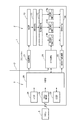
- FIG. 4 is a diagram showing the configuration of the signal processing unit 26 according to the upper model.
- the signal processing unit 26 has a configuration in which four signal processing circuits 51 are mounted on a circuit board 50. Specifically, one signal processing circuit 51 to which the color video signal D is input is mounted at the front stage of the circuit board 50.
- the signal processing circuit 51 mounted in the previous stage is appropriately given “51X” as a code, and is expressed as “signal processing circuit 51X”.
- the signal processing circuit 51 provided correspondingly to the liquid crystal light valve 17R is appropriately denoted by “51R” as a code, and is expressed as “signal processing circuit 51R”.
- the signal processing circuit 51 corresponding to the liquid crystal light valve 17G is “signal processing circuit 51G”
- the signal processing circuit 51 provided corresponding to the liquid crystal light valve 17B is “signal processing circuit 51B”.
- Each of the signal processing circuits 51 mounted on the circuit board 50 is the same as the configuration (see FIG.
- the signal processing unit 26 according to the lower model has a configuration in which the signal processing circuit 51 is mounted on the circuit board 50 alone, while the signal processing unit 26 according to the upper model includes a plurality of circuit processing units 50.
- the signal processing circuit 51 is mounted.
- frame memories 52 are mounted corresponding to the four signal processing circuits 51 respectively.
- the operation mode of the signal processing circuit 51X is switched to the second operation mode, while each operation mode of the signal processing circuits 51R, 51G, and 51B is switched to the third operation mode Be
- a color video signal D is input to the signal processing circuit 51X.
- the signal processing circuit 51X generates red frame image data Pr, green frame image data Pg, and blue frame image data Pb based on the input color video signal D, and outputs it as signal processing circuit 51R, 51G, 51B. Do.
- the signal processing circuit 51R applies a drive voltage to the liquid crystal light valve 17R based on the input red frame image data Pr to drive the liquid crystal light valve 17R.
- the signal processing circuit 51G drives the liquid crystal light valve 17G based on the input green frame image data Pg
- the signal processing circuit 51B performs a liquid crystal light valve based on the input blue frame image data Pb. Drive 17B.
- the configuration of the signal processing circuit 51 of the signal processing unit 26 related to the lower model is the same as the configuration of the signal processing circuit 51X of the signal processing unit 26 related to the upper model. Based on this, processing of each circuit of the signal processing circuit 51X will be described below, using FIG. 3 as appropriate.
- the operation mode of the signal processing circuit 51X is switched to the second operation mode, and each circuit of the signal processing circuit 51X performs various processes in accordance with the second operation mode.
- the video signal input circuit 56 of the signal processing circuit 51X according to the second operation mode executes the same processing as the video signal input circuit 56 according to the first operation mode.
- the video signal input circuit 56 generates frame image data P based on the input color video signal D, and outputs the frame image data P to the RGB image processing circuit 57.
- the RGB image processing circuit 57 of the signal processing circuit 51X according to the second operation mode executes the same processing as the RGB image processing circuit 57 according to the first operation mode. That is, predetermined processing is performed on the input frame image data P, and red frame image data Pr, which is image data of a red component for one frame, and green frame image, which is image data of a green component for one frame. Data Pg and blue frame image data Pb which is image data of a blue component for one frame are generated. Then, the RGB image processing circuit 57 applies the red frame image data Pr to the first image processing circuit 591, the green frame image data Pg to the second image processing circuit 592, and the blue frame image data Pb to the third image processing circuit 593. Output each.
- the first image processing circuit 591 of the signal processing circuit 51X according to the second operation mode outputs the input red frame image data Pr to the drive signal control circuit 60 without performing image processing.
- the second image processing circuit 592 and the third image processing circuit 593 of the signal processing circuit 51X according to the second operation mode execute image processing on the input green frame image data Pg and blue frame image data Pb. Output to the drive signal control circuit 60.
- each of the first image processing circuit 591, the second image processing circuit 592, and the third image processing circuit 593 does not execute image processing, and thus uses the frame memory 52. do not do.
- the liquid crystal light valves 17R, 17G, and 17B according to the upper model have high resolution, and therefore, high processing power is provided to a circuit that performs image processing on red frame image data Pr, green frame image data Pg, and blue frame image data Pb Desired.
- each of the first image processing circuit 591, the second image processing circuit 592, and the third image processing circuit 593 does not execute the image processing, so the processing capability of these circuits is insufficient. There is no delay in processing.
- the processing capabilities of the first image processing circuit 591, the second image processing circuit 592, and the third image processing circuit 593 satisfy the required processing capabilities for the following reasons. .
- each image processing circuit in the first operation mode and the third operation mode, each image processing circuit must be operated at the driving frequency (for example, 240 fps) of the liquid crystal light valve.
- each image processing circuit in the second operation mode, each image processing circuit is operated to correspond to the input frame rate (for example, 60 fps) or the intermediate frame generation circuit output frame rate (for example, 120 fps). Because it is good.
- the drive signal control circuit 60 of the signal processing circuit 51X according to the second operation mode outputs the red frame image data Pr input from the first image processing circuit 591 to the liquid crystal light valve drive circuit 61R.
- the drive signal control circuit 60 controls the green frame image data Pg and the blue frame image data Pb inputted from the second image processing circuit 592, the third image processing circuit 593, the liquid crystal light valve drive circuit 61G and the liquid crystal light, respectively. It outputs to the valve drive circuit 61B.
- the liquid crystal light valve drive circuit 61R of the signal processing circuit 51X according to the second operation mode is connected to the video signal input circuit 56 of the signal processing circuit 51R according to the third operation mode via the signal line (bus). ing.
- the liquid crystal light valve drive circuit 61R outputs the input red frame image data Pr as a signal to the video signal input circuit 56 of the signal processing circuit 51R.
- the liquid crystal light valve drive circuit 61G is connected to the video signal input circuit 56 of the signal processing circuit 51G via a signal line (bus).
- the liquid crystal light valve drive circuit 61G outputs the input green frame image data Pg as a signal to the video signal input circuit 56 of the signal processing circuit 51G.
- the liquid crystal light valve drive circuit 61B is connected to the video signal input circuit 56 of the signal processing circuit 51B via a signal line (bus). Then, the liquid crystal light valve drive circuit 61B outputs the input blue frame image data Pb as a signal to the video signal input circuit 56 of the signal processing circuit 51B.
- the configuration of the signal processing circuit 51 of the signal processing unit 26 related to the lower model is the same as the configuration of the signal processing circuit 51R of the signal processing unit 26 related to the upper model. Based on this, processing of each circuit of the signal processing circuit 51R will be described below, using FIG. 3 as appropriate.
- the operation mode of the signal processing circuit 51R is switched to the third operation mode, and each circuit of the signal processing circuit 51R executes various processes according to the third operation mode.
- the signal processing circuit 51R will be described below, the signal processing circuit 51R, the signal processing circuit 51G, and the configuration and operation mode of the signal processing circuit 51B are the same, and these signal processing circuits are also described below. Execute the same process as.
- the video signal input circuit 56 of the signal processing circuit 51R according to the third operation mode receives red frame image data Pr from the liquid crystal light valve drive circuit 61R of the signal processing circuit 51X according to the second operation mode.
- the video signal input circuit 56 outputs the input red frame image data Pr to the RGB image processing circuit 57.
- the RGB image processing circuit 57 of the signal processing circuit 51R according to the third operation mode does not perform image processing on the input red frame image data Pr, and the first image processing circuit 591 is processed via the frame memory controller 58.
- Output to The first image processing circuit 591 of the signal processing circuit 51R according to the third operation mode integrally controls the second image processing circuit 592-fourth image processing circuit 594, and cooperates with these circuits to form a red frame image. Image processing is performed on data Pr.
- the first image processing circuit 591 to the fourth image processing circuit 594 distribute and execute image processing on the red frame image data Pr.
- the first image processing circuit 591 causes the second image processing circuit 592 to the fourth image processing circuit 594 to execute image processing of 1 on the red frame image data Pr cyclically in a time division manner; Distribute and execute one process in each circuit.
- one process is an image processing circuit of one (for example, the second image processing circuit 592), and another process is another image It is executed by the processing circuit (for example, the fourth image processing circuit 594).
- the processing executed by the first image processing circuit 591 to the fourth image processing circuit 594 of the signal processing circuit 51R according to the third operation mode in a distributed manner is performed based on the characteristics of the liquid crystal light valve 17R and individual differences. Processing is included. As described above, in the third operation mode, image processing on frame image data of one color is performed by the four circuits of the first image processing circuit 591 to the fourth image processing circuit 594 in a distributed manner. Processing load is reduced.
- the liquid crystal light valve 17R according to the upper model has a high resolution, and therefore, a circuit that performs image processing on the red frame image data Pr is required to have high processing capability.
- the signal processing unit 26 related to the third mode can execute various processes related to the upper model with the same configuration as the configuration of the signal processing unit 26 related to the first operation mode.
- the first image processing circuit 591 of the signal processing circuit 51R according to the third operation mode cooperates with the second image processing circuit 592-fourth image processing circuit 594 to input the red frame image data Pr.
- a drive signal related to driving of the liquid crystal light valve drive circuit 61R is generated based on the processed red frame image data Pr, and is output to the drive signal control circuit 60.
- the drive signal control circuit 60 of the signal processing circuit 51R according to the third operation mode applies a drive voltage to the liquid crystal light valve 17R based on the inputted drive signal to drive the liquid crystal light valve, and is arranged in a matrix Changes the light transmittance of each pixel.
- the light transmitted through the liquid crystal light valve 17R is modulated in accordance with the image to be projected.
- the processing of each circuit of the signal processing circuit 51R has been described above, but the respective circuits of the signal processing circuits 51G and 51B also execute the same processing. That is, the signal processing circuit 51G performs dispersion processing on the input green frame image data Pg with four circuits of the first image processing circuit 591 to the fourth image processing circuit 594, and the liquid crystal light valve 17G is processed based on the processing result. To drive.
- the signal processing circuit 51B performs dispersion processing of the inputted blue frame image data Pb by the four circuits of the first image processing circuit 591 to the fourth image processing circuit 594, and the liquid crystal light valve 17B is processed based on the processing result. To drive.
- the signal processing unit 26 related to the lower model has one signal processing circuit 51, while the signal processing unit 26 related to the upper model has four signal processing circuits 51. doing.
- the configuration of each signal processing circuit 51 is the same.
- the signal processing part 26 which concerns on any model also has the processing capability according to a model. Therefore, there is no need to change the configuration of the signal processing circuit 51 according to the model.
- the frame memory 52 mounted on the circuit board 50 according to the upper model does not have to have higher performance than the frame memory 52 mounted on the circuit board 50 according to the lower model.
- the signal processing circuit 51 processes and outputs an input signal to the circuit board 50, and the video signal input circuit 56, an RGB image processing circuit 57 (pre-stage signal processing circuit) and the first image processing circuit 591-third that performs processing to be applied to the signal processed by the RGB image processing circuit 57 (pre-stage signal processing circuit) on the input signal
- An image processing circuit 593 post-stage signal processing circuit
- the signal processing circuit 51 processes the signal input to the circuit main body 54 by the stage signal processing circuit, and then processes and outputs the signal by the rear stage signal processing circuit, the circuit main body 54 A second operation mode in which the signal input to the circuit is processed by the previous stage signal processing circuit and output, or the third operation mode in which the signal input to the circuit main body 54 is processed by the subsequent stage signal processing circuit
- the operation mode is configured to be switchable to any one of the operation modes. According to this configuration, for the processing system (the signal processing unit 26 in the present embodiment) having a low required processing capacity, one signal processing circuit 51 is provided, and the state of the one signal processing circuit 51 is By switching to the operating mode, it is possible to meet the required processing power.
- a plurality of signal processing circuits 51 can be provided by providing the signal processing circuit 51 of the second operation mode at the front stage and the signal processing circuit 51 of the third operation mode at the rear stage. It is possible to execute distributed processing and to meet the required processing power. In either case, both the processing by the front stage signal processing circuit and the processing by the rear stage signal processing circuit are performed. Further, the configuration of the signal processing circuit 51 is common to both the case where the signal processing circuit 51 is used alone as the processing system and the case where a plurality of signal processing circuits 51 are used. For this reason, it is not necessary to use signal processing circuits having different processing capabilities, ie, different configurations, in accordance with the required processing capability in constructing a processing system, and it is possible to achieve cost reduction.
- the RGB image processing circuit 57 pre-stage signal processing circuit
- the first to fourth image processing circuits 591 to 594 post-stage signal processing circuit
- the frame memory 52 memory
- data based on the signal output from the RGB image processing circuit 57 is temporarily stored in the frame memory 52
- a signal based on the data temporarily stored in the frame memory 52 is a first image processing circuit 591-fourth image processing circuit 594.
- the signal is input to at least one circuit of (post-stage signal processing circuit).
- the signal processing circuit 51 may be used alone or a processing system may be constructed. It is possible to select whether to use multiple processing systems.
- a plurality of first image processing circuits 591 to third image processing circuits 593 are provided for each color as the post-stage signal processing circuits. Then, the first image processing circuit 591 to the third image processing circuit 593 receive the video signal for each color and execute processing based on the input video signal of the corresponding color.
- a processing system is constructed using one signal processing circuit 51, and the required processing If the capability is high, a plurality of signal processing circuits 51 can be used to construct a processing system. That is, it is possible to construct a processing system according to the processing capacity while reducing the cost.
- the present invention is applied to the signal processing circuit related to the projector as an example, but the present invention is applied not only to the signal processing circuit used for the projector but also to a circuit that executes processing on the input signal. It is widely applicable. Further, the device on which the signal processing circuit according to the present invention is mounted is not limited to the projector.
- each functional unit of the projector 1 illustrated in FIG. 1 indicates a functional configuration realized by cooperation of hardware and software, and a specific implementation form is not particularly limited.
- the specific detailed configuration of each part of the projector 1 can be arbitrarily changed without departing from the scope of the present invention.
Landscapes
- Engineering & Computer Science (AREA)
- Theoretical Computer Science (AREA)
- Physics & Mathematics (AREA)
- Computer Hardware Design (AREA)
- General Physics & Mathematics (AREA)
- Signal Processing (AREA)
- Multimedia (AREA)
- Chemical & Material Sciences (AREA)
- Crystallography & Structural Chemistry (AREA)
- Control Of Indicators Other Than Cathode Ray Tubes (AREA)
- Controls And Circuits For Display Device (AREA)
- Liquid Crystal Display Device Control (AREA)
- Projection Apparatus (AREA)
- Video Image Reproduction Devices For Color Tv Systems (AREA)
Priority Applications (3)
| Application Number | Priority Date | Filing Date | Title |
|---|---|---|---|
| US15/031,541 US9894334B2 (en) | 2013-11-11 | 2014-11-06 | Signal processing circuit, circuit substrate, and projector |
| CN201480061616.8A CN105723446B (zh) | 2013-11-11 | 2014-11-06 | 信号处理电路、电路基板以及投影仪 |
| KR1020167014571A KR101820346B1 (ko) | 2013-11-11 | 2014-11-06 | 신호 처리 회로, 회로 기판 및 프로젝터 |
Applications Claiming Priority (2)
| Application Number | Priority Date | Filing Date | Title |
|---|---|---|---|
| JP2013232789A JP6206104B2 (ja) | 2013-11-11 | 2013-11-11 | 信号処理回路、回路基板、及び、プロジェクター |
| JP2013-232789 | 2013-11-11 |
Publications (1)
| Publication Number | Publication Date |
|---|---|
| WO2015068396A1 true WO2015068396A1 (ja) | 2015-05-14 |
Family
ID=53041190
Family Applications (1)
| Application Number | Title | Priority Date | Filing Date |
|---|---|---|---|
| PCT/JP2014/005591 Ceased WO2015068396A1 (ja) | 2013-11-11 | 2014-11-06 | 信号処理回路、回路基板、及び、プロジェクター |
Country Status (6)
| Country | Link |
|---|---|
| US (1) | US9894334B2 (https=) |
| JP (1) | JP6206104B2 (https=) |
| KR (1) | KR101820346B1 (https=) |
| CN (1) | CN105723446B (https=) |
| TW (1) | TWI621903B (https=) |
| WO (1) | WO2015068396A1 (https=) |
Families Citing this family (2)
| Publication number | Priority date | Publication date | Assignee | Title |
|---|---|---|---|---|
| CN110442384A (zh) * | 2018-05-02 | 2019-11-12 | 姚震 | 具有多操作模式切换的装置以及操作模式切换方法 |
| CN110956910B (zh) | 2018-09-26 | 2023-05-26 | 中强光电股份有限公司 | 投影装置及其投影方法 |
Citations (4)
| Publication number | Priority date | Publication date | Assignee | Title |
|---|---|---|---|---|
| JPS63137376A (ja) * | 1986-11-29 | 1988-06-09 | Toshiba Corp | 高速回転回路 |
| JP2003256826A (ja) * | 2002-02-28 | 2003-09-12 | Ricoh Co Ltd | 画像処理回路、複合画像処理回路、および、画像形成装置 |
| JP2005227401A (ja) * | 2004-02-10 | 2005-08-25 | Pioneer Electronic Corp | サブフィールドコーディング回路、映像信号処理回路、プラズマ表示装置 |
| JP2014096746A (ja) * | 2012-11-12 | 2014-05-22 | Sony Corp | 画像処理装置及び画像処理方法 |
Family Cites Families (10)
| Publication number | Priority date | Publication date | Assignee | Title |
|---|---|---|---|---|
| JP4221183B2 (ja) * | 2002-02-19 | 2009-02-12 | 株式会社日立製作所 | 液晶表示装置 |
| JP2006072231A (ja) | 2004-09-06 | 2006-03-16 | Sony Corp | 投射型表示装置 |
| JP4816563B2 (ja) * | 2006-07-06 | 2011-11-16 | セイコーエプソン株式会社 | 画像表示システム |
| JP2008172594A (ja) | 2007-01-12 | 2008-07-24 | Ricoh Co Ltd | 画像処理装置及び画像処理方法 |
| JP2008211310A (ja) | 2007-02-23 | 2008-09-11 | Seiko Epson Corp | 画像処理装置および画像表示装置 |
| JP4450014B2 (ja) * | 2007-05-30 | 2010-04-14 | セイコーエプソン株式会社 | プロジェクタ、画像表示装置、および、画像処理装置 |
| TWI464510B (zh) * | 2007-07-20 | 2014-12-11 | Semiconductor Energy Lab | 液晶顯示裝置 |
| JP2009274253A (ja) | 2008-05-13 | 2009-11-26 | Sharp Corp | 印字制御装置 |
| CN103380453B (zh) * | 2010-12-21 | 2016-11-09 | 晶典有限公司 | 具有存储减少器的空间光调制器 |
| JP6232778B2 (ja) * | 2013-06-27 | 2017-11-22 | セイコーエプソン株式会社 | 画像処理装置、画像表示装置、および画像処理装置の制御方法 |
-
2013
- 2013-11-11 JP JP2013232789A patent/JP6206104B2/ja not_active Expired - Fee Related
-
2014
- 2014-11-06 WO PCT/JP2014/005591 patent/WO2015068396A1/ja not_active Ceased
- 2014-11-06 KR KR1020167014571A patent/KR101820346B1/ko active Active
- 2014-11-06 CN CN201480061616.8A patent/CN105723446B/zh active Active
- 2014-11-06 US US15/031,541 patent/US9894334B2/en active Active
- 2014-11-07 TW TW103138819A patent/TWI621903B/zh active
Patent Citations (4)
| Publication number | Priority date | Publication date | Assignee | Title |
|---|---|---|---|---|
| JPS63137376A (ja) * | 1986-11-29 | 1988-06-09 | Toshiba Corp | 高速回転回路 |
| JP2003256826A (ja) * | 2002-02-28 | 2003-09-12 | Ricoh Co Ltd | 画像処理回路、複合画像処理回路、および、画像形成装置 |
| JP2005227401A (ja) * | 2004-02-10 | 2005-08-25 | Pioneer Electronic Corp | サブフィールドコーディング回路、映像信号処理回路、プラズマ表示装置 |
| JP2014096746A (ja) * | 2012-11-12 | 2014-05-22 | Sony Corp | 画像処理装置及び画像処理方法 |
Also Published As
| Publication number | Publication date |
|---|---|
| US9894334B2 (en) | 2018-02-13 |
| CN105723446B (zh) | 2018-02-02 |
| TWI621903B (zh) | 2018-04-21 |
| KR20160079087A (ko) | 2016-07-05 |
| JP6206104B2 (ja) | 2017-10-04 |
| CN105723446A (zh) | 2016-06-29 |
| US20160269699A1 (en) | 2016-09-15 |
| JP2015094799A (ja) | 2015-05-18 |
| KR101820346B1 (ko) | 2018-01-19 |
| TW201518846A (zh) | 2015-05-16 |
Similar Documents
| Publication | Publication Date | Title |
|---|---|---|
| JP3843973B2 (ja) | プロジェクタ | |
| JP6897386B2 (ja) | マルチプロジェクションシステム、プロジェクターおよびプロジェクターの制御方法 | |
| US7712902B2 (en) | Projector | |
| US20200382750A1 (en) | Method of controlling display device, and display device | |
| JP6206104B2 (ja) | 信号処理回路、回路基板、及び、プロジェクター | |
| JP5845663B2 (ja) | 画像処理装置、画像表示装置及びプロジェクター | |
| US10587851B2 (en) | Projector and method of controlling projector | |
| JP6314439B2 (ja) | 表示装置、及び、表示装置の制御方法 | |
| JP4539099B2 (ja) | 投射型表示装置、投射型表示装置の制御方法、および画像出力機器 | |
| JP2011227348A (ja) | 投写型表示装置 | |
| JP2009210765A (ja) | プロジェクタ | |
| JP2019041189A (ja) | 画像投射装置およびその制御方法 | |
| JP4729911B2 (ja) | 画像表示方法およびプロジェクタ | |
| WO2024196742A1 (en) | Display levels for dual modulation systems | |
| JP2024067478A (ja) | プロジェクターの制御方法、プロジェクター、及びプログラム | |
| JP5156550B2 (ja) | 投写型映像表示装置 | |
| JP2017102313A (ja) | 画像処理装置、表示装置、及び、画像処理装置の制御方法 | |
| JP2020118780A (ja) | 画像表示装置 | |
| JP2009103917A (ja) | 投写型映像表示装置 | |
| JP2020056974A (ja) | 表示装置、表示システム、表示装置の制御方法および表示システムの制御方法 | |
| JP2007219355A (ja) | プロジェクタ | |
| JP2017059871A (ja) | 画像表示装置、および画像表示装置の制御方法 | |
| JP2011085825A (ja) | 映像表示装置 |
Legal Events
| Date | Code | Title | Description |
|---|---|---|---|
| 121 | Ep: the epo has been informed by wipo that ep was designated in this application |
Ref document number: 14860250 Country of ref document: EP Kind code of ref document: A1 |
|
| WWE | Wipo information: entry into national phase |
Ref document number: 15031541 Country of ref document: US |
|
| NENP | Non-entry into the national phase |
Ref country code: DE |
|
| ENP | Entry into the national phase |
Ref document number: 20167014571 Country of ref document: KR Kind code of ref document: A |
|
| 122 | Ep: pct application non-entry in european phase |
Ref document number: 14860250 Country of ref document: EP Kind code of ref document: A1 |