WO2015064256A1 - 炭化シリコン半導体装置及びその製造方法 - Google Patents
炭化シリコン半導体装置及びその製造方法 Download PDFInfo
- Publication number
- WO2015064256A1 WO2015064256A1 PCT/JP2014/075628 JP2014075628W WO2015064256A1 WO 2015064256 A1 WO2015064256 A1 WO 2015064256A1 JP 2014075628 W JP2014075628 W JP 2014075628W WO 2015064256 A1 WO2015064256 A1 WO 2015064256A1
- Authority
- WO
- WIPO (PCT)
- Prior art keywords
- silicon carbide
- carbide semiconductor
- semiconductor device
- layer
- sic
- Prior art date
- Legal status (The legal status is an assumption and is not a legal conclusion. Google has not performed a legal analysis and makes no representation as to the accuracy of the status listed.)
- Ceased
Links
Images


Classifications
-
- H—ELECTRICITY
- H10—SEMICONDUCTOR DEVICES; ELECTRIC SOLID-STATE DEVICES NOT OTHERWISE PROVIDED FOR
- H10P—GENERIC PROCESSES OR APPARATUS FOR THE MANUFACTURE OR TREATMENT OF DEVICES COVERED BY CLASS H10
- H10P14/00—Formation of materials, e.g. in the shape of layers or pillars
- H10P14/20—Formation of materials, e.g. in the shape of layers or pillars of semiconductor materials
- H10P14/34—Deposited materials, e.g. layers
- H10P14/3402—Deposited materials, e.g. layers characterised by the chemical composition
- H10P14/3404—Deposited materials, e.g. layers characterised by the chemical composition being Group IVA materials
- H10P14/3408—Silicon carbide
-
- H—ELECTRICITY
- H10—SEMICONDUCTOR DEVICES; ELECTRIC SOLID-STATE DEVICES NOT OTHERWISE PROVIDED FOR
- H10D—INORGANIC ELECTRIC SEMICONDUCTOR DEVICES
- H10D62/00—Semiconductor bodies, or regions thereof, of devices having potential barriers
- H10D62/50—Physical imperfections
- H10D62/53—Physical imperfections the imperfections being within the semiconductor body
-
- H—ELECTRICITY
- H10—SEMICONDUCTOR DEVICES; ELECTRIC SOLID-STATE DEVICES NOT OTHERWISE PROVIDED FOR
- H10D—INORGANIC ELECTRIC SEMICONDUCTOR DEVICES
- H10D62/00—Semiconductor bodies, or regions thereof, of devices having potential barriers
- H10D62/80—Semiconductor bodies, or regions thereof, of devices having potential barriers characterised by the materials
- H10D62/83—Semiconductor bodies, or regions thereof, of devices having potential barriers characterised by the materials being Group IV materials, e.g. B-doped Si or undoped Ge
- H10D62/832—Semiconductor bodies, or regions thereof, of devices having potential barriers characterised by the materials being Group IV materials, e.g. B-doped Si or undoped Ge being Group IV materials comprising two or more elements, e.g. SiGe
- H10D62/8325—Silicon carbide
-
- H—ELECTRICITY
- H10—SEMICONDUCTOR DEVICES; ELECTRIC SOLID-STATE DEVICES NOT OTHERWISE PROVIDED FOR
- H10D—INORGANIC ELECTRIC SEMICONDUCTOR DEVICES
- H10D64/00—Electrodes of devices having potential barriers
- H10D64/01—Manufacture or treatment
- H10D64/012—Manufacture or treatment of electrodes comprising a Schottky barrier to a semiconductor
- H10D64/0121—Manufacture or treatment of electrodes comprising a Schottky barrier to a semiconductor to Group IV semiconductors
- H10D64/0123—Manufacture or treatment of electrodes comprising a Schottky barrier to a semiconductor to Group IV semiconductors to silicon carbide
-
- H—ELECTRICITY
- H10—SEMICONDUCTOR DEVICES; ELECTRIC SOLID-STATE DEVICES NOT OTHERWISE PROVIDED FOR
- H10D—INORGANIC ELECTRIC SEMICONDUCTOR DEVICES
- H10D64/00—Electrodes of devices having potential barriers
- H10D64/60—Electrodes characterised by their materials
- H10D64/64—Electrodes comprising a Schottky barrier to a semiconductor
-
- H—ELECTRICITY
- H10—SEMICONDUCTOR DEVICES; ELECTRIC SOLID-STATE DEVICES NOT OTHERWISE PROVIDED FOR
- H10D—INORGANIC ELECTRIC SEMICONDUCTOR DEVICES
- H10D8/00—Diodes
- H10D8/01—Manufacture or treatment
- H10D8/051—Manufacture or treatment of Schottky diodes
-
- H—ELECTRICITY
- H10—SEMICONDUCTOR DEVICES; ELECTRIC SOLID-STATE DEVICES NOT OTHERWISE PROVIDED FOR
- H10D—INORGANIC ELECTRIC SEMICONDUCTOR DEVICES
- H10D8/00—Diodes
- H10D8/60—Schottky-barrier diodes
-
- H—ELECTRICITY
- H10—SEMICONDUCTOR DEVICES; ELECTRIC SOLID-STATE DEVICES NOT OTHERWISE PROVIDED FOR
- H10P—GENERIC PROCESSES OR APPARATUS FOR THE MANUFACTURE OR TREATMENT OF DEVICES COVERED BY CLASS H10
- H10P14/00—Formation of materials, e.g. in the shape of layers or pillars
- H10P14/20—Formation of materials, e.g. in the shape of layers or pillars of semiconductor materials
- H10P14/29—Formation of materials, e.g. in the shape of layers or pillars of semiconductor materials characterised by the substrates
- H10P14/2901—Materials
- H10P14/2902—Materials being Group IVA materials
- H10P14/2904—Silicon carbide
-
- H—ELECTRICITY
- H10—SEMICONDUCTOR DEVICES; ELECTRIC SOLID-STATE DEVICES NOT OTHERWISE PROVIDED FOR
- H10P—GENERIC PROCESSES OR APPARATUS FOR THE MANUFACTURE OR TREATMENT OF DEVICES COVERED BY CLASS H10
- H10P14/00—Formation of materials, e.g. in the shape of layers or pillars
- H10P14/20—Formation of materials, e.g. in the shape of layers or pillars of semiconductor materials
- H10P14/38—Formation of materials, e.g. in the shape of layers or pillars of semiconductor materials characterised by treatments done after the formation of the materials
- H10P14/3802—Crystallisation or recrystallisation of non-monocrystalline semiconductor materials, e.g. regrowth
- H10P14/3808—Crystallisation or recrystallisation of non-monocrystalline semiconductor materials, e.g. regrowth using laser beams
-
- H—ELECTRICITY
- H10—SEMICONDUCTOR DEVICES; ELECTRIC SOLID-STATE DEVICES NOT OTHERWISE PROVIDED FOR
- H10P—GENERIC PROCESSES OR APPARATUS FOR THE MANUFACTURE OR TREATMENT OF DEVICES COVERED BY CLASS H10
- H10P14/00—Formation of materials, e.g. in the shape of layers or pillars
- H10P14/20—Formation of materials, e.g. in the shape of layers or pillars of semiconductor materials
- H10P14/38—Formation of materials, e.g. in the shape of layers or pillars of semiconductor materials characterised by treatments done after the formation of the materials
- H10P14/3802—Crystallisation or recrystallisation of non-monocrystalline semiconductor materials, e.g. regrowth
- H10P14/3818—Crystallisation or recrystallisation of non-monocrystalline semiconductor materials, e.g. regrowth using particle beams
-
- H—ELECTRICITY
- H10—SEMICONDUCTOR DEVICES; ELECTRIC SOLID-STATE DEVICES NOT OTHERWISE PROVIDED FOR
- H10P—GENERIC PROCESSES OR APPARATUS FOR THE MANUFACTURE OR TREATMENT OF DEVICES COVERED BY CLASS H10
- H10P30/00—Ion implantation into wafers, substrates or parts of devices
- H10P30/20—Ion implantation into wafers, substrates or parts of devices into semiconductor materials, e.g. for doping
- H10P30/202—Ion implantation into wafers, substrates or parts of devices into semiconductor materials, e.g. for doping characterised by the semiconductor materials
- H10P30/204—Ion implantation into wafers, substrates or parts of devices into semiconductor materials, e.g. for doping characterised by the semiconductor materials into Group IV semiconductors
-
- H—ELECTRICITY
- H10—SEMICONDUCTOR DEVICES; ELECTRIC SOLID-STATE DEVICES NOT OTHERWISE PROVIDED FOR
- H10P—GENERIC PROCESSES OR APPARATUS FOR THE MANUFACTURE OR TREATMENT OF DEVICES COVERED BY CLASS H10
- H10P30/00—Ion implantation into wafers, substrates or parts of devices
- H10P30/20—Ion implantation into wafers, substrates or parts of devices into semiconductor materials, e.g. for doping
- H10P30/202—Ion implantation into wafers, substrates or parts of devices into semiconductor materials, e.g. for doping characterised by the semiconductor materials
- H10P30/204—Ion implantation into wafers, substrates or parts of devices into semiconductor materials, e.g. for doping characterised by the semiconductor materials into Group IV semiconductors
- H10P30/2042—Ion implantation into wafers, substrates or parts of devices into semiconductor materials, e.g. for doping characterised by the semiconductor materials into Group IV semiconductors into crystalline silicon carbide
-
- H—ELECTRICITY
- H10—SEMICONDUCTOR DEVICES; ELECTRIC SOLID-STATE DEVICES NOT OTHERWISE PROVIDED FOR
- H10P—GENERIC PROCESSES OR APPARATUS FOR THE MANUFACTURE OR TREATMENT OF DEVICES COVERED BY CLASS H10
- H10P30/00—Ion implantation into wafers, substrates or parts of devices
- H10P30/20—Ion implantation into wafers, substrates or parts of devices into semiconductor materials, e.g. for doping
- H10P30/208—Ion implantation into wafers, substrates or parts of devices into semiconductor materials, e.g. for doping of electrically inactive species
-
- H—ELECTRICITY
- H10—SEMICONDUCTOR DEVICES; ELECTRIC SOLID-STATE DEVICES NOT OTHERWISE PROVIDED FOR
- H10P—GENERIC PROCESSES OR APPARATUS FOR THE MANUFACTURE OR TREATMENT OF DEVICES COVERED BY CLASS H10
- H10P30/00—Ion implantation into wafers, substrates or parts of devices
- H10P30/20—Ion implantation into wafers, substrates or parts of devices into semiconductor materials, e.g. for doping
- H10P30/21—Ion implantation into wafers, substrates or parts of devices into semiconductor materials, e.g. for doping of electrically active species
-
- H—ELECTRICITY
- H10—SEMICONDUCTOR DEVICES; ELECTRIC SOLID-STATE DEVICES NOT OTHERWISE PROVIDED FOR
- H10P—GENERIC PROCESSES OR APPARATUS FOR THE MANUFACTURE OR TREATMENT OF DEVICES COVERED BY CLASS H10
- H10P30/00—Ion implantation into wafers, substrates or parts of devices
- H10P30/20—Ion implantation into wafers, substrates or parts of devices into semiconductor materials, e.g. for doping
- H10P30/218—Ion implantation into wafers, substrates or parts of devices into semiconductor materials, e.g. for doping characterised by the implantation in a compound semiconductor of both electrically active and inactive species in the same semiconductor region to be doped n-type or p-type
-
- H—ELECTRICITY
- H10—SEMICONDUCTOR DEVICES; ELECTRIC SOLID-STATE DEVICES NOT OTHERWISE PROVIDED FOR
- H10D—INORGANIC ELECTRIC SEMICONDUCTOR DEVICES
- H10D62/00—Semiconductor bodies, or regions thereof, of devices having potential barriers
- H10D62/10—Shapes, relative sizes or dispositions of the regions of the semiconductor bodies; Shapes of the semiconductor bodies
- H10D62/102—Constructional design considerations for preventing surface leakage or controlling electric field concentration
- H10D62/103—Constructional design considerations for preventing surface leakage or controlling electric field concentration for increasing or controlling the breakdown voltage of reverse-biased devices
- H10D62/105—Constructional design considerations for preventing surface leakage or controlling electric field concentration for increasing or controlling the breakdown voltage of reverse-biased devices by having particular doping profiles, shapes or arrangements of PN junctions; by having supplementary regions, e.g. junction termination extension [JTE]
- H10D62/106—Constructional design considerations for preventing surface leakage or controlling electric field concentration for increasing or controlling the breakdown voltage of reverse-biased devices by having particular doping profiles, shapes or arrangements of PN junctions; by having supplementary regions, e.g. junction termination extension [JTE] having supplementary regions doped oppositely to or in rectifying contact with regions of the semiconductor bodies, e.g. guard rings with PN or Schottky junctions
Definitions
- the present invention relates to a silicon carbide semiconductor device related to reduction of crystal defect density on the surface of a silicon carbide epitaxial layer and a method for manufacturing the same.
- silicon carbide semiconductor devices have attracted attention as devices that can exceed the characteristic limits of silicon devices.
- silicon carbide semiconductor devices have power that makes use of excellent physical properties such as higher dielectric breakdown field strength (about 10 times higher) and higher thermal conductivity (about 3 times higher) than silicon semiconductor devices. Application to semiconductor devices is expected.
- the SiC crystal ingot which is the raw material of the SiC substrate is not good in the stability of the melt at a high temperature, so it is difficult to grow a crystal from the melt like Si, and is generally produced by a sublimation method.
- a SiC semiconductor wafer cut out from an ingot produced by this sublimation method is used as a base substrate, and a SiC layer is epitaxially grown on the SiC base substrate by a vapor phase method, and an impurity diffusion layer is formed on the SiC epitaxial layer (hereinafter referred to as SiC epi layer).
- SiC epi layer SiC epitaxial layer
- SiC epi layer SiC epitaxial layer
- SiC device is manufactured by building a junction structure.
- a device similar to the Si device can be applied to the device for forming the SiC epilayer.
- the thermal diffusion method is used for forming the impurity diffusion layer. It differs greatly in that it cannot be used.
- the impurity diffusion layer is formed by the formation of a diffusion layer by multi-stage (multiple) high-temperature ion implantation with different ion implantation conditions depending on the depth of the diffusion layer and its activation.
- high temperature heat treatment at 1600 ° C. or higher is required.
- the SiC device is a vertical device in which current flows in the direction between both main surfaces of the semiconductor substrate. Therefore, if there is a crystal defect in the current path of the semiconductor substrate, the electrical characteristics of the device deteriorate and the yield rate of the product decreases. .
- SiC-SBD SiC-Shotky Barrier Diode
- SiC-MOSFET SiC-MOSFET
- the defects on the surface of the SiC epilayer include dislocation defects in which threading screw dislocations (TSD) and threading edge dislocations (TED), which inherited the defects of the SiC base substrate serving as the base, are extended to the upper epilayer, and during epi growth It is roughly divided into defects (downholes, etc.) formed in the epi layer.
- TSD threading screw dislocations
- TED threading edge dislocations
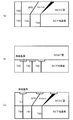
- FIG. 2 (a) shows that the TSD formed on the SiC base substrate propagates to the surface of the epi layer as it is by the conventional manufacturing method in which the SiC epi layer is formed without introducing the strained layer, or crystal defects.
- a cross section of an SiC semiconductor device in which the type is converted to a basal plane dislocation (hereinafter referred to as BPD) or carrot defect and propagates to the epilayer surface is schematically shown.
- defects such as down holes
- defects that occur during the formation of the epi layer are being reduced by improving the epi layer forming apparatus and forming conditions.
- Defects that extend through the epi layer and pass through dislocation defects such as TSD and TED generated in the SiC base substrate described above are not yet under sufficient control, and in particular, carrot-type defects that form uneven patterns on the surface. The fact is that it is almost impossible to control.
- the carrot defect is said to be a defect related to the screw dislocation and the basal plane dislocation.
- FIG. 5 (1) shows a completed section of SiC-SBD
- FIG. 5 (2) shows an outline of the manufacturing process.
- the Si surface side of the n-type SiC base substrate 1 (impurity concentration> 1 ⁇ 10 18 cm ⁇ 3 , substrate thickness 350 ⁇ m) is subjected to chemical mechanical polishing (CMP). Then, an epilayer formation pretreatment is performed.
- CMP chemical mechanical polishing
- an n-type SiC epilayer 2 (impurity concentration, about 1 ⁇ 10 16 cm ⁇ 3 , substrate thickness 10 ⁇ m) is deposited on this Si surface.
- n-type SiC epilayer 2 impurity concentration, about 1 ⁇ 10 16 cm ⁇ 3 , substrate thickness 10 ⁇ m
- CVD growth is performed at a growth temperature of 1700 ° C.
- Nitrogen (N 2 ) is used as the n-type dopant.
- an SBD peripheral breakdown voltage structure is formed on the surface of the SiC epi layer 2. That is, a p-type ion implantation region having a predetermined depth (Xj) is formed by multi-stage ion implantation of Al, B, or the like, and then heat treatment is performed at about 1600 ° C. to activate the implanted ion species. A p-type region 3 having a relaxation function is formed.
- an Ni vapor deposition film is formed on the back side of the SiC base substrate 1 and then heat-treated at about 1000 ° C. to form an ohmic Ni silicide film 4. Thereafter, a contact hole of the oxide film 5 is formed on the surface of the SiC epi layer 2 on the surface side of the SiC base substrate, and then a Schottky barrier electrode 6 such as Ti is formed. A silicide layer such as Ti silicide is formed at the junction between the Schottky barrier electrode 6 and the SiC epi layer 2 by heat treatment at about 500 ° C.
- step (e) in the figure an AlSi electrode film 7 is formed on the front surface side, and a Ti / Ni / Au electrode 8 is formed on the back surface, thereby completing the SBD device.
- the defects on the surface of the SiC epilayer are likely to affect the surface side silicide layer forming the SBD Schottky barrier and the gate oxide film quality of the MOSFET.
- the Schottky barrier height changes due to the generation of defects, and the leakage current may increase.
- these surface defects often have stepped steps on the SiC surface, the formation of the silicide layer at the stepped portions is not uniform, which may be a local electric field concentration point. Therefore, as described above, in the actual device manufacturing process, it is a general practice to exclude chips having a specific defect type from the manufacturing process at the stage of evaluating the defect distribution on the epilayer surface. Among these surface defects, the most frequent defect type is a carrot defect.
- Patent Documents 1 and 2 disclose a method of reducing defects by optimizing a buffer layer at the initial stage of crystal growth.
- Patent Document 3 discloses a method in which defects such as MyPropipe are filled in the middle and do not reach the surface by selecting the growth conditions of the epi layer.
- Patent Document 4 discloses that the growth of the epitaxial silicon carbide layer is interrupted and etched, thereby reducing the thickness of the epi layer and terminating the carrot defect, and then re-applying the second layer of epitaxial silicon carbide.
- a method of reducing carrot defects on the epilayer surface by a growing process is disclosed.
- Patent Document 5 discloses a method for reducing a reverse leakage mode by forming an oxide film on a surface defect of a SiC base substrate by an anodic oxidation method and then forming a Schottky electrode. Yes.
- the defect density on the epilayer surface is already determined when the SiC epilayer is deposited on the SiC base substrate. After the formation of the epi layer, it is only how to surely remove the device including the defect, and there is no content in Patent Documents 1 to 4 showing a method for reducing the defect itself on the surface of the epi layer.
- Patent Documents 1 to 4 showing a method for reducing the defect itself on the surface of the epi layer.
- Patent Document 5 it is possible to reduce the reverse leakage mode due to surface defects after the formation of the epi layer, but the anodic oxidation method has a problem in terms of mass productivity. is there.
- an object of the present invention is to provide a silicon carbide semiconductor device and a method for manufacturing the same that reduce the crystal defect density on the surface of the epitaxial layer and improve the yield rate of devices after forming the SiC epitaxial layer on the SiC base substrate. There is.
- a silicon carbide semiconductor device of the present invention includes a silicon carbide semiconductor device having a first conductivity type silicon carbide semiconductor epitaxial layer laminated on one main surface of a first conductivity type silicon carbide semiconductor substrate.
- a recrystallized layer is provided on at least one of the surface of the silicon carbide semiconductor substrate on which the silicon carbide semiconductor epitaxial layer is stacked and the surface of the silicon carbide semiconductor epitaxial layer.
- the recrystallized layer is selectively formed at a position covering a crystal defect penetrating the silicon carbide semiconductor epitaxial layer.
- the silicon carbide semiconductor device is preferably a silicon carbide Schottky barrier diode or a silicon carbide MOSFET.
- a method for manufacturing a silicon carbide semiconductor device is the method for manufacturing a silicon carbide semiconductor device in which a first conductivity type silicon carbide semiconductor epitaxial layer is formed on one main surface of a first conductivity type silicon carbide semiconductor substrate. Strain energy is supplied to a surface layer of at least one of a surface of a silicon carbide semiconductor substrate on which a silicon carbide semiconductor epitaxial layer is formed and a surface of the silicon carbide semiconductor epitaxial layer, and then the surface layer to which the strain energy is supplied And a step of forming a recrystallized layer by applying a heat treatment for recrystallizing the crystal.
- the means for imparting strain energy is any one of ion implantation, plasma treatment, electron beam irradiation, and proton irradiation.
- the ion species used for the ion implantation is preferably an ion species having the same conductivity type as that of the silicon carbide semiconductor substrate.
- the ion species used for the ion implantation is preferably any one selected from tetravalent elements C, Si, and Ge.
- the ion species used for the ion implantation is preferably a rare gas element.
- the rare gas element is preferably any element selected from He, Ne, and Ar.
- the heat treatment for recrystallizing the surface layer is a heat treatment using a high frequency induction heating method or a laser irradiation method.
- the heat treatment for recrystallization of the surface layer for reducing carrot defects is performed at a temperature of 1600 ° C. to 2000 ° C. for 30 seconds to 180 seconds. Preferably there is.
- a strain layer can be formed by introducing strain energy into an underlying substrate or epitaxial layer of a silicon carbide semiconductor, and the strain layer can be recrystallized by heat treatment to eliminate surface defects. Therefore, a device formation region free from crystal defects can be obtained, and a silicon carbide semiconductor excellent in electrical characteristics can be provided.
- the silicon carbide semiconductor device of the present invention is a recrystallized layer obtained by forming a strained layer on a SiC base substrate or SiC epilayer and then recrystallizing the strained layer by heat treatment in order to reduce the defect density of the SiC epilayer. Can be provided.
- the threading screw dislocation (TSD) formed on the SiC base substrate is propagated to the surface of the epi layer as it is by the conventional manufacturing method of forming the SiC epi layer without introducing the strained layer.
- TSD threading screw dislocation
- a cross section of the SiC semiconductor device in which the type of crystal defects is converted into basal plane dislocations (BPD) or carrot defects and propagates to the epilayer surface is schematically shown.
- BPD basal plane dislocations
- carrot defects propagates to the epilayer surface
- a recrystallized layer is formed by partially recrystallizing so as to cover at least the surface defects of the SiC base substrate in accordance with the manufacturing method of the present invention.
- FIG. 2C shows a SiC semiconductor device in which a defect density is reduced by forming a SiC epitaxial layer on a SiC base substrate according to the manufacturing method of the present invention and partially recrystallizing the surface of the epitaxial layer.
- the cross section of is schematically shown.
- crystal defects are also formed on the surface of the SiC epilayer, that is, the device formation region. According to the embodiments of FIGS. Can be reduced.
- the recrystallized layer in the silicon carbide semiconductor device of the present invention is in the embodiment shown in FIG. 2 (b) and / or FIG. 2 (c).
- the recrystallized layer may be partially formed on the SiC base substrate, but may be formed on the entire surface.
- an n-type SiC epilayer (doping concentration 1 ⁇ 10 16 cm ⁇ 3 ) is formed on the Si surface of a SiC base substrate (n-doped, specific resistance 20 m ⁇ cm, off angle 4 °), An epitaxial layer thickness of 10 ⁇ m is formed, and Al is implanted into the surface of the SiC epitaxial layer in three stages (first stage: 5 ⁇ 10 14 cm ⁇ 2 / 350 keV, second stage: 3 ⁇ 10 14 cm ⁇ 2 / 250 keV, Third stage: 2 ⁇ 10 14 cm ⁇ 2 / 100 keV, implantation temperature 500 ° C.), strain energy is introduced into the crystal lattice by elastic collision of ions, and a strain layer can be formed in the crystal lattice. Thereafter, the strained layer can be recrystallized by, for example, high frequency induction heating (1600 ° C., 180 seconds) to form a recrystallized layer.
- high frequency induction heating (1600 ° C., 180 seconds
- the defect density of about 5 / cm 2 immediately after SiC epitaxial, which is detected by the optical surface inspection apparatus, can be reduced to 2 / cm 2 or less after the recrystallization treatment. it can.
- FIG. 3 (a) shows a transmission electron microscope (TEM) image of a cross section of the SiC epilayer produced under the above manufacturing conditions.
- the threading dislocation defect 10 extending from the inside of the SiC base substrate (downward in the figure) to the surface of the epilayer 2 (upward in the figure) disappears at the ion implantation region boundary 11 and reaches the surface of the SiC epilayer 2.
- FIG. 5B shows a cross-sectional TEM image of a SiC epilayer that has been heat-treated without ion implantation (heat-treated without giving strain energy). It can be seen that threading dislocation defects 10 extending from the substrate reach the surface of the SiC epi layer 2 and inhibit formation of the silicide layer. Furthermore, since the silicide layer is not well formed on the threading dislocation defect 10 reaching the surface, crack-like defects (zigzag lines) are formed in the silicide.
- TEM transmission electron microscope
- the strained layer can be recrystallized, and crystal defects can be eliminated in the recrystallized layer.
- the recrystallized layer is obtained by ion implantation and high-frequency induction heating, but the present invention is not limited to this.
- the process of forming the recrystallized layer on the SiC epilayer or the SiC base substrate includes a step of applying strain energy to form the strained layer, and a step of recrystallizing the strained layer by heat treatment.
- Table 1 is a list of strain introduction methods and recrystallization methods according to the present invention.
- means for forming the strained layer ion implantation, plasma treatment, electron beam irradiation, and proton irradiation can be used. Further, heat treatment such as high-frequency induction heating or laser annealing can be used as a means for recrystallization.
- an n-type dopant N 2 , P, etc.
- a p-type dopant B, Al, etc.
- a tetravalent element C, Si
- the strained layer can be formed by ion implantation of any of rare gas elements (He, Ne, Ar, etc.). When an element having a large mass number is used, a large amount of strain energy can be introduced. However, when using an n-type dopant or a p-type dopant, the dose must be limited so as not to affect the electrical characteristics of the device. The depth of the strained layer and / or the degree of strain can be changed according to the acceleration voltage and the dose.
- the strain energy distribution can also be varied.
- three-stage ion implantation (first stage: 5 ⁇ 10 14 cm ⁇ 2 / 350 keV, second stage: 3 ⁇ 10 14 cm ⁇ 2 / 250 keV, third stage: 2 ⁇ 10 14 cm by -2 / 100 keV), it is possible to form the strained layer depth of about 1 [mu] m.
- a strained layer having a depth of about 0.2 ⁇ m can be formed.
- surface devices such as SBDs and MOSFETs
- a depth of about 1 ⁇ m is sufficient for the strained layer.
- the substrate temperature at the time of ion implantation is not particularly limited and may be 500 ° C. which is commonly used in a semiconductor process, but is not necessarily a high temperature and may be room temperature.
- the strained layer can be formed by exposing the SiC epilayer or the SiC base substrate to plasma of H, Ar, CF 4 or the like.
- the plasma device is not particularly limited, and an inductively coupled plasma device, a capacitively coupled plasma device, a microwave plasma device, or the like can be used.
- the entire surface of the SiC semiconductor substrate can be distorted by a plasma treatment of 3 hundred watts or more for 60 seconds.
- the strained layer can be formed by irradiating the SiC epilayer or the SiC base substrate with an electron beam. Since the electron beam has a high penetrating power, distortion is applied to a depth of several hundred ⁇ m at an acceleration voltage similar to that of the silicon semiconductor process. Therefore, for this purpose, it is preferable to obtain a weakly transmissive electron beam with a low-acceleration electron gun or a moderator such as an aluminum plate and control the depth and energy amount of the strained layer by the number of irradiations.
- the strained layer can be formed by irradiating the SiC epilayer or the SiC base substrate with protons accelerated by the tandem type vandegraft.
- a strain region having a peak at a depth of about 3 ⁇ m from the surface can be formed by irradiating protons at a dose of 1 ⁇ 10 13 atoms / cm 2 and an acceleration energy of 0.5 MeV.
- Heat treatment method high frequency induction heating or laser annealing can be used.
- the heat treatment is preferably performed at 1600 ° C. to 2000 ° C. for 30 seconds to 180 seconds, more preferably at 1700 ° C. to 2000 ° C. for 30 seconds to 150 seconds. If it is less than 1600 ° C., there is a high possibility that recrystallization is incomplete and crystal defects remain, and if it is 2000 ° C. or more, the dopant is sublimated and the electrical characteristics change, which is not preferable.
- laser annealing after the epilayer is formed, selective laser irradiation is performed along the defect map created by the surface defect evaluation apparatus, thereby covering only the defective portion as shown in FIGS. 2B and 2C. Thus, it is possible to selectively recrystallize the SiC surface.
- step bunching in which the irregularities on the substrate surface become severe.
- each atomic layer grows laterally in an epitaxial layer grown on a base substrate tilted about 8 degrees in the [11-20] direction from the (0001) plane of 4H—SiC.
- the growth steps at the edge are integrated under certain conditions, resulting in severe surface irregularities.
- Step bunching can be prevented by forming a carbon film with a thickness of, for example, 30 nm on the substrate surface before the heat treatment. After the heat treatment, the unnecessary carbon film can be peeled off.
- a method of smoothing by CMP after ion implantation may be used. However, it is necessary to make sure that the polishing depth in CMP is shallower than the depth of the ion implantation region so that the recrystallized layer is not excessively etched.
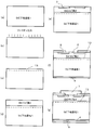
- Example 1 A SiC-SBD was manufactured according to the manufacturing process shown in FIG.
- step (b) phosphorus is ion-implanted into the entire Si surface of the SiC base substrate 1 to form an ion implantation region (strain layer).
- the dose amount was 2 ⁇ 10 15 cm ⁇ 2 and the acceleration energy was 250 keV
- the dose amount was 5 ⁇ 10 14 cm ⁇ 2 and the acceleration energy was 70 keV.
- the injection temperature was room temperature.
- step (c) heat treatment is performed for 180 seconds at a temperature of 1600 ° C. in a normal pressure Ar atmosphere by high-frequency induction heat treatment, and the ion implantation region (strain layer) introduced in step (b) is recrystallized.
- the recrystallized layer 13 was formed (the heat treatment at a temperature of 1600 ° C. for 180 seconds may be a heat treatment at 2000 ° C. for 30 seconds).
- the heat treatment at a temperature of 1600 ° C. for 180 seconds may be a heat treatment at 2000 ° C. for 30 seconds.
- a carbon film thickness 30 nm was formed on the substrate surface, and after heat treatment at 1600 ° C., peeling was performed.
- the SiC epi layer 2 was formed.
- the SiC epi layer 2 first forms a buffer layer (n-doped, carrier concentration 1 ⁇ 10 18 cm ⁇ 3 , thickness of about 0.5 ⁇ m) (not shown), and then n ⁇ -type SiC (n-type doped). And a carrier concentration of 1 ⁇ 10 16 cm ⁇ 3 and a thickness of about 10 ⁇ m).
- a p-type region 3 was formed by ion implantation of p-type dopant Al using an oxide film mask (not shown) formed by photoetching on the surface of the SiC epilayer 2.
- Implantation conditions are as follows: first stage: 5 ⁇ 10 12 cm ⁇ 2 / 350 keV, second stage: 3 ⁇ 10 12 cm ⁇ 2 / 150 keV, third stage: 2 ⁇ 10 12 cm ⁇ 2 / 100 keV did.
- the injection temperature was 500 ° C.
- a carbon film (not shown) was deposited to a thickness of 50 nm on the surface of the SiC epilayer 2, and activation heat treatment was performed at 1600 ° C. for 180 seconds. Thereafter, the carbon film was removed.
- a Ni film was formed on the back surface side, and then heat treated at 1000 ° C. to form a Ni silicide film 4.
- contact holes were formed in the oxide film 5 on the surface side by photoetching, and then a Ti film serving as the Schottky barrier electrode 6 was formed with a thickness of 200 nm. After removing Ti around the contact hole by photoetching, heat treatment was performed at 500 ° C. to form Ti silicide.
- an AlSi electrode 7 having a thickness of 5 ⁇ m was formed on the surface, and the peripheral portion was removed by a photoetching step. On the back side, a Ti / Ni / Au electrode 8 was formed on the entire surface.
- Example 1 a recrystallized layer is formed on the surface of the SiC base substrate 1 by P ion implantation and heat treatment at 1600 ° C., and the surface defect density of the SiC base substrate 1 is reduced.
- the defect extension from the SiC base substrate 1 to the SiC epi layer was prevented, and the yield rate of SiC-SBD was improved.
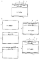
- Example 2 A SiC-SBD was fabricated according to the manufacturing process shown in FIG.
- an n ⁇ type SiC epi layer 2 (1 ⁇ 10 16 cm ⁇ 3 , 10 ⁇ m) was formed on the Si surface side of the SiC base substrate 1 (here, the n ⁇ type SiC epi layer 2 A buffer layer (1 ⁇ 10 18 cm ⁇ 3 , 0.5 ⁇ m) may be formed before the formation).
- the surface defect evaluation apparatus was used to detect 4 defects / cm 2 .
- Al oxide was ion-implanted in three stages using an oxide film mask (not shown) formed on the surface of the SiC epi layer 2 by photoetching to form a breakdown voltage structure.
- Implantation conditions are as follows: first stage: 5 ⁇ 10 12 cm ⁇ 2 / 350 keV, second stage: 3 ⁇ 10 12 cm ⁇ 2 / 150 keV, third stage: 2 ⁇ 10 12 cm ⁇ 2 / 100 keV Thus, the p-type region 3 was formed.
- the injection temperature was 500 ° C.
- a step (d) after the oxide film 5 was formed on the entire surface, the inner peripheral portion of the pressure-resistant structure portion was opened by a photoetching step, and then Ar was ion-implanted in three stages.
- the implantation conditions are as follows: first stage: dose 1 ⁇ 10 13 cm ⁇ 2 / 350 keV, second stage: 6 ⁇ 10 12 cm ⁇ 2 / 150 keV, third stage: 4 ⁇ 10 12 cm ⁇ 2 / 100 keV, room temperature Ion implantation.
- step (e) the surface oxide film was removed to form a 40 nm carbon film (not shown) on the surface, and then heat treatment was performed by high-frequency induction heating at 1700 ° C. for 150 seconds. Thereafter, to surface defect inspection, usually 4 / cm 2, the defect levels, and confirmed that it is reduced to 1.5 / cm 2.
- an oxide film 5 is formed on the surface of the SiC epi layer 2, the oxide film is partially etched away to open a contact portion of the Schottky barrier electrode 6, and then the metal of the Schottky barrier electrode 6 is formed.
- a Ti film having a thickness of 200 nm was formed and silicided by heat treatment at 500 ° C. for 30 minutes to form a Schottky barrier junction having a predetermined Schottky barrier height.
- an AlSi electrode film 7 was formed on the front surface, and a Ti / Ni / Au electrode film 8 was formed on the back surface.
- Example 2 a recrystallized layer is formed on the surface of the SiC epilayer 2 by Ar ion implantation and heat treatment at 1700 ° C., the surface defect density of the SiC epilayer 2 is reduced, and the yield rate of SiC-SBD is improved. Improved.
- the ion implantation for forming the recrystallized layer 13 on the surface of the SiC epilayer 2 basically does not matter the ion species, but has little influence on the stability of the next step of forming the Schottky junction.
- implantation of rare gas ions such as Ar is effective, that plasma treatment, electron beam irradiation, and proton irradiation are effective in addition to ion implantation, and that laser annealing is also effective as heat treatment. ing.
Landscapes
- Electrodes Of Semiconductors (AREA)
- Recrystallisation Techniques (AREA)
Abstract
Description

本発明の炭化シリコン半導体装置の製造工程では、SiCエピ層又はSiC下地基板に、n型ドーパント(N2,P等)、p型ドーパント(B,Al等)、4価元素(C,Si,Ge等)、希ガス元素(He,Ne,Ar等)のいずれかをイオン注入して、歪層を形成することができる。質量数の大きい元素を用いると、歪エネルギーを多く導入することができる。ただし、n型ドーパント又はp型ドーパントを使用する場合は、デバイスの電気特性に影響しないように、ドーズ量を制限する必要がある。歪層の深さ及び/又は歪の度合いは、加速電圧とドーズ量によって変えることができる。特に、加速電圧とドーズ量を変えてイオン注入を複数回行う、多段イオン注入法によれば、歪エネルギー分布も変えることができる。例えば、Alのイオン注入では、3段イオン注入(第1段:5×1014cm-2/350keV、第2段:3×1014cm-2/250keV、第3段:2×1014cm-2/100keV)によって、深さ約1μmの歪層を形成することができる。また、SiC-n型基板へのPの注入では、2段イオン注入(第1段:1.5×1013cm-2/70keV、第2段:1.5×1013cm-2/40keV)によって、深さ約0.2μmの歪層を形成することができる。SBDやMOSFET等の表面デバイスでは、歪層は1μm程度の深さで十分であり、更に多段イオン注入を多用して歪層を深くするとコストアップになるので好ましくない。一方、イオン注入時の基板温度は、特に制限されず、半導体プロセスで常用される500℃でもよいが、必ずしも高温である必要はなく、室温でもよい。
本発明の炭化シリコン半導体装置の製造工程では、SiCエピ層又はSiC下地基板をH、Ar、CF4等のプラズマに晒して歪層を形成することができる。プラズマ装置は、特に制限されず、誘導結合型プラズマ装置、容量結合型プラズマ装置、マイクロ波プラズマ装置等を用いることができる。例えば、容量結合型プラズマ装置によれば、3百ワット以上で60秒間のプラズマ処理によって、SiC半導体基板全面に歪を与えることができる。
本発明の炭化シリコン半導体装置の製造工程では、電子線をSiCエピ層又はSiC下地基板に照射して歪層を形成することができる。電子線は透過力が高いため、シリコン半導体プロセスと同様の加速電圧では数百μmの深さまで歪が与えられてしまう。このため、本目的に対しては、低加速電子銃、又はアルミニウム板等の減速材によって透過力の弱い電子線を得て、照射回数で歪層の深さやエネルギー量を制御することが好ましい。
本発明の炭化シリコン半導体装置の製造工程では、タンデム型バンデグラフトによって加速したプロトンをSiCエピ層又はSiC下地基板に照射して、歪層を形成することができる。例えばプロトンをドーズ量1×10¹³atoms/cm2、加速エネルギー0.5MeVで照射して、表面から3μm付近の深さにピークを持つ歪領域を形成することができる。
熱処理方法としては、高周波誘導加熱、レーザーアニール法を用いることができる。熱処理は、1600℃~2000℃で、30秒~180秒間行うことが好ましく、1700℃~2000℃で、30秒~150秒間行うことがより好ましい。1600℃未満では再結晶化が不完全で結晶欠陥が残留する可能性が高く、2000℃以上ではドーパントが昇華して電気特性が変わるので好ましくない。レーザーアニールを用いる場合、エピ層形成後に表面欠陥評価装置により作成された欠陥マップに沿って選択的レーザー照射することによって、図2(b)、(c)に示すように、欠陥部分だけを覆うように、SiC表面を選択的に再結晶化することが可能である。
図1に示す製造工程にしたがって、SiC-SBDを作製した。
図4に示す製造工程にしたがって、SiC-SBDを作製した。
この後、表面欠陥検査を実施し、通常4個/cm2、の欠陥レベルが、1.5個/cm2まで低減されていることを確認した。
2 SiCエピ層
3 p型領域
4 Niシリサイド膜
5 酸化膜
6 ショットキーバリア電極
7 AlSi電極
8 Ti/Ni/Au電極
10 貫通転位欠陥
11 再結晶層とエピ層の境界
13 再結晶層
Claims (11)
- 第一導電型の炭化シリコン半導体基板の一方の主面に積層される第一導電型の炭化シリコン半導体エピタキシャル層を有する炭化シリコン半導体装置において、
前記炭化シリコン半導体エピタキシャル層が積層される炭化シリコン半導体基板表面と炭化シリコン半導体エピタキシャル層の表面の少なくともいずれか一方の表面に再結晶層を備えることを特徴とする炭化シリコン半導体装置。 - 前記再結晶層が炭化シリコン半導体エピタキシャル層を貫通する結晶欠陥上を覆う位置に選択的に形成されていることを特徴とする請求項1記載の炭化シリコン半導体装置。
- 前記炭化シリコン半導体装置が炭化シリコンショットキーバリアダイオードまたは炭化シリコンMOSFETであることを特徴とする請求項1または2記載の炭化シリコン半導体装置。
- 第一導電型の炭化シリコン半導体基板の一方の主面に第一導電型の炭化シリコン半導体エピタキシャル層を形成する炭化シリコン半導体装置の製造方法において、前記炭化シリコン半導体エピタキシャル層が形成される炭化シリコン半導体基板の表面と前記炭化シリコン半導体エピタキシャル層の表面の少なくともいずれかの表面層に歪エネルギーを供給し、その後、前記歪エネルギーが供給された前記表面層を再結晶化させるための熱処理を加えて再結晶層を形成する工程を有することを特徴とする炭化シリコン半導体装置の製造方法。
- 前記歪エネルギーを与える手段が、イオン注入、プラズマ処理、電子線照射、プロトン照射のいずれかであることを特徴とする請求項4記載の炭化シリコン半導体装置の製造方法。
- 前記イオン注入に用いられるイオン種が、炭化シリコン半導体基板と同導電型のイオン種であることを特徴とする請求項5記載の炭化シリコン半導体装置の製造方法。
- 前記イオン注入に用いられるイオン種が、4価元素のC、Si、Geから選ばれるいずれかであることを特徴とする請求項5記載の炭化シリコン半導体装置の製造方法。
- 前記イオン注入に用いられるイオン種が、希ガス元素であることを特徴とする請求項5記載の炭化シリコン半導体装置の製造方法。
- 前記希ガス元素が、He、Ne、Arから選ばれるいずれかの元素であることを特徴とする請求項8記載の炭化シリコン半導体装置の製造方法
- 前記表面層を再結晶化させるための熱処理が、高周波誘導加熱法またはレーザー照射法を用いる加熱処理であることを特徴とする請求項4記載の炭化シリコン半導体装置の製造方法。
- キャロット欠陥を低減するための前記表面層の再結晶化のための前記加熱処理が、温度1600℃~2000℃で、30秒~180秒間の熱処理であることを特徴とする請求項10記載の炭化シリコン半導体装置の製造方法。
Priority Applications (3)
| Application Number | Priority Date | Filing Date | Title |
|---|---|---|---|
| US15/027,423 US20160254148A1 (en) | 2013-10-28 | 2014-09-26 | Silicon carbide semiconductor device and manufacturing method for same |
| CN201480055442.4A CN105637646A (zh) | 2013-10-28 | 2014-09-26 | 碳化硅半导体装置及其制造方法 |
| JP2015544871A JPWO2015064256A1 (ja) | 2013-10-28 | 2014-09-26 | 炭化シリコン半導体装置及びその製造方法 |
Applications Claiming Priority (2)
| Application Number | Priority Date | Filing Date | Title |
|---|---|---|---|
| JP2013-222852 | 2013-10-28 | ||
| JP2013222852 | 2013-10-28 |
Publications (1)
| Publication Number | Publication Date |
|---|---|
| WO2015064256A1 true WO2015064256A1 (ja) | 2015-05-07 |
Family
ID=53003869
Family Applications (1)
| Application Number | Title | Priority Date | Filing Date |
|---|---|---|---|
| PCT/JP2014/075628 Ceased WO2015064256A1 (ja) | 2013-10-28 | 2014-09-26 | 炭化シリコン半導体装置及びその製造方法 |
Country Status (4)
| Country | Link |
|---|---|
| US (1) | US20160254148A1 (ja) |
| JP (1) | JPWO2015064256A1 (ja) |
| CN (1) | CN105637646A (ja) |
| WO (1) | WO2015064256A1 (ja) |
Cited By (7)
| Publication number | Priority date | Publication date | Assignee | Title |
|---|---|---|---|---|
| WO2017221546A1 (ja) * | 2016-06-24 | 2017-12-28 | 富士電機株式会社 | 半導体装置の製造方法および半導体装置 |
| JP2019140186A (ja) * | 2018-02-07 | 2019-08-22 | 株式会社東芝 | 半導体装置、基板、半導体装置の製造方法、及び、基板の製造方法。 |
| CN111799324A (zh) * | 2015-05-18 | 2020-10-20 | 住友电气工业株式会社 | 碳化硅外延基板、碳化硅半导体装置及其制造方法 |
| JP2021005736A (ja) * | 2018-02-07 | 2021-01-14 | 株式会社東芝 | 半導体装置、基板、半導体装置の製造方法、及び、基板の製造方法 |
| JP2021057381A (ja) * | 2019-09-27 | 2021-04-08 | 株式会社デンソー | 炭化珪素半導体装置 |
| WO2021085078A1 (ja) * | 2019-10-29 | 2021-05-06 | 国立研究開発法人産業技術総合研究所 | 炭化珪素半導体装置および炭化珪素半導体装置の製造方法 |
| WO2022158085A1 (ja) * | 2021-01-25 | 2022-07-28 | ローム株式会社 | 半導体基板及びその製造方法、及び半導体装置 |
Families Citing this family (8)
| Publication number | Priority date | Publication date | Assignee | Title |
|---|---|---|---|---|
| JP6271356B2 (ja) * | 2014-07-07 | 2018-01-31 | 株式会社東芝 | 半導体装置の製造方法 |
| CN110301034B (zh) * | 2017-02-20 | 2023-07-11 | 株式会社博迈立铖 | 碳化硅层叠基板及其制造方法 |
| JP6782263B2 (ja) * | 2018-02-07 | 2020-11-11 | 株式会社東芝 | 半導体装置、基板、半導体装置の製造方法、及び、基板の製造方法 |
| JP7023882B2 (ja) * | 2019-02-04 | 2022-02-22 | 株式会社東芝 | 半導体装置の製造方法、基板の製造方法、半導体装置、基板、及び、基板の製造装置 |
| EP4012079B1 (en) * | 2019-08-06 | 2025-10-15 | Kwansei Gakuin Educational Foundation | Method for producing a sic substrate |
| IT202200005357A1 (it) * | 2022-03-18 | 2023-09-18 | St Microelectronics Srl | Procedimento di lavorazione di una fetta di materiale 4h-sic per formare uno strato di 3c-sic in contatto diretto con il materiale 4h-sic |
| JP2024067415A (ja) * | 2022-11-04 | 2024-05-17 | 富士電機株式会社 | 炭化珪素半導体装置および炭化珪素半導体装置の製造方法 |
| CN115863174B (zh) * | 2022-12-27 | 2025-12-16 | 飞锃半导体(上海)有限公司 | 半导体结构的形成方法 |
Citations (6)
| Publication number | Priority date | Publication date | Assignee | Title |
|---|---|---|---|---|
| JP2000044398A (ja) * | 1998-05-29 | 2000-02-15 | Toyota Central Res & Dev Lab Inc | 炭化珪素単結晶の製造方法及びそれによって得られた炭化珪素単結晶 |
| JP2002261041A (ja) * | 2001-03-05 | 2002-09-13 | Shikusuon:Kk | SiC半導体のイオン注入層及びその製造方法 |
| JP2007210861A (ja) * | 2006-02-10 | 2007-08-23 | Mitsubishi Materials Corp | SiC基板の製造方法及びSiC基板並びに半導体装置 |
| JP2010153464A (ja) * | 2008-12-24 | 2010-07-08 | Toyota Central R&D Labs Inc | 半導体装置およびその製造方法 |
| JP2011168453A (ja) * | 2010-02-19 | 2011-09-01 | Denso Corp | 炭化珪素基板の製造方法 |
| JP2013058601A (ja) * | 2011-09-08 | 2013-03-28 | Toshiba Corp | 半導体装置および半導体装置の製造方法 |
Family Cites Families (9)
| Publication number | Priority date | Publication date | Assignee | Title |
|---|---|---|---|---|
| US4575923A (en) * | 1983-04-06 | 1986-03-18 | North American Philips Corporation | Method of manufacturing a high resistance layer having a low temperature coefficient of resistance and semiconductor device having such high resistance layer |
| US5545571A (en) * | 1991-08-26 | 1996-08-13 | Semiconductor Energy Laboratory Co., Ltd. | Method of making TFT with anodic oxidation process using positive and negative voltages |
| KR970003917B1 (en) * | 1992-04-07 | 1997-03-22 | Semiconductor Energy Lab Kk | Method of making insulating gate semiconductor device |
| JP3760688B2 (ja) * | 1999-08-26 | 2006-03-29 | 富士電機ホールディングス株式会社 | 炭化けい素半導体素子の製造方法 |
| JP2001332508A (ja) * | 2000-05-23 | 2001-11-30 | Matsushita Electric Ind Co Ltd | 半導体素子の製造方法 |
| JP4179492B2 (ja) * | 2000-09-01 | 2008-11-12 | 日産自動車株式会社 | オーミック電極構造体、その製造方法、及びオーミック電極を用いた半導体装置 |
| JP2007115875A (ja) * | 2005-10-20 | 2007-05-10 | Sumitomo Electric Ind Ltd | 炭化珪素半導体装置およびその製造方法 |
| JP2010177465A (ja) * | 2009-01-29 | 2010-08-12 | Oki Semiconductor Co Ltd | 半導体装置、及びその製造方法 |
| JP5799458B2 (ja) * | 2011-03-29 | 2015-10-28 | 学校法人関西学院 | 半導体素子の製造方法 |
-
2014
- 2014-09-26 WO PCT/JP2014/075628 patent/WO2015064256A1/ja not_active Ceased
- 2014-09-26 JP JP2015544871A patent/JPWO2015064256A1/ja active Pending
- 2014-09-26 US US15/027,423 patent/US20160254148A1/en not_active Abandoned
- 2014-09-26 CN CN201480055442.4A patent/CN105637646A/zh active Pending
Patent Citations (6)
| Publication number | Priority date | Publication date | Assignee | Title |
|---|---|---|---|---|
| JP2000044398A (ja) * | 1998-05-29 | 2000-02-15 | Toyota Central Res & Dev Lab Inc | 炭化珪素単結晶の製造方法及びそれによって得られた炭化珪素単結晶 |
| JP2002261041A (ja) * | 2001-03-05 | 2002-09-13 | Shikusuon:Kk | SiC半導体のイオン注入層及びその製造方法 |
| JP2007210861A (ja) * | 2006-02-10 | 2007-08-23 | Mitsubishi Materials Corp | SiC基板の製造方法及びSiC基板並びに半導体装置 |
| JP2010153464A (ja) * | 2008-12-24 | 2010-07-08 | Toyota Central R&D Labs Inc | 半導体装置およびその製造方法 |
| JP2011168453A (ja) * | 2010-02-19 | 2011-09-01 | Denso Corp | 炭化珪素基板の製造方法 |
| JP2013058601A (ja) * | 2011-09-08 | 2013-03-28 | Toshiba Corp | 半導体装置および半導体装置の製造方法 |
Cited By (21)
| Publication number | Priority date | Publication date | Assignee | Title |
|---|---|---|---|---|
| CN111799324B (zh) * | 2015-05-18 | 2024-09-13 | 住友电气工业株式会社 | 碳化硅外延基板、碳化硅半导体装置及其制造方法 |
| JP2021165229A (ja) * | 2015-05-18 | 2021-10-14 | 住友電気工業株式会社 | 炭化珪素エピタキシャル基板、炭化珪素半導体装置の製造方法および炭化珪素半導体装置 |
| CN111799324A (zh) * | 2015-05-18 | 2020-10-20 | 住友电气工业株式会社 | 碳化硅外延基板、碳化硅半导体装置及其制造方法 |
| JP7211456B2 (ja) | 2015-05-18 | 2023-01-24 | 住友電気工業株式会社 | 炭化珪素エピタキシャル基板、炭化珪素半導体装置の製造方法および炭化珪素半導体装置 |
| US10622212B2 (en) | 2016-06-24 | 2020-04-14 | Fuji Electric Co., Ltd. | Semiconductor device manufacturing method and semiconductor device |
| WO2017221546A1 (ja) * | 2016-06-24 | 2017-12-28 | 富士電機株式会社 | 半導体装置の製造方法および半導体装置 |
| US11087986B2 (en) | 2016-06-24 | 2021-08-10 | Fuji Electric Co., Ltd. | Semiconductor device manufacturing method and semiconductor device |
| JPWO2017221546A1 (ja) * | 2016-06-24 | 2018-09-27 | 富士電機株式会社 | 半導体装置の製造方法および半導体装置 |
| JP2019140186A (ja) * | 2018-02-07 | 2019-08-22 | 株式会社東芝 | 半導体装置、基板、半導体装置の製造方法、及び、基板の製造方法。 |
| JP2021005736A (ja) * | 2018-02-07 | 2021-01-14 | 株式会社東芝 | 半導体装置、基板、半導体装置の製造方法、及び、基板の製造方法 |
| JP2021057381A (ja) * | 2019-09-27 | 2021-04-08 | 株式会社デンソー | 炭化珪素半導体装置 |
| JP7331590B2 (ja) | 2019-09-27 | 2023-08-23 | 株式会社デンソー | 炭化珪素半導体装置 |
| JP7642947B2 (ja) | 2019-10-29 | 2025-03-11 | 国立研究開発法人産業技術総合研究所 | 炭化珪素半導体装置および炭化珪素半導体装置の製造方法 |
| JPWO2021085078A1 (ja) * | 2019-10-29 | 2021-05-06 | ||
| WO2021085078A1 (ja) * | 2019-10-29 | 2021-05-06 | 国立研究開発法人産業技術総合研究所 | 炭化珪素半導体装置および炭化珪素半導体装置の製造方法 |
| JP2025063267A (ja) * | 2019-10-29 | 2025-04-15 | 国立研究開発法人産業技術総合研究所 | 炭化珪素半導体装置および炭化珪素半導体装置の製造方法 |
| US12302621B2 (en) | 2019-10-29 | 2025-05-13 | Sumitomo Electric Industries, Ltd. | Silicon carbide semiconductor device and method of manufacturing silicon carbide semiconductor device |
| JP7836051B2 (ja) | 2019-10-29 | 2026-03-26 | 国立研究開発法人産業技術総合研究所 | 炭化珪素半導体装置および炭化珪素半導体装置の製造方法 |
| WO2022158085A1 (ja) * | 2021-01-25 | 2022-07-28 | ローム株式会社 | 半導体基板及びその製造方法、及び半導体装置 |
| JPWO2022158085A1 (ja) * | 2021-01-25 | 2022-07-28 | ||
| JP7846025B2 (ja) | 2021-01-25 | 2026-04-14 | ローム株式会社 | 半導体基板の製造方法 |
Also Published As
| Publication number | Publication date |
|---|---|
| JPWO2015064256A1 (ja) | 2017-03-09 |
| US20160254148A1 (en) | 2016-09-01 |
| CN105637646A (zh) | 2016-06-01 |
Similar Documents
| Publication | Publication Date | Title |
|---|---|---|
| WO2015064256A1 (ja) | 炭化シリコン半導体装置及びその製造方法 | |
| JP4185215B2 (ja) | SiCウエハ、SiC半導体デバイス、および、SiCウエハの製造方法 | |
| JP3854508B2 (ja) | SiCウエハ、SiC半導体デバイス、およびSiCウエハの製造方法 | |
| CN108292686B (zh) | 碳化硅外延基板及碳化硅半导体装置 | |
| US20170179236A1 (en) | Method of producing silicon carbide epitaxial substrate, silicon carbide epitaxial substrate, and silicon carbide semiconductor device | |
| KR100853991B1 (ko) | 바이폴라형 반도체 장치 및 그의 제조방법 | |
| JP4418794B2 (ja) | 炭化珪素半導体素子の製造方法 | |
| JP5316612B2 (ja) | 炭化珪素半導体エピタキシャル基板の製造方法 | |
| US10964785B2 (en) | SiC epitaxial wafer and manufacturing method of the same | |
| JP6239097B2 (ja) | SiCエピタキシャルウエハ | |
| WO2017073749A1 (ja) | エピタキシャルウェハの製造方法、エピタキシャルウェハ、半導体装置の製造方法及び半導体装置 | |
| JP6222771B2 (ja) | 炭化珪素半導体装置の製造方法 | |
| JP2009088223A (ja) | 炭化珪素半導体基板およびそれを用いた炭化珪素半導体装置 | |
| KR20120023710A (ko) | 반도체 장치 | |
| JPWO2001018872A1 (ja) | SiCウエハ、SiC半導体デバイス、および、SiCウエハの製造方法 | |
| JP6891758B2 (ja) | 炭化珪素エピタキシャル基板及び炭化珪素半導体装置の製造方法 | |
| JP4946264B2 (ja) | 炭化珪素半導体エピタキシャル基板の製造方法 | |
| US8367510B2 (en) | Process for producing silicon carbide semiconductor device | |
| JP4879507B2 (ja) | バイポーラ型半導体装置の順方向電圧回復方法、積層欠陥縮小方法およびバイポーラ型半導体装置 | |
| US8455269B2 (en) | Method for recovering an on-state forward voltage and, shrinking stacking faults in bipolar semiconductor devices, and the bipolar semiconductor devices | |
| JP2012253115A (ja) | エピタキシャルウエハおよびその製造方法、半導体装置およびその製造方法 | |
| Kimoto et al. | Defect Electronics in SiC and Fabrication of Ultrahigh-Voltage Bipolar Devices | |
| JP6686419B2 (ja) | シリコンゲルマニウムエピタキシャルウェーハの製造方法およびシリコンゲルマニウムエピタキシャルウェーハ | |
| JP2003347235A (ja) | 半導体装置の製造方法 | |
| WO2025115393A1 (ja) | 炭化珪素基体、炭化珪素基体の製造方法、炭化珪素半導体装置および炭化珪素半導体装置の製造方法 |
Legal Events
| Date | Code | Title | Description |
|---|---|---|---|
| 121 | Ep: the epo has been informed by wipo that ep was designated in this application |
Ref document number: 14858478 Country of ref document: EP Kind code of ref document: A1 |
|
| WWE | Wipo information: entry into national phase |
Ref document number: 15027423 Country of ref document: US |
|
| ENP | Entry into the national phase |
Ref document number: 2015544871 Country of ref document: JP Kind code of ref document: A |
|
| NENP | Non-entry into the national phase |
Ref country code: DE |
|
| 122 | Ep: pct application non-entry in european phase |
Ref document number: 14858478 Country of ref document: EP Kind code of ref document: A1 |