WO2015053002A1 - 半導体モジュール - Google Patents
半導体モジュール Download PDFInfo
- Publication number
- WO2015053002A1 WO2015053002A1 PCT/JP2014/072455 JP2014072455W WO2015053002A1 WO 2015053002 A1 WO2015053002 A1 WO 2015053002A1 JP 2014072455 W JP2014072455 W JP 2014072455W WO 2015053002 A1 WO2015053002 A1 WO 2015053002A1
- Authority
- WO
- WIPO (PCT)
- Prior art keywords
- signal
- semiconductor element
- lead
- electrode
- wire
- Prior art date
- Legal status (The legal status is an assumption and is not a legal conclusion. Google has not performed a legal analysis and makes no representation as to the accuracy of the status listed.)
- Ceased
Links
Images



Classifications
-
- H—ELECTRICITY
- H10—SEMICONDUCTOR DEVICES; ELECTRIC SOLID-STATE DEVICES NOT OTHERWISE PROVIDED FOR
- H10W—GENERIC PACKAGES, INTERCONNECTIONS, CONNECTORS OR OTHER CONSTRUCTIONAL DETAILS OF DEVICES COVERED BY CLASS H10
- H10W90/00—Package configurations
-
- H—ELECTRICITY
- H10—SEMICONDUCTOR DEVICES; ELECTRIC SOLID-STATE DEVICES NOT OTHERWISE PROVIDED FOR
- H10D—INORGANIC ELECTRIC SEMICONDUCTOR DEVICES
- H10D84/00—Integrated devices formed in or on semiconductor substrates that comprise only semiconducting layers, e.g. on Si wafers or on GaAs-on-Si wafers
- H10D84/60—Integrated devices formed in or on semiconductor substrates that comprise only semiconducting layers, e.g. on Si wafers or on GaAs-on-Si wafers characterised by the integration of at least one component covered by groups H10D10/00 or H10D18/00, e.g. integration of BJTs
- H10D84/641—Combinations of only vertical BJTs
-
- H—ELECTRICITY
- H10—SEMICONDUCTOR DEVICES; ELECTRIC SOLID-STATE DEVICES NOT OTHERWISE PROVIDED FOR
- H10W—GENERIC PACKAGES, INTERCONNECTIONS, CONNECTORS OR OTHER CONSTRUCTIONAL DETAILS OF DEVICES COVERED BY CLASS H10
- H10W70/00—Package substrates; Interposers; Redistribution layers [RDL]
- H10W70/40—Leadframes
- H10W70/421—Shapes or dispositions
- H10W70/442—Shapes or dispositions of multiple leadframes in a single chip
-
- H—ELECTRICITY
- H10—SEMICONDUCTOR DEVICES; ELECTRIC SOLID-STATE DEVICES NOT OTHERWISE PROVIDED FOR
- H10W—GENERIC PACKAGES, INTERCONNECTIONS, CONNECTORS OR OTHER CONSTRUCTIONAL DETAILS OF DEVICES COVERED BY CLASS H10
- H10W70/00—Package substrates; Interposers; Redistribution layers [RDL]
- H10W70/40—Leadframes
- H10W70/461—Leadframes specially adapted for cooling
-
- H—ELECTRICITY
- H10—SEMICONDUCTOR DEVICES; ELECTRIC SOLID-STATE DEVICES NOT OTHERWISE PROVIDED FOR
- H10W—GENERIC PACKAGES, INTERCONNECTIONS, CONNECTORS OR OTHER CONSTRUCTIONAL DETAILS OF DEVICES COVERED BY CLASS H10
- H10W70/00—Package substrates; Interposers; Redistribution layers [RDL]
- H10W70/40—Leadframes
- H10W70/464—Additional interconnections in combination with leadframes
- H10W70/465—Bumps or wires
-
- H—ELECTRICITY
- H10—SEMICONDUCTOR DEVICES; ELECTRIC SOLID-STATE DEVICES NOT OTHERWISE PROVIDED FOR
- H10W—GENERIC PACKAGES, INTERCONNECTIONS, CONNECTORS OR OTHER CONSTRUCTIONAL DETAILS OF DEVICES COVERED BY CLASS H10
- H10W70/00—Package substrates; Interposers; Redistribution layers [RDL]
- H10W70/40—Leadframes
- H10W70/464—Additional interconnections in combination with leadframes
- H10W70/466—Tape carriers or flat leads
-
- H—ELECTRICITY
- H10—SEMICONDUCTOR DEVICES; ELECTRIC SOLID-STATE DEVICES NOT OTHERWISE PROVIDED FOR
- H10W—GENERIC PACKAGES, INTERCONNECTIONS, CONNECTORS OR OTHER CONSTRUCTIONAL DETAILS OF DEVICES COVERED BY CLASS H10
- H10W70/00—Package substrates; Interposers; Redistribution layers [RDL]
- H10W70/60—Insulating or insulated package substrates; Interposers; Redistribution layers
- H10W70/62—Insulating or insulated package substrates; Interposers; Redistribution layers characterised by their interconnections
- H10W70/65—Shapes or dispositions of interconnections
- H10W70/657—Shapes or dispositions of interconnections on sidewalls or bottom surfaces of the package substrates, interposers or redistribution layers
-
- H—ELECTRICITY
- H10—SEMICONDUCTOR DEVICES; ELECTRIC SOLID-STATE DEVICES NOT OTHERWISE PROVIDED FOR
- H10W—GENERIC PACKAGES, INTERCONNECTIONS, CONNECTORS OR OTHER CONSTRUCTIONAL DETAILS OF DEVICES COVERED BY CLASS H10
- H10W72/00—Interconnections or connectors in packages
-
- H—ELECTRICITY
- H10—SEMICONDUCTOR DEVICES; ELECTRIC SOLID-STATE DEVICES NOT OTHERWISE PROVIDED FOR
- H10W—GENERIC PACKAGES, INTERCONNECTIONS, CONNECTORS OR OTHER CONSTRUCTIONAL DETAILS OF DEVICES COVERED BY CLASS H10
- H10W72/00—Interconnections or connectors in packages
- H10W72/20—Bump connectors, e.g. solder bumps or copper pillars; Dummy bumps; Thermal bumps
-
- H—ELECTRICITY
- H10—SEMICONDUCTOR DEVICES; ELECTRIC SOLID-STATE DEVICES NOT OTHERWISE PROVIDED FOR
- H10W—GENERIC PACKAGES, INTERCONNECTIONS, CONNECTORS OR OTHER CONSTRUCTIONAL DETAILS OF DEVICES COVERED BY CLASS H10
- H10W90/00—Package configurations
- H10W90/811—Multiple chips on leadframes
-
- H—ELECTRICITY
- H10—SEMICONDUCTOR DEVICES; ELECTRIC SOLID-STATE DEVICES NOT OTHERWISE PROVIDED FOR
- H10W—GENERIC PACKAGES, INTERCONNECTIONS, CONNECTORS OR OTHER CONSTRUCTIONAL DETAILS OF DEVICES COVERED BY CLASS H10
- H10W72/00—Interconnections or connectors in packages
- H10W72/071—Connecting or disconnecting
- H10W72/072—Connecting or disconnecting of bump connectors
-
- H—ELECTRICITY
- H10—SEMICONDUCTOR DEVICES; ELECTRIC SOLID-STATE DEVICES NOT OTHERWISE PROVIDED FOR
- H10W—GENERIC PACKAGES, INTERCONNECTIONS, CONNECTORS OR OTHER CONSTRUCTIONAL DETAILS OF DEVICES COVERED BY CLASS H10
- H10W72/00—Interconnections or connectors in packages
- H10W72/071—Connecting or disconnecting
- H10W72/073—Connecting or disconnecting of die-attach connectors
- H10W72/07351—Connecting or disconnecting of die-attach connectors characterised by changes in properties of the die-attach connectors during connecting
- H10W72/07354—Connecting or disconnecting of die-attach connectors characterised by changes in properties of the die-attach connectors during connecting changes in dispositions
-
- H—ELECTRICITY
- H10—SEMICONDUCTOR DEVICES; ELECTRIC SOLID-STATE DEVICES NOT OTHERWISE PROVIDED FOR
- H10W—GENERIC PACKAGES, INTERCONNECTIONS, CONNECTORS OR OTHER CONSTRUCTIONAL DETAILS OF DEVICES COVERED BY CLASS H10
- H10W72/00—Interconnections or connectors in packages
- H10W72/071—Connecting or disconnecting
- H10W72/075—Connecting or disconnecting of bond wires
- H10W72/07551—Connecting or disconnecting of bond wires characterised by changes in properties of the bond wires during the connecting
- H10W72/07554—Connecting or disconnecting of bond wires characterised by changes in properties of the bond wires during the connecting changes in dispositions
-
- H—ELECTRICITY
- H10—SEMICONDUCTOR DEVICES; ELECTRIC SOLID-STATE DEVICES NOT OTHERWISE PROVIDED FOR
- H10W—GENERIC PACKAGES, INTERCONNECTIONS, CONNECTORS OR OTHER CONSTRUCTIONAL DETAILS OF DEVICES COVERED BY CLASS H10
- H10W72/00—Interconnections or connectors in packages
- H10W72/20—Bump connectors, e.g. solder bumps or copper pillars; Dummy bumps; Thermal bumps
- H10W72/251—Materials
- H10W72/252—Materials comprising solid metals or solid metalloids, e.g. PbSn, Ag or Cu
-
- H—ELECTRICITY
- H10—SEMICONDUCTOR DEVICES; ELECTRIC SOLID-STATE DEVICES NOT OTHERWISE PROVIDED FOR
- H10W—GENERIC PACKAGES, INTERCONNECTIONS, CONNECTORS OR OTHER CONSTRUCTIONAL DETAILS OF DEVICES COVERED BY CLASS H10
- H10W72/00—Interconnections or connectors in packages
- H10W72/20—Bump connectors, e.g. solder bumps or copper pillars; Dummy bumps; Thermal bumps
- H10W72/29—Bond pads specially adapted therefor
-
- H—ELECTRICITY
- H10—SEMICONDUCTOR DEVICES; ELECTRIC SOLID-STATE DEVICES NOT OTHERWISE PROVIDED FOR
- H10W—GENERIC PACKAGES, INTERCONNECTIONS, CONNECTORS OR OTHER CONSTRUCTIONAL DETAILS OF DEVICES COVERED BY CLASS H10
- H10W72/00—Interconnections or connectors in packages
- H10W72/30—Die-attach connectors
- H10W72/341—Dispositions of die-attach connectors, e.g. layouts
- H10W72/347—Dispositions of multiple die-attach connectors
-
- H—ELECTRICITY
- H10—SEMICONDUCTOR DEVICES; ELECTRIC SOLID-STATE DEVICES NOT OTHERWISE PROVIDED FOR
- H10W—GENERIC PACKAGES, INTERCONNECTIONS, CONNECTORS OR OTHER CONSTRUCTIONAL DETAILS OF DEVICES COVERED BY CLASS H10
- H10W72/00—Interconnections or connectors in packages
- H10W72/30—Die-attach connectors
- H10W72/351—Materials of die-attach connectors
- H10W72/352—Materials of die-attach connectors comprising metals or metalloids, e.g. solders
-
- H—ELECTRICITY
- H10—SEMICONDUCTOR DEVICES; ELECTRIC SOLID-STATE DEVICES NOT OTHERWISE PROVIDED FOR
- H10W—GENERIC PACKAGES, INTERCONNECTIONS, CONNECTORS OR OTHER CONSTRUCTIONAL DETAILS OF DEVICES COVERED BY CLASS H10
- H10W72/00—Interconnections or connectors in packages
- H10W72/30—Die-attach connectors
- H10W72/381—Auxiliary members
-
- H—ELECTRICITY
- H10—SEMICONDUCTOR DEVICES; ELECTRIC SOLID-STATE DEVICES NOT OTHERWISE PROVIDED FOR
- H10W—GENERIC PACKAGES, INTERCONNECTIONS, CONNECTORS OR OTHER CONSTRUCTIONAL DETAILS OF DEVICES COVERED BY CLASS H10
- H10W72/00—Interconnections or connectors in packages
- H10W72/50—Bond wires
- H10W72/531—Shapes of wire connectors
- H10W72/536—Shapes of wire connectors the connected ends being ball-shaped
-
- H—ELECTRICITY
- H10—SEMICONDUCTOR DEVICES; ELECTRIC SOLID-STATE DEVICES NOT OTHERWISE PROVIDED FOR
- H10W—GENERIC PACKAGES, INTERCONNECTIONS, CONNECTORS OR OTHER CONSTRUCTIONAL DETAILS OF DEVICES COVERED BY CLASS H10
- H10W72/00—Interconnections or connectors in packages
- H10W72/50—Bond wires
- H10W72/541—Dispositions of bond wires
- H10W72/5445—Dispositions of bond wires being orthogonal to a side surface of the chip, e.g. parallel arrangements
-
- H—ELECTRICITY
- H10—SEMICONDUCTOR DEVICES; ELECTRIC SOLID-STATE DEVICES NOT OTHERWISE PROVIDED FOR
- H10W—GENERIC PACKAGES, INTERCONNECTIONS, CONNECTORS OR OTHER CONSTRUCTIONAL DETAILS OF DEVICES COVERED BY CLASS H10
- H10W72/00—Interconnections or connectors in packages
- H10W72/50—Bond wires
- H10W72/541—Dispositions of bond wires
- H10W72/547—Dispositions of multiple bond wires
-
- H—ELECTRICITY
- H10—SEMICONDUCTOR DEVICES; ELECTRIC SOLID-STATE DEVICES NOT OTHERWISE PROVIDED FOR
- H10W—GENERIC PACKAGES, INTERCONNECTIONS, CONNECTORS OR OTHER CONSTRUCTIONAL DETAILS OF DEVICES COVERED BY CLASS H10
- H10W72/00—Interconnections or connectors in packages
- H10W72/50—Bond wires
- H10W72/551—Materials of bond wires
- H10W72/552—Materials of bond wires comprising metals or metalloids, e.g. silver
-
- H—ELECTRICITY
- H10—SEMICONDUCTOR DEVICES; ELECTRIC SOLID-STATE DEVICES NOT OTHERWISE PROVIDED FOR
- H10W—GENERIC PACKAGES, INTERCONNECTIONS, CONNECTORS OR OTHER CONSTRUCTIONAL DETAILS OF DEVICES COVERED BY CLASS H10
- H10W72/00—Interconnections or connectors in packages
- H10W72/50—Bond wires
- H10W72/59—Bond pads specially adapted therefor
-
- H—ELECTRICITY
- H10—SEMICONDUCTOR DEVICES; ELECTRIC SOLID-STATE DEVICES NOT OTHERWISE PROVIDED FOR
- H10W—GENERIC PACKAGES, INTERCONNECTIONS, CONNECTORS OR OTHER CONSTRUCTIONAL DETAILS OF DEVICES COVERED BY CLASS H10
- H10W72/00—Interconnections or connectors in packages
- H10W72/823—Interconnections through encapsulations, e.g. pillars through molded resin on a lateral side a chip
-
- H—ELECTRICITY
- H10—SEMICONDUCTOR DEVICES; ELECTRIC SOLID-STATE DEVICES NOT OTHERWISE PROVIDED FOR
- H10W—GENERIC PACKAGES, INTERCONNECTIONS, CONNECTORS OR OTHER CONSTRUCTIONAL DETAILS OF DEVICES COVERED BY CLASS H10
- H10W72/00—Interconnections or connectors in packages
- H10W72/851—Dispositions of multiple connectors or interconnections
- H10W72/853—On the same surface
- H10W72/856—Bump connectors and die-attach connectors
-
- H—ELECTRICITY
- H10—SEMICONDUCTOR DEVICES; ELECTRIC SOLID-STATE DEVICES NOT OTHERWISE PROVIDED FOR
- H10W—GENERIC PACKAGES, INTERCONNECTIONS, CONNECTORS OR OTHER CONSTRUCTIONAL DETAILS OF DEVICES COVERED BY CLASS H10
- H10W72/00—Interconnections or connectors in packages
- H10W72/851—Dispositions of multiple connectors or interconnections
- H10W72/853—On the same surface
- H10W72/865—Die-attach connectors and bond wires
-
- H—ELECTRICITY
- H10—SEMICONDUCTOR DEVICES; ELECTRIC SOLID-STATE DEVICES NOT OTHERWISE PROVIDED FOR
- H10W—GENERIC PACKAGES, INTERCONNECTIONS, CONNECTORS OR OTHER CONSTRUCTIONAL DETAILS OF DEVICES COVERED BY CLASS H10
- H10W72/00—Interconnections or connectors in packages
- H10W72/851—Dispositions of multiple connectors or interconnections
- H10W72/874—On different surfaces
- H10W72/877—Bump connectors and die-attach connectors
-
- H—ELECTRICITY
- H10—SEMICONDUCTOR DEVICES; ELECTRIC SOLID-STATE DEVICES NOT OTHERWISE PROVIDED FOR
- H10W—GENERIC PACKAGES, INTERCONNECTIONS, CONNECTORS OR OTHER CONSTRUCTIONAL DETAILS OF DEVICES COVERED BY CLASS H10
- H10W72/00—Interconnections or connectors in packages
- H10W72/851—Dispositions of multiple connectors or interconnections
- H10W72/874—On different surfaces
- H10W72/884—Die-attach connectors and bond wires
-
- H—ELECTRICITY
- H10—SEMICONDUCTOR DEVICES; ELECTRIC SOLID-STATE DEVICES NOT OTHERWISE PROVIDED FOR
- H10W—GENERIC PACKAGES, INTERCONNECTIONS, CONNECTORS OR OTHER CONSTRUCTIONAL DETAILS OF DEVICES COVERED BY CLASS H10
- H10W72/00—Interconnections or connectors in packages
- H10W72/90—Bond pads, in general
- H10W72/931—Shapes of bond pads
- H10W72/932—Plan-view shape, i.e. in top view
-
- H—ELECTRICITY
- H10—SEMICONDUCTOR DEVICES; ELECTRIC SOLID-STATE DEVICES NOT OTHERWISE PROVIDED FOR
- H10W—GENERIC PACKAGES, INTERCONNECTIONS, CONNECTORS OR OTHER CONSTRUCTIONAL DETAILS OF DEVICES COVERED BY CLASS H10
- H10W72/00—Interconnections or connectors in packages
- H10W72/90—Bond pads, in general
- H10W72/941—Dispositions of bond pads
- H10W72/944—Dispositions of multiple bond pads
- H10W72/9445—Top-view layouts, e.g. mirror arrays
-
- H—ELECTRICITY
- H10—SEMICONDUCTOR DEVICES; ELECTRIC SOLID-STATE DEVICES NOT OTHERWISE PROVIDED FOR
- H10W—GENERIC PACKAGES, INTERCONNECTIONS, CONNECTORS OR OTHER CONSTRUCTIONAL DETAILS OF DEVICES COVERED BY CLASS H10
- H10W74/00—Encapsulations, e.g. protective coatings
-
- H—ELECTRICITY
- H10—SEMICONDUCTOR DEVICES; ELECTRIC SOLID-STATE DEVICES NOT OTHERWISE PROVIDED FOR
- H10W—GENERIC PACKAGES, INTERCONNECTIONS, CONNECTORS OR OTHER CONSTRUCTIONAL DETAILS OF DEVICES COVERED BY CLASS H10
- H10W90/00—Package configurations
- H10W90/20—Configurations of stacked chips
- H10W90/231—Configurations of stacked chips the stacked chips being on both top and bottom sides of an auxiliary carrier having no electrical connection structure
-
- H—ELECTRICITY
- H10—SEMICONDUCTOR DEVICES; ELECTRIC SOLID-STATE DEVICES NOT OTHERWISE PROVIDED FOR
- H10W—GENERIC PACKAGES, INTERCONNECTIONS, CONNECTORS OR OTHER CONSTRUCTIONAL DETAILS OF DEVICES COVERED BY CLASS H10
- H10W90/00—Package configurations
- H10W90/701—Package configurations characterised by the relative positions of pads or connectors relative to package parts
- H10W90/721—Package configurations characterised by the relative positions of pads or connectors relative to package parts of bump connectors
- H10W90/724—Package configurations characterised by the relative positions of pads or connectors relative to package parts of bump connectors between a chip and a stacked insulating package substrate, interposer or RDL
-
- H—ELECTRICITY
- H10—SEMICONDUCTOR DEVICES; ELECTRIC SOLID-STATE DEVICES NOT OTHERWISE PROVIDED FOR
- H10W—GENERIC PACKAGES, INTERCONNECTIONS, CONNECTORS OR OTHER CONSTRUCTIONAL DETAILS OF DEVICES COVERED BY CLASS H10
- H10W90/00—Package configurations
- H10W90/701—Package configurations characterised by the relative positions of pads or connectors relative to package parts
- H10W90/731—Package configurations characterised by the relative positions of pads or connectors relative to package parts of die-attach connectors
- H10W90/732—Package configurations characterised by the relative positions of pads or connectors relative to package parts of die-attach connectors between stacked chips
-
- H—ELECTRICITY
- H10—SEMICONDUCTOR DEVICES; ELECTRIC SOLID-STATE DEVICES NOT OTHERWISE PROVIDED FOR
- H10W—GENERIC PACKAGES, INTERCONNECTIONS, CONNECTORS OR OTHER CONSTRUCTIONAL DETAILS OF DEVICES COVERED BY CLASS H10
- H10W90/00—Package configurations
- H10W90/701—Package configurations characterised by the relative positions of pads or connectors relative to package parts
- H10W90/731—Package configurations characterised by the relative positions of pads or connectors relative to package parts of die-attach connectors
- H10W90/734—Package configurations characterised by the relative positions of pads or connectors relative to package parts of die-attach connectors between a chip and a stacked insulating package substrate, interposer or RDL
-
- H—ELECTRICITY
- H10—SEMICONDUCTOR DEVICES; ELECTRIC SOLID-STATE DEVICES NOT OTHERWISE PROVIDED FOR
- H10W—GENERIC PACKAGES, INTERCONNECTIONS, CONNECTORS OR OTHER CONSTRUCTIONAL DETAILS OF DEVICES COVERED BY CLASS H10
- H10W90/00—Package configurations
- H10W90/701—Package configurations characterised by the relative positions of pads or connectors relative to package parts
- H10W90/731—Package configurations characterised by the relative positions of pads or connectors relative to package parts of die-attach connectors
- H10W90/736—Package configurations characterised by the relative positions of pads or connectors relative to package parts of die-attach connectors between a chip and a stacked lead frame, conducting package substrate or heat sink
-
- H—ELECTRICITY
- H10—SEMICONDUCTOR DEVICES; ELECTRIC SOLID-STATE DEVICES NOT OTHERWISE PROVIDED FOR
- H10W—GENERIC PACKAGES, INTERCONNECTIONS, CONNECTORS OR OTHER CONSTRUCTIONAL DETAILS OF DEVICES COVERED BY CLASS H10
- H10W90/00—Package configurations
- H10W90/701—Package configurations characterised by the relative positions of pads or connectors relative to package parts
- H10W90/751—Package configurations characterised by the relative positions of pads or connectors relative to package parts of bond wires
- H10W90/754—Package configurations characterised by the relative positions of pads or connectors relative to package parts of bond wires between a chip and a stacked insulating package substrate, interposer or RDL
-
- H—ELECTRICITY
- H10—SEMICONDUCTOR DEVICES; ELECTRIC SOLID-STATE DEVICES NOT OTHERWISE PROVIDED FOR
- H10W—GENERIC PACKAGES, INTERCONNECTIONS, CONNECTORS OR OTHER CONSTRUCTIONAL DETAILS OF DEVICES COVERED BY CLASS H10
- H10W90/00—Package configurations
- H10W90/701—Package configurations characterised by the relative positions of pads or connectors relative to package parts
- H10W90/751—Package configurations characterised by the relative positions of pads or connectors relative to package parts of bond wires
- H10W90/756—Package configurations characterised by the relative positions of pads or connectors relative to package parts of bond wires between a chip and a stacked lead frame, conducting package substrate or heat sink
Definitions
- the technology disclosed in this specification relates to a semiconductor module.
- Japanese Patent Application Laid-Open No. 2009-295794 discloses a semiconductor device including a pair of semiconductor elements arranged in the vertical direction.
- the pair of semiconductor elements are arranged so that the respective emitter electrodes face each other.
- Each semiconductor element is connected to a control terminal via a wire.
- the control terminals are arranged side by side with an interval in the vertical direction.
- an object of the present specification is to provide a semiconductor module that can be miniaturized.
- the semiconductor module disclosed in the present specification is arranged with a first semiconductor element having a first signal electrode formed on the surface thereof and a distance from the first semiconductor element, and is arranged on the first semiconductor element side. And a second semiconductor element having a second signal electrode formed on a surface thereof.
- the semiconductor module further includes a first signal lead electrically connected to the first signal electrode and a second signal lead electrically connected to the second signal electrode. .
- the first signal lead and the second signal lead are arranged so that their height positions are aligned in the height direction from the first semiconductor element toward the second semiconductor element.
- the first signal lead and the second signal lead are arranged so that their height positions are aligned in the height direction from the first semiconductor element to the second semiconductor element. Therefore, the width of the semiconductor module in this direction can be reduced.
- the semiconductor module includes an insulating member disposed between the first semiconductor element and the second semiconductor element, a first signal pattern formed on a surface of the insulating member on the first semiconductor element side, and a first of the insulating member. And a second signal pattern formed on the surface of the semiconductor element side.
- the first signal electrode is electrically connected to the first signal lead via the first signal pattern
- the second signal electrode is electrically connected to the second signal lead via the second signal pattern. It is connected to the.
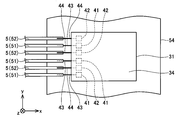
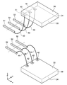
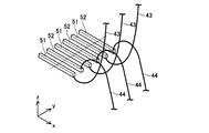
- FIG. 2 is a cross-sectional view taken along the line II-II in FIG. It is a perspective view which expands and shows a part of component of a semiconductor module. It is a perspective view which expands and shows a part of component of a semiconductor module. It is sectional drawing corresponding to FIG. 2 of the semiconductor module of other embodiment. It is a longitudinal cross-sectional view of the semiconductor module of further another embodiment. It is VII-VII sectional drawing of FIG. It is a perspective view which expands and shows a part of component of a semiconductor module. It is a longitudinal cross-sectional view of the semiconductor module of further another embodiment. Furthermore, it is sectional drawing corresponding to FIG. 2 of the semiconductor module of other embodiment.
- the semiconductor module 2 includes a pair of semiconductor elements 3 (first semiconductor element 31 and second semiconductor element 32) and a plurality of signal leads 5 (first signal elements). A lead 51 and a second signal lead 52).
- the first semiconductor element 31 and the second semiconductor element 32, and the first signal lead 51 and the second signal lead 52 are separated in the vertical direction (z direction) to make the drawing easier to see. Is shown.
- the semiconductor module 2 includes an emitter lead 53 and a collector lead 54 corresponding to each semiconductor element 3. Further, the semiconductor module 2 includes a sealing resin 6 that seals the whole.
- an IGBT Insulated Gate Bipolar Transistor
- the 1st semiconductor element 31 and the 2nd semiconductor element 32 are arrange
- the first semiconductor element 31 is disposed above the second semiconductor element 32.
- the pair of semiconductor elements 3 (first semiconductor element 31 and second semiconductor element 32) have a front surface 33 and a back surface 34, respectively, and are arranged so that the front surfaces 33 face each other.
- the surface 33 of the first semiconductor element 31 faces downward, and the surface 33 of the second semiconductor element 32 faces upward (the back surface 34 of the first semiconductor element 31 faces upward, and the back surface of the second semiconductor element 32 34 is pointing down.)
- An emitter electrode (not shown) is formed on the front surface 33 of the semiconductor element 3, and a collector electrode (not shown) is formed on the back surface 34.
- An emitter lead 53 is disposed at a position adjacent to each emitter electrode. Each emitter electrode is connected to an adjacent emitter lead 53 by solder 22.
- a collector lead 54 is disposed at a position adjacent to each collector electrode. Each collector electrode is connected to an adjacent collector lead 54 by solder 23. That is, each semiconductor element 3 is disposed between the emitter lead 53 and the collector lead 54.
- the collector lead 54 functions as a heat sink. The heat generated from each semiconductor element 3 (the first semiconductor element 31 and the second semiconductor element 32) is released to the outside through the collector lead 54 (heat sink).
- a plate-like insulating member 7 is disposed between the upper and lower emitter leads 53.
- Metal layers are formed on the front and back surfaces of the insulating member 7.
- the metal layers on the front surface and the back surface of the insulating member 7 are fixed to the emitter leads 53 by solder 24.
- the upper and lower emitter leads 53 are insulated by the insulating member 7.
- a cooler (not shown) for cooling the semiconductor element 3 is disposed outside each of the collector leads 54. Further, a sealing resin 6 for sealing the semiconductor element 3 is filled between the upper and lower collector leads 54.
- the upper first semiconductor element 31 has a plurality of first signal electrodes 41 formed on the surface 33 thereof, and the lower second semiconductor element 32 has a plurality of first electrodes formed on the surface 33 thereof.
- a two-signal electrode 42 is provided.
- Each signal electrode 4 (first signal electrode 41 and second signal electrode 42) is formed adjacent to the emitter electrode.
- the signal electrode 4 is an electrode for transmitting and receiving control signals between the semiconductor element 3 and an external device (not shown).
- the plurality of signal electrodes 4 are formed side by side in a plan view.
- the first signal electrode 41 and the second signal electrode 42 are formed to be shifted laterally so as not to overlap each other in plan view.
- the first signal electrodes 41 and the second signal electrodes 42 are alternately arranged in plan view.
- the first signal electrode 41 and the second signal electrode 42 are configured not to overlap in the vertical direction (z direction).
- Each signal lead 5 is partially covered with the sealing resin 6, and a part thereof protrudes from the sealing resin 6 to the outside.
- Each signal lead 5 (first signal lead 51 and second signal lead 52) is made of each signal electrode 4 (first signal electrode 41 and second wire 44) by a metal wire (first wire 43 and second wire 44).
- the second signal electrode 42) is connected.
- the first signal lead 51 is electrically connected to the first signal electrode 41 via the first wire 43
- the second signal lead 52 is electrically connected to the second signal electrode 42 via the second wire 44. It is connected to the.
- the signal leads 5 are arranged so as to extend in parallel with an interval.
- the first signal leads and the second signal leads are alternately arranged. Therefore, the first wire 43 and the second wire 44 are alternately arranged. As shown in FIG.
- the first wire 43 is curved so as to protrude downward.
- One end of the first wire 43 is connected to the first signal electrode 41 from the lower side of the first signal electrode 41, and the other end is connected to the first signal lead 51 from the lower side of the first signal lead 51. It is connected to the.
- the second wire 44 is curved so as to protrude upward.
- One end of the second wire 44 is connected to the second signal electrode 42 from the upper side of the second signal electrode 42, and the other end is connected to the second signal lead 52 from the upper side of the second signal lead 52.
- the signal leads 5 are arranged in a line in the horizontal direction (y direction) as shown in FIG. Further, each signal lead 5 (first signal lead 51 and second signal lead 52) is directed from the outside of the sealing resin 6 toward a region sandwiched between the semiconductor elements 3 (that is, along the x direction). ) (See FIG. 1). Each signal lead 5 (first signal lead 51 and second signal lead 52) is in the vertical direction (z direction), that is, in the height direction from the first semiconductor element 31 to the second semiconductor element 32. These are arranged so that their height positions are aligned. In the present specification, “consisting of height positions” is not strictly limited to the same height, but is a concept including a state in which the heights differ to some extent.
- the deviations in the height positions of the plurality of signal leads 5 are preferably within the range of manufacturing errors from the viewpoint of miniaturization of the semiconductor module.
- the range of manufacturing error is preferably in the range of 0 to 100 ⁇ m. That is, it is preferable that the difference between the height positions of the signal leads 5 is within 100 ⁇ m at most.
- Each signal lead 5 (the first signal lead 51 and the second signal lead 52) is the same as the first signal lead 51 when viewed along the direction in which the signal leads 5 are arranged (y direction). It is preferable that the second signal leads 52 overlap at least partially. The overlapping of the signal leads 5 when viewed along the y direction reduces the deviation of the height position of each signal lead 5 in the z direction.
- the semiconductor module 2 since the height positions of the plurality of signal leads 5 in the vertical direction (z direction) are aligned, the width in the vertical direction can be reduced. Therefore, the semiconductor module 2 can be downsized.
- the first signal electrodes 41 and the second signal electrodes 42 are alternately arranged in a plan view.
- the present invention is not limited to this configuration, and as shown in FIG. A plurality of first signal electrodes 41 may be formed on one side and the second signal electrodes 42 may be formed on the other side.
- the configuration for electrically connecting the signal electrode 4 and the signal lead 5 is not limited to the above embodiment.
- the signal electrode 4 and the signal lead 5 may be electrically connected via a signal pattern 9. 6 and FIG. 7, the same components as those in FIG. 1 and FIG.
- the semiconductor module 2 includes an insulating member 72 disposed between the pair of semiconductor elements 3, and a signal pattern 9 (a first pattern disposed on the front and back surfaces of the insulating member 72, respectively). A signal pattern 91 and a second signal pattern 92).
- the insulating member 72 is formed from a ceramic having insulating properties.
- the insulating member 72 is disposed between the first semiconductor element 31 and the second semiconductor element 32.
- a first signal pattern 91 is formed on the front surface (upper surface) of the insulating member 72, and a second signal pattern 92 is formed on the rear surface (lower surface). That is, the first signal pattern 91 is formed on the surface of the insulating member 72 on the first semiconductor element 31 side, and the second signal pattern 92 is formed on the surface of the insulating member 72 on the second semiconductor element 32 side. Yes.
- An emitter pattern 153 is formed on the front and back surfaces of the insulating member 72.
- the signal pattern 9 and the emitter pattern 153 are made of a metal such as aluminum or copper. The signal pattern 9 and the emitter pattern 153 are separated from each other.
- the signal pattern 9 is electrically connected to the signal electrode 4 (first signal electrode 41 and second signal electrode 42) via metal solder (first solder 93 and second solder 94). .
- the first signal pattern 91 is fixed to the first signal electrode 41 by the first solder 93.
- the second signal pattern 92 is fixed to the second signal electrode 42 by the second solder 94.
- the signal lead 5 (the first signal lead 51 and the second signal lead 52) is a signal pattern 9 (the first signal pattern 91 and the second signal lead) by a metal wire (the first wire 143 and the second wire 144).
- Signal pattern 92 One end of the first wire 143 is connected to the first signal pattern 91 from the upper side of the first signal pattern 91, and the other end is connected to the first signal lead 51 from the upper side as shown in FIG. It is connected to one signal lead 51.
- One end of the second wire 144 is connected to the second signal pattern 92 from the lower side of the second signal pattern 92, and the other end is the lower side of the second signal lead 52 as shown in FIG. To the second signal lead 52.
- the first wire 143 extends upward from the first signal pattern 91 and the first signal lead 51.
- the second wire 144 extends downward from the second signal pattern 92 and the second signal lead 52.
- the first signal lead 51 is electrically connected to the first signal electrode 41 via the first wire 143, the first signal pattern 91, and the first solder 93.
- the second signal lead 52 is electrically connected to the second signal electrode 42 via the second wire 144, the second signal pattern 92, and the second solder 94.
- the emitter pattern 153 is fixed to the surface 33 of each semiconductor element 3 by solder 122. As a result, the emitter electrode on the surface side of each semiconductor element 3 is electrically connected to the emitter pattern 153.
- the wires (the first wire 143 and the second wire 143) are connected.
- the contact between the wires 144) can be prevented. That is, if the signal pattern 9 is not interposed, the first wire 143 and the second wire 144 may intersect with each other, and the wires 143 and 144 may contact each other. However, since the first wire 143 and the second wire 144 do not intersect with each other through the signal pattern 9, it is possible to prevent the wires 143 and 144 from contacting each other.
- the wire is used when the signal electrode 4 and the signal lead 5 are electrically connected.
- the wire is not necessarily used.
- the signal lead 5 first signal lead 51 and second signal lead 52
- the signal pattern 9 first signal pattern 91 and second signal pattern 92.
- a connected configuration may be used. 9, the same components as those in FIG. 6 are denoted by the same reference numerals, and description thereof is omitted.
- the first signal lead 51 is bent upward, and the second signal lead 52 is bent downward.
- One end of the first signal lead 51 covers the upper surface of the first signal pattern 91, and one end of the second signal lead 52 covers the lower surface of the second signal pattern 92.
- the first signal lead 51 is fixed to the first signal pattern 91 by solder (not shown), and the second signal lead 52 is fixed to the second signal pattern 92 by solder (not shown).
- the arrangement of the plurality of signal leads 5 is not limited to the above embodiment.
- the plurality of signal leads 5 may be arranged in a state where the positions of the tip portions are shifted in the longitudinal direction. 10, the same components as those in FIG. 2 are denoted by the same reference numerals and description thereof is omitted.
- the position of the tip is shifted in three stages.
- the signal lead 5 far from the semiconductor element 3 is formed longer than the signal lead 5 close to the semiconductor element 3.
- the first signal leads 51 and the second signal leads 52 are alternately arranged.
- the direction in which the plurality of signal leads 5 (the first signal lead 51 and the second signal lead 52) extends and the direction in which the wires (the first wire 43 and the second wire 44) extend intersect each other. .
- the IGBT is used as the semiconductor element 3.
- the present invention is not limited to this, and a MOSFET or the like may be used as the semiconductor element 3.
Landscapes
- Wire Bonding (AREA)
- Cooling Or The Like Of Semiconductors Or Solid State Devices (AREA)
- Structures Or Materials For Encapsulating Or Coating Semiconductor Devices Or Solid State Devices (AREA)
Abstract
Description
3;半導体素子
4;信号用電極
5;信号用リード
6;封止樹脂
7;絶縁部材
9;信号用パターン
22;はんだ
23;はんだ
24;はんだ
31;第1半導体素子
32;第2半導体素子
33;表面
34;裏面
35;エミッタ電極
36;コレクタ電極
41;第1信号用電極
42;第2信号用電極
43;第1ワイヤ
44;第2ワイヤ
51;第1信号用リード
52;第2信号用リード
53;エミッタ用リード
54;コレクタ用リード(ヒートシンク)
72;絶縁部材
91;第1信号用パターン
92;第2信号用パターン
93;第1はんだ
94;第2はんだ
143;第1ワイヤ
144;第2ワイヤ
153;エミッタ用パターン
Claims (2)
- 表面に第1信号用電極が形成されている第1半導体素子と、
第1半導体素子に対して間隔を開けて配置されており、第1半導体素子側の表面に第2信号用電極が形成されている第2半導体素子と、
第1信号用電極に電気的に接続されている第1信号用リードと、
第2信号用電極に電気的に接続されている第2信号用リードと、を備え、
第1信号用リードと第2信号用リードは、第1半導体素子から第2半導体素子に向かう高さ方向において、それぞれの高さ位置が揃うように配置されている、半導体モジュール。 - 第1半導体素子と第2半導体素子の間に配置されている絶縁部材と、
絶縁部材の第1半導体素子側の表面に形成された第1信号用パターンと、
絶縁部材の第2半導体素子側の表面に形成された第2信号用パターンと、をさらに備え、
第1信号用電極が第1信号用パターンを介して第1信号用リードに電気的に接続されており、
第2信号用電極が第2信号用パターンを介して第2信号用リードに電気的に接続されている、請求項1に記載の半導体モジュール。
Priority Applications (3)
| Application Number | Priority Date | Filing Date | Title |
|---|---|---|---|
| US14/912,547 US20160260691A1 (en) | 2013-10-07 | 2014-08-27 | Semiconductor module |
| DE112014004620.5T DE112014004620T5 (de) | 2013-10-07 | 2014-08-27 | Halbleitermodul |
| CN201480055188.8A CN105612616A (zh) | 2013-10-07 | 2014-08-27 | 半导体模块 |
Applications Claiming Priority (2)
| Application Number | Priority Date | Filing Date | Title |
|---|---|---|---|
| JP2013-210188 | 2013-10-07 | ||
| JP2013210188A JP2015076440A (ja) | 2013-10-07 | 2013-10-07 | 半導体モジュール |
Publications (1)
| Publication Number | Publication Date |
|---|---|
| WO2015053002A1 true WO2015053002A1 (ja) | 2015-04-16 |
Family
ID=52812822
Family Applications (1)
| Application Number | Title | Priority Date | Filing Date |
|---|---|---|---|
| PCT/JP2014/072455 Ceased WO2015053002A1 (ja) | 2013-10-07 | 2014-08-27 | 半導体モジュール |
Country Status (5)
| Country | Link |
|---|---|
| US (1) | US20160260691A1 (ja) |
| JP (1) | JP2015076440A (ja) |
| CN (1) | CN105612616A (ja) |
| DE (1) | DE112014004620T5 (ja) |
| WO (1) | WO2015053002A1 (ja) |
Families Citing this family (3)
| Publication number | Priority date | Publication date | Assignee | Title |
|---|---|---|---|---|
| CN110164858B (zh) * | 2018-02-16 | 2023-05-05 | 株式会社电装 | 半导体器件 |
| JP7196761B2 (ja) * | 2019-05-15 | 2022-12-27 | 株式会社デンソー | 半導体装置 |
| US12362332B2 (en) * | 2020-07-29 | 2025-07-15 | Mitsubishi Electric Corporation | Semiconductor device |
Citations (4)
| Publication number | Priority date | Publication date | Assignee | Title |
|---|---|---|---|---|
| JP2009117723A (ja) * | 2007-11-08 | 2009-05-28 | Toyota Motor Corp | 半導体装置とその製造方法 |
| WO2009150875A1 (ja) * | 2008-06-12 | 2009-12-17 | 株式会社安川電機 | パワーモジュールおよびその制御方法 |
| WO2011083578A1 (ja) * | 2010-01-08 | 2011-07-14 | トヨタ自動車株式会社 | 半導体モジュール |
| WO2012157069A1 (ja) * | 2011-05-16 | 2012-11-22 | トヨタ自動車株式会社 | パワーモジュール |
Family Cites Families (16)
| Publication number | Priority date | Publication date | Assignee | Title |
|---|---|---|---|---|
| JP2634516B2 (ja) * | 1991-10-15 | 1997-07-30 | 三菱電機株式会社 | 反転型icの製造方法、反転型ic、icモジュール |
| TW373308B (en) * | 1995-02-24 | 1999-11-01 | Agere Systems Inc | Thin packaging of multi-chip modules with enhanced thermal/power management |
| US6181718B1 (en) * | 1997-01-08 | 2001-01-30 | Matsushita Electric Industrial Co., Ltd. | Electronically cooled semiconductor laser module with modified ground line inductance |
| US7518223B2 (en) * | 2001-08-24 | 2009-04-14 | Micron Technology, Inc. | Semiconductor devices and semiconductor device assemblies including a nonconfluent spacer layer |
| TWI322448B (en) * | 2002-10-08 | 2010-03-21 | Chippac Inc | Semiconductor stacked multi-package module having inverted second package |
| US7205656B2 (en) * | 2005-02-22 | 2007-04-17 | Micron Technology, Inc. | Stacked device package for peripheral and center device pad layout device |
| US7511371B2 (en) * | 2005-11-01 | 2009-03-31 | Sandisk Corporation | Multiple die integrated circuit package |
| US7800211B2 (en) * | 2007-06-29 | 2010-09-21 | Stats Chippac, Ltd. | Stackable package by using internal stacking modules |
| US8030743B2 (en) * | 2008-01-07 | 2011-10-04 | Fairchild Semiconductor Corporation | Semiconductor package with an embedded printed circuit board and stacked die |
| KR101454321B1 (ko) * | 2008-01-22 | 2014-10-23 | 페어차일드코리아반도체 주식회사 | 절연 금속 기판을 구비하는 반도체 패키지 및 그 제조방법 |
| JP5067267B2 (ja) * | 2008-06-05 | 2012-11-07 | 三菱電機株式会社 | 樹脂封止型半導体装置とその製造方法 |
| US9041183B2 (en) * | 2011-07-19 | 2015-05-26 | Ut-Battelle, Llc | Power module packaging with double sided planar interconnection and heat exchangers |
| US9240371B2 (en) * | 2011-08-10 | 2016-01-19 | Denso Corporation | Semiconductor module, semiconductor device having semiconductor module, and method of manufacturing semiconductor module |
| JP2013191788A (ja) * | 2012-03-15 | 2013-09-26 | Denso Corp | 半導体モジュール及び半導体装置 |
| US9123555B2 (en) * | 2013-10-25 | 2015-09-01 | Invensas Corporation | Co-support for XFD packaging |
| KR102320046B1 (ko) * | 2014-09-19 | 2021-11-01 | 삼성전자주식회사 | 캐스케이드 칩 스택을 갖는 반도체 패키지 |
-
2013
- 2013-10-07 JP JP2013210188A patent/JP2015076440A/ja active Pending
-
2014
- 2014-08-27 DE DE112014004620.5T patent/DE112014004620T5/de not_active Withdrawn
- 2014-08-27 US US14/912,547 patent/US20160260691A1/en not_active Abandoned
- 2014-08-27 WO PCT/JP2014/072455 patent/WO2015053002A1/ja not_active Ceased
- 2014-08-27 CN CN201480055188.8A patent/CN105612616A/zh active Pending
Patent Citations (4)
| Publication number | Priority date | Publication date | Assignee | Title |
|---|---|---|---|---|
| JP2009117723A (ja) * | 2007-11-08 | 2009-05-28 | Toyota Motor Corp | 半導体装置とその製造方法 |
| WO2009150875A1 (ja) * | 2008-06-12 | 2009-12-17 | 株式会社安川電機 | パワーモジュールおよびその制御方法 |
| WO2011083578A1 (ja) * | 2010-01-08 | 2011-07-14 | トヨタ自動車株式会社 | 半導体モジュール |
| WO2012157069A1 (ja) * | 2011-05-16 | 2012-11-22 | トヨタ自動車株式会社 | パワーモジュール |
Also Published As
| Publication number | Publication date |
|---|---|
| JP2015076440A (ja) | 2015-04-20 |
| CN105612616A (zh) | 2016-05-25 |
| DE112014004620T5 (de) | 2016-07-14 |
| US20160260691A1 (en) | 2016-09-08 |
Similar Documents
| Publication | Publication Date | Title |
|---|---|---|
| JP6451747B2 (ja) | 半導体装置 | |
| JP6254299B2 (ja) | 半導体モジュール | |
| JP6254300B2 (ja) | 半導体モジュール | |
| JP6790684B2 (ja) | 半導体装置 | |
| JP6805776B2 (ja) | 半導体装置 | |
| CN111886694B (zh) | 功率半导体装置 | |
| JP2015115471A (ja) | 電力用半導体装置 | |
| JP2015056638A (ja) | 半導体装置およびその製造方法 | |
| WO2015053002A1 (ja) | 半導体モジュール | |
| CN109511279B (zh) | 电子模块 | |
| US9728475B2 (en) | Lead portion of semiconductor device | |
| JP5544767B2 (ja) | 半導体装置 | |
| JP7302715B2 (ja) | 半導体装置 | |
| US9620442B2 (en) | Semiconductor device | |
| JP7035868B2 (ja) | 半導体装置 | |
| JP7160079B2 (ja) | 半導体装置 | |
| JP7069848B2 (ja) | 半導体装置 | |
| JP7407684B2 (ja) | 半導体装置 | |
| CN112993023B (zh) | 半导体模块以及半导体装置 | |
| JP2018133463A (ja) | 半導体モジュール | |
| JP6299388B2 (ja) | 半導体装置及びこれを用いた電力変換装置 | |
| JP2024046398A (ja) | 半導体装置 | |
| JP3190017U (ja) | 半導体装置 | |
| JP2018129366A (ja) | 半導体装置 |
Legal Events
| Date | Code | Title | Description |
|---|---|---|---|
| 121 | Ep: the epo has been informed by wipo that ep was designated in this application |
Ref document number: 14853096 Country of ref document: EP Kind code of ref document: A1 |
|
| WWE | Wipo information: entry into national phase |
Ref document number: 14912547 Country of ref document: US |
|
| WWE | Wipo information: entry into national phase |
Ref document number: 112014004620 Country of ref document: DE Ref document number: 1120140046205 Country of ref document: DE |
|
| 122 | Ep: pct application non-entry in european phase |
Ref document number: 14853096 Country of ref document: EP Kind code of ref document: A1 |