WO2012157069A1 - パワーモジュール - Google Patents
パワーモジュール Download PDFInfo
- Publication number
- WO2012157069A1 WO2012157069A1 PCT/JP2011/061239 JP2011061239W WO2012157069A1 WO 2012157069 A1 WO2012157069 A1 WO 2012157069A1 JP 2011061239 W JP2011061239 W JP 2011061239W WO 2012157069 A1 WO2012157069 A1 WO 2012157069A1
- Authority
- WO
- WIPO (PCT)
- Prior art keywords
- electrode
- power module
- switching element
- semiconductor switching
- module according
- Prior art date
Links
- 125000006850 spacer group Chemical group 0.000 claims description 26
- 238000000465 moulding Methods 0.000 claims description 24
- 229910052751 metal Inorganic materials 0.000 claims description 5
- 239000002184 metal Substances 0.000 claims description 5
- 238000003475 lamination Methods 0.000 abstract 1
- 239000004065 semiconductor Substances 0.000 description 105
- 229910000679 solder Inorganic materials 0.000 description 25
- 238000000034 method Methods 0.000 description 19
- 238000004519 manufacturing process Methods 0.000 description 15
- 230000008569 process Effects 0.000 description 14
- 238000010586 diagram Methods 0.000 description 12
- 239000011347 resin Substances 0.000 description 12
- 229920005989 resin Polymers 0.000 description 12
- 239000000463 material Substances 0.000 description 10
- 230000000052 comparative effect Effects 0.000 description 6
- 238000001816 cooling Methods 0.000 description 6
- 238000005476 soldering Methods 0.000 description 3
- 238000006243 chemical reaction Methods 0.000 description 2
- 238000007789 sealing Methods 0.000 description 2
- RYGMFSIKBFXOCR-UHFFFAOYSA-N Copper Chemical compound [Cu] RYGMFSIKBFXOCR-UHFFFAOYSA-N 0.000 description 1
- 229910052782 aluminium Inorganic materials 0.000 description 1
- XAGFODPZIPBFFR-UHFFFAOYSA-N aluminium Chemical compound [Al] XAGFODPZIPBFFR-UHFFFAOYSA-N 0.000 description 1
- 229910052802 copper Inorganic materials 0.000 description 1
- 239000010949 copper Substances 0.000 description 1
- 230000008570 general process Effects 0.000 description 1
- 230000017525 heat dissipation Effects 0.000 description 1
- 229910044991 metal oxide Inorganic materials 0.000 description 1
- 150000004706 metal oxides Chemical class 0.000 description 1
- 238000012986 modification Methods 0.000 description 1
- 230000004048 modification Effects 0.000 description 1
- 230000001737 promoting effect Effects 0.000 description 1
- 238000006467 substitution reaction Methods 0.000 description 1
Images


Classifications
-
- H—ELECTRICITY
- H01—ELECTRIC ELEMENTS
- H01L—SEMICONDUCTOR DEVICES NOT COVERED BY CLASS H10
- H01L23/00—Details of semiconductor or other solid state devices
- H01L23/48—Arrangements for conducting electric current to or from the solid state body in operation, e.g. leads, terminal arrangements ; Selection of materials therefor
- H01L23/488—Arrangements for conducting electric current to or from the solid state body in operation, e.g. leads, terminal arrangements ; Selection of materials therefor consisting of soldered or bonded constructions
- H01L23/495—Lead-frames or other flat leads
- H01L23/49575—Assemblies of semiconductor devices on lead frames
-
- H—ELECTRICITY
- H01—ELECTRIC ELEMENTS
- H01L—SEMICONDUCTOR DEVICES NOT COVERED BY CLASS H10
- H01L21/00—Processes or apparatus adapted for the manufacture or treatment of semiconductor or solid state devices or of parts thereof
- H01L21/02—Manufacture or treatment of semiconductor devices or of parts thereof
- H01L21/04—Manufacture or treatment of semiconductor devices or of parts thereof the devices having potential barriers, e.g. a PN junction, depletion layer or carrier concentration layer
- H01L21/50—Assembly of semiconductor devices using processes or apparatus not provided for in a single one of the subgroups H01L21/06 - H01L21/326, e.g. sealing of a cap to a base of a container
- H01L21/56—Encapsulations, e.g. encapsulation layers, coatings
- H01L21/565—Moulds
-
- H—ELECTRICITY
- H01—ELECTRIC ELEMENTS
- H01L—SEMICONDUCTOR DEVICES NOT COVERED BY CLASS H10
- H01L23/00—Details of semiconductor or other solid state devices
- H01L23/48—Arrangements for conducting electric current to or from the solid state body in operation, e.g. leads, terminal arrangements ; Selection of materials therefor
- H01L23/488—Arrangements for conducting electric current to or from the solid state body in operation, e.g. leads, terminal arrangements ; Selection of materials therefor consisting of soldered or bonded constructions
- H01L23/492—Bases or plates or solder therefor
-
- H—ELECTRICITY
- H01—ELECTRIC ELEMENTS
- H01L—SEMICONDUCTOR DEVICES NOT COVERED BY CLASS H10
- H01L23/00—Details of semiconductor or other solid state devices
- H01L23/48—Arrangements for conducting electric current to or from the solid state body in operation, e.g. leads, terminal arrangements ; Selection of materials therefor
- H01L23/488—Arrangements for conducting electric current to or from the solid state body in operation, e.g. leads, terminal arrangements ; Selection of materials therefor consisting of soldered or bonded constructions
- H01L23/495—Lead-frames or other flat leads
- H01L23/49517—Additional leads
- H01L23/49524—Additional leads the additional leads being a tape carrier or flat leads
-
- H—ELECTRICITY
- H01—ELECTRIC ELEMENTS
- H01L—SEMICONDUCTOR DEVICES NOT COVERED BY CLASS H10
- H01L23/00—Details of semiconductor or other solid state devices
- H01L23/48—Arrangements for conducting electric current to or from the solid state body in operation, e.g. leads, terminal arrangements ; Selection of materials therefor
- H01L23/488—Arrangements for conducting electric current to or from the solid state body in operation, e.g. leads, terminal arrangements ; Selection of materials therefor consisting of soldered or bonded constructions
- H01L23/495—Lead-frames or other flat leads
- H01L23/49541—Geometry of the lead-frame
- H01L23/49562—Geometry of the lead-frame for devices being provided for in H01L29/00
-
- H—ELECTRICITY
- H01—ELECTRIC ELEMENTS
- H01L—SEMICONDUCTOR DEVICES NOT COVERED BY CLASS H10
- H01L24/00—Arrangements for connecting or disconnecting semiconductor or solid-state bodies; Methods or apparatus related thereto
- H01L24/01—Means for bonding being attached to, or being formed on, the surface to be connected, e.g. chip-to-package, die-attach, "first-level" interconnects; Manufacturing methods related thereto
- H01L24/26—Layer connectors, e.g. plate connectors, solder or adhesive layers; Manufacturing methods related thereto
- H01L24/31—Structure, shape, material or disposition of the layer connectors after the connecting process
- H01L24/33—Structure, shape, material or disposition of the layer connectors after the connecting process of a plurality of layer connectors
-
- H—ELECTRICITY
- H01—ELECTRIC ELEMENTS
- H01L—SEMICONDUCTOR DEVICES NOT COVERED BY CLASS H10
- H01L2224/00—Indexing scheme for arrangements for connecting or disconnecting semiconductor or solid-state bodies and methods related thereto as covered by H01L24/00
- H01L2224/01—Means for bonding being attached to, or being formed on, the surface to be connected, e.g. chip-to-package, die-attach, "first-level" interconnects; Manufacturing methods related thereto
- H01L2224/02—Bonding areas; Manufacturing methods related thereto
- H01L2224/04—Structure, shape, material or disposition of the bonding areas prior to the connecting process
- H01L2224/06—Structure, shape, material or disposition of the bonding areas prior to the connecting process of a plurality of bonding areas
- H01L2224/0601—Structure
- H01L2224/0603—Bonding areas having different sizes, e.g. different heights or widths
-
- H—ELECTRICITY
- H01—ELECTRIC ELEMENTS
- H01L—SEMICONDUCTOR DEVICES NOT COVERED BY CLASS H10
- H01L2224/00—Indexing scheme for arrangements for connecting or disconnecting semiconductor or solid-state bodies and methods related thereto as covered by H01L24/00
- H01L2224/01—Means for bonding being attached to, or being formed on, the surface to be connected, e.g. chip-to-package, die-attach, "first-level" interconnects; Manufacturing methods related thereto
- H01L2224/26—Layer connectors, e.g. plate connectors, solder or adhesive layers; Manufacturing methods related thereto
- H01L2224/2612—Auxiliary members for layer connectors, e.g. spacers
-
- H—ELECTRICITY
- H01—ELECTRIC ELEMENTS
- H01L—SEMICONDUCTOR DEVICES NOT COVERED BY CLASS H10
- H01L2224/00—Indexing scheme for arrangements for connecting or disconnecting semiconductor or solid-state bodies and methods related thereto as covered by H01L24/00
- H01L2224/01—Means for bonding being attached to, or being formed on, the surface to be connected, e.g. chip-to-package, die-attach, "first-level" interconnects; Manufacturing methods related thereto
- H01L2224/42—Wire connectors; Manufacturing methods related thereto
- H01L2224/44—Structure, shape, material or disposition of the wire connectors prior to the connecting process
- H01L2224/45—Structure, shape, material or disposition of the wire connectors prior to the connecting process of an individual wire connector
- H01L2224/45001—Core members of the connector
- H01L2224/45099—Material
- H01L2224/451—Material with a principal constituent of the material being a metal or a metalloid, e.g. boron (B), silicon (Si), germanium (Ge), arsenic (As), antimony (Sb), tellurium (Te) and polonium (Po), and alloys thereof
- H01L2224/45117—Material with a principal constituent of the material being a metal or a metalloid, e.g. boron (B), silicon (Si), germanium (Ge), arsenic (As), antimony (Sb), tellurium (Te) and polonium (Po), and alloys thereof the principal constituent melting at a temperature of greater than or equal to 400°C and less than 950°C
- H01L2224/45124—Aluminium (Al) as principal constituent
-
- H—ELECTRICITY
- H01—ELECTRIC ELEMENTS
- H01L—SEMICONDUCTOR DEVICES NOT COVERED BY CLASS H10
- H01L2224/00—Indexing scheme for arrangements for connecting or disconnecting semiconductor or solid-state bodies and methods related thereto as covered by H01L24/00
- H01L2224/01—Means for bonding being attached to, or being formed on, the surface to be connected, e.g. chip-to-package, die-attach, "first-level" interconnects; Manufacturing methods related thereto
- H01L2224/42—Wire connectors; Manufacturing methods related thereto
- H01L2224/47—Structure, shape, material or disposition of the wire connectors after the connecting process
- H01L2224/48—Structure, shape, material or disposition of the wire connectors after the connecting process of an individual wire connector
- H01L2224/4805—Shape
- H01L2224/4809—Loop shape
- H01L2224/48091—Arched
-
- H—ELECTRICITY
- H01—ELECTRIC ELEMENTS
- H01L—SEMICONDUCTOR DEVICES NOT COVERED BY CLASS H10
- H01L2224/00—Indexing scheme for arrangements for connecting or disconnecting semiconductor or solid-state bodies and methods related thereto as covered by H01L24/00
- H01L2224/01—Means for bonding being attached to, or being formed on, the surface to be connected, e.g. chip-to-package, die-attach, "first-level" interconnects; Manufacturing methods related thereto
- H01L2224/42—Wire connectors; Manufacturing methods related thereto
- H01L2224/47—Structure, shape, material or disposition of the wire connectors after the connecting process
- H01L2224/48—Structure, shape, material or disposition of the wire connectors after the connecting process of an individual wire connector
- H01L2224/481—Disposition
- H01L2224/48151—Connecting between a semiconductor or solid-state body and an item not being a semiconductor or solid-state body, e.g. chip-to-substrate, chip-to-passive
- H01L2224/48221—Connecting between a semiconductor or solid-state body and an item not being a semiconductor or solid-state body, e.g. chip-to-substrate, chip-to-passive the body and the item being stacked
- H01L2224/48245—Connecting between a semiconductor or solid-state body and an item not being a semiconductor or solid-state body, e.g. chip-to-substrate, chip-to-passive the body and the item being stacked the item being metallic
- H01L2224/48247—Connecting between a semiconductor or solid-state body and an item not being a semiconductor or solid-state body, e.g. chip-to-substrate, chip-to-passive the body and the item being stacked the item being metallic connecting the wire to a bond pad of the item
-
- H—ELECTRICITY
- H01—ELECTRIC ELEMENTS
- H01L—SEMICONDUCTOR DEVICES NOT COVERED BY CLASS H10
- H01L2224/00—Indexing scheme for arrangements for connecting or disconnecting semiconductor or solid-state bodies and methods related thereto as covered by H01L24/00
- H01L2224/01—Means for bonding being attached to, or being formed on, the surface to be connected, e.g. chip-to-package, die-attach, "first-level" interconnects; Manufacturing methods related thereto
- H01L2224/42—Wire connectors; Manufacturing methods related thereto
- H01L2224/47—Structure, shape, material or disposition of the wire connectors after the connecting process
- H01L2224/49—Structure, shape, material or disposition of the wire connectors after the connecting process of a plurality of wire connectors
- H01L2224/491—Disposition
- H01L2224/4912—Layout
- H01L2224/4917—Crossed wires
-
- H—ELECTRICITY
- H01—ELECTRIC ELEMENTS
- H01L—SEMICONDUCTOR DEVICES NOT COVERED BY CLASS H10
- H01L2224/00—Indexing scheme for arrangements for connecting or disconnecting semiconductor or solid-state bodies and methods related thereto as covered by H01L24/00
- H01L2224/73—Means for bonding being of different types provided for in two or more of groups H01L2224/10, H01L2224/18, H01L2224/26, H01L2224/34, H01L2224/42, H01L2224/50, H01L2224/63, H01L2224/71
- H01L2224/732—Location after the connecting process
- H01L2224/73251—Location after the connecting process on different surfaces
- H01L2224/73265—Layer and wire connectors
-
- H—ELECTRICITY
- H01—ELECTRIC ELEMENTS
- H01L—SEMICONDUCTOR DEVICES NOT COVERED BY CLASS H10
- H01L23/00—Details of semiconductor or other solid state devices
- H01L23/28—Encapsulations, e.g. encapsulating layers, coatings, e.g. for protection
- H01L23/31—Encapsulations, e.g. encapsulating layers, coatings, e.g. for protection characterised by the arrangement or shape
- H01L23/3107—Encapsulations, e.g. encapsulating layers, coatings, e.g. for protection characterised by the arrangement or shape the device being completely enclosed
-
- H—ELECTRICITY
- H01—ELECTRIC ELEMENTS
- H01L—SEMICONDUCTOR DEVICES NOT COVERED BY CLASS H10
- H01L24/00—Arrangements for connecting or disconnecting semiconductor or solid-state bodies; Methods or apparatus related thereto
- H01L24/01—Means for bonding being attached to, or being formed on, the surface to be connected, e.g. chip-to-package, die-attach, "first-level" interconnects; Manufacturing methods related thereto
- H01L24/42—Wire connectors; Manufacturing methods related thereto
- H01L24/44—Structure, shape, material or disposition of the wire connectors prior to the connecting process
- H01L24/45—Structure, shape, material or disposition of the wire connectors prior to the connecting process of an individual wire connector
-
- H—ELECTRICITY
- H01—ELECTRIC ELEMENTS
- H01L—SEMICONDUCTOR DEVICES NOT COVERED BY CLASS H10
- H01L25/00—Assemblies consisting of a plurality of individual semiconductor or other solid state devices ; Multistep manufacturing processes thereof
- H01L25/18—Assemblies consisting of a plurality of individual semiconductor or other solid state devices ; Multistep manufacturing processes thereof the devices being of types provided for in two or more different subgroups of the same main group of groups H01L27/00 - H01L33/00, or in a single subclass of H10K, H10N
-
- H—ELECTRICITY
- H01—ELECTRIC ELEMENTS
- H01L—SEMICONDUCTOR DEVICES NOT COVERED BY CLASS H10
- H01L2924/00—Indexing scheme for arrangements or methods for connecting or disconnecting semiconductor or solid-state bodies as covered by H01L24/00
- H01L2924/10—Details of semiconductor or other solid state devices to be connected
- H01L2924/11—Device type
- H01L2924/13—Discrete devices, e.g. 3 terminal devices
- H01L2924/1301—Thyristor
-
- H—ELECTRICITY
- H01—ELECTRIC ELEMENTS
- H01L—SEMICONDUCTOR DEVICES NOT COVERED BY CLASS H10
- H01L2924/00—Indexing scheme for arrangements or methods for connecting or disconnecting semiconductor or solid-state bodies as covered by H01L24/00
- H01L2924/10—Details of semiconductor or other solid state devices to be connected
- H01L2924/11—Device type
- H01L2924/13—Discrete devices, e.g. 3 terminal devices
- H01L2924/1304—Transistor
- H01L2924/1305—Bipolar Junction Transistor [BJT]
- H01L2924/13055—Insulated gate bipolar transistor [IGBT]
-
- H—ELECTRICITY
- H01—ELECTRIC ELEMENTS
- H01L—SEMICONDUCTOR DEVICES NOT COVERED BY CLASS H10
- H01L2924/00—Indexing scheme for arrangements or methods for connecting or disconnecting semiconductor or solid-state bodies as covered by H01L24/00
- H01L2924/10—Details of semiconductor or other solid state devices to be connected
- H01L2924/11—Device type
- H01L2924/13—Discrete devices, e.g. 3 terminal devices
- H01L2924/1304—Transistor
- H01L2924/1306—Field-effect transistor [FET]
- H01L2924/13091—Metal-Oxide-Semiconductor Field-Effect Transistor [MOSFET]
-
- H—ELECTRICITY
- H01—ELECTRIC ELEMENTS
- H01L—SEMICONDUCTOR DEVICES NOT COVERED BY CLASS H10
- H01L2924/00—Indexing scheme for arrangements or methods for connecting or disconnecting semiconductor or solid-state bodies as covered by H01L24/00
- H01L2924/15—Details of package parts other than the semiconductor or other solid state devices to be connected
- H01L2924/181—Encapsulation
Definitions
- the present invention relates to a power module, and in particular, a first electrode having a first switching element joined on a surface, a second electrode having a second switching element joined on a surface, and a third electrode. It is related with the power module which laminatedly arranged.
- a high-side electrode and a low-side electrode that respectively receive a high-order side and a low-order side of a DC voltage
- first and second switching elements connected in series between the high-side electrode and the low-side electrode
- a middle side electrode output electrode plate connected to an intermediate point between the first switching element and the second switching element, and the first switching element and the second switching element are stacked with the middle side electrode interposed therebetween.
- a power module arranged in such a manner (for example, see Patent Document 1).
- the mounting area can be made smaller than that of a power module having a configuration in which switching elements are arranged side by side on a plane.
- a plurality of semiconductor switching elements can be mounted without increasing the mounting area, and it becomes possible to increase the size and output.
- signal lines are provided outside the middle side electrode and the low side electrode arranged at different heights, and the first switching element and the second switching element are provided.
- the first switching element and the second switching element are wire-bonded to each signal line, and then laminated.
- the signal line and the electrode need to be insulated, it is necessary to hold the signal line and the electrode by a lead frame outside the mold resin, and a holding frame is provided for each of the middle side electrode and the low side electrode.
- a holding frame inevitably has a shape having overlapping portions in the same region when viewed from the top due to the space.
- an object of the present invention is to provide a power module that can be easily molded and can realize a small and high output while simplifying the electrode shape.
- a power module includes a first electrode having a first switching element bonded on a surface thereof and a second electrode having a second switching element bonded on a surface thereof. And the third electrode are arranged in the stacking direction in the order of the first electrode, the first switching element, the second electrode, the second switching element, and the third electrode.
- First to third electrode pieces electrically connected to the first to third electrodes, respectively;
- First and second signal lines electrically connected to the first and second switching elements, respectively;
- the first to third electrode pieces and the first and second signal lines are provided to extend outward on the same plane as the second electrode.
- the present invention it is possible to easily perform molding and simplify the electrode structure in a stacked power module capable of small size and high output.
- FIG. 1 is an exploded plan view of an example of a power module according to Embodiment 1.
- FIG. 6 is an explanatory diagram of an arrangement position of an intermediate electrode of the power module according to Embodiment 1.
- FIG. 3 is a configuration diagram illustrating an example of an electrode piece connected to an upper electrode of a power module according to Embodiment 1.
- FIG. It is the figure which showed an example of the molding process of the power module which concerns on Example 1.
- FIG. It is the figure which showed the structure of the conventional power module as a comparative example.
- FIG. 6 is an exploded perspective view showing an example of a power module according to Embodiment 3.
- FIG. 6 is a cross-sectional configuration diagram illustrating an example of a power module according to a third embodiment. It is the perspective view which showed the completion state of the power module which concerns on Example 3.
- FIG. 12A is the perspective view which showed the power module which concerns on Example 3 shown in FIG. 12A from the other side.
- FIG. 6 is a front view showing an example of an upper electrode joining step in a method for manufacturing a power module according to Example 3.
- FIG. 10 is a front view illustrating an example of a molding process of a power module manufacturing process according to a third embodiment.
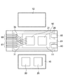
- FIG. 1 is a cross-sectional configuration diagram showing an example of a power module according to Embodiment 1 of the present invention.
- the power module according to the first embodiment includes a lower electrode 10, an intermediate electrode 11, an upper electrode 12, semiconductor switching elements 20 and 21, diodes 25 and 26, solder 30, a spacer 40, A signal line 61, bonding wires 70 and 71, and an electrode piece 81 are provided. Further, in FIG. 1, a mold resin 90 for performing resin sealing is indicated by a broken line.
- the semiconductor switching element 20 and the diode 25 are joined to the surface of the lower electrode 10 by the solder 30, and the spacer 40 is joined to the semiconductor switching element 20 and the diode 25 by the solder 30.
- the intermediate electrode 11 is also joined to the spacer 40 by the solder 30, and the semiconductor switching element 21 and the diode 26 are joined to the surface of the intermediate electrode 11 by the solder 30.
- a spacer 40 is joined to the semiconductor switching element 21 and the diode 26 by solder 30, and the upper electrode 12 is joined to the spacer 40 by solder 30.
- the lower electrode 10, the semiconductor switching element 20 and the diode 25, the intermediate electrode 11, the semiconductor switching element 13 and the diode 26, and the upper electrode 12 are arranged in this order via the spacer 40. It has a laminated structure. Since the solder 30 between the spacer 40 and the intermediate electrode 11 and the solder 30 between the spacer 40 and the upper electrode 12 are extremely thin, the solder between the spacer and the electrode is omitted in the drawings after FIG. And shall be illustrated.
- the signal line 61 and the electrode piece 81 are arranged on the same plane as the intermediate electrode 11.
- the semiconductor switching element 21 on the intermediate electrode 11 is connected to the signal line 61 by a bonding wire 71.
- the electrode piece 81 is provided so as to extend outward from the intermediate electrode 11.
- FIG. 2 is an exploded plan view of an example of the power module according to the first embodiment of the present invention, and corresponds to FIG. Therefore, the same reference numerals are given to the same components as those in FIG.
- the semiconductor switching element 20 and the diode 25 are provided on the surface of the lower electrode 10
- the semiconductor switching element 21 and the diode 26 are provided on the surface of the intermediate electrode 11. It is the same.
- a lead frame 50 is provided so as to surround the periphery of the intermediate electrode 11, the signal line 61 in addition to the signal line 60 on the left side of the lead frame 50, and the electrode pieces 80 and 82 in addition to the electrode piece 81 on the right side.
- a configuration in which is provided is newly shown.
- the signal line 60 is a signal line hidden behind the signal line 61 in FIG. 1, and the semiconductor switching element 20 on the surface of the lower electrode 10 is connected to the signal line 60. Further, the semiconductor switching element 21 on the surface of the intermediate electrode 11 is connected to the signal line 61 as shown in FIG.
- both the signal line 60 and the signal line 61 are arranged so as to extend outward on the same plane as the intermediate electrode 11.
- the semiconductor switching element 20 on the lower electrode 10 has a region that does not overlap with the intermediate electrode 11 in the stacking direction. That is, the semiconductor switching element 20 is in a state in which the left end portion of the semiconductor switching element 20 protrudes when viewed from above the intermediate electrode 11. Thereby, the semiconductor switching element 20 on the lower electrode 10 can be easily connected to the signal line 60 by the bonding wire 70 without being blocked by the intermediate electrode 11.
- an electrode piece 80 connected to the lower electrode 10 and an electrode piece 82 connected to the upper electrode 12 are arranged on both sides of the electrode piece 81.
- the electrode piece 81 is provided so as to extend to the right side from the intermediate electrode 11.
- the electrode piece 80 extends obliquely inward (center side) downward
- the electrode piece 82 extends obliquely inward (center side) upward
- the lower electrode 10 and the upper electrode 12 are placed under the intermediate electrode 11.
- the lower electrode 10 and the upper electrode 12 are in contact with each other. Details of this point will be described later.
- the intermediate electrode 11, the signal lines 60 and 61, and the electrode pieces 80, 81, and 82 are all composed of one lead frame 50. Accordingly, the intermediate electrode 11, the signal lines 60 and 61, the electrode pieces 80, 81, and 82 and the lead frame 50 can be configured by processing one metal plate, and the power module according to the first embodiment. Processing can be made extremely easy.
- the intermediate electrode 11 is made of a deformed material having a different thickness, but the lower electrode 10 and the upper electrode 12 are made of a plate-like plate material.
- the processing cost of the lower electrode 10 and the upper electrode 12 can be reduced, and the yield can be improved.
- the lower electrode 10 and the upper electrode 12 may be configured as the same electrode member having a congruent shape. Thereby, the lower electrode 10 and the upper electrode 12 can be formed using the same metal mold
- the lower electrode 10 and the upper electrode 12 may be formed in a simple shape, for example, may be configured in a rectangular shape. A plate-like member having a rectangular shape can be manufactured at a low cost, so that the yield can be further improved.
- the lower electrode 10 is an electrode disposed in the lower part, and is provided with a semiconductor switching element 20 and a diode 25 joined on the surface.
- the semiconductor switching element 20 and the diode 25 are joined to the surface of the lower electrode 10 with solder 30.
- the lower electrode 10, the semiconductor switching element 20, and the diode 25 are not only physically joined to the lower electrode 10 by the solder 30 but also electrically connected thereto.
- the semiconductor switching element 20 is an element for performing on / off switching by applying a voltage.
- an IGBT Insulated Gate Bipolar Transistor
- MOS Metal Oxide Semiconductor
- the diode 25 is a rectifying element provided in parallel with the semiconductor switching element 20.
- the signal line 60 is connected to a control terminal such as a gate of the semiconductor switching element 20, and on / off is controlled by an input from the signal line 60.
- a control terminal such as a gate of the semiconductor switching element 20 provided on the surface of the lower electrode 10
- the signal line 60 is provided on the same horizontal plane as the lower electrode 10.
- the intermediate electrode 81 is provided in the power module according to the present embodiment.
- the signal line 60 is disposed on the same horizontal plane as that shown in FIG. 1, and the signal line 60 and the bonding wire 70 are connected to each other.
- the spacer 40 functions to form an interval between the intermediate electrode 11 and the semiconductor switching element 20 and to electrically connect the intermediate electrode 11 and the semiconductor switching element 20. By forming a gap between the semiconductor switching element 20 and the intermediate electrode 11, heat generated in the semiconductor switching element 20 can be effectively released.
- the spacer 40 may be composed of, for example, a columnar metal block, and may be composed of, for example, a copper block.
- the spacer 40 on the diode 25 also forms a gap between the diode 25 and the intermediate electrode 11 and electrically connects the diode 25 and the intermediate electrode 11.
- the lower electrode 10 is connected to an electrode piece 80 provided on the same plane as the electrode piece 81, and power is supplied from the electrode piece 80.
- the intermediate electrode 11 is an electrode that serves as an output electrode of the semiconductor switching elements 20 and 21.
- the semiconductor switching element 21 on the surface of the intermediate electrode 11 is also electrically connected to the intermediate electrode 11 by solder bonding.
- the semiconductor switching element 21 is a switching element that is controlled to be turned on / off by application of a voltage. Like the semiconductor switching element 20, an IGBT or a MOS transistor may be used.
- the diode 26 is a rectifying element connected in parallel with the semiconductor switching element 21.
- a control terminal such as a gate of the semiconductor switching element 21 is connected to a signal line 61 and a bonding wire 71 which are on the same plane as the intermediate electrode 11.
- the electrode piece 81 extends horizontally from the intermediate electrode 11 and is connected to the outside to supply power to the semiconductor switching element 21 and the diode 26 on the intermediate electrode 11.
- the upper electrode 12 is an electrode that is stacked on and covers the semiconductor switching element 21 and the diode 26 via the spacer 40.
- the spacer 40 is a metal block and serves as a wiring, and thus electrically connects the semiconductor switching element 21 and the diode 26 to the upper electrode 12.
- a space is formed between the semiconductor switching element 21 and the diode 26 and the upper electrode 12 to play a role of promoting heat dissipation.
- the upper electrode 12 is connected to the electrode piece 82, and power is supplied from the electrode piece 82.
- the intermediate electrode 11, the semiconductor switching element 21 and the diode 26 constitute an upper arm, and the lower electrode 10.
- the semiconductor switching element 22 and the diode 25 constitute a lower arm.
- the power module according to the first embodiment has a configuration in which the semiconductor switching elements 20 and 21 are connected in series, and has a device stacking type small and high output configuration.
- FIG. 1 shows the power module in a state where the lead frame 50 has already been cut.
- FIG. 3 is a view for explaining an arrangement position of the intermediate electrode 11 of the power module according to the first embodiment of the present invention. Note that the overall configuration and individual components are substantially the same as those in FIG. 1, and thus the same reference numerals are given and description thereof is omitted.
- a part of the surface of the semiconductor switching element 20 has a region A that does not overlap the intermediate electrode 11. That is, the intermediate electrode 11 is arranged so as to avoid the signal pad provided on the semiconductor switching element 20. With this configuration, a free region A can be secured above the semiconductor switching element 20, and the lower semiconductor switching element 20 can be easily connected to the signal line 60 by bonding.
- the upper electrode 12 is disposed at a position overlapping the intermediate electrode 11, and secures a wire bonding space for the semiconductor switching element 20 together with the intermediate electrode 11.
- FIG. 4 is a configuration diagram illustrating an example of an electrode piece 82 connected to the upper electrode 12 of the power module according to the first embodiment of the present invention.
- the cross-sectional structure including the electrode piece 82 connected with the upper electrode 12 of the power module which concerns on a present Example is shown.
- the electrode piece 82 has a shape that opens from the center to the base so as to connect two parallel sides, and the upper surface of one end is connected to the lower surface of the right end portion of the upper electrode 12.
- the electrode piece 82 extends obliquely downward from the lower surface of the right end portion of the upper electrode 12 so as to open outward, and extends horizontally outward when it reaches the same plane as the intermediate electrode 11. Yes.
- a region B where the intermediate electrode 11 and the lower electrode 10 do not exist is secured below the connection point between the electrode piece 82 and the lower surface of the upper electrode 12.
- the electrode piece 82 is connected to the upper surface electrode 12 by dropping the solder 30 onto the joint portion of the electrode piece 82 from above with the upper electrode 12 positioned downward and the lower electrode 10 positioned upside down. Is called.
- a lower portion of the connection portion between the electrode piece 82 and the upper electrode 12 is provided.
- the intermediate electrode 11 and the lower electrode 10 that prevent the dripping of the solder 30 are not provided, and a space for connection work is secured.
- the electrode piece 82 is connected to the upper electrode 12 by providing the region B where the intermediate electrode 11 and the lower electrode 10 do not exist below the connection point between the upper electrode 12 and the electrode piece 82 as necessary. It is possible to secure a connection space for this purpose.
- the space of the region B is not essential and may be provided as necessary.
- the electrode piece 80 extending downward from the lead frame 50 on the same plane as the intermediate electrode 11 is joined to the lower electrode 10 at the same time when the lower electrode 10 and the intermediate electrode 11 are joined. There is no need to provide such a space.
- FIG. 5 is a diagram illustrating an example of a molding process of the power module according to the first embodiment of the present invention.
- FIG. 5 shows a state where the power module according to the first embodiment is clamped to a mold 100 for performing molding.
- the mold 100 includes an upper mold 102 and a lower mold 101, which are clamped together and filled with a mold resin 90 to be molded.
- the signal lines 60 and 61 and the electrode pieces 80 to 82 coincide with the parting line PL that is the boundary between the upper mold 102 and the lower mold 101.
- 61 and the electrode pieces 80 to 82 can be placed at the position of the parting line PL and clamped. That is, for example, if a mold that can accommodate the signal lines 60 and 61 is formed on the left side of the lower mold 101 and a mold that can accommodate the electrode pieces 80 to 82 is formed on the right side, the upper mold 102 and the lower mold 101 By clamping the mold, a mold for performing molding can be formed, and the molding can be easily performed. Thereby, the molding of the mold 100 becomes simple and easy, and the molding itself can be performed by a general process.
- the signal lines 60 and 61 and the electrode pieces 80 to 82 are all at the same height as the intermediate electrode 11 that coincides with the parting line PL of the mold 100.
- the shape of the mold 100 can be simplified and molding can be easily performed.
- the upper electrode 12 and the lower electrode 10 can be plate-like members, the yield can be greatly improved. Furthermore, when connecting the semiconductor switching elements 20 and 21 to the signal lines 60 and 61 by performing wire bonding, a connection space between the semiconductor switching element 20 and the signal line 60 on the surface of the lower electrode 10 is secured, Wire bonding can be performed easily. Furthermore, when the electrode piece 82 is connected to the upper electrode 12, a connection space is secured, so that the connection can be easily performed.
- FIG. 6A is a diagram showing a configuration of a conventional power module as a comparative example. 6A, the lower electrode 110, the semiconductor element 20 and the diode 25, the spacer 40, the intermediate electrode 111, the semiconductor switching element 21 and the diode 26, the spacer 40, and the upper electrode 112 are stacked in this order. Similar to the power module according to the example, but the signal lines 160 and 161 are on the same plane as the lower electrode 110 and the intermediate electrode 111, and the electrode pieces 180, 181 and 182 are on the same plane as the lower electrode 110, the intermediate electrode 111 and the upper electrode 112. This is different from the power module according to the present embodiment.
- the signal line 160 and the semiconductor switching element 20 on the lower electrode 110 are connected on the same plane by the bonding wire 170, and the signal line 161 and the semiconductor switching element 21 on the intermediate electrode 111 are connected. Connection is also made on the same plane by the bonding wire 171.
- both the lower electrode 110 and the intermediate electrode 111 are different in thickness from the signal lines 160 and 161 and the electrode pieces 180 and 181, and the whole is configured from a combination of deformed materials.
- the upper electrode 112 also has a different thickness from the electrode piece 182 and is composed of a combination of deformed materials having different thicknesses. Therefore, since the intermediate electrode 111 and the lower electrode 110 are configured to include portions having different thicknesses as a whole including the signal lines 160 and 161 and the electrode pieces 180 and 181, the structure becomes complicated. Thus, there is a problem that the processing yield is deteriorated and the cost for manufacturing the electrode member is increased.
- FIG. 6B is an exploded plan view showing a configuration of a conventional power module as a comparative example, and corresponds to FIG. 6A.
- all of the lower electrode 110, the intermediate electrode 111, and the upper electrode 112 have different shapes when including the electrode pieces 180, 181, and 182, and like the power module according to the present embodiment.
- FIG. 6C is a view showing a molding process of a conventional power module as a comparative example.
- a conventional power module is clamped to a mold 200 including an upper mold 202 and a lower mold 201.
- the right electrode pieces 180 to 182 can be molded by shifting the protruding positions of the electrode pieces 180 to 182 when viewed from above.
- the signal lines 160 and 161 are not on the same plane, and the signal lines 160 and 161 cannot be disposed so as to be sandwiched from above and below by the parting line PL. Processing is not possible and processing costs increase.
- the signal lines 60 and 61 and the electrode pieces 80 to 82 are all arranged on the same parting line PL and are sandwiched between the upper and lower sides. Since the mold can be clamped, mold molding can be easily performed. Moreover, since the upper electrode 12 and the lower electrode 10 can be comprised with a board
- the yield at the time of manufacture is maintained while maintaining a small and high output. It can be greatly improved.
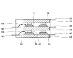
- FIG. 7 is a view showing an example of a power module according to the second embodiment of the present invention.
- the power module according to the second embodiment includes a lower electrode 10, an intermediate electrode 13, an upper electrode 14, semiconductor switching elements 20 and 21, and signal lines 60 and 61.
- FIG. 7 only the changed part of the first embodiment is shown, but the other components may include the same components as those of the first embodiment.
- the same components as those of the power module according to the first embodiment are denoted by the same reference numerals as those of the first embodiment, and the description thereof is omitted.
- the power module according to the second embodiment is different from the first embodiment in that the spacers 40 existing in the first embodiment are eliminated, and convex portions 41 are provided instead on the lower surface of the intermediate electrode 13 and the lower surface of the upper electrode 14. 1 is different from the power module according to 1.
- the electrodes can be used instead of the independent spacers 40.
- An integral convex portion 41 may be provided.
- FIG. 8 is a diagram showing the power module according to the first embodiment in the same format as FIG. As shown in FIG. 8, if the spacers 40 are provided independently, the number of parts increases.
- the configuration of the power module according to the second embodiment as shown in FIG. 7 or the configuration of the power module according to the first embodiment as shown in FIG. 8 is appropriately selected according to the use and the total cost. Can do.
- the convex part 41 in the upper part of the semiconductor switching elements 20 and 21 and the diodes 25 and 26 may make it provide as a convex shape of 1 mm or more, for example.
- the number of parts and the processing cost at the time of assembly can be reduced, and the cost can be reduced.
- FIG. 9 is a diagram showing a planar configuration of an intermediate electrode of an example of a power module according to Embodiment 3 of the present invention.
- the power module according to the third embodiment includes a lower electrode 15, an intermediate electrode 16, semiconductor switching elements 22 and 23, a diode 28, a lead frame 51, signal lines 62 and 63, and a bonding wire 72. , 73 and electrode pieces 83, 84, 85.
- the intermediate electrode 16, the signal lines 62 and 63, and the electrode pieces 83 to 84 are formed on the same lead frame 51 on the same plane.
- the power module according to the third embodiment three semiconductor switching elements 22 and 23 and three diodes 28 are provided on the lower electrode 15 and the intermediate electrode 16, respectively.
- the power module according to the first embodiment Is different.
- the power module according to the first embodiment is configured as a single-phase power module such as a single-phase inverter
- the power module according to the third embodiment is configured as a three-phase power module such as a three-phase inverter. An example will be described.
- Electrodes 23 and three diodes 28 are provided on the intermediate electrode 16 in correspondence with the U phase, the V phase, and the W phase. Accordingly, the electrode pieces 84 serving as the output electrodes of the respective phases are also provided so as to extend outward from the intermediate electrode 16 by three, corresponding to the three semiconductor switching elements 23 and the diodes 28. In FIG. 9, all three electrode pieces 84 are connected by one lead frame 51. However, after molding, the electrode pieces 84 are cut and electrically connected to each other. Insulated.
- the electrode piece 83 connected to the lower electrode 15 and the electrode piece 85 connected to the upper electrode may be shared by the three semiconductor switching elements 23 and the diodes 28. Yes, one each.
- the upper electrode 85 is shown with a portion extending toward the inner side (the signal lines 62 and 63 side), and this portion is connected to the upper electrode.
- the electrode piece 84 connected to the lower electrode 16 does not have such an inwardly extending portion, but actually has an inwardly extending portion below the intermediate electrode 16.
- the lower electrode 15 protrudes outward from the intermediate electrode 16, and the semiconductor switching element 22 on the lower electrode 15 has a portion that does not overlap with the intermediate electrode 16 on the outer side. Yes. Since the semiconductor switching element 22 on the lower electrode 15 has a portion that does not overlap the intermediate electrode 16 in the stacking direction, the semiconductor switching element 22 on the lower electrode 15 and the signal line 62 can be easily connected using the bonding wire 72. It can be carried out. Since three semiconductor switching elements 22 on the lower electrode 15 are also provided corresponding to three phases, the three semiconductor switching elements 22 are connected to the signal line 62 by wire bonding. In both cases, a connection space can be secured and wire bonding can be easily performed.
- the bonding can be easily performed using the bonding wire 73 by general wire bonding.
- the signal lines 62 and 63, the electrode pieces 83 to 85, and the intermediate electrode 16 are formed on the same lead frame 51 and are all on the same plane. Sometimes the parting line can be easily formed.
- FIG. 10 is an exploded perspective view showing an example of a power module according to the third embodiment. 10, the configuration of the intermediate electrode 16 corresponds to that in FIG. 9, so the same components are denoted by the same reference numerals as those in FIG. 9 and description thereof is omitted.
- three semiconductor switching elements 22 and three diodes 27 are joined and arranged on the surface of the lower electrode 15, and a spacer 42 is provided on each semiconductor switching element 22 and the diode 27.
- the intermediate electrode 16 is laminated thereon.
- Three semiconductor switching elements 23 and three diodes 28 are provided on the surface of the intermediate electrode 16, and the upper electrode 17 is laminated thereon via a spacer 42.
- the lower electrode 15 and the upper electrode 17 are also made of a plate material in the power module according to the third embodiment, and can be improved in yield.
- FIG. 11 is a cross-sectional configuration diagram illustrating an example of a power module according to the third embodiment.
- FIG. 11 shows a cross-sectional configuration in which the lower electrode 15, the semiconductor switching element 22 and the diode 27, the spacer 42, the intermediate electrode 16, the semiconductor switching element 23 and the diode 28, and the upper electrode 17 are laminated in this order from the bottom.
- an electrode piece 84 extends horizontally to the outside on the right side, and on the opposite side, a signal line 62 extends horizontally to the outside on the left side.
- the semiconductor switching elements 22 are connected by bonding wires 72 from below, and the semiconductor switching elements 23 on the intermediate electrode 16 are connected by bonding wires 73 to signal lines 63 (not shown in FIG. 11).
- the semiconductor switching element 22 Since the semiconductor switching element 22 has a portion that does not overlap the intermediate electrode 16 in the stacking direction and protrudes to the signal line 62 side from the intermediate electrode 16, a connection space by the bonding wire 72 can be secured and wire bonding can be easily performed. It can be carried out.
- the electrode piece 85 is not shown in FIG. 11, there is a space below the upper electrode 17 that does not overlap the intermediate electrode 16 and the lower electrode 15, and the upper electrode 17 can be easily joined to the electrode piece 85. It has a configuration.
- the side surfaces of the lower electrode 15, the intermediate electrode 16, and the upper electrode 17 are molded with the mold resin 90, and the signal lines 62 and the outer sides of the electrode pieces 84 protrude from the mold resin 90 and are exposed. Since the signal line 62 and the electrode piece 84 are on the same plane, and the signal line 63 and the electrode pieces 83 and 85 (not shown) are also on the same plane, the configuration of the parting line at the time of molding is facilitated. It has a configuration that can. Further, since the signal lines 62 and 63 and the electrode pieces 83 to 85 are arranged on the opposite side via the intermediate electrode 16, the signal lines 62 and 63 and the electrode pieces 83 to 85 which are power lines are separated from each other. The structure is such that noise is unlikely to occur.
- the lower surface of the lower electrode 15 and the upper surface of the upper electrode 17 are exposed without being sealed with resin, and the cooling efficiency can be increased.
- the cooling efficiency of the power module can be increased.
- FIG. 12A is a perspective view illustrating a completed state of the power module according to the third embodiment.
- FIG. 12A shows a state in which the electrode pieces 83 to 85 are disposed on the front side, the signal lines 62 and 63 are disposed on the back side, and the semiconductor switching element 23 and the diode 28 are disposed on the center.
- Three electrode pieces 84 are provided so as to protrude for three-phase output, and the electrode piece 85 for the upper electrode 17 and the electrode piece 83 for the lower electrode 15 can be shared by the three phases.
- One by one is provided.
- the signal lines 62 and 63 are configured such that the signal line 62 for the semiconductor switching element 22 on the lower electrode 15 and the signal line 63 for the semiconductor switching element 23 on the intermediate electrode 16 are provided on the same plane. It has become.
- FIG. 12B is a perspective view showing the power module according to the third embodiment shown in FIG. 12A from the opposite side.
- the signal lines 62 and 63 are shown on the front side.
- the wire bonding of the semiconductor switching element 23 and the signal line 63 on the same plane using the bonding wire 73, and the lower part using the bonding wire 72. It is shown that the wire bonding of the semiconductor switching element 22 and the signal line 62 on the electrode 15 is performed alternately.
- the power module according to the third embodiment even in a three-phase power module, molding can be facilitated, the electrode shape can be simplified, and the yield can be improved.
- FIGS. 13A to 13E are diagrams illustrating a series of steps of an example of a method for manufacturing a power module according to the third embodiment.
- the same referential mark is attached
- FIG. 13A is a front view illustrating an example of a semiconductor switching element bonding step in the method for manufacturing a power module according to the third embodiment.
- the semiconductor switching element bonding step the semiconductor switching elements 22 and 23 are bonded onto the lower electrode 15 and the intermediate electrode 16, respectively. Specifically, the semiconductor switching element 22 is joined to the surface of the lower electrode 15 by soldering using the solder 31. Further, the semiconductor switching element 23 is joined to the surface of the intermediate electrode 16 by soldering using the solder 31.
- the spacer 42 is bonded to the semiconductor switching elements 22 and 23 by soldering using the solder 31 in addition to the semiconductor switching elements 22 and 23.
- FIG. 13A As shown in FIG. 9, since the lower electrode 15 is a single plate-like electrode, three semiconductor switching elements 22 are joined on the surface of the plate-like lower electrode 15. .
- the intermediate electrode 16 since the intermediate electrode 16 has a shape separated for each junction region of the semiconductor switching element 23 of each phase, it corresponds to FIG. 13A and is separated and arranged for each semiconductor switching element 23 on the intermediate electrode 16. ing.
- the upper and lower arms of the power module are completed by the semiconductor switching element joining process.
- the upper arm is the plus side and the lower arm is the minus side
- the lower electrode 15 and the semiconductor switching element 22 bonded on the surface thereof are connected to the upper arm U, the intermediate electrode 16 and the surface thereof.
- the semiconductor switching element 23 bonded to the lower arm L will be described.
- FIG. 13B is a front view showing an example of the upper arm / lower arm joining step of the power module manufacturing method according to the third embodiment.
- the upper arm U and the lower arm L are solder-joined.
- a lower arm L having an intermediate electrode 16 and a semiconductor switching element 23 is soldered by a solder 31 on an upper arm U having a lower electrode 15 and a semiconductor switching element 22.
- FIG. 13C is a side view showing an example of the wire bonding step of the method for manufacturing the power module according to the third embodiment.
- 13A and 13B are front views, but FIG. 13C is a side view so that the connection relationship in the wire bonding process can be understood.
- the semiconductor switching elements 22 and 23 and the signal lines 62 and 63 are joined using the bonding wires 72 and 73.
- the semiconductor switching element 22 on the surface of the lower electrode 15 has a step with the signal line 62 on the same plane as the intermediate electrode 16, but has a portion that is not covered by the intermediate electrode 16.
- a connection space for arranging the bonding wires 72 can be secured.
- the semiconductor switching element 23 on the intermediate electrode 16 is connected to the signal line 63 on the same plane.
- the wire which consists of various materials may be used for the bonding wires 72 and 73 according to a use, you may use an aluminum wire, for example.
- electrode pieces 83 to 85 are provided on the side opposite to the signal lines 62 and 63, but the connection between the electrode piece 83 and the lower electrode 15 is simultaneously performed at this stage.
- the joining of the electrode pieces 83 may also be solder joining using the solder 31.
- FIG. 13D is a front view showing an example of the upper electrode joining step of the power module manufacturing method according to the third embodiment.
- the upper electrode bonding step the upper electrode 17 is bonded to the upper portion of the semiconductor switching element 23 on the intermediate electrode 16.
- the joining may be performed by solder joining using the solder 31.
- solder bonding between the upper electrode 17 and the electrode piece 85 is also performed.
- the electrical connection of the stacked power module is completed by the upper electrode joining step.
- FIG. 13E is a front view showing an example of a molding process of the power module manufacturing process according to the third embodiment.
- the portions other than the upper surface of the upper electrode 17 and the lower surface of the lower electrode 15 are sealed with mold resin.
- the parting line of the mold has only to clamp the signal lines 62 and 63 and the electrode pieces 83 to 85 on the same plane. Can be configured.
- the electrode configuration can be simplified and the yield can be improved.
- a cooling fin may be provided on the upper surface of the upper electrode 17 and / or the lower surface of the lower electrode 15 to increase the cooling efficiency of the power module. Since the lower electrode 15 and the upper electrode 17 are simple plate materials, the process of providing fins can be easily performed.
- cooling fins are provided on the upper surface of the upper electrode 17 and / or the lower surface of the lower electrode 15 can also be applied to the power modules according to the first and second embodiments.
- the present invention can be applied to a power module using an IGBT, a power MOS transistor, or the like as a semiconductor switching element.
Landscapes
- Engineering & Computer Science (AREA)
- Computer Hardware Design (AREA)
- Microelectronics & Electronic Packaging (AREA)
- Power Engineering (AREA)
- Physics & Mathematics (AREA)
- Condensed Matter Physics & Semiconductors (AREA)
- General Physics & Mathematics (AREA)
- Manufacturing & Machinery (AREA)
- Inverter Devices (AREA)
- Thyristors (AREA)
Abstract
Description
前記第1乃至第3の電極とそれぞれ電気的に接続される第1乃至第3の電極片と、
前記第1及び第2のスイッチング素子とそれぞれ電気的に接続される第1及び第2の信号線とを有し、
前記第1乃至第3の電極片と前記第1及び第2の信号線は、前記第2の電極と同一平面上で外側に延びて設けられたことを特徴とする。
11、13、16 中間電極
12、14、17 上部電極
20、21、22、23 半導体スイッチング素子
25、26、27、28 ダイオード
30、31 はんだ
40、41、42 スペーサ
50、51 リードフレーム
60、61、62、63 信号線
70、71、72、73 ボンディングワイヤ
80、81、82、83、84、85 電極片
90、91 モールド樹脂
100、101、102 金型
Claims (10)
- 表面上に第1のスイッチング素子が接合された第1の電極と、表面上に第2のスイッチング素子が接合された第2の電極と、第3の電極とを、前記第1の電極、前記第1のスイッチング素子、前記第2の電極、前記第2のスイッチング素子及び前記第3の電極の順に積層方向に配置したパワーモジュールにおいて、
前記第1乃至第3の電極とそれぞれ電気的に接続される第1乃至第3の電極片と、
前記第1及び第2のスイッチング素子とそれぞれ電気的に接続される第1及び第2の信号線とを有し、
前記第1乃至第3の電極片と前記第1及び第2の信号線は、前記第2の電極と同一平面上で外側に延びて設けられたことを特徴とするパワーモジュール。 - 前記第1のスイッチング素子は、前記第2の電極と積層方向に重ならない領域を有することを特徴とする請求項1に記載のパワーモジュール。
- 前記第2の電極と、前記第1乃至第3の電極片と、前記第1及び第2の信号線とが、同一のリードフレーム上に構成されていることを特徴とする請求項2に記載のパワーモジュール。
- 前記第3の電極片の接合部が、前記第1及び第2の電極片と積層方向に重ならない領域を有することを特徴とする請求項3に記載のパワーモジュール。
- 前記第1乃至第3の電極片と、前記第1及び第2の信号線とは、前記第2の電極を介して反対側に設けられたことを特徴とする請求項4に記載のパワーモジュール。
- 前記第1及び第2の信号線は、ワイヤボンディングにより前記第1及び第2のスイッチング素子に接続されたことを特徴とする請求項5に記載のパワーモジュール。
- 前記第1及び第2の電極は、合同な形状を有することを特徴とする請求項6に記載のパワーモジュール。
- 前記第1及び第2の電極は、長方形形状であることを特徴とする請求項7に記載のパワーモジュール。
- 前記第1のスイッチング素子と前記第2の電極、及び前記第2のスイッチング素子と前記第3の電極は、金属ブロックからなるスペーサを介して積層されていることを特徴とする請求項8に記載のパワーモジュール。
- 前記第1乃至第3の電極片及び前記第1及び第2の信号線の外側部分のみが露出するように、前記第1乃至第3の電極、前記第1乃至第3の電極片及び前記第1及び第2の信号線がモールド成形により樹脂封止されたことを特徴とする請求項9に記載のパワーモジュール。
Priority Applications (5)
| Application Number | Priority Date | Filing Date | Title |
|---|---|---|---|
| PCT/JP2011/061239 WO2012157069A1 (ja) | 2011-05-16 | 2011-05-16 | パワーモジュール |
| US14/117,165 US8878347B2 (en) | 2011-05-16 | 2011-05-16 | Power module |
| JP2013514907A JP5895933B2 (ja) | 2011-05-16 | 2011-05-16 | パワーモジュール |
| DE112011105247.2T DE112011105247B4 (de) | 2011-05-16 | 2011-05-16 | Leistungsmodul |
| CN201180070873.4A CN103534805B (zh) | 2011-05-16 | 2011-05-16 | 功率模块 |
Applications Claiming Priority (1)
| Application Number | Priority Date | Filing Date | Title |
|---|---|---|---|
| PCT/JP2011/061239 WO2012157069A1 (ja) | 2011-05-16 | 2011-05-16 | パワーモジュール |
Publications (1)
| Publication Number | Publication Date |
|---|---|
| WO2012157069A1 true WO2012157069A1 (ja) | 2012-11-22 |
Family
ID=47176437
Family Applications (1)
| Application Number | Title | Priority Date | Filing Date |
|---|---|---|---|
| PCT/JP2011/061239 WO2012157069A1 (ja) | 2011-05-16 | 2011-05-16 | パワーモジュール |
Country Status (5)
| Country | Link |
|---|---|
| US (1) | US8878347B2 (ja) |
| JP (1) | JP5895933B2 (ja) |
| CN (1) | CN103534805B (ja) |
| DE (1) | DE112011105247B4 (ja) |
| WO (1) | WO2012157069A1 (ja) |
Cited By (9)
| Publication number | Priority date | Publication date | Assignee | Title |
|---|---|---|---|---|
| JP2014130894A (ja) * | 2012-12-28 | 2014-07-10 | Toyota Motor Corp | 半導体モジュール |
| JP5657816B1 (ja) * | 2013-02-28 | 2015-01-21 | 新電元工業株式会社 | モジュール、モジュール組合体及びモジュールの製造方法 |
| WO2015053002A1 (ja) * | 2013-10-07 | 2015-04-16 | トヨタ自動車株式会社 | 半導体モジュール |
| WO2016125674A1 (ja) * | 2015-02-02 | 2016-08-11 | 株式会社村田製作所 | 半導体モジュールおよび半導体モジュールの製造方法 |
| KR101766082B1 (ko) * | 2015-12-09 | 2017-08-07 | 현대자동차주식회사 | 파워모듈 |
| WO2018211684A1 (ja) * | 2017-05-19 | 2018-11-22 | 新電元工業株式会社 | 電子モジュール、リードフレーム及び電子モジュールの製造方法 |
| WO2018211680A1 (ja) * | 2017-05-19 | 2018-11-22 | 新電元工業株式会社 | 電子モジュール |
| KR20190065768A (ko) * | 2017-12-04 | 2019-06-12 | 현대자동차주식회사 | 적층 구조를 이용한 파워모듈 및 이를 이용한 전기자동차용 3상 구동 모듈 |
| WO2023090072A1 (ja) * | 2021-11-16 | 2023-05-25 | ローム株式会社 | 半導体装置 |
Families Citing this family (19)
| Publication number | Priority date | Publication date | Assignee | Title |
|---|---|---|---|---|
| US8987876B2 (en) * | 2013-03-14 | 2015-03-24 | General Electric Company | Power overlay structure and method of making same |
| US11570921B2 (en) * | 2015-06-11 | 2023-01-31 | Tesla, Inc. | Semiconductor device with stacked terminals |
| US10388539B2 (en) | 2015-07-24 | 2019-08-20 | Semiconductor Components Industries, Llc | Semiconductor component and method of manufacture |
| US9818674B2 (en) | 2015-07-24 | 2017-11-14 | Semiconductor Components Industries, Llc | Semiconductor component and method of manufacture |
| US9818677B2 (en) | 2015-07-24 | 2017-11-14 | Semiconductor Components Industries, Llc | Semiconductor component having group III nitride semiconductor device mounted on substrate and interconnected to lead frame |
| US9653387B2 (en) | 2015-07-24 | 2017-05-16 | Semiconductor Components Industries, Llc | Semiconductor component and method of manufacture |
| US10128174B2 (en) | 2015-07-24 | 2018-11-13 | Semiconductor Components Industries, Llc | Semiconductor component and method of manufacture |
| US9735095B2 (en) | 2015-07-24 | 2017-08-15 | Semiconductor Components Industries, Llc | Semiconductor component and method of manufacture |
| US9780019B2 (en) | 2015-07-24 | 2017-10-03 | Semiconductor Components Industries, Llc | Semiconductor component and method of manufacture |
| US9620443B2 (en) * | 2015-07-24 | 2017-04-11 | Semiconductor Components Industries, Llc | Semiconductor component and method of manufacture |
| US9905500B2 (en) | 2015-07-24 | 2018-02-27 | Semiconductor Components Industries, Llc | Semiconductor component and method of manufacture |
| DE102016101433A1 (de) * | 2016-01-27 | 2017-07-27 | Infineon Technologies Ag | Multi-Chip-Halbleiterleistungsgehäuse |
| US9972559B2 (en) | 2016-05-19 | 2018-05-15 | Hyundai Motor Company | Signal block and double-faced cooling power module using the same |
| JP6772768B2 (ja) * | 2016-11-09 | 2020-10-21 | 株式会社デンソー | 半導体装置 |
| JP2018101664A (ja) * | 2016-12-19 | 2018-06-28 | トヨタ自動車株式会社 | 半導体装置の製造方法 |
| US11437298B2 (en) | 2017-09-14 | 2022-09-06 | Shindengen Electric Manufacturing Co., Ltd. | Electronic module and method for manufacturing electronic module |
| JP7077893B2 (ja) * | 2018-09-21 | 2022-05-31 | 株式会社デンソー | 半導体装置 |
| FR3092698B1 (fr) * | 2019-02-11 | 2021-05-07 | St Microelectronics Tours Sas | Assemblage comportant un composant vertical de puissance monté sur une plaque métallique de connexion |
| CN112701095B (zh) * | 2020-12-15 | 2022-10-14 | 杰群电子科技(东莞)有限公司 | 一种功率芯片堆叠封装结构 |
Citations (2)
| Publication number | Priority date | Publication date | Assignee | Title |
|---|---|---|---|---|
| JP2006134990A (ja) * | 2004-11-04 | 2006-05-25 | Fuji Electric Holdings Co Ltd | 半導体装置 |
| JP2009295794A (ja) * | 2008-06-05 | 2009-12-17 | Mitsubishi Electric Corp | 樹脂封止型半導体装置とその製造方法 |
Family Cites Families (10)
| Publication number | Priority date | Publication date | Assignee | Title |
|---|---|---|---|---|
| JP4192396B2 (ja) | 2000-04-19 | 2008-12-10 | 株式会社デンソー | 半導体スイッチングモジュ−ル及びそれを用いた半導体装置 |
| JP4409064B2 (ja) | 2000-07-14 | 2010-02-03 | 三菱電機株式会社 | パワー素子を含む半導体装置 |
| JP4110992B2 (ja) * | 2003-02-07 | 2008-07-02 | セイコーエプソン株式会社 | 半導体装置、電子デバイス、電子機器、半導体装置の製造方法および電子デバイスの製造方法 |
| JP4438489B2 (ja) | 2004-04-13 | 2010-03-24 | 富士電機システムズ株式会社 | 半導体装置 |
| JP2006049542A (ja) | 2004-08-04 | 2006-02-16 | Toyota Motor Corp | パワーモジュール |
| JP2006216940A (ja) | 2005-01-07 | 2006-08-17 | Toshiba Corp | 半導体装置 |
| JP4629016B2 (ja) * | 2006-10-27 | 2011-02-09 | 三菱マテリアル株式会社 | ヒートシンク付パワーモジュール用基板およびヒートシンク付パワーモジュール用基板の製造方法並びにパワーモジュール |
| JP2008218688A (ja) * | 2007-03-05 | 2008-09-18 | Denso Corp | 半導体装置 |
| JP4900148B2 (ja) | 2007-09-13 | 2012-03-21 | 三菱電機株式会社 | 半導体装置 |
| JP5947537B2 (ja) * | 2011-04-19 | 2016-07-06 | トヨタ自動車株式会社 | 半導体装置及びその製造方法 |
-
2011
- 2011-05-16 DE DE112011105247.2T patent/DE112011105247B4/de not_active Expired - Fee Related
- 2011-05-16 US US14/117,165 patent/US8878347B2/en active Active
- 2011-05-16 WO PCT/JP2011/061239 patent/WO2012157069A1/ja active Application Filing
- 2011-05-16 CN CN201180070873.4A patent/CN103534805B/zh not_active Expired - Fee Related
- 2011-05-16 JP JP2013514907A patent/JP5895933B2/ja active Active
Patent Citations (2)
| Publication number | Priority date | Publication date | Assignee | Title |
|---|---|---|---|---|
| JP2006134990A (ja) * | 2004-11-04 | 2006-05-25 | Fuji Electric Holdings Co Ltd | 半導体装置 |
| JP2009295794A (ja) * | 2008-06-05 | 2009-12-17 | Mitsubishi Electric Corp | 樹脂封止型半導体装置とその製造方法 |
Cited By (17)
| Publication number | Priority date | Publication date | Assignee | Title |
|---|---|---|---|---|
| JP2014130894A (ja) * | 2012-12-28 | 2014-07-10 | Toyota Motor Corp | 半導体モジュール |
| JP5657816B1 (ja) * | 2013-02-28 | 2015-01-21 | 新電元工業株式会社 | モジュール、モジュール組合体及びモジュールの製造方法 |
| WO2015053002A1 (ja) * | 2013-10-07 | 2015-04-16 | トヨタ自動車株式会社 | 半導体モジュール |
| JP2015076440A (ja) * | 2013-10-07 | 2015-04-20 | トヨタ自動車株式会社 | 半導体モジュール |
| CN105612616A (zh) * | 2013-10-07 | 2016-05-25 | 丰田自动车株式会社 | 半导体模块 |
| WO2016125674A1 (ja) * | 2015-02-02 | 2016-08-11 | 株式会社村田製作所 | 半導体モジュールおよび半導体モジュールの製造方法 |
| JPWO2016125674A1 (ja) * | 2015-02-02 | 2017-10-12 | 株式会社村田製作所 | 半導体モジュールおよび半導体モジュールの製造方法 |
| KR101766082B1 (ko) * | 2015-12-09 | 2017-08-07 | 현대자동차주식회사 | 파워모듈 |
| WO2018211684A1 (ja) * | 2017-05-19 | 2018-11-22 | 新電元工業株式会社 | 電子モジュール、リードフレーム及び電子モジュールの製造方法 |
| WO2018211680A1 (ja) * | 2017-05-19 | 2018-11-22 | 新電元工業株式会社 | 電子モジュール |
| JP6463558B1 (ja) * | 2017-05-19 | 2019-02-06 | 新電元工業株式会社 | 電子モジュール、リードフレーム及び電子モジュールの製造方法 |
| TWI683373B (zh) * | 2017-05-19 | 2020-01-21 | 日商新電元工業股份有限公司 | 電子模組 |
| US11037870B2 (en) | 2017-05-19 | 2021-06-15 | Shindengen Electric Manufacturing Co., Ltd. | Electronic module, lead frame and manufacturing method for electronic module |
| US11189591B2 (en) | 2017-05-19 | 2021-11-30 | Shindengen Electric Manufacturing Co., Ltd. | Electronic module |
| KR20190065768A (ko) * | 2017-12-04 | 2019-06-12 | 현대자동차주식회사 | 적층 구조를 이용한 파워모듈 및 이를 이용한 전기자동차용 3상 구동 모듈 |
| KR102474608B1 (ko) * | 2017-12-04 | 2022-12-06 | 현대자동차주식회사 | 적층 구조를 이용한 파워모듈 및 이를 이용한 전기자동차용 3상 구동 모듈 |
| WO2023090072A1 (ja) * | 2021-11-16 | 2023-05-25 | ローム株式会社 | 半導体装置 |
Also Published As
| Publication number | Publication date |
|---|---|
| US8878347B2 (en) | 2014-11-04 |
| CN103534805B (zh) | 2016-08-24 |
| JPWO2012157069A1 (ja) | 2014-07-31 |
| US20140197525A1 (en) | 2014-07-17 |
| DE112011105247T5 (de) | 2014-02-13 |
| CN103534805A (zh) | 2014-01-22 |
| DE112011105247B4 (de) | 2019-07-18 |
| JP5895933B2 (ja) | 2016-03-30 |
Similar Documents
| Publication | Publication Date | Title |
|---|---|---|
| JP5895933B2 (ja) | パワーモジュール | |
| JP5947537B2 (ja) | 半導体装置及びその製造方法 | |
| JP5971263B2 (ja) | 半導体装置 | |
| JP6750514B2 (ja) | 半導体装置 | |
| WO2013146212A1 (ja) | 半導体装置及び半導体装置の製造方法 | |
| JP6319137B2 (ja) | 半導体装置及びその製造方法 | |
| JP6119825B2 (ja) | パワーモジュール | |
| JP4885046B2 (ja) | 電力用半導体モジュール | |
| JP5811072B2 (ja) | パワーモジュール | |
| JP2019212833A (ja) | 半導体装置およびその製造方法 | |
| JP2006186170A (ja) | 半導体装置 | |
| JP5668707B2 (ja) | 半導体モジュール | |
| JP2012074730A (ja) | 電力用半導体モジュール | |
| WO2020208739A1 (ja) | 半導体装置 | |
| JP5869285B2 (ja) | 半導体装置 | |
| JP4910889B2 (ja) | 半導体装置 | |
| JP2013125889A (ja) | 半導体装置 | |
| JP6785893B2 (ja) | パワーモジュール及びその製造方法 | |
| JP2019029410A (ja) | 半導体モジュール | |
| JP2018093616A (ja) | 半導体装置 | |
| JP2016076727A (ja) | 半導体装置 | |
| JP5891744B2 (ja) | 半導体装置 | |
| JP5800716B2 (ja) | 電力用半導体装置 | |
| US10903138B2 (en) | Semiconductor device and method of manufacturing the same | |
| JP2014154770A (ja) | 半導体装置、及び、半導体装置の製造方法 |
Legal Events
| Date | Code | Title | Description |
|---|---|---|---|
| 121 | Ep: the epo has been informed by wipo that ep was designated in this application |
Ref document number: 11865477 Country of ref document: EP Kind code of ref document: A1 |
|
| ENP | Entry into the national phase |
Ref document number: 2013514907 Country of ref document: JP Kind code of ref document: A |
|
| WWE | Wipo information: entry into national phase |
Ref document number: 14117165 Country of ref document: US |
|
| WWE | Wipo information: entry into national phase |
Ref document number: 1120111052472 Country of ref document: DE Ref document number: 112011105247 Country of ref document: DE |
|
| 122 | Ep: pct application non-entry in european phase |
Ref document number: 11865477 Country of ref document: EP Kind code of ref document: A1 |