WO2015041157A1 - 有機エレクトロルミネッセンス素子 - Google Patents
有機エレクトロルミネッセンス素子 Download PDFInfo
- Publication number
- WO2015041157A1 WO2015041157A1 PCT/JP2014/074174 JP2014074174W WO2015041157A1 WO 2015041157 A1 WO2015041157 A1 WO 2015041157A1 JP 2014074174 W JP2014074174 W JP 2014074174W WO 2015041157 A1 WO2015041157 A1 WO 2015041157A1
- Authority
- WO
- WIPO (PCT)
- Prior art keywords
- compound
- layer
- light emitting
- group
- organic electroluminescence
- Prior art date
Links
- 238000005401 electroluminescence Methods 0.000 title claims abstract description 67
- 239000010410 layer Substances 0.000 claims abstract description 302
- 150000001875 compounds Chemical class 0.000 claims abstract description 184
- 230000003111 delayed effect Effects 0.000 claims abstract description 81
- 239000012044 organic layer Substances 0.000 claims abstract description 20
- 230000000903 blocking effect Effects 0.000 claims description 84
- 239000000463 material Substances 0.000 claims description 81
- 238000012546 transfer Methods 0.000 claims description 16
- 230000005281 excited state Effects 0.000 abstract description 12
- 239000010408 film Substances 0.000 description 38
- 125000003545 alkoxy group Chemical group 0.000 description 31
- 125000000217 alkyl group Chemical group 0.000 description 27
- 125000005647 linker group Chemical group 0.000 description 20
- 238000006467 substitution reaction Methods 0.000 description 20
- 230000005525 hole transport Effects 0.000 description 19
- 238000002347 injection Methods 0.000 description 19
- 239000007924 injection Substances 0.000 description 19
- YXFVVABEGXRONW-UHFFFAOYSA-N Toluene Chemical compound CC1=CC=CC=C1 YXFVVABEGXRONW-UHFFFAOYSA-N 0.000 description 18
- 125000004432 carbon atom Chemical group C* 0.000 description 18
- 125000003118 aryl group Chemical group 0.000 description 17
- 239000000203 mixture Substances 0.000 description 17
- 238000007740 vapor deposition Methods 0.000 description 17
- 125000001997 phenyl group Chemical group [H]C1=C([H])C([H])=C(*)C([H])=C1[H] 0.000 description 16
- 239000000758 substrate Substances 0.000 description 15
- 230000005284 excitation Effects 0.000 description 12
- 238000000034 method Methods 0.000 description 12
- 238000006862 quantum yield reaction Methods 0.000 description 11
- 229910052782 aluminium Inorganic materials 0.000 description 10
- XAGFODPZIPBFFR-UHFFFAOYSA-N aluminium Chemical compound [Al] XAGFODPZIPBFFR-UHFFFAOYSA-N 0.000 description 10
- 238000000295 emission spectrum Methods 0.000 description 10
- 125000001424 substituent group Chemical group 0.000 description 10
- 125000002947 alkylene group Chemical group 0.000 description 9
- 230000006798 recombination Effects 0.000 description 9
- 238000005215 recombination Methods 0.000 description 9
- FYYHWMGAXLPEAU-UHFFFAOYSA-N Magnesium Chemical compound [Mg] FYYHWMGAXLPEAU-UHFFFAOYSA-N 0.000 description 8
- 125000004450 alkenylene group Chemical group 0.000 description 8
- 239000011521 glass Substances 0.000 description 8
- 239000011777 magnesium Substances 0.000 description 8
- 229910052749 magnesium Inorganic materials 0.000 description 8
- -1 phenyloxy Group Chemical group 0.000 description 8
- 125000004076 pyridyl group Chemical group 0.000 description 8
- 125000004104 aryloxy group Chemical group 0.000 description 7
- 229940126214 compound 3 Drugs 0.000 description 7
- 239000007772 electrode material Substances 0.000 description 7
- 125000004435 hydrogen atom Chemical group [H]* 0.000 description 7
- 230000007246 mechanism Effects 0.000 description 7
- 229910052751 metal Inorganic materials 0.000 description 7
- 239000002184 metal Substances 0.000 description 7
- 125000000732 arylene group Chemical group 0.000 description 6
- 230000000052 comparative effect Effects 0.000 description 6
- 238000005259 measurement Methods 0.000 description 6
- 239000000243 solution Substances 0.000 description 6
- 229910052799 carbon Inorganic materials 0.000 description 5
- 238000002189 fluorescence spectrum Methods 0.000 description 5
- 150000002894 organic compounds Chemical class 0.000 description 5
- VFUDMQLBKNMONU-UHFFFAOYSA-N 9-[4-(4-carbazol-9-ylphenyl)phenyl]carbazole Chemical compound C12=CC=CC=C2C2=CC=CC=C2N1C1=CC=C(C=2C=CC(=CC=2)N2C3=CC=CC=C3C3=CC=CC=C32)C=C1 VFUDMQLBKNMONU-UHFFFAOYSA-N 0.000 description 4
- 238000000862 absorption spectrum Methods 0.000 description 4
- 125000002029 aromatic hydrocarbon group Chemical group 0.000 description 4
- 125000004429 atom Chemical group 0.000 description 4
- 238000006243 chemical reaction Methods 0.000 description 4
- 125000004122 cyclic group Chemical group 0.000 description 4
- AMGQUBHHOARCQH-UHFFFAOYSA-N indium;oxotin Chemical compound [In].[Sn]=O AMGQUBHHOARCQH-UHFFFAOYSA-N 0.000 description 4
- GHYOCDFICYLMRF-UTIIJYGPSA-N (2S,3R)-N-[(2S)-3-(cyclopenten-1-yl)-1-[(2R)-2-methyloxiran-2-yl]-1-oxopropan-2-yl]-3-hydroxy-3-(4-methoxyphenyl)-2-[[(2S)-2-[(2-morpholin-4-ylacetyl)amino]propanoyl]amino]propanamide Chemical compound C1(=CCCC1)C[C@@H](C(=O)[C@@]1(OC1)C)NC([C@H]([C@@H](C1=CC=C(C=C1)OC)O)NC([C@H](C)NC(CN1CCOCC1)=O)=O)=O GHYOCDFICYLMRF-UTIIJYGPSA-N 0.000 description 3
- 125000001989 1,3-phenylene group Chemical group [H]C1=C([H])C([*:1])=C([H])C([*:2])=C1[H] 0.000 description 3
- WHXSMMKQMYFTQS-UHFFFAOYSA-N Lithium Chemical compound [Li] WHXSMMKQMYFTQS-UHFFFAOYSA-N 0.000 description 3
- 125000004419 alkynylene group Chemical group 0.000 description 3
- 230000004888 barrier function Effects 0.000 description 3
- 229940125904 compound 1 Drugs 0.000 description 3
- 229940125797 compound 12 Drugs 0.000 description 3
- 239000000470 constituent Substances 0.000 description 3
- 230000005283 ground state Effects 0.000 description 3
- 238000004770 highest occupied molecular orbital Methods 0.000 description 3
- 229910052738 indium Inorganic materials 0.000 description 3
- APFVFJFRJDLVQX-UHFFFAOYSA-N indium atom Chemical compound [In] APFVFJFRJDLVQX-UHFFFAOYSA-N 0.000 description 3
- 229910052744 lithium Inorganic materials 0.000 description 3
- PQXKHYXIUOZZFA-UHFFFAOYSA-M lithium fluoride Chemical compound [Li+].[F-] PQXKHYXIUOZZFA-UHFFFAOYSA-M 0.000 description 3
- 238000004768 lowest unoccupied molecular orbital Methods 0.000 description 3
- 150000004866 oxadiazoles Chemical class 0.000 description 3
- 238000001296 phosphorescence spectrum Methods 0.000 description 3
- 238000004544 sputter deposition Methods 0.000 description 3
- QFLWZFQWSBQYPS-AWRAUJHKSA-N (3S)-3-[[(2S)-2-[[(2S)-2-[5-[(3aS,6aR)-2-oxo-1,3,3a,4,6,6a-hexahydrothieno[3,4-d]imidazol-4-yl]pentanoylamino]-3-methylbutanoyl]amino]-3-(4-hydroxyphenyl)propanoyl]amino]-4-[1-bis(4-chlorophenoxy)phosphorylbutylamino]-4-oxobutanoic acid Chemical compound CCCC(NC(=O)[C@H](CC(O)=O)NC(=O)[C@H](Cc1ccc(O)cc1)NC(=O)[C@@H](NC(=O)CCCCC1SC[C@@H]2NC(=O)N[C@H]12)C(C)C)P(=O)(Oc1ccc(Cl)cc1)Oc1ccc(Cl)cc1 QFLWZFQWSBQYPS-AWRAUJHKSA-N 0.000 description 2
- 125000001140 1,4-phenylene group Chemical group [H]C1=C([H])C([*:2])=C([H])C([H])=C1[*:1] 0.000 description 2
- 229910018072 Al 2 O 3 Inorganic materials 0.000 description 2
- IJGRMHOSHXDMSA-UHFFFAOYSA-N Atomic nitrogen Chemical compound N#N IJGRMHOSHXDMSA-UHFFFAOYSA-N 0.000 description 2
- BQCADISMDOOEFD-UHFFFAOYSA-N Silver Chemical compound [Ag] BQCADISMDOOEFD-UHFFFAOYSA-N 0.000 description 2
- YTPLMLYBLZKORZ-UHFFFAOYSA-N Thiophene Chemical compound C=1C=CSC=1 YTPLMLYBLZKORZ-UHFFFAOYSA-N 0.000 description 2
- 238000010521 absorption reaction Methods 0.000 description 2
- 229910045601 alloy Inorganic materials 0.000 description 2
- 239000000956 alloy Substances 0.000 description 2
- 230000015572 biosynthetic process Effects 0.000 description 2
- 239000000969 carrier Substances 0.000 description 2
- 229940125782 compound 2 Drugs 0.000 description 2
- 125000001495 ethyl group Chemical group [H]C([H])([H])C([H])([H])* 0.000 description 2
- 238000011156 evaluation Methods 0.000 description 2
- 238000004020 luminiscence type Methods 0.000 description 2
- 125000002496 methyl group Chemical group [H]C([H])([H])* 0.000 description 2
- IBHBKWKFFTZAHE-UHFFFAOYSA-N n-[4-[4-(n-naphthalen-1-ylanilino)phenyl]phenyl]-n-phenylnaphthalen-1-amine Chemical compound C1=CC=CC=C1N(C=1C2=CC=CC=C2C=CC=1)C1=CC=C(C=2C=CC(=CC=2)N(C=2C=CC=CC=2)C=2C3=CC=CC=C3C=CC=2)C=C1 IBHBKWKFFTZAHE-UHFFFAOYSA-N 0.000 description 2
- 125000001624 naphthyl group Chemical group 0.000 description 2
- TWNQGVIAIRXVLR-UHFFFAOYSA-N oxo(oxoalumanyloxy)alumane Chemical compound O=[Al]O[Al]=O TWNQGVIAIRXVLR-UHFFFAOYSA-N 0.000 description 2
- 229920000642 polymer Polymers 0.000 description 2
- 238000012545 processing Methods 0.000 description 2
- 125000001567 quinoxalinyl group Chemical class N1=C(C=NC2=CC=CC=C12)* 0.000 description 2
- 229910052709 silver Inorganic materials 0.000 description 2
- 239000004332 silver Substances 0.000 description 2
- 239000002356 single layer Substances 0.000 description 2
- 229910052717 sulfur Inorganic materials 0.000 description 2
- 125000004434 sulfur atom Chemical group 0.000 description 2
- 238000001308 synthesis method Methods 0.000 description 2
- 239000010409 thin film Substances 0.000 description 2
- 230000001052 transient effect Effects 0.000 description 2
- 239000012780 transparent material Substances 0.000 description 2
- VERMWGQSKPXSPZ-BUHFOSPRSA-N 1-[(e)-2-phenylethenyl]anthracene Chemical class C=1C=CC2=CC3=CC=CC=C3C=C2C=1\C=C\C1=CC=CC=C1 VERMWGQSKPXSPZ-BUHFOSPRSA-N 0.000 description 1
- UNILWMWFPHPYOR-KXEYIPSPSA-M 1-[6-[2-[3-[3-[3-[2-[2-[3-[[2-[2-[[(2r)-1-[[2-[[(2r)-1-[3-[2-[2-[3-[[2-(2-amino-2-oxoethoxy)acetyl]amino]propoxy]ethoxy]ethoxy]propylamino]-3-hydroxy-1-oxopropan-2-yl]amino]-2-oxoethyl]amino]-3-[(2r)-2,3-di(hexadecanoyloxy)propyl]sulfanyl-1-oxopropan-2-yl Chemical compound O=C1C(SCCC(=O)NCCCOCCOCCOCCCNC(=O)COCC(=O)N[C@@H](CSC[C@@H](COC(=O)CCCCCCCCCCCCCCC)OC(=O)CCCCCCCCCCCCCCC)C(=O)NCC(=O)N[C@H](CO)C(=O)NCCCOCCOCCOCCCNC(=O)COCC(N)=O)CC(=O)N1CCNC(=O)CCCCCN\1C2=CC=C(S([O-])(=O)=O)C=C2CC/1=C/C=C/C=C/C1=[N+](CC)C2=CC=C(S([O-])(=O)=O)C=C2C1 UNILWMWFPHPYOR-KXEYIPSPSA-M 0.000 description 1
- 125000001637 1-naphthyl group Chemical group [H]C1=C([H])C([H])=C2C(*)=C([H])C([H])=C([H])C2=C1[H] 0.000 description 1
- 125000005978 1-naphthyloxy group Chemical group 0.000 description 1
- MVWPVABZQQJTPL-UHFFFAOYSA-N 2,3-diphenylcyclohexa-2,5-diene-1,4-dione Chemical class O=C1C=CC(=O)C(C=2C=CC=CC=2)=C1C1=CC=CC=C1 MVWPVABZQQJTPL-UHFFFAOYSA-N 0.000 description 1
- 125000004959 2,6-naphthylene group Chemical group [H]C1=C([H])C2=C([H])C([*:1])=C([H])C([H])=C2C([H])=C1[*:2] 0.000 description 1
- 125000001622 2-naphthyl group Chemical group [H]C1=C([H])C([H])=C2C([H])=C(*)C([H])=C([H])C2=C1[H] 0.000 description 1
- 125000005979 2-naphthyloxy group Chemical group 0.000 description 1
- 125000004105 2-pyridyl group Chemical group N1=C([*])C([H])=C([H])C([H])=C1[H] 0.000 description 1
- 125000003349 3-pyridyl group Chemical group N1=C([H])C([*])=C([H])C([H])=C1[H] 0.000 description 1
- 125000000339 4-pyridyl group Chemical group N1=C([H])C([H])=C([*])C([H])=C1[H] 0.000 description 1
- ZYASLTYCYTYKFC-UHFFFAOYSA-N 9-methylidenefluorene Chemical class C1=CC=C2C(=C)C3=CC=CC=C3C2=C1 ZYASLTYCYTYKFC-UHFFFAOYSA-N 0.000 description 1
- RYGMFSIKBFXOCR-UHFFFAOYSA-N Copper Chemical compound [Cu] RYGMFSIKBFXOCR-UHFFFAOYSA-N 0.000 description 1
- YZCKVEUIGOORGS-OUBTZVSYSA-N Deuterium Chemical compound [2H] YZCKVEUIGOORGS-OUBTZVSYSA-N 0.000 description 1
- DGAQECJNVWCQMB-PUAWFVPOSA-M Ilexoside XXIX Chemical compound C[C@@H]1CC[C@@]2(CC[C@@]3(C(=CC[C@H]4[C@]3(CC[C@@H]5[C@@]4(CC[C@@H](C5(C)C)OS(=O)(=O)[O-])C)C)[C@@H]2[C@]1(C)O)C)C(=O)O[C@H]6[C@@H]([C@H]([C@@H]([C@H](O6)CO)O)O)O.[Na+] DGAQECJNVWCQMB-PUAWFVPOSA-M 0.000 description 1
- 229910000799 K alloy Inorganic materials 0.000 description 1
- 229910015711 MoOx Inorganic materials 0.000 description 1
- PAYRUJLWNCNPSJ-UHFFFAOYSA-N N-phenyl amine Natural products NC1=CC=CC=C1 PAYRUJLWNCNPSJ-UHFFFAOYSA-N 0.000 description 1
- 229910006404 SnO 2 Inorganic materials 0.000 description 1
- 125000005577 anthracene group Chemical group 0.000 description 1
- 150000008425 anthrones Chemical class 0.000 description 1
- 150000004982 aromatic amines Chemical class 0.000 description 1
- 150000001716 carbazoles Chemical class 0.000 description 1
- 150000001718 carbodiimides Chemical class 0.000 description 1
- 238000010549 co-Evaporation Methods 0.000 description 1
- 239000011248 coating agent Substances 0.000 description 1
- 238000000576 coating method Methods 0.000 description 1
- 229920001940 conductive polymer Polymers 0.000 description 1
- 229920001577 copolymer Polymers 0.000 description 1
- 229910052802 copper Inorganic materials 0.000 description 1
- 239000010949 copper Substances 0.000 description 1
- 125000006165 cyclic alkyl group Chemical group 0.000 description 1
- 125000000582 cycloheptyl group Chemical group [H]C1([H])C([H])([H])C([H])([H])C([H])([H])C([H])(*)C([H])([H])C1([H])[H] 0.000 description 1
- 125000003113 cycloheptyloxy group Chemical group C1(CCCCCC1)O* 0.000 description 1
- 125000000113 cyclohexyl group Chemical group [H]C1([H])C([H])([H])C([H])([H])C([H])(*)C([H])([H])C1([H])[H] 0.000 description 1
- 125000002933 cyclohexyloxy group Chemical group C1(CCCCC1)O* 0.000 description 1
- 125000001511 cyclopentyl group Chemical group [H]C1([H])C([H])([H])C([H])([H])C([H])(*)C1([H])[H] 0.000 description 1
- 125000001887 cyclopentyloxy group Chemical group C1(CCCC1)O* 0.000 description 1
- 230000009849 deactivation Effects 0.000 description 1
- 229910052805 deuterium Inorganic materials 0.000 description 1
- 238000009792 diffusion process Methods 0.000 description 1
- 238000001035 drying Methods 0.000 description 1
- 230000000694 effects Effects 0.000 description 1
- 230000005684 electric field Effects 0.000 description 1
- 125000006575 electron-withdrawing group Chemical group 0.000 description 1
- 125000001301 ethoxy group Chemical group [H]C([H])([H])C([H])([H])O* 0.000 description 1
- 238000001704 evaporation Methods 0.000 description 1
- 150000008376 fluorenones Chemical class 0.000 description 1
- 230000009477 glass transition Effects 0.000 description 1
- 125000005842 heteroatom Chemical group 0.000 description 1
- 125000004836 hexamethylene group Chemical group [H]C([H])([*:2])C([H])([H])C([H])([H])C([H])([H])C([H])([H])C([H])([H])[*:1] 0.000 description 1
- 229940083761 high-ceiling diuretics pyrazolone derivative Drugs 0.000 description 1
- 150000007857 hydrazones Chemical class 0.000 description 1
- 238000005286 illumination Methods 0.000 description 1
- 150000002460 imidazoles Chemical class 0.000 description 1
- VVVPGLRKXQSQSZ-UHFFFAOYSA-N indolo[3,2-c]carbazole Chemical class C1=CC=CC2=NC3=C4C5=CC=CC=C5N=C4C=CC3=C21 VVVPGLRKXQSQSZ-UHFFFAOYSA-N 0.000 description 1
- 230000003993 interaction Effects 0.000 description 1
- 229940079865 intestinal antiinfectives imidazole derivative Drugs 0.000 description 1
- 125000003253 isopropoxy group Chemical group [H]C([H])([H])C([H])(O*)C([H])([H])[H] 0.000 description 1
- 125000001449 isopropyl group Chemical group [H]C([H])([H])C([H])(*)C([H])([H])[H] 0.000 description 1
- 238000004519 manufacturing process Methods 0.000 description 1
- 239000011159 matrix material Substances 0.000 description 1
- 239000012528 membrane Substances 0.000 description 1
- 150000002739 metals Chemical class 0.000 description 1
- 125000000956 methoxy group Chemical group [H]C([H])([H])O* 0.000 description 1
- 125000003506 n-propoxy group Chemical group [H]C([H])([H])C([H])([H])C([H])([H])O* 0.000 description 1
- 125000004123 n-propyl group Chemical group [H]C([H])([H])C([H])([H])C([H])([H])* 0.000 description 1
- 229910052757 nitrogen Inorganic materials 0.000 description 1
- WCPAKWJPBJAGKN-UHFFFAOYSA-N oxadiazole Chemical group C1=CON=N1 WCPAKWJPBJAGKN-UHFFFAOYSA-N 0.000 description 1
- 150000007978 oxazole derivatives Chemical class 0.000 description 1
- 230000003647 oxidation Effects 0.000 description 1
- 238000007254 oxidation reaction Methods 0.000 description 1
- 125000004430 oxygen atom Chemical group O* 0.000 description 1
- 125000004817 pentamethylene group Chemical group [H]C([H])([*:2])C([H])([H])C([H])([H])C([H])([H])C([H])([H])[*:1] 0.000 description 1
- YNPNZTXNASCQKK-UHFFFAOYSA-N phenanthrene Chemical group C1=CC=C2C3=CC=CC=C3C=CC2=C1 YNPNZTXNASCQKK-UHFFFAOYSA-N 0.000 description 1
- 150000004986 phenylenediamines Chemical class 0.000 description 1
- 238000000206 photolithography Methods 0.000 description 1
- 229920003023 plastic Polymers 0.000 description 1
- 239000002861 polymer material Substances 0.000 description 1
- BITYAPCSNKJESK-UHFFFAOYSA-N potassiosodium Chemical compound [Na].[K] BITYAPCSNKJESK-UHFFFAOYSA-N 0.000 description 1
- 230000008569 process Effects 0.000 description 1
- JEXVQSWXXUJEMA-UHFFFAOYSA-N pyrazol-3-one Chemical class O=C1C=CN=N1 JEXVQSWXXUJEMA-UHFFFAOYSA-N 0.000 description 1
- 150000003219 pyrazolines Chemical class 0.000 description 1
- 239000010453 quartz Substances 0.000 description 1
- 229910052761 rare earth metal Inorganic materials 0.000 description 1
- 150000002910 rare earth metals Chemical class 0.000 description 1
- 238000011160 research Methods 0.000 description 1
- 238000000926 separation method Methods 0.000 description 1
- 229910052710 silicon Inorganic materials 0.000 description 1
- 239000010703 silicon Substances 0.000 description 1
- VYPSYNLAJGMNEJ-UHFFFAOYSA-N silicon dioxide Inorganic materials O=[Si]=O VYPSYNLAJGMNEJ-UHFFFAOYSA-N 0.000 description 1
- 229910052708 sodium Inorganic materials 0.000 description 1
- 239000011734 sodium Substances 0.000 description 1
- 230000000087 stabilizing effect Effects 0.000 description 1
- PJANXHGTPQOBST-UHFFFAOYSA-N stilbene Chemical class C=1C=CC=CC=1C=CC1=CC=CC=C1 PJANXHGTPQOBST-UHFFFAOYSA-N 0.000 description 1
- 125000000472 sulfonyl group Chemical group *S(*)(=O)=O 0.000 description 1
- 229940042055 systemic antimycotics triazole derivative Drugs 0.000 description 1
- 125000000383 tetramethylene group Chemical group [H]C([H])([*:1])C([H])([H])C([H])([H])C([H])([H])[*:2] 0.000 description 1
- 150000004867 thiadiazoles Chemical class 0.000 description 1
- 229930192474 thiophene Natural products 0.000 description 1
- 238000002834 transmittance Methods 0.000 description 1
- 238000001771 vacuum deposition Methods 0.000 description 1
- 239000002699 waste material Substances 0.000 description 1
Images


Classifications
-
- C—CHEMISTRY; METALLURGY
- C09—DYES; PAINTS; POLISHES; NATURAL RESINS; ADHESIVES; COMPOSITIONS NOT OTHERWISE PROVIDED FOR; APPLICATIONS OF MATERIALS NOT OTHERWISE PROVIDED FOR
- C09K—MATERIALS FOR MISCELLANEOUS APPLICATIONS, NOT PROVIDED FOR ELSEWHERE
- C09K11/00—Luminescent, e.g. electroluminescent, chemiluminescent materials
- C09K11/06—Luminescent, e.g. electroluminescent, chemiluminescent materials containing organic luminescent materials
-
- H—ELECTRICITY
- H10—SEMICONDUCTOR DEVICES; ELECTRIC SOLID-STATE DEVICES NOT OTHERWISE PROVIDED FOR
- H10K—ORGANIC ELECTRIC SOLID-STATE DEVICES
- H10K50/00—Organic light-emitting devices
- H10K50/10—OLEDs or polymer light-emitting diodes [PLED]
- H10K50/18—Carrier blocking layers
-
- C—CHEMISTRY; METALLURGY
- C07—ORGANIC CHEMISTRY
- C07C—ACYCLIC OR CARBOCYCLIC COMPOUNDS
- C07C211/00—Compounds containing amino groups bound to a carbon skeleton
- C07C211/43—Compounds containing amino groups bound to a carbon skeleton having amino groups bound to carbon atoms of six-membered aromatic rings of the carbon skeleton
- C07C211/54—Compounds containing amino groups bound to a carbon skeleton having amino groups bound to carbon atoms of six-membered aromatic rings of the carbon skeleton having amino groups bound to two or three six-membered aromatic rings
-
- C—CHEMISTRY; METALLURGY
- C07—ORGANIC CHEMISTRY
- C07D—HETEROCYCLIC COMPOUNDS
- C07D491/00—Heterocyclic compounds containing in the condensed ring system both one or more rings having oxygen atoms as the only ring hetero atoms and one or more rings having nitrogen atoms as the only ring hetero atoms, not provided for by groups C07D451/00 - C07D459/00, C07D463/00, C07D477/00 or C07D489/00
- C07D491/02—Heterocyclic compounds containing in the condensed ring system both one or more rings having oxygen atoms as the only ring hetero atoms and one or more rings having nitrogen atoms as the only ring hetero atoms, not provided for by groups C07D451/00 - C07D459/00, C07D463/00, C07D477/00 or C07D489/00 in which the condensed system contains two hetero rings
- C07D491/04—Ortho-condensed systems
- C07D491/044—Ortho-condensed systems with only one oxygen atom as ring hetero atom in the oxygen-containing ring
- C07D491/052—Ortho-condensed systems with only one oxygen atom as ring hetero atom in the oxygen-containing ring the oxygen-containing ring being six-membered
-
- H—ELECTRICITY
- H10—SEMICONDUCTOR DEVICES; ELECTRIC SOLID-STATE DEVICES NOT OTHERWISE PROVIDED FOR
- H10K—ORGANIC ELECTRIC SOLID-STATE DEVICES
- H10K50/00—Organic light-emitting devices
- H10K50/10—OLEDs or polymer light-emitting diodes [PLED]
- H10K50/11—OLEDs or polymer light-emitting diodes [PLED] characterised by the electroluminescent [EL] layers
- H10K50/12—OLEDs or polymer light-emitting diodes [PLED] characterised by the electroluminescent [EL] layers comprising dopants
-
- H—ELECTRICITY
- H10—SEMICONDUCTOR DEVICES; ELECTRIC SOLID-STATE DEVICES NOT OTHERWISE PROVIDED FOR
- H10K—ORGANIC ELECTRIC SOLID-STATE DEVICES
- H10K85/00—Organic materials used in the body or electrodes of devices covered by this subclass
- H10K85/60—Organic compounds having low molecular weight
- H10K85/631—Amine compounds having at least two aryl rest on at least one amine-nitrogen atom, e.g. triphenylamine
- H10K85/633—Amine compounds having at least two aryl rest on at least one amine-nitrogen atom, e.g. triphenylamine comprising polycyclic condensed aromatic hydrocarbons as substituents on the nitrogen atom
-
- H—ELECTRICITY
- H10—SEMICONDUCTOR DEVICES; ELECTRIC SOLID-STATE DEVICES NOT OTHERWISE PROVIDED FOR
- H10K—ORGANIC ELECTRIC SOLID-STATE DEVICES
- H10K85/00—Organic materials used in the body or electrodes of devices covered by this subclass
- H10K85/60—Organic compounds having low molecular weight
- H10K85/649—Aromatic compounds comprising a hetero atom
- H10K85/657—Polycyclic condensed heteroaromatic hydrocarbons
- H10K85/6572—Polycyclic condensed heteroaromatic hydrocarbons comprising only nitrogen in the heteroaromatic polycondensed ring system, e.g. phenanthroline or carbazole
-
- H—ELECTRICITY
- H10—SEMICONDUCTOR DEVICES; ELECTRIC SOLID-STATE DEVICES NOT OTHERWISE PROVIDED FOR
- H10K—ORGANIC ELECTRIC SOLID-STATE DEVICES
- H10K85/00—Organic materials used in the body or electrodes of devices covered by this subclass
- H10K85/60—Organic compounds having low molecular weight
- H10K85/649—Aromatic compounds comprising a hetero atom
- H10K85/657—Polycyclic condensed heteroaromatic hydrocarbons
- H10K85/6576—Polycyclic condensed heteroaromatic hydrocarbons comprising only sulfur in the heteroaromatic polycondensed ring system, e.g. benzothiophene
-
- C—CHEMISTRY; METALLURGY
- C09—DYES; PAINTS; POLISHES; NATURAL RESINS; ADHESIVES; COMPOSITIONS NOT OTHERWISE PROVIDED FOR; APPLICATIONS OF MATERIALS NOT OTHERWISE PROVIDED FOR
- C09K—MATERIALS FOR MISCELLANEOUS APPLICATIONS, NOT PROVIDED FOR ELSEWHERE
- C09K2211/00—Chemical nature of organic luminescent or tenebrescent compounds
- C09K2211/10—Non-macromolecular compounds
- C09K2211/1018—Heterocyclic compounds
- C09K2211/1025—Heterocyclic compounds characterised by ligands
- C09K2211/1029—Heterocyclic compounds characterised by ligands containing one nitrogen atom as the heteroatom
- C09K2211/1033—Heterocyclic compounds characterised by ligands containing one nitrogen atom as the heteroatom with oxygen
-
- H—ELECTRICITY
- H10—SEMICONDUCTOR DEVICES; ELECTRIC SOLID-STATE DEVICES NOT OTHERWISE PROVIDED FOR
- H10K—ORGANIC ELECTRIC SOLID-STATE DEVICES
- H10K2101/00—Properties of the organic materials covered by group H10K85/00
-
- H—ELECTRICITY
- H10—SEMICONDUCTOR DEVICES; ELECTRIC SOLID-STATE DEVICES NOT OTHERWISE PROVIDED FOR
- H10K—ORGANIC ELECTRIC SOLID-STATE DEVICES
- H10K2101/00—Properties of the organic materials covered by group H10K85/00
- H10K2101/10—Triplet emission
-
- H—ELECTRICITY
- H10—SEMICONDUCTOR DEVICES; ELECTRIC SOLID-STATE DEVICES NOT OTHERWISE PROVIDED FOR
- H10K—ORGANIC ELECTRIC SOLID-STATE DEVICES
- H10K2101/00—Properties of the organic materials covered by group H10K85/00
- H10K2101/20—Delayed fluorescence emission
-
- H—ELECTRICITY
- H10—SEMICONDUCTOR DEVICES; ELECTRIC SOLID-STATE DEVICES NOT OTHERWISE PROVIDED FOR
- H10K—ORGANIC ELECTRIC SOLID-STATE DEVICES
- H10K2101/00—Properties of the organic materials covered by group H10K85/00
- H10K2101/20—Delayed fluorescence emission
- H10K2101/25—Delayed fluorescence emission using exciplex
-
- H—ELECTRICITY
- H10—SEMICONDUCTOR DEVICES; ELECTRIC SOLID-STATE DEVICES NOT OTHERWISE PROVIDED FOR
- H10K—ORGANIC ELECTRIC SOLID-STATE DEVICES
- H10K85/00—Organic materials used in the body or electrodes of devices covered by this subclass
- H10K85/60—Organic compounds having low molecular weight
- H10K85/615—Polycyclic condensed aromatic hydrocarbons, e.g. anthracene
- H10K85/626—Polycyclic condensed aromatic hydrocarbons, e.g. anthracene containing more than one polycyclic condensed aromatic rings, e.g. bis-anthracene
Definitions
- the present invention relates to an organic electroluminescence device capable of obtaining high luminous efficiency.
- organic electroluminescence elements organic electroluminescence elements
- various efforts have been made to increase luminous efficiency by developing and combining organic layers having various functions as the organic layer constituting the organic electroluminescence element.
- studies on organic electroluminescence devices using an organic layer for generating excitons and utilizing energy transfer from the organic layer to the light emitting layer are also found.
- Patent Document 1 has a light emitting region sandwiched between a pair of electrodes, and this light emitting region is interposed between a fluorescent light emitting layer, a phosphorescent light emitting layer, and a fluorescent light emitting layer and a phosphorescent light emitting layer.
- An organic electroluminescence device having an arranged exciton generation layer is disclosed, and an example using CBP (4,4′-Bis (carbazol-9-yl) biphenyl) as a material of the exciton generation layer is described. Yes.
- CBP 4,4′-Bis (carbazol-9-yl) biphenyl)
- the singlet excitons transfer energy to the fluorescent material of the fluorescent light-emitting layer by the Forster mechanism, and excite the fluorescent singlets to generate fluorescence.
- triplet excitons enter the phosphorescent light-emitting layer by energy transfer by the Dexter mechanism, and excite the phosphorescent triplet to generate phosphorescence.
- the generation probability of excitons generated by carrier recombination is 25% for singlet excitons and 75% for triplet excitons.
- the above configuration is used. For some reason, it is said that both the generated singlet excitons and triplet excitons can contribute to light emission without waste.
- the present inventors have provided a delayed fluorescence exciplex layer between the light emitting layer and the electrode, thereby efficiently exciting singlet excited in this delayed fluorescence exciplex layer. It was found that a state is formed, and this excited singlet energy is transferred to the light emitting material of the light emitting layer, whereby the light emitting material efficiently emits fluorescence.
- the present invention has the following configuration.
- An organic electroluminescence device comprising at least two organic layers including a light emitting layer and a delayed fluorescence exciplex layer containing a donor compound and an acceptor compound between a pair of electrodes.
- the light-emitting layer includes a host compound and a guest compound that is a light-emitting material, and the host compound and the guest compound, the donor compound, and the acceptor compound are represented by the following formula (1): The organic electroluminescence device according to [1], wherein the organic electroluminescence device is satisfied.
- ES 1 > ES 1 G and ES 1 H > ES 1 G [In Formula (1), ES 1 represents the lowest excited singlet energy level of the exciplex formed by the donor compound and the acceptor compound, ES 1 H represents the lowest excited singlet energy level of the host compound, ES 1 G represents the lowest excited singlet energy level of the guest compound. ] [3] The organic layer is a triplet exciton blocking layer that suppresses transfer of excited triplet energy from the delayed fluorescence exciplex layer to the light emitting layer between the light emitting layer and the delayed fluorescence exciplex layer.
- the organic electroluminescence device characterized by comprising: [4]
- the triplet exciton blocking layer includes a blocking compound satisfying a condition represented by the following formula (2) between the host compound and the guest compound, and the donor compound and the acceptor compound.
- the organic electroluminescence device according to [3], wherein Formula (2) ET 1 B > ET 1 > ET 1 H > ET 1 G [In Formula (2), ET 1 B represents the lowest excited triplet energy level of the blocking compound, ET 1 represents the lowest excited triplet energy level of the exciplex formed by the donor compound and the acceptor compound, ET 1 H represents the lowest excited triplet energy level of the host compound, and ET 1 G represents the lowest excited triplet energy level of the guest compound.
- the organic electroluminescence device of the present invention since the delayed fluorescence exciplex layer is provided between the light emitting layer and the electrode, an excited singlet state is efficiently formed in the delayed fluorescence exciplex layer.
- the light-emitting material of the light-emitting layer can be efficiently fluorescently emitted. For this reason, this organic electroluminescent element can obtain high luminous efficiency.
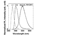
- 2 shows an emission spectrum of a TTP-PPT deposited film and an absorption spectrum of a C545T toluene solution.
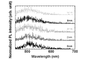
- 2 is a delayed fluorescence spectrum of each sample in which an mCP film is formed with a thickness of 0 to 8 nm. It is the graph which plotted PL quantum yield with respect to the thickness of a mCP film
- FIG. 3 is a graph showing the current density-external quantum efficiency characteristics of the organic electroluminescence device fabricated in Example 1.
- FIG. 4 is a graph showing current density-external quantum efficiency characteristics of an organic electroluminescence device fabricated in Example 2.
- FIG. 6 is a graph showing the current density-external quantum efficiency characteristics of the organic electroluminescence device fabricated in Example 3.
- 6 is a graph showing current density-external quantum efficiency characteristics of an organic electroluminescence element fabricated in Example 4.
- 6 is a graph showing current density-external quantum efficiency characteristics of an organic electroluminescence device manufactured in Comparative Example 1.
- a numerical range represented by using “to” means a range including numerical values described before and after “to” as a lower limit value and an upper limit value.
- the isotope species of the hydrogen atom present in the molecule of the compound used in the present invention is not particularly limited. For example, all the hydrogen atoms in the molecule may be 1 H, or a part or all of them are 2 H. (Deuterium D) may be used.
- the organic electroluminescent device of the present invention has an anode, a cathode, and an organic layer provided between the anode and the cathode.
- the organic layer includes at least two layers of a light emitting layer and a delayed fluorescence exciplex layer, and the present invention is characterized by having a delayed fluorescence exciplex layer. This feature will be described in detail later.
- An exemplary configuration of a typical organic electroluminescence element of the present invention is shown in FIG. In FIG.
- 1, 1 is a substrate, 2 is an anode, 3 is a hole injection layer, 4 is a hole transport layer, 5 is a light emitting layer, 6 is a triplet exciton blocking layer, 7 is a delayed fluorescence exciplex layer, 8 is An electron transport layer, 9 represents a cathode.
- the organic layer may be composed only of the light emitting layer and the delayed fluorescence exciplex layer as illustrated in FIG. 1A, or as illustrated in FIG. 1B or FIG. 1C. In addition to these, one having one or more organic layers may be used.
- Examples of such other organic layers include a triplet exciton blocking layer, a hole transport layer, a hole injection layer, an electron blocking layer, a hole blocking layer, an electron injection layer, an electron transport layer, and an exciton blocking layer.
- the hole transport layer may be a hole injection / transport layer having a hole injection function
- the electron transport layer may be an electron injection / transport layer having an electron injection function.
- the delayed fluorescence exciplex layer contains a donor compound and an acceptor compound, and holes and electrons injected from each of the anode and the cathode are recombined in the layer, thereby causing an excited state between the donor compound and the acceptor compound. And a reverse intersystem crossing from the excited triplet state to the excited singlet state occurs in this excited state.
- this excited state formed between the donor compound and the acceptor compound is referred to as “exciplex”.
- the excited state (exciplex) formed in the delayed fluorescence exciplex layer is excited single compared to the excited state formed by a single molecule due to the spatial separation of the two molecules forming the excited state. It is considered that the difference ⁇ Est between the term energy and the excited triplet energy is small. For this reason, in this delayed fluorescence exciplex layer, the reverse intersystem crossing from the excited triplet state to the excited singlet state occurs with a high probability.
- an organic electroluminescence device having such a delayed fluorescence exciplex layer
- holes are injected from the anode and electrons are injected from the cathode, and these holes and electrons are delayed.
- Recombination occurs in the plex layer, and an excited state is formed between the donor compound and the acceptor compound.
- the energy of the excited singlet state in the excited state moves to the light emitting material of the light emitting layer by the Forster mechanism, and excites the light emitting material to the singlet state.
- the excited triplet state crosses back to the excited singlet state with a certain probability determined by the compound species and other conditions, and excites the light emitting material of the light emitting layer to the singlet state by the same mechanism.
- the luminescent material excited to the singlet state emits fluorescence when returning to the ground state.
- the fluorescence emission resulting from the reverse intersystem crossing is observed as delayed fluorescence delayed from normal fluorescence (immediate fluorescence).
- the formation probability of the excited state formed by recombination of holes and electrons is larger in the excited triplet state than in the excited singlet state, but in this delayed fluorescence exciplex layer, the excited triplet state As a result, a high singlet exciton generation efficiency can be obtained. For this reason, the light emitting material of the light emitting layer can be efficiently fluorescently emitted by the mechanism as described above.
- the acceptor compound used in the exciplex layer is preferably a compound that satisfies the conditions of the formulas (3) and (4). That is, the excitation triplet energy (T 1 A ) defined by the short wavelength peak wavelength in the phosphorescence spectrum of the acceptor compound is the exciplex excitation singlet energy (S 1 ) defined by the peak wavelength of the exciplex emission. And the difference is preferably more than 0.2 eV. The difference between the excited triplet energy (T 1 A ) of the acceptor compound and the excited singlet energy (S 1 ) of the exciplex is more preferably greater than 0.3 eV, and even more preferably greater than 0.4 eV.
- ) of the acceptor compound is preferably more than 2.0 eV, more preferably more than 2.5 eV, and still more preferably more than 3.0 eV.
- acceptor compound examples include compounds represented by the following general formulas [1] to [4].
- Ar 1 , Ar 2 and Ar 3 in the general formula [1] each independently represent an aromatic hydrocarbon ring.
- Ar 1 , Ar 2 and Ar 3 may be the same or different, but are preferably the same.
- the aromatic hydrocarbon ring that Ar 1 , Ar 2, and Ar 3 can have preferably has 1 to 22 carbon atoms, more preferably 1 to 14 carbon atoms, and more preferably 1 to 10 carbon atoms. Further preferred.
- a benzene ring, a naphthalene ring, an anthracene ring, a phenanthrene ring, etc. can be mentioned, A benzene ring and a naphthalene ring are preferable and a benzene ring is more preferable.
- R 1 , R 2 and R 3 in the general formula [1] each independently represent a substituted or unsubstituted alkyl group or a substituted or unsubstituted alkoxy group.
- R 1 , R 2 and R 3 may be the same or different, but are preferably the same.
- R 1 , R 2 and R 3 are bonded to the ring as a substituent of the aromatic hydrocarbon ring of Ar 1 , Ar 2 and Ar 3 , respectively.
- the alkyl group that R 1 , R 2, and R 3 can take may be linear, branched, or cyclic. Preference is given to a linear or branched alkyl group.
- the alkyl group preferably has 1 to 20 carbon atoms, more preferably 1 to 12 carbon atoms, still more preferably 1 to 6 carbon atoms (ie, a methyl group, an ethyl group, n-propyl group, isopropyl group) is even more preferable.
- Examples of the cyclic alkyl group include a cyclopentyl group, a cyclohexyl group, and a cycloheptyl group.
- the alkyl group which R 1 , R 2 and R 3 can take may be substituted, and examples of the substituent in this case include an alkoxy group, an aryl group and an aryloxy group.
- the aryl group here may be composed of one aromatic ring, or may have a structure in which two or more aromatic rings are fused.
- the number of carbon atoms constituting the ring skeleton of the aryl group is preferably 6 to 22, more preferably 6 to 18, still more preferably 6 to 14, and more preferably 6 to 10 (that is, a phenyl group, Even more preferred are 1-naphthyl group, 2-naphthyl group).
- the aryloxy group herein may be composed of one aromatic ring or may have a structure in which two or more aromatic rings are fused.
- the number of carbon atoms constituting the ring skeleton of the aryloxy group is preferably 6 to 22, more preferably 6 to 18, still more preferably 6 to 14, and more preferably 6 to 10 (that is, phenyloxy Group, 1-naphthyloxy group, 2-naphthyloxy group) is even more preferable.
- the alkoxy group which R 1 , R 2 and R 3 can take may be linear, branched or cyclic. Preferred is a linear or branched alkoxy group.
- the alkoxy group preferably has 1 to 20 carbon atoms, more preferably 1 to 12 carbon atoms, still more preferably 1 to 6 carbon atoms (ie, a methoxy group, an ethoxy group, n-propoxy group, isopropoxy group) is even more preferable.
- Examples of the cyclic alkoxy group include a cyclopentyloxy group, a cyclohexyloxy group, and a cycloheptyloxy group.
- the alkoxy group which R 1 , R 2 and R 3 can take may be substituted, and examples of the substituent in this case include an alkoxy group, an aryl group and an aryloxy group.
- the above description can be referred to for the explanation and preferred range of the alkoxy group, aryl group, and aryloxy group herein.
- M1, m2 and m3 in the general formula [1] each independently represents an integer of 0 to 4. Preferably, it is an integer from 0 to 3.
- Ar 1 , Ar 2, and Ar 3 are benzene rings, a 3-substitution at the 2,4,6-position, a 2-substitution at the 3,5-position, a 1-substitution at the 2-position, a 1-substitution at the 3-position, Mention may be made of monosubstituted compounds at the 4-position.
- m1, m2 and m3 may be the same or different, but are preferably the same.
- a plurality of R 1 present in the molecule may be the same as or different from each other. The same applies to m2 and m3.
- Py 1 , Py 2 and Py 3 in the general formula [1] each independently represent a substituted or unsubstituted pyridyl group.
- Py 1 , Py 2 and Py 3 may be the same or different but are preferably the same.
- Py 1 , Py 2 and Py 3 are bonded to the ring as a substituent of the aromatic hydrocarbon ring of Ar 1 , Ar 2 and Ar 3 , respectively.
- Examples of the pyridyl group that can be taken by Py 1 , Py 2, and Py 3 include a 2-pyridyl group, a 3-pyridyl group, and a 4-pyridyl group, and any of them is preferable.
- the pyridyl group may be further substituted or unsubstituted.
- the substituent in the case where the pyridyl group is substituted include an alkyl group and an alkoxy group, and the description and preferred range thereof can be referred to the corresponding descriptions of R 1 , R 2 and R 3.
- n1, n2 and n3 each independently represents an integer of 1 to 3. Preferably, it is 1 or 2, for example, when Ar 1 , Ar 2, and Ar 3 are benzene rings, a 1-substituted product at the 3-position and a 2-substituted product at the 3,5-position can be mentioned.
- n1, n2 and n3 may be the same or different, but are preferably the same.
- n1 is 2 or more, a plurality of Py 1 present in the molecule may be the same as or different from each other. The same applies to n2 and n3.
- Y in the general formula [2] is S (sulfur atom) or SO 2 (sulfonyl group) is represented. * Represents a bonding position. That is, the general formula [2] includes the following three structures of the general formula [2-1], the general formula [2-2], and the general formula [2-3]. A structure represented by the general formula [2-2] is preferable.
- R 11 , R 12 , R 13 and R 14 are each independently Represents.
- Ar 11 and Ar 12 each independently represents a substituted or unsubstituted aryl group.
- Ar 11 and Ar 12 may be the same or different, but it is preferable that they are the same.
- a preferred example of Ar 11 and Ar 12 is a phenyl group.
- R 11 , R 12 , R 13 and R 14 may be the same or different, but are preferably the same.
- n11, n12, n13 and n14 each independently represents an integer of 0 to 2. Preferred is 0 or 1. However, the sum of n11, n12, n13 and n14 is 1 or more, preferably 1 to 4, more preferably 1 or 2. When the sum is 2 or more, multiple May be the same as or different from each other. Preferred is the same case.
- Z 21 in the general formula [3] is one of the following structures: Represents. X 1 and X 2 are both —CH ⁇ , X 1 is a single bond and X 2 is —CH ⁇ CH—, or X 1 is —CH ⁇ CH— and X 2 is a single bond.
- the ring skeleton containing X 1 and X 2 constitutes a benzene ring.
- p represents an integer of 0 to 3, and may be 0 or 1, for example.
- q represents an integer of 0 to 3, and may be 0 or 1, for example.
- L 21 in the general formula [3] represents a substituted or unsubstituted arylene group.
- the arylene group herein may be composed of one aromatic ring or may have a structure in which two or more aromatic rings are fused.
- the number of carbon atoms constituting the ring skeleton of the arylene group is preferably 6 to 22, more preferably 6 to 18, still more preferably 6 to 14, still more preferably 6 to 10,
- a 1,3-phenylene group, a 1,4-phenylene group, a 1,5-naphthylene group and a 2,6-naphthylene group are even more preferable, and a 1,3-phenylene group and a 1,4-phenylene group are particularly preferable.
- Examples of the substituent when the arylene group is substituted include an alkyl group, an alkoxy group, an aryl group, and an aryloxy group.
- the explanation and preferred range thereof correspond to those in the general formula [1]. Reference can be made to the description.
- Py 21 in the general formula [3] represents a substituted or unsubstituted pyridyl group.
- the corresponding description in the general formula [1] can be referred to.
- N21 in the general formula [3] represents an integer of 2 to 6.
- it is an integer of 2 to 4, more preferably 3 or 4.
- a plurality of (L 21 -Py 21 ) present in the molecule may be the same as or different from each other. Preferred is the same case.
- L 31 , L 32 and L 33 in the general formula [4] each independently represent a single bond or a substituted or unsubstituted arylene group.
- L 31 , L 32 and L 33 may be the same or different, but are preferably the same.
- the corresponding description in the general formula [3] can be referred to.
- a 1,3-phenylene group can be employed.
- Py 31 , Py 32 and Py 33 in the general formula [4] each independently represent a substituted or unsubstituted pyridyl group.
- Py 31 , Py 32 and Py 33 may be the same or different, but are preferably the same.
- N31, n32 and n33 in the general formula [4] each independently represents an integer of 1 to 3, and is preferably 1 or 2.
- a trisubstituted product at the 2,4,6 position, a disubstituted product at the 3,5 position, a 1 substituted product at the 3 position, and a 1 substituted product at the 4 position can be exemplified.
- n31, n32 and n33 may be the same or different, but are preferably the same.
- a plurality of (L 31 -Py 31 ) present in the molecule may be the same as or different from each other. Preferred is the same case. The same applies to n32 and n33.
- the acceptor compound used in the present invention is commercially available, or can be synthesized by combining known synthesis methods as necessary.
- the donor compound used for the exciplex layer is preferably a compound that satisfies the conditions of the formulas (5) and (6). That is, the excitation triplet energy (T 1 D ) defined by the short wavelength peak wavelength in the phosphorescence spectrum of the donor compound is the exciplex excitation singlet energy (S 1 ) defined by the peak wavelength of the exciplex emission. And the difference is preferably 0.2 eV or more. The difference between the excited triplet energy (T 1 D ) of the donor compound and the excited singlet energy (S 1 ) of the exciplex is more preferably greater than 0.3 eV, and even more preferably greater than 0.4 eV.
- ) of the donor compound is preferably 5.3 eV or less, more preferably less than 5.2 eV, and even more preferably less than 5.1 eV.
- Preferred examples of the donor compound include compounds represented by the following general formulas [11] to [15].
- R 51 , R 52 , R 53 , R 54 , R 55 and R 56 each independently represent a substituted or unsubstituted alkyl group or a substituted or unsubstituted alkoxy group.
- R 51 , R 52 , R 53 , R 54 , R 55 and R 56 may be the same or different, but are preferably the same.
- the corresponding description in the general formula [1] can be referred to.
- n51, n52, n53, n54, n55 and n56 each independently represents an integer of 0 to 5. Preferably, it is an integer from 0 to 3, more preferably from 0 to 2.
- n51, n52, n53, n54, n55 and n56 may be the same or different, but n51, n53 and n55 are preferably the same, and n52, n54 and n56 are preferably the same.
- n51, n53, and n55 are 1 or 2 and n52, n54, and n56 are 0 is preferable.
- substitution form examples include a 3-substituted product at the 2,4,6-position, a 2-substituted product at the 3,5-position, a 1-substituted product at the 2-position, a 1-substituted product at the 3-position, and a 1-substituted product at the 4-position.
- n51 is 2 or more
- the plurality of R 51 present in the molecule may be the same as or different from each other. Preferred is the same case.
- two R 51 among the plural R 51 present in the molecule is attached to a carbon atom adjacent the benzene ring, the two R 51 are to form a linking group bonded to each other Also good.
- the two R 51 are bonded to each other to form a linking group, thereby forming a ring fused to the benzene ring.
- the number of linking chain atoms of the linking group formed by bonding two R 51 to each other is preferably 3 to 5, and more preferably 3 or 4.
- Examples of the linking group include an alkylene group and an alkenylene group. Preferred examples include —CH ⁇ CH—CH ⁇ CH— and a linking group in which at least one of the four hydrogen atoms is substituted with a substituted or unsubstituted alkyl group or a substituted or unsubstituted alkoxy group. it can.
- n51 is the same for n52, n53, n54, n55 and n56.
- R 61 , R 62 , R 63 , R 64 , R 65 and R 66 in the general formula [12] each independently represent a substituted or unsubstituted alkyl group or a substituted or unsubstituted alkoxy group.
- R 61 , R 62 , R 63 , R 64 , R 65 and R 66 may be the same or different, but are preferably the same.
- M61, m62 and m63 in the general formula [12] each independently represents either 1 or 2.
- a 3-substituted 2-substituted product, a 3-position mono-substituted product, and a 4-position mono-substituted product can be exemplified.
- m61 is 2 or more, a plurality of molecules present in the molecule May be the same as or different from each other. Preferred is the same case.
- m62 and m63 may be the same or different, but are preferably the same.
- n61, n62, n63, n64, n65 and n66 each independently represents an integer of 0 to 5. An integer from 0 to 3 is preferable, and an integer from 0 to 2 is more preferable.
- n61 is 2 or more
- the plurality of R 61 present in the molecule may be the same as or different from each other. Preferred is the same case.
- two R 61 among the plural R 61 present in the molecule is attached to a carbon atom adjacent the benzene ring, the two R 61 are to form a linking group bonded to each other Also good.
- the two R 61 are bonded to each other to form a linking group, a ring fused to the benzene ring is formed.
- the number of linking chain atoms of the linking group formed by bonding two R 61 to each other is preferably 3 to 5, and more preferably 3 or 4.
- the linking group include an alkylene group and an alkenylene group.
- Preferred examples include —CH ⁇ CH—CH ⁇ CH— and a linking group in which at least one of the four hydrogen atoms is substituted with a substituted or unsubstituted alkyl group or a substituted or unsubstituted alkoxy group. it can.
- the substituted or unsubstituted alkyl group and the substituted or unsubstituted alkoxy group here, the corresponding description in the general formula [1] can be referred to.
- n61 is the same for n62, n63, n64, n65 and n66.
- n61, n62, n63, n64, n65 and n66 may be the same or different, but are preferably the same.
- R 71 , R 72 , R 73 and R 74 in the general formula [13] are each independently a substituted or unsubstituted alkyl group, a substituted or unsubstituted alkoxy group, or Represents.
- R 75 and R 76 each independently represents a substituted or unsubstituted alkyl group or a substituted or unsubstituted alkoxy group.
- R 71 , R 72 , R 73 and R 74 may be the same or different, but are preferably the same.
- M71 in the general formula [13] represents 0 or 1, and both are preferable.
- n71, n72, n73, n74, n75 and n76 each independently represents an integer of 0 to 5.
- it is an integer from 0 to 3, more preferably from 0 to 2.
- a 3-substitution at the 2,4,6-position, a 2-substitution at the 3,5-position, a 1-substitution at the 2-position, a 1-substitution at the 3-position, and a 1-substitution at the 4-position can be mentioned.
- the plurality of R 71 present in the molecule may be the same as or different from each other. Preferred is the same case.
- the two R 71 among the plural R 71 present in the molecule is attached to a carbon atom adjacent the benzene ring, the two R 71 are to form a linking group bonded to each other Also good.
- the two R 71 's are bonded to each other to form a linking group, thereby forming a ring fused to the benzene ring.
- the number of linking chain atoms of the linking group formed by bonding two R 71 to each other is preferably 3 to 5, and more preferably 3 or 4.
- Examples of the linking group include an alkylene group and an alkenylene group.
- Preferred examples include —CH ⁇ CH—CH ⁇ CH— and a linking group in which at least one of the four hydrogen atoms is substituted with a substituted or unsubstituted alkyl group or a substituted or unsubstituted alkoxy group. it can.
- the substituted or unsubstituted alkyl group and the substituted or unsubstituted alkoxy group here, the corresponding description in the general formula [1] can be referred to.
- the above description regarding n71 is the same for n72, n73, n74, n75 and n76.
- n71, n72, n73 and n74 may be the same or different, but are preferably the same.
- N75 and n76 may be the same or different, but are preferably the same.
- Q in the general formula [14] represents an atomic group necessary for forming a cyclic structure.
- Q is preferably a substituted or unsubstituted alkylene group, a substituted or unsubstituted alkenylene group, a substituted or unsubstituted alkynylene group, and is a substituted or unsubstituted alkylene group or a substituted or unsubstituted alkenylene group. Is more preferable, and a substituted or unsubstituted alkylene group is more preferable.
- the number of carbon atoms constituting the ring skeleton of Q is preferably 4 to 10, more preferably 5 to 8, and still more preferably 5 to 7.
- Q examples include a butylene group, a pentylene group, a hexylene group, and a butadienylene group.
- substituent of the alkylene group, alkenylene group, and alkynylene group that Q can take include an alkyl group, an alkoxy group, an aryl group, and an aryloxy group.
- R 1 , R 2 and R 3 can be referred to.
- the alkylene group, alkenylene group and alkynylene group which Q can take are also preferably unsubstituted.
- R 81 , R 82 , R 83 and R 84 in the general formula [14] each independently represent a substituted or unsubstituted alkyl group or a substituted or unsubstituted alkoxy group.
- R 81 , R 82 , R 83 and R 84 see the corresponding description in the general formula [1]. Can do.
- n81, n82, n83 and n84 each independently represents an integer of 0 to 5. Preferably, it is an integer from 0 to 3, more preferably from 0 to 2.
- a 3-substitution at the 2,4,6-position, a 2-substitution at the 3,5-position, a 1-substitution at the 2-position, a 1-substitution at the 3-position, and a 1-substitution at the 4-position can be mentioned.
- n81 is 2 or more, the plurality of R 81 present in the molecule may be the same as or different from each other. Preferred is the same case.
- the two R 81 among the plural R 81 present in the molecule is attached to a carbon atom adjacent the benzene ring, the two R 81 are to form a linking group bonded to each other Also good.
- the two R 81 are bonded to each other to form a linking group, whereby a ring fused to the benzene ring is formed.
- the number of linking chain atoms of the linking group formed by bonding two R 71 to each other is preferably 3 to 5, and more preferably 3 or 4.
- Examples of the linking group include an alkylene group and an alkenylene group.
- Preferred examples include —CH ⁇ CH—CH ⁇ CH— and a linking group in which at least one of the four hydrogen atoms is substituted with a substituted or unsubstituted alkyl group or a substituted or unsubstituted alkoxy group. it can.
- the substituted or unsubstituted alkyl group and the substituted or unsubstituted alkoxy group here, the corresponding description in the general formula [1] can be referred to.
- the above description regarding n81 is the same for n82, n83 and n84.
- n81, n82, n83 and n84 may be the same or different but are preferably the same.
- R 91 and R 92 in the general formula [15] each independently represent a substituted or unsubstituted alkyl group or a substituted or unsubstituted aryl group.
- R 91 and R 92 in the general formula [15] each independently represent a substituted or unsubstituted alkyl group or a substituted or unsubstituted aryl group.
- the donor compound used in the present invention is commercially available, or can be synthesized by combining known synthesis methods as necessary.
- the acceptor compound and the donor compound are mixed to form a mixture.
- the molar content of the donor compound in the mixture is preferably more than 0.2 and less than 0.6, more preferably more than 0.3 and less than 0.6. Preferably, it is more preferably more than 0.4 and less than 0.6.
- the combination of the acceptor compound and the donor compound is not particularly limited as long as it can form an exciplex. The following table illustrates preferred combinations of acceptor compounds and donor compounds.
- Examples of particularly preferred combinations include the following 1, 3, 8, 11, 18, 37, 38, more preferably 37 (donor compound: TTP, acceptor compound: PPT), 38 (donor compound: dPTBdA, Acceptor compound: PPT). Furthermore, a combination of a donor compound: CzTTP1 and an acceptor compound: PPT can also be suitably used.
- the delayed fluorescence exciplex layer 31 has a singlet exciton generation efficiency as high as 65 to 100%, and can efficiently cause the light emitting material of the light emitting layer to emit fluorescence.
- the delayed exciplex layer of 32 and the combination of CzTTP1 and PPT is unlikely to cause dexter transfer of excited triplet energy, a triplet exciton blocking layer to be described later is not necessary, and the configuration of the organic electroluminescence device can be reduced. There is an effect that it can be done simply.
- the method for forming the delayed fluorescence exciplex layer is not particularly limited, and examples thereof include a co-evaporation method.
- the thickness of the delayed fluorescence exciplex layer is not particularly limited, but is preferably 10 to 120 nm, more preferably 10 to 60 nm, and even more preferably 10 to 30 nm. By selecting the thickness of the delayed fluorescence exciplex layer from the above range, a delayed fluorescence exciplex layer with high singlet exciton generation efficiency can be obtained.
- the light emitting layer is a layer that contains a light emitting material and emits light when the light emitting material is excited by energy transfer from the delayed fluorescence exciplex layer and then returns to the ground state.
- recombination of holes and electrons may occur in the light emitting layer.
- a part of the light-emitting material contained in the light-emitting layer may be excited by such recombination of holes and electrons, and then emit light when returning to the ground state.
- the positional relationship between the light emitting layer and the delayed fluorescence exciplex layer may be such that the delayed fluorescence exciplex layer is closer to the cathode than the light emitting layer, or may be closer to the anode.
- the light emitting material used for the light emitting layer is preferably a fluorescent material.
- a fluorescent material thereby, singlet excitons efficiently generated in the delayed fluorescence exciplex layer can be effectively contributed to the light emission of the light emitting material, and an organic electroluminescence device with high light emission efficiency can be realized.
- a delayed fluorescent material may be used as the fluorescent material.
- the delayed fluorescent material is excited to an excited singlet state and an excited triplet state by carrier recombination, but when excited to an excited triplet state, at least a part of the delayed fluorescent material is brought to an excited singlet state by reverse intersystem crossing.
- a transitional fluorescent material is used as the light emission of the light emitting layer includes both fluorescence (immediate fluorescence) and delayed fluorescence.
- C545T has a PL quantum yield of 91.3% in a toluene solution, and can obtain very high luminous efficiency.
- the range of the luminescent material which can be used by this invention is not limitedly interpreted by the following specific examples.
- the light emitting layer may be composed of a light emitting material alone, but preferably contains a host compound having the light emitting material as a guest compound.
- a host compound an organic compound satisfying the following formula (1) can be used between a donor compound and an acceptor compound included in the delayed fluorescence exciplex layer and a guest compound that is a light-emitting material.
- Formula (1) ES 1 > ES 1 G and ES 1 H > ES 1 G [In Formula (1), ES 1 represents the lowest excited singlet energy level of the exciplex formed by the donor compound and the acceptor compound, ES 1 H represents the lowest excited singlet energy level of the host compound, ES 1 G represents the lowest excited singlet energy level of the guest compound.
- the “minimum excited singlet energy level” in the present invention can be measured by the following method.
- the following method demonstrates the case where a measuring object compound and mCBP are used.
- a sample having a thickness of 100 nm is prepared on a Si substrate by co-evaporating the measurement target compound and mCBP so that the measurement target compound has a concentration of 6% by weight.
- the fluorescence spectrum of this sample is measured at room temperature (300K). By integrating the luminescence from immediately after the excitation light incidence to 100 nanoseconds after the incidence, a fluorescence spectrum having the vertical axis indicating phosphorescence intensity and the horizontal axis indicating wavelength is obtained.
- the fluorescence spectrum has light emission on the vertical axis and wavelength on the horizontal axis.
- the lowest excited singlet energy level ES 1 G of the guest compound is less than the lowest excited singlet energy level ES 1 of the exciplex formed by the donor compound and the acceptor compound.
- the excitation singlet energy of this exciplex can be efficiently transferred to the guest compound.
- the lowest excited singlet energy level ES 1 G of the guest compound is lower than the lowest excited singlet energy level ES 1 H of the host compound, the excited singlet energy of the host compound is efficiently transferred to the guest compound.
- the excited singlet energy of the guest compound can be reliably confined in the guest compound.
- the excited singlet energy generated in the delayed fluorescence exciplex layer or the like can be efficiently converted into the light emission of the light emitting material, and an organic electroluminescence device with high light emission efficiency can be realized.
- Either the lowest excited singlet energy level ES 1 of the exciplex formed by the donor compound and the acceptor compound and the lowest excited singlet energy level ES 1 H of the host compound may be low, but ES 1 > If it is ES 1 H , the excited singlet energy of the exciplex can be efficiently transferred by the host compound. Note that part of the light emitted from the light emitting layer may be emitted from the host material.
- the lowest excited singlet energy level ES 1 of the exciplex formed by the donor compound and the acceptor compound is preferably 1.9 to 3.1 eV, more preferably 2.1 to 2.9 eV. More preferably, it is 2.3 to 2.7 eV.
- the lowest excited singlet energy level ES 1 H of the host compound is preferably 1.9 to 3.3 eV, more preferably 2.1 to 3.1 eV, and 2.3 to 2. More preferably, it is 8 eV.
- the lowest excited singlet energy level ES 1 G of the guest compound is preferably 1.9 to 3.1 eV, more preferably 2.0 to 2.9 eV, and 2.1 to 2. More preferably, it is 7 eV.
- the amount of the light emitting material contained in the light emitting layer is preferably 0.1% by weight or more, more preferably 1% by weight or more, and 50% by weight or less. Is preferably 20% by weight or less, more preferably 10% by weight or less.
- the host material in the light-emitting layer is an organic compound that satisfies the condition of the formula (1), has a hole transporting ability and an electron transporting ability, prevents the emission of longer wavelengths, and has a high glass transition temperature. It is preferable. Specific examples of preferable compounds that can be used as a host material in the present invention are given below. The range of the host material that can be used in the present invention is not limitedly interpreted by the following specific examples.
- Triplet exciton blocking layer When the organic electroluminescence device of the present invention employs a system in which dexter transfer of excited triplet energy frequently occurs from the delayed fluorescence exciplex layer to the light emitting layer, for example, as in Example 4, the light emitting layer and the delay A triplet exciton blocking layer is preferably provided between the fluorescent exciplex layer.
- the triplet exciton blocking layer has a function of suppressing transfer of excited triplet energy from the delayed fluorescence exciplex layer to the light emitting layer. By providing this triplet exciton blocking layer, the light emission efficiency of the organic electroluminescence device can be further increased for the following reasons.
- the delayed fluorescence exciplex layer in the delayed fluorescence exciplex layer, an inverse intersystem crossing from the excited triplet state to the excited singlet state occurs, but the excited triplet state is adjacent before the reverse intersystem crossing occurs. May transfer energy to the organic layer.
- the light emitting material of the light emitting layer receives the excited triplet energy from the delayed fluorescence exciplex layer, the light emitting material is deactivated without emitting light, and the energy is wasted.
- a triplet exciton blocking layer is provided between the light emitting layer and the delayed fluorescence exciplex layer, the transfer of excited triplet energy from the delayed fluorescence exciplex layer to the light emitting layer is suppressed, and the delayed fluorescence excitation is suppressed.
- the excited triplet state formed in the plex layer can be reliably crossed between inverse terms to contribute to fluorescence emission. As a result, the luminous efficiency of the organic electroluminescence element can be further increased.
- the formation of such a triplet exciton blocking layer is unnecessary, and organic electroluminescence
- Examples of such delayed fluorescence exciplex layer include a combination of CzTTP1 and PPT, a combination of dBTBdA and PPT, and the like.
- a condition of the following formula (2) is satisfied between a donor compound and an acceptor compound contained in the delayed fluorescence exciplex layer and a host compound and a guest compound contained in the light emitting layer. It is preferable to use a filling organic compound (blocking compound).
- Formula (2) ET 1 B > ET 1 > ET 1 H > ET 1 G [In Formula (2), ET 1 B represents the lowest excited triplet energy level of the blocking compound, ET 1 represents the lowest excited triplet energy level of the exciplex formed by the donor compound and the acceptor compound, ET 1 H represents the lowest excited triplet energy level of the host compound, and ET 1 G represents the lowest excited triplet energy level of the guest compound.
- the “lowest excited triplet energy level” in the present invention can be measured by the following method.
- the following method demonstrates the case where a measuring object compound and mCBP are used.
- the same sample used for the measurement of the singlet energy E S1 is cooled to 5 [K]
- the sample for phosphorescence measurement is irradiated with excitation light (337 nm), and the phosphorescence intensity is measured using a streak camera. .
- a phosphorescence spectrum with the vertical axis representing phosphorescence intensity and the horizontal axis representing wavelength is obtained.
- the value converted to the energy value conversion equation shown below peak wavelength value ⁇ of the short side of the emission spectrum and E S1. Conversion formula: E T1 [eV] 1239.85 / ⁇ edge
- Exciplex lowest excited triplet energy level ET 1 host compound lowest excited triplet energy level ET 1 H , guest compound lowest excited triplet energy level ET with no triplet exciton blocking layer
- 1 G has a relationship of ET 1 > ET 1 H > ET 1 G
- the excited triplet state formed in the delayed fluorescence exciplex layer easily transfers energy to the guest compound via the host compound.
- an organic compound layer having a lowest excited triplet energy level ET 1 B larger than the lowest excited triplet energy level ET 1 of the exciplex is delayed with the light emitting layer.
- this organic compound layer functions as a triplet exciton blocking layer, and the transfer of excited triplet energy from the delayed fluorescent exciplex layer to the light emitting layer can be suppressed.
- the lowest excited triplet energy level ET 1 B of the blocking compound is preferably 2.0 to 3.2 eV, more preferably 2.2 to 3.0 eV, and 2.4 to 2.9 eV. More preferably it is.
- the lowest excited triplet energy level ET 1 of the exciplex formed by the donor compound and the acceptor compound is preferably 1.9 to 3.1 eV, more preferably 2.1 to 2.9 eV. More preferably, it is 2.3 to 2.8 eV.
- the lowest excited triplet energy level ET 1 H of the host compound is preferably 1.9 to 3.1 eV, more preferably 2.1 to 2.9 eV, and 2.3 to 2. More preferably, it is 8 eV.
- mCP has a high lowest excited triplet energy level ET 1 B , it can be suitably used as a constituent material of the triplet exciton blocking layer.
- the thickness of the triplet exciton blocking layer is preferably selected in consideration of R 0 as the Forster moving radius between the exciplex of the delayed fluorescence exciplex layer and the light emitting material of the light emitting layer. Specifically, it is desirable that the film thickness of the triplet exciton blocking layer is sufficiently larger than 2 nm, which is a general Dexter energy transfer distance, and smaller than the Forster moving radius.
- the Forster moving radius is measured by the molar absorption coefficient of the guest compound and the emission spectrum of the delayed fluorescence exciplex.
- the thickness of the triplet exciton blocking layer is determined by the energy by the Forster mechanism.
- the excited singlet energy generated in the delayed fluorescence exciplex layer can be efficiently transferred to the light emitting layer.
- the Forster moving radius R 0 is 3.5 nm.
- the thickness of the triplet exciton blocking layer is preferably 2 to 8 nm, more preferably 3 to 5 nm, and 3.5 to 4.5 nm. Most preferably it is.
- the organic electroluminescence device of the present invention may have the following organic layers in addition to the delayed fluorescence exciplex layer, the light emitting layer, and the triplet exciton blocking layer.
- the injection layer is a layer provided between the electrode and the organic layer for lowering the driving voltage and improving the luminance of light emission, and includes a hole injection layer and an electron injection layer, Further, it may be present between the cathode and the light emitting layer or the electron transport layer.
- the injection layer can be provided as necessary.
- the blocking layer is a layer that can prevent diffusion of charges (electrons or holes) and / or excitons existing in the light emitting layer to the outside of the light emitting layer.
- the electron blocking layer can be disposed between the light emitting layer and the hole transport layer and blocks electrons from passing through the light emitting layer toward the hole transport layer.
- a hole blocking layer can be disposed between the light emitting layer and the electron transporting layer to prevent holes from passing through the light emitting layer toward the electron transporting layer.
- the blocking layer can also be used to block excitons from diffusing outside the light emitting layer. That is, each of the electron blocking layer and the hole blocking layer can also function as an exciton blocking layer.
- the term “electron blocking layer” or “exciton blocking layer” as used herein is used in the sense of including a layer having the functions of an electron blocking layer and an exciton blocking layer in one layer.
- the hole blocking layer has a function of an electron transport layer in a broad sense.
- the hole blocking layer has a role of blocking holes from reaching the electron transport layer while transporting electrons, thereby improving the recombination probability of electrons and holes in the light emitting layer.
- the material for the hole blocking layer the material for the electron transport layer described later can be used as necessary.
- the electron blocking layer has a function of transporting holes in a broad sense.
- the electron blocking layer has a role to block electrons from reaching the hole transport layer while transporting holes, thereby improving the probability of recombination of electrons and holes in the light emitting layer. .
- the exciton blocking layer is a layer for preventing excitons generated by recombination of holes and electrons in the light emitting layer from diffusing into the charge transport layer. It becomes possible to efficiently confine in the light emitting layer, and the light emission efficiency of the device can be improved.
- the exciton blocking layer can be inserted on either the anode side or the cathode side adjacent to the light emitting layer, or both can be inserted simultaneously.
- the layer when the exciton blocking layer is provided on the anode side, the layer can be inserted adjacent to the light emitting layer between the hole transport layer and the light emitting layer, and when inserted on the cathode side, the light emitting layer and the cathode Between the luminescent layer and the light-emitting layer.
- a hole injection layer, an electron blocking layer, or the like can be provided between the anode and the exciton blocking layer adjacent to the anode side of the light emitting layer, and the excitation adjacent to the cathode and the cathode side of the light emitting layer can be provided.
- an electron injection layer, an electron transport layer, a hole blocking layer, and the like can be provided.
- the blocking layer is disposed, at least one of the excited singlet energy and the excited triplet energy of the material used as the blocking layer is preferably higher than the excited singlet energy and the excited triplet energy of the light emitting material.
- the hole transport layer is made of a hole transport material having a function of transporting holes, and the hole transport layer can be provided as a single layer or a plurality of layers.
- the hole transport material has any one of hole injection or transport and electron barrier properties, and may be either organic or inorganic.
- hole transport materials that can be used include, for example, triazole derivatives, oxadiazole derivatives, imidazole derivatives, carbazole derivatives, indolocarbazole derivatives, polyarylalkane derivatives, pyrazoline derivatives and pyrazolone derivatives, phenylenediamine derivatives, arylamine derivatives, Examples include amino-substituted chalcone derivatives, oxazole derivatives, styrylanthracene derivatives, fluorenone derivatives, hydrazone derivatives, stilbene derivatives, silazane derivatives, aniline copolymers, and conductive polymer oligomers, particularly thiophene oligomers.
- An aromatic tertiary amine compound and an styrylamine compound are preferably used, and an aromatic tertiary amine compound is more preferably used.
- the electron transport layer is made of a material having a function of transporting electrons, and the electron transport layer can be provided as a single layer or a plurality of layers.
- the electron transport material (which may also serve as a hole blocking material) may have a function of transmitting electrons injected from the cathode to the light emitting layer.
- Examples of the electron transport layer that can be used include nitro-substituted fluorene derivatives, diphenylquinone derivatives, thiopyrandioxide derivatives, carbodiimides, fluorenylidenemethane derivatives, anthraquinodimethane and anthrone derivatives, oxadiazole derivatives, and the like.
- a thiadiazole derivative in which the oxygen atom of the oxadiazole ring is substituted with a sulfur atom, and a quinoxaline derivative having a quinoxaline ring known as an electron withdrawing group can also be used as an electron transport material.
- a polymer material in which these materials are introduced into a polymer chain or these materials are used as a polymer main chain can also be used.
- the preferable material which can be used for an organic electroluminescent element is illustrated concretely.
- the material that can be used in the present invention is not limited to the following exemplary compounds.
- R, R ′, and R 1 to R 10 each independently represent a hydrogen atom or a substituent.
- X represents a carbon atom or a hetero atom forming a ring skeleton
- n represents an integer of 3 to 5
- Y represents a substituent
- m represents an integer of 0 or more.
- the method for forming the organic layer described above is not particularly limited, and may be produced by either a dry process or a wet process.
- the organic electroluminescence device of the present invention is preferably supported on a substrate.
- the substrate is not particularly limited and may be any substrate conventionally used for organic electroluminescence elements.
- a substrate made of glass, transparent plastic, quartz, silicon, or the like can be used.
- an electrode material made of a metal, an alloy, an electrically conductive compound, or a mixture thereof having a high work function (4 eV or more) is preferably used.
- electrode materials include metals such as Au, and conductive transparent materials such as CuI, indium tin oxide (ITO), SnO 2 , and ZnO.
- conductive transparent materials such as CuI, indium tin oxide (ITO), SnO 2 , and ZnO.
- an amorphous material such as IDIXO (In 2 O 3 —ZnO) that can form a transparent conductive film may be used.
- a thin film may be formed by vapor deposition or sputtering of these electrode materials, and a pattern of a desired shape may be formed by photolithography, or when pattern accuracy is not so high (about 100 ⁇ m or more) ), A pattern may be formed through a mask having a desired shape at the time of vapor deposition or sputtering of the electrode material.
- wet film-forming methods such as a printing system and a coating system, can also be used.
- the transmittance be greater than 10%, and the sheet resistance as the anode is preferably several hundred ⁇ / ⁇ or less.
- the film thickness depends on the material, it is usually selected in the range of 10 to 1000 nm, preferably 10 to 200 nm.
- cathode a material having a low work function (4 eV or less) metal (referred to as an electron injecting metal), an alloy, an electrically conductive compound, and a mixture thereof as an electrode material is used.
- electrode materials include sodium, sodium-potassium alloy, magnesium, lithium, magnesium / copper mixture, magnesium / silver mixture, magnesium / aluminum mixture, magnesium / indium mixture, aluminum / aluminum oxide (Al 2 O 3 ) Mixtures, indium, lithium / aluminum mixtures, rare earth metals and the like.
- a mixture of an electron injecting metal and a second metal which is a stable metal having a larger work function value than this for example, a magnesium / silver mixture
- Suitable are a magnesium / aluminum mixture, a magnesium / indium mixture, an aluminum / aluminum oxide (Al 2 O 3 ) mixture, a lithium / aluminum mixture, aluminum and the like.
- the cathode can be produced by forming a thin film of these electrode materials by a method such as vapor deposition or sputtering.
- the sheet resistance as the cathode is preferably several hundred ⁇ / ⁇ or less, and the film thickness is usually selected in the range of 10 nm to 5 ⁇ m, preferably 50 to 200 nm.
- the emission luminance is advantageously improved.
- a transparent or semi-transparent cathode can be produced. By applying this, an element in which both the anode and the cathode are transparent is used. Can be produced.
- the organic electroluminescence device of the present invention has the above-described configuration, and emits light when an electric field is applied between the anode and the cathode. At this time, the organic electroluminescence device of the present invention has a delayed fluorescence exciplex layer, whereby an excited singlet state is efficiently formed in the delayed fluorescence exciplex layer, and the energy of the excited singlet state is The light emitting material can be efficiently fluorescently emitted by moving to the light emitting material. For this reason, this organic electroluminescent element can obtain high luminous efficiency.
- the organic electroluminescence element of the present invention can be applied to any of a single element, an element having a structure arranged in an array, and a structure in which an anode and a cathode are arranged in an XY matrix. According to the present invention, an organic light emitting device with greatly improved light emission efficiency can be obtained by containing the compound represented by the general formula (1) in the light emitting layer.
- the organic light emitting device such as the organic electroluminescence device of the present invention can be further applied to various uses. For example, it is possible to produce an organic electroluminescence display device using the organic electroluminescence element of the present invention.
- organic electroluminescence device of the present invention can be applied to organic electroluminescence illumination and backlights that are in great demand.
- each organic layer was formed using a vacuum deposition method at a degree of vacuum of 1.0 ⁇ 10 ⁇ 4 to 1.0 ⁇ 10 ⁇ 3 Pa.
- the values of the lowest excited singlet energy level and the lowest excited triplet energy level of each material used in Examples and Comparative Examples are summarized in Table 2 below.
- Example 1 A glass substrate on which an anode made of indium tin oxide (ITO) having a thickness of 100 nm was formed was prepared. On the anode of the glass substrate, CzTTP1 was formed to a thickness of 35 nm to obtain a hole transport layer. Next, CzTTP1 and PPT were co-evaporated from different vapor deposition sources to form a layer having a thickness of 30 nm to form a delayed fluorescence exciplex layer. At this time, the concentration of CzTTP1 was 30 mol%. Next, C545T and PPT were co-evaporated from different vapor deposition sources to form a 10 nm thick layer as a light emitting layer.
- ITO indium tin oxide
- the concentration of C545T was 1% by weight.
- PPT was formed to a thickness of 25 nm to obtain an electron transport layer.
- lithium fluoride (LiF) was vapor-deposited to a thickness of 0.8 nm, and then aluminum (Al) was vapor-deposited to a thickness of 80 nm to form a cathode, whereby an organic electroluminescence element was obtained.
- Example 2 An organic electroluminescence device was produced in the same manner as in Example 1 except that dPTBdA was used instead of CzTTP1 as the material for the hole transport layer and the donor compound for the delayed fluorescence exciplex layer.
- Example 3 An organic electroluminescence device was produced in the same manner as in Example 2 except that the concentration of dPTBdA in the delayed exciplex layer was 50 mol%.
- Example 4 (Examination of film thickness of triplet exciton blocking layer)
- a triplet exciton blocking layer (mCP vapor deposition film) is formed between the light emitting layer (C545T-CBP vapor deposition film) and the delayed fluorescence exciplex layer (TTP-PPT vapor deposition film).
- the film thickness of the triplet exciton blocking layer was examined.
- FIG. 2 shows an emission spectrum of a TTP-PPT deposited film in which TTP and PPT are co-deposited at 50 mol% and an absorption spectrum of a C545T toluene solution. From FIG.
- the peak observed in the range of 450 to 490 nm is a peak derived from delayed fluorescence from the delayed fluorescence exciplex layer, and this peak is observed due to the excitation triplet from the delayed fluorescence exciplex layer to the light emitting layer. It means that Dexter movement of term energy is suppressed. From this point of view, a peak derived from delayed fluorescence is observed on the short wavelength side in the sample in which mCP is formed with a thickness of 2 to 8 nm, whereas in the sample in which mCP is not formed, this delay is observed. The peak derived from fluorescence disappears.
- the mCP film has a function of suppressing the dexter transfer of excited triplet energy from the delayed fluorescence exciplex layer to the light emitting layer.
- the PL quantum yield is highest in the sample with the 4 nm mCP film, and the sample with the mCP film formed at 2 nm, 6 nm, and 8 nm is higher than the sample without the mCP film formed.
- the thickness of the mCP film is preferably 2 to 8 nm, and optimally 4 nm.
- organic electroluminescence device having a 4 nm thick mCP film as a triplet exciton blocking layer was produced as follows.
- ⁇ -NPD was formed to a thickness of 40 nm to obtain a hole transport layer.
- C545T and CBP were co-evaporated from different vapor deposition sources to form a 10 nm thick layer as a light emitting layer. At this time, the concentration of C545T was 2.5% by weight.
- mCP was formed to a thickness of 4 nm to obtain a triplet exciton blocking layer.
- TTP and PPT were co-deposited from different vapor deposition sources to form a 30 nm thick layer to form a delayed fluorescence exciplex layer. At this time, the concentration of TTP was 50 mol%.
- PPT was formed to a thickness of 40 nm to obtain an electron transport layer.
- lithium fluoride (LiF) was vapor-deposited to a thickness of 0.75 nm, and then aluminum (Al) was vapor-deposited to a thickness of 70 nm to form a cathode, whereby an organic electroluminescence element was obtained.
- a glass substrate on which an anode made of indium tin oxide (ITO) having a thickness of 100 nm was formed was prepared.
- TTP was formed to a thickness of 20 nm to obtain a hole transport layer.
- TTP and PPT were co-evaporated from different vapor deposition sources to form a layer having a thickness of 60 nm as a light emitting layer. At this time, the concentration of TTP was 50 mol%.
- PPT was formed to a thickness of 20 nm to obtain an electron transport layer.
- lithium fluoride (LiF) was vapor-deposited to a thickness of 0.75 nm, and then aluminum (Al) was vapor-deposited to a thickness of 70 nm to form a cathode, whereby an organic electroluminescence element was obtained.
- FIG. 5 shows an emission spectrum and an absorption spectrum of a C545T toluene solution.
- the PL quantum yield of the C545T toluene solution was 91.3%.
- FIG. 6 also shows the emission spectra of TTP-PPT deposited film, TTP deposited film, and PPT deposited film in which TTP and PPT are co-deposited at 50 mol%
- FIG. 7 shows a transient decay curve of the TTP-PPT deposited film.
- the PL quantum yield of the TTP-PPT deposited film was 15.6%, and among them, the PL quantum yield of the delayed fluorescence component was 12.3%.
- the singlet exciton generation efficiency of the TTP-PPT deposited film obtained from the measurement result of the external quantum efficiency of Comparative Example 1 described later was 65 to 100%.
- FIG. 11 also shows the results of measuring an element in which the thickness of the delayed fluorescence exciplex layer was changed to 10 nm.
- the organic electroluminescence elements of Examples 1 to 4 had a higher maximum external quantum efficiency than the organic electroluminescence element of Comparative Example 1.
- the organic electroluminescence device of Example 2 was able to obtain a very high maximum external quantum efficiency of 8.4%, although it had a simple configuration without a triplet exciton blocking layer.
- the organic electroluminescence element of the present invention can obtain high luminous efficiency, it can be applied to various devices as an image display device. For this reason, this invention has high industrial applicability.
Landscapes
- Chemical & Material Sciences (AREA)
- Physics & Mathematics (AREA)
- Engineering & Computer Science (AREA)
- Materials Engineering (AREA)
- Spectroscopy & Molecular Physics (AREA)
- Organic Chemistry (AREA)
- Optics & Photonics (AREA)
- Electroluminescent Light Sources (AREA)
Abstract
Description
そこで本発明者らは、このような従来技術の課題を解決するために、一重項励起状態の生成効率が高く、高い発光効率が得られる有機エレクトロルミネッセンスを提供することを目的として鋭意検討を進めた。
[2]前記発光層は、ホスト化合物および発光材料であるゲスト化合物を含み、前記ホスト化合物および前記ゲスト化合物と、前記ドナー化合物および前記アクセプター化合物とが、下記式(1)で表される条件を満たすことを特徴とする[1]に記載の有機エレクトロルミネッセンス素子。
式(1) ES1>ES1 G かつ ES1 H>ES1 G
[式(1)において、ES1はドナー化合物とアクセプター化合物とで形成されるエキサイプレックスの最低励起一重項エネルギー準位を表し、ES1 Hはホスト化合物の最低励起一重項エネルギー準位を表し、ES1 Gはゲスト化合物の最低励起一重項エネルギー準位を表す。]
[3]前記有機層は、前記発光層と前記遅延蛍光エキサイプレックス層との間に、前記遅延蛍光エキサイプレックス層から前記発光層への励起三重項エネルギーの移動を抑制する三重項励起子ブロッキング層を有することを特徴とする[1]又は[2]に記載の有機エレクトロルミネッセンス素子。
[4]前記三重項励起子ブロッキング層は、前記ホスト化合物および前記ゲスト化合物と、前記ドナー化合物および前記アクセプター化合物との間で、下記式(2)で表される条件を満たすブロッキング化合物を含むことを特徴とする[3]に記載の有機エレクトロルミネッセンス素子。
式(2) ET1 B>ET1>ET1 H>ET1 G
[式(2)において、ET1 Bはブロッキング化合物の最低励起三重項エネルギー準位を表し、ET1はドナー化合物とアクセプター化合物とで形成されるエキサイプレックスの最低励起三重項エネルギー準位を表し、ET1 Hはホスト化合物の最低励起三重項エネルギー準位を表し、ET1 Gはゲスト化合物の最低励起三重項エネルギー準位を表す。]
[5]前記三重項励起子ブロッキング層の膜厚が、2nm以上である[3]または[4]に記載の有機エレクトロルミネッセンス素子。
[6]前記三重項励起子ブロッキング層の膜厚が、2nm~8nmである[3]~[5]のいずれか1項に記載の有機エレクトロルミネッセンス素子。
[7]前記三重項励起子ブロッキング層の膜厚が、3.5~4.5nmである[3]~[6]のいずれか1項に記載の有機エレクトロルミネッセンス素子。
[8]前記発光層に含まれるゲスト化合物は、蛍光材料であることを特徴とする[2]~[7]のいずれか1項に記載の有機エレクトロルミネッセンス素子。
本発明の有機エレクトロルミネッセンス素子は、陽極と、陰極と、陽極と陰極との間に設けられた有機層を有する。有機層は、発光層および遅延蛍光エキサイプレックス層の少なくとも2層を含むものであり、本発明では、このうち遅延蛍光エキサイプレックス層を有する点に特徴がある。この特徴については、後に詳述する。
典型的な本発明の有機エレクトロルミネッセンス素子の構成例を図1に示す。図1において、1は基板、2は陽極、3は正孔注入層、4は正孔輸送層、5は発光層、6は三重項励起子ブロッキング層、7は遅延蛍光エキサイプレックス層、8は電子輸送層、9は陰極を表わす。有機層は、図1(a)に例示するように、発光層および遅延蛍光エキサイプレックス層のみからなるものであってもよいし、図1(b)や図1(c)に例示するように、これらの他に1層以上の有機層を有するものであってもよい。そのような他の有機層として、三重項励起子ブロッキング層、正孔輸送層、正孔注入層、電子阻止層、正孔阻止層、電子注入層、電子輸送層、励起子阻止層などを挙げることができる。正孔輸送層は正孔注入機能を有した正孔注入輸送層でもよく、電子輸送層は電子注入機能を有した電子注入輸送層でもよい。
以下、有機エレクトロルミネッセンス素子の各部材および各層について説明する。
遅延蛍光エキサイプレックス層は、ドナー化合物とアクセプター化合物とを含み、陽極および陰極のそれぞれから注入された正孔および電子が層内で再結合することにより、ドナー化合物とアクセプター化合物との間で励起状態が形成され、かつ、この励起状態において励起三重項状態から励起一重項状態への逆項間交差が生じる層である。
本発明では、このドナー化合物とアクセプター化合物との間で形成される励起状態を「エキサイプレックス」という。
遅延蛍光エキサイプレックス層で形成される励起状態(エキサイプレックス)は、励起状態を形成する二分子が空間的に離れていることに起因して、一分子で形成される励起状態に比べて励起一重項エネルギーと励起三重項エネルギーとの差ΔEstが小さいものと考えられる。このため、この遅延蛍光エキサイプレックス層では、励起三重項状態から励起一重項状態への逆項間交差が高い確率で発生する。
ここで、正孔と電子との再結合によって形成される励起状態の形成確率は、励起三重項状態の方が励起一重項状態よりも大きいが、この遅延蛍光エキサイプレックス層では、励起三重項状態から励起一重項状態への逆項間交差が高い確率で発生するため、結果として高い一重項励起子生成効率を得ることができる。このため、上記のような機構によって発光層の発光材料を効率よく蛍光発光させることができる。
エキサイプレックス層に用いるアクセプター化合物は、式(3)と式(4)の条件を満たす化合物であることが好ましい。すなわち、アクセプター化合物のリン光スペクトルにおける短波長側のピーク波長で規定される励起三重項エネルギー(T1 A)が、エキサイプレックス発光のピーク波長で規定されるエキサイプレックスの励起一重項エネルギー(S1)よりも大きくて、その差が0.2eV超であることが好ましい。アクセプター化合物の励起三重項エネルギー(T1 A)とエキサイプレックスの励起一重項エネルギー(S1)の差は、0.3eV超であることがより好ましく、0.4eV超であることがさらに好ましい。また、アクセプター化合物のLUMOのエネルギー準位(|LUMOA|)は2.0eV超であることが好ましく、2.5eV超であることがより好ましく、3.0eV超であることがさらに好ましい。
式(3) T1 A-S1 > 0.2eV
式(4) |LUMOA| > 1.9eV
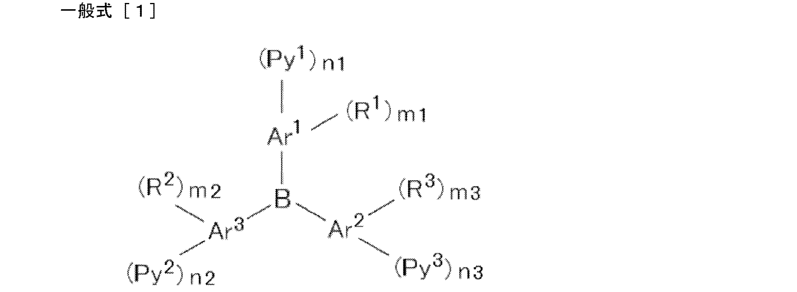
一般式[1]におけるR1、R2およびR3は、各々独立に、置換もしくは無置換のアルキル基、または置換もしくは無置換のアルコキシ基を表す。R1、R2およびR3は同一であっても異なっていてもよいが、好ましいのは同一である場合である。R1、R2およびR3は、それぞれAr1、Ar2およびAr3の芳香族炭化水素環の置換基として環に結合するものである。
R1、R2およびR3がとりうるアルキル基は、直鎖状であっても、分枝状であっても、環状であってもよい。好ましいのは直鎖状または分枝状のアルキル基である。アルキル基の炭素数は、1~20であることが好ましく、1~12であることがより好ましく、1~6であることがさらに好ましく、1~3であること(すなわちメチル基、エチル基、n-プロピル基、イソプロピル基)がさらにより好ましい。環状のアルキル基としては、例えばシクロペンチル基、シクロヘキシル基、シクロヘプチル基を挙げることができる。R1、R2およびR3がとりうるアルキル基は置換されていてもよく、その場合の置換基としてはアルコキシ基、アリール基、アリールオキシ基を挙げることができる。ここでいうアルコキシ基の説明と好ましい範囲については、下記のR1、R2およびR3がとりうるアルコキシ基の記載を参照することができる。ここでいうアリール基は、1つの芳香環からなるものであってもよいし、2以上の芳香環が融合した構造を有するものであってもよい。アリール基の環骨格構成炭素数は、6~22であることが好ましく、6~18であることがより好ましく、6~14であることがさらに好ましく、6~10であること(すなわちフェニル基、1-ナフチル基、2-ナフチル基)がさらにより好ましい。また、ここでいうアリールオキシ基は、1つの芳香環からなるものであってもよいし、2以上の芳香環が融合した構造を有するものであってもよい。アリールオキシ基の環骨格構成炭素数は、6~22であることが好ましく、6~18であることがより好ましく、6~14であることがさらに好ましく、6~10であること(すなわちフェニルオキシ基、1-ナフチルオキシ基、2-ナフチルオキシ基)がさらにより好ましい。
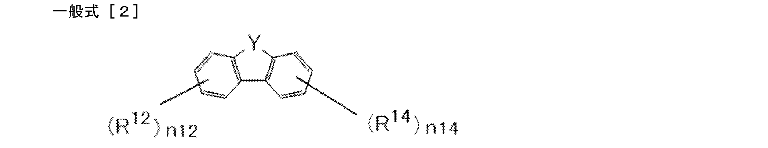


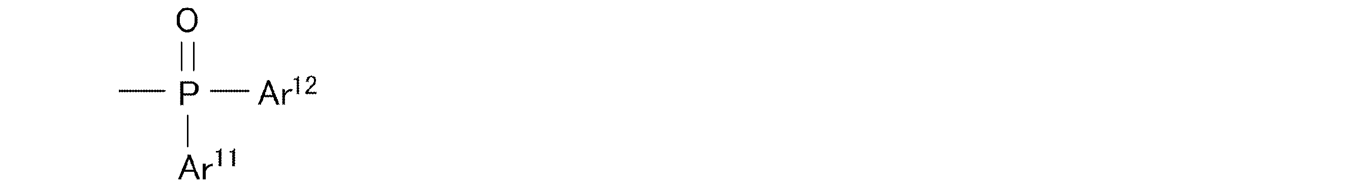


一般式[4]におけるPy31、Py32およびPy33は、各々独立に、置換もしくは無置換ピリジル基を表す。Py31、Py32およびPy33は同一であっても異なっていてもよいが、同一であることが好ましい。ここでいう置換もしくは無置換ピリジル基の説明と好ましい範囲については、一般式[1]の対応する記載を参照することができる。
一般式[4]におけるn31、n32およびn33は、各々独立に、1~3のいずれかの整数を表し、1または2であることが好ましい。例えば2,4,6位の3置換体、3,5位の2置換体、3位の1置換体、4位の1置換体を挙げることができる。n31、n32およびn33は同一であっても異なっていてもよいが、同一であることが好ましい。n31が2以上であるとき、分子内に存在する複数の(L31-Py31)は互いに同一であっても異なっていてもよい。好ましいのは同一である場合である。n32およびn33についても同じである。
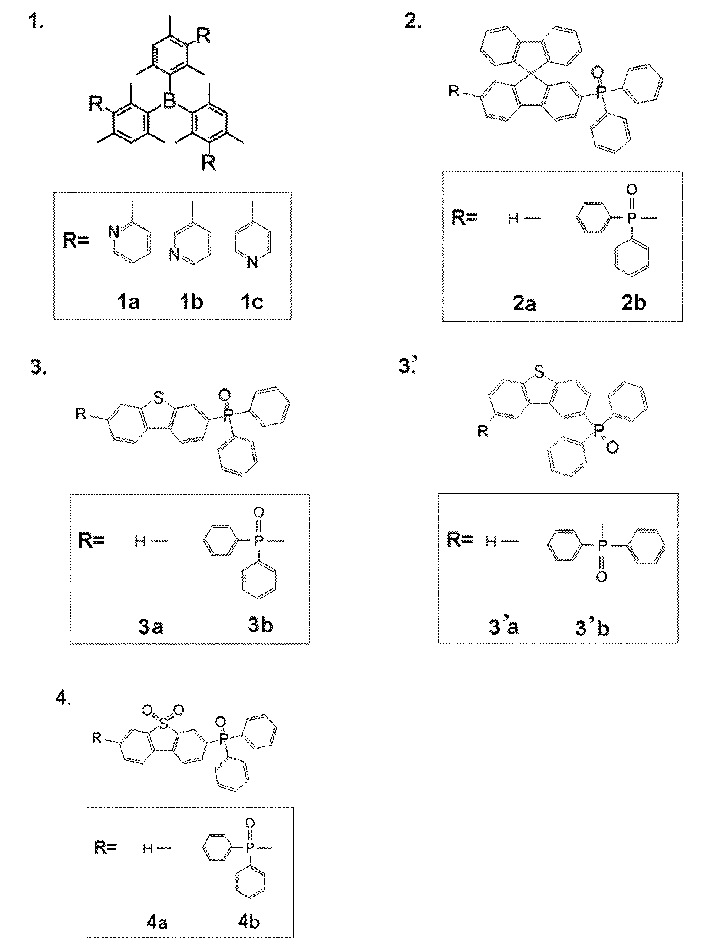
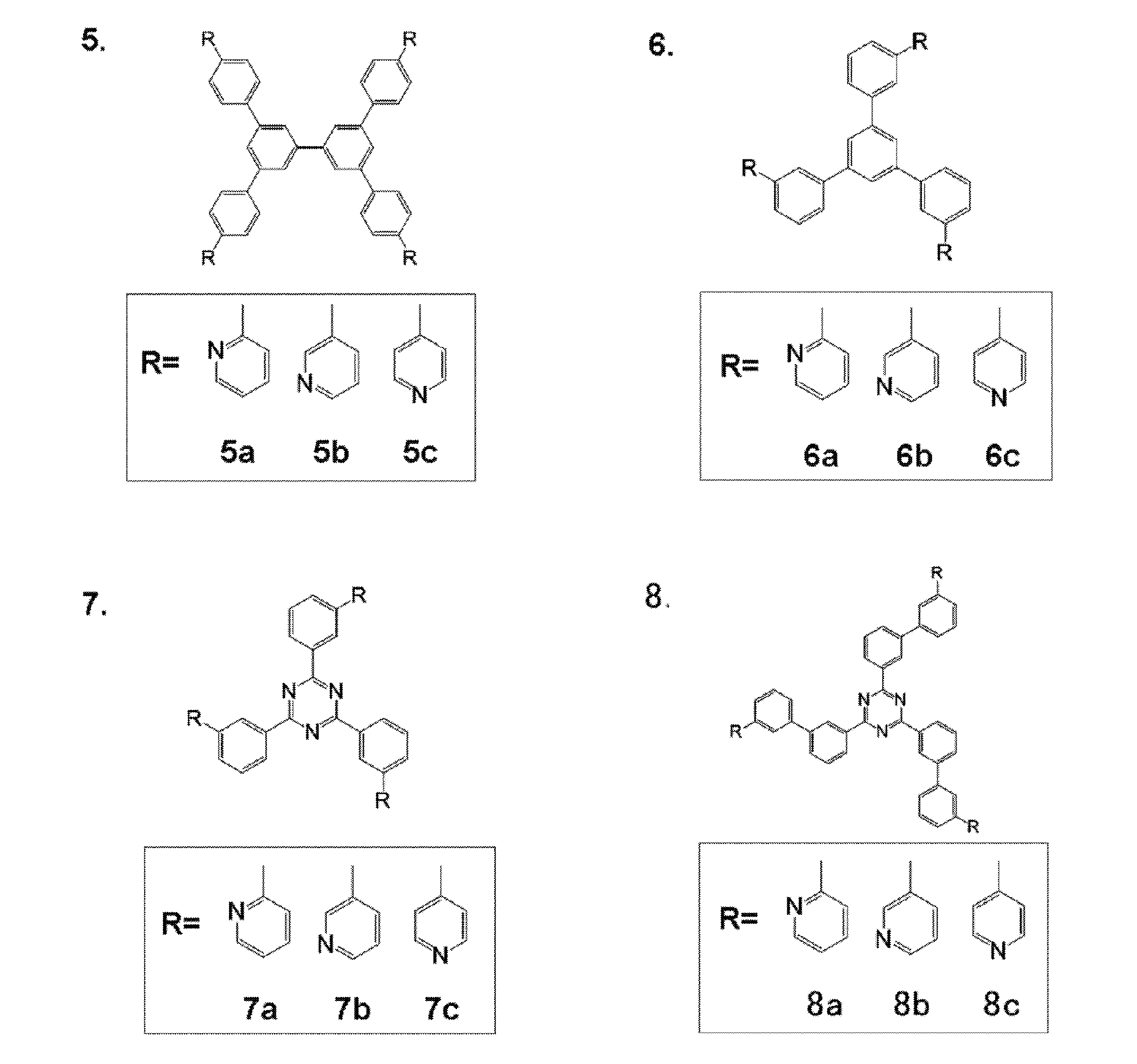
エキサイプレックス層に用いるドナー化合物は、式(5)と式(6)の条件を満たす化合物であることが好ましい。すなわち、ドナー化合物のリン光スペクトルにおける短波長側のピーク波長で規定される励起三重項エネルギー(T1 D)が、エキサイプレックス発光のピーク波長で規定されるエキサイプレックスの励起一重項エネルギー(S1)よりも大きくて、その差が0.2eV以上であることが好ましい。ドナー化合物の励起三重項エネルギー(T1 D)とエキサイプレックスの励起一重項エネルギー(S1)の差は、0.3eV超であることがより好ましく、0.4eV超であることがさらに好ましい。また、ドナー化合物のHOMOのエネルギー準位(|HOMOD|)は5.3eV以下であることが好ましく、5.2eV未満であることがより好ましく、5.1eV未満であることがさらに好ましい。
式(5) T1 D-S1 ≧ 0.2eV
式(6) |HOMOD| ≦ 5.3eV


一般式[12]におけるm61、m62およびm63は、各々独立に、1または2のいずれかを表す。例えば、3,5位の2置換体、3位の1置換体、4位の1置換体を挙げることができる。m61が2以上であるとき、分子内に存在する複数の

一般式[12]におけるn61、n62、n63、n64、n65およびn66は、各々独立に、0~5のいずれかの整数を表す。好ましいのは0~3のいずれかの整数であり、より好ましいのは0~2のいずれかの整数である。例えば、2,4,6位の3置換体、3,5位の2置換体、2位の1置換体、3位の1置換体、4位の1置換体を挙げることができる。n61が2以上であるとき、分子内に存在する複数のR61は互いに同一であっても異なっていてもよい。好ましいのは同一である場合である。また、分子内に存在する複数のR61のうちの2つのR61がベンゼン環の隣り合う炭素原子に結合しているとき、当該2つのR61は互いに結合して連結基を形成していてもよい。当該2つのR61が互いに結合して連結基を形成することにより、ベンゼン環に融合した環が形成される。2つのR61が互いに結合して形成する連結基の連結鎖原子数は3~5であることが好ましく、3または4であることがより好ましい。連結基としては、例えばアルキレン基、アルケニレン基を例示することができる。好ましい具体例として-CH=CH-CH=CH-や、その4つの水素原子の少なくとも1つが置換もしくは無置換のアルキル基、または置換もしくは無置換のアルコキシ基で置換された連結基を挙げることができる。ここでいう置換もしくは無置換のアルキル基と、置換もしくは無置換のアルコキシ基の説明と好ましい範囲については、一般式[1]の対応する記載を参照することができる。n61に関する上記説明は、n62、n63、n64、n65およびn66についても同じである。n61、n62、n63、n64、n65およびn66は同一であっても異なっていてもよいが、同一であることが好ましい。
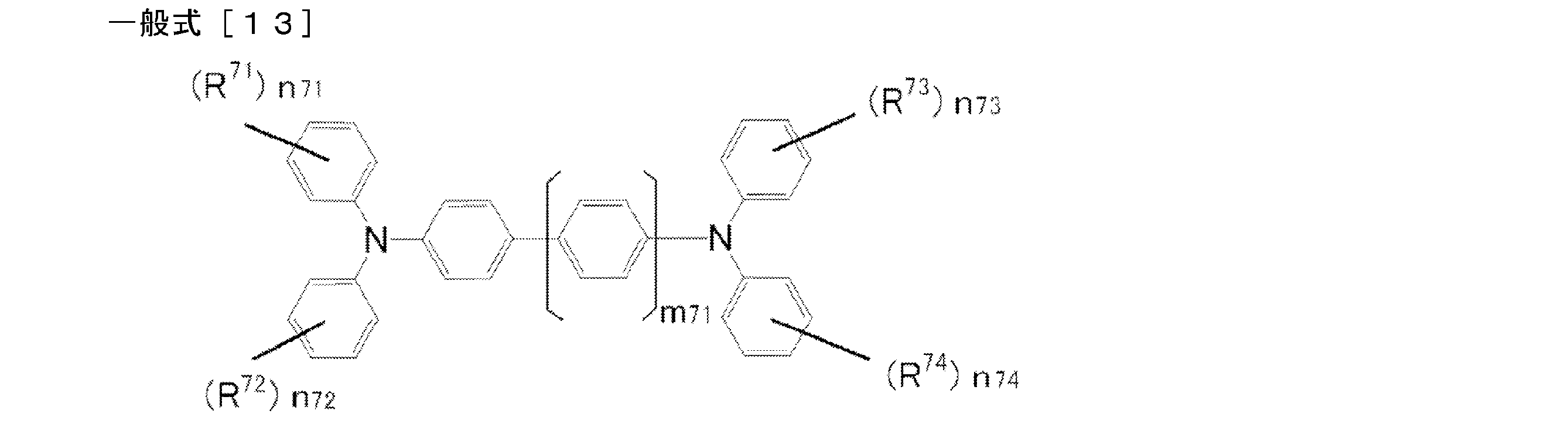

一般式[13]におけるn71、n72、n73、n74、n75およびn76は、各々独立に、0~5のいずれかの整数を表す。好ましくは0~3のいずれかの整数であり、より好ましくは0~2のいずれかの整数である。例えば、2,4,6位の3置換体、3,5位の2置換体、2位の1置換体、3位の1置換体、4位の1置換体を挙げることができる。n71が2以上であるとき、分子内に存在する複数のR71は互いに同一であっても異なっていてもよい。好ましいのは同一である場合である。また、分子内に存在する複数のR71のうちの2つのR71がベンゼン環の隣り合う炭素原子に結合しているとき、当該2つのR71は互いに結合して連結基を形成していてもよい。当該2つのR71が互いに結合して連結基を形成することにより、ベンゼン環に融合した環が形成される。2つのR71が互いに結合して形成する連結基の連結鎖原子数は3~5であることが好ましく、3または4であることがより好ましい。連結基としては、例えばアルキレン基、アルケニレン基を例示することができる。好ましい具体例として-CH=CH-CH=CH-や、その4つの水素原子の少なくとも1つが置換もしくは無置換のアルキル基、または置換もしくは無置換のアルコキシ基で置換された連結基を挙げることができる。ここでいう置換もしくは無置換のアルキル基と、置換もしくは無置換のアルコキシ基の説明と好ましい範囲については、一般式[1]の対応する記載を参照することができる。n71に関する上記説明は、n72、n73、n74、n75およびn76についても同じである。n71、n72、n73およびn74は同一であっても異なっていてもよいが、同一であることが好ましい。また、n75およびn76は同一であっても異なっていてもよいが、同一であることが好ましい。


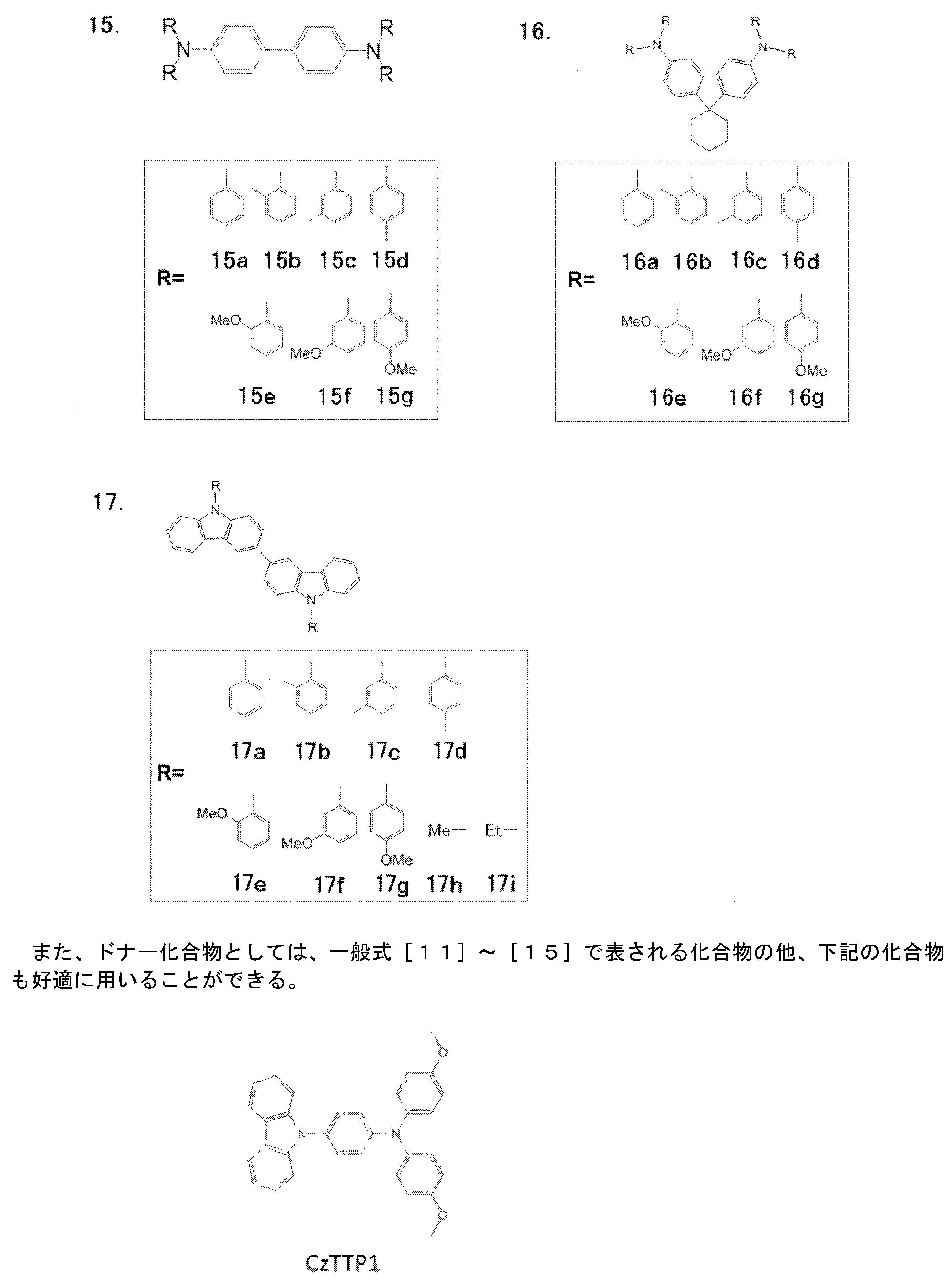
本発明では、アクセプター化合物とドナー化合物を混合して混合物とする。混合物中のドナー化合物のモル含有率(ドナー化合物/アクセプター化合物とドナー化合物の和)は、0.2超0.6未満であることが好ましく、0.3超0.6未満であることがより好ましく、0.4超0.6未満であることがさらにより好ましい。
アクセプター化合物とドナー化合物の組み合わせは、エキサイプレックスを形成することができるものであれば特に制限されない。以下の表にアクセプター化合物とドナー化合物の好ましい組み合わせを例示する。特に好ましい組み合わせ例として、下記の1、3、8、11、18、37、38を挙げることができ、より好ましくは37(ドナー化合物:TTP、アクセプター化合物:PPT)、38(ドナー化合物:dPTBdA、アクセプター化合物:PPT)である。さらに、ドナー化合物:CzTTP1とアクセプター化合物:PPTとの組合せも好適に用いることができる。31の遅延蛍光エキサイプレックス層は、一重項励起子生成効率が65~100%と高く、発光層の発光材料を効率よく蛍光発光させることができる。また、32、およびCzTTP1とPPTとの組合せの遅延エキサイプレックス層は、励起三重項エネルギーのデクスター移動が生じ難いため、後述する三重項励起子ブロッキング層が不要であり、有機エレクトロルミネッセンス素子の構成を単純にできるという効果がある。
遅延蛍光エキサイプレックス層の形成方法は特に制限されないが、例えば共蒸着法などを挙げる。

遅延蛍光エキサイプレックス層の厚さは、特に制限されないが10~120nmであることが好ましく、10~60nmであることがより好ましく、10~30nmであることがさらに好ましい。遅延蛍光エキサイプレックス層の厚さを上記範囲から選択することにより、一重項励起子生成効率の高い遅延蛍光エキサイプレックス層を得ることができる。
発光層は、発光材料を含み、遅延蛍光エキサイプレックス層からのエネルギー移動によって発光材料が励起され、その後、基底状態に戻る際に発光する層である。なお、本発明では、発光層でも正孔と電子との再結合が生じ得る。発光層に含まれる発光材料の一部は、このような正孔と電子との再結合によって励起され、その後、基底状態に戻る際に発光してもよい。
発光層と遅延蛍光エキサイプレックス層との位置関係は、遅延蛍光エキサイプレックス層が発光層よりも陰極側であってもよいし、陽極側であってもよい。
発光層に用いる発光材料は、蛍光材料であることが好ましい。これにより、遅延蛍光エキサイプレックス層で効率よく生成される一重項励起子を、発光材料の発光に有効に寄与させることができ、高発光効率の有機エレクトロルミネッセンス素子を実現することができる。また、蛍光材料として、遅延蛍光材料を使用してもよい。遅延蛍光材料は、キャリアの再結合によって励起一重項状態および励起三重項状態に励起されるが、励起三重項状態に励起されたとき、その少なくとも一部が逆項間交差により励起一重項状態に遷移する蛍光発光材料である。この場合、発光層の発光は、蛍光発光(即時蛍光)および遅延蛍光発光の両方を含む。


発光層は、発光材料単独で構成されていてもよいが、発光材料をゲスト化合物とするホスト化合物を含むことが好ましい。ホスト化合物としては、遅延蛍光エキサイプレックス層に含まれるドナー化合物およびアクセプター化合物と、発光材料であるゲスト化合物との間で、下記式(1)の条件を満たす有機化合物を用いることができる。
式(1) ES1>ES1 G かつ ES1 H>ES1 G
[式(1)において、ES1はドナー化合物とアクセプター化合物とで形成されるエキサイプレックスの最低励起一重項エネルギー準位を表し、ES1 Hはホスト化合物の最低励起一重項エネルギー準位を表し、ES1 Gはゲスト化合物の最低励起一重項エネルギー準位を表す。]
本発明における「最低励起一重項エネルギー準位」は、以下の方法により測定することができる。以下の方法では、測定対象化合物とmCBPを用いた場合について説明する。
測定対象化合物とmCBPとを、測定対象化合物が濃度6重量%となるように共蒸着することでSi基板上に厚さ100nmの試料を作製する。常温(300K)でこの試料の蛍光スペクトルを測定する。励起光入射直後から入射後100ナノ秒までの発光を積算することで、縦軸を燐光強度、横軸を波長の蛍光スペクトルを得る。蛍光スペクトルは、縦軸を発光、横軸を波長とする。この発光スペクトルの短波側のピーク波長値λを次に示す換算式でエネルギー値に換算した値をES1とする。
換算式:ES1[eV]=1239.85/λedge
発光スペクトルの測定には、励起光源に窒素レーザー(Lasertechnik Berlin社製、MNL200)を検出器には、ストリークカメラ(浜松ホトニクス社製、C4334)を用いることができる。
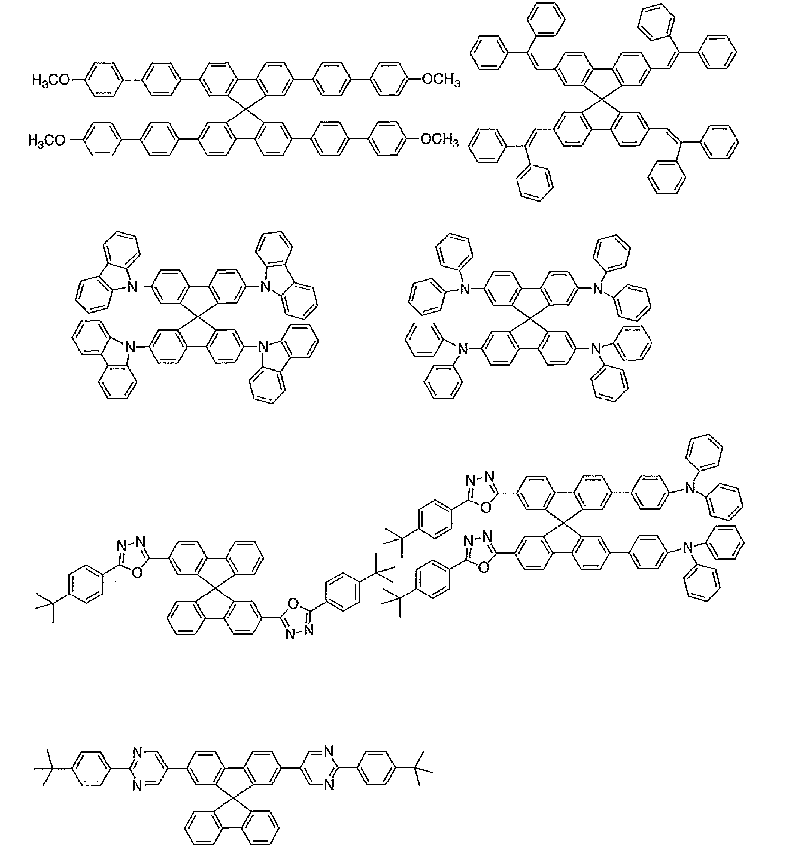

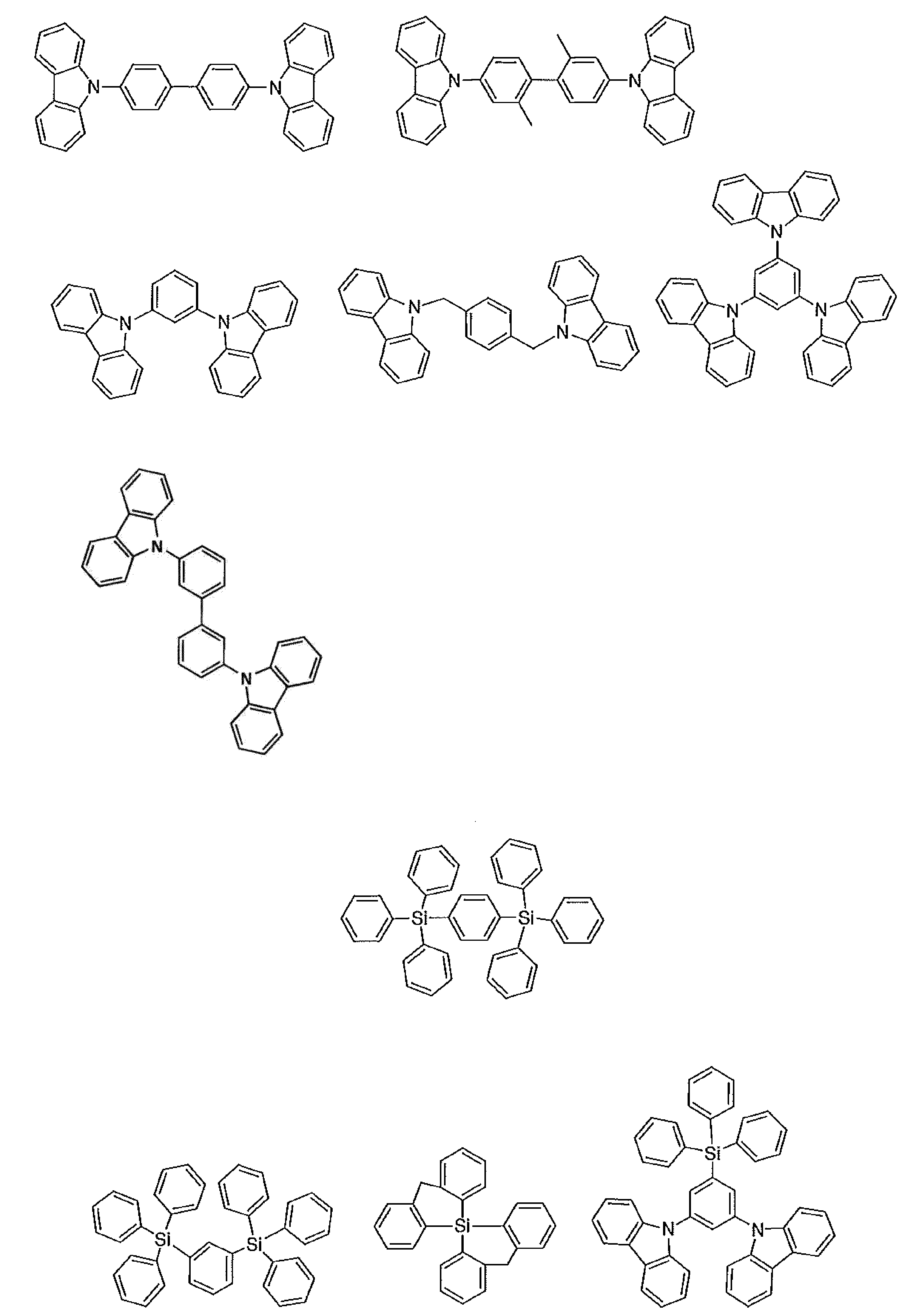

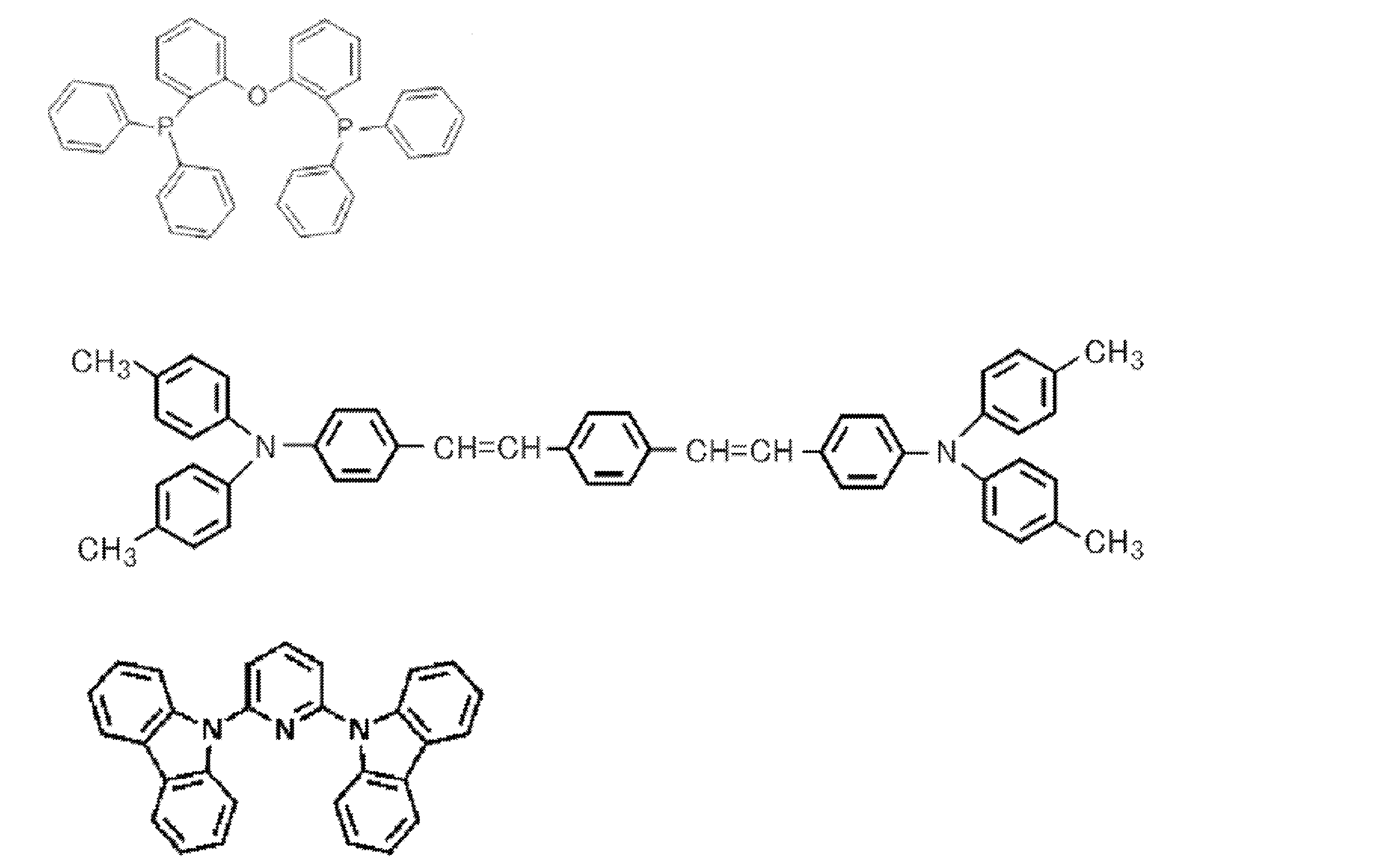
本発明の有機エレクトロルミネッセンス素子は、例えば実施例4のように、遅延蛍光エキサイプレックス層から発光層への励起三重項エネルギーのデクスター移動が頻繁に生じる系を採用した場合には、発光層と遅延蛍光エキサイプレックス層との間に三重項励起子ブロッキング層を設けることが好ましい。三重項励起子ブロッキング層は、遅延蛍光エキサイプレックス層から発光層への励起三重項エネルギーの移動を抑制する機能を有する。この三重項励起子ブロッキング層を設けることにより、以下の理由から有機エレクトロルミネッセンス素子の発光効率をより高めることができる。
すなわち、上記のように、遅延蛍光エキサイプレックス層では、励起三重項状態から励起一重項状態への逆項間交差が生じるが、逆項間交差が生じるよりも前に、励起三重項状態が隣接する有機層にエネルギー移動する場合がある。この場合に、遅延蛍光エキサイプレックス層からの励起三重項エネルギーを発光層の発光材料が受け取ると、発光材料が発光せずに熱失活し、そのエネルギーが無駄になってしまう。これに対して、発光層と遅延蛍光エキサイプレックス層との間に三重項励起子ブロッキング層を設けると、遅延蛍光エキサイプレックス層から発光層への励起三重項エネルギーの移動が抑えられ、遅延蛍光エキサイプレックス層で形成された励起三重項状態を確実に逆項間交差させ、蛍光発光に寄与させることができる。その結果、有機エレクトロルミネッセンス素子の発光効率をより高めることができる。
一方、遅延蛍光エキサイプックス層から発光層への励起三重項エネルギーのデクスター移動がさほど生じない系を採用した場合には、このような三重項励起子ブロッキング層の形成は不要であり、有機エレクトロルミネッセンス素子の構成を単純なものにすることができる。そのような遅延蛍光エキサイプレックス層としては、CzTTP1とPPTとの組み合わせ、dBTBdAとPPTとの組み合わせ等を挙げることができる。
三重項励起子ブロッキング層の構成材料としては、遅延蛍光エキサイプレックス層に含まれるドナー化合物およびアクセプター化合物と、発光層に含まれるホスト化合物およびゲスト化合物との間で、下記式(2)の条件を満たす有機化合物(ブロッキング化合物)を用いることが好ましい。
式(2) ET1 B>ET1>ET1 H>ET1 G
[式(2)において、ET1 Bはブロッキング化合物の最低励起三重項エネルギー準位を表し、ET1はドナー化合物とアクセプター化合物とで形成されるエキサイプレックスの最低励起三重項エネルギー準位を表し、ET1 Hはホスト化合物の最低励起三重項エネルギー準位を表し、ET1 Gはゲスト化合物の最低励起三重項エネルギー準位を表す。]
本発明における「最低励起三重項エネルギー準位」は、以下の方法により測定することができる。以下の方法では、測定対象化合物とmCBPを用いた場合について説明する。
上記の一重項エネルギーES1の測定に用いたのと同じ試料を5[K]に冷却し、励起光(337nm)を燐光測定用試料に照射し、ストリークカメラを用いて、燐光強度を測定する。励起光入射後1ミリ秒から入射後10ミリ秒の発光を積算することで、縦軸を燐光強度、横軸を波長の燐光スペクトルを得る。この発光スペクトルの短波側のピーク波長値λを次に示す換算式でエネルギー値に換算した値をES1とする。
換算式:ET1[eV]=1239.85/λedge

三重項励起子ブロッキング層の厚さは、遅延蛍光エキサイプレックス層のエキサイプレックスと発光層の発光材料との間のフェルスター移動半径をR0を考慮して選択することが好ましい。具体的には、三重項励起子ブロッキング層の膜厚が一般的なデクスタ―エネルギー移動距離である2nmより大きい十分大きくフェルスター移動半径より小さいことが望ましい。
ここで、フェルスター移動半径は、ゲスト化合物のモル吸光係数と遅延蛍光エキサイプレックスの発光スペクトルによって測定されるものである。
三重項励起子ブロッキング層の厚さを上記範囲から選択することにより、三重項励起子ブロッキング層の機能を十分に享受しつつ、発光層と遅延蛍光エキサイプレックス層との間隔をフェルスター機構によるエネルギー移動が可能な範囲に収めることができ、遅延蛍光エキサイプレックス層で生成した励起一重項エネルギーを発光層へ効率よく移動させることができる。
例えば、発光材料としてC545Tを用い、遅延蛍光エキサイプレックスのドナー化合物としてTTPを用い、遅延蛍光エキサイプレックス層のアクセプター化合物としてPPTを用いた場合のフェルスター移動半径R0は3.5nmである。これらと組み合わせてmCPをブロッキング化合物として用いる場合、三重項励起子ブロッキング層の厚さは、2~8nmであることが好ましく、3~5nmであることがさらに好ましく、3.5~4.5nmであることが最も好ましい。
本発明の有機エレクトロルミネッセンス素子は、遅延蛍光エキサイプレックス層、発光層、三重項励起子ブロッキング層の他に、以下のような有機層を有していてもよい。
(注入層)
注入層とは、駆動電圧低下や発光輝度向上のために電極と有機層間に設けられる層のことで、正孔注入層と電子注入層があり、陽極と発光層または正孔輸送層の間、および陰極と発光層または電子輸送層との間に存在させてもよい。注入層は必要に応じて設けることができる。
阻止層は、発光層中に存在する電荷(電子もしくは正孔)および/または励起子の発光層外への拡散を阻止することができる層である。電子阻止層は、発光層および正孔輸送層の間に配置されることができ、電子が正孔輸送層の方に向かって発光層を通過することを阻止する。同様に、正孔阻止層は発光層および電子輸送層の間に配置されることができ、正孔が電子輸送層の方に向かって発光層を通過することを阻止する。阻止層はまた、励起子が発光層の外側に拡散することを阻止するために用いることができる。すなわち電子阻止層、正孔阻止層はそれぞれ励起子阻止層としての機能も兼ね備えることができる。本明細書でいう電子阻止層または励起子阻止層は、一つの層で電子阻止層および励起子阻止層の機能を有する層を含む意味で使用される。
正孔阻止層とは広い意味では電子輸送層の機能を有する。正孔阻止層は電子を輸送しつつ、正孔が電子輸送層へ到達することを阻止する役割があり、これにより発光層中での電子と正孔の再結合確率を向上させることができる。正孔阻止層の材料としては、後述する電子輸送層の材料を必要に応じて用いることができる。
電子阻止層とは、広い意味では正孔を輸送する機能を有する。電子阻止層は正孔を輸送しつつ、電子が正孔輸送層へ到達することを阻止する役割があり、これにより発光層中での電子と正孔が再結合する確率を向上させることができる。
励起子阻止層とは、発光層内で正孔と電子が再結合することにより生じた励起子が電荷輸送層に拡散することを阻止するための層であり、本層の挿入により励起子を効率的に発光層内に閉じ込めることが可能となり、素子の発光効率を向上させることができる。励起子阻止層は発光層に隣接して陽極側、陰極側のいずれにも挿入することができ、両方同時に挿入することも可能である。すなわち、励起子阻止層を陽極側に有する場合、正孔輸送層と発光層の間に、発光層に隣接して該層を挿入することができ、陰極側に挿入する場合、発光層と陰極との間に、発光層に隣接して該層を挿入することができる。また、陽極と、発光層の陽極側に隣接する励起子阻止層との間には、正孔注入層や電子阻止層などを有することができ、陰極と、発光層の陰極側に隣接する励起子阻止層との間には、電子注入層、電子輸送層、正孔阻止層などを有することができる。阻止層を配置する場合、阻止層として用いる材料の励起一重項エネルギーおよび励起三重項エネルギーの少なくともいずれか一方は、発光材料の励起一重項エネルギーおよび励起三重項エネルギーよりも高いことが好ましい。
正孔輸送層とは正孔を輸送する機能を有する正孔輸送材料からなり、正孔輸送層は単層または複数層設けることができる。
正孔輸送材料としては、正孔の注入または輸送、電子の障壁性のいずれかを有するものであり、有機物、無機物のいずれであってもよい。使用できる公知の正孔輸送材料としては例えば、トリアゾール誘導体、オキサジアゾール誘導体、イミダゾール誘導体、カルバゾール誘導体、インドロカルバゾール誘導体、ポリアリールアルカン誘導体、ピラゾリン誘導体およびピラゾロン誘導体、フェニレンジアミン誘導体、アリールアミン誘導体、アミノ置換カルコン誘導体、オキサゾール誘導体、スチリルアントラセン誘導体、フルオレノン誘導体、ヒドラゾン誘導体、スチルベン誘導体、シラザン誘導体、アニリン系共重合体、また導電性高分子オリゴマー、特にチオフェンオリゴマー等が挙げられるが、ポルフィリン化合物、芳香族第3級アミン化合物およびスチリルアミン化合物を用いることが好ましく、芳香族第3級アミン化合物を用いることがより好ましい。
電子輸送層とは電子を輸送する機能を有する材料からなり、電子輸送層は単層または複数層設けることができる。
電子輸送材料(正孔阻止材料を兼ねる場合もある)としては、陰極より注入された電子を発光層に伝達する機能を有していればよい。使用できる電子輸送層としては例えば、ニトロ置換フルオレン誘導体、ジフェニルキノン誘導体、チオピランジオキシド誘導体、カルボジイミド、フレオレニリデンメタン誘導体、アントラキノジメタンおよびアントロン誘導体、オキサジアゾール誘導体等が挙げられる。さらに、上記オキサジアゾール誘導体において、オキサジアゾール環の酸素原子を硫黄原子に置換したチアジアゾール誘導体、電子吸引基として知られているキノキサリン環を有するキノキサリン誘導体も、電子輸送材料として用いることができる。さらにこれらの材料を高分子鎖に導入した、またはこれらの材料を高分子の主鎖とした高分子材料を用いることもできる。


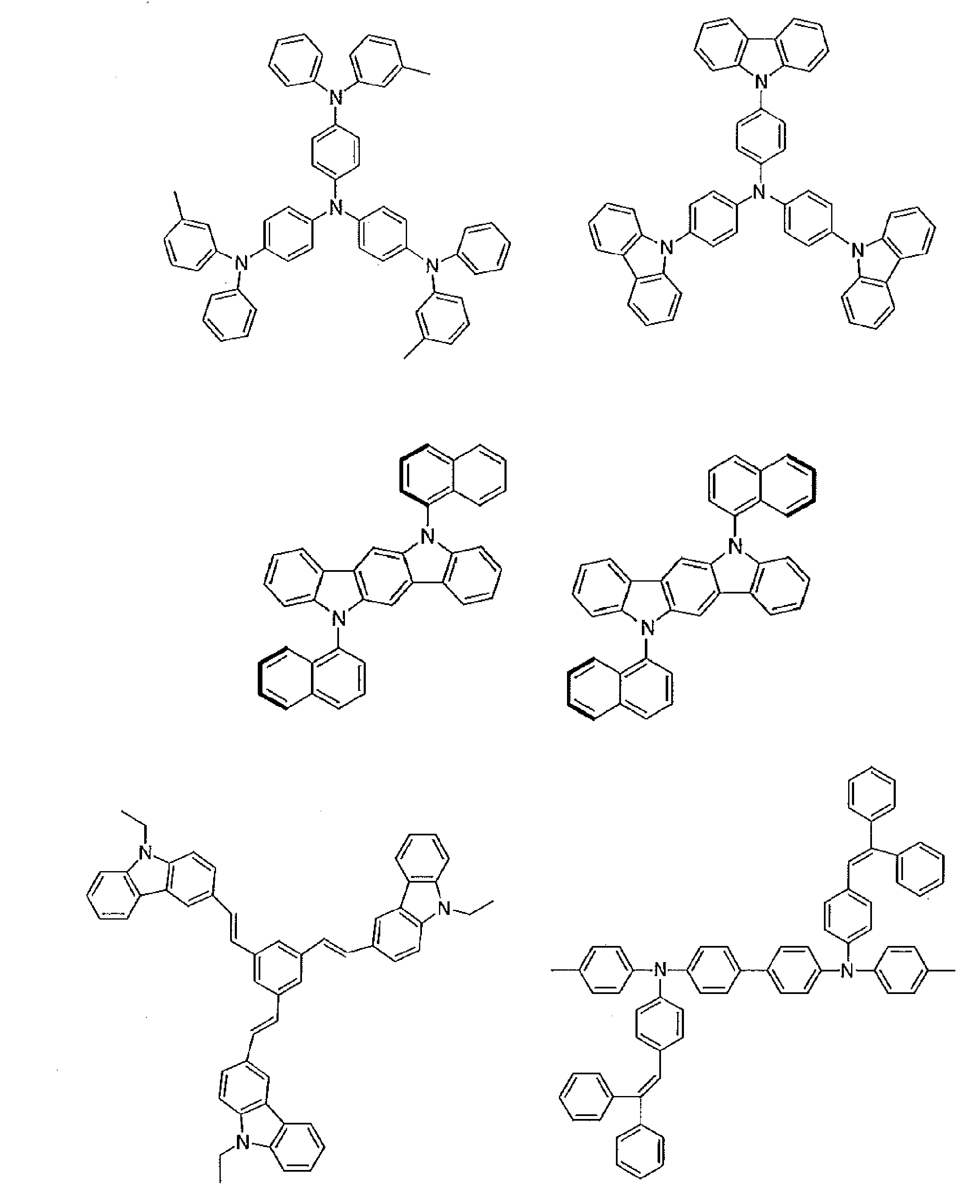


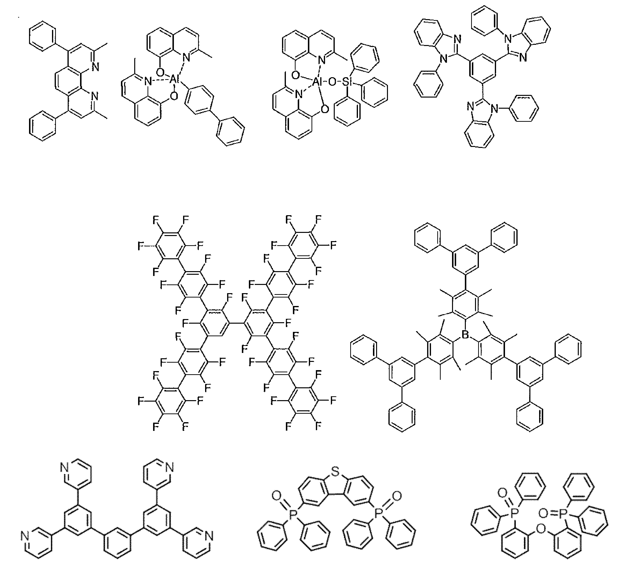


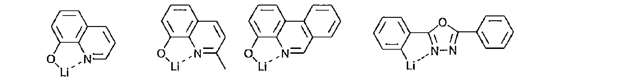

本発明の有機エレクトロルミネッセンス素子は、基板に支持されていることが好ましい。この基板については、特に制限はなく、従来から有機エレクトロルミネッセンス素子に慣用されているものであればよく、例えば、ガラス、透明プラスチック、石英、シリコンなどからなるものを用いることができる。
有機エレクトロルミネッセンス素子における陽極としては、仕事関数の大きい(4eV以上)金属、合金、電気伝導性化合物およびこれらの混合物を電極材料とするものが好ましく用いられる。このような電極材料の具体例としてはAu等の金属、CuI、インジウムチンオキシド(ITO)、SnO2、ZnO等の導電性透明材料が挙げられる。また、IDIXO(In2O3-ZnO)等非晶質で透明導電膜を作製可能な材料を用いてもよい。陽極はこれらの電極材料を蒸着やスパッタリング等の方法により、薄膜を形成させ、フォトリソグラフィー法で所望の形状のパターンを形成してもよく、あるいはパターン精度をあまり必要としない場合は(100μm以上程度)、上記電極材料の蒸着やスパッタリング時に所望の形状のマスクを介してパターンを形成してもよい。あるいは、有機導電性化合物のように塗布可能な材料を用いる場合には、印刷方式、コーティング方式等湿式成膜法を用いることもできる。この陽極より発光を取り出す場合には、透過率を10%より大きくすることが望ましく、また陽極としてのシート抵抗は数百Ω/□以下が好ましい。さらに膜厚は材料にもよるが、通常10~1000nm、好ましくは10~200nmの範囲で選ばれる。
一方、陰極としては、仕事関数の小さい(4eV以下)金属(電子注入性金属と称する)、合金、電気伝導性化合物およびこれらの混合物を電極材料とするものが用いられる。このような電極材料の具体例としては、ナトリウム、ナトリウム-カリウム合金、マグネシウム、リチウム、マグネシウム/銅混合物、マグネシウム/銀混合物、マグネシウム/アルミニウム混合物、マグネシウム/インジウム混合物、アルミニウム/酸化アルミニウム(Al2O3)混合物、インジウム、リチウム/アルミニウム混合物、希土類金属等が挙げられる。これらの中で、電子注入性および酸化等に対する耐久性の点から、電子注入性金属とこれより仕事関数の値が大きく安定な金属である第二金属との混合物、例えば、マグネシウム/銀混合物、マグネシウム/アルミニウム混合物、マグネシウム/インジウム混合物、アルミニウム/酸化アルミニウム(Al2O3)混合物、リチウム/アルミニウム混合物、アルミニウム等が好適である。陰極はこれらの電極材料を蒸着やスパッタリング等の方法により薄膜を形成させることにより、作製することができる。また、陰極としてのシート抵抗は数百Ω/□以下が好ましく、膜厚は通常10nm~5μm、好ましくは50~200nmの範囲で選ばれる。なお、発光した光を透過させるため、有機エレクトロルミネッセンス素子の陽極または陰極のいずれか一方が、透明または半透明であれば発光輝度が向上し好都合である。
また、陽極の説明で挙げた導電性透明材料を陰極に用いることで、透明または半透明の陰極を作製することができ、これを応用することで陽極と陰極の両方が透過性を有する素子を作製することができる。
膜厚100nmのインジウム・スズ酸化物(ITO)からなる陽極が形成されたガラス基板を用意した。このガラス基板の陽極上に、CzTTP1を35nmの厚さに形成して正孔輸送層を得た。次に、CzTTP1とPPTとを異なる蒸着源から共蒸着し、30nmの厚さの層を形成して遅延蛍光エキサイプレックス層とした。この時、CzTTP1の濃度は30mol%とした。次に、C545TとPPTとを異なる蒸着源から共蒸着し、10nmの厚さの層を形成して発光層とした。この時、C545Tの濃度は1重量%とした。次に、PPTを25nmの厚さに形成して電子輸送層を得た。さらに、フッ化リチウム(LiF)を0.8nmの厚さに蒸着し、次いでアルミニウム(Al)を80nmの厚さに蒸着することにより陰極を形成し、有機エレクトロルミネッセンス素子とした。
正孔輸送層の材料および遅延蛍光エキサイプレックス層のドナー化合物としてCzTTP1の代わりにdPTBdAを用いたこと以外は、実施例1と同様にして有機エレクトロルミネッセンス素子を作製した。
遅延エキサイプレックス層のdPTBdAの濃度を50mol%としたこと以外は、実施例2と同様にして有機エレクトロルミネッセンス素子を作製した。
(三重項励起子ブロッキング層の膜厚の検討)
本実施例では、発光層(C545T-CBP蒸着膜)と遅延蛍光エキサイプレックス層(TTP-PPT蒸着膜)との間に三重項励起子ブロッキング層(mCP蒸着膜)を形成するため、予備実験として三重項励起子ブロッキング層の膜厚を検討した。
(1)遅延蛍光エキサイプレックス層と発光層とのフェルスター移動半径R0
図2に、TTPとPPTとを50mol%で共蒸着したTTP-PPT蒸着膜の発光スペクトルと、C545Tのトルエン溶液の吸収スペクトルを併せて示す。図2から、TTP-PPT蒸着膜とC454Tとのフェルスター移動半径R0は3.5nmであり、三重項励起子ブロッキング層の厚さの上限は(3.5+1)nm付近であることが推定された。
ガラス基板上に、α-NPDを10nmの厚さに形成した。次に、C545TとCBPとを異なる蒸着源から共蒸着し、10nmの厚さの層を形成して発光層とした。この時、C545Tの濃度は2.5重量%とした。次に、mCPを0~8nmから選択した各種厚さで形成し、mCP膜を得た。次に、TTPとPPTとを異なる蒸着源から共蒸着し、10nmの厚さの層を形成して遅延蛍光エキサイプレックス層とした。この時、TTPおよびPPTの濃度は50mol%とした。以上の工程により、mCP膜の厚さが異なる各サンプルを作製した。
作成した各サンプルについて、遅延蛍光スペクトルを図3に示し、PL量子収率をmCP膜の厚さに対してプロットした結果を図4に示す。
また、図4を見ると、PL量子収率は、mCP膜が4nmのサンプルが最も高く、mCP膜を2nm、6nm、8nmで形成したサンプルは、mCP膜を形成していないサンプルに比べれば高い値が得られるものの、mCP膜を4nmで形成したサンプルよりも低い値になっている。このことから、mCP膜の厚さは、2~8nmであることが好ましく、4nmであることが最適であることがわかった。
厚さ4nmのmCP膜を三重項励起子ブロッキング層とする有機エレクトロルミネッセンス素子を次にようにして作製した。
膜厚100nmのインジウム・スズ酸化物膜(ITO膜)および膜厚1nmのMoOx膜からなる陽極が形成されたガラス基板を用意した。このガラス基板の陽極上に、α-NPDを40nmの厚さに形成して正孔輸送層を得た。次に、C545TとCBPとを異なる蒸着源から共蒸着し、10nmの厚さの層を形成して発光層とした。この時、C545Tの濃度は2.5重量%とした。次に、mCPを4nmの厚さに形成し、三重項励起子ブロッキング層を得た。次に、TTPとPPTとを異なる蒸着源から共蒸着し、30nmの厚さの層を形成して遅延蛍光エキサイプレックス層とした。この時、TTPの濃度は50mol%とした。次に、PPTを40nmの厚さに形成して電子輸送層を得た。さらに、フッ化リチウム(LiF)を0.75nmの厚さに蒸着し、次いでアルミニウム(Al)を70nmの厚さに蒸着することにより陰極を形成し、有機エレクトロルミネッセンス素子とした。
膜厚100nmのインジウム・スズ酸化物(ITO)からなる陽極が形成されたガラス基板を用意した。このガラス基板の陽極上に、TTPを20nmの厚さに形成して正孔輸送層を得た。次に、TTPとPPTとを異なる蒸着源から共蒸着し、60nmの厚さの層を形成して発光層とした。この時、TTPの濃度は50mol%とした。次に、PPTを20nmの厚さに形成して電子輸送層を得た。さらに、フッ化リチウム(LiF)を0.75nmの厚さに蒸着し、次いでアルミニウム(Al)を70nmの厚さに蒸着することにより陰極を形成し、有機エレクトロルミネッセンス素子とした。
(1)発光材料の発光特性
図5に、C545Tのトルエン溶液の発光スペクトルおよび吸収スペクトルを示す。C545Tのトルエン溶液のPL量子収率は91.3%であった。
(2)遅延蛍光エキサイプレックス層の発光特性
代表として、図6に、TTPとPPTとを50mol%で共蒸着したTTP-PPT蒸着膜、TTP蒸着膜、PPT蒸着膜の発光スペクトルを併せて示し、図7に、TTP-PPT蒸着膜の過渡減衰曲線を示す。TTP-PPT蒸着膜のPL量子収率は15.6%であり、このうち遅延蛍光成分のPL量子収率は12.3%であった。また、後述する比較例1の外部量子効率の測定結果から求めた、TTP-PPT蒸着膜の一重項励起子生成効率は65~100%であった。
作製した各有機エレクトロルミネッセンス素子について、電流密度-外部量子効率特性を図8~図12に示し、最大外部量子効率を表3に示す。なお図11では、遅延蛍光エキサイプレックス層の厚さを10nmに変更した素子を測定した結果も掲載している。


2 陽極
3 正孔注入層
4 正孔輸送層
5 発光層
6 三重項励起子ブロッキング層
7 遅延蛍光エキサイプレックス層
8 電子輸送層
9 陰極
Claims (8)
- 発光層と、ドナー化合物およびアクセプター化合物を含有する遅延蛍光エキサイプレックス層とを含む少なくとも2層の有機層を一対の電極間に有することを特徴とする有機エレクトロルミネッセンス素子。
- 前記発光層は、ホスト化合物および発光材料であるゲスト化合物を含み、
前記ホスト化合物および前記ゲスト化合物と、前記ドナー化合物および前記アクセプター化合物とが、下記式(1)で表される条件を満たすことを特徴とする請求項1に記載の有機エレクトロルミネッセンス素子。
式(1) ES1>ES1 G かつ ES1 H>ES1 G
[式(1)において、ES1はドナー化合物とアクセプター化合物とで形成されるエキサイプレックスの最低励起一重項エネルギー準位を表し、ES1 Hはホスト化合物の最低励起一重項エネルギー準位を表し、ES1 Gはゲスト化合物の最低励起一重項エネルギー準位を表す。] - 前記有機層は、前記発光層と前記遅延蛍光エキサイプレックス層との間に、前記遅延蛍光エキサイプレックス層から前記発光層への励起三重項エネルギーの移動を抑制する三重項励起子ブロッキング層を有することを特徴とする請求項1又は2に記載の有機エレクトロルミネッセンス素子。
- 前記三重項励起子ブロッキング層は、前記ホスト化合物および前記ゲスト化合物と、前記ドナー化合物および前記アクセプター化合物との間で、下記式(2)で表される条件を満たすブロッキング化合物を含むことを特徴とする請求項3に記載の有機エレクトロルミネッセンス素子。
式(2) ET1 B>ET1>ET1 H>ET1 G
[式(2)において、ET1 Bはブロッキング化合物の最低励起三重項エネルギー準位を表し、ET1はドナー化合物とアクセプター化合物とで形成されるエキサイプレックスの最低励起三重項エネルギー準位を表し、ET1 Hはホスト化合物の最低励起三重項エネルギー準位を表し、ET1 Gはゲスト化合物の最低励起三重項エネルギー準位を表す。] - 前記三重項励起子ブロッキング層の膜厚が、2nm以上である請求項3または4に記載の有機エレクトロルミネッセンス素子。
- 前記三重項励起子ブロッキング層の膜厚が、2nm~8nmである請求項3~5のいずれか1項に記載の有機エレクトロルミネッセンス素子。
- 前記三重項励起子ブロッキング層の膜厚が、3.5~4.5nmである請求項3~6のいずれか1項に記載の有機エレクトロルミネッセンス素子。
- 前記発光層に含まれるゲスト化合物は、蛍光材料であることを特徴とする請求項2~7のいずれか1項に記載の有機エレクトロルミネッセンス素子。
Priority Applications (5)
| Application Number | Priority Date | Filing Date | Title |
|---|---|---|---|
| CN201480051330.1A CN105580153B (zh) | 2013-09-17 | 2014-09-12 | 有机电致发光元件 |
| KR1020167007793A KR102074031B1 (ko) | 2013-09-17 | 2014-09-12 | 유기 일렉트로루미네선스 소자 |
| JP2015537897A JP6470181B2 (ja) | 2013-09-17 | 2014-09-12 | 有機エレクトロルミネッセンス素子 |
| EP14846505.7A EP3059775B1 (en) | 2013-09-17 | 2014-09-12 | Organic electroluminescence element |
| US15/022,244 US10014487B2 (en) | 2013-09-17 | 2014-09-12 | Organic electroluminescent device |
Applications Claiming Priority (2)
| Application Number | Priority Date | Filing Date | Title |
|---|---|---|---|
| JP2013192357 | 2013-09-17 | ||
| JP2013-192357 | 2013-09-17 |
Publications (1)
| Publication Number | Publication Date |
|---|---|
| WO2015041157A1 true WO2015041157A1 (ja) | 2015-03-26 |
Family
ID=52688808
Family Applications (1)
| Application Number | Title | Priority Date | Filing Date |
|---|---|---|---|
| PCT/JP2014/074174 WO2015041157A1 (ja) | 2013-09-17 | 2014-09-12 | 有機エレクトロルミネッセンス素子 |
Country Status (7)
| Country | Link |
|---|---|
| US (1) | US10014487B2 (ja) |
| EP (1) | EP3059775B1 (ja) |
| JP (2) | JP6470181B2 (ja) |
| KR (1) | KR102074031B1 (ja) |
| CN (1) | CN105580153B (ja) |
| TW (1) | TWI640111B (ja) |
| WO (1) | WO2015041157A1 (ja) |
Cited By (15)
| Publication number | Priority date | Publication date | Assignee | Title |
|---|---|---|---|---|
| WO2016027760A1 (ja) * | 2014-08-22 | 2016-02-25 | シャープ株式会社 | 有機エレクトロルミネッセンス素子およびその製造方法並びに発光方法 |
| JP2016141647A (ja) * | 2015-02-02 | 2016-08-08 | 日本放送協会 | 化合物、有機エレクトロルミネッセンス素子、表示装置、照明装置、有機薄膜太陽電池 |
| KR20170026075A (ko) * | 2015-08-27 | 2017-03-08 | 삼성전자주식회사 | 박막 및 이를 포함한 유기 발광 소자 |
| EP3142162A1 (en) * | 2015-09-14 | 2017-03-15 | Samsung Electronics Co., Ltd. | Composition, thin film, and organic light emitting device including composition and thin film |
| KR20170032148A (ko) * | 2015-09-14 | 2017-03-22 | 삼성전자주식회사 | 혼합물, 박막 및 이를 포함한 유기 발광 소자 |
| JP2017126656A (ja) * | 2016-01-14 | 2017-07-20 | 国立大学法人九州大学 | 有機エレクトロルミネッセンス素子、素子群、有機エレクトロルミネッセンス素子の製造方法、有機エレクトロルミネッセンス素子の発光波長制御方法 |
| WO2018047853A1 (ja) * | 2016-09-06 | 2018-03-15 | 株式会社Kyulux | 有機発光素子 |
| JP6323970B1 (ja) * | 2016-12-06 | 2018-05-16 | 国立大学法人九州大学 | 蓄光体および蓄光素子 |
| CN108123047A (zh) * | 2016-11-30 | 2018-06-05 | 财团法人工业技术研究院 | 有机发光二极管和白光有机发光二极管 |
| WO2018105633A1 (ja) * | 2016-12-06 | 2018-06-14 | 国立大学法人九州大学 | 蓄光体および蓄光素子 |
| WO2018150450A1 (ja) * | 2017-02-14 | 2018-08-23 | コニカミノルタ株式会社 | アミノクマリン化合物およびアミノクマリン化合物内包樹脂粒子 |
| WO2018151072A1 (ja) * | 2017-02-14 | 2018-08-23 | コニカミノルタ株式会社 | アミノクマリン化合物およびアミノクマリン化合物内包樹脂粒子 |
| US10240085B2 (en) | 2015-08-27 | 2019-03-26 | Samsung Electronics Co., Ltd. | Thin film and organic light-emitting device including the same |
| WO2019189045A1 (ja) * | 2018-03-29 | 2019-10-03 | 国立大学法人九州大学 | 蓄光体および蓄光素子 |
| WO2021070797A1 (ja) * | 2019-10-10 | 2021-04-15 | 国立大学法人九州大学 | 組成物および有機発光素子 |
Families Citing this family (13)
| Publication number | Priority date | Publication date | Assignee | Title |
|---|---|---|---|---|
| US10014487B2 (en) * | 2013-09-17 | 2018-07-03 | Kyulux, Inc. | Organic electroluminescent device |
| WO2015107719A1 (ja) * | 2014-01-14 | 2015-07-23 | シャープ株式会社 | 有機エレクトロルミネッセンス表示パネル |
| TWI704706B (zh) * | 2015-03-09 | 2020-09-11 | 日商半導體能源研究所股份有限公司 | 發光元件、顯示裝置、電子裝置及照明設置 |
| TWI779405B (zh) * | 2015-03-09 | 2022-10-01 | 日商半導體能源研究所股份有限公司 | 發光元件,顯示裝置,電子裝置,與照明裝置 |
| CN106784354B (zh) * | 2016-12-29 | 2019-02-26 | 上海天马有机发光显示技术有限公司 | 有机发光显示器件及其制造方法、以及有机发光显示装置 |
| CN108336237B (zh) | 2017-01-20 | 2020-01-31 | 昆山工研院新型平板显示技术中心有限公司 | 一种有机电致发光器件 |
| KR102366420B1 (ko) * | 2017-07-31 | 2022-02-22 | 엘지디스플레이 주식회사 | 유기발광다이오드 및 이를 포함하는 유기발광 표시장치 |
| CN111836871A (zh) * | 2017-08-09 | 2020-10-27 | 学校法人冲绳科学技术大学院大学学园 | 长余辉组合物、长余辉元件及波长控制方法 |
| KR102497284B1 (ko) * | 2017-12-18 | 2023-02-08 | 삼성디스플레이 주식회사 | 유기 발광 소자 |
| CN108365112B (zh) * | 2018-01-19 | 2020-06-16 | 昆山国显光电有限公司 | 一种电致发光器件 |
| KR102634554B1 (ko) * | 2018-06-12 | 2024-02-06 | 엘지디스플레이 주식회사 | 공간 전하 이동 화합물, 이를 포함하는 유기발광다이오드 및 유기발광표시장치 |
| WO2020199191A1 (zh) * | 2019-04-04 | 2020-10-08 | 复旦大学 | 长余辉发光材料 |
| CN110783473B (zh) * | 2019-10-31 | 2022-10-21 | 昆山国显光电有限公司 | 一种发光器件和显示面板 |
Citations (7)
| Publication number | Priority date | Publication date | Assignee | Title |
|---|---|---|---|---|
| JP2008516440A (ja) * | 2004-10-08 | 2008-05-15 | ケンブリッジ ディスプレイ テクノロジー リミテッド | 発光装置 |
| JP2011249698A (ja) | 2010-05-31 | 2011-12-08 | Canon Inc | 有機エレクトロルミネッセンス素子 |
| JP2012193352A (ja) * | 2011-02-28 | 2012-10-11 | Kyushu Univ | 遅延蛍光材料および有機エレクトロルミネッセンス素子 |
| JP2012195517A (ja) * | 2011-03-17 | 2012-10-11 | Toshiba Corp | 有機電界発光素子、表示装置および照明装置 |
| JP2014045179A (ja) * | 2012-08-03 | 2014-03-13 | Semiconductor Energy Lab Co Ltd | 発光素子 |
| JP2014044942A (ja) * | 2012-08-03 | 2014-03-13 | Semiconductor Energy Lab Co Ltd | 発光素子、発光装置、表示装置、電子機器及び照明装置 |
| JP2014220450A (ja) * | 2013-05-10 | 2014-11-20 | 国立大学法人山形大学 | 有機エレクトロルミネッセンス素子 |
Family Cites Families (14)
| Publication number | Priority date | Publication date | Assignee | Title |
|---|---|---|---|---|
| JP4040235B2 (ja) | 2000-04-14 | 2008-01-30 | キヤノン株式会社 | 有機発光素子 |
| US7488986B2 (en) | 2001-10-26 | 2009-02-10 | Semiconductor Energy Laboratory Co., Ltd. | Light emitting device |
| WO2006130883A2 (en) * | 2005-06-01 | 2006-12-07 | The Trustees Of Princeton University | Fluorescent filtered electrophosphorescence |
| JP2007200938A (ja) * | 2006-01-23 | 2007-08-09 | Fujifilm Corp | 有機電界発光素子 |
| WO2009110075A1 (ja) | 2008-03-05 | 2009-09-11 | パイオニア株式会社 | 有機半導体素子 |
| JP5476061B2 (ja) | 2008-07-30 | 2014-04-23 | パナソニック株式会社 | 有機エレクトロルミネッセンス素子及びその製造方法 |
| US20100295444A1 (en) * | 2009-05-22 | 2010-11-25 | Idemitsu Kosan Co., Ltd. | Organic electroluminescence device |
| US8525159B2 (en) * | 2009-09-11 | 2013-09-03 | Sharp Kabushiki Kaisha | Organic light emitting element |
| EP3176241A1 (en) | 2009-12-07 | 2017-06-07 | Nippon Steel & Sumikin Chemical Co., Ltd. | Organic light-emitting material and organic light-emitting element |
| JPWO2012099241A1 (ja) * | 2011-01-20 | 2014-06-30 | 出光興産株式会社 | 有機エレクトロルミネッセンス素子 |
| DE202012013751U1 (de) * | 2011-03-23 | 2021-03-01 | Semiconductor Energy Laboratory Co., Ltd. | Lichtemittierendes Element |
| CN103022370B (zh) * | 2011-09-20 | 2016-02-03 | 乐金显示有限公司 | 白色有机发光装置 |
| CN104471735B (zh) * | 2012-07-18 | 2017-03-01 | 乐金显示有限公司 | 有机发光器件 |
| US10014487B2 (en) * | 2013-09-17 | 2018-07-03 | Kyulux, Inc. | Organic electroluminescent device |
-
2014
- 2014-09-12 US US15/022,244 patent/US10014487B2/en active Active
- 2014-09-12 CN CN201480051330.1A patent/CN105580153B/zh active Active
- 2014-09-12 JP JP2015537897A patent/JP6470181B2/ja active Active
- 2014-09-12 EP EP14846505.7A patent/EP3059775B1/en active Active
- 2014-09-12 WO PCT/JP2014/074174 patent/WO2015041157A1/ja active Application Filing
- 2014-09-12 KR KR1020167007793A patent/KR102074031B1/ko active IP Right Grant
- 2014-09-16 TW TW103131977A patent/TWI640111B/zh active
-
2019
- 2019-01-17 JP JP2019005655A patent/JP6688915B2/ja active Active
Patent Citations (7)
| Publication number | Priority date | Publication date | Assignee | Title |
|---|---|---|---|---|
| JP2008516440A (ja) * | 2004-10-08 | 2008-05-15 | ケンブリッジ ディスプレイ テクノロジー リミテッド | 発光装置 |
| JP2011249698A (ja) | 2010-05-31 | 2011-12-08 | Canon Inc | 有機エレクトロルミネッセンス素子 |
| JP2012193352A (ja) * | 2011-02-28 | 2012-10-11 | Kyushu Univ | 遅延蛍光材料および有機エレクトロルミネッセンス素子 |
| JP2012195517A (ja) * | 2011-03-17 | 2012-10-11 | Toshiba Corp | 有機電界発光素子、表示装置および照明装置 |
| JP2014045179A (ja) * | 2012-08-03 | 2014-03-13 | Semiconductor Energy Lab Co Ltd | 発光素子 |
| JP2014044942A (ja) * | 2012-08-03 | 2014-03-13 | Semiconductor Energy Lab Co Ltd | 発光素子、発光装置、表示装置、電子機器及び照明装置 |
| JP2014220450A (ja) * | 2013-05-10 | 2014-11-20 | 国立大学法人山形大学 | 有機エレクトロルミネッセンス素子 |
Non-Patent Citations (3)
| Title |
|---|
| KENICHI GOUSHI ET AL.: "Efficient organic light-emitting diodes through up- conversion from triplet to singlet excited states of exciplexes", APPLIED PHYSICS LETTERS, vol. 101, 7 December 2012 (2012-12-07), pages 023306 - 1 -4, XP012163896 * |
| See also references of EP3059775A4 |
| TAKUYA KAWATA ET AL.: "Highly Efficient OLED Devices with Device Architecture for Reducing Drive Voltage", SID SYMPOSIUM DIGEST OF TECHNICAL PAPERS, vol. 44, no. ISSUE, 1 July 2013 (2013-07-01), pages 685 - 688, XP055326688 * |
Cited By (44)
| Publication number | Priority date | Publication date | Assignee | Title |
|---|---|---|---|---|
| US20190189948A1 (en) * | 2014-08-22 | 2019-06-20 | Sharp Kabushiki Kaisha | Self-light-emissive display device |
| WO2016027760A1 (ja) * | 2014-08-22 | 2016-02-25 | シャープ株式会社 | 有機エレクトロルミネッセンス素子およびその製造方法並びに発光方法 |
| JPWO2016027760A1 (ja) * | 2014-08-22 | 2017-04-27 | シャープ株式会社 | 有機エレクトロルミネッセンス素子およびその製造方法並びに発光方法 |
| US10276819B2 (en) | 2014-08-22 | 2019-04-30 | Sharp Kabushiki Kaisha | Organic electroluminescent element, manufacturing method for same, and light emission method including a thermally activated delayed fluorescent material |
| JP2016141647A (ja) * | 2015-02-02 | 2016-08-08 | 日本放送協会 | 化合物、有機エレクトロルミネッセンス素子、表示装置、照明装置、有機薄膜太陽電池 |
| KR102601599B1 (ko) | 2015-08-27 | 2023-11-14 | 삼성전자주식회사 | 박막 및 이를 포함한 유기 발광 소자 |
| KR20170026075A (ko) * | 2015-08-27 | 2017-03-08 | 삼성전자주식회사 | 박막 및 이를 포함한 유기 발광 소자 |
| US10995265B2 (en) | 2015-08-27 | 2021-05-04 | Samsung Electronics Co., Ltd. | Thin film and organic light-emitting device including the same |
| US10240085B2 (en) | 2015-08-27 | 2019-03-26 | Samsung Electronics Co., Ltd. | Thin film and organic light-emitting device including the same |
| US11713416B2 (en) | 2015-08-27 | 2023-08-01 | Samsung Electronics Co., Ltd. | Thin film and organic light-emitting device including the same |
| US10297764B2 (en) | 2015-09-14 | 2019-05-21 | Samsung Electronics Co., Ltd. | Mixture, thin film, and organic light emitting device including mixture and thin film |
| KR102601598B1 (ko) | 2015-09-14 | 2023-11-14 | 삼성전자주식회사 | 혼합물, 박막 및 이를 포함한 유기 발광 소자 |
| US10923664B2 (en) | 2015-09-14 | 2021-02-16 | Samsung Electronics Co., Ltd. | Composition, thin film, and organic light emitting device including composition and thin film |
| EP3142162A1 (en) * | 2015-09-14 | 2017-03-15 | Samsung Electronics Co., Ltd. | Composition, thin film, and organic light emitting device including composition and thin film |
| CN107043346A (zh) * | 2015-09-14 | 2017-08-15 | 三星电子株式会社 | 组合物、薄膜、以及包括组合物和薄膜的有机发光器件 |
| KR20170032148A (ko) * | 2015-09-14 | 2017-03-22 | 삼성전자주식회사 | 혼합물, 박막 및 이를 포함한 유기 발광 소자 |
| CN113845468A (zh) * | 2015-09-14 | 2021-12-28 | 三星电子株式会社 | 组合物、薄膜、以及包括组合物和薄膜的有机发光器件 |
| JP2017059826A (ja) * | 2015-09-14 | 2017-03-23 | 三星電子株式会社Samsung Electronics Co., Ltd. | 組成物、薄膜、及びそれを含む有機発光素子 |
| CN107043346B (zh) * | 2015-09-14 | 2021-09-21 | 三星电子株式会社 | 组合物、薄膜、以及包括组合物和薄膜的有机发光器件 |
| WO2017122492A1 (ja) * | 2016-01-14 | 2017-07-20 | 国立大学法人九州大学 | 有機エレクトロルミネッセンス素子、素子群、有機エレクトロルミネッセンス素子の製造方法、有機エレクトロルミネッセンス素子の発光波長制御方法 |
| JP2017126656A (ja) * | 2016-01-14 | 2017-07-20 | 国立大学法人九州大学 | 有機エレクトロルミネッセンス素子、素子群、有機エレクトロルミネッセンス素子の製造方法、有機エレクトロルミネッセンス素子の発光波長制御方法 |
| US10490750B2 (en) | 2016-01-14 | 2019-11-26 | Kyushu University, National University Corporation | Organic electroluminescent device, device array, method for producing organic electroluminescent device, method for controlling emission wavelength of organic electroluminescent device |
| CN109196954A (zh) * | 2016-09-06 | 2019-01-11 | 九州有机光材股份有限公司 | 有机发光元件 |
| US11335872B2 (en) | 2016-09-06 | 2022-05-17 | Kyulux, Inc. | Organic light-emitting device |
| JPWO2018047853A1 (ja) * | 2016-09-06 | 2019-06-24 | 株式会社Kyulux | 有機発光素子 |
| WO2018047853A1 (ja) * | 2016-09-06 | 2018-03-15 | 株式会社Kyulux | 有機発光素子 |
| US10622576B2 (en) | 2016-11-30 | 2020-04-14 | Industrial Technology Research Institute | Organic light-emitting diode and white organic light-emitting diode |
| CN108123047A (zh) * | 2016-11-30 | 2018-06-05 | 财团法人工业技术研究院 | 有机发光二极管和白光有机发光二极管 |
| CN108123047B (zh) * | 2016-11-30 | 2020-06-19 | 财团法人工业技术研究院 | 有机发光二极管和白光有机发光二极管 |
| US10301540B2 (en) | 2016-12-06 | 2019-05-28 | Kyushu University, National University Corporation | Long persistent luminescence emitter and long persistent luminescent element |
| JP2019023273A (ja) * | 2016-12-06 | 2019-02-14 | 国立大学法人九州大学 | 蓄光体および蓄光素子 |
| JPWO2018105633A1 (ja) * | 2016-12-06 | 2019-10-24 | 学校法人沖縄科学技術大学院大学学園 | 蓄光体および蓄光素子 |
| JP6323970B1 (ja) * | 2016-12-06 | 2018-05-16 | 国立大学法人九州大学 | 蓄光体および蓄光素子 |
| WO2018105633A1 (ja) * | 2016-12-06 | 2018-06-14 | 国立大学法人九州大学 | 蓄光体および蓄光素子 |
| US20180346807A1 (en) * | 2016-12-06 | 2018-12-06 | Kyushu University, National University Corporation | Long Persistent Luminescence Emitter and Long Persistent Luminescent Element |
| JP7151489B2 (ja) | 2017-02-14 | 2022-10-12 | コニカミノルタ株式会社 | アミノクマリン化合物およびアミノクマリン化合物内包樹脂粒子 |
| WO2018151072A1 (ja) * | 2017-02-14 | 2018-08-23 | コニカミノルタ株式会社 | アミノクマリン化合物およびアミノクマリン化合物内包樹脂粒子 |
| US11434376B2 (en) | 2017-02-14 | 2022-09-06 | Konica Minolta, Inc. | Aminocoumarin compound, and aminocoumarin compound-containing resin particles |
| JPWO2018151072A1 (ja) * | 2017-02-14 | 2019-12-12 | コニカミノルタ株式会社 | アミノクマリン化合物およびアミノクマリン化合物内包樹脂粒子 |
| WO2018150450A1 (ja) * | 2017-02-14 | 2018-08-23 | コニカミノルタ株式会社 | アミノクマリン化合物およびアミノクマリン化合物内包樹脂粒子 |
| WO2019189045A1 (ja) * | 2018-03-29 | 2019-10-03 | 国立大学法人九州大学 | 蓄光体および蓄光素子 |
| JP2021064641A (ja) * | 2019-10-10 | 2021-04-22 | 国立大学法人九州大学 | 組成物および有機発光素子 |
| WO2021070797A1 (ja) * | 2019-10-10 | 2021-04-15 | 国立大学法人九州大学 | 組成物および有機発光素子 |
| JP7395136B2 (ja) | 2019-10-10 | 2023-12-11 | 国立大学法人九州大学 | 組成物および有機発光素子 |
Also Published As
| Publication number | Publication date |
|---|---|
| EP3059775A1 (en) | 2016-08-24 |
| TW201515297A (zh) | 2015-04-16 |
| JP6688915B2 (ja) | 2020-04-28 |
| CN105580153B (zh) | 2018-01-02 |
| KR20160055822A (ko) | 2016-05-18 |
| JP2019091906A (ja) | 2019-06-13 |
| KR102074031B1 (ko) | 2020-02-05 |
| JPWO2015041157A1 (ja) | 2017-03-02 |
| EP3059775A4 (en) | 2017-04-19 |
| CN105580153A (zh) | 2016-05-11 |
| JP6470181B2 (ja) | 2019-02-13 |
| TWI640111B (zh) | 2018-11-01 |
| EP3059775B1 (en) | 2020-03-18 |
| US10014487B2 (en) | 2018-07-03 |
| US20160248036A1 (en) | 2016-08-25 |
Similar Documents
| Publication | Publication Date | Title |
|---|---|---|
| JP6688915B2 (ja) | 有機エレクトロルミネッセンス素子 | |
| JP6670042B2 (ja) | 有機エレクトロルミネッセンス素子 | |
| US9783734B2 (en) | Delayed fluorescence material and organic electroluminescence device | |
| JP6714364B2 (ja) | 有機エレクトロルミネッセンス素子、素子群、有機エレクトロルミネッセンス素子の製造方法、有機エレクトロルミネッセンス素子の発光波長制御方法 | |
| JP6482782B2 (ja) | 有機発光素子 | |
| WO2014157619A1 (ja) | 有機エレクトロルミネッセンス素子 | |
| JP7182774B2 (ja) | 発光素子 | |
| TW201343651A (zh) | 發光材料及有機發光元件 | |
| JP6567504B2 (ja) | 有機発光素子 | |
| TW201843155A (zh) | 有機電致發光元件 | |
| TWI801876B (zh) | 有機電致發光元件 | |
| JP6034604B2 (ja) | 有機電界発光素子 | |
| EP3605634A1 (en) | Organic electroluminescent element | |
| WO2018159663A1 (ja) | 発光材料、有機発光素子および化合物 | |
| JP7337369B2 (ja) | 有機発光素子、積層体および発光方法 |
Legal Events
| Date | Code | Title | Description |
|---|---|---|---|
| WWE | Wipo information: entry into national phase |
Ref document number: 201480051330.1 Country of ref document: CN |
|
| 121 | Ep: the epo has been informed by wipo that ep was designated in this application |
Ref document number: 14846505 Country of ref document: EP Kind code of ref document: A1 |
|
| ENP | Entry into the national phase |
Ref document number: 2015537897 Country of ref document: JP Kind code of ref document: A |
|
| WWE | Wipo information: entry into national phase |
Ref document number: 15022244 Country of ref document: US |
|
| NENP | Non-entry into the national phase |
Ref country code: DE |
|
| REEP | Request for entry into the european phase |
Ref document number: 2014846505 Country of ref document: EP |
|
| WWE | Wipo information: entry into national phase |
Ref document number: 2014846505 Country of ref document: EP |
|
| ENP | Entry into the national phase |
Ref document number: 20167007793 Country of ref document: KR Kind code of ref document: A |