WO2015040994A1 - 電子制御装置 - Google Patents
電子制御装置 Download PDFInfo
- Publication number
- WO2015040994A1 WO2015040994A1 PCT/JP2014/071700 JP2014071700W WO2015040994A1 WO 2015040994 A1 WO2015040994 A1 WO 2015040994A1 JP 2014071700 W JP2014071700 W JP 2014071700W WO 2015040994 A1 WO2015040994 A1 WO 2015040994A1
- Authority
- WO
- WIPO (PCT)
- Prior art keywords
- circuit board
- terminal
- portions
- electronic control
- terminals
- Prior art date
- Legal status (The legal status is an assumption and is not a legal conclusion. Google has not performed a legal analysis and makes no representation as to the accuracy of the status listed.)
- Ceased
Links
Images


Classifications
-
- B—PERFORMING OPERATIONS; TRANSPORTING
- B62—LAND VEHICLES FOR TRAVELLING OTHERWISE THAN ON RAILS
- B62D—MOTOR VEHICLES; TRAILERS
- B62D5/00—Power-assisted or power-driven steering
- B62D5/04—Power-assisted or power-driven steering electrical, e.g. using an electric servo-motor connected to, or forming part of, the steering gear
- B62D5/0403—Power-assisted or power-driven steering electrical, e.g. using an electric servo-motor connected to, or forming part of, the steering gear characterised by constructional features, e.g. common housing for motor and gear box
- B62D5/0406—Power-assisted or power-driven steering electrical, e.g. using an electric servo-motor connected to, or forming part of, the steering gear characterised by constructional features, e.g. common housing for motor and gear box including housing for electronic control unit
-
- H—ELECTRICITY
- H01—ELECTRIC ELEMENTS
- H01R—ELECTRICALLY-CONDUCTIVE CONNECTIONS; STRUCTURAL ASSOCIATIONS OF A PLURALITY OF MUTUALLY-INSULATED ELECTRICAL CONNECTING ELEMENTS; COUPLING DEVICES; CURRENT COLLECTORS
- H01R12/00—Structural associations of a plurality of mutually-insulated electrical connecting elements, specially adapted for printed circuits, e.g. printed circuit boards [PCB], flat or ribbon cables, or like generally planar structures, e.g. terminal strips, terminal blocks; Coupling devices specially adapted for printed circuits, flat or ribbon cables, or like generally planar structures; Terminals specially adapted for contact with, or insertion into, printed circuits, flat or ribbon cables, or like generally planar structures
- H01R12/70—Coupling devices
- H01R12/7088—Arrangements for power supply
-
- H—ELECTRICITY
- H05—ELECTRIC TECHNIQUES NOT OTHERWISE PROVIDED FOR
- H05K—PRINTED CIRCUITS; CASINGS OR CONSTRUCTIONAL DETAILS OF ELECTRIC APPARATUS; MANUFACTURE OF ASSEMBLAGES OF ELECTRICAL COMPONENTS
- H05K5/00—Casings, cabinets or drawers for electric apparatus
- H05K5/0026—Casings, cabinets or drawers for electric apparatus provided with connectors and printed circuit boards [PCB], e.g. automotive electronic control units
- H05K5/0047—Casings, cabinets or drawers for electric apparatus provided with connectors and printed circuit boards [PCB], e.g. automotive electronic control units having a two-part housing enclosing a PCB
-
- H—ELECTRICITY
- H05—ELECTRIC TECHNIQUES NOT OTHERWISE PROVIDED FOR
- H05K—PRINTED CIRCUITS; CASINGS OR CONSTRUCTIONAL DETAILS OF ELECTRIC APPARATUS; MANUFACTURE OF ASSEMBLAGES OF ELECTRICAL COMPONENTS
- H05K5/00—Casings, cabinets or drawers for electric apparatus
- H05K5/0026—Casings, cabinets or drawers for electric apparatus provided with connectors and printed circuit boards [PCB], e.g. automotive electronic control units
- H05K5/0069—Casings, cabinets or drawers for electric apparatus provided with connectors and printed circuit boards [PCB], e.g. automotive electronic control units having connector relating features for connecting the connector pins with the PCB or for mounting the connector body with the housing
-
- H—ELECTRICITY
- H05—ELECTRIC TECHNIQUES NOT OTHERWISE PROVIDED FOR
- H05K—PRINTED CIRCUITS; CASINGS OR CONSTRUCTIONAL DETAILS OF ELECTRIC APPARATUS; MANUFACTURE OF ASSEMBLAGES OF ELECTRICAL COMPONENTS
- H05K5/00—Casings, cabinets or drawers for electric apparatus
- H05K5/10—Casings, cabinets or drawers for electric apparatus comprising several parts forming a closed casing
-
- H—ELECTRICITY
- H01—ELECTRIC ELEMENTS
- H01R—ELECTRICALLY-CONDUCTIVE CONNECTIONS; STRUCTURAL ASSOCIATIONS OF A PLURALITY OF MUTUALLY-INSULATED ELECTRICAL CONNECTING ELEMENTS; COUPLING DEVICES; CURRENT COLLECTORS
- H01R12/00—Structural associations of a plurality of mutually-insulated electrical connecting elements, specially adapted for printed circuits, e.g. printed circuit boards [PCB], flat or ribbon cables, or like generally planar structures, e.g. terminal strips, terminal blocks; Coupling devices specially adapted for printed circuits, flat or ribbon cables, or like generally planar structures; Terminals specially adapted for contact with, or insertion into, printed circuits, flat or ribbon cables, or like generally planar structures
- H01R12/50—Fixed connections
- H01R12/51—Fixed connections for rigid printed circuits or like structures
- H01R12/52—Fixed connections for rigid printed circuits or like structures connecting to other rigid printed circuits or like structures
- H01R12/523—Fixed connections for rigid printed circuits or like structures connecting to other rigid printed circuits or like structures by an interconnection through aligned holes in the boards or multilayer board
-
- H—ELECTRICITY
- H01—ELECTRIC ELEMENTS
- H01R—ELECTRICALLY-CONDUCTIVE CONNECTIONS; STRUCTURAL ASSOCIATIONS OF A PLURALITY OF MUTUALLY-INSULATED ELECTRICAL CONNECTING ELEMENTS; COUPLING DEVICES; CURRENT COLLECTORS
- H01R13/00—Details of coupling devices of the kinds covered by groups H01R12/70 or H01R24/00 - H01R33/00
- H01R13/02—Contact members
- H01R13/10—Sockets for co-operation with pins or blades
- H01R13/11—Resilient sockets
- H01R13/115—U-shaped sockets having inwardly bent legs, e.g. spade type
-
- H—ELECTRICITY
- H05—ELECTRIC TECHNIQUES NOT OTHERWISE PROVIDED FOR
- H05K—PRINTED CIRCUITS; CASINGS OR CONSTRUCTIONAL DETAILS OF ELECTRIC APPARATUS; MANUFACTURE OF ASSEMBLAGES OF ELECTRICAL COMPONENTS
- H05K2201/00—Indexing scheme relating to printed circuits covered by H05K1/00
- H05K2201/09—Shape and layout
- H05K2201/09818—Shape or layout details not covered by a single group of H05K2201/09009 - H05K2201/09809
- H05K2201/0999—Circuit printed on or in housing, e.g. housing as PCB; Circuit printed on the case of a component; PCB affixed to housing
-
- H—ELECTRICITY
- H05—ELECTRIC TECHNIQUES NOT OTHERWISE PROVIDED FOR
- H05K—PRINTED CIRCUITS; CASINGS OR CONSTRUCTIONAL DETAILS OF ELECTRIC APPARATUS; MANUFACTURE OF ASSEMBLAGES OF ELECTRICAL COMPONENTS
- H05K2201/00—Indexing scheme relating to printed circuits covered by H05K1/00
- H05K2201/10—Details of components or other objects attached to or integrated in a printed circuit board
- H05K2201/10227—Other objects, e.g. metallic pieces
- H05K2201/1031—Surface mounted metallic connector elements
-
- H—ELECTRICITY
- H05—ELECTRIC TECHNIQUES NOT OTHERWISE PROVIDED FOR
- H05K—PRINTED CIRCUITS; CASINGS OR CONSTRUCTIONAL DETAILS OF ELECTRIC APPARATUS; MANUFACTURE OF ASSEMBLAGES OF ELECTRICAL COMPONENTS
- H05K2201/00—Indexing scheme relating to printed circuits covered by H05K1/00
- H05K2201/10—Details of components or other objects attached to or integrated in a printed circuit board
- H05K2201/10227—Other objects, e.g. metallic pieces
- H05K2201/10409—Screws
-
- H—ELECTRICITY
- H05—ELECTRIC TECHNIQUES NOT OTHERWISE PROVIDED FOR
- H05K—PRINTED CIRCUITS; CASINGS OR CONSTRUCTIONAL DETAILS OF ELECTRIC APPARATUS; MANUFACTURE OF ASSEMBLAGES OF ELECTRICAL COMPONENTS
- H05K3/00—Apparatus or processes for manufacturing printed circuits
- H05K3/0058—Laminating printed circuit boards onto other substrates, e.g. metallic substrates
- H05K3/0061—Laminating printed circuit boards onto other substrates, e.g. metallic substrates onto a metallic substrate, e.g. a heat sink
-
- H—ELECTRICITY
- H05—ELECTRIC TECHNIQUES NOT OTHERWISE PROVIDED FOR
- H05K—PRINTED CIRCUITS; CASINGS OR CONSTRUCTIONAL DETAILS OF ELECTRIC APPARATUS; MANUFACTURE OF ASSEMBLAGES OF ELECTRICAL COMPONENTS
- H05K3/00—Apparatus or processes for manufacturing printed circuits
- H05K3/40—Forming printed elements for providing electric connections to or between printed circuits
- H05K3/4007—Surface contacts, e.g. bumps
- H05K3/4015—Surface contacts, e.g. bumps using auxiliary conductive elements, e.g. pieces of metal foil, metallic spheres
-
- Y—GENERAL TAGGING OF NEW TECHNOLOGICAL DEVELOPMENTS; GENERAL TAGGING OF CROSS-SECTIONAL TECHNOLOGIES SPANNING OVER SEVERAL SECTIONS OF THE IPC; TECHNICAL SUBJECTS COVERED BY FORMER USPC CROSS-REFERENCE ART COLLECTIONS [XRACs] AND DIGESTS
- Y02—TECHNOLOGIES OR APPLICATIONS FOR MITIGATION OR ADAPTATION AGAINST CLIMATE CHANGE
- Y02P—CLIMATE CHANGE MITIGATION TECHNOLOGIES IN THE PRODUCTION OR PROCESSING OF GOODS
- Y02P70/00—Climate change mitigation technologies in the production process for final industrial or consumer products
- Y02P70/50—Manufacturing or production processes characterised by the final manufactured product
Definitions
- the present invention relates to an electronic control device, and relates to an electronic control device applied to drive and control an electric motor such as an electric power steering device (EPS) of a vehicle.
- EPS electric power steering device
- a circuit board on which various electronic components are mounted is placed in a space inside the housing composed of a plurality of housing members (for example, cases and covers described later).
- Both terminals, which are accommodated and provided on the circuit board, and other various terminals are applied with wire bonding or welding (DC bus bar or the like as in Patent Document 1, for example). Structures that are electrically connected to each other by welding are known.
- the two terminals are not simply connected by wire bonding or welding as described above.
- a tuning fork terminal as disclosed in Patent Document 2 is set to one of the two terminals.
- a structure in which the two terminals can be connected from opposite directions in Patent Document 2, the input terminal (reference numeral 14) of the circuit breaker and the thin-walled tuning fork terminal (reference numeral 38) are connected) has been studied. ing.
- connection reliability may be lowered due to unstable connection. It is conceivable to increase the connection reliability of both terminals by increasing the thickness of the tuning fork terminal or reinforcing the support structure of the tuning fork terminal (reinforcing with a bus bar or the like) so that it can withstand the load as described above. This leads to an increase in the size of the device.
- the present invention has been made to solve the above-described problems of the prior art, and can connect the terminals provided on the circuit board and other various terminals with sufficient connection reliability.
- the problem to be solved is to contribute to downsizing of the apparatus.
- the electronic control device is a creation that can solve the above-described problems.
- One aspect of the electronic control device is that an electronic component is mounted in a housing that includes two housing members that are located in opposite directions and can be joined to each other.
- the circuit board is accommodated, and the circuit board is provided on one of the casing members.
- the electronic control device is provided on the circuit board with a first terminal disposed on the other side of the casing member.
- the second terminal is connected by joining the two casing members, and the second terminal is erected from the bottom surface portion that is electrically joined to the land portion of the circuit board and fixed from both ends of the bottom surface portion.
- a pair of bent portions bent in directions close to each other, and a pair of connection portions formed on the distal end side of each of the bent portions and positioned to face each other, and between the pair of connection portions The tip side of the first terminal is pressed from the standing direction side of the bent portion. Those that are connected with.
- various other terminals can be connected to the terminals provided on the circuit board with sufficient connection reliability, which can contribute to downsizing of the apparatus.
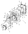
- the disassembled perspective view of the electronic control unit which concerns on this embodiment.
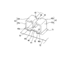
- the perspective view of the 2nd electricity supply terminal. The block diagram of a power steering apparatus.
- the perspective view of the modification of the 2nd electricity supply terminal is
- An electronic control device includes two casing members that are located in opposite directions and can be joined to each other, and a circuit board is provided and accommodated in one of the casing members.
- a first terminal (corresponding to first energization terminals 25 and 3e described later) disposed on the other side of the casing member and a second terminal (corresponding to second energization terminals 35 and 37 described later) provided on the circuit board.
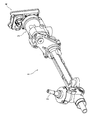
- the electric power steering apparatus 1 includes an input shaft 2 to which a steering torque is input from a steering wheel, and a motor unit 3 that applies assist torque to the steering torque. Is driven and controlled by an electronic control unit (ECU) 4, and the electronic control device of this embodiment can be applied to the electronic control unit 4.
- ECU electronice control unit
- the electronic control unit 4 shown in FIGS. 1 to 7 is, for example, as shown in FIGS. 8 on the side corresponding to 8).
- the motor unit 3 includes an electric motor (three-phase AC brushless motor) (not shown), a motor housing 3c that houses the electric motor, the shaft 3a that is rotationally driven by the electric motor, and a base end of the shaft 3a. And a magnet S for detecting rotation of the shaft 3a by a hall element 47, which will be described later, and a first energizing terminal (three-phase motor terminal) 3e connected to the three-phase terminals of the motor. .
- the shaft 3a is rotated by driving the electric motor, and applies assist torque to the steering torque via a reduction gear (not shown).
- an exterior portion 3f having a large outer dimension is formed on the electronic control unit 4 side of the motor housing 3c.
- the electronic control unit 4 includes a case (housing member) 5 that is fixed to the exterior portion 3f of the motor housing 3c, a cover (housing member) 6 that is joined to the case 5, and a space between the five and six.
- a drive circuit board 7 that is housed in the drive circuit and drives the electric motor
- a control circuit board 8 that is housed between the two and 6 and controls the drive of the drive circuit board 7, and each circuit from a power supply battery (not shown). It has the board
- Case 5 The case 5 is a part of a housing that accommodates the circuit boards 8, 8.
- the case 5 is formed in a box shape with an upper portion made of an aluminum alloy material, for example, and is erected on the edge of the bottom plate 5 a and the bottom plate 5 b. As shown in FIG. 1, the upper portion of the bottom plate 5a is formed so as to protrude in the opposite direction to the side plate 5b.
- An opening 10 for attaching the electrical connector 9 is formed at the top of the bottom plate 5a, holes 10a are provided around the outer periphery of the opening 10, and female screws for fixing the electrical connector are provided at the upper four corners on the motor housing 3c side. 12 is formed.
- annular joint portion 11 is formed in the lower portion of the bottom plate 5a on the motor housing 3c side, and is fitted into the opening 3d of the exterior portion 3f, and female screw holes 17 for fixing to the exterior portion 3f are formed in the four corners.
- a shaft portion of a fixing screw (not shown) inserted into the through hole of the exterior portion 3f is fastened to the female screw hole 17.
- a circular opening 13 for receiving the sensor magnet S attached to the base end (shaft base end) of the shaft 3 a is formed in the center of the joint 11, and a three-phase motor side is formed below the opening 13.
- Three horizontally-long rectangular openings 14 through which the first energization terminals (three-phase motor terminals) 3e are inserted are formed, and energization connecting the two circuit boards 7 and 8 is performed obliquely above and to the left and right of the opening 13.
- a pair of vertically long rectangular openings 16 are formed at the tip of the terminal 15.
- a plurality of columnar substrate fixing portions 18 for fixing the control circuit substrate 8 are erected on the cover 6 side of the bottom plate 5a.
- a fitting groove 20 is provided around the upper end of each side plate 5b along the outer shape of the case 5, and a boss portion 19 is formed at a predetermined position on the outer surface of each side plate 5b.
- the cover 6 is formed of an aluminum alloy material or the like in a rectangular shape along the outer shape of the case 5, and closes the opening of the case 5.
- a fitting projection 23 that fits into the fitting groove 20 is provided around the edge of the cover 6 on the case 5 side along the outer shape.
- the cover 6 is formed with a group of female screws 21a for fixing the drive circuit board 7 to the left and right edges, and a boss portion 22 is formed on each end surface at a position corresponding to the boss portion 19. Omitted through holes are formed. A shaft portion of a fixing screw (not shown) inserted through the through hole is fastened to a female screw hole of the boss portion 19. A heat sink (not shown) is formed on the side of the cover 6 opposite to the case 5.
- the electrical connector 9 is attached to the outer peripheral edge of the opening 10 of the case 5, and as shown in FIGS. 1 to 3 and 5, the substantially central portion of the first conductive terminal (power supply terminal) 25 on the connector side is sealed with resin.
- the second connector 28 includes a connector holder for holding the first connectors C1 to C3, and three attachment holes 29a through which the first connectors C1 to C3 are inserted are formed.
- the outer peripheries of the resin portions 30 of the first connectors C1 to C3 are coupled to the inner surfaces of the mounting holes 29a, and the first connectors C1 to C3 are held and fixed to the second connector 28.
- the first connectors C1 to C3 in which the substantially central portions of the terminals 25 to 27 are sealed with resin are inserted into the mounting holes 29a of the second connector 28, respectively.
- an adhesive (sealing material) is applied to the gap between the two C1 to C3 and 28 to reinforce the waterproofness of the gap and the bonding force between the two C1 to C3 and 28.
- the electrical connector 9 is completed by coupling the two connectors C1 to C3 and 28, and is attached to the outer peripheral edge of the opening 10.
- the mounting portion 28a to be mounted in the circumferential groove 10b formed on the outer peripheral edge of the opening 10 is provided on the case 5 side of the second connector 28, while the connector is fitted on the opposite side to the case 5.
- Joint portions 33a to 33c are formed.
- through holes 30a are formed at the four corners of the second connector 28, and shaft portions of fixing screws (not shown) inserted into the through holes 30a are fastened to the female screw holes 12 of the case 5, and the through holes at both ends are provided.
- the pin 31 inserted in the hole 10a of case 5 is formed. Since the pins 31 and the holes 10a are formed in an asymmetrical number, it is possible to prevent the electrical connector 9 from being attached to the left and right by mistake.
- each of the terminals 25 to 27 (one end of the terminal 25 corresponds to, for example, one end 90 in FIG. 9; hereinafter, reference numerals and the like are omitted as appropriate) is arranged on the drive circuit board 7 side, while the other end Are arranged in the connector fitting portions 33a to 33c.
- one end of each of the terminals 26 and 27 is formed in a pin shape, while one end of the first energizing terminal 25 is formed in a tapered band shape, and the tip thereof Are cut into a V shape, and the inner surfaces of the tip ends of the pair of sandwiching portions 25a are formed in a tapered shape.
- One end of the three-phase-side first energization terminal 3e (one end of the terminal 3e corresponds to, for example, one end 90 of FIG. 9; hereinafter, reference numerals and the like are omitted as appropriate) also has a similar tapered shape. To do. ).
- Each connector fitting portion 33a to 33c is fitted with a connector fitting portion formed on an electrical connector of an external device (not shown) such as a power supply battery, and the other end portions of the terminals 25 to 27 are externally connected. Electrically connected to the terminal of the electrical connector of the device.
- the drive circuit board 7 converts the current supplied from the electrical connector 9 into three-phase (U-phase, V-phase, W-phase) alternating current, and drives the electric motor in accordance with a control signal from the control circuit board 8. Regarding modules.
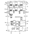
- a wiring pattern (not shown) is formed on a plate made of a metal material serving as a base via an insulating layer. As shown in FIG. 4A, one end of each first energization terminal 25 is formed. And a driving transistor (driving element, switching element) 36 in which the upstream side P and the downstream side Q are electrically connected in series for each phase of the three-phase alternating current. And the 2nd electricity supply terminal 37 for three-phase motors electrically connected with the one end part of each said 1st electricity supply terminal 3e is mounted.
- the drive transistor 36 is mounted on the drive circuit board 7 in an array of “two (a set in which the upstream P and the downstream Q are a pair) ⁇ 3 sets (for three phases)”.
- the second energization terminal 37 is arranged between the drive transistor 36 and each of the downstream drive transistors 36, and supplies a three-phase alternating current to each first energization terminal 3e.
- Each said 2nd electricity supply terminal 35 is arrange
- the drive circuit board 7 is mounted with electronic components such as the smoothing capacitor 38 of FIG. 4, the fail-safe relay 39 when a failure occurs, and the coil 60.
- the smoothing capacitor 38 smoothes the current supplied by the connection between the current-carrying terminals 25 and 35 and supplies the smoothed current to the driving transistors 35.
- the base end portion of the energizing terminal 15 is electrically joined to the left and right edge portions of the drive circuit board 7 and a group of through holes 45 for fixing to the cover 6 is formed.
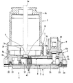
- the shaft portion of the fixing screw 46 inserted through each through hole 45 is fastened to the female screw hole 21 of the cover 6 as shown in FIG.
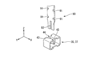
- Second energization terminals 35 and 37 Each of the second energization terminals 35 and 37 is formed by bending a metal plate material such as a copper material, and is electrically joined to a land portion 71 formed at a predetermined position of the drive circuit board 7, for example, as shown in FIG.
- bent portion proximity directions a pair of bent portions 42 that are erected from both ends 40a and 40b of the bottom surface portion 40 and bent in directions close to each other
- connection portions 43 a pair of connection portions 43 that are formed on the sides and are opposed to each other (opposing in the bent portion proximity direction)
- One end of the first energization terminal 3e is press-fitted and can be electrically connected.
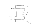
- the land portion 71 can be formed by opening a desired position according to the shape of the bottom surface portion 40 in a mask 72 formed by masking a photoresist or the like on one end surface side of the drive circuit board 7, for example. Since the land portion 71 and the bottom surface portion 40 are electrically joined to fix the second current-carrying terminals 35 and 37, the fixed support area (the land portion 71 and the bottom surface portion 40 is compared with the case where a tuning fork terminal or the like is used). And a stable connection structure can be obtained.
- Each bent portion 42 includes an upright portion 42a projecting in the thickness direction of the drive circuit board 7 from both ends 40a or 40b of the bottom surface portion 40 facing each other, and a bent portion approaching from the distal end side of each upright portion 42a.
- An extension portion 42b extending in the direction, and press-fitting of one end portion of the first energization terminal 25 and one end portion of the first energization terminal 3e into the gap portion 44 between the connection portions 43 (rise of the upright portion 42a) It is configured to be elastically deformed by press-fitting from the direction side).
- the distance between the connecting portions 43 (the width of the gap portion 44) is set to be smaller than the dimension in the cross-sectional direction of one end portion of the first energizing terminal 25 or one end portion of the first energizing terminal 3e, thereby allowing both terminals 25 , 3e is set to be press-fitted into the gap portion 44 with a predetermined pressure input (hereinafter referred to as terminal pressure input), that is, the distance between the connection portions 43 is expanded and the bending portions 42 are elastically deformed to press-fit. Can be set.
- terminal pressure input a predetermined pressure input
- each bent portion 42 elastically deformed as described above is Can be set to act as a force. Therefore, since each bending part 42 can also be designed so that clamping force may become a desired magnitude
- each connecting portion 43 in FIG. 6 is formed to bend and extend from the distal end side of each bent portion 42 (the distal end side of the extending portion 42b in FIG. 6) to the bottom surface portion 40 side.
- One end portion of the first energizing terminal 25 and one end portion of the first energizing terminal 3e are easily press-fitted into the gap portion 44 along the extending direction of the portion 43, and one end portion of each of the terminals 25 and 3e thus press-fitted Is configured to be easily held between the connection portions 43.
- Control circuit board 8 is configured by a printed board (glass epoxy board) or a ceramic board.
- the control circuit board 8 includes a microcomputer (CPU: hereinafter abbreviated as a microcomputer) 46 that controls each drive transistor 36 and a hall element that detects the rotation of the electric motor. Have.
- CPU central processing unit
- the microcomputer 46 is mounted on the surface of the control circuit board 8 facing the drive circuit board 7, while the hall element 47 is accommodated in the surface opposite to the microcomputer 46, that is, the opening 13 of the case 5.
- the both 46 and 47 are electrically connected through the circuit pattern of the control circuit board 8, and the circuit pattern is a signal transmission path between the both 46 and 47.
- the Hall element 47 is disposed at a position facing the sensor magnet S on one end side of the control circuit board 8, detects the magnetic field of the sensor magnet S using the Hall effect, and rotates the shaft 3a. Is detected. This detection signal is input to the microcomputer 46 through the circuit pattern of the control circuit board 8.
- the tip end portion of the energizing terminal 15 is inserted into one end side of the control circuit board 8 and is electrically connected by soldering or welding.
- a cutout portion 49 is formed on the other end portion side of the control circuit board 8 to allow one end portion of the energization terminal 25 to pass to the drive circuit board 7 side.
- One ends of the terminals 26 and 27 are inserted into and electrically connected to both sides of the notch 49.
- the microcomputer 46 controls the drive transistor 35 based on information (for example, steering torque, vehicle speed signal, etc.) inputted from the outside through the both terminals 26 and 27 of the electrical connector 9 and a detection signal of the Hall element 47.
- information for example, steering torque, vehicle speed signal, etc.
- through holes 48 are formed in the left and right edges of the control circuit board 8, and as shown in FIGS. 2 and 3, the shaft portion of the fixing screw 49 inserted into each through hole 48 is the board of the case 5. It is fastened to the female screw hole of the fixing portion 18.
- the shaft portion of the fixing screw 49 When mounting the control circuit board 8, the shaft portion of the fixing screw 49 is inserted into each through hole 48 of the control circuit board 8 with the Hall element 47 facing the opening 13 of the cover 6, and then each fixing is performed. The shaft portion of the screw 49 is fastened to the female screw hole of each substrate fixing portion 18 of the case 5.
- the first connectors C1 to C3 in which the substantially central portions of the terminals 25 to 27 are sealed with resin are inserted into the second connector 28 and the connection is completed. Attach to the periphery. That is, the mounting portion 28a of the connector holder 28 is fitted into the circumferential groove 10b of the case 5, and the pin 31 is fitted into the hole 10a. Thereafter, the shaft portion of the fixing screw is inserted into the through hole 30a and fastened to the female screw hole 12, and then one end portions of the terminals 26 and 27 are electrically joined to the control circuit board 8 by soldering. When attaching the drive circuit board 7, the shaft portion of the fixing screw 46 is inserted into the through hole 45 of the drive circuit board 7 and fastened to the screw hole 21 of the cover 6.
- the case 5 to which the electrical connector 9 and the control circuit board 8 are attached and the cover 6 to which the drive circuit board 7 is attached are assembled.
- one end of the first energizing terminal 25 on the connector side is made to face the second energizing terminal 35 for power supply mounted on the drive circuit board 7 through the notch 49 of the control circuit board 8.
- the fitting protrusion 23 of the cover 6 is fitted into the fitting groove 20 of the case 5, and both 20 and 23 are fitted.
- one end portion of the first energization terminal 25 is press-fitted into the gap portion 44 between the connection portions 43 of the second energization terminal 35 by the fitting force of the fitting protrusion 23 into the fitting groove 20. That is, one end portion of the first energizing terminal 25 is press-fitted into the gap portion 44 while elastically deforming each bent portion 42 of the second energizing terminal 35 when both 5 and 6 are assembled. It will be in the state clamped by each connection part 43 with the clamping force by the restoring action of the part 42.
- the fitting protrusion 23 of the cover 6 is inserted into the fitting groove 20 of the case 5, and at the same time, one end of the first energizing terminal 25 is inserted into the gap 44 between the connecting portions 43 of the second energizing terminal 35.
- the two energization terminals 25 and 35 are directly (electrically) connected by being press-fitted against each other and sandwiched and electrically joined by the connection portions 43.
- both energizing terminals 25 and 35 can be connected with sufficient connection reliability. Further, it is not necessary to apply a tuning fork terminal to both the energizing terminals 25 and 35, and this can contribute to downsizing of the apparatus.
- one end portion of the first energization terminal 25 is simply sandwiched and connected to each connection portion 43, that is, connected to be detachable, both the energization terminals 25 and 35 are electrically connected to each other and connected. Even if it exists, it can insert / extract easily, and it becomes easy to perform the electrical test
- the front ends of the energizing terminals 15 are inserted into the control circuit board 8, and the left and right openings of the case 5 are opened as shown in FIG. Since the housing 5 is accommodated and disposed, the energizing terminal 15 can be electrically connected to the control circuit board 8 by soldering or welding after the case 5 and the cover 6 are assembled. In this respect, the control circuit board 8 and the drive circuit board 7 can be arranged in a stacked state. After this electrical joining operation, the shaft portion of the fixing screw is inserted into the through hole of the boss portion 22 of the cover 6, and the shaft portion is fastened to the female screw hole of the boss portion 19 of the case 5. Assembly is completed.
- each first energization terminal 3e faces each opening 14 of the case 5, and therefore, each connection portion of the second energization terminal 37 is simultaneously inserted with the joint portion 14 like the second energization terminal 35. It press-fits into the gap portion 44 between 43, is sandwiched between the connection portions 43 and is electrically connected, and both energization terminals 3e and 37 are directly (electrically) connected.
- both the energization terminals 3e and 37 can be connected with sufficient connection reliability, contributing to downsizing of the apparatus, and electronic control. It becomes easy to perform the electrical inspection and the motor characteristic inspection of the unit 4 in the insertion / extraction state.
- the electronic control unit 4 is attached to the motor housing 3c by inserting the shaft portion of the fixing screw through the through hole of the boss portion 3g and fastening the shaft portion to the female screw hole 17 of the case 5.
- the electric motor and the power module are fixed to different housing members (case 5 or cover 6), the thermal interference generated in each can be suppressed, which can contribute to improvement of heat dissipation.
- the second current-carrying terminal 37 is disposed between the upstream-side P drive transistor 36 and the downstream-side Q drive transistor 36 in view of the component arrangement of the drive circuit board 7, the shaft 3 a of the electric motor and the second Arrangement interference with the two energizing terminals 37 can be suppressed. Furthermore, since the wiring distance between both drive transistors 36 and the second energization terminal 37 can be shortened, the complexity of the wiring can also be suppressed.
- the assembly order of the electronic control unit 4 is not particularly limited, and the motor unit 3 and the case 5 may be assembled first, and then the case 5 and the cover 6 may be assembled.
- the second energization terminals 35 and 37 stand up from the bottom surface portion 40 that is connected and fixed to the land portion 71 at a predetermined position of the circuit board 7 and from both ends of the bottom surface portion 40.
- Various terminals for example, a connection target
- the design can be changed as appropriate as long as the first energizing terminals 25 and 3e are configured to be press-fitted between the pair of connecting portions 43 from the standing direction side of the bent portion 42 and electrically connected. is there.
- the second energizing terminal 35, 37 can be automatically mounted on a predetermined position of the circuit board 7, which can contribute to simplification of the manufacturing man-hours of the apparatus and can reduce the work effort.
- the bottom surface portion 40 may be configured to be electrically joined and fixed to the land portion 71, and a conductive bonding material such as solder (not shown) between the bottom surface portion 40 and the land portion 71. It may be a structure that is electrically joined (soldered or the like) with a gap interposed, or a structure that is electrically joined by welding or the like. When various electronic components (such as a smoothing capacitor 38) mounted on the circuit board 7 are electrically joined by a conductive bonding material such as solder, the bottom surface portion 40, the land portion, Can be electrically joined (electrically joined by the same conductive binder), which can contribute to simplification of the manufacturing man-hours and reduce the work effort.
- solder solder
- the shape of the bottom surface portion 40 can be appropriately set according to the shape of the land portion 71 and the like. However, as the shape of the bottom surface portion 40 increases, that is, the fixed support area (land portion 71 for the land portion 71).
- the connection structure of the second energization terminals 35 and 37 with respect to the land portion 71 becomes more stable, for example, the connection area of the first energization terminals 25 and 3e between the connection portions 43 increases.
- the durability against press-fitting is also improved.
- motor efficiency due to a decrease in electrical resistance is improved, and generation of heat is suppressed.
- a through hole 45 penetrating in the thickness direction in the bottom surface portion 40 when electrically joined to the land portion 71 via a conductive binder, it has a relatively soft property such as liquid or semi-liquid.
- the conductive bonding material in a state is easily filled into the through-hole 45, and an anchor effect is obtained by solidifying the filled conductive bonding material (the filled conductive bonding material functions as an anchor), and the connection The structure becomes more stable.
- the land portion 71 may have a structure having a mask region 72a with a mask 72 interposed between both end portions 71a and 71b and the central portion 71c.
- a conductive bonding material for example, terminal pressure input acts on both end portions 40 a and 40 b of the bottom surface portion 40, and both end portions of the land portion 71.
- the mask region 72a prevents the crack from progressing to the conductive bonding material on the central portion 71c side, so that connection reliability is maintained. It can be said that it becomes easy to be done.
- a notch 71d may be formed in the central portion 71c of the land portion 71 to form a constricted shape.
- the bottom surface portion 40 may be formed in a constricted shape by forming the notch portion 41 in the central portion 40c in accordance with the shape of the land portion 71.
- a conductive binder interposed between the constricted land portion 71 and the bottom surface portion 40 when it is in a relatively soft state such as liquid or semi-liquid and protrudes from between the two 40, 71, The protruding conductive binder is likely to return between the portions 40 and 71 due to surface tension acting at the positions of the notches 41 and 71d.
- One end portions of the first energization terminals 25 and 3e are elastically deformed in the Y direction in the drawing by forming a groove portion 91 on the side edge side of the one end portion 90, for example, as one end portion 90 shown in FIG. It may be easy. Thereby, even when the press-fit angle when the press-fit angle is inserted into the gap 44 between the connection portions 43 of the terminals 35 and 37 is displaced, the one end portion 90 is easily corrected in the Y direction in the figure, and the connection reliability is improved. It becomes easy to obtain.
- the groove portion 92 is formed on the distal end side of the one end portion 90, the one end portion 90 is easily elastically deformed with respect to the X direction or the ⁇ direction in the drawing, and even if the press-fit angle is misaligned. Is easily corrected in the X direction and ⁇ direction in the figure, and connection reliability is easily obtained.
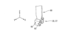
- a groove 93 may be formed on the side edge side of the bent portion 42, and the bent portion 42 is easily elastically deformed. It can contribute to reliability.
- the first energizing terminals 25 and 3e and the second energizing terminals 35 and 37 can be made of various materials as long as they can be electrically connected to each other.
- the first energizing terminals 25 and 3e are made of a conductive material such as pure copper
- the second energizing terminals 35 and 37 are made of a conductive material such as phosphor bronze and are elastic. It is mentioned to apply what has.
- the present invention is not limited to the configuration of the embodiment and the like, and can be modified and implemented within the scope described in each claim.
- the present invention can be applied not only to the electric power steering device 1 but also to an electronic control device (electronic control unit) such as an electric brake device of an automobile or a variable valve device of an internal combustion engine.
- the first energizing terminal 3 e can be coupled to the motor side terminal by joining the case 5 and the cover 6.
- the first connectors C1 to C3 in which the substantially central portions of the terminals 25 to 27 are sealed with resin, are inserted into the mounting holes 29a of the second connector 28 and coupled.
- an adhesive is applied to the gap between the two C1 to C3 and 28 to enhance the waterproofness of the gap and the bonding force between the two C1 to C3 and 28.
- the electrical connector 9 is attached to the outer peripheral edge of the opening 10 of the case 5, and one end of the first energization terminal 3 e is coupled to the second energization terminal 37 of the drive circuit board 7. If the case 5 and the cover 6 are assembled in this state, one end of the first energizing terminal 25 is coupled to the second energizing terminal 35 and at the same time, the other end of the first energizing terminal 3e is connected to the motor side in the motor housing 3c. Connect with terminal.
Landscapes
- Engineering & Computer Science (AREA)
- Microelectronics & Electronic Packaging (AREA)
- Chemical & Material Sciences (AREA)
- Combustion & Propulsion (AREA)
- Transportation (AREA)
- Mechanical Engineering (AREA)
- Manufacturing & Machinery (AREA)
- Power Steering Mechanism (AREA)
- Coupling Device And Connection With Printed Circuit (AREA)
- Motor Or Generator Frames (AREA)
- Electric Connection Of Electric Components To Printed Circuits (AREA)
Abstract
Description
図1~図7の電子制御ユニット4は、例えば図1~図3に示すように、モータユニット3のシャフト3aの基端部側(出力側の端部と反対側、即ち後述する制御回路基板8と対応する側の端部)に配置されている。
ケース5は、回路基板8,8を収容する筐体の一部であり、例えばアルミニウム合金材などで上部が開口したボックス状に形成され、底板5aと該底板5bの縁部に立設された側板5bとを有し、図1に示すように、底板5aの上部が側板5bと反対方向に突出形成されている。
カバー6は、例えば図1~3に示すように、アルミニウム合金材などをケース5の外形に沿った長方形状に形成され、ケース5の開口部を閉塞する。このカバー6のケース5側の縁部には嵌合溝20に嵌入する嵌合突部23が外形に沿って周設されている。
電気コネクタ9は、ケース5の開口部10の外周縁に取り付けられ、図1~図3および図5に示すように、コネクタ側の第1通電端子(電源端子)25の略中央部を樹脂封入した一対の第1コネクタC1と、各種信号端子(トルク/S、イグニッションSW等)26の略中央部を樹脂封入した第1コネクタC2と、CAN通信用端子27の略中央部を樹脂封入した第1コネクタC3と、第1コネクタC1~C3が固定される第2コネクタ28と、を有し、開口部10は第2コネクタ28により閉塞されている。
駆動回路基板7は、電気コネクタ9から供給される電流を三相(U相,V相,W相)交流に変換し、制御回路基板8からの制御信号に応じて前記電動モータを駆動させるパワーモジュールに関する。
各第2通電端子35,37は、銅材などの金属板材を折曲して形成され、例えば図6に示すように、駆動回路基板7の所定位置に形成されたランド部71に電気接合して固定される底面部40と、底面部40の両端40a,40b側から起立して互いに近接する方向(以下、屈曲部近接方向)に屈曲した一対の屈曲部42と、各屈曲部42の先端側に形成され互いに対向(屈曲部近接方向において対向)して位置する一対の接続部43と、を有し、各接続部43間の隙間部44に対し、第1通電端子25の一端部や第1通電端子3eの一端部を圧入して電気的に接続できるように構成される。
制御回路基板8は、プリント基板(ガラスエポキシ基板)またはセラミック基板により構成されている。この制御回路基板8は、例えば図1に示すように、各駆動トランジスタ36を制御するマイクロコンピュータ(CPU:以下、マイコンと省略する。)46と、前記電動モータの回転を検出するホール素子とを有している。
以下、電子制御ユニット4の組立手順を説明する。まずケース5に制御回路基板8および電気コネクタ9を取り付けるとともに、カバー6に駆動回路基板7を取り付けておく。
例えば第2通電端子35,37は、図6等に基づいて前述したように、回路基板7の所定位置のランド部71に接続固定される底面部40と、底面部40の両端側から起立し互いに屈曲部近接方向に屈曲した一対の屈曲部42と、各屈曲部42の先端側に形成され互いに対向して位置する一対の接続部43と、を有し、接続対象である各種端子(例えば第1通電端子25,3eの一端部)を屈曲部42の起立方向側から前記の一対の接続部43間に圧入して電気的に接続できる構成であれば、適宜設計変更することが可能である。
本発明は、前記実施形態の構成などに限定されるものではなく、各請求項に記載した範囲内で変形して実施することができる。例えば本発明は電動パワーステアリング装置1に限らず、自動車の電動ブレーキ装置や内燃機関の可変動弁装置などの電子制御装置(電子制御ユニット)にも適用することができる。
[請求項a] 請求項1~3の何れかに記載の電子制御装置において、
ランド部の中央部は、当該中央部に切欠部を形成して括れ状にした電子制御装置
[請求項b] 請求項1~3の何れかに記載の電子制御装置において、
底面部は、当該底面部の肉厚方向に貫通した貫通孔が形成された電子制御装置。
Claims (3)
- 互いに対向方向に位置して接合可能な二つの筐体部材を備えた筐体内に、電子部品を実装した回路基板が収容され、その回路基板が前記筐体部材のうち一方に設けられた電子制御装置であって、
前記筐体部材のうち他方側に配置される第1端子と、回路基板に設けられる第2端子と、が前記の二つの筐体部材の接合によって接続され、
前記第2端子は、回路基板のランド部に電気接合して固定される底面部と、底面部の両端側から起立して互いに近接する方向に屈曲した一対の屈曲部と、前記の各屈曲部の先端側に形成され互いに対向して位置する一対の接続部と、を有し、
前記の一対の接続部間に、第1端子の先端側が前記屈曲部の起立方向側から圧入して接続された電子制御装置。 - 前記ランド部は、当該ランド部における両端部と中央部との間にマスク領域が形成され、ランド部におけるマスク領域以外と底面部とに導電性結合材を介在させて、当該ランド部と底面部とを電気接合した請求項1記載の電子制御装置。
- 前記各屈曲部は、底面部における互いに対向して位置する両端側から起立した一対の起立部と、各起立部の先端側から前記屈曲部の近接方向に延出した延出部と、を有した請求項1または2記載の電子制御装置。
Priority Applications (8)
| Application Number | Priority Date | Filing Date | Title |
|---|---|---|---|
| US14/913,784 US9701335B2 (en) | 2013-09-19 | 2014-08-20 | Electronic control device |
| CN201480037922.8A CN105359345B (zh) | 2013-09-19 | 2014-08-20 | 电子控制装置 |
| KR1020187031120A KR101968067B1 (ko) | 2013-09-19 | 2014-08-20 | 전자 제어 장치 |
| DE112014004327.3T DE112014004327B4 (de) | 2013-09-19 | 2014-08-20 | Elektronische Steuerungsvorrichtung |
| KR1020167000792A KR101918824B1 (ko) | 2013-09-19 | 2014-08-20 | 전자 제어 장치 |
| US15/616,097 US10435060B2 (en) | 2013-09-19 | 2017-06-07 | Electronic control device |
| US15/616,243 US10065672B2 (en) | 2013-09-19 | 2017-06-07 | Electronic control device |
| US16/576,493 US11312408B2 (en) | 2013-09-19 | 2019-09-19 | Electronic control device |
Applications Claiming Priority (2)
| Application Number | Priority Date | Filing Date | Title |
|---|---|---|---|
| JP2013194530A JP6117661B2 (ja) | 2013-09-19 | 2013-09-19 | 電子制御装置 |
| JP2013-194530 | 2013-09-19 |
Related Child Applications (3)
| Application Number | Title | Priority Date | Filing Date |
|---|---|---|---|
| US14/913,784 A-371-Of-International US9701335B2 (en) | 2013-09-19 | 2014-08-20 | Electronic control device |
| US15/616,097 Continuation US10435060B2 (en) | 2013-09-19 | 2017-06-07 | Electronic control device |
| US15/616,243 Continuation US10065672B2 (en) | 2013-09-19 | 2017-06-07 | Electronic control device |
Publications (1)
| Publication Number | Publication Date |
|---|---|
| WO2015040994A1 true WO2015040994A1 (ja) | 2015-03-26 |
Family
ID=52688650
Family Applications (1)
| Application Number | Title | Priority Date | Filing Date |
|---|---|---|---|
| PCT/JP2014/071700 Ceased WO2015040994A1 (ja) | 2013-09-19 | 2014-08-20 | 電子制御装置 |
Country Status (6)
| Country | Link |
|---|---|
| US (4) | US9701335B2 (ja) |
| JP (1) | JP6117661B2 (ja) |
| KR (2) | KR101918824B1 (ja) |
| CN (1) | CN105359345B (ja) |
| DE (1) | DE112014004327B4 (ja) |
| WO (1) | WO2015040994A1 (ja) |
Cited By (2)
| Publication number | Priority date | Publication date | Assignee | Title |
|---|---|---|---|---|
| CN106208622A (zh) * | 2015-05-26 | 2016-12-07 | 株式会社电装 | 合并到壳体中的功率转换器 |
| JP2020198768A (ja) * | 2019-06-05 | 2020-12-10 | 株式会社デンソー | 電力変換機 |
Families Citing this family (25)
| Publication number | Priority date | Publication date | Assignee | Title |
|---|---|---|---|---|
| WO2015087555A1 (ja) * | 2013-12-13 | 2015-06-18 | 日本精工株式会社 | 電子制御ユニット、電動パワーステアリング装置及び車両 |
| JP6248984B2 (ja) | 2014-07-31 | 2017-12-20 | 株式会社デンソー | 駆動装置 |
| JP5972508B1 (ja) * | 2015-02-23 | 2016-08-17 | 三菱電機株式会社 | 半導体電力変換器 |
| CN108028611B (zh) * | 2015-09-11 | 2020-04-21 | 日立汽车系统株式会社 | 电路装置 |
| JP6576268B2 (ja) * | 2016-03-02 | 2019-09-18 | 日立オートモティブシステムズ株式会社 | 電動駆動装置 |
| JP6992754B2 (ja) * | 2016-08-05 | 2022-01-13 | 日本電産株式会社 | モータ |
| GB201710104D0 (en) * | 2017-06-23 | 2017-08-09 | Trw Ltd | Electric power assisted steering |
| JP6400795B1 (ja) * | 2017-06-29 | 2018-10-03 | タイコエレクトロニクスジャパン合同会社 | 印刷回路基板 |
| JP2019067896A (ja) * | 2017-09-29 | 2019-04-25 | 日本電産エレシス株式会社 | 回路基板、および制御装置 |
| CN207304475U (zh) * | 2017-10-25 | 2018-05-01 | 江苏英迈能源科技有限公司 | 功能整合型可拆卸式光伏组件接线盒 |
| JP2019080471A (ja) | 2017-10-27 | 2019-05-23 | オムロンオートモーティブエレクトロニクス株式会社 | 負荷駆動装置 |
| US11239723B2 (en) | 2017-10-31 | 2022-02-01 | Deere & Company | Interconnection device |
| JP7085439B2 (ja) * | 2018-08-10 | 2022-06-16 | 日立Astemo株式会社 | 電動駆動装置、及び電動パワーステアリング装置 |
| US11767053B2 (en) | 2018-12-27 | 2023-09-26 | Hitachi Astemo, Ltd. | Electronic control device and electric power steering device |
| US10932378B2 (en) * | 2018-12-30 | 2021-02-23 | Vitesco Technologies USA, LLC | Connector having pins extending to more than one printed circuit board |
| TWI741311B (zh) * | 2019-06-21 | 2021-10-01 | 飛宏科技股份有限公司 | 具防水結構的連接器與製造方法 |
| US11594832B2 (en) * | 2020-02-13 | 2023-02-28 | Super Micro Computer, Inc. | Electronic devices for expansion |
| US11211721B2 (en) * | 2020-03-19 | 2021-12-28 | Lear Corporation | Threaded stud within a conductive bushing connecting a printed circuit board |
| DE102021107894B4 (de) * | 2020-03-30 | 2026-02-05 | Steering Solutions Ip Holding Corporation | Leistungsinduktivität mit nachgiebigen stiften und batterie-schnittstelle |
| JP7610980B2 (ja) * | 2020-12-25 | 2025-01-09 | ニデックインスツルメンツ株式会社 | 制御装置 |
| JP2022123714A (ja) * | 2021-02-12 | 2022-08-24 | 京セラ株式会社 | コネクタ及び電子機器 |
| CN115123372B (zh) | 2021-03-25 | 2024-07-09 | 操纵技术Ip控股公司 | 用于电动助力转向系统的动力机组 |
| DE102022206942B3 (de) | 2022-07-07 | 2023-08-03 | Zf Friedrichshafen Ag | Kontaktvorrichtung, Leiterplattenvorrichtung, Verfahren zum Herstellen einer Leiterplattenvorrichtung, Stromrichter, elektrischer Antrieb sowie Kraftfahrzeug |
| US12453018B2 (en) * | 2022-11-30 | 2025-10-21 | Rosemount Inc. | Vibration damped electronics assemblies for process variable transmitters |
| CN117997319B (zh) * | 2024-04-03 | 2024-06-04 | 江苏固特电气控制技术有限公司 | 一种耐高温的固态继电器 |
Citations (6)
| Publication number | Priority date | Publication date | Assignee | Title |
|---|---|---|---|---|
| JPS5143887U (ja) * | 1974-09-30 | 1976-03-31 | ||
| JPH01130271U (ja) * | 1988-02-29 | 1989-09-05 | ||
| JP2000307056A (ja) * | 1999-04-22 | 2000-11-02 | Mitsubishi Electric Corp | 車載用半導体装置 |
| JP2001326477A (ja) * | 2000-05-17 | 2001-11-22 | Matsushita Electric Ind Co Ltd | 電子機器 |
| JP2004357129A (ja) * | 2003-05-30 | 2004-12-16 | Nippon Soken Inc | メータ装置 |
| JP2006066123A (ja) * | 2004-08-25 | 2006-03-09 | Fujikura Ltd | 電気接続箱の接続端子構造 |
Family Cites Families (44)
| Publication number | Priority date | Publication date | Assignee | Title |
|---|---|---|---|---|
| US4157582A (en) * | 1978-02-21 | 1979-06-05 | Gould Inc. | Plug-in contact structure for panelboard |
| US4326765A (en) * | 1980-04-15 | 1982-04-27 | International Telephone And Telegraph Corporation | Electronic device carrier |
| US4449165A (en) * | 1982-03-01 | 1984-05-15 | Kaufman Lance R | Compact circuit package having an improved lead frame connector |
| US4629278A (en) * | 1985-04-15 | 1986-12-16 | Amp Incorporated | Surface mountable connector retention means and method |
| DE4034423C2 (de) | 1989-10-30 | 1998-10-08 | Amp Inc | Schaltungsplattenkontakt |
| JP2642548B2 (ja) * | 1991-09-26 | 1997-08-20 | 株式会社東芝 | 半導体装置およびその製造方法 |
| JP3429862B2 (ja) | 1994-06-30 | 2003-07-28 | カヤバ工業株式会社 | 電動パワーステアリング装置 |
| JP3996668B2 (ja) * | 1997-05-27 | 2007-10-24 | 富士通株式会社 | 半導体装置用ソケット |
| US5986880A (en) * | 1997-06-16 | 1999-11-16 | Compaq Computer Corporation | Electronic apparatus having I/O board with cable-free redundant adapter cards thereon |
| WO1999016654A1 (fr) * | 1997-10-01 | 1999-04-08 | Kayaba Kogyo Kabushiki Kaisha | Moteur electrique pour dispositif de direction assistee |
| CN1139989C (zh) * | 1997-10-20 | 2004-02-25 | 株式会社日立制作所 | 半导体模块及使用该半导体模块的电力变换装置 |
| EP0926939B1 (en) * | 1997-12-24 | 2003-03-26 | Denso Corporation | Electronic circuit apparatus and method for assembling the same |
| JP3068557B2 (ja) * | 1998-04-30 | 2000-07-24 | 北川工業株式会社 | プリント配線板の接地構造及び当該接地構造に用いられる導電部材 |
| JP3417546B2 (ja) * | 1998-08-10 | 2003-06-16 | 矢崎総業株式会社 | 電気接続箱 |
| JP3644835B2 (ja) | 1999-01-18 | 2005-05-11 | 三菱電機株式会社 | 電動式パワーステアリング回路装置 |
| US6971170B2 (en) | 2000-03-28 | 2005-12-06 | Microjet Technology Co., Ltd | Method of manufacturing printhead |
| JP3774624B2 (ja) * | 2000-10-18 | 2006-05-17 | 三菱電機株式会社 | 電動パワーステアリング装置 |
| US6756711B2 (en) * | 2000-12-27 | 2004-06-29 | Asmo Co., Ltd. | Motor having control circuit board for controlling its rotation |
| DE10102671C2 (de) * | 2001-01-17 | 2003-12-24 | Eichenauer Heizelemente Gmbh | Elektrische Heizung für ein Kraftfahrzeug |
| US6642460B2 (en) * | 2002-01-23 | 2003-11-04 | Eaton Corporation | Switch assembly employing an external customizing printed circuit board |
| JP3638269B2 (ja) * | 2002-03-14 | 2005-04-13 | 三菱電機株式会社 | 電動式パワーステアリング装置 |
| US7040934B2 (en) * | 2002-12-19 | 2006-05-09 | Intel Corporation | Add-in card to backplane connecting apparatus |
| JP3692119B2 (ja) | 2003-02-18 | 2005-09-07 | 三菱電機株式会社 | 電動パワーステアリング装置並びにその製造法 |
| US7097495B2 (en) * | 2003-07-14 | 2006-08-29 | Tribotek, Inc. | System and methods for connecting electrical components |
| US7537461B2 (en) * | 2003-07-16 | 2009-05-26 | Gryphics, Inc. | Fine pitch electrical interconnect assembly |
| JP4161074B2 (ja) * | 2004-02-02 | 2008-10-08 | 三菱電機株式会社 | 電動式パワーステアリング装置 |
| JP4391407B2 (ja) * | 2004-12-20 | 2009-12-24 | 三菱電機株式会社 | 制御装置一体型回転電機 |
| JP4357514B2 (ja) | 2006-09-29 | 2009-11-04 | 株式会社東芝 | 液浸露光方法 |
| EP2623394B1 (en) | 2008-07-16 | 2014-08-20 | Mitsubishi Electric Corporation | Electric power steering apparatus and control device integrated type electric motor |
| JP4909961B2 (ja) * | 2008-09-02 | 2012-04-04 | 日立オートモティブシステムズ株式会社 | 電動パワーステアリング用制御装置 |
| JP5216558B2 (ja) | 2008-12-04 | 2013-06-19 | 日立オートモティブシステムズ株式会社 | ブレーキ用の制御装置 |
| JP5435284B2 (ja) * | 2009-06-24 | 2014-03-05 | 株式会社デンソー | 駆動装置 |
| JP5287787B2 (ja) * | 2010-04-16 | 2013-09-11 | 株式会社デンソー | 電動装置 |
| JP5012953B2 (ja) * | 2010-05-21 | 2012-08-29 | 株式会社デンソー | 駆動装置 |
| JP2012124294A (ja) | 2010-12-08 | 2012-06-28 | Sumitomo Electric Ind Ltd | 半導体モジュール及びその製造方法 |
| JP5599328B2 (ja) | 2011-01-20 | 2014-10-01 | 三菱電機株式会社 | 電力用半導体装置とプリント配線板との接続機構 |
| US8378211B2 (en) * | 2011-01-24 | 2013-02-19 | Sumitomo Wiring Systems, Ltd. | Electric connection box |
| JP5343989B2 (ja) | 2011-02-24 | 2013-11-13 | 株式会社デンソー | 電子制御装置 |
| JP5692593B2 (ja) * | 2011-05-11 | 2015-04-01 | 株式会社デンソー | 駆動装置 |
| WO2013038572A1 (ja) * | 2011-09-12 | 2013-03-21 | 三菱電機株式会社 | 電動式駆動装置 |
| US20130062137A1 (en) | 2011-09-14 | 2013-03-14 | Hitachi Automotive Systems, Ltd. | Electric Power Steering System |
| JP5741338B2 (ja) * | 2011-09-15 | 2015-07-01 | オムロン株式会社 | 端子部材のシール構造、及び、電磁継電器 |
| JP5827157B2 (ja) * | 2012-03-21 | 2015-12-02 | 日立オートモティブシステムズ株式会社 | 電動アクチュエータの端子接続構造 |
| JP2014061821A (ja) * | 2012-09-21 | 2014-04-10 | Hitachi Automotive Systems Ltd | 電子制御装置 |
-
2013
- 2013-09-19 JP JP2013194530A patent/JP6117661B2/ja active Active
-
2014
- 2014-08-20 CN CN201480037922.8A patent/CN105359345B/zh active Active
- 2014-08-20 DE DE112014004327.3T patent/DE112014004327B4/de active Active
- 2014-08-20 KR KR1020167000792A patent/KR101918824B1/ko not_active Expired - Fee Related
- 2014-08-20 US US14/913,784 patent/US9701335B2/en active Active
- 2014-08-20 WO PCT/JP2014/071700 patent/WO2015040994A1/ja not_active Ceased
- 2014-08-20 KR KR1020187031120A patent/KR101968067B1/ko not_active Expired - Fee Related
-
2017
- 2017-06-07 US US15/616,243 patent/US10065672B2/en active Active
- 2017-06-07 US US15/616,097 patent/US10435060B2/en active Active
-
2019
- 2019-09-19 US US16/576,493 patent/US11312408B2/en active Active
Patent Citations (6)
| Publication number | Priority date | Publication date | Assignee | Title |
|---|---|---|---|---|
| JPS5143887U (ja) * | 1974-09-30 | 1976-03-31 | ||
| JPH01130271U (ja) * | 1988-02-29 | 1989-09-05 | ||
| JP2000307056A (ja) * | 1999-04-22 | 2000-11-02 | Mitsubishi Electric Corp | 車載用半導体装置 |
| JP2001326477A (ja) * | 2000-05-17 | 2001-11-22 | Matsushita Electric Ind Co Ltd | 電子機器 |
| JP2004357129A (ja) * | 2003-05-30 | 2004-12-16 | Nippon Soken Inc | メータ装置 |
| JP2006066123A (ja) * | 2004-08-25 | 2006-03-09 | Fujikura Ltd | 電気接続箱の接続端子構造 |
Cited By (5)
| Publication number | Priority date | Publication date | Assignee | Title |
|---|---|---|---|---|
| CN106208622A (zh) * | 2015-05-26 | 2016-12-07 | 株式会社电装 | 合并到壳体中的功率转换器 |
| JP2016220500A (ja) * | 2015-05-26 | 2016-12-22 | 株式会社デンソー | 電力変換装置 |
| CN106208622B (zh) * | 2015-05-26 | 2020-04-14 | 株式会社电装 | 合并到壳体中的功率转换器 |
| JP2020198768A (ja) * | 2019-06-05 | 2020-12-10 | 株式会社デンソー | 電力変換機 |
| JP7120161B2 (ja) | 2019-06-05 | 2022-08-17 | 株式会社デンソー | 電力変換機 |
Also Published As
| Publication number | Publication date |
|---|---|
| CN105359345A (zh) | 2016-02-24 |
| CN105359345B (zh) | 2018-04-06 |
| KR20180120789A (ko) | 2018-11-06 |
| KR101968067B1 (ko) | 2019-04-10 |
| DE112014004327B4 (de) | 2023-12-21 |
| DE112014004327T5 (de) | 2016-06-02 |
| US20170282967A1 (en) | 2017-10-05 |
| JP6117661B2 (ja) | 2017-04-19 |
| US9701335B2 (en) | 2017-07-11 |
| US20170274927A1 (en) | 2017-09-28 |
| KR101918824B1 (ko) | 2018-11-14 |
| US11312408B2 (en) | 2022-04-26 |
| US10435060B2 (en) | 2019-10-08 |
| KR20160057377A (ko) | 2016-05-23 |
| US20160244088A1 (en) | 2016-08-25 |
| US20200010110A1 (en) | 2020-01-09 |
| US10065672B2 (en) | 2018-09-04 |
| JP2015060756A (ja) | 2015-03-30 |
Similar Documents
| Publication | Publication Date | Title |
|---|---|---|
| JP6117661B2 (ja) | 電子制御装置 | |
| JP6117577B2 (ja) | 電子制御装置 | |
| US9780016B2 (en) | Lead frame, electronic control device using lead frame, and lead-frame mounting method | |
| CN107041165B (zh) | 控制单元及使用了该控制单元的电动助力转向装置 | |
| JP6576268B2 (ja) | 電動駆動装置 | |
| JP2014151850A (ja) | 電子制御装置 | |
| CN106458249A (zh) | 一体型电动助力转向装置及其制造方法 | |
| JP6295354B2 (ja) | 電子制御装置 | |
| JP6445066B2 (ja) | 電子制御装置 | |
| JP6099915B2 (ja) | 電子制御装置 | |
| JP6445068B2 (ja) | 電子制御装置 | |
| JP2019160739A (ja) | 車両搭載機器のコネクタ構造 | |
| JP6499735B2 (ja) | 電子制御装置 |
Legal Events
| Date | Code | Title | Description |
|---|---|---|---|
| WWE | Wipo information: entry into national phase |
Ref document number: 201480037922.8 Country of ref document: CN |
|
| 121 | Ep: the epo has been informed by wipo that ep was designated in this application |
Ref document number: 14845598 Country of ref document: EP Kind code of ref document: A1 |
|
| ENP | Entry into the national phase |
Ref document number: 20167000792 Country of ref document: KR Kind code of ref document: A |
|
| WWE | Wipo information: entry into national phase |
Ref document number: 14913784 Country of ref document: US |
|
| WWE | Wipo information: entry into national phase |
Ref document number: 1120140043273 Country of ref document: DE Ref document number: 112014004327 Country of ref document: DE |
|
| 122 | Ep: pct application non-entry in european phase |
Ref document number: 14845598 Country of ref document: EP Kind code of ref document: A1 |