WO2015033736A1 - 多層基板 - Google Patents
多層基板 Download PDFInfo
- Publication number
- WO2015033736A1 WO2015033736A1 PCT/JP2014/070901 JP2014070901W WO2015033736A1 WO 2015033736 A1 WO2015033736 A1 WO 2015033736A1 JP 2014070901 W JP2014070901 W JP 2014070901W WO 2015033736 A1 WO2015033736 A1 WO 2015033736A1
- Authority
- WO
- WIPO (PCT)
- Prior art keywords
- multilayer substrate
- layer
- flexible
- reinforcing layer
- flexible portion
- Prior art date
- Legal status (The legal status is an assumption and is not a legal conclusion. Google has not performed a legal analysis and makes no representation as to the accuracy of the status listed.)
- Ceased
Links
Images




Classifications
-
- H—ELECTRICITY
- H05—ELECTRIC TECHNIQUES NOT OTHERWISE PROVIDED FOR
- H05K—PRINTED CIRCUITS; CASINGS OR CONSTRUCTIONAL DETAILS OF ELECTRIC APPARATUS; MANUFACTURE OF ASSEMBLAGES OF ELECTRICAL COMPONENTS
- H05K1/00—Printed circuits
- H05K1/02—Details
- H05K1/0277—Bendability or stretchability details
- H05K1/0283—Stretchable printed circuits
-
- H—ELECTRICITY
- H05—ELECTRIC TECHNIQUES NOT OTHERWISE PROVIDED FOR
- H05K—PRINTED CIRCUITS; CASINGS OR CONSTRUCTIONAL DETAILS OF ELECTRIC APPARATUS; MANUFACTURE OF ASSEMBLAGES OF ELECTRICAL COMPONENTS
- H05K1/00—Printed circuits
- H05K1/02—Details
- H05K1/0277—Bendability or stretchability details
- H05K1/028—Bending or folding regions of flexible printed circuits
-
- H—ELECTRICITY
- H05—ELECTRIC TECHNIQUES NOT OTHERWISE PROVIDED FOR
- H05K—PRINTED CIRCUITS; CASINGS OR CONSTRUCTIONAL DETAILS OF ELECTRIC APPARATUS; MANUFACTURE OF ASSEMBLAGES OF ELECTRICAL COMPONENTS
- H05K1/00—Printed circuits
- H05K1/02—Details
- H05K1/0277—Bendability or stretchability details
- H05K1/0278—Rigid circuit boards or rigid supports of circuit boards locally made bendable, e.g. by removal or replacement of material
-
- H—ELECTRICITY
- H05—ELECTRIC TECHNIQUES NOT OTHERWISE PROVIDED FOR
- H05K—PRINTED CIRCUITS; CASINGS OR CONSTRUCTIONAL DETAILS OF ELECTRIC APPARATUS; MANUFACTURE OF ASSEMBLAGES OF ELECTRICAL COMPONENTS
- H05K2201/00—Indexing scheme relating to printed circuits covered by H05K1/00
- H05K2201/09—Shape and layout
- H05K2201/09009—Substrate related
- H05K2201/09063—Holes or slots in insulating substrate not used for electrical connections
-
- H—ELECTRICITY
- H05—ELECTRIC TECHNIQUES NOT OTHERWISE PROVIDED FOR
- H05K—PRINTED CIRCUITS; CASINGS OR CONSTRUCTIONAL DETAILS OF ELECTRIC APPARATUS; MANUFACTURE OF ASSEMBLAGES OF ELECTRICAL COMPONENTS
- H05K2201/00—Indexing scheme relating to printed circuits covered by H05K1/00
- H05K2201/09—Shape and layout
- H05K2201/09209—Shape and layout details of conductors
- H05K2201/09654—Shape and layout details of conductors covering at least two types of conductors provided for in H05K2201/09218 - H05K2201/095
- H05K2201/09681—Mesh conductors, e.g. as a ground plane
-
- H—ELECTRICITY
- H05—ELECTRIC TECHNIQUES NOT OTHERWISE PROVIDED FOR
- H05K—PRINTED CIRCUITS; CASINGS OR CONSTRUCTIONAL DETAILS OF ELECTRIC APPARATUS; MANUFACTURE OF ASSEMBLAGES OF ELECTRICAL COMPONENTS
- H05K2201/00—Indexing scheme relating to printed circuits covered by H05K1/00
- H05K2201/09—Shape and layout
- H05K2201/09209—Shape and layout details of conductors
- H05K2201/09654—Shape and layout details of conductors covering at least two types of conductors provided for in H05K2201/09218 - H05K2201/095
- H05K2201/097—Alternating conductors, e.g. alternating different shaped pads, twisted pairs; Alternating components
-
- H—ELECTRICITY
- H05—ELECTRIC TECHNIQUES NOT OTHERWISE PROVIDED FOR
- H05K—PRINTED CIRCUITS; CASINGS OR CONSTRUCTIONAL DETAILS OF ELECTRIC APPARATUS; MANUFACTURE OF ASSEMBLAGES OF ELECTRICAL COMPONENTS
- H05K2201/00—Indexing scheme relating to printed circuits covered by H05K1/00
- H05K2201/09—Shape and layout
- H05K2201/09209—Shape and layout details of conductors
- H05K2201/09654—Shape and layout details of conductors covering at least two types of conductors provided for in H05K2201/09218 - H05K2201/095
- H05K2201/09781—Dummy conductors, i.e. not used for normal transport of current; Dummy electrodes of components
-
- H—ELECTRICITY
- H05—ELECTRIC TECHNIQUES NOT OTHERWISE PROVIDED FOR
- H05K—PRINTED CIRCUITS; CASINGS OR CONSTRUCTIONAL DETAILS OF ELECTRIC APPARATUS; MANUFACTURE OF ASSEMBLAGES OF ELECTRICAL COMPONENTS
- H05K3/00—Apparatus or processes for manufacturing printed circuits
- H05K3/46—Manufacturing multilayer circuits
- H05K3/4688—Composite multilayer circuits, i.e. comprising insulating layers having different properties
- H05K3/4691—Rigid-flexible multilayer circuits comprising rigid and flexible layers, e.g. having in the bending regions only flexible layers
Definitions
- the present invention relates generally to a multilayer substrate, and more specifically to a multilayer substrate in which a deformable flexible portion is provided in a laminate having a plurality of laminated resin layers.
- Japanese Patent Application Laid-Open No. 2006-41044 ensures good bendability even for high-density wiring, reduces fatigue of the conductor layer during bending, and prevents disconnection.
- a multilayer flexible printed circuit board has been disclosed for the purpose of realizing a high degree of bending resistance (Patent Document 1).
- Patent Document 1 An air gap is provided between layers where two flexible printed circuit boards are stacked.
- a reinforcing layer is formed on the surface of the flexible printed circuit board to receive stress concentrated on the end of the air gap during bending.
- a multilayer board provided with a flexible portion is used in an electric device such as a foldable mobile phone.
- stress tends to concentrate on a specific part of the flexible part with deformation, so that the durability of the flexible part is impaired.
- reinforcement it is conceivable to add reinforcement to the flexible part.
- the flexibility of the flexible portion is greatly impaired.
- an object of the present invention is to solve the above-described problems, and to provide a multilayer substrate having improved durability while ensuring the flexibility of the flexible portion.
- the multilayer substrate according to the present invention includes a laminate having a plurality of laminated resin layers made of flexible resins.
- the laminated body is provided with a deformable flexible portion that extends in a band shape while repeatedly changing the traveling direction when viewed from the laminating direction of the resin layer.
- the flexible portion includes a folded portion at a position where the traveling direction is changed.
- the laminate further includes a metallic reinforcing layer that is partially provided on the surface of the folded portion when viewed from the laminating direction of the resin layer and is not connected to any other electric circuit in the laminate.
- the durability of the flexible portion can be improved by providing the metal reinforcing layer in the folded portion where the stress tends to concentrate with the deformation of the flexible portion.
- the reinforcing layer is partially provided on the surface of the folded portion when viewed from the direction in which the resin layers are laminated, the flexibility of the flexible portion can be suppressed from being impaired.
- the reinforcing layer is interposed between a plurality of resin layers.
- the durability of the flexible portion can be improved by the internal structure of the laminate.
- the reinforcing portion is provided in a net shape. According to the multilayer substrate configured as described above, the durability of the flexible portion can be improved regardless of the direction of the stress acting on the folded portion when the flexible portion is deformed.
- the flexible portion extends in a band shape while repeatedly reversing the traveling direction by 180 ° so as to form a meander shape as a whole.
- the multilayer substrate configured as described above, it is possible to improve the durability while ensuring the flexibility of the flexible portion having a meander shape as a whole.
- the flexible portion extends in a strip shape while repeatedly changing the traveling direction by 90 ° so as to form a spiral shape as a whole.
- the multilayer substrate configured as described above, it is possible to improve the durability while ensuring the flexibility of the flexible portion having a spiral shape as a whole.
- the reinforcing layer is provided along the inner peripheral edge of the flexible portion that changes the traveling direction at the folded portion.
- the multilayer substrate configured as described above, by providing the reinforcing layer on the inner peripheral edge where stress is more likely to be concentrated in the folded portion, the flexibility of the flexible portion is sufficiently ensured and the durability thereof is increased. It can be improved efficiently.
- the reinforcing layer is further provided along the outer peripheral edge of the flexible portion that changes the traveling direction at the folded portion.
- the durability of the flexible portion can be further improved.
- the laminate further includes a wiring layer provided in the same layer as the reinforcing layer.
- the reinforcing layer can be formed by the same process as the wiring layer.
- FIG. 6 is a cross-sectional view showing the multilayer substrate along the line VI-VI in FIG. 5. It is sectional drawing which shows the 1st modification of the multilayer substrate in FIG. It is sectional drawing which shows the 2nd modification of the multilayer substrate in FIG. It is a top view which shows the multilayer substrate in Embodiment 3 of this invention.
- FIG. 1 is a cross-sectional view showing a multilayer substrate according to Embodiment 1 of the present invention.
- FIG. 2 is a cross-sectional view showing the multilayer substrate along the line II-II in FIG.
- FIG. 1 shows a cross section of the multilayer substrate along the line II in FIG.
- the multilayer substrate 10 includes a plurality of resin layers 21A, 21B, 21C, 21D, 21E, 21F (hereinafter, If not particularly distinguished, it is referred to as a resin layer 21), a plurality of wiring layers 26G, 26H, 26I, 26J, 26K (hereinafter referred to as a wiring layer 26 unless otherwise distinguished) and an inner via 27.
- a laminate 12 is provided.
- the resin layer 21 is formed from a thermoplastic resin.
- the resin layer 21 is made of, for example, polyimide, LCP (liquid crystal polymer), PEEK (polyether ether ketone), or PPS (polyphenylene sulfide).
- the plurality of resin layers 21 are stacked in the direction indicated by the arrow 101 in FIG. 1 (hereinafter, the direction indicated by the arrow 101 is referred to as the stacking direction of the resin layers 21).
- the resin layer 21A, the resin layer 21B, the resin layer 21C, the resin layer 21D, the resin layer 21E, and the resin layer 21F are arranged from top to bottom in the order listed.
- the plurality of laminated resin layers 21 form the appearance of the laminate 12.
- the wiring layer 26 is a metal film formed of a metal such as copper, silver, aluminum, stainless steel, nickel, or gold, or an alloy containing these metals. Specifically, the wiring layer 26 is, for example, a metal foil such as a copper foil.
- the wiring layer 26 is provided inside the stacked body 12.
- the wiring layer 26 is disposed between the plurality of resin layers 21. More specifically, the wiring layer 26G is disposed between the resin layer 21A and the resin layer 21B, the wiring layer 26H is disposed between the resin layer 21B and the resin layer 21C, and the wiring layer 26I is formed of the resin layer 21C.
- the wiring layer 26J is disposed between the resin layer 21D and the resin layer 21E, and the wiring layer 26K is disposed between the resin layer 21E and the resin layer 21F.
- the wiring layer 26 is formed in a predetermined pattern shape, and forms various electric circuits such as a stripline, a microstripline, a coil, and a capacitor.
- the inner via 27 is made of a conductive material.
- the inner via 27 is provided inside the stacked body 12.
- the inner vias 27 extend in the direction in which the resin layers 21 are laminated, and connect the wiring layers 26 provided in different layers to each other.
- the laminated body 12 has a rectangular planar view when viewed from the laminating direction of the resin layer 21 is shown, but the laminated body 12 has a planar view of an arbitrary shape other than the rectangular shape. You may have. Further, in the figure, only the wiring layer 26 provided inside the stacked body 12 is shown, but the wiring layer 26 may also be provided on the surface of the stacked body 12.
- the laminated body 12 is provided with a main body part 110, a flexible part 120, and a pad part 130.
- the flexible portion 120 and the pad portion 130 are arranged in the order given on both sides of the main body portion 110 as a center.
- the main body part 110 is a rigid part that is more difficult to deform than the flexible part 120.
- Various electric components may be mounted on the surface of the main body 110.
- the flexible part 120 is a deformable flexible part.
- the flexible part 120 extends from the peripheral edge of the main body part 110 when the laminate 12 is viewed in plan.
- the pad part 130 is provided at the tip of the flexible part 120 extending from the main body part 110.
- the pad portion 130 may be provided with a connector for electrical connection for connecting the wiring provided in the laminate 12 and an external circuit.
- the flexible portion 120 has a direction in which the resin layer 21 is laminated (a direction indicated by an arrow 101 in FIG. 1) and a direction connecting the main body portion 110 and the pad portion 130 (indicated by an arrow 102 in FIG. 2).
- Direction and expansion / contraction direction Due to the flexibility of the flexible part 120, a part where a difference in height occurs between the main body part 110 and the pad part 130, or a distance between the main body part 110 and the pad part 130 changes.
- the multilayer substrate 10 can be mounted on the part. In addition, the multilayer substrate 10 can be mounted on a portion where variations in height and variations in mounting length occur.
- the number of resin layers 21 in the flexible part 120 may be smaller than the number of resin layers 21 in the main body part 110.
- the laminated body 12 is formed with a plurality of slits 31p, 31q, 31r for providing the deformable flexible portion 120 (hereinafter referred to as slits 31 unless otherwise distinguished).
- the flexible portion 120 extends in a strip shape while repeatedly changing the traveling direction as seen from the stacking direction of the resin layer 21, and has a wave shape as a whole in the present embodiment.
- the flexible part 120 has, as its constituent parts, a folded part 37 disposed at a position where the traveling direction is changed, and an intermediate part 36 that connects between adjacent folded parts 37.
- the folded portion 37 and the intermediate portion 36 are alternately provided between the main body portion 110 and the pad portion 130.
- the flexible portion 120 is composed of three folded portions 37 and two intermediate portions 36, and the folded portions 37 disposed at both ends thereof are connected to the main body portion 110 and the pad portion 130, respectively. Has been.
- the center line When a center line extending along the traveling direction is drawn on the flexible part 120 in FIG. 2, the center line has a wave shape in which a belly is arranged on the folded part 37.
- the flexible portion 120 has a meander shape as a whole by extending in a strip shape while repeatedly reversing the traveling direction by 180 ° as viewed from the laminating direction of the resin layer 21.
- a center line extending along the traveling direction of the flexible portion 120 has a rectangular wave shape.
- the slit 31 formed in the laminated body 12 penetrates in the lamination direction of the resin layer 21. When viewed from the stacking direction of the resin layer 21, the slit 31 extends toward the folded portion 37 along the traveling direction of the intermediate portion 36. The slit 31 extends linearly. The plurality of slits 31 extend in parallel to each other. The plurality of slits 31 are formed at intervals in the direction connecting the main body 110 and the pad portion 130.
- the slit 31p, the slit 31q, and the slit 31r are arranged in the order given from the main body 110 side to the pad part 130 side.
- the stacked body 12 has an end side 12a and an end side 12b arranged to face the end side 12a.
- the slit 31p extends linearly from the end side 12b to the front of the end side 12a.
- the slit 31q extends linearly from the end side 12a to the front of the end side 12b.
- the slit 31r extends linearly from the end side 12b to the front of the end side 12a.
- a folded portion 37 is provided at the tip of the slits 31p, 31q, 31r extending linearly.
- An intermediate portion 36 is provided between the slit 31p and the slit 31q and between the slit 31q and the slit 31r.
- the flexible portion 120 is formed by alternately forming slits 31 extending from the end side 12a to the front side of the end side 12b and slits 31 extending from the end side 12b to the front side of the end side 12a. It is formed into a shape.
- the laminate 12 further has a metal reinforcing layer 28.
- the reinforcing layer 28 is provided on the folded portion 37.
- the reinforcing layer 28 is partially provided on the surface of the folded portion 37 when viewed from the lamination direction of the resin layer 21.
- the reinforcing layer 28 is provided in a net shape on the surface of the folded portion 37 when viewed from the lamination direction of the resin layer 21.
- a reinforcing layer 28 having a rectangular lattice structure is shown as one form in the case of being provided in a net shape, but is not limited to such a form, for example, a triangular truss structure or a hexagonal shape.
- a reinforcing layer 28 having a honeycomb structure may be provided.
- the reinforcing layer 28 is provided inside the laminate 12.
- the reinforcing layer 28 is interposed between the plurality of resin layers 21.
- the reinforcing layer 28 is disposed between the resin layer 21A and the resin layer 21B and between the resin layer 21E and the resin layer 21F.
- the reinforcing layer 28 is formed simultaneously with the step of forming the wiring layer 26.
- the wiring layer 26G is provided in the same layer as the reinforcing layer 28 disposed between the resin layer 21A and the resin layer 21B, and the wiring layer 26K includes the reinforcing layer 28 disposed between the resin layer 21E and the resin layer 21F. It is provided in the same layer.
- the reinforcing layer 28 is made of, for example, a metal such as copper, silver, aluminum, stainless steel, nickel, or gold, or an alloy containing these metals.
- the reinforcing layer 28 is made of the same metal as the wiring layer 26 provided in the same layer.
- the reinforcing layer 28 is provided so as not to be connected to any other electric circuit in the laminate 12.
- the reinforcing layer 28 is provided without contacting any of the wiring layers 26.
- the periphery of the reinforcing layer 28 is surrounded by an insulating resin layer 21.
- the reinforcing layer 28 may be formed across a plurality of layers. Further, the reinforcing layers 28 formed over a plurality of layers may be connected by a dummy inner via.
- the wall-opening force acts as the flexible portion 120 is deformed, and the metal reinforcing layer 28 is provided on the folded portion 37 where stress is easily concentrated. Can be improved. Thereby, damage to the multilayer substrate 10 and delamination of the laminated resin layers 21 can be prevented.
- the reinforcing layer 28 is partially provided on the surface of the folded portion 37, it is possible to prevent the flexibility of the flexible portion 120 from being greatly impaired due to the installation of the reinforcing layer 28. Furthermore, since the area
- the reinforcing layer 28 is not connected to any other electric circuit in the laminate 12 and is provided as a dummy wiring layer. For this reason, the durability of the flexible portion 120 can be improved without affecting the characteristics of the multilayer substrate 10.
- the reinforcing layer 28 is provided between the plurality of resin layers 21.
- the present invention is not limited to this configuration, and the reinforcing layer 28 may be provided on the surface of the laminate 12.
- the multilayer substrate 10 in the present embodiment is manufactured by, for example, a manufacturing process described below.
- a resin sheet with a copper foil is prepared.
- the copper foil portion is etched with an acid (for example, HCl) using a resist patterned in a predetermined shape as a mask.
- the wiring layer 26 and the reinforcing layer 28 are formed by the same process. That is, the patterning of the wiring layer 26 and the patterning of the reinforcing layer 28 are performed by the same etching process.
- the resist is stripped off with an alkali (for example, NaOH), and subsequently neutralized.
- an alkali for example, NaOH
- the laminate 12 is obtained by superposing and thermocompression bonding a plurality of resin sheets that have undergone the above steps. Finally, slits 31 are formed in the laminate 12 by laser processing, dicing processing, or punching.
- the reinforcing layer 28 is formed by the same process as the wiring layer 26, the reinforcing layer 28 can be provided in the multilayer body 12 without increasing the number of manufacturing steps of the multilayer substrate 10.
- FIG. 3 is a cross-sectional view showing a first modification of the multilayer substrate in FIG.
- the reinforcing layer 28 is provided along the inner peripheral edge of the flexible portion 120 that changes the traveling direction by 180 ° in the folded portion 37.
- the reinforcing layer 28 is provided in a U-shaped line shape along the inner peripheral edge of the flexible portion 120.
- the reinforcing layer 28 is provided on the inner peripheral edge of the flexible portion 120 where stress is more likely to concentrate in the folded portion 37. Thereby, the durability of the flexible portion 120 can be efficiently improved while sufficiently ensuring the flexibility.
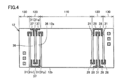
- FIG. 4 is a cross-sectional view showing a second modification of the multilayer substrate in FIG.
- the reinforcing layer 28 is provided along the inner and outer peripheral edges of the flexible portion 120 that changes the traveling direction by 180 ° in the folded portion 37.
- the reinforcing layer 28 is provided in a U-shaped line shape along the inner peripheral edge and the outer peripheral edge of the flexible portion 120.
- the multilayer substrate 10 in the present embodiment has a resin layer 21 made of a plurality of laminated resins having flexibility.
- the laminated body 12 which has is provided.
- the laminated body 12 is provided with a deformable flexible portion 120 that extends in a belt shape while repeatedly changing the traveling direction when viewed from the laminating direction of the resin layer 21.
- the flexible part 120 includes a folded part 37 at a position where the traveling direction is changed.
- the laminated body 12 is further provided with a metallic reinforcing layer 28 that is partially provided on the surface of the folded portion 37 when viewed from the laminating direction of the resin layer 21 and is not connected to any other electric circuit in the laminated body 12. Have.
- the multilayer substrate 10 can be obtained by improving the durability of the flexible portion 120 while sufficiently ensuring the flexibility of the flexible portion 120. Damage and delamination of the laminated resin layer 21 can be prevented.
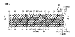
- FIG. 5 is a cross-sectional view showing a multilayer substrate according to Embodiment 2 of the present invention.
- FIG. 6 is a cross-sectional view showing the multilayer substrate along the line VI-VI in FIG.
- FIG. 5 shows a cross section of the multilayer substrate along the line VV in FIG.
- the multilayer substrate in the present embodiment basically has the same structure as that of the multilayer substrate 10 in the first embodiment. Hereinafter, the description of the overlapping structure will not be repeated.
- laminated body 12 is provided with main body portion 110, flexible portion 120, and pad portion 130.
- a flexible part 120 is provided on both sides of the main body part 110, and a pad part 130 is provided at a position where the periphery is taken into the flexible part 120.
- the flexible portion 120 extends in a strip shape while repeatedly changing the traveling direction by 90 ° when viewed from the stacking direction of the stacked body 12, and has a spiral shape as a whole.
- the flexible part 120 has, as its constituent parts, a folded part 37 disposed at a position where the traveling direction is changed, and an intermediate part 36 that connects between adjacent folded parts 37.
- the folded portion 37 and the intermediate portion 36 are alternately provided between the main body portion 110 and the pad portion 130. Folded portions 37 and intermediate portions 36 are alternately arranged from the main body portion 110 to the pad portion 130 while turning in a rectangular shape.
- returning part 37 is arrange
- the slit 12 for providing the deformable flexible part 120 is formed in the laminated body 12.
- the slit 31 penetrates in the laminating direction of the resin layer 21.
- the slit 31 extends while repeatedly changing the traveling direction by 90 ° when viewed from the stacking direction of the stacked body 12.
- the slit 31 is formed so that the flexible portions 120 adjacent to the spiral inner peripheral side and the outer peripheral side are separated from each other.
- a metal reinforcing layer 28 is provided on the folded portion 37.
- the reinforcing layer 28 is provided in a net shape on the surface of the folded portion 37 when viewed from the lamination direction of the resin layer 21.
- the form in which the reinforcing layer 28 is provided is the same as in the first embodiment.
- FIG. 7 is a cross-sectional view showing a first modification of the multilayer substrate in FIG.
- the multilayer substrate in the present modification is provided with reinforcing layer 28 in the same form as the multilayer substrate in FIG. 3 in the first embodiment.
- the reinforcing layer 28 is provided along the inner peripheral edge of the flexible portion 120 that changes the traveling direction by 90 ° in the folded portion 37.
- the reinforcing layer 28 is provided in an L-shaped line shape along the inner peripheral edge of the folded portion 37.
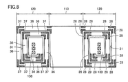
- FIG. 8 is a cross-sectional view showing a second modification of the multilayer substrate in FIG. Referring to FIG. 8, the multilayer substrate in the present modification is provided with reinforcing layer 28 in the same form as the multilayer substrate in FIG. 4 in the first embodiment.
- the reinforcing layer 28 is provided along the inner peripheral edge and the outer peripheral edge of the flexible portion 120 that changes the 90 ° traveling direction in the folded portion 37.
- the reinforcing layer 28 is provided in an L-shaped line shape along the inner and outer peripheral edges of the folded portion 37.
- the flexible portion 120 extending in a strip shape while repeatedly changing the traveling direction by 180 ° or 90 ° has been described.
- the present invention is not limited to this, and the flexible portion 120 is It may extend in a band shape while changing by another angle (for example, 60 °).
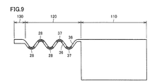
- FIG. 9 is a plan view showing a multilayer substrate according to Embodiment 3 of the present invention.
- the multilayer substrate in the present embodiment basically has the same structure as that of the multilayer substrate 10 in the first embodiment. Hereinafter, the description of the overlapping structure will not be repeated.
- laminated body 12 is provided with main body portion 110, flexible portion 120, and pad portion 130.
- the flexible part 120 extends linearly from the periphery of the main body part 110.
- the pad part 130 is provided at the tip of the flexible part 120 extending from the main body part 110.
- the structure in which the flexible part 120 extends from one place of the main body part 110 is shown, but the structure in which the flexible part 120 extends from a plurality of places in the main body part 110 is also possible. Good.
- the flexible portion 120 extends in a strip shape while repeatedly changing the traveling direction as seen from the lamination direction of the resin layer 21, and has a wave shape as a whole.
- the flexible part 120 has, as its constituent parts, a folded part 37 disposed at a position where the traveling direction is changed, and an intermediate part 36 that connects between adjacent folded parts 37.
- the flexible portion 120 may have a wave shape that extends in a curved shape in the folded portion 37 and linearly extends in the intermediate portion 36, or extends in a curved shape in the folded portion 37, and extends in a curved shape in the intermediate portion 36. It may have a wave shape.
- a metal reinforcing layer 28 is provided on the folded portion 37.
- the reinforcing layer 28 is provided in a net shape on the surface of the folded portion 37 when viewed from the lamination direction of the resin layer 21.
- the form in which the reinforcing layer 28 is provided is the same as in the first embodiment.
- This invention is mainly applied to a multilayer substrate having flexibility.
Landscapes
- Engineering & Computer Science (AREA)
- Microelectronics & Electronic Packaging (AREA)
- Structure Of Printed Boards (AREA)
- Production Of Multi-Layered Print Wiring Board (AREA)
Abstract
多層基板は、積層された複数の可撓性を有する樹脂からなる樹脂層を有する積層体(12)を備える。積層体(12)には、樹脂層の積層方向から見て、進行方向を繰り返し変化させながら帯状に延びる、変形可能な可撓部(120)が設けられる。可撓部(120)は、進行方向を変化させる位置に折り返し部(37)を含む。積層体(12)は、樹脂層(21)の積層方向から見た場合の折り返し部(37)の面上に部分的に設けられ、積層体(12)における他のいずれの電気回路とも接続されない金属性の補強層(28)をさらに有する。このような構成により、可撓部のフレキシブル性を確保しつつ、その耐久性を向上させた多層基板を提供する。
Description
この発明は、一般的には、多層基板に関し、より特定的には、積層された複数の樹脂層を有する積層体に、変形可能な可撓部が設けられた多層基板に関する。
従来の多層基板に関して、たとえば、特開2006-41044号公報には、高密度配線であっても、良好な屈曲性を確保し、しかも屈曲時における導体層の疲労を低減し、断線を防止し、高度の耐屈曲性を実現することを目的とした、多層フレキシブル配線回路基板が開示されている(特許文献1)。特許文献1に開示された多層フレキシブル配線回路基板においては、2つのフレキシブル配線回路基板が積層される層間にエアギャップが設けられている。屈曲時にエアギャップの端部に集中する応力を受けるため、フレキシブル配線回路基板の表面に補強層が形成されている。
上述の特許文献に開示されるように、折り畳み可能な携帯電話機などの電気機器に、フレキシブル(変形可能)な可撓部が設けられた多層基板が用いられている。このような多層基板においては、変形に伴って可撓部の特定個所に応力が集中し易いため、可撓部の耐久性が損なわれる。一方、可撓部の耐久性を向上させる手段として、可撓部に補強を加えることが考えられる。しかしながら、補強の方法によっては、可撓部のフレキシブル性が大きく損なわれる懸念がある。
そこでこの発明の目的は、上記の課題を解決することであり、可撓部のフレキシブル性を確保しつつ、その耐久性を向上させた多層基板を提供することである。
この発明に従った多層基板は、積層された複数の可撓性を有する樹脂からなる樹脂層を有する積層体を備える。積層体には、樹脂層の積層方向から見て、進行方向を繰り返し変化させながら帯状に延びる、変形可能な可撓部が設けられる。可撓部は、進行方向を変化させる位置に折り返し部を含む。積層体は、樹脂層の積層方向から見た場合の折り返し部の面上に部分的に設けられ、積層体における他のいずれの電気回路とも接続されない金属性の補強層をさらに有する。
このように構成された多層基板によれば、可撓部の変形に伴って応力が集中し易い折り返し部に金属製の補強層を設けることによって、可撓部の耐久性を向上させることができる。この際、補強層は、樹脂層の積層方向から見た場合の折り返し部の面上に部分的に設けられるため、可撓部のフレキシブル性が損なわれることを抑制できる。
また好ましくは、補強層は、複数の樹脂層の層間に介挿される。このように構成された多層基板によれば、積層体の内部構造によって、可撓部の耐久性を向上させることができる。
また好ましくは、補強部は、網状に設けられる。このように構成された多層基板によれば、可撓部の変形時に折り返し部に作用する応力の方向にかかわらず、可撓部の耐久性を向上させることができる。
また好ましくは、可撓部は、全体としてミアンダ形状をなすように、進行方向を繰り返し180°反転させながら帯状に延びる。
このように構成された多層基板によれば、全体としてミアンダ形状をなす可撓部のフレキシブル性を確保しつつ、その耐久性を向上させることができる。
また好ましくは、可撓部は、全体として螺旋形状をなすように、進行方向を繰り返し90°ずつ変化させながら帯状に延びる。
このように構成された多層基板によれば、全体として螺旋形状をなす可撓部のフレキシブル性を確保しつつ、その耐久性を向上させることができる。
また好ましくは、補強層は、折り返し部において進行方向を変化させる可撓部の内周縁に沿って設けられる。
このように構成された多層基板によれば、折り返し部のうちでも応力がより集中し易い内周縁に補強層を設けることによって、可撓部のフレキシブル性を十分に確保しつつ、その耐久性を効率的に向上させることができる。
さらに好ましくは、補強層は、折り返し部において進行方向を変化させる可撓部の外周縁に沿ってさらに設けられる。
このように構成された多層基板によれば、可撓部の耐久性をさらに向上させることができる。
また好ましくは、積層体は、補強層と同じ層に設けられる配線層をさらに有する。
このように構成された多層基板によれば、補強層を配線層と同じプロセスで形成することが可能となる。
このように構成された多層基板によれば、補強層を配線層と同じプロセスで形成することが可能となる。
以上に説明したように、この発明に従えば、可撓部のフレキシブル性を確保しつつ、その耐久性を向上させた多層基板を提供することができる。
この発明の実施の形態について、図面を参照して説明する。なお、以下で参照する図面では、同一またはそれに相当する部材には、同じ番号が付されている。
(実施の形態1)
図1は、この発明の実施の形態1における多層基板を示す断面図である。図2は、図1中のII-II線上に沿った多層基板を示す断面図である。図1には、図2中のI-I線上に沿った多層基板の断面が示されている。
図1は、この発明の実施の形態1における多層基板を示す断面図である。図2は、図1中のII-II線上に沿った多層基板を示す断面図である。図1には、図2中のI-I線上に沿った多層基板の断面が示されている。
図1および図2を参照して、まず、本実施の形態における多層基板10の全体構造について説明すると、多層基板10は、複数の樹脂層21A,21B,21C,21D,21E,21F(以下、特に区別しない場合には、樹脂層21という)と、複数の配線層26G,26H,26I,26J,26K(以下、特に区別しない場合には、配線層26という)と、インナービア27とからなる積層体12を有する。
樹脂層21は、熱可塑性樹脂から形成されている。樹脂層21は、たとえば、ポリイミド、LCP(液晶ポリマ)、PEEK(ポリエーテルエーテルケトン)、PPS(ポリフェニレンサルファイド)から形成されている。複数の樹脂層21は、図1中の矢印101に示す方向に積層されている(以下、矢印101に示す方向を樹脂層21の積層方向という)。樹脂層21A、樹脂層21B、樹脂層21C、樹脂層21D、樹脂層21Eおよび樹脂層21Fは、挙げた順に上から下に並んでいる。積層された複数の樹脂層21は、積層体12の外観をなしている。
配線層26は、銅、銀、アルミニウム、ステンレス、ニッケルまたは金などの金属や、これらの金属を含む合金などから形成されている金属膜である。具体的には、配線層26は、たとえば、銅箔などの金属箔である。配線層26は、積層体12の内部に設けられている。配線層26は、複数の樹脂層21の層間に配置されている。より具体的には、配線層26Gは、樹脂層21Aおよび樹脂層21Bの層間に配置され、配線層26Hは、樹脂層21Bおよび樹脂層21Cの層間に配置され、配線層26Iは、樹脂層21Cおよび樹脂層21Dの層間に配置され、配線層26Jは、樹脂層21Dおよび樹脂層21Eの層間に配置され、配線層26Kは、樹脂層21Eおよび樹脂層21Fの層間に配置されている。
配線層26は、所定のパターン形状に形成されており、ストリップラインやマイクロストリップライン、コイル、コンデンサなどの各種の電気回路を形成している。
インナービア27は、導電性材料から形成されている。インナービア27は、積層体12の内部に設けられている。インナービア27は、樹脂層21の積層方向に延びて、異なる層に設けられた配線層26の間を互いに接続している。
なお、図中には、積層体12が樹脂層21の積層方向から見て矩形形状の平面視を有する場合が示されているが、積層体12は、矩形以外の任意の形状の平面視を有してもよい。また、図中には、積層体12の内部に設けられた配線層26のみが示されているが、積層体12の表面にも配線層26が設けられてもよい。
積層体12には、本体部110、可撓部120およびパッド部130が設けられている。本実施の形態では、本体部110を中心にその両側に、可撓部120およびパッド部130が挙げた順に並ぶ。
本体部110は、可撓部120よりも変形し難いリジッドな部分である。本体部110の表面には、各種の電気部品が実装されてもよい。可撓部120は、変形可能なフレキシブルな部分である。積層体12を平面的に見て、可撓部120は、本体部110の周縁から延出している。パッド部130は、本体部110から延出する可撓部120の先端に設けられている。パッド部130には、積層体12に設けられた配線と外部回路とを接続するための電気接続用のコネクタが設けられてもよい。
本実施の形態では、可撓部120は、樹脂層21の積層方向(図1中の矢印101に示す方向)および本体部110とパッド部130とを結ぶ方向(図2中の矢印102に示す方向、伸縮方向)の両方に変形可能に設けられている。このような可撓部120が有するフレキシブル性によって、本体部110とパッド部130との間に高低差が生じるような部位や、本体部110とパッド部130との間の距離が変化するような部位への多層基板10の実装が可能となる。また、高さのばらつきや実装長さのばらつきが生じる部位に対しても、多層基板10の実装が可能となる。
なお、可撓部120のフレキシブル性を増すために、可撓部120における樹脂層21の層数を、本体部110における樹脂層21の層数よりも少なくしてもよい。
積層体12には、変形可能な可撓部120を設けるための複数本のスリット31p,31q,31rが形成されている(以下、特に区別しない場合には、スリット31という)。
可撓部120は、樹脂層21の積層方向から見て、進行方向を繰り返し変化させながら帯状に延びており、本実施の形態では、全体として波形状をなしている。可撓部120は、その構成部位として、進行方向を変化させる位置に配置される折り返し部37と、隣り合う折り返し部37の間を繋ぐ中間部36とを有する。
折り返し部37および中間部36は、本体部110とパッド部130との間で交互に設けられている。本実施の形態では、可撓部120が、3つの折り返し部37および2つの中間部36から構成されており、これらの両端に配置された折り返し部37がそれぞれ本体部110およびパッド部130に接続されている。
図2中の可撓部120に、その進行方向に沿って延びる中心線を描いた場合、中心線は、折り返し部37に腹が配置される波形状をなす。
特に本実施の形態では、可撓部120が、樹脂層21の積層方向から見て、進行方向を繰り返し180°反転させながら帯状に延びることにより、全体としてミアンダ形状をなしている。可撓部120のその進行方向に沿って延びる中心線は、矩形波の形状をなしている。
積層体12に形成されたスリット31は、樹脂層21の積層方向に貫通する。樹脂層21の積層方向から見て、スリット31は、中間部36の進行方向に沿って折り返し部37に向けて延びている。スリット31は、直線状に延びている。複数本のスリット31は、互いに平行に延びている。複数本のスリット31は、本体部110とパッド部130とを結ぶ方向に互いに間隔を設けて形成されている。
スリット31p、スリット31qおよびスリット31rは、挙げた順に、本体部110側からパッド部130側に並んでいる。積層体12は、端辺12aと、端辺12aと対向して配置される端辺12bとを有する。スリット31pは、端辺12bから端辺12aの手前まで直線状に延びている。スリット31qは、端辺12aから端辺12bの手前まで直線状に延びている。スリット31rは、端辺12bから端辺12aの手前まで直線状に延びている。
直線状に延びるスリット31p,31q,31rの先端には、折り返し部37が設けられている。スリット31pとスリット31qとの間およびスリット31qとスリット31rとの間には、中間部36が設けられている。
可撓部120は、積層体12に、端辺12aから端辺12bの手前まで延びるスリット31と、端辺12bから端辺12aの手前まで延びるスリット31とが交互に形成されることによって、ミアンダ形状に形成されている。
本実施の形態における多層基板10においては、積層体12が、金属製の補強層28をさらに有する。
補強層28は、折り返し部37に設けられている。補強層28は、樹脂層21の積層方向から見た場合の折り返し部37の面上に部分的に設けられている。本実施の形態では、補強層28が、樹脂層21の積層方向から見た場合の折り返し部37の面上に網状に設けられている。
なお、図2中には、網状に設けられる場合の一形態として、矩形の格子構造の補強層28が示されているが、このような形態に限られず、たとえば三角形のトラス構造や六角形のハニカム構造の補強層28が設けられてもよい。
補強層28は、積層体12の内部に設けられている。補強層28は、複数の樹脂層21の層間に介挿されている。本実施の形態では、補強層28が、樹脂層21Aおよび樹脂層21Bの層間と、樹脂層21Eおよび樹脂層21Fの層間とに配置されている。補強層28は、配線層26を形成する工程と同時に形成されている。配線層26Gは、樹脂層21Aおよび樹脂層21Bの層間に配置された補強層28と同じ層に設けられ、配線層26Kは、樹脂層21Eおよび樹脂層21Fの層間に配置された補強層28と同じ層に設けられている。
補強層28は、たとえば、銅、銀、アルミニウム、ステンレス、ニッケルまたは金などの金属や、これらの金属を含む合金などから形成されている。補強層28は、同じ層に設けられた配線層26と同一の金属から形成されている。
補強層28は、積層体12における他のいずれの電気回路とも接続されないように設けられている。補強層28は、いずれの配線層26とも接触することなく設けられている。補強層28の周囲は、絶縁性の樹脂層21によって取り囲まれている。なお、補強層28は、複数層に跨って形成されていてもよい。また、複数層に跨って形成された補強層28同士を、ダミーのインナービアによって接続してもよい。
このような構成によれば、可撓部120の変形に伴って壁開の力が働き、応力が集中し易い折り返し部37に金属製の補強層28が設けられるため、可撓部120の耐久性を向上させることができる。これにより、多層基板10の破損や、積層された樹脂層21の層間剥離を防止できる。
また、補強層28は、折り返し部37の面上に部分的に設けられるため、補強層28の設置に起因して可撓部120のフレキシブル性が大きく損なわれることを防止できる。さらに、補強層28が設けられる折り返し部37においても、隣接する樹脂層21の樹脂同士が接触する領域が確保されるため、積層された樹脂層21の層間剥離をより確実に防ぐことができる。
また、補強層28は、積層体12における他のいずれの電気回路とも接続されず、ダミーの配線層として設けられる。このため、多層基板10の特性に影響を与えることなく、可撓部120の耐久性の向上を図ることができる。
なお、本実施の形態では、補強層28を複数の樹脂層21の層間に設けたが、このような形態に限られず、補強層28を積層体12の表面に設けてもよい。
本実施の形態における多層基板10は、たとえば、以下に説明する製造工程により製造される。まず、銅箔付きの樹脂シートを準備する。次に、所定形状にパターニングしたレジストをマスクとして用いて、銅箔部分を酸(一例として、HCl)によりエッチングする。この際、配線層26および補強層28を同じプロセスにより形成する。すなわち、配線層26のパターニングおよび補強層28のパターニングを同じエッチングのプロセスにより実施する。次に、アルカリ(一例として、NaOH)によりレジストを剥離し、引き続き中和処理を行なう。
次に、インナービア27に対応する箇所に、レーザによる孔あけ加工を実施する。形成された孔に導電性ペーストを充填する。次に、以上の工程を経た複数枚の樹脂シートを重ね合わせ、熱圧着することによって積層体12を得る。最後に、レーザ加工、ダイシング加工またはパンチ加工により、積層体12にスリット31を形成する。
本実施の形態では、補強層28が配線層26と同じプロセスにより形成されるため、多層基板10の製造工程を増やすことなく、積層体12に補強層28を設けることができる。
続いて、図2中の多層基板の各種変形例について説明する。図3は、図2中の多層基板の第1変形例を示す断面図である。
図3を参照して、本変形例では、補強層28が、折り返し部37において180°進行方向を変化させる可撓部120の内周縁に沿って設けられている。補強層28は、可撓部120の内周縁に沿ってU字形のライン状に設けられている。
このような構成によれば、補強層28が、折り返し部37においても応力がより集中し易い可撓部120の内周縁に設けられる。これにより、可撓部120のフレキシブル性を十分に確保しつつ、その耐久性を効率的に向上させることができる。
図4は、図2中の多層基板の第2変形例を示す断面図である。図4を参照して、本変形例では、補強層28が、折り返し部37において180°進行方向を変化させる可撓部120の内周縁および外周縁に沿って設けられている。補強層28は、可撓部120の内周縁および外周縁に沿ってそれぞれU字形のライン状に設けられている。
このような構成によれば、可撓部120のフレキシブル性を十分に確保しつつ、可撓部120の耐久性をさらに向上させることができる。
なお、折り返し部37に設けられる補強層28を網状とした場合、可撓部120の幅方向の全領域に渡って補強を施すことが可能となり、補強されていない柔軟性の高い特定部位が生じることを回避できる。このため、折り返し部37に配索された配線層26の配線間距離が可撓部120の変形時に接近するなどして、特性変動が発生することを防止できる。
以上に説明した、この発明の実施の形態1における多層基板の構造についてまとめて説明すると、本実施の形態における多層基板10は、積層された複数の可撓性を有する樹脂からなる樹脂層21を有する積層体12を備える。積層体12には、樹脂層21の積層方向から見て、進行方向を繰り返し変化させながら帯状に延びる、変形可能な可撓部120が設けられる。可撓部120は、進行方向を変化させる位置に折り返し部37を含む。積層体12は、樹脂層21の積層方向から見た場合の折り返し部37の面上に部分的に設けられ、積層体12における他のいずれの電気回路とも接続されない金属性の補強層28をさらに有する。
このように構成された、この発明の実施の形態1における多層基板10によれば、可撓部120のフレキシブル性を十分に確保しつつ、可撓部120の耐久性の向上によって、多層基板10の破損や積層された樹脂層21の層間剥離を防ぐことができる。
(実施の形態2)
図5は、この発明の実施の形態2における多層基板を示す断面図である。図6は、図5中のVI-VI線上に沿った多層基板を示す断面図である。図5には、図6中のV-V線上に沿った多層基板の断面が示されている。本実施の形態における多層基板は、実施の形態1における多層基板10と比較して、基本的には同様の構造を備える。以下、重複する構造についてはその説明を繰り返さない。
図5は、この発明の実施の形態2における多層基板を示す断面図である。図6は、図5中のVI-VI線上に沿った多層基板を示す断面図である。図5には、図6中のV-V線上に沿った多層基板の断面が示されている。本実施の形態における多層基板は、実施の形態1における多層基板10と比較して、基本的には同様の構造を備える。以下、重複する構造についてはその説明を繰り返さない。
図5および図6を参照して、本実施の形態では、積層体12に、本体部110、可撓部120およびパッド部130が設けられている。本体部110の両側に可撓部120が設けられ、その可撓部120に周囲を取り込まれた位置にパッド部130が設けられている。
可撓部120は、積層体12の積層方向から見て、90°ずつ進行方向を繰り返し変化させながら帯状に延びており、全体として螺旋形状をなしている。可撓部120は、その構成部位として、進行方向を変化させる位置に配置される折り返し部37と、隣り合う折り返し部37の間を繋ぐ中間部36とを有する。
折り返し部37および中間部36は、本体部110とパッド部130との間で交互に設けられている。本体部110から折り返し部37および中間部36が交互に並んで矩形状に旋回しながらパッド部130へと連なっている。折り返し部37は、その矩形状に旋回する角部に配置され、中間部36は、隣り合う角部間の直線部に配置されている。
積層体12には、変形可能な可撓部120を設けるためのスリット31が形成されている。スリット31は、樹脂層21の積層方向に貫通する。スリット31は、積層体12の積層方向から見て、90°ずつ進行方向を繰り返し変化させながら延びている。スリット31は、螺旋形状の内周側と外周側とに隣り合う可撓部120同士を互いに離間させるように形成されている。
本実施の形態における多層基板においては、金属製の補強層28が、折り返し部37に設けられている。補強層28は、樹脂層21の積層方向から見た場合の折り返し部37の面上に網状に設けられている。そのほか、補強層28が設けられる形態は、実施の形態1と同様である。
図7は、図6中の多層基板の第1変形例を示す断面図である。図7を参照して、本変形例における多層基板では、実施の形態1における図3中の多層基板と同様の形態で、補強層28が設けられている。
すなわち、補強層28は、折り返し部37において90°進行方向を変化させる可撓部120の内周縁に沿って設けられている。補強層28は、折り返し部37の内周縁に沿ってL字形のライン状に設けられている。
図8は、図6中の多層基板の第2変形例を示す断面図である。図8を参照して、本変形例における多層基板では、実施の形態1における図4中の多層基板と同様の形態で、補強層28が設けられている。
すなわち、補強層28は、折り返し部37において90°進行方向を変化させる可撓部120の内周縁および外周縁に沿って設けられている。補強層28は、折り返し部37の内周縁および外周縁に沿ってL字形のライン状に設けられている。
このように構成された、この発明の実施の形態2における多層基板によれば、実施の形態1に記載の効果を同様に奏することができる。
なお、以上に説明した実施の形態1および2では、進行方向を繰り返し180°または90°ずつ変化させながら帯状に延びる可撓部120について説明したが、これに限られず、可撓部120は、他の角度(たとえば、60°)だけ変化しながら帯状に延びてもよい。
(実施の形態3)
図9は、この発明の実施の形態3における多層基板を示す平面図である。本実施の形態における多層基板は、実施の形態1における多層基板10と比較して、基本的には同様の構造を備える。以下、重複する構造についてはその説明を繰り返さない。
図9は、この発明の実施の形態3における多層基板を示す平面図である。本実施の形態における多層基板は、実施の形態1における多層基板10と比較して、基本的には同様の構造を備える。以下、重複する構造についてはその説明を繰り返さない。
図9を参照して、本実施の形態における多層基板においては、積層体12に、本体部110、可撓部120およびパッド部130が設けられている。可撓部120は、本体部110の周縁から線状に延出している。パッド部130は、本体部110から延出する可撓部120の先端に設けられている。
なお、図中には、本体部110の1個所から可撓部120が延出する構造が示されているが、本体部110の複数個所から可撓部120が延出する構造であってもよい。
可撓部120は、樹脂層21の積層方向から見て、進行方向を繰り返し変化させながら帯状に延びており、全体として波形状をなしている。可撓部120は、その構成部位として、進行方向を変化させる位置に配置される折り返し部37と、隣り合う折り返し部37の間を繋ぐ中間部36とを有する。可撓部120は、折り返し部37において湾曲状に延び、中間部36において直線状に延びる波形状を有してもよいし、折り返し部37において湾曲状に延び、中間部36において湾曲状に延びる波形状を有してもよい。
本実施の形態における多層基板においては、金属製の補強層28が、折り返し部37に設けられている。補強層28は、樹脂層21の積層方向から見た場合の折り返し部37の面上に網状に設けられている。そのほか、補強層28が設けられる形態は、実施の形態1と同様である。
このように構成された、この発明の実施の形態3における多層基板によれば、実施の形態1に記載の効果を同様に奏することができる。
今回開示された実施の形態はすべての点で例示であって制限的なものではないと考えられるべきである。本発明の範囲は上記した説明ではなくて請求の範囲によって示され、請求の範囲と均等の意味および範囲内でのすべての変更が含まれることが意図される。
この発明は、主に、可撓(フレキシブル)性を備えた多層基板に適用される。
10 多層基板、12 積層体、12a,12b 端辺、21,21A,21B,21C,21D,21E,21F 樹脂層、26,26G,26H,26I,26J,26K 配線層、27 インナービア、28 補強層、31,31p,31q,31r スリット、36 中間部、37 折り返し部、110 本体部、120 折り返し部、130 パッド部。
Claims (8)
- 積層された複数の可撓性を有する樹脂からなる樹脂層を有する積層体を備え、
前記積層体には、前記樹脂層の積層方向から見て、進行方向を繰り返し変化させながら帯状に延びる、変形可能な可撓部が設けられ、
前記可撓部は、進行方向を変化させる位置に折り返し部を含み、
前記積層体は、前記樹脂層の積層方向から見た場合の前記折り返し部の面上に部分的に設けられ、前記積層体における他のいずれの電気回路とも接続されない金属性の補強層をさらに有する、多層基板。 - 前記補強層は、複数の前記樹脂層の層間に介挿される、請求項1に記載の多層基板。
- 前記補強部は、網状に設けられる、請求項1または2に記載の多層基板。
- 前記可撓部は、全体としてミアンダ形状をなすように、進行方向を繰り返し180°反転させながら帯状に延びる、請求項1から3のいずれか1項に記載の多層基板。
- 前記可撓部は、全体として螺旋形状をなすように、進行方向を繰り返し90°ずつ変化させながら帯状に延びる、請求項1から4のいずれか1項に記載の多層基板。
- 前記補強層は、前記折り返し部において進行方向を変化させる前記可撓部の内周縁に沿って設けられる、請求項4または5に記載の多層基板。
- 前記補強層は、前記折り返し部において進行方向を変化させる前記可撓部の外周縁に沿ってさらに設けられる、請求項6に記載の多層基板。
- 前記積層体は、前記補強層と同じ層に設けられる配線層をさらに有する、請求項1から7のいずれか1項に記載の多層基板。
Priority Applications (1)
| Application Number | Priority Date | Filing Date | Title |
|---|---|---|---|
| JP2015535397A JP6065119B2 (ja) | 2013-09-05 | 2014-08-07 | 多層基板 |
Applications Claiming Priority (2)
| Application Number | Priority Date | Filing Date | Title |
|---|---|---|---|
| JP2013-183891 | 2013-09-05 | ||
| JP2013183891 | 2013-09-05 |
Publications (1)
| Publication Number | Publication Date |
|---|---|
| WO2015033736A1 true WO2015033736A1 (ja) | 2015-03-12 |
Family
ID=52628219
Family Applications (1)
| Application Number | Title | Priority Date | Filing Date |
|---|---|---|---|
| PCT/JP2014/070901 Ceased WO2015033736A1 (ja) | 2013-09-05 | 2014-08-07 | 多層基板 |
Country Status (2)
| Country | Link |
|---|---|
| JP (1) | JP6065119B2 (ja) |
| WO (1) | WO2015033736A1 (ja) |
Cited By (11)
| Publication number | Priority date | Publication date | Assignee | Title |
|---|---|---|---|---|
| WO2016163258A1 (ja) * | 2015-04-09 | 2016-10-13 | ソニー株式会社 | 可撓性デバイス |
| WO2017126243A1 (ja) * | 2016-01-20 | 2017-07-27 | 株式会社村田製作所 | 樹脂多層基板、および、電子機器 |
| DE102016117795A1 (de) * | 2016-09-21 | 2018-03-22 | Endress+Hauser Conducta Gmbh+Co. Kg | Feldgerät der Prozessautomatisierungstechnik |
| DE102017200414A1 (de) | 2017-01-12 | 2018-09-13 | Ifm Electronic Gmbh | Messgerät für die Prozess- und Automatisierungstechnik |
| WO2019224901A1 (ja) * | 2018-05-22 | 2019-11-28 | 株式会社メイコーテクノ | フレキシブル部を有するリジッドプリント配線基板 |
| WO2020137148A1 (ja) * | 2018-12-26 | 2020-07-02 | ソニー株式会社 | フレキシブル配線基板及び電子機器 |
| JP2020136654A (ja) * | 2019-02-22 | 2020-08-31 | サムソン エレクトロ−メカニックス カンパニーリミテッド. | プリント回路基板及びこれを備えたカメラモジュール |
| US20220240381A1 (en) * | 2021-01-25 | 2022-07-28 | Beijing Boe Optoelectronics Technology Co., Ltd. | Flexible printed circuit and manufacturing method thereof, and displaying device |
| JP7562257B2 (ja) | 2017-01-19 | 2024-10-07 | コンティ テミック マイクロエレクトロニック ゲゼルシャフト ミット ベシュレンクテル ハフツング | 電子モジュール、特に乗物搭載用に構成されるカメラのモジュール接続用可撓性導体トラック |
| CN119584411A (zh) * | 2024-11-20 | 2025-03-07 | 深圳市正佳兴电子有限公司 | 一种双层柔性线路板 |
| US20250203770A1 (en) * | 2023-12-19 | 2025-06-19 | Chipbond Technology Corporation | Flexible circuit board |
Citations (6)
| Publication number | Priority date | Publication date | Assignee | Title |
|---|---|---|---|---|
| JPH11219623A (ja) * | 1998-02-03 | 1999-08-10 | Japan Aviation Electronics Ind Ltd | 配線自由度の高い可撓配線部材 |
| JP2003258389A (ja) * | 2002-03-06 | 2003-09-12 | Sumitomo Electric Printed Circuit Inc | フレキシブルプリント配線板 |
| JP2003283061A (ja) * | 2002-03-27 | 2003-10-03 | Kojima Press Co Ltd | フレキシブルプリント配線基板 |
| JP2004071562A (ja) * | 2002-08-01 | 2004-03-04 | Yazaki Corp | フレキシブルな導電要素 |
| JP2007103695A (ja) * | 2005-10-05 | 2007-04-19 | Sumitomo Bakelite Co Ltd | フレキシブルプリント基板及び電子機器 |
| JP2007281378A (ja) * | 2006-04-11 | 2007-10-25 | Sharp Corp | フレキシブル配線基板および電子部品 |
Family Cites Families (11)
| Publication number | Priority date | Publication date | Assignee | Title |
|---|---|---|---|---|
| JPS6057152U (ja) * | 1983-04-28 | 1985-04-20 | 株式会社東芝 | プリント配線板 |
| JPH04137592A (ja) * | 1990-09-27 | 1992-05-12 | Toshiba Lighting & Technol Corp | 多層回路基板 |
| JPH09205257A (ja) * | 1995-08-30 | 1997-08-05 | Toshiba Corp | フレキシブルプリント配線板 |
| JP2001053393A (ja) * | 1999-08-06 | 2001-02-23 | Fujikura Ltd | フレキシブル回路基板及びそれを用いた光ピックアップ装置 |
| TW533750B (en) * | 2001-11-11 | 2003-05-21 | Solidlite Corp | LED lamp |
| CN101754572B (zh) * | 2008-12-02 | 2012-01-11 | 富士迈半导体精密工业(上海)有限公司 | 硬性电路板、电路板组件及电路板模组 |
| TWI484873B (zh) * | 2009-04-07 | 2015-05-11 | Au Optronics Corp | 軟性電路板 |
| JP2011018665A (ja) * | 2009-07-07 | 2011-01-27 | Murata Mfg Co Ltd | 回路基板 |
| JP2011249637A (ja) * | 2010-05-28 | 2011-12-08 | Molex Inc | 回路基板アッセンブリ |
| EP2640168A1 (en) * | 2012-03-15 | 2013-09-18 | Nederlandse Organisatie voor toegepast-natuurwetenschappelijk Onderzoek TNO | Submount, assembly including submount, method of assembling and assembling device |
| WO2014045862A1 (ja) * | 2012-09-24 | 2014-03-27 | 株式会社村田製作所 | フレキシブル多層基板 |
-
2014
- 2014-08-07 WO PCT/JP2014/070901 patent/WO2015033736A1/ja not_active Ceased
- 2014-08-07 JP JP2015535397A patent/JP6065119B2/ja active Active
Patent Citations (6)
| Publication number | Priority date | Publication date | Assignee | Title |
|---|---|---|---|---|
| JPH11219623A (ja) * | 1998-02-03 | 1999-08-10 | Japan Aviation Electronics Ind Ltd | 配線自由度の高い可撓配線部材 |
| JP2003258389A (ja) * | 2002-03-06 | 2003-09-12 | Sumitomo Electric Printed Circuit Inc | フレキシブルプリント配線板 |
| JP2003283061A (ja) * | 2002-03-27 | 2003-10-03 | Kojima Press Co Ltd | フレキシブルプリント配線基板 |
| JP2004071562A (ja) * | 2002-08-01 | 2004-03-04 | Yazaki Corp | フレキシブルな導電要素 |
| JP2007103695A (ja) * | 2005-10-05 | 2007-04-19 | Sumitomo Bakelite Co Ltd | フレキシブルプリント基板及び電子機器 |
| JP2007281378A (ja) * | 2006-04-11 | 2007-10-25 | Sharp Corp | フレキシブル配線基板および電子部品 |
Cited By (16)
| Publication number | Priority date | Publication date | Assignee | Title |
|---|---|---|---|---|
| WO2016163258A1 (ja) * | 2015-04-09 | 2016-10-13 | ソニー株式会社 | 可撓性デバイス |
| WO2017126243A1 (ja) * | 2016-01-20 | 2017-07-27 | 株式会社村田製作所 | 樹脂多層基板、および、電子機器 |
| JPWO2017126243A1 (ja) * | 2016-01-20 | 2018-06-14 | 株式会社村田製作所 | 樹脂多層基板、および、電子機器 |
| JP2018170521A (ja) * | 2016-01-20 | 2018-11-01 | 株式会社村田製作所 | 樹脂多層基板と回路基板の接合構造 |
| US10403989B2 (en) | 2016-01-20 | 2019-09-03 | Murata Manufacturing Co., Ltd. | Resin multilayer substrate and electronic device |
| DE102016117795A1 (de) * | 2016-09-21 | 2018-03-22 | Endress+Hauser Conducta Gmbh+Co. Kg | Feldgerät der Prozessautomatisierungstechnik |
| DE102017200414A1 (de) | 2017-01-12 | 2018-09-13 | Ifm Electronic Gmbh | Messgerät für die Prozess- und Automatisierungstechnik |
| JP7562257B2 (ja) | 2017-01-19 | 2024-10-07 | コンティ テミック マイクロエレクトロニック ゲゼルシャフト ミット ベシュレンクテル ハフツング | 電子モジュール、特に乗物搭載用に構成されるカメラのモジュール接続用可撓性導体トラック |
| JPWO2019224901A1 (ja) * | 2018-05-22 | 2020-05-28 | 株式会社メイコーテクノ | フレキシブル部を有するリジッドプリント配線基板 |
| WO2019224901A1 (ja) * | 2018-05-22 | 2019-11-28 | 株式会社メイコーテクノ | フレキシブル部を有するリジッドプリント配線基板 |
| WO2020137148A1 (ja) * | 2018-12-26 | 2020-07-02 | ソニー株式会社 | フレキシブル配線基板及び電子機器 |
| JP2020136654A (ja) * | 2019-02-22 | 2020-08-31 | サムソン エレクトロ−メカニックス カンパニーリミテッド. | プリント回路基板及びこれを備えたカメラモジュール |
| US20220240381A1 (en) * | 2021-01-25 | 2022-07-28 | Beijing Boe Optoelectronics Technology Co., Ltd. | Flexible printed circuit and manufacturing method thereof, and displaying device |
| US11839025B2 (en) * | 2021-01-25 | 2023-12-05 | Beijing Boe Optoelectronics Technology Co., Ltd. | Flexible printed circuit and manufacturing method thereof, and displaying device |
| US20250203770A1 (en) * | 2023-12-19 | 2025-06-19 | Chipbond Technology Corporation | Flexible circuit board |
| CN119584411A (zh) * | 2024-11-20 | 2025-03-07 | 深圳市正佳兴电子有限公司 | 一种双层柔性线路板 |
Also Published As
| Publication number | Publication date |
|---|---|
| JP6065119B2 (ja) | 2017-01-25 |
| JPWO2015033736A1 (ja) | 2017-03-02 |
Similar Documents
| Publication | Publication Date | Title |
|---|---|---|
| JP5924456B2 (ja) | 多層基板 | |
| JP6065119B2 (ja) | 多層基板 | |
| US9485860B2 (en) | Multilayer board | |
| JP3173143U (ja) | 高周波信号線路 | |
| CN219204859U (zh) | 多层基板 | |
| JP6737246B2 (ja) | 多層基板 | |
| JP2010103388A (ja) | 積層フレキシブル配線基板、その製造方法、及びそれを用いたrfid用電子タグのアンテナ | |
| JP6259813B2 (ja) | 樹脂多層基板、および樹脂多層基板の製造方法 | |
| US9847171B2 (en) | Flexible cable and electronic device | |
| CN213124101U (zh) | 多层基板以及多层基板的安装构造 | |
| CN205646089U (zh) | 信号线路 | |
| CN207560432U (zh) | 多层基板 | |
| JP5637340B2 (ja) | フラットケーブル | |
| CN114788425B (zh) | 布线电路基板和其制造方法 | |
| JP5741975B2 (ja) | 樹脂多層基板 | |
| JP2015046463A (ja) | フレキシブル配線基板 | |
| CN204425772U (zh) | 多层基板 | |
| CN111149177B (zh) | 电感器及其制造方法 | |
| CN211828497U (zh) | 树脂多层基板以及电子设备 | |
| JP2015026747A (ja) | 樹脂多層基板 | |
| WO2014065172A1 (ja) | フレキシブル基板 | |
| JP2025182679A (ja) | 少なくとも2つのフレキシブル配線板又は配線板セグメントの電気的及び機械的接続方法 | |
| JP6089614B2 (ja) | 樹脂多層基板 | |
| JP5958122B2 (ja) | 高周波信号線路及び信号線路付き基材層の製造方法 | |
| JPWO2022113779A5 (ja) |
Legal Events
| Date | Code | Title | Description |
|---|---|---|---|
| 121 | Ep: the epo has been informed by wipo that ep was designated in this application |
Ref document number: 14841823 Country of ref document: EP Kind code of ref document: A1 |
|
| ENP | Entry into the national phase |
Ref document number: 2015535397 Country of ref document: JP Kind code of ref document: A |
|
| NENP | Non-entry into the national phase |
Ref country code: DE |
|
| 122 | Ep: pct application non-entry in european phase |
Ref document number: 14841823 Country of ref document: EP Kind code of ref document: A1 |