WO2015033638A1 - 半導体発光素子 - Google Patents
半導体発光素子 Download PDFInfo
- Publication number
- WO2015033638A1 WO2015033638A1 PCT/JP2014/065322 JP2014065322W WO2015033638A1 WO 2015033638 A1 WO2015033638 A1 WO 2015033638A1 JP 2014065322 W JP2014065322 W JP 2014065322W WO 2015033638 A1 WO2015033638 A1 WO 2015033638A1
- Authority
- WO
- WIPO (PCT)
- Prior art keywords
- layer
- light emitting
- substrate
- modified
- semiconductor light
- Prior art date
- Legal status (The legal status is an assumption and is not a legal conclusion. Google has not performed a legal analysis and makes no representation as to the accuracy of the status listed.)
- Ceased
Links
Images




Classifications
-
- H—ELECTRICITY
- H10—SEMICONDUCTOR DEVICES; ELECTRIC SOLID-STATE DEVICES NOT OTHERWISE PROVIDED FOR
- H10H—INORGANIC LIGHT-EMITTING SEMICONDUCTOR DEVICES HAVING POTENTIAL BARRIERS
- H10H20/00—Individual inorganic light-emitting semiconductor devices having potential barriers, e.g. light-emitting diodes [LED]
- H10H20/80—Constructional details
- H10H20/81—Bodies
- H10H20/819—Bodies characterised by their shape, e.g. curved or truncated substrates
- H10H20/82—Roughened surfaces, e.g. at the interface between epitaxial layers
-
- H—ELECTRICITY
- H10—SEMICONDUCTOR DEVICES; ELECTRIC SOLID-STATE DEVICES NOT OTHERWISE PROVIDED FOR
- H10H—INORGANIC LIGHT-EMITTING SEMICONDUCTOR DEVICES HAVING POTENTIAL BARRIERS
- H10H20/00—Individual inorganic light-emitting semiconductor devices having potential barriers, e.g. light-emitting diodes [LED]
- H10H20/01—Manufacture or treatment
-
- H—ELECTRICITY
- H10—SEMICONDUCTOR DEVICES; ELECTRIC SOLID-STATE DEVICES NOT OTHERWISE PROVIDED FOR
- H10H—INORGANIC LIGHT-EMITTING SEMICONDUCTOR DEVICES HAVING POTENTIAL BARRIERS
- H10H20/00—Individual inorganic light-emitting semiconductor devices having potential barriers, e.g. light-emitting diodes [LED]
- H10H20/80—Constructional details
- H10H20/81—Bodies
-
- H—ELECTRICITY
- H10—SEMICONDUCTOR DEVICES; ELECTRIC SOLID-STATE DEVICES NOT OTHERWISE PROVIDED FOR
- H10H—INORGANIC LIGHT-EMITTING SEMICONDUCTOR DEVICES HAVING POTENTIAL BARRIERS
- H10H20/00—Individual inorganic light-emitting semiconductor devices having potential barriers, e.g. light-emitting diodes [LED]
- H10H20/80—Constructional details
- H10H20/81—Bodies
- H10H20/815—Bodies having stress relaxation structures, e.g. buffer layers
-
- H—ELECTRICITY
- H10—SEMICONDUCTOR DEVICES; ELECTRIC SOLID-STATE DEVICES NOT OTHERWISE PROVIDED FOR
- H10H—INORGANIC LIGHT-EMITTING SEMICONDUCTOR DEVICES HAVING POTENTIAL BARRIERS
- H10H20/00—Individual inorganic light-emitting semiconductor devices having potential barriers, e.g. light-emitting diodes [LED]
- H10H20/80—Constructional details
- H10H20/81—Bodies
- H10H20/817—Bodies characterised by the crystal structures or orientations, e.g. polycrystalline, amorphous or porous
-
- H—ELECTRICITY
- H10—SEMICONDUCTOR DEVICES; ELECTRIC SOLID-STATE DEVICES NOT OTHERWISE PROVIDED FOR
- H10H—INORGANIC LIGHT-EMITTING SEMICONDUCTOR DEVICES HAVING POTENTIAL BARRIERS
- H10H20/00—Individual inorganic light-emitting semiconductor devices having potential barriers, e.g. light-emitting diodes [LED]
- H10H20/80—Constructional details
- H10H20/81—Bodies
- H10H20/822—Materials of the light-emitting regions
- H10H20/824—Materials of the light-emitting regions comprising only Group III-V materials, e.g. GaP
- H10H20/825—Materials of the light-emitting regions comprising only Group III-V materials, e.g. GaP containing nitrogen, e.g. GaN
- H10H20/8252—Materials of the light-emitting regions comprising only Group III-V materials, e.g. GaP containing nitrogen, e.g. GaN characterised by the dopants
-
- H—ELECTRICITY
- H10—SEMICONDUCTOR DEVICES; ELECTRIC SOLID-STATE DEVICES NOT OTHERWISE PROVIDED FOR
- H10H—INORGANIC LIGHT-EMITTING SEMICONDUCTOR DEVICES HAVING POTENTIAL BARRIERS
- H10H20/00—Individual inorganic light-emitting semiconductor devices having potential barriers, e.g. light-emitting diodes [LED]
- H10H20/80—Constructional details
- H10H20/83—Electrodes
- H10H20/832—Electrodes characterised by their material
- H10H20/833—Transparent materials
-
- H—ELECTRICITY
- H10—SEMICONDUCTOR DEVICES; ELECTRIC SOLID-STATE DEVICES NOT OTHERWISE PROVIDED FOR
- H10W—GENERIC PACKAGES, INTERCONNECTIONS, CONNECTORS OR OTHER CONSTRUCTIONAL DETAILS OF DEVICES COVERED BY CLASS H10
- H10W72/00—Interconnections or connectors in packages
- H10W72/50—Bond wires
- H10W72/531—Shapes of wire connectors
- H10W72/536—Shapes of wire connectors the connected ends being ball-shaped
-
- H—ELECTRICITY
- H10—SEMICONDUCTOR DEVICES; ELECTRIC SOLID-STATE DEVICES NOT OTHERWISE PROVIDED FOR
- H10W—GENERIC PACKAGES, INTERCONNECTIONS, CONNECTORS OR OTHER CONSTRUCTIONAL DETAILS OF DEVICES COVERED BY CLASS H10
- H10W72/00—Interconnections or connectors in packages
- H10W72/50—Bond wires
- H10W72/531—Shapes of wire connectors
- H10W72/5363—Shapes of wire connectors the connected ends being wedge-shaped
-
- H—ELECTRICITY
- H10—SEMICONDUCTOR DEVICES; ELECTRIC SOLID-STATE DEVICES NOT OTHERWISE PROVIDED FOR
- H10W—GENERIC PACKAGES, INTERCONNECTIONS, CONNECTORS OR OTHER CONSTRUCTIONAL DETAILS OF DEVICES COVERED BY CLASS H10
- H10W90/00—Package configurations
- H10W90/701—Package configurations characterised by the relative positions of pads or connectors relative to package parts
- H10W90/721—Package configurations characterised by the relative positions of pads or connectors relative to package parts of bump connectors
- H10W90/726—Package configurations characterised by the relative positions of pads or connectors relative to package parts of bump connectors between a chip and a stacked lead frame, conducting package substrate or heat sink
-
- H—ELECTRICITY
- H10—SEMICONDUCTOR DEVICES; ELECTRIC SOLID-STATE DEVICES NOT OTHERWISE PROVIDED FOR
- H10W—GENERIC PACKAGES, INTERCONNECTIONS, CONNECTORS OR OTHER CONSTRUCTIONAL DETAILS OF DEVICES COVERED BY CLASS H10
- H10W90/00—Package configurations
- H10W90/701—Package configurations characterised by the relative positions of pads or connectors relative to package parts
- H10W90/751—Package configurations characterised by the relative positions of pads or connectors relative to package parts of bond wires
- H10W90/756—Package configurations characterised by the relative positions of pads or connectors relative to package parts of bond wires between a chip and a stacked lead frame, conducting package substrate or heat sink
Definitions
- a nitride semiconductor layer is formed on the C surface of the sapphire substrate, and light from the light emitting layer is extracted not only from the nitride semiconductor layer side but also from the side surface of the sapphire substrate. is there.
- the portion of the transparent electrode 19 exposed from the p-side electrode 21 may be covered with a surface protective film (not shown).
- the surface protective film is preferably made of an insulating material such as silicon oxide, silicon nitride, or titanium oxide. If the surface protective film is provided, the moisture resistance of the semiconductor light emitting device can be improved. Below, after explaining the semiconductor lamination part 22, the transparent electrode 19, the n side electrode 20, and the p side electrode 21, the board
- the non-doped GaN layer 13 is provided on the buffer layer 12. If the group III nitride semiconductor layer containing Ga is formed on the buffer layer 12 in this way, a dislocation loop is likely to occur near the interface between the buffer layer 12 and the non-doped GaN layer 13. Therefore, it is possible to prevent crystal defects in the buffer layer 12 from being taken over by the non-doped GaN layer 13.
- the thickness of the non-doped GaN layer 13 is preferably 100 nm or more and 3000 nm or less, and an example thereof is 500 nm.
- the wide band gap layer has a larger band gap energy than the narrow band gap layer, and is preferably a GaN layer.
- the thickness of the wide band gap layer is preferably 1 nm or more and 3 nm or less.
- the p-type dopant concentration of the p-type electron blocking layer 17 is preferably 1 ⁇ 10 18 cm ⁇ 3 or more and 2 ⁇ 10 19 cm ⁇ 3 or less.
- the thickness of the p-type electron blocking layer 17 is preferably 10 nm or more and 30 nm or less.
- An example of the p-type electron blocking layer 17 is a p-type Al 0.15 Ga 0.85 N layer doped with 2 ⁇ 10 19 cm ⁇ 3 of Mg and having a thickness of 15 nm.
- the semiconductor multilayer portion 22 only needs to have the n-type contact layer 14, the light emitting layer 16, and the p-type contact layer 18. Therefore, the semiconductor stacked portion 22 may not include at least one of the buffer layer 12, the non-doped GaN layer 13, the multiple layer 15, and the p-type electron block layer 17, or the buffer layer 12, the non-doped GaN layer 13, A semiconductor layer other than the multilayer 15 and the p-type electron block layer 17 may be further included.
- the outer shape of the convex portion 31B is not limited to a conical shape.
- the diameter d1 corresponds to the diameter of the circumscribed circle of the shape of the convex portion 31B on the first surface 11a.
- the arrangement of the convex portions 31B on the first surface 11a is not limited to the arrangement described above.
- the first modified layer 41 extends in a direction (x direction) perpendicular to the thickness direction of the substrate 11.
- the first modified layer 41 can be easily formed as compared with the case where the first modified layer 41 is provided only in a part of the direction perpendicular to the thickness direction of the substrate 11.
- the time required for forming the modified layer 41 is shortened, and the cost required for forming the first modified layer 41 can be kept low.
- the thickness a of the first modified layer 41 is the maximum length of the first modified layer 41 in the thickness direction of the substrate 11 and is preferably greater than 0 ⁇ m and not greater than 50 ⁇ m.
- the wafer 111 can be divided smoothly, but processing takes time. For example, when the thickness L11 of the substrate 11 is 130 ⁇ m, if the number of steps is 1 or more and 3 or less, the wafer 111 can be divided smoothly and the processing time (tact time) of the semiconductor light emitting element 10 can be increased. It can prevent becoming long.
- two or more modified layers are provided on each of the light extraction surfaces (the pair of fourth surfaces 11 d) among the side surfaces of the substrate 11.
- the amount of light extracted from the side surface of the substrate 11 is larger than when one modified layer is provided on each of the light extraction surfaces of the side surfaces of the substrate 11.
- FIG. 2 is a graph showing the relationship (measurement result) between the number of modified layers provided on the substrate of the semiconductor light emitting device and the total luminous flux ratio of the semiconductor light emitting device.
- the horizontal axis in FIG. 2 represents the number of modified layers. In parentheses, the number of modified layers provided on each of the side surfaces of the substrate (in the present embodiment, the pair of third surfaces 11c) different from the light extraction surface is shown on the left side of the comma. Also on the right side, the number of modified layers provided on each of the light extraction surfaces (a pair of fourth surfaces 11d in the present embodiment) of the side surfaces of the substrate is shown.
- the vertical axis in FIG. 2 represents the total luminous flux ratio of the semiconductor light emitting element 10. This total luminous flux ratio is a ratio when the total luminous flux of a semiconductor light emitting element having a modified layer number of (1, 1) is 1.00.
- the second modified portion 142 is formed with an interval of, for example, about 3 to 5 ⁇ m, and at a position away from the second surface 111b by the third distance Lp3. Then, the third modified portion 143 is formed with an interval of, for example, about 3 to 5 ⁇ m, and the fourth modified portion 144 is, for example, about 3 to 5 ⁇ m at a position away from the second surface 111b by the fourth distance Lp4. It is formed with an interval of.
- Such laser scribing is preferably performed repeatedly while moving the wafer 111 by the chip size. Thereafter, the wafer 111 is removed from the stainless steel ring and braked.
- FIG. 9A is a cross-sectional view showing an example of how the semiconductor light emitting device 10 is used, and is a cross-sectional view taken along the line IXA-IXA shown in FIG. 9B.
- FIG. 9B is a top view thereof
- FIG. 9C is a bottom view thereof.
- the semiconductor light emitting element 10 is flip-chip mounted on the package 910.
- the package 910 includes an n-side electrode 917 and a p-side electrode 919 which are external connection electrodes. A part of each of the n-side electrode 917 and the p-side electrode 919 is provided on the lower surface of the package 910, and the remaining part is provided on the bottom surface of the recess 910 a of the package 910.
- the configuration of the package 910 is not particularly limited.
- the package 910 may be a bathtub having a flat plate shape, an elongated bar shape, or a concave depression, and the side surface of the depression acts as a reflector.
- the thickness of the first modified layer 41 is preferably greater than 0 ⁇ m, and the thickness of the two or more modified layers is preferably greater than 0 ⁇ m.
- the thickness of the portion of the substrate 11 located on the first surface 11a side with respect to the first modified layer 41 is preferably 30 ⁇ m or more, and the most of the two or more modified layers on the first surface 11a side.
- the thickness of the portion of the substrate 11 located on the first surface 11a side with respect to the modified layer located on is preferably 30 ⁇ m or more. Thereby, the light extraction efficiency is further improved.
Landscapes
- Led Devices (AREA)
Abstract
Description
[半導体発光素子の構成]
図1(a)は、第1の実施形態の半導体発光素子10の平面図である。図1(b)は、図1(a)に示すIB-IB線における断面図である。図1(c)は、図1(a)に示すIC方向から半導体発光素子10を見たときの要部側面図であり、図1(d)は、図1(a)に示すID方向から半導体発光素子10を見たときの要部側面図である。図1(e)は、半導体発光素子10の基板11の平面図である。なお、図1(c)および図1(d)では、半導体発光素子10の半導体積層部22における積層構造を記していない。
<バッファ層>
バッファ層12は、基板11の第1の面11a上に設けられている。これにより、基板11を構成する材料とIII族窒化物半導体との間の格子定数差を解消させることができる。バッファ層12は、Alx1Gay1Oz1N1-z1(0≦x1≦1、0≦y1≦1、0≦z1≦1、x1+y1+z1≠0)層であることが好ましく、AlN層またはAlON層であることがより好ましい。バッファ層12の厚さは、3nm以上100nm以下であることが好ましく、5nm以上50nm以下であることがより好ましい。バッファ層12の一例は、厚さが15nmのAlN層である。
ノンドープGaN層13は、バッファ層12上に設けられている。このようにGaを含むIII族窒化物半導体層がバッファ層12上に形成されていれば、バッファ層12とノンドープGaN層13との界面付近で転位のループが生じやすくなる。よって、バッファ層12中の結晶欠陥がノンドープGaN層13に引き継がれることを防止できる。ノンドープGaN層13の厚さは、100nm以上3000nm以下であることが好ましく、その一例は、500nmである。
n型コンタクト層14は、ノンドープGaN層13上に設けられている。n型コンタクト層14は、n型ドーパントがAlx2Gay2Inz2N(0≦x2≦1、0≦y2≦1、0≦z2≦1、x2+y2+z2≠0)層にドープされた層であることが好ましい。n型コンタクト層14は、単層からなっても良いし、組成が異なる2種以上の層が積層されて構成されても良い。n型ドーパントは、SiおよびGeの少なくとも一方であることが好ましい。n型コンタクト層14のn型ドーパント濃度は、1×1018cm-3以上1×1019cm-3以下であることが好ましい。n型コンタクト層14の厚さは、1μm以上10μm以下であることが好ましい。これにより、半導体発光素子10の製造コストを低く抑えつつ、n型コンタクト層14の抵抗を低くすることができる。n型コンタクト層14の一例は、Siが1×1019cm-3ドープされ、厚さが約2μmのGaN層である。
多重層15は、n型コンタクト層14上に設けられている。多重層15は、たとえばナローバンドギャップ層とワイドバンドギャップ層とが交互に積層されて構成されたものであることが好ましい。多重層15の厚さは、60nm以上150nm以下であることが好ましい。
発光層16は、多重層15上に設けられている。発光層16は、Alx4Gay4Inz4N(0≦x4≦1、0≦y4≦1、0≦z4≦1、x4+y4+z4≠0)層であっても良いし、n型ドーパントまたはp型ドーパントがAlx4Gay4Inz4N層にドープされた層であっても良いし、組成が異なる2種以上の層が積層されて構成されても良い。発光層16の厚さは、40nm以上80nm以下であることが好ましい。
p型電子ブロック層17は、発光層16上に形成されている。これにより、過剰の電子が発光層16から漏れ出ることを防止することができる。このようなp型電子ブロック層17は、p型ドーパントがAlx6Gay6Inz6N(0≦x6≦1、0≦y6≦1、0≦z6≦1、x6+y6+z6≠0)層にドープされた層であることが好ましい。p型ドーパントは、MgおよびZnの少なくとも一方であることが好ましい。p型電子ブロック層17のp型ドーパント濃度は、1×1018cm-3以上2×1019cm-3以下であることが好ましい。p型電子ブロック層17の厚さは、10nm以上30nm以下であることが好ましい。p型電子ブロック層17の一例は、Mgが2×1019cm-3ドープされ、厚さが15nmのp型Al0.15Ga0.85N層である。
p型コンタクト層18は、p型電子ブロック層17上に形成されている。p型コンタクト層18は、p型ドーパントがAlx7Gay7Inz7N(0≦x7≦1、0≦y7≦1、0≦z7≦1、x7+y7+z7≠0)層にドープされた層であることが好ましい。p型コンタクト層18は、単層からなっても良いし、組成が異なる2種以上の層が積層されて構成されても良い。p型コンタクト層18のp型ドーパント濃度は、2×1019cm-3以下であることが好ましい。p型コンタクト層18の厚さは、30nm以下であることが好ましい。
透明電極19は、p型コンタクト層18にオーミック接触されている。透明電極19は、ITO(Indium Tin Oxide)、酸化インジウム(Indium Oxide)、酸化スズ(Tin Oxide)または酸化亜鉛(Zinc Oxide)などからなっても良いし、Au、Ag、Pt、Ti、Pd、AlおよびNiの少なくとも1つを含む材料からなっても良い。透明電極19の厚さは、20nm以上200nm以下であることが好ましい。
基板11は、発光層16からの光に対して透光性を有する。「基板11が発光層16からの光に対して透光性を有する」とは、発光層16からの光の50%以上が基板11を透過することを意味し、好ましくは発光層16からの光の80%以上が基板11を透過し、より好ましくは発光層16からの光の90%以上が基板11を透過する。また、基板11は、結晶構造を有する材料からなることが好ましい。これらのことから、基板11は、サファイア基板またはSiC基板などであることが好ましい。基板11は、第1の面11aと、第1の面11aとは反対側に位置する第2の面11bと、一対の第3の面11cと、一対の第4の面11dとを含む六面体形状を有する。「六面体形状」とは、四角形を底面とする角柱形状を意味し、たとえば直方体形状または立方体形状などを含む。基板11の一例は、532μm×444μmで厚さL11が約130μmの直方体形状からなるサファイア基板である。
図2は、半導体発光素子の基板に設けられた改質層数と半導体発光素子の全光束比との関係(測定結果)を示すグラフである。図2の横軸には、改質層数を表わしている。括弧内において、コンマよりも左側には光の取り出し面とは異なる基板の側面(本実施の形態では一対の第3の面11c)のそれぞれに設けられた改質層の数を表わし、コンマよりも右側には基板の側面のうち光の取り出し面(本実施の形態では一対の第4の面11d)のそれぞれに設けられた改質層の数を表わす。図2の縦軸には、半導体発光素子10の全光束比を表わしている。この全光束比は、改質層数が(1,1)である半導体発光素子の全光束量を1.00としたときの割合である。
図3は、半導体発光素子10の製造方法の一工程を示す断面図である。図4(a)は、半導体発光素子10の製造方法の一工程を示す要部拡大図であり、図4(b)は、図4(a)に示すIVB方向からウエハ111を見たときの要部側面図であり、図4(c)は、図4(a)に示すIVC方向からウエハ111を見たときの要部側面図である。ウエハ111は2以上の半導体発光素子領域を有するが、図3および図4(a)~(c)には1つの半導体発光素子領域のみを記している。また、図4(c)では、ウエハ111の半導体積層部122における積層構造を記していない。
本発明者らは、半導体発光素子10を樹脂封止した場合であっても、光取り出し効率に優れ、短時間且つ安価で製造可能な半導体発光素子10を提供できることを確認している。半導体発光素子10を封止するために用いる樹脂は、発光層16からの光に対して透光性を有することが好ましい。また、樹脂は、発光層16からの光を吸収して蛍光を発する蛍光体材料を含むことがより好ましい。
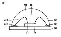
図6は、半導体発光素子10の使用形態の一例を示す側面図である。図6では、半導体発光素子10を簡略化している。図7および図8においても同様である。半導体発光素子10は、セラミック基板610上に設けられている。セラミック基板610は第1の電極611と第2の電極613とを有し、第1の電極611は導電性細線615を介して半導体発光素子10のn側電極20に接続され、第2の電極613は導電性細線617を介して半導体発光素子10のp側電極21に接続されている。
Claims (5)
- 基板と、
前記基板上に設けられ、少なくとも第1導電型半導体層と発光層と第2導電型半導体層とを有する半導体積層部と
を備えた半導体発光素子であって、
前記基板は、
前記発光層からの光に対して透光性を有し、
前記半導体積層部が設けられる第1の面と、前記第1の面とは反対側に位置する第2の面と、前記第1の面および前記第2の面に直交する一対の第3の面と、前記第1の面および前記第2の面に直交し、前記一対の第3の面とは異なる一対の第4の面とを含む六面体形状を有し、
前記第1の面は、凹部と凸部とが交互に形成されてなる凹凸構造を有し、
前記第3の面は、それぞれ、前記第2の面から第1の距離離れた位置に第1の改質層を有し、
前記第4の面は、それぞれ、2以上の改質層を有する半導体発光素子。 - 前記第1の面では、前記発光層からの光が前記第3の面に平行な方向には前記凸部で遮られることなく伝播する一方前記第3の面とは垂直な方向には前記凸部で遮られるように、前記凹部と前記凸部とが形成されている請求項1に記載の半導体発光素子。
- 前記基板は、結晶構造を有する材料からなり、
前記第3の面は、前記基板の<1-100>方向に平行であり、
前記第4の面は、前記基板の<11-20>方向に平行である請求項2に記載の半導体発光素子。 - 前記第1の改質層の厚さは、0μmより大きく、
前記2以上の改質層の厚さは、それぞれ、0μmより大きく、
前記第1の改質層よりも前記第1の面側に位置する基板の部分の厚さは、30μm以上であり、
前記2以上の改質層のうち最も前記第1の面側に位置する改質層よりも前記第1の面側に位置する基板の部分の厚さは、30μm以上である請求項1~3のいずれかに記載の半導体発光素子。 - 前記第1の改質層は、前記基板の厚さ方向とは垂直な方向に延びており、
前記2以上の改質層は、それぞれ、前記基板の厚さ方向とは垂直な方向に延びている請求項1~4のいずれかに記載の半導体発光素子。
Priority Applications (4)
| Application Number | Priority Date | Filing Date | Title |
|---|---|---|---|
| US14/653,813 US9466763B2 (en) | 2013-09-03 | 2014-06-10 | Semiconductor light-emitting element |
| JP2014561645A JPWO2015033638A1 (ja) | 2013-09-03 | 2014-06-10 | 半導体発光素子 |
| CN201480002009.4A CN104620398B (zh) | 2013-09-03 | 2014-06-10 | 半导体发光元件 |
| US15/253,330 US9818911B2 (en) | 2013-09-03 | 2016-08-31 | Semiconductor light-emitting element |
Applications Claiming Priority (2)
| Application Number | Priority Date | Filing Date | Title |
|---|---|---|---|
| JP2013182039 | 2013-09-03 | ||
| JP2013-182039 | 2013-09-03 |
Related Child Applications (2)
| Application Number | Title | Priority Date | Filing Date |
|---|---|---|---|
| US14/653,813 A-371-Of-International US9466763B2 (en) | 2013-09-03 | 2014-06-10 | Semiconductor light-emitting element |
| US15/253,330 Continuation US9818911B2 (en) | 2013-09-03 | 2016-08-31 | Semiconductor light-emitting element |
Publications (1)
| Publication Number | Publication Date |
|---|---|
| WO2015033638A1 true WO2015033638A1 (ja) | 2015-03-12 |
Family
ID=52628128
Family Applications (1)
| Application Number | Title | Priority Date | Filing Date |
|---|---|---|---|
| PCT/JP2014/065322 Ceased WO2015033638A1 (ja) | 2013-09-03 | 2014-06-10 | 半導体発光素子 |
Country Status (4)
| Country | Link |
|---|---|
| US (2) | US9466763B2 (ja) |
| JP (1) | JPWO2015033638A1 (ja) |
| CN (1) | CN104620398B (ja) |
| WO (1) | WO2015033638A1 (ja) |
Cited By (2)
| Publication number | Priority date | Publication date | Assignee | Title |
|---|---|---|---|---|
| JP2024015304A (ja) * | 2019-12-06 | 2024-02-01 | ローム株式会社 | SiC半導体装置 |
| US12471339B2 (en) | 2018-08-10 | 2025-11-11 | Rohm Co., Ltd. | SiC semiconductor device |
Families Citing this family (9)
| Publication number | Priority date | Publication date | Assignee | Title |
|---|---|---|---|---|
| CN104620398B (zh) * | 2013-09-03 | 2017-05-03 | 夏普株式会社 | 半导体发光元件 |
| JP5553292B1 (ja) * | 2013-12-03 | 2014-07-16 | エルシード株式会社 | Led素子 |
| TW201523917A (zh) * | 2013-12-12 | 2015-06-16 | Hwasun Quartek Corp | 磊晶基板、其製造方法及發光二極體 |
| JP6375890B2 (ja) * | 2014-11-18 | 2018-08-22 | 日亜化学工業株式会社 | 窒化物半導体素子及びその製造方法 |
| TWI568016B (zh) * | 2014-12-23 | 2017-01-21 | 錼創科技股份有限公司 | 半導體發光元件 |
| US9873170B2 (en) * | 2015-03-24 | 2018-01-23 | Nichia Corporation | Method of manufacturing light emitting element |
| CN105336837A (zh) * | 2015-09-29 | 2016-02-17 | 佛山市国星光电股份有限公司 | 一种led器件及其制作方法 |
| TWI786248B (zh) * | 2018-12-26 | 2022-12-11 | 晶元光電股份有限公司 | 發光元件 |
| CN113192883A (zh) * | 2021-04-20 | 2021-07-30 | 天津三安光电有限公司 | 红外发光二极管及其制备方法 |
Citations (4)
| Publication number | Priority date | Publication date | Assignee | Title |
|---|---|---|---|---|
| WO2011090024A1 (ja) * | 2010-01-19 | 2011-07-28 | シャープ株式会社 | 機能素子およびその製造方法 |
| JP2012079720A (ja) * | 2010-09-30 | 2012-04-19 | Toyoda Gosei Co Ltd | Iii族窒化物半導体発光素子の製造方法 |
| JP2013021250A (ja) * | 2011-07-14 | 2013-01-31 | Toshiba Corp | 半導体発光素子 |
| JP2013051260A (ja) * | 2011-08-30 | 2013-03-14 | Toyoda Gosei Co Ltd | 半導体発光チップの製造方法および半導体発光チップ |
Family Cites Families (16)
| Publication number | Priority date | Publication date | Assignee | Title |
|---|---|---|---|---|
| TW253999B (ja) * | 1993-06-30 | 1995-08-11 | Hitachi Cable | |
| JP2007165850A (ja) * | 2005-11-16 | 2007-06-28 | Denso Corp | ウェハおよびウェハの分断方法 |
| US20080258165A1 (en) * | 2007-04-23 | 2008-10-23 | Goldeneye, Inc. | Light emitting diode chip |
| US8575633B2 (en) * | 2008-12-08 | 2013-11-05 | Cree, Inc. | Light emitting diode with improved light extraction |
| KR100993088B1 (ko) * | 2008-07-22 | 2010-11-08 | 엘지이노텍 주식회사 | 반도체 발광소자 및 그 제조방법 |
| KR101123010B1 (ko) | 2008-12-09 | 2012-06-15 | 삼성엘이디 주식회사 | 반도체 발광소자 및 그 제조방법 |
| JP2012000636A (ja) * | 2010-06-16 | 2012-01-05 | Showa Denko Kk | レーザ加工方法 |
| US8765509B2 (en) * | 2010-09-30 | 2014-07-01 | Toyoda Gosei Co., Ltd. | Method for producing group III nitride semiconductor light-emitting device |
| US8343788B2 (en) * | 2011-04-19 | 2013-01-01 | Epistar Corporation | Light emitting device and manufacturing method thereof |
| KR101259483B1 (ko) * | 2011-06-01 | 2013-05-06 | 서울옵토디바이스주식회사 | 반도체 발광 소자 및 그 제조 방법 |
| CN103999245A (zh) * | 2011-12-14 | 2014-08-20 | 首尔伟傲世有限公司 | 半导体装置及制造半导体装置的方法 |
| KR101894025B1 (ko) * | 2011-12-16 | 2018-09-03 | 엘지이노텍 주식회사 | 발광소자 |
| CN104160520A (zh) * | 2012-02-01 | 2014-11-19 | 松下电器产业株式会社 | 半导体发光元件、其制造方法和光源装置 |
| US9214353B2 (en) * | 2012-02-26 | 2015-12-15 | Solexel, Inc. | Systems and methods for laser splitting and device layer transfer |
| CN104620398B (zh) * | 2013-09-03 | 2017-05-03 | 夏普株式会社 | 半导体发光元件 |
| TWI614914B (zh) * | 2014-07-11 | 2018-02-11 | 晶元光電股份有限公司 | 發光元件及其製造方法 |
-
2014
- 2014-06-10 CN CN201480002009.4A patent/CN104620398B/zh active Active
- 2014-06-10 JP JP2014561645A patent/JPWO2015033638A1/ja active Pending
- 2014-06-10 WO PCT/JP2014/065322 patent/WO2015033638A1/ja not_active Ceased
- 2014-06-10 US US14/653,813 patent/US9466763B2/en active Active
-
2016
- 2016-08-31 US US15/253,330 patent/US9818911B2/en active Active
Patent Citations (4)
| Publication number | Priority date | Publication date | Assignee | Title |
|---|---|---|---|---|
| WO2011090024A1 (ja) * | 2010-01-19 | 2011-07-28 | シャープ株式会社 | 機能素子およびその製造方法 |
| JP2012079720A (ja) * | 2010-09-30 | 2012-04-19 | Toyoda Gosei Co Ltd | Iii族窒化物半導体発光素子の製造方法 |
| JP2013021250A (ja) * | 2011-07-14 | 2013-01-31 | Toshiba Corp | 半導体発光素子 |
| JP2013051260A (ja) * | 2011-08-30 | 2013-03-14 | Toyoda Gosei Co Ltd | 半導体発光チップの製造方法および半導体発光チップ |
Cited By (3)
| Publication number | Priority date | Publication date | Assignee | Title |
|---|---|---|---|---|
| US12471339B2 (en) | 2018-08-10 | 2025-11-11 | Rohm Co., Ltd. | SiC semiconductor device |
| JP2024015304A (ja) * | 2019-12-06 | 2024-02-01 | ローム株式会社 | SiC半導体装置 |
| JP7661459B2 (ja) | 2019-12-06 | 2025-04-14 | ローム株式会社 | SiC半導体装置 |
Also Published As
| Publication number | Publication date |
|---|---|
| CN104620398A (zh) | 2015-05-13 |
| CN104620398B (zh) | 2017-05-03 |
| US9466763B2 (en) | 2016-10-11 |
| US20150349202A1 (en) | 2015-12-03 |
| US20160372632A1 (en) | 2016-12-22 |
| JPWO2015033638A1 (ja) | 2017-03-02 |
| US9818911B2 (en) | 2017-11-14 |
Similar Documents
| Publication | Publication Date | Title |
|---|---|---|
| WO2015033638A1 (ja) | 半導体発光素子 | |
| KR101451036B1 (ko) | 반도체 발광 소자 | |
| TWI513065B (zh) | Semiconductor light emitting device and light emitting device | |
| TWI514631B (zh) | Semiconductor light emitting device and manufacturing method thereof | |
| JP6419077B2 (ja) | 波長変換発光デバイス | |
| KR101548066B1 (ko) | 발광 장치, 발광 모듈, 및 발광 장치의 제조 방법 | |
| CN101432900B (zh) | 带有支承衬底的发射辐射的半导体本体及其制造方法 | |
| JP5276680B2 (ja) | 発光素子パッケージ、照明システム | |
| US20170294553A1 (en) | Manufacturing method of light-emitting device | |
| JP5531575B2 (ja) | Iii族窒化物化合物半導体発光素子 | |
| TWI493758B (zh) | 半導體發光裝置及發光模組 | |
| TW201342660A (zh) | 半導體發光裝置及其製造方法 | |
| TW201434181A (zh) | 半導體發光裝置及其製造方法 | |
| TW201637241A (zh) | 半導體發光元件、發光裝置及半導體發光元件之製造方法 | |
| KR20230026248A (ko) | 발광소자 | |
| KR102464320B1 (ko) | 발광 소자 패키지 | |
| JP2005197573A (ja) | Iii族窒化物半導体発光素子 | |
| KR101499954B1 (ko) | 수직구조 그룹 3족 질화물계 반도체 발광다이오드 소자 및제조방법 | |
| JP6067400B2 (ja) | 半導体発光素子 | |
| JP4947569B2 (ja) | 半導体発光素子及びその製造方法 | |
| KR102307081B1 (ko) | 성형된 기판을 갖는 반도체 발광 디바이스 및 그 제조 방법 | |
| JP6259286B2 (ja) | 窒化物半導体発光素子 | |
| KR101499953B1 (ko) | 수직구조 그룹 3족 질화물계 반도체 발광다이오드 소자 및제조방법 | |
| JP7227476B2 (ja) | 発光装置及びその製造方法 | |
| KR101337613B1 (ko) | 발광소자와 그 제조방법 |
Legal Events
| Date | Code | Title | Description |
|---|---|---|---|
| ENP | Entry into the national phase |
Ref document number: 2014561645 Country of ref document: JP Kind code of ref document: A |
|
| 121 | Ep: the epo has been informed by wipo that ep was designated in this application |
Ref document number: 14842524 Country of ref document: EP Kind code of ref document: A1 |
|
| WWE | Wipo information: entry into national phase |
Ref document number: 14653813 Country of ref document: US |
|
| NENP | Non-entry into the national phase |
Ref country code: DE |
|
| 122 | Ep: pct application non-entry in european phase |
Ref document number: 14842524 Country of ref document: EP Kind code of ref document: A1 |