WO2015016149A1 - 基板処理装置、半導体装置の製造方法および記録媒体 - Google Patents
基板処理装置、半導体装置の製造方法および記録媒体 Download PDFInfo
- Publication number
- WO2015016149A1 WO2015016149A1 PCT/JP2014/069701 JP2014069701W WO2015016149A1 WO 2015016149 A1 WO2015016149 A1 WO 2015016149A1 JP 2014069701 W JP2014069701 W JP 2014069701W WO 2015016149 A1 WO2015016149 A1 WO 2015016149A1
- Authority
- WO
- WIPO (PCT)
- Prior art keywords
- gas
- substrate
- film
- modified layer
- processing
- Prior art date
Links
- 239000000758 substrate Substances 0.000 title claims abstract description 137
- 238000004519 manufacturing process Methods 0.000 title claims abstract description 36
- 239000004065 semiconductor Substances 0.000 title claims abstract description 36
- 239000003795 chemical substances by application Substances 0.000 claims abstract description 48
- 229910052736 halogen Inorganic materials 0.000 claims abstract description 28
- 150000002367 halogens Chemical class 0.000 claims abstract description 27
- 239000007789 gas Substances 0.000 claims description 197
- 238000000034 method Methods 0.000 claims description 68
- XRURPHMPXJDCOO-UHFFFAOYSA-N iodine heptafluoride Chemical compound FI(F)(F)(F)(F)(F)F XRURPHMPXJDCOO-UHFFFAOYSA-N 0.000 claims description 22
- VYPSYNLAJGMNEJ-UHFFFAOYSA-N Silicium dioxide Chemical group O=[Si]=O VYPSYNLAJGMNEJ-UHFFFAOYSA-N 0.000 claims description 15
- 229910052814 silicon oxide Inorganic materials 0.000 claims description 13
- 229910052581 Si3N4 Inorganic materials 0.000 claims description 7
- HQVNEWCFYHHQES-UHFFFAOYSA-N silicon nitride Chemical group N12[Si]34N5[Si]62N3[Si]51N64 HQVNEWCFYHHQES-UHFFFAOYSA-N 0.000 claims description 7
- BLIQUJLAJXRXSG-UHFFFAOYSA-N 1-benzyl-3-(trifluoromethyl)pyrrolidin-1-ium-3-carboxylate Chemical compound C1C(C(=O)O)(C(F)(F)F)CCN1CC1=CC=CC=C1 BLIQUJLAJXRXSG-UHFFFAOYSA-N 0.000 claims description 5
- TVVNZBSLUREFJN-UHFFFAOYSA-N 2-(4-chlorophenyl)sulfanyl-5-nitrobenzaldehyde Chemical compound O=CC1=CC([N+](=O)[O-])=CC=C1SC1=CC=C(Cl)C=C1 TVVNZBSLUREFJN-UHFFFAOYSA-N 0.000 claims description 5
- CEBDXRXVGUQZJK-UHFFFAOYSA-N 2-methyl-1-benzofuran-7-carboxylic acid Chemical compound C1=CC(C(O)=O)=C2OC(C)=CC2=C1 CEBDXRXVGUQZJK-UHFFFAOYSA-N 0.000 claims description 5
- FQFKTKUFHWNTBN-UHFFFAOYSA-N trifluoro-$l^{3}-bromane Chemical compound FBr(F)F FQFKTKUFHWNTBN-UHFFFAOYSA-N 0.000 claims description 5
- ZCYVEMRRCGMTRW-UHFFFAOYSA-N 7553-56-2 Chemical compound [I] ZCYVEMRRCGMTRW-UHFFFAOYSA-N 0.000 claims description 4
- PXGOKWXKJXAPGV-UHFFFAOYSA-N Fluorine Chemical compound FF PXGOKWXKJXAPGV-UHFFFAOYSA-N 0.000 claims description 4
- UFHFLCQGNIYNRP-UHFFFAOYSA-N Hydrogen Chemical compound [H][H] UFHFLCQGNIYNRP-UHFFFAOYSA-N 0.000 claims description 4
- 229910052731 fluorine Inorganic materials 0.000 claims description 4
- 239000011737 fluorine Substances 0.000 claims description 4
- 229910052740 iodine Inorganic materials 0.000 claims description 4
- 239000011630 iodine Substances 0.000 claims description 4
- JOHWNGGYGAVMGU-UHFFFAOYSA-N trifluorochlorine Chemical compound FCl(F)F JOHWNGGYGAVMGU-UHFFFAOYSA-N 0.000 claims description 4
- 230000003213 activating effect Effects 0.000 claims description 3
- XUIMIQQOPSSXEZ-UHFFFAOYSA-N Silicon Chemical compound [Si] XUIMIQQOPSSXEZ-UHFFFAOYSA-N 0.000 description 72
- 229910052710 silicon Inorganic materials 0.000 description 72
- 239000010703 silicon Substances 0.000 description 72
- 235000012431 wafers Nutrition 0.000 description 56
- 230000008569 process Effects 0.000 description 36
- 239000011261 inert gas Substances 0.000 description 20
- 238000006243 chemical reaction Methods 0.000 description 17
- 238000003860 storage Methods 0.000 description 16
- 238000005530 etching Methods 0.000 description 15
- 238000010926 purge Methods 0.000 description 12
- 238000010790 dilution Methods 0.000 description 8
- 239000012895 dilution Substances 0.000 description 8
- 238000010438 heat treatment Methods 0.000 description 8
- 230000007246 mechanism Effects 0.000 description 8
- 238000002156 mixing Methods 0.000 description 7
- XKRFYHLGVUSROY-UHFFFAOYSA-N Argon Chemical compound [Ar] XKRFYHLGVUSROY-UHFFFAOYSA-N 0.000 description 6
- QVGXLLKOCUKJST-UHFFFAOYSA-N atomic oxygen Chemical compound [O] QVGXLLKOCUKJST-UHFFFAOYSA-N 0.000 description 6
- 238000004140 cleaning Methods 0.000 description 6
- 230000005284 excitation Effects 0.000 description 6
- 150000004767 nitrides Chemical class 0.000 description 6
- 239000001301 oxygen Substances 0.000 description 6
- 229910052760 oxygen Inorganic materials 0.000 description 6
- IJGRMHOSHXDMSA-UHFFFAOYSA-N Atomic nitrogen Chemical compound N#N IJGRMHOSHXDMSA-UHFFFAOYSA-N 0.000 description 5
- 238000001816 cooling Methods 0.000 description 5
- 150000002431 hydrogen Chemical class 0.000 description 5
- RYGMFSIKBFXOCR-UHFFFAOYSA-N Copper Chemical compound [Cu] RYGMFSIKBFXOCR-UHFFFAOYSA-N 0.000 description 4
- 230000008859 change Effects 0.000 description 4
- 229910052802 copper Inorganic materials 0.000 description 4
- 239000010949 copper Substances 0.000 description 4
- 238000001312 dry etching Methods 0.000 description 4
- 239000007788 liquid Substances 0.000 description 4
- 229910052751 metal Inorganic materials 0.000 description 4
- 239000002184 metal Substances 0.000 description 4
- 238000004544 sputter deposition Methods 0.000 description 4
- 230000001629 suppression Effects 0.000 description 4
- 238000001039 wet etching Methods 0.000 description 4
- NRTOMJZYCJJWKI-UHFFFAOYSA-N Titanium nitride Chemical compound [Ti]#N NRTOMJZYCJJWKI-UHFFFAOYSA-N 0.000 description 3
- 229910052782 aluminium Inorganic materials 0.000 description 3
- XAGFODPZIPBFFR-UHFFFAOYSA-N aluminium Chemical compound [Al] XAGFODPZIPBFFR-UHFFFAOYSA-N 0.000 description 3
- 229910052786 argon Inorganic materials 0.000 description 3
- 238000004891 communication Methods 0.000 description 3
- 238000010586 diagram Methods 0.000 description 3
- 230000006870 function Effects 0.000 description 3
- 239000001257 hydrogen Substances 0.000 description 3
- 229910052739 hydrogen Inorganic materials 0.000 description 3
- 239000012528 membrane Substances 0.000 description 3
- 230000003647 oxidation Effects 0.000 description 3
- 238000007254 oxidation reaction Methods 0.000 description 3
- 238000000059 patterning Methods 0.000 description 3
- 238000001179 sorption measurement Methods 0.000 description 3
- KZBUYRJDOAKODT-UHFFFAOYSA-N Chlorine Chemical compound ClCl KZBUYRJDOAKODT-UHFFFAOYSA-N 0.000 description 2
- 229910021417 amorphous silicon Inorganic materials 0.000 description 2
- 239000000919 ceramic Substances 0.000 description 2
- 239000000460 chlorine Substances 0.000 description 2
- 238000001514 detection method Methods 0.000 description 2
- 230000000694 effects Effects 0.000 description 2
- 238000011068 loading method Methods 0.000 description 2
- 239000000463 material Substances 0.000 description 2
- 239000007769 metal material Substances 0.000 description 2
- 229910021420 polycrystalline silicon Inorganic materials 0.000 description 2
- 229920005591 polysilicon Polymers 0.000 description 2
- 238000004804 winding Methods 0.000 description 2
- ZQXCQTAELHSNAT-UHFFFAOYSA-N 1-chloro-3-nitro-5-(trifluoromethyl)benzene Chemical compound [O-][N+](=O)C1=CC(Cl)=CC(C(F)(F)F)=C1 ZQXCQTAELHSNAT-UHFFFAOYSA-N 0.000 description 1
- 229910000838 Al alloy Inorganic materials 0.000 description 1
- WKBOTKDWSSQWDR-UHFFFAOYSA-N Bromine atom Chemical compound [Br] WKBOTKDWSSQWDR-UHFFFAOYSA-N 0.000 description 1
- OKTJSMMVPCPJKN-UHFFFAOYSA-N Carbon Chemical compound [C] OKTJSMMVPCPJKN-UHFFFAOYSA-N 0.000 description 1
- 229910000881 Cu alloy Inorganic materials 0.000 description 1
- KRHYYFGTRYWZRS-UHFFFAOYSA-N Fluorane Chemical compound F KRHYYFGTRYWZRS-UHFFFAOYSA-N 0.000 description 1
- 229910004298 SiO 2 Inorganic materials 0.000 description 1
- 229910003481 amorphous carbon Inorganic materials 0.000 description 1
- 239000007864 aqueous solution Substances 0.000 description 1
- 238000004380 ashing Methods 0.000 description 1
- 238000000429 assembly Methods 0.000 description 1
- 230000000712 assembly Effects 0.000 description 1
- 238000005452 bending Methods 0.000 description 1
- 230000005540 biological transmission Effects 0.000 description 1
- 230000015572 biosynthetic process Effects 0.000 description 1
- GDTBXPJZTBHREO-UHFFFAOYSA-N bromine Substances BrBr GDTBXPJZTBHREO-UHFFFAOYSA-N 0.000 description 1
- 229910052794 bromium Inorganic materials 0.000 description 1
- 229910052799 carbon Inorganic materials 0.000 description 1
- 239000007795 chemical reaction product Substances 0.000 description 1
- 229910052801 chlorine Inorganic materials 0.000 description 1
- 239000004020 conductor Substances 0.000 description 1
- 230000006866 deterioration Effects 0.000 description 1
- 238000001035 drying Methods 0.000 description 1
- 238000005516 engineering process Methods 0.000 description 1
- 238000001704 evaporation Methods 0.000 description 1
- 239000011521 glass Substances 0.000 description 1
- 230000005484 gravity Effects 0.000 description 1
- -1 halogen salt Chemical class 0.000 description 1
- 229910000040 hydrogen fluoride Inorganic materials 0.000 description 1
- 230000006872 improvement Effects 0.000 description 1
- 238000009434 installation Methods 0.000 description 1
- 239000011810 insulating material Substances 0.000 description 1
- 239000004973 liquid crystal related substance Substances 0.000 description 1
- 239000000203 mixture Substances 0.000 description 1
- 229910021421 monocrystalline silicon Inorganic materials 0.000 description 1
- 229910052757 nitrogen Inorganic materials 0.000 description 1
- 230000003287 optical effect Effects 0.000 description 1
- 230000001590 oxidative effect Effects 0.000 description 1
- 230000035515 penetration Effects 0.000 description 1
- 230000002093 peripheral effect Effects 0.000 description 1
- 239000012466 permeate Substances 0.000 description 1
- 238000009832 plasma treatment Methods 0.000 description 1
- 229920000642 polymer Polymers 0.000 description 1
- 238000002360 preparation method Methods 0.000 description 1
- 230000002265 prevention Effects 0.000 description 1
- 238000003672 processing method Methods 0.000 description 1
- 230000009257 reactivity Effects 0.000 description 1
- 230000004044 response Effects 0.000 description 1
- 239000000126 substance Substances 0.000 description 1
- 238000009966 trimming Methods 0.000 description 1
- 238000009834 vaporization Methods 0.000 description 1
- 230000008016 vaporization Effects 0.000 description 1
- 238000009423 ventilation Methods 0.000 description 1
- XLYOFNOQVPJJNP-UHFFFAOYSA-N water Substances O XLYOFNOQVPJJNP-UHFFFAOYSA-N 0.000 description 1
Images


Classifications
-
- H—ELECTRICITY
- H01—ELECTRIC ELEMENTS
- H01L—SEMICONDUCTOR DEVICES NOT COVERED BY CLASS H10
- H01L21/00—Processes or apparatus adapted for the manufacture or treatment of semiconductor or solid state devices or of parts thereof
- H01L21/02—Manufacture or treatment of semiconductor devices or of parts thereof
- H01L21/02041—Cleaning
- H01L21/02057—Cleaning during device manufacture
- H01L21/02068—Cleaning during device manufacture during, before or after processing of conductive layers, e.g. polysilicon or amorphous silicon layers
-
- H—ELECTRICITY
- H01—ELECTRIC ELEMENTS
- H01J—ELECTRIC DISCHARGE TUBES OR DISCHARGE LAMPS
- H01J37/00—Discharge tubes with provision for introducing objects or material to be exposed to the discharge, e.g. for the purpose of examination or processing thereof
- H01J37/32—Gas-filled discharge tubes
- H01J37/32009—Arrangements for generation of plasma specially adapted for examination or treatment of objects, e.g. plasma sources
- H01J37/32082—Radio frequency generated discharge
- H01J37/321—Radio frequency generated discharge the radio frequency energy being inductively coupled to the plasma
-
- H—ELECTRICITY
- H01—ELECTRIC ELEMENTS
- H01L—SEMICONDUCTOR DEVICES NOT COVERED BY CLASS H10
- H01L21/00—Processes or apparatus adapted for the manufacture or treatment of semiconductor or solid state devices or of parts thereof
- H01L21/02—Manufacture or treatment of semiconductor devices or of parts thereof
- H01L21/04—Manufacture or treatment of semiconductor devices or of parts thereof the devices having potential barriers, e.g. a PN junction, depletion layer or carrier concentration layer
- H01L21/18—Manufacture or treatment of semiconductor devices or of parts thereof the devices having potential barriers, e.g. a PN junction, depletion layer or carrier concentration layer the devices having semiconductor bodies comprising elements of Group IV of the Periodic Table or AIIIBV compounds with or without impurities, e.g. doping materials
- H01L21/30—Treatment of semiconductor bodies using processes or apparatus not provided for in groups H01L21/20 - H01L21/26
- H01L21/302—Treatment of semiconductor bodies using processes or apparatus not provided for in groups H01L21/20 - H01L21/26 to change their surface-physical characteristics or shape, e.g. etching, polishing, cutting
- H01L21/306—Chemical or electrical treatment, e.g. electrolytic etching
- H01L21/3065—Plasma etching; Reactive-ion etching
-
- H—ELECTRICITY
- H01—ELECTRIC ELEMENTS
- H01L—SEMICONDUCTOR DEVICES NOT COVERED BY CLASS H10
- H01L21/00—Processes or apparatus adapted for the manufacture or treatment of semiconductor or solid state devices or of parts thereof
- H01L21/02—Manufacture or treatment of semiconductor devices or of parts thereof
- H01L21/04—Manufacture or treatment of semiconductor devices or of parts thereof the devices having potential barriers, e.g. a PN junction, depletion layer or carrier concentration layer
- H01L21/18—Manufacture or treatment of semiconductor devices or of parts thereof the devices having potential barriers, e.g. a PN junction, depletion layer or carrier concentration layer the devices having semiconductor bodies comprising elements of Group IV of the Periodic Table or AIIIBV compounds with or without impurities, e.g. doping materials
- H01L21/30—Treatment of semiconductor bodies using processes or apparatus not provided for in groups H01L21/20 - H01L21/26
- H01L21/31—Treatment of semiconductor bodies using processes or apparatus not provided for in groups H01L21/20 - H01L21/26 to form insulating layers thereon, e.g. for masking or by using photolithographic techniques; After treatment of these layers; Selection of materials for these layers
- H01L21/3105—After-treatment
- H01L21/311—Etching the insulating layers by chemical or physical means
- H01L21/31105—Etching inorganic layers
- H01L21/31111—Etching inorganic layers by chemical means
- H01L21/31116—Etching inorganic layers by chemical means by dry-etching
-
- H—ELECTRICITY
- H01—ELECTRIC ELEMENTS
- H01L—SEMICONDUCTOR DEVICES NOT COVERED BY CLASS H10
- H01L21/00—Processes or apparatus adapted for the manufacture or treatment of semiconductor or solid state devices or of parts thereof
- H01L21/02—Manufacture or treatment of semiconductor devices or of parts thereof
- H01L21/04—Manufacture or treatment of semiconductor devices or of parts thereof the devices having potential barriers, e.g. a PN junction, depletion layer or carrier concentration layer
- H01L21/18—Manufacture or treatment of semiconductor devices or of parts thereof the devices having potential barriers, e.g. a PN junction, depletion layer or carrier concentration layer the devices having semiconductor bodies comprising elements of Group IV of the Periodic Table or AIIIBV compounds with or without impurities, e.g. doping materials
- H01L21/30—Treatment of semiconductor bodies using processes or apparatus not provided for in groups H01L21/20 - H01L21/26
- H01L21/31—Treatment of semiconductor bodies using processes or apparatus not provided for in groups H01L21/20 - H01L21/26 to form insulating layers thereon, e.g. for masking or by using photolithographic techniques; After treatment of these layers; Selection of materials for these layers
- H01L21/3205—Deposition of non-insulating-, e.g. conductive- or resistive-, layers on insulating layers; After-treatment of these layers
- H01L21/321—After treatment
- H01L21/3213—Physical or chemical etching of the layers, e.g. to produce a patterned layer from a pre-deposited extensive layer
- H01L21/32133—Physical or chemical etching of the layers, e.g. to produce a patterned layer from a pre-deposited extensive layer by chemical means only
- H01L21/32135—Physical or chemical etching of the layers, e.g. to produce a patterned layer from a pre-deposited extensive layer by chemical means only by vapour etching only
- H01L21/32138—Physical or chemical etching of the layers, e.g. to produce a patterned layer from a pre-deposited extensive layer by chemical means only by vapour etching only pre- or post-treatments, e.g. anti-corrosion processes
-
- H—ELECTRICITY
- H01—ELECTRIC ELEMENTS
- H01L—SEMICONDUCTOR DEVICES NOT COVERED BY CLASS H10
- H01L21/00—Processes or apparatus adapted for the manufacture or treatment of semiconductor or solid state devices or of parts thereof
- H01L21/67—Apparatus specially adapted for handling semiconductor or electric solid state devices during manufacture or treatment thereof; Apparatus specially adapted for handling wafers during manufacture or treatment of semiconductor or electric solid state devices or components ; Apparatus not specifically provided for elsewhere
- H01L21/67005—Apparatus not specifically provided for elsewhere
- H01L21/67011—Apparatus for manufacture or treatment
- H01L21/67017—Apparatus for fluid treatment
- H01L21/67063—Apparatus for fluid treatment for etching
- H01L21/67069—Apparatus for fluid treatment for etching for drying etching
-
- H—ELECTRICITY
- H01—ELECTRIC ELEMENTS
- H01L—SEMICONDUCTOR DEVICES NOT COVERED BY CLASS H10
- H01L21/00—Processes or apparatus adapted for the manufacture or treatment of semiconductor or solid state devices or of parts thereof
- H01L21/67—Apparatus specially adapted for handling semiconductor or electric solid state devices during manufacture or treatment thereof; Apparatus specially adapted for handling wafers during manufacture or treatment of semiconductor or electric solid state devices or components ; Apparatus not specifically provided for elsewhere
- H01L21/67005—Apparatus not specifically provided for elsewhere
- H01L21/67011—Apparatus for manufacture or treatment
- H01L21/67155—Apparatus for manufacturing or treating in a plurality of work-stations
- H01L21/67207—Apparatus for manufacturing or treating in a plurality of work-stations comprising a chamber adapted to a particular process
-
- H—ELECTRICITY
- H01—ELECTRIC ELEMENTS
- H01L—SEMICONDUCTOR DEVICES NOT COVERED BY CLASS H10
- H01L21/00—Processes or apparatus adapted for the manufacture or treatment of semiconductor or solid state devices or of parts thereof
- H01L21/67—Apparatus specially adapted for handling semiconductor or electric solid state devices during manufacture or treatment thereof; Apparatus specially adapted for handling wafers during manufacture or treatment of semiconductor or electric solid state devices or components ; Apparatus not specifically provided for elsewhere
- H01L21/677—Apparatus specially adapted for handling semiconductor or electric solid state devices during manufacture or treatment thereof; Apparatus specially adapted for handling wafers during manufacture or treatment of semiconductor or electric solid state devices or components ; Apparatus not specifically provided for elsewhere for conveying, e.g. between different workstations
- H01L21/67739—Apparatus specially adapted for handling semiconductor or electric solid state devices during manufacture or treatment thereof; Apparatus specially adapted for handling wafers during manufacture or treatment of semiconductor or electric solid state devices or components ; Apparatus not specifically provided for elsewhere for conveying, e.g. between different workstations into and out of processing chamber
- H01L21/67745—Apparatus specially adapted for handling semiconductor or electric solid state devices during manufacture or treatment thereof; Apparatus specially adapted for handling wafers during manufacture or treatment of semiconductor or electric solid state devices or components ; Apparatus not specifically provided for elsewhere for conveying, e.g. between different workstations into and out of processing chamber characterized by movements or sequence of movements of transfer devices
-
- H—ELECTRICITY
- H01—ELECTRIC ELEMENTS
- H01L—SEMICONDUCTOR DEVICES NOT COVERED BY CLASS H10
- H01L21/00—Processes or apparatus adapted for the manufacture or treatment of semiconductor or solid state devices or of parts thereof
- H01L21/67—Apparatus specially adapted for handling semiconductor or electric solid state devices during manufacture or treatment thereof; Apparatus specially adapted for handling wafers during manufacture or treatment of semiconductor or electric solid state devices or components ; Apparatus not specifically provided for elsewhere
- H01L21/67005—Apparatus not specifically provided for elsewhere
- H01L21/67011—Apparatus for manufacture or treatment
- H01L21/67098—Apparatus for thermal treatment
- H01L21/67109—Apparatus for thermal treatment mainly by convection
Definitions
- the present invention relates to a substrate processing apparatus for processing a substrate, a method for manufacturing a semiconductor device, and a recording medium.
- LSIs Large Scale Integrated Circuits
- patterning technology is also being miniaturized.
- chemical wet etching is mainly used. For example, it is described in Patent Document 1.
- the minimum processing dimensions of semiconductor devices represented by recent LSIs, DRAMs (Dynamic Random Access Memory) and Flash Memory are smaller than 30 nm.
- wet etching which is one step in the manufacturing process of such a semiconductor device, the following problems occur. For example, the pattern collapses due to the surface tension of the liquid used during wet etching. It has become difficult to achieve miniaturization and improvement in manufacturing throughput while maintaining the quality of semiconductor devices.
- a removing agent is supplied to a substrate having a modified layer formed on a Si-containing film, the modified layer removing step of removing the modified layer, and a processing gas containing two or more halogen elements on the substrate. And a film removal step of removing the Si-containing film.
- a processing container that houses a substrate having a modified layer formed on a Si-containing film, a modified layer removing step that supplies the substrate to the substrate, and a film that supplies the processing gas to the substrate
- a substrate processing apparatus having a removal step, and a control unit that controls the removal agent supply unit and the processing gas supply unit.
- a removal agent is supplied to a substrate on which a modified layer is formed on a Si-containing film, and the modified layer removing procedure for removing the modified layer, and a treatment including two or more halogen elements on the substrate.
- a recording medium in which a program for causing a computer to execute a film removal procedure for supplying gas and removing the Si-containing film is provided.
- the manufacturing quality of the semiconductor device can be improved and the manufacturing throughput can be improved.
- the inventors have performed dry etching using a processing gas, which will be described later, so that at least silicon oxide (SiO 2), silicon nitride (Si 3 N 4), titanium nitride (TiN), amorphous carbon (a For -C), it has been found that a Si-containing film containing Si element as a main component can be selectively removed. It has been found that by using a processing gas described later, the Si-containing film can be isotropically removed without converting the processing gas into plasma.
- the Si-containing film is, for example, a film containing 90% or more of Si element.
- FIG. 1 is a schematic configuration diagram of a substrate processing apparatus according to the present embodiment, and shows a processing furnace 202 portion in a longitudinal section.
- a silicon nitride film 601 as a stopper film, a titanium nitride film 602 as a cylindrical electrode, and silicon as a collapse-preventing support part for the electrode are provided on the wafer 600 as a substrate.
- a modified layer 605 a is formed on the nitride film 603, the silicon-containing film 604, and the silicon-containing film 604.
- the silicon-containing film 604 is a mold silicon film for forming the electrode, and is removed in a silicon-containing film removing process described later. Examples of the mold silicon film include amorphous silicon, polysilicon, doped silicon, and single crystal silicon.
- the denatured layer 605a is, for example, a silicon oxide film formed by adsorbing or diffusing oxygen on the surface or upper part of the mold silicon film.
- FIG. 2B illustrates a case where a denatured layer (interface denatured layer 605b) formed by oxidizing the silicon-containing film 604 is present at the interface between the silicon-containing film 604 and the titanium nitride film 602. is doing. In this case, the interface modified layer 605b remains after the silicon-containing film 604 is removed. As described above, there may be an interface modified layer 605b remaining after the removal of the mold silicon-containing film. As another example, FIG.
- FIG. 2C shows a silicon hard mask 607 as a film to be removed, a denatured layer 605a, an SOC (Spin On Carbon) film 606 as a buried film, and a silicon nitride film as a stopper film covering the silicon substrate surface.
- a film (or silicon oxide film) 601 is formed.
- the silicon hard mask 607 includes, for example, amorphous silicon, polysilicon, doped silicon, or the like.
- the surface of the silicon hard mask 607 is modified in the natural oxidation of the surface of the silicon hard mask 607, the dry etching process for patterning the silicon hard mask 607, or the removal process of the resist film. It is assumed that a modified layer 605a on the surface is generated.
- the inventor performs selective substrate processing for removing a silicon-containing film by combining a modified layer removing step described later and a silicon-containing film removing step on the substrate as shown in FIGS. I found.
- the processing vessel 431 is usually formed in a cylindrical shape from a non-metallic material such as quartz glass or ceramics. However, a metal material may be used if there is no particular inconvenience.
- the upper end of the processing vessel 431 is closed by a top plate 454, the lower end is closed by a horizontal base plate 448 as a gantry and a bottom substrate 469, and is hermetically sealed by a pressure adjusting mechanism described later.
- the upper space in the processing container 431 is a gas mixing chamber 430.
- the gas mixing chamber 430 is optimized according to a desired gas flow and mixing state. Further, a shower plate may be provided in the gas mixing chamber 430 so that the gas is directly supplied to the processing chamber 445 described later.
- a space below the base plate 448 and in which the wafer 600 is provided is a processing chamber 445. Further, when the silicon oxide film is removed using plasma, plasma is generated in the plasma mixing chamber 430 and in a space facing a resonance coil 432 as an excitation unit described later.
- a susceptor 459 is provided on the bottom surface of the processing chamber 445.
- the susceptor 459 includes a susceptor table 411 and a substrate heating unit 463 that maintains the wafer on the susceptor at a predetermined temperature.
- the substrate heating unit 463 may include a cooling mechanism for removing excessive heat as necessary.
- the susceptor 459 has a structure supported by a plurality of support columns 461.
- a plurality of lifter pins 413 are provided through the susceptor table 411, and wafer support pins 414 are provided above the lifter pins 413. Wafer support pins 414 extend toward the center of the susceptor 459.
- Wafer 600 is placed on susceptor table 411 or wafer support pins 414.
- the wafer support pins 414 are configured to support the outer periphery of the wafer 600, but may be configured to support the vicinity of the center of the wafer 600 as necessary. By supporting the vicinity of the center of the substrate, it is possible to reduce the bending of the substrate that occurs when a large-diameter substrate having a substrate diameter of 450 mm is supported, and to improve the processing uniformity. For example, when the substrate is bent, the gas flow near the bent portion and the wafer temperature are different from the flow and temperature other than the bent portion, and the processing uniformity may change.
- the substrate support portion is composed of wafer support pins 414. In some cases, the susceptor table 411 and the lifter pin 413 may be considered.
- the lifter pin 413 is connected to the lift board 471 and can be moved up and down by the lift drive unit 490 along the guide shaft 467.
- An exhaust part is provided below the susceptor 459.
- the exhaust part has an APC (Auto Pressure Control) valve 479 and an exhaust pipe 480 as pressure adjusting parts (pressure adjusting mechanisms).
- the exhaust pump 481 may be included in the exhaust section.
- the valve opening degree of the APC valve 479 is configured to be feedback controlled based on the pressure in the processing chamber 445.
- the pressure in the processing chamber 445 is measured by a pressure sensor (not shown).
- the halogen-containing gas used in the present embodiment is heavier than nitrogen (N2) gas, which is a general purge gas.
- iodine heptafluoride (IF7) gas which will be described later, has a specific gravity at room temperature of about 2.7 and is about 2.8 times heavier than nitrogen (N2) gas. For this reason, providing an exhaust port at the bottom of the processing chamber where the halogen-containing gas tends to stay is useful for suppressing residual halogen-containing gas.
- IF7 gas iodine heptafluoride (IF7) gas
- N2 nitrogen
- a cylindrical baffle ring 458 and an exhaust plate 465 may be provided in order to improve the flow of the processing gas.
- the baffle ring 458 is uniformly provided with a large number of ventilation holes on the side surface of the cylinder, and the exhaust plate 465 is provided with an exhaust communication hole 475 at the center.
- the first exhaust chamber 474 is formed by the susceptor 459, the baffle ring 458, and the exhaust plate 465, and the second exhaust chamber 476 is formed by the exhaust plate 465 and the bottom substrate 469.
- the second exhaust chamber 476 is communicated with an exhaust communication hole 475.
- An exhaust pipe 480 is communicated with the second exhaust chamber 476.
- a gas supply pipe 455 for supplying a plurality of required processing gases from a gas supply facility (not shown) is attached to the gas inlet 433 on the top plate 454 at the top of the processing vessel 431.
- the gas supply pipe 455 includes a processing gas supply unit that supplies a halogen element-containing gas as a processing gas to the substrate, a removal agent supply unit that supplies a removing agent to the substrate, and other gases, here N2 gas for purging
- a third supply unit (not shown) for supplying cleaning chlorine fluoride (ClF 3) gas or the like is provided as necessary.
- the removing agent for example, hydrogen fluoride gas or the like is used as the removing agent.
- gas is supplied as the removing agent
- the present invention is not limited thereto, and it may be configured to be removable by an etching method by supplying a liquid.
- a rare gas such as argon may be flowed.
- the gas supply units are provided with mass flow controllers 477 and 483 and on-off valves 478 and 484 as flow rate control units, respectively, and can control the gas supply amount.
- mass flow controllers 477 and 483 and on-off valves 478 and 484 as flow rate control units, respectively, and can control the gas supply amount.
- the removal agent supply unit is described here, there may be a third or later gas supply unit.
- the gas to be used may be mixed in advance and then flowed to the gas inlet 433.
- a baffle plate 460 made of quartz glass or ceramics is provided in the processing container 431 to adjust the flow of the processing gas. Moreover, you may make it the structure which uses a shower plate as needed. By adjusting the supply amount and the exhaust amount by the amount control unit and the APC valve 479, the pressures in the processing container 431 and the processing chamber 445 are controlled to desired values.
- an excitation unit for generating plasma When removing the modified layer film using plasma, an excitation unit for generating plasma may be provided. Since the resonance coil 432 as the excitation unit forms a standing wave of a predetermined wavelength, the winding diameter, the winding pitch, and the number of turns are set so as to resonate in a constant wavelength mode. That is, the electrical length of the resonance coil 432 corresponds to an integral multiple (1 times, 2 times,...), Half wavelength, or 1 ⁇ 4 wavelength of one wavelength at a predetermined frequency of power supplied from the high frequency power supply 444. Set to the length to be. For example, in the case of 27.12 MHz, the length of one wavelength is about 11 meters.
- the frequency to be used and the resonance coil length are preferably selected according to the desired plasma generation state, the mechanical dimensions of the plasma generation chamber 430, and the like.
- the resonance coil 432 takes into account the applied power, the generated magnetic field strength, or the external shape of the device to be applied, for example, 0.01 to 10 by high frequency power of 800 kHz to 50 MHz and 0.5 to 5 kW.
- the effective cross-sectional area is 50 to 300 mm 2 and the coil diameter is 200 to 500 mm.
- the coil is wound about 2 to 60 times on the outer peripheral side of the processing vessel 431.
- a material constituting the resonance coil 432 a copper pipe, a copper thin plate, an aluminum pipe, an aluminum thin plate, a material obtained by evaporating a copper plate or aluminum on a polymer belt, or the like is used.
- the resonant coil 432 is formed of an insulating material in a flat plate shape, and is supported by a plurality of support portions that are vertically provided on the upper end surface of the base plate 448.
- Both ends of the resonance coil 432 are electrically grounded, but at least one end of the resonance coil 432 finely adjusts the electrical length of the resonance coil during the initial installation of the apparatus or when processing conditions are changed. Therefore, it is grounded through the operation tap 462. For example, it is grounded by the fixed ground point 464. Further, in order to finely adjust the impedance of the resonance coil 432 when the apparatus is first installed or when the processing conditions are changed, a power feeding unit is configured by a movable tap 466 between the grounded ends of the resonance coil 432. Is done.
- the resonance coil 432 includes ground portions that are electrically grounded at both ends, and includes a power feeding portion that is supplied with power from the high-frequency power source 444 between the ground portions. Further, at least one of the ground portions may be a variable ground portion whose position is adjustable, and the power feeding portion may be a variable power feeding portion whose position is adjustable.
- the resonance coil 432 includes a variable ground portion and a variable power supply portion, the resonance frequency and load impedance of the plasma generation chamber 430 can be adjusted more easily as will be described later. .
- a waveform adjustment circuit including a coil and a shield may be inserted at one end (or both ends) of the resonance coil 432 so that the phase and anti-phase currents flow to the target with respect to the electrical midpoint of the resonance coil 432.
- a waveform adjusting circuit is configured as an open circuit by setting the end of the resonance coil 432 to an electrically disconnected state or an electrically equivalent state.
- the end of the resonance coil 432 may be ungrounded by a choke series resistor and may be DC-connected to a fixed reference voltage.
- the outer shield 452 is provided to shield leakage of electromagnetic waves to the outside of the resonance coil 432 and to form a capacitance component necessary for configuring a resonance circuit with the resonance coil 432.
- the outer shield 452 is generally formed in a cylindrical shape using a conductive material such as aluminum alloy, copper, or copper alloy.
- the outer shield 452 is arranged at a distance of, for example, about 5 to 10 mm from the outer periphery of the resonance coil 432.
- the outer shield 452 is grounded so that the potential is equal to both ends of the resonance coil 432.
- To accurately set the resonance number of the resonance coil 432 one end or both ends of the outer shield 452 are tapped positions.
- the trimming capacitance may be inserted between the resonance coil 432 and the outer shield 452.
- the outer shield 452 and the resonance coil that are electrically grounded constitute a spiral resonator.
- an appropriate power source such as an RF generator can be used as long as it is a power source that can supply power of a necessary voltage and frequency to the resonance coil 432.
- a high frequency power source capable of supplying power of about 0.5 to 5 kW at a frequency of 80 kHz to 800 MHz is used.
- a reflected wave power meter 468 is installed on the output side of the high frequency power supply 444, and the reflected wave power detected by the reflected wave power meter 468 is input to the controller 500 used as a control unit.
- the controller 470 does not simply control only the high-frequency power supply 444 but controls the entire substrate processing apparatus including, for example, the operation of the substrate transfer mechanism and the gate valve.
- a display 472 as a display device displays data detected by various detection units provided in the substrate processing apparatus such as a detection result of a reflected wave by the reflected wave wattmeter 468, for example.
- the high frequency power supply 444 is provided with a frequency matching unit 446 that controls the transmission frequency.
- the excitation unit is constituted by the resonance coil 432, but may include one or more of the high frequency power supply 444, the external shield 452, the reflected wave wattmeter 468, and the frequency matching unit 446.
- the transport system for transporting the substrate includes an EFEM (Equipment Front End Module) 100, a load lock chamber unit 200, and a transfer module unit 300.
- EFEM Equipment Front End Module
- the EFEM 100 includes FOUPs (Front Opening Unified Pods) 110 and 120 and an atmospheric transfer robot 130 which is a first transfer unit that transfers wafers from the respective FOUPs to the load lock chamber. 25 wafers are mounted on the FOUP, and the arm unit of the atmospheric transfer robot 130 pulls out the wafers from the FOUP five by five.
- the inside of the EFEM 100 and the inside of the FOUPs 110 and 120 may be made an inert gas atmosphere in order to suppress the natural oxidation of the wafer as necessary.
- the load lock chamber unit 200 includes load lock chambers 250 and 260 and buffer units 210 and 220 for holding the wafer 600 transferred from the FOUP in the load lock chambers 250 and 260, respectively.
- the buffer units 210 and 220 include boats 211 and 221 and index assemblies 212 and 222 below them.
- the boat 211 (221) and the index assembly 212 (222) below the boat 211 (221) rotate simultaneously by the ⁇ axis 214 (224).
- the load lock chamber 200 may be in a vacuum atmosphere, an inert gas atmosphere, or a decompressed atmosphere to which an inert gas is supplied.
- the transfer module unit 300 includes a transfer module 310 used as a transfer chamber, and the above-described load lock chambers 250 and 260 are attached to the transfer module 310 via gate valves 311 and 312.
- the transfer module 310 is provided with a vacuum arm robot unit 320 used as a second transfer unit.
- the inside of the transfer module unit 300 may be a vacuum atmosphere, an inert gas atmosphere, or a reduced pressure atmosphere to which an inert gas is supplied.
- the inside of the load lock chamber unit 200 and the transfer module unit 300 is set to a reduced pressure atmosphere to which an inert gas is supplied. It is preferable.
- the process chamber section 400 includes processing chambers 410 and 420, and gas mixing chambers 430 and 440 provided on the processing chambers 410 and 420, respectively.
- the processing chambers 410 and 420 are attached to the transfer module 310 via gate valves 313 and 314.
- the processing chamber 420 has the same configuration as 410.
- the controller 500 controls the above-described units so as to perform a substrate processing process described later.
- the controller 500 which is a control unit (control means), is configured as a computer including a CPU (Central Processing Unit) 500a, a RAM (Random Access Memory) 500b, a storage device 500c, and an I / O port 500d.
- the RAM 500b, the storage device 500c, and the I / O port 500d are configured to exchange data with the CPU 500a via the internal bus 500e.
- an input / output device 501 configured as a touch panel or the like is connected to the controller 500.
- the storage device 500c includes, for example, a flash memory, a HDD (Hard Disk Drive), and the like.
- a control program that controls the operation of the substrate processing apparatus, a process recipe that describes the procedure and conditions of the substrate processing described later, and the like are stored in a readable manner.
- the process recipe is a combination of functions so that a predetermined result can be obtained by causing the controller 500 to execute each procedure in a substrate processing step to be described later, and functions as a program.
- the process recipe, the control program, and the like are collectively referred to as simply a program.
- the RAM 500b is configured as a memory area (work area) in which programs, data, and the like read by the CPU 500a are temporarily stored.
- the I / O port 500d includes the above-described lift drive unit 490, substrate temperature adjustment unit 463, APC valve 479, mass flow controllers 477 and 483, on-off valves 478 and 484, exhaust pump 481, atmospheric transfer robot 130, gate valve 313, and the like. 314, connected to the vacuum arm robot unit 320 and the like.
- the high frequency power supply 444, the movable tap 466, the reflected power meter 468, and the frequency matching unit 446 are configured to be connectable.
- the CPU 500a is configured to read and execute a control program from the storage device 500c, and to read a process recipe from the storage device 500c in response to an operation command input from the input / output device 501. Then, the CPU 500a moves the lifter pin 413 up and down by the lift drive unit 490, the heating / cooling operation of the wafer 600 by the substrate temperature adjustment unit 463, the pressure adjustment operation by the APC valve 479, in accordance with the contents of the read process recipe.
- the flow rate adjusting operation of the processing gas by the mass flow controllers 477 and 483 and the on-off valves 478 and 484 is controlled.
- the controller 500 is not limited to being configured as a dedicated computer, but may be configured as a general-purpose computer.
- an external storage device for example, a magnetic tape, a magnetic disk such as a flexible disk or a hard disk, an optical disk such as a CD or a DVD, a magneto-optical disk such as an MO, a USB memory (USB Flash Drive) or a memory card that stores the above-described program.
- the controller 500 according to the present embodiment can be configured by preparing a semiconductor memory) 123 and installing a program in a general-purpose computer using the external storage device 123.
- the means for supplying the program to the computer is not limited to supplying the program via the external storage device 123.
- the program may be supplied without using the external storage device 123 by using communication means such as the Internet or a dedicated line.
- the storage device 500c and the external storage device 123 are configured as computer-readable recording media. Hereinafter, these are collectively referred to simply as a recording medium. Note that when the term “recording medium” is used in this specification, it may include only the storage device 500c alone, may include only the external storage device 123 alone, or may include both.
- the wafer 600 is transferred from the FOUP 110 to the load lock chamber 250 by the atmospheric transfer robot 130.
- evacuation is performed, and the atmosphere or inert gas atmosphere in the EFEM is replaced with a vacuum atmosphere, an inert gas atmosphere, or a decompressed atmosphere to which an inert gas is supplied.
- the gate valve 311 between the load lock chamber 250 and the transfer module 310 is opened, and the wafer 600 is transferred from the load lock chamber 250 into the transfer module 310 by the vacuum arm robot unit 320. .
- the gate valve 311 is closed.
- the wafer is mounted on the wafer support pins 414 on the lifter pins 413 through the gate valve 313 provided between the transfer module 310 and the plasma processing unit 410.
- the gate valve 313 is closed.
- the transfer path is purged with an inert gas and the pressure is reduced.
- the lifter pins 413 are lowered, and the wafer 600 is placed on the susceptor table 411.
- the lifter pin 413 is lifted and lowered by the lift drive unit 490.
- the substrate temperature adjustment unit 463 provided in the susceptor 459 is heated to a predetermined temperature in advance, and heats the wafer 600 to a predetermined wafer temperature from room temperature to low temperature. If necessary, a cooling mechanism for exhausting excess heat (reaction heat) is also used.
- the low temperature is a temperature range in which a removal gas and a processing gas described later are sufficiently vaporized, and is a temperature at which the film characteristics formed on the wafer 600 do not change.
- a removal gas as a predetermined removal agent is supplied from the gas supply pipe 445 to the wafer 600, and the denatured layer is removed from the wafer 600.
- the denatured layer is removed by supplying a removing agent to the wafer 600.
- the removal gas is supplied.
- HF gas is used as the removal gas
- a predetermined gas flow rate is set in a range of 0.1 slm to 10 slm. For example, it is set to 3 slm.
- the pressure in the processing chamber is, for example, 1 Pa to 1300 Pa.
- a predetermined pressure is set. For example, it is set to 100 Pa.
- HF gas is particularly effective for removing the silicon oxide film, but can also be used for removing the silicon nitride film.
- HF gas may be introduced into the processing chamber, or a mixed gas of IF7 gas and hydrogen (H2) gas may be introduced into the processing chamber and converted into plasma to generate an HF gas component.
- H2 gas a mixed gas of IF7 gas and hydrogen (H2) gas
- IF7 gas a preliminary process of a Si-containing film removal process described later can be performed. That is, the intermediate layer between the modified layer and the silicon-containing film can be removed, and the silicon-containing film can be more reliably removed in the silicon-containing film removal step.
- H2 hydrogen
- a reducing gas may be supplied to remove oxygen.
- An example of the reducing gas is hydrogen (H 2) gas.
- H 2 gas hydrogen
- the modified layer may be removed by a wet etching method using a removing liquid (for example, HF aqueous solution) as a removing agent.
- the denatured layer is obtained by supplying a wafer 600 using a gas obtained by activating (plasmaizing) one or both of a rare gas such as argon (Ar) and a reducing gas such as hydrogen gas as a removing agent. May be removed.
- a rare gas such as argon (Ar)
- a reducing gas such as hydrogen gas as a removing agent. May be removed.
- the denatured layer can be reduced by supplying activated hydrogen to the wafer 600.
- activated remover for example, activated Ar
- the denatured layer 605a can be obtained without damaging the SOC film 606 as a buried film as compared with the case of using HF gas. Can be removed. That is, the denatured layer 605a can be removed without impairing the function as the embedded film.
- Modified layer suppression step S40 In this step, after the modified layer is removed, the modified layer is prevented from growing again. For example, the generation of the modified layer is suppressed by keeping the wafer 600 in an inert gas atmosphere, a reducing atmosphere, or a vacuum atmosphere. In this embodiment, since a series of processing is performed in the same processing chamber, it is possible to quickly move to the next step without mixing oxygen in the atmosphere of the processing chamber.
- a predetermined processing gas is supplied from the gas supply pipe 445.
- the processing gas supplies a halogen-containing gas, an inert gas for purging or dilution, or the like as an etching gas.
- the halogen-containing gas is, for example, a gas containing two or more halogen elements from fluorine (F), chlorine (Cl), bromine (Br), and iodine (I).
- IF7 iodine pentafluoride
- IF7 bromine trifluoride
- BrF3 bromine pentafluoride
- XeF2 xenon difluoride
- ClF3 chlorine trifluoride
- IF7 is used.
- the IF 7 can positively (selectively) remove the silicon-containing film.
- “selectively” means, for example, that the etching rate of the silicon-containing film is made higher than the etching rate of other films (for example, metal films).
- nitrogen (N 2) gas is used as the inert gas, but it may be a rare gas such as He, Ne, or Ar.
- the total pressure in the processing chamber 445 is within a range of about 1 to 1330 Pa, and the partial pressure of the IF 7 is within a range of about 1 to 1330 Pa.
- Maintain the pressure of. For example, it is maintained at 100 Pa.
- Each gas flow rate is set to a predetermined flow rate within a range of about 0.1 to 10 SLM. For example, it is set to 3 SLM.
- a predetermined gas may be supplied after the atmosphere of the processing container 431 and the processing chamber 445 is once exhausted. Further, since the etching of the silicon-containing film is started as soon as the IF7 gas is supplied, it is desirable that the pressure and the gas flow rate are quickly set to predetermined values.
- reaction heat is generated by the contact between the processing gas and the silicon film. It is considered that the reaction heat is conducted to the metal film or the substrate by heat conduction, and as a result, the characteristic deterioration of the metal film or the warpage of the substrate occurs. Furthermore, it is conceivable that the temperature of the wafer 600 is out of a predetermined temperature range and the high selectivity of the processing gas is lost.
- the concentration of the processing gas and the etching rate are in a proportional relationship, and the etching rate and the amount of reaction heat are in a proportional relationship, when the etching rate is increased by increasing the concentration of the processing gas, the metal due to the above reaction heat Heating of the film and the substrate becomes remarkable.
- the processing gas concentration is reduced, and an excessive temperature rise due to reaction heat is suppressed.
- the supply amount of the dilution gas is set larger than the supply amount of the processing gas.
- the dilution gas may be supplied simultaneously with the processing gas, or the processing gas may be supplied after the dilution gas is supplied.
- the processing gas By supplying the processing gas later in this way, it is possible to prevent a processing gas having a high concentration from being supplied to the wafer 600 and improve the processing uniformity of the wafer 600. In addition, a rapid temperature change of the wafer 600 due to reaction heat can be suppressed.
- the dilution gas is supplied, and the processing gas is supplied after the pressure in the processing chamber is stabilized.
- the amount of dilution gas is sufficiently larger than the amount of processing gas, and is effective, for example, in a process for controlling the etching depth. Since etching is performed in a state where the pressure is stable, the etching rate can be stabilized. As a result, the etching depth can be easily controlled.
- Silicon-containing film removal step S60 By maintaining the substrate temperature, pressure, and gas flow rate at predetermined values for a predetermined time, the silicon-containing film is selectively removed by a predetermined amount.
- Modified layer removal step S70 If necessary, the denatured layer remaining after removing the silicon-containing film is removed.
- the denatured layer is removed.
- the removal of the denatured layer is performed, for example, by supplying a removal gas.
- HF gas may be introduced into the processing chamber, or a mixed gas with IF7 gas H2 gas may be introduced into the processing chamber and converted into plasma to generate HF gas components.
- IF7 gas By supplying the IF7 gas, the silicon-containing film can be removed even if the silicon-containing film remains in the above-described silicon-containing film removal step. Further, the intermediate film between the silicon-containing film and the modified layer can also be removed.
- the denatured layer is removed by supplying the wafer 600 using a gas obtained by activating (plasmaizing) one or both of a rare gas such as argon and a reducing gas such as hydrogen gas as a removing agent. May be.
- the modified layer can be removed by sputtering.
- the denatured layer can be reduced by supplying activated hydrogen to the wafer 600.
- the denatured layer 605a can be removed without damaging the SOC film 606 as a buried film.
- Substrate unloading step S90 When the wafer 600 is cooled to a temperature at which the wafer 600 can be transported and is ready to be unloaded from the processing chamber, the wafer 600 is unloaded by the reverse procedure of the substrate loading step S10.
- the fine high aspect ratio structure includes, for example, a pillar structure.
- the fine high aspect ratio structure includes, for example, a pillar structure.
- the wafer 600 on which the fine and high aspect ratio structure is exposed is wet-cleaned, there is a problem that the pattern collapses as described above. Therefore, it is particularly important to remove the denatured layer that becomes a residue base before removing the silicon-containing film.
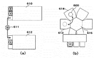
- FIG. 8A illustrates another aspect of the substrate processing flow.
- the silicon-containing film removing step S60 is performed by the silicon-containing film removing device 612.
- production of a new modified layer is suppressed by storing and conveying a board
- the denatured layer film is removed by a wet cleaning apparatus, and the substrate is transferred to an apparatus for removing the silicon-containing film using N2 purge FOUP (Front Opening Unified Pod). Is mentioned.
- N2 purge FOUP Front Opening Unified Pod
- the modified layer removing method is not limited to wet cleaning, and may be a dry process using gas.
- the method for removing the modified layer and the method for suppressing the new modified layer can be variously improved, changed, and added by those skilled in the art within the scope of the technical idea of the present invention.
- FIG. 8B illustrates still another aspect of the substrate processing flow.
- a reaction chamber 613 for removing a denatured layer and a reaction chamber 614 for removing a silicon-containing film are connected by a vacuum transfer chamber 615 purged with an inert gas.
- the case where the process of (2) is performed continuously is illustrated.
- the modified layer removal steps S30 and S70 are performed in the reaction chamber 613
- the modified layer suppression step S40 is performed in the vacuum transfer chamber 615
- the silicon-containing film removal step S60 is performed in the reaction chamber 614.
- the modified layer removal steps S30 and S70 may be performed in separate reaction chambers.
- the silicon-containing film can be removed without collapsing the electrode formed on the substrate by removing the silicon-containing film with a halogen-containing gas after removing the denatured layer with the removal gas.
- the oxide film formed in the interface of a silicon containing film and an electrode can be removed by performing the removal process of a modified layer after a silicon containing film removal process.
- the modified layer can be removed without damaging the embedded film by performing the removal of the modified layer using either or both of the activated rare gas and the activated reducing gas. it can.
- the present invention includes a step of removing a denatured layer existing on the surface of a silicon-containing film to be removed, a step of suppressing the generation of a new denatured layer, and a silicon content to be removed
- the present invention provides a substrate processing method and a substrate processing apparatus capable of selectively removing silicon while removing an unnecessary denatured layer by combining a step of removing a denatured layer present at a location covered with a film.
- the scope of implementation is not limited by the number of simultaneously processed substrates, the direction in which the substrate is held, the type of dilution gas or purge gas, the cleaning method, the shape of the substrate processing chamber, heating mechanism, and cooling mechanism, etc. .
- the process of directly removing the target film using the removal gas or the processing gas is described.
- the present invention is not limited to this, and a reaction product is generated by reacting the halogen salt gas with the silicon oxide film. May be removed by heating and vaporization.
- the silicon oxide film formed on the silicon-containing film is described as the modified layer.
- the present invention is not limited to this.
- a nitride film is formed on the surface of the substrate or a film formed on the substrate.
- this nitride film exists, the same problem as described above may occur, and the amount of remaining nitride film can be suppressed by removing the nitride film (modified layer) before removing the silicon-containing film. it can.
- the denatured layer formed on the mold silicon film for electrode formation is removed with the remover, and the mold silicon film is removed with the processing gas.
- the present invention is not limited to this.
- a natural oxide film formed on the surface of the dummy gate electrode is removed with a remover, and then the dummy gate electrode is removed with a processing gas. May be.
- the present invention is not limited to a semiconductor manufacturing apparatus that processes a semiconductor wafer such as the substrate processing apparatus according to the present embodiment, but an LCD (Liquid Crystal Display) manufacturing apparatus, a solar cell manufacturing apparatus, or the like that processes a glass substrate.
- the present invention can also be applied to a substrate processing apparatus and a MEMS (Micro Electro Mechanical Systems) manufacturing apparatus.
- a processing container containing a substrate having a modified layer formed on a Si-containing film, a modified layer removing step of supplying the removing agent to the modified layer, and the processing gas for the substrate.
- a substrate processing apparatus comprising: a control unit that controls the removal agent supply unit and the processing gas supply unit so as to perform a film removal step of supplying a Si-containing film.
- halogen elements are preferably fluorine and iodine.
- ⁇ Appendix 3> The substrate processing apparatus according to appendix 1 or appendix 2, wherein the processing gas is preferably iodine pentafluoride, iodine heptafluoride, bromine trifluoride, bromine pentafluoride, xenon difluoride, trifluoride. It is a gas in which any one of chlorine chloride or a combination of two or more thereof.
- ⁇ Appendix 6> It is a substrate processing apparatus as described in any one of the supplementary notes 1 thru
- control unit preferably supplies the processing gas after supplying the removing agent in the denatured layer removing step.
- the removal agent supply unit and the processing gas supply unit are controlled.
- ⁇ Appendix 8> The substrate processing apparatus according to any one of appendices 1 to 7, preferably, in the film removal step, the control unit supplies the removal agent after supplying the processing gas.
- the removal agent supply unit and the processing gas supply unit are controlled.
- ⁇ Appendix 9> The substrate processing apparatus according to appendix 7, wherein, preferably, in the modified layer removal step, the control unit and the removal agent supply unit perform the film removal step after stopping the supply of the removal agent. Control the processing gas supply unit.
- control unit preferably includes the removal agent supply unit so as to stop the supply of the processing gas after supplying the removal agent in the film removal step.
- the processing gas supply unit is controlled.
- ⁇ Appendix 11> The substrate processing apparatus according to any one of Supplementary Note 1 to Supplementary Note 10, wherein the processing gas is preferably generated by exciting a mixed gas of a gas containing a halogen element and a basic gas.
- ⁇ Appendix 12> The substrate processing apparatus according to any one of appendices 1 to 11, wherein the removal agent is preferably an activated rare gas.
- ⁇ Appendix 14> The substrate processing apparatus according to any one of Supplementary Note 1 to Supplementary Note 11, wherein the removal agent is preferably an activated reducing gas.
- a step of carrying a substrate on which a modified layer is formed on a Si-containing film into a processing container, a modified layer removing step of supplying a removing agent to the modified layer and removing the modified layer, There is provided a method for manufacturing a semiconductor device, comprising: supplying a processing gas containing two or more halogen elements to the Si-containing film and removing the Si-containing film.
- halogen elements are preferably fluorine and iodine.
- ⁇ Appendix 18> The method for manufacturing a semiconductor device according to appendix 16 or appendix 17, wherein the processing gas is preferably iodine pentafluoride, iodine heptafluoride, bromine trifluoride, bromine pentafluoride, xenon difluoride,
- the gas is a combination of any one or more of chlorine trifluoride.
- ⁇ Appendix 19> 19 The method for manufacturing a semiconductor device according to any one of appendix 16 to appendix 18, wherein the modified layer is preferably a silicon oxide film.
- the substrate processing apparatus according to any one of appendix 16 to appendix 19, preferably, in the modified layer removal step, a step of supplying a removal gas containing a rare gas, and the removal gas being activated. A step.
- ⁇ Appendix 21> The substrate processing apparatus according to any one of appendix 16 to appendix 20, preferably, in the modified layer removal step, a step of supplying a removal gas containing a reducing gas, and the removal gas is activated Steps.
- ⁇ Appendix 22> The substrate processing apparatus according to any one of Supplementary Note 16 to Supplementary Note 21, preferably having a modified layer suppressing step for suppressing generation of a modified layer after the film removing step.
- ⁇ Appendix 24> 24 The method for manufacturing a semiconductor device according to any one of appendix 16 to appendix 23, wherein the processing gas is preferably supplied after the removal agent is supplied in the modified layer removal step.
- ⁇ Appendix 25> 25 The method of manufacturing a semiconductor device according to any one of appendix 16 to appendix 24, wherein, in the film removal step, the removal agent is supplied after supplying the processing gas.
- ⁇ Appendix 26> The method for manufacturing a semiconductor device according to attachment 24, preferably, in the modified layer removing step, the film removing step is performed after the supply of the removing agent is stopped.
- a procedure for carrying a substrate having a modified layer formed on a Si-containing film into a processing container, a modified layer removing procedure for supplying a removing agent to the modified layer and removing the modified layer There is provided a program for causing a computer to execute a film removing procedure for supplying a processing gas containing two or more halogen elements to the Si-containing film and removing the Si-containing film.
- a procedure for carrying a substrate having a modified layer formed on a Si-containing film into a processing container, a modified layer removing procedure for supplying a removing agent to the modified layer and removing the modified layer There is provided a recording medium in which a program for causing a computer to execute a film removing procedure for supplying a processing gas containing two or more halogen elements to the Si-containing film and removing the Si-containing film is provided.
- a substrate having a modified layer formed on a Si-containing film wherein a removing agent is supplied to the modified layer to remove the modified layer, and the Si-containing film And a film removal step of removing the Si-containing film by supplying a processing gas containing two or more halogen elements to the substrate.
- a substrate having a semiconductor device structure in which a modified layer is formed on a Si-containing film, wherein a removing agent is supplied to the modified layer and the modified layer is removed.
- the substrate processing apparatus According to the substrate processing apparatus, the semiconductor device manufacturing method, and the recording medium according to the present invention, it is possible to improve the manufacturing quality of the semiconductor device and the manufacturing throughput.
Landscapes
- Engineering & Computer Science (AREA)
- Physics & Mathematics (AREA)
- Computer Hardware Design (AREA)
- Microelectronics & Electronic Packaging (AREA)
- Power Engineering (AREA)
- Condensed Matter Physics & Semiconductors (AREA)
- General Physics & Mathematics (AREA)
- Manufacturing & Machinery (AREA)
- Chemical & Material Sciences (AREA)
- General Chemical & Material Sciences (AREA)
- Chemical Kinetics & Catalysis (AREA)
- Plasma & Fusion (AREA)
- Analytical Chemistry (AREA)
- Inorganic Chemistry (AREA)
- Drying Of Semiconductors (AREA)
- Plasma Technology (AREA)
Priority Applications (3)
| Application Number | Priority Date | Filing Date | Title |
|---|---|---|---|
| JP2015529550A JPWO2015016149A1 (ja) | 2013-07-29 | 2014-07-25 | 基板処理装置、半導体装置の製造方法およびプログラム |
| KR1020167002323A KR20160025591A (ko) | 2013-07-29 | 2014-07-25 | 기판 처리 장치, 반도체 장치의 제조 방법 및 기록 매체 |
| US15/007,513 US20160155630A1 (en) | 2013-07-29 | 2016-01-27 | Substrate processing apparatus, method for manufacturing semiconductor device, and recording medium |
Applications Claiming Priority (2)
| Application Number | Priority Date | Filing Date | Title |
|---|---|---|---|
| JP2013-156958 | 2013-07-29 | ||
| JP2013156958 | 2013-07-29 |
Related Child Applications (1)
| Application Number | Title | Priority Date | Filing Date |
|---|---|---|---|
| US15/007,513 Continuation US20160155630A1 (en) | 2013-07-29 | 2016-01-27 | Substrate processing apparatus, method for manufacturing semiconductor device, and recording medium |
Publications (1)
| Publication Number | Publication Date |
|---|---|
| WO2015016149A1 true WO2015016149A1 (ja) | 2015-02-05 |
Family
ID=52431684
Family Applications (1)
| Application Number | Title | Priority Date | Filing Date |
|---|---|---|---|
| PCT/JP2014/069701 WO2015016149A1 (ja) | 2013-07-29 | 2014-07-25 | 基板処理装置、半導体装置の製造方法および記録媒体 |
Country Status (5)
| Country | Link |
|---|---|
| US (1) | US20160155630A1 (ko) |
| JP (1) | JPWO2015016149A1 (ko) |
| KR (1) | KR20160025591A (ko) |
| TW (1) | TW201519314A (ko) |
| WO (1) | WO2015016149A1 (ko) |
Cited By (1)
| Publication number | Priority date | Publication date | Assignee | Title |
|---|---|---|---|---|
| WO2020255631A1 (ja) * | 2019-06-18 | 2020-12-24 | 昭和電工株式会社 | プラズマエッチング方法 |
Families Citing this family (7)
| Publication number | Priority date | Publication date | Assignee | Title |
|---|---|---|---|---|
| JP6438831B2 (ja) * | 2015-04-20 | 2018-12-19 | 東京エレクトロン株式会社 | 有機膜をエッチングする方法 |
| JP6434617B2 (ja) * | 2015-05-22 | 2018-12-05 | 株式会社日立ハイテクノロジーズ | プラズマ処理装置およびそれを用いたプラズマ処理方法 |
| JP6817757B2 (ja) * | 2016-09-16 | 2021-01-20 | 東京エレクトロン株式会社 | 基板処理装置及び基板移送方法 |
| JP7002268B2 (ja) * | 2017-09-28 | 2022-01-20 | 東京エレクトロン株式会社 | プラズマ処理装置 |
| JP6981267B2 (ja) * | 2018-01-17 | 2021-12-15 | 東京エレクトロン株式会社 | エッチング方法及びエッチング装置 |
| FR3101196B1 (fr) * | 2019-09-20 | 2021-10-01 | Semco Smartech France | Dispositif d'homogeneisation |
| KR20210081591A (ko) * | 2019-12-24 | 2021-07-02 | (주)에스티아이 | 기판 처리 장치 및 기판 처리 방법 |
Citations (7)
| Publication number | Priority date | Publication date | Assignee | Title |
|---|---|---|---|---|
| JPH06196455A (ja) * | 1991-07-31 | 1994-07-15 | Kawasaki Steel Corp | 半導体基板の処理方法 |
| JPH06204191A (ja) * | 1992-11-10 | 1994-07-22 | Sony Corp | 金属プラグ形成後の表面処理方法 |
| JPH08172079A (ja) * | 1994-10-17 | 1996-07-02 | Semiconductor Energy Lab Co Ltd | 薄膜半導体の作製方法 |
| JPH11214512A (ja) * | 1998-01-20 | 1999-08-06 | Sony Corp | 半導体装置の製造方法 |
| JP2002113700A (ja) * | 2000-10-05 | 2002-04-16 | Sony Corp | マイクロマシン製造装置、マイクロマシンの製造方法、回折格子ライトバルブの製造方法および表示装置の製造方法 |
| JP2004349616A (ja) * | 2003-05-26 | 2004-12-09 | Matsushita Electric Ind Co Ltd | 半導体装置の製造方法および半導体製造装置 |
| JP2010245512A (ja) * | 2009-03-19 | 2010-10-28 | Tokyo Electron Ltd | 基板のエッチング方法及びシステム |
Family Cites Families (9)
| Publication number | Priority date | Publication date | Assignee | Title |
|---|---|---|---|---|
| US5888906A (en) * | 1996-09-16 | 1999-03-30 | Micron Technology, Inc. | Plasmaless dry contact cleaning method using interhalogen compounds |
| JPH11150112A (ja) * | 1997-11-19 | 1999-06-02 | Sony Corp | 半導体製造装置および半導体装置の製造方法 |
| KR100338768B1 (ko) * | 1999-10-25 | 2002-05-30 | 윤종용 | 산화막 제거방법 및 산화막 제거를 위한 반도체 제조 장치 |
| US6372657B1 (en) * | 2000-08-31 | 2002-04-16 | Micron Technology, Inc. | Method for selective etching of oxides |
| JP3985537B2 (ja) * | 2002-01-31 | 2007-10-03 | 富士電機デバイステクノロジー株式会社 | 半導体装置の製造方法 |
| JP4115761B2 (ja) * | 2002-07-05 | 2008-07-09 | アルプス電気株式会社 | アクティブマトリクス基板及びその製造方法並びにそれを用いた表示装置 |
| JP4944228B2 (ja) | 2009-09-16 | 2012-05-30 | 株式会社日立国際電気 | 基板処理方法及び基板処理装置 |
| US9064815B2 (en) * | 2011-03-14 | 2015-06-23 | Applied Materials, Inc. | Methods for etch of metal and metal-oxide films |
| JP6056136B2 (ja) * | 2011-09-07 | 2017-01-11 | セントラル硝子株式会社 | ドライエッチング方法 |
-
2014
- 2014-07-25 WO PCT/JP2014/069701 patent/WO2015016149A1/ja active Application Filing
- 2014-07-25 KR KR1020167002323A patent/KR20160025591A/ko not_active Application Discontinuation
- 2014-07-25 JP JP2015529550A patent/JPWO2015016149A1/ja active Pending
- 2014-07-28 TW TW103125678A patent/TW201519314A/zh unknown
-
2016
- 2016-01-27 US US15/007,513 patent/US20160155630A1/en not_active Abandoned
Patent Citations (7)
| Publication number | Priority date | Publication date | Assignee | Title |
|---|---|---|---|---|
| JPH06196455A (ja) * | 1991-07-31 | 1994-07-15 | Kawasaki Steel Corp | 半導体基板の処理方法 |
| JPH06204191A (ja) * | 1992-11-10 | 1994-07-22 | Sony Corp | 金属プラグ形成後の表面処理方法 |
| JPH08172079A (ja) * | 1994-10-17 | 1996-07-02 | Semiconductor Energy Lab Co Ltd | 薄膜半導体の作製方法 |
| JPH11214512A (ja) * | 1998-01-20 | 1999-08-06 | Sony Corp | 半導体装置の製造方法 |
| JP2002113700A (ja) * | 2000-10-05 | 2002-04-16 | Sony Corp | マイクロマシン製造装置、マイクロマシンの製造方法、回折格子ライトバルブの製造方法および表示装置の製造方法 |
| JP2004349616A (ja) * | 2003-05-26 | 2004-12-09 | Matsushita Electric Ind Co Ltd | 半導体装置の製造方法および半導体製造装置 |
| JP2010245512A (ja) * | 2009-03-19 | 2010-10-28 | Tokyo Electron Ltd | 基板のエッチング方法及びシステム |
Cited By (1)
| Publication number | Priority date | Publication date | Assignee | Title |
|---|---|---|---|---|
| WO2020255631A1 (ja) * | 2019-06-18 | 2020-12-24 | 昭和電工株式会社 | プラズマエッチング方法 |
Also Published As
| Publication number | Publication date |
|---|---|
| TW201519314A (zh) | 2015-05-16 |
| US20160155630A1 (en) | 2016-06-02 |
| JPWO2015016149A1 (ja) | 2017-03-02 |
| KR20160025591A (ko) | 2016-03-08 |
Similar Documents
| Publication | Publication Date | Title |
|---|---|---|
| WO2015016149A1 (ja) | 基板処理装置、半導体装置の製造方法および記録媒体 | |
| WO2015060069A1 (ja) | 微細パターンの形成方法、半導体装置の製造方法、及び基板処理装置並びに記録媒体 | |
| JP6210039B2 (ja) | 付着物の除去方法及びドライエッチング方法 | |
| US20130137274A1 (en) | Substrate processing method | |
| WO2015115002A1 (ja) | 微細パターンの形成方法、半導体装置の製造方法、基板処理装置及び記録媒体 | |
| JP6262333B2 (ja) | 基板処理装置、半導体装置の製造方法及びプログラム | |
| KR102526306B1 (ko) | 반도체 제조 방법 및 플라즈마 처리 장치 | |
| US11557486B2 (en) | Etching method, damage layer removal method, and storage medium | |
| WO2018212045A1 (ja) | 多孔質膜をエッチングする方法 | |
| WO2017022086A1 (ja) | 半導体装置の製造方法、エッチング方法、及び基板処理装置並びに記録媒体 | |
| TWI588297B (zh) | Attachment removal method and dry etching method | |
| JP2011176177A (ja) | 半導体デバイスの製造方法、半導体デバイスおよび基板処理装置 | |
| JP2017157660A (ja) | 半導体装置の製造方法および基板処理装置 | |
| JP6529996B2 (ja) | 基板処理装置、半導体装置の製造方法およびプログラム | |
| JP2016072465A (ja) | 半導体装置の製造方法および基板処理装置 | |
| US10504741B2 (en) | Semiconductor manufacturing method and plasma processing apparatus | |
| JP7294999B2 (ja) | エッチング方法 | |
| WO2015011829A1 (ja) | 基板処理装置及び半導体装置の製造方法 | |
| KR102653253B1 (ko) | 기판 처리 방법 및 기판 처리 장치 | |
| JP2012069657A (ja) | 基板処理方法及び基板処理装置 |
Legal Events
| Date | Code | Title | Description |
|---|---|---|---|
| 121 | Ep: the epo has been informed by wipo that ep was designated in this application |
Ref document number: 14831172 Country of ref document: EP Kind code of ref document: A1 |
|
| ENP | Entry into the national phase |
Ref document number: 2015529550 Country of ref document: JP Kind code of ref document: A |
|
| ENP | Entry into the national phase |
Ref document number: 20167002323 Country of ref document: KR Kind code of ref document: A |
|
| NENP | Non-entry into the national phase |
Ref country code: DE |
|
| 122 | Ep: pct application non-entry in european phase |
Ref document number: 14831172 Country of ref document: EP Kind code of ref document: A1 |