WO2015015905A1 - Dispositif arithmétique logique - Google Patents
Dispositif arithmétique logique Download PDFInfo
- Publication number
- WO2015015905A1 WO2015015905A1 PCT/JP2014/065245 JP2014065245W WO2015015905A1 WO 2015015905 A1 WO2015015905 A1 WO 2015015905A1 JP 2014065245 W JP2014065245 W JP 2014065245W WO 2015015905 A1 WO2015015905 A1 WO 2015015905A1
- Authority
- WO
- WIPO (PCT)
- Prior art keywords
- bit
- output
- unit
- logical operation
- memory device
- Prior art date
Links
Images
Classifications
-
- H—ELECTRICITY
- H03—ELECTRONIC CIRCUITRY
- H03K—PULSE TECHNIQUE
- H03K19/00—Logic circuits, i.e. having at least two inputs acting on one output; Inverting circuits
- H03K19/20—Logic circuits, i.e. having at least two inputs acting on one output; Inverting circuits characterised by logic function, e.g. AND, OR, NOR, NOT circuits
- H03K19/21—EXCLUSIVE-OR circuits, i.e. giving output if input signal exists at only one input; COINCIDENCE circuits, i.e. giving output only if all input signals are identical
-
- G—PHYSICS
- G06—COMPUTING; CALCULATING OR COUNTING
- G06F—ELECTRIC DIGITAL DATA PROCESSING
- G06F1/00—Details not covered by groups G06F3/00 - G06F13/00 and G06F21/00
- G06F1/02—Digital function generators
Definitions
- the present invention relates to a logical operation device that performs a logical operation between bits included in an input bit string.
- an exclusive OR operation device for multi-bit length data is configured by combining two-input exclusive OR circuits.
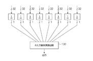
- FIG. 11 shows an example of a logical operation device that calculates an exclusive OR of 32 bits.
- the logical operation device that calculates the 32-bit exclusive OR includes four 8-input exclusive OR circuits 100 and three 2-input exclusive OR circuits 200. .
- the 8-input exclusive OR circuit 100 includes seven 2-input exclusive OR circuits 200 therein.
- Non-Patent Document 1 An example of a multi-input (3-input) exclusive OR gate is disclosed in Non-Patent Document 1.
- the present invention has been made in view of the above circumstances, and provides a logical operation device capable of performing arithmetic processing in a relatively short time with a relatively small circuit configuration even for multi-bit data. This is one of its purposes.
- the present invention for solving the problems of the above conventional example is a logical operation device, which accepts an input of a bit string having a bit length of N (N is an integer of N ⁇ 2) and represents the input bit string
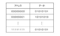
- a memory device for storing a lookup table formed by storing, in an address, multi-bit data including a bit representing a logical operation result between bits included in the input bit string, and the memory device; And an output means for outputting a bit included in data stored at an address represented by the received bit string.
- arithmetic processing can be performed in a relatively short time with a relatively small circuit configuration.
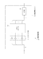
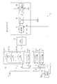
- the logical operation device 1 includes at least one logical operation unit 10 as illustrated in FIG.
- the logical operation unit 10 basically includes an input buffer unit 11, a memory device 12, and an output unit 13.
- the input buffer unit 11 accepts an input of a bit string having a bit length of N (N is an integer of N ⁇ 2) and supplies a signal represented by the bit string to the address bus of the memory device 12. That is, in this example, N corresponds to the address bus width of the memory device 12.
- the memory device 12 is a semiconductor memory such as a nonvolatile memory or an SRAM (Static Random Access Memory), and includes memory cells of 2 N bits ⁇ L bits (L is an integer of L ⁇ 2).
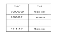
- Data “0XXXXXX” (here, X may be indefinite) including “0”, which is the sum operation result, is stored.
- the address represented by the bit string “00000001” includes data “1XXXXXXXX” (X is indefinite) that includes “1”, which is the operation result of the exclusive OR of the bit string “00000001”, in the MSB (most significant bit). Good) is stored.
- the output unit 13 reads the data stored in the address represented by the bit string output from the input buffer unit 11 among the data stored in the memory device 12.
- the output unit 13 selectively outputs a bit including the logical operation result in the read data.
- the output unit 13 since the logical operation result is included in the MSB, the output unit 13 stores the data stored in the memory device at the address represented by the bit string output by the input buffer unit 11. The read data is read, and the MSB bit of the data is output.
- the memory device 12 includes a bit representing a logical operation result between each bit included in the input bit string at an address represented by the bit string input from the input buffer unit 11.
- a look-up table is stored which stores multi-bit length data including the inverted bit as a part thereof.
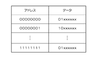
- Data “01XXXXXX” (here, X may be indefinite) including “0” that is the sum operation result and “1” that is the inverted bit of this operation result is stored in the next bit.
- the address represented by the bit string “00000001” includes “1” that is the result of the exclusive OR of the bit string “00000001” in its MSB (most significant bit), and the next bit is the inverted bit.
- Data “10XXXXXXX” (“X” may be indefinite) including “0” is stored.
- the output unit 13 accepts a 1-bit signal input from the outside.
- the output unit 13 reads the data stored in the address represented by the bit string output from the input buffer unit 11 among the data stored in the memory device 12, and the 1-bit signal input from the outside is “0”. "1” or "1”, the logical operation result or its inverted bit is selectively output from the data.
- the output unit 13 is a bit string output from the input buffer unit 11 among the data stored in the memory device when the 1-bit signal input from the outside is “0”. The data stored at the address indicated by is read, and the MSB bit of the data is output.
- the output unit 13 is stored in the address represented by the bit string output from the input buffer unit 11 among the data stored in the memory device.
- the data is read, and the next bit of the MSB of the data (the bit storing the inverted bit of the logical operation result) is output.
- This embodiment basically has the above configuration and operates as in the following example.
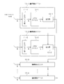
- a plurality of logical operation units 10_1, 10_2,... 10_n are provided as illustrated in FIG.
- the output unit 13_i of the i-th logic operation unit 10_i accepts the output bit of the i-1th logic operation unit 10_i-1 as an input from the outside.
- the output unit 13_1 of the first logical operation unit 10_1 does not receive an external input (or fixes the external input to “0”, for example), and stores the data stored in the memory device 12. Of these, a bit representing the logical operation result (MSB in the above example) is output.
- the output unit 13_1 of the logical operation unit 10_1 is stored in the address represented by the 8-bit long bit string (b1, b2,..., B8) input to the input buffer 11_1 among the data stored in the memory device 12_1. Read data. Then, the bits of the logical operation result (here, the operation result of the exclusive OR of the input 8-bit length bit string) included in the read data are output.
- the output unit 13_2 of the next logical operation unit 10_2 is stored at the address represented by the 8-bit long bit string (b9, b10,..., B16) input to the input buffer 11_2 among the data stored in the memory device 12_2.
- Read out data The output unit 13_2 selects and outputs either the bit of the logical operation result included in the read data or its inverted bit based on the bit output from the output unit 13_1 of the preceding logical operation unit 10_1. To do. Specifically, the output unit 13_2 outputs a logical operation result included in the read data when the bit output from the output unit 13_1 is “0”.
- the output unit 13_2 outputs an inverted bit of the logical operation result when the bit output from the output unit 13_1 is “1”.
- the output unit 13_i of the i-th logical operation unit 10_i uses the 8-bit length bit string (b8 (i-1) +1, b8) input to the input buffer 11_i among the data stored in the memory device 12_i. Read the data stored at the address indicated by (i-1) +2,..., b8i). Further, the output unit 13_i outputs either the bit of the logical operation result included in the read data or its inverted bit based on the bit output from the output unit 13_i-1 of the preceding logical operation unit 10_i-1. Select and output. Specifically, the output unit 13_i outputs a logical operation result included in the read data when the bit output from the output unit 13_i-1 is “0”. The output unit 13_i outputs an inverted bit of the logical operation result when the bit output from the output unit 13_i-1 is “1”.
- the output unit 13_n of the n-th logical operation unit 10_n includes an 8-bit length bit string (b8 (n-1) +1, b8 () input to the input buffer 11_n among the data stored in the memory device 12_n. n-1) +2,... b8n) reads data stored at the address indicated.
- the output unit 13_n outputs either the bit of the logical operation result included in the read data or its inverted bit based on the bit output from the output unit 13_n-1 of the preceding logical operation unit 10_n-1. Select and output. Specifically, the output unit 13_n outputs a logical operation result included in the read data when the bit output from the output unit 13_n ⁇ 1 is “0”.
- the output unit 13_n outputs an inverted bit of the logical operation result when the bit output from the output unit 13_n-1 is “1”.
- the output unit 13_n of the nth logical operation unit 10_n outputs a logical operation result (exclusive OR in this example) of each bit included in the data D having a length of 8 ⁇ n bits.
- the present embodiment is not limited to this.
- the memory device 12 may be used in a time division manner.
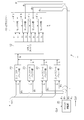
- the logical operation device 1 according to the embodiment of the present invention relating to this example includes n three-state buffer units 20, a memory device 12, a clock supply unit 25, and an output unit 30. It is comprised including.
- Including components having the same configurations as those already described are denoted by the same reference numerals and description thereof is omitted.
- the memory device 12 stores the data illustrated in FIG.
- the three-state buffer 21 includes an input terminal X, an output terminal Y, and a gate terminal G, respectively.
- the three-state buffer 21 sets the state of the output terminal Y to the high impedance state “Z” regardless of what is input to the input terminal X while the input of the gate terminal G is “0”.
- the three-state buffer 21 in which the output terminal Y has a high impedance is the same as an insulated state (a state in which the connection is disconnected).
- 8n three-state buffers 21 are a group from the first three-state buffer 21_1 to the eighth three-state buffer 21_8, and from the ninth three-state buffer 21_9 to the sixteenth.
- the groups up to the three-state buffer 21_16 are divided into eight groups.
- the same signal is input from the clock supply unit 25 to the gate terminals G of the three-state buffers 21 belonging to the same group. This signal will be described later.
- the value of each bit is input to the input terminal X_i of the i-th three-state buffer 21_i in order from the MSB side (or LSB side) of the data D of 8 ⁇ n bit length to be subjected to logical operation.
- the output terminal Y_i of the i-th three-state buffer 21_i is connected to the (i (mod 8) -th pin of the address bus of the memory device 12.
- (i mod k) means the remainder when i is divided by k.
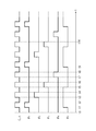
- the clock supply unit 25 generates and outputs a clock signal CLK that periodically repeats rising and falling.
- the rise or fall timing of the sub clock signal ⁇ i is as follows.
- the clock signal CLK falls until the nth fall, such as at the time of the fall.
- the example of FIG. 6 shows an example in which the sub-clock signal ⁇ 0 is controlled to fall at the rising timing of the clock signal CLK immediately before the time of n / 2 + 1 times from the time point t9, that is, the third falling time.
- the clock supply unit 25 supplies the subclock signal ⁇ 1 from the first three-state buffer 21_1 to the eighth three-state buffer 21_8, and the subclock signal ⁇ 2 from the ninth three-state buffer 21_9 to the sixteenth.
- the sub clock ⁇ i is supplied to each of the eight three-state buffers 21 _ ([i / 8] +1).
- [*] means the maximum integer not exceeding *.
- the operation of the three-state buffer 21 and the clock supply unit 25 receives an input of a bit string of M (M is an integer of M> N) bit length, extracts an N-bit bit string from the bit string, Dividing means for outputting the extracted N-bit bit string to the memory device 12 in a time division manner is realized.
- the output unit 31 of the output unit 30 is the timing at which the clock signal CLK input from the clock supply unit 25 falls, and the sub clock signal ⁇ n (n is the number of bits 8n to be subjected to a logical operation, and the memory device 12 At a timing at which the address bus width divided by 8) does not fall, a 1-bit signal output from the flip-flop circuit unit 32 is received and held in a buffer (not shown).
- the output unit 31 reads data stored at an address represented by the bit string output from the three-state buffer 21 among the data stored in the memory device 12 at the next timing when the clock signal CLK rises.
- the output unit 31 selectively selects either the logical operation result or its inverted bit from the read data depending on whether the 1-bit signal held in the buffer is “0” or “1”. Output.
- the output unit 31 outputs the MSB bit (logical operation result) of the data read from the memory device 12 to the switch unit 33 when the bit held in the buffer is “0”. To do. In addition, when the bit held in the buffer is “1”, the output unit 31 switches the next bit of the MSB (bit storing the inverted bit of the logical operation result) in the data read from the memory device 12. To the unit 33. The output unit 31 continues this output until the clock signal CLK falls next time.
- the output unit 31 controls a switch unit 33 which will be described later. Specifically, the output unit 31 rises a sub clock signal ⁇ n output from the clock supply unit 25 (n is a value obtained by dividing the number of bits 8n to be subjected to logical operation by 8 which is the address bus width of the memory device 12). At the timing, the output destination of the switch unit 33 described later is set to output to the outside. Then, the output destination of the switch unit 33 is set in the flip-flop circuit unit 32 at the timing when the clock signal CLK output from the clock supply unit 25 rises.
- the output unit 31 holds a bit of “0” in the buffer regardless of the output of the flip-flop circuit unit 32 at the timing when the sub clock signal ⁇ n output from the clock supply unit 25 falls. This operation is hereinafter referred to as an output unit reset operation.
- the flip-flop circuit unit 32 includes, for example, a D-type flip-flop circuit. Specifically, in the flip-flop circuit 24, the D terminal (input terminal) receives the output of the output unit 31. The C terminal (clock terminal) receives the clock signal CLK from the clock supply unit 25. The flip-flop circuit unit 32 holds a bit input to the D terminal, which is an input terminal, and outputs a signal of the bit to the output terminal Q at the timing when the clock signal CLK rises. This output is continued even when the clock signal CLK falls. A bit output from the output terminal Q is input to the output unit 31 as an output from the flip-flop circuit unit 32.
- the switch unit 33 accepts control from the output unit 31 and selectively outputs the 1-bit information input from the output unit 31 to either the flip-flop circuit unit 32 or the outside.
- the logical operation device 1 operates as follows. That is, when the reset operation of the output unit is performed (time t0 in FIG. 6), the output unit 31 holds the bit “0” in the buffer. Next, at the timing when the clock signal CLK output from the clock supply unit 25 rises (time t1 in FIG. 6), the three-state buffers 21_1 to 21_8 use the input bits b1, b2,. To supply.
- the output unit 31 reads the data stored in the address represented by the bit string output from the three-state buffers 21_1 to 21_8 among the data stored in the memory device 12. At this time, since the buffer of the output unit 31 holds the bit “0”, the output unit 31 calculates the MSB bit (logical operation result) of the data read from the memory device 12 in the first operation. Output as the result R1.
- the output R 1 is output to the flip-flop circuit unit 32 via the switch unit 33 and is held in the flip-flop circuit unit 32.
- the outputs of the three-state buffers 21_1 to 21_8 become high impedance.
- the output unit 31 receives the previous calculation result R1 from the flip-flop circuit unit 32 and holds it in the buffer.
- the three-state buffers 21_9 to 21_16 transfer the input bits b9, b10,... B16 to the address bus of the memory device 12. To supply.
- the output unit 31 reads the data stored in the address represented by the bit string output from the three-state buffers 21_9 to 21_16 among the data stored in the memory device 12.
- the output unit 31 When the buffer holds a bit of “0” (when the operation result R 1 is “0”), the output unit 31 outputs the MSB bit (logic) of the data read from the memory device 12. The calculation result is output as the second calculation result R2.
- the output unit 31 when the buffer holds the bit “1” (when the operation result R1 is “1”), the output unit 31 outputs the next bit of the MSB in the data read from the memory device 12. (The inverted bit of the logical operation result) is output as the second operation result R2.
- the output R 2 is output to the flip-flop circuit unit 32 via the switch unit 33 and is held in the flip-flop circuit unit 32.
- the output unit 31 sets the output destination of the switch unit 33 to output to the outside at the timing when the sub clock signal ⁇ n output from the clock supply unit 25 rises.
- the output unit 31 stores the data stored in the memory device 12 at the address indicated by the bit string output from the three-state buffers 21_ (8 ⁇ (n ⁇ 1) +1) to 21_ (8n). Read data.
- the buffer holds a bit of “0” (when the calculation result Rn ⁇ 1 is “0”), the output unit 31 stores the MSB bit in the data read from the memory device 12.
- the (logical operation result) is output as the operation result R.
- the output unit 31 outputs the next MSB of the data read from the memory device 12. (The inverted bit of the logical operation result) is output as the operation result R. This output is supplied to the outside via the switch unit 33.
- the output unit 31 performs the reset operation of the output unit at the next timing when the clock signal CLK falls, and further sets the output destination of the switch unit 33 in the flip-flop circuit unit 32 at the next timing when the clock signal CLK rises.
- the output unit 31 accesses the memory device using the previously output bit at the timing when the N-bit bit string is output in a time division manner. It functions as a means for selectively outputting one of the logical operation result between them and the inverted bit.
- the output unit 31 outputs the logical operation result (exclusive OR in this example) of each bit included in the data D having a length of 8 ⁇ n bits as the operation result R.
- the example of the output unit in the case of performing the operation in a time division manner is not limited to this example. That is, since the data that can be stored in each address of the memory device 12 is 8 bits, it is possible to make the following configuration by utilizing this bit width.
- the logical operation device 1 includes 8 ⁇ n three-state buffers 21 (here, the address bus width N of the memory device 12 is 8). (Similar to the example illustrated in FIG. 5, the three-state buffer unit 20 is configured with eight units each), the memory device 12, the clock supply unit 25, and the output unit 40.
- the output unit 40 includes four selector units 41a, b, c, and d (1/2 of the data bus width L of the memory device 12).
- components having the same configurations as those already described are denoted by the same reference numerals and description thereof is omitted.
- bit string a1, a2 from the MSB side at the position indicated by the 8-bit long address A (represented by the bit string a1, a2,... A8). ,... A set of a logical operation result based on a8 and its inverted bit are repeatedly arranged. That is, in this example, the logical operation result is stored in the odd-numbered bit of the data stored at the position of each address, and the inverted bit of the bit in the odd-numbered bit is stored in the even-numbered bit.
- the selector unit 41a of the output unit 40 is connected to signal lines of d1 which is the MSB and d2 which is the next bit of the MSB in the data bus of the memory device 12.
- the selector unit 41a accepts a 1-bit signal input from the outside.
- the selector unit 41a stores the data stored in the memory device 12 at the address represented by the bit string output from the three-state buffer 21 at the timing when the sub clock signal ⁇ 1 input from the clock supply unit 25 rises. Read and latch the data. The selector unit 41a selects one bit of the MSB representing the logical operation result or the inverse of the read data depending on whether the 1-bit signal received from the outside is “0” or “1”. Any one bit of the next MSB representing the bit is selectively latched and output.
- the selector unit 41 a selects the MSB bit (the logical operation result output by the signal line d 1) from the data read from the memory device 12. Latch and output.
- the selector unit 41a outputs the bit next to the MSB (output of the signal line d2 representing the inverted bit of the logical operation result) in the data read from the memory device 12. Select, latch, and output.
- the selector unit 41b is connected to each signal line of d3 on the MSB side of the data bus of the memory device 12 and d4 which is the next bit.
- the selector unit 41b accepts a 1-bit signal output from the selector unit 41a.
- the selector unit 41b stores the data stored in the memory device 12 at the address represented by the bit string output from the three-state buffer 21 at the timing when the sub clock signal ⁇ 2 input from the clock supply unit 25 rises. Read and latch the data. Depending on whether the 1-bit signal received from the selector unit 41a is “0” or “1”, the selector unit 41b has 1 bit on the MSB side representing the logical operation result among the read data, Alternatively, one of the next 1 bits representing the inverted bit is selectively latched and output.
- the selector unit 41b when the bit received from the selector unit 41a is “0”, the selector unit 41b is the MSB side bit (the logical operation result output from the signal line d3) of the data read from the memory device 12. Is selected, latched, and output.
- the selector unit 41b represents a bit (inverted logical operation result) of the data read from the memory device 12 and represented by the signal line d4 next to the signal line d3. (Represents bit) is selected, latched, and output.
- the selector unit 41c is connected to each signal line of d5 on the MSB side of the data bus of the memory device 12 and d6 which is the next bit.
- the selector unit 41c accepts a 1-bit signal output from the selector unit 41b.
- the selector unit 41c is stored at the address represented by the bit string output from the three-state buffer 21 among the data stored in the memory device 12 at the timing when the sub clock signal ⁇ 3 input from the clock supply unit 25 rises. Read and latch the data.
- the selector unit 41c selects the MSB side bit (the logical operation result output by the signal line d5) from the data read from the memory device 12. To latch and output.
- the selector unit 41c has a bit (inverted bit of the logical operation result) represented by the signal line d6 next to the signal d5 in the data read from the memory device 12. Is selected, latched, and output.
- each signal line of d7 on the MSB side and d8 which is the next bit in the data bus of the memory device 12 is connected to the selector unit 41d.
- the selector unit 41d accepts a 1-bit signal output from the selector unit 41c.
- the selector unit 41d is stored at the address represented by the bit string output from the three-state buffer 21 among the data stored in the memory device 12 at the timing when the sub clock signal ⁇ 4 input from the clock supply unit 25 rises. Read and latch the data.
- the selector unit 41d selects the MSB side bit (the logical operation result output by the signal line d7) from the data read from the memory device 12. To latch and output.
- the selector unit 41c has a bit (inverted bit of the logical operation result) represented by the signal line d8 next to the signal d7 in the data read from the memory device 12. Is selected, latched, and output.
- the output of the selector unit 41d is output to the outside.
- the logical operation device 1 operates as follows. After the output of the selector unit 41d (time t0 in FIG. 6), the three-state buffer 21_1 at the next timing (time t1 in FIG. 6) at which the clock signal CLK and the sub clock signal ⁇ 1 output from the clock supply unit 25 rise. 21_8 supply the input bits b1, b2,..., B8 to the address bus of the memory device 12.
- the selector unit 41a of the output unit 40 reads the data stored in the address represented by the bit string output from the three-state buffers 21_1 to 21_8 among the data stored in the memory device 12.
- the selector unit 41a includes a latch, and the MSB bit (data bus signal line d1) is output from the data read from the memory device 12 at a timing when the sub clock signal ⁇ 1 rises (time t1 in FIG. 6). Data, that is, a logical operation result) is latched and output as an operation result R1.
- the output R1 is output to the selector unit 41b.
- the selector unit 41b accepts this output R1.
- the three-state buffers 21_9 to 21_16 store the input bits b9, b10,. To the address bus of the memory device 12.
- the selector unit 41b reads out data stored in the address represented by the bit string output from the three-state buffers 21_9 to 21_16 among the data stored in the memory device 12. Then, when the bit input from the selector unit 41a is “0” (when the calculation result R1 is “0”), the selector unit 41b includes the MSB side bits of the data read from the memory device 12. (The output of the signal line d3 on the data bus, that is, the logical operation result) is latched and output at the timing (time t3 in FIG. 6) when the subclock signal ⁇ 2 rises as the operation result R2.
- the selector unit 41b receives the d4 signal out of the data read from the memory device 12 when the bit input from the selector unit 41a is “1” (when the calculation result R1 is “1”).
- the output of the line (inverted bit of the logical operation result) is latched and output at the timing (time t3 in FIG. 6) when the subclock signal ⁇ 2 rises as the operation result R2.
- This output R2 is accepted by the selector unit 41c.
- the selector unit 41c operates in the same manner.
- the selector unit 41d Of the data stored in the memory device 12, the data stored in the address represented by the bit string output from the three-state buffers 21_25 to 21_32 is read.
- the selector unit 41d includes the MSB side bits of the data read from the memory device 12. (Output on the d7 signal line on the data bus, ie, logical operation result) is latched and output as the operation result R at the timing when the subclock signal ⁇ 4 rises. Further, the selector unit 41d receives the d8 signal out of the data read from the memory device 12 when the bit input from the selector unit 41c is “1” (when the calculation result R3 is “1”). The line output (inverted bit of the logical operation result) is latched and output as the operation result R at the timing when the subclock signal ⁇ 4 rises.
- each selector unit 41 included in the output unit 40 uses the previously output bit at the timing when the bit string of N bits is output in a time-sharing manner. It functions as means for selectively outputting one of a logical operation result between bits taken out by accessing the device and its inverted bit.
- the bit that is obtained by accessing the memory device using the previously output bit is extracted. It functions as a means for selectively outputting one of the logical operation result between them and the inverted bit.
- the present embodiment is not limited to this.
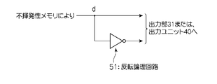
- a logical operation result using a signal line d output from the memory device 12 (a bit string represented by an address input to the memory device 12). May be connected to an inverted logic (NOT) circuit 51 to obtain an inverted bit of a logical operation result using a bit string represented by an address input to the memory device 12.
- NOT inverted logic
- the output unit 31 or the output unit 40 selects either the signal line d or the output of the inverting logic circuit 51 using the output of the previous stage (the output unit 40 latches it). Will be output.
- the address bus width is 8 bits
- n 4
- 8 logical operation devices 1 are arranged in parallel, and the output is further input to an 8-input logical operation circuit. Then, a logical operation of N ⁇ n ⁇ 8 bit length may be performed.
- FIG. 10 shows a look-up in the memory device 12
- the 1-bit output output by each logical operation device 1 is input to the same 8-input exclusive OR circuit 100 as illustrated in FIG. 11, and the exclusive OR operation is performed.
- the result is 1 bit.
Abstract
Le problème décrit par la présente invention est d'obtenir un dispositif arithmétique logique qui peut réaliser une opération de calcul en un temps relativement court à l'aide d'une configuration de circuit de taille relativement réduite. La solution selon l'invention porte sur un dispositif arithmétique logique qui : comprend un dispositif de mémoire (12) recevant une entrée d'une chaîne de bits qui a une longueur binaire égale à N (N étant un nombre entier supérieur ou égal à 2) et mémorisant, dans une adresse représentée par la chaîne de bits entrée, une table de conversion qui contient des données de plusieurs longueurs binaires incluant, dans une partie, des bits qui représentent le résultat d'une opération logique entre chacun des bits contenus dans la chaîne de bits entrée ; accède au dispositif de mémoire (12) ; et émet les bits contenus dans les données mémorisées à l'adresse représentée par la chaîne de bits reçue.
Priority Applications (3)
| Application Number | Priority Date | Filing Date | Title |
|---|---|---|---|
| EP14831256.4A EP3029839B1 (fr) | 2013-07-29 | 2014-06-09 | Dispositif arithmétique logique |
| CN201480042802.7A CN105432018B (zh) | 2013-07-29 | 2014-06-09 | 逻辑运算装置 |
| US14/908,339 US9866219B2 (en) | 2013-07-29 | 2014-06-09 | Device for logic operation |
Applications Claiming Priority (2)
| Application Number | Priority Date | Filing Date | Title |
|---|---|---|---|
| JP2013-157090 | 2013-07-29 | ||
| JP2013157090A JP6219631B2 (ja) | 2013-07-29 | 2013-07-29 | 論理演算装置 |
Publications (1)
| Publication Number | Publication Date |
|---|---|
| WO2015015905A1 true WO2015015905A1 (fr) | 2015-02-05 |
Family
ID=52431449
Family Applications (1)
| Application Number | Title | Priority Date | Filing Date |
|---|---|---|---|
| PCT/JP2014/065245 WO2015015905A1 (fr) | 2013-07-29 | 2014-06-09 | Dispositif arithmétique logique |
Country Status (6)
| Country | Link |
|---|---|
| US (1) | US9866219B2 (fr) |
| EP (1) | EP3029839B1 (fr) |
| JP (1) | JP6219631B2 (fr) |
| CN (1) | CN105432018B (fr) |
| TW (1) | TWI562059B (fr) |
| WO (1) | WO2015015905A1 (fr) |
Cited By (1)
| Publication number | Priority date | Publication date | Assignee | Title |
|---|---|---|---|---|
| CN113961170A (zh) * | 2020-07-21 | 2022-01-21 | 美光科技公司 | 存储器中的算术操作 |
Families Citing this family (2)
| Publication number | Priority date | Publication date | Assignee | Title |
|---|---|---|---|---|
| US10990389B2 (en) * | 2019-04-29 | 2021-04-27 | Micron Technology, Inc. | Bit string operations using a computing tile |
| US10778245B1 (en) * | 2019-08-20 | 2020-09-15 | Micron Technology, Inc. | Bit string conversion |
Citations (3)
| Publication number | Priority date | Publication date | Assignee | Title |
|---|---|---|---|---|
| JPH0457112A (ja) * | 1990-06-26 | 1992-02-24 | Mitsubishi Electric Corp | 演算装置 |
| JPH09292990A (ja) * | 1996-04-26 | 1997-11-11 | Nippon Telegr & Teleph Corp <Ntt> | 論理演算ユニット |
| JP2010165179A (ja) * | 2009-01-15 | 2010-07-29 | Hiroshima Univ | 半導体装置 |
Family Cites Families (18)
| Publication number | Priority date | Publication date | Assignee | Title |
|---|---|---|---|---|
| JP2853154B2 (ja) * | 1988-08-19 | 1999-02-03 | 富士ゼロックス株式会社 | プログラマブル・ファジィ論理回路 |
| US6049223A (en) * | 1995-03-22 | 2000-04-11 | Altera Corporation | Programmable logic array integrated circuit with general-purpose memory configurable as a random access or FIFO memory |
| US6487190B1 (en) * | 1996-06-27 | 2002-11-26 | Interdigital Technology Corporation | Efficient multichannel filtering for CDMA modems |
| GB9900432D0 (en) * | 1999-01-08 | 1999-02-24 | Xilinx Inc | Linear feedback shift register in a progammable gate array |
| US6555398B1 (en) * | 1999-10-22 | 2003-04-29 | Magic Corporation | Software programmable multiple function integrated circuit module |
| US6463003B2 (en) * | 2000-06-07 | 2002-10-08 | Advanced Micro Devices, Inc. | Power saving scheme for burst mode implementation during reading of data from a memory device |
| US7111224B1 (en) * | 2001-02-28 | 2006-09-19 | Xilinx, Inc. | FPGA configuration memory with built-in error correction mechanism |
| US20030068038A1 (en) * | 2001-09-28 | 2003-04-10 | Bedros Hanounik | Method and apparatus for encrypting data |
| JP2003281516A (ja) * | 2002-03-22 | 2003-10-03 | Canon Inc | 画像処理装置及びその方法 |
| US7157933B1 (en) * | 2004-02-14 | 2007-01-02 | Herman Schmit | Configurable circuits, IC's, and systems |
| US7330050B2 (en) * | 2004-11-08 | 2008-02-12 | Tabula, Inc. | Storage elements for a configurable IC and method and apparatus for accessing data stored in the storage elements |
| US7129864B2 (en) * | 2004-12-31 | 2006-10-31 | Intel Corporation | Fast compact decoder for huffman codes |
| WO2006075218A2 (fr) * | 2005-01-14 | 2006-07-20 | Nxp B.V. | Codage de canal |
| JP4827695B2 (ja) * | 2006-11-13 | 2011-11-30 | パナソニック株式会社 | 無線受信装置 |
| US7768430B1 (en) * | 2008-05-20 | 2010-08-03 | Altera Corporation | Look-up table based memory |
| US7663957B2 (en) * | 2008-05-27 | 2010-02-16 | Via Technologies, Inc. | Microprocessor with program-accessible re-writable non-volatile state embodied in blowable fuses of the microprocessor |
| US9747105B2 (en) * | 2009-12-17 | 2017-08-29 | Intel Corporation | Method and apparatus for performing a shift and exclusive or operation in a single instruction |
| WO2013062975A1 (fr) * | 2011-10-24 | 2013-05-02 | Skyworks Solutions, Inc. | Interface de commande bimode pour amplificateur de puissance |
-
2013
- 2013-07-29 JP JP2013157090A patent/JP6219631B2/ja active Active
-
2014
- 2014-06-03 TW TW103119252A patent/TWI562059B/zh active
- 2014-06-09 US US14/908,339 patent/US9866219B2/en active Active
- 2014-06-09 CN CN201480042802.7A patent/CN105432018B/zh active Active
- 2014-06-09 EP EP14831256.4A patent/EP3029839B1/fr active Active
- 2014-06-09 WO PCT/JP2014/065245 patent/WO2015015905A1/fr active Application Filing
Patent Citations (3)
| Publication number | Priority date | Publication date | Assignee | Title |
|---|---|---|---|---|
| JPH0457112A (ja) * | 1990-06-26 | 1992-02-24 | Mitsubishi Electric Corp | 演算装置 |
| JPH09292990A (ja) * | 1996-04-26 | 1997-11-11 | Nippon Telegr & Teleph Corp <Ntt> | 論理演算ユニット |
| JP2010165179A (ja) * | 2009-01-15 | 2010-07-29 | Hiroshima Univ | 半導体装置 |
Non-Patent Citations (1)
| Title |
|---|
| 74LVC1G386 3-INPUT EXCLUSIVE-OR GATE, 3 September 2007 (2007-09-03), Retrieved from the Internet <URL:http://www.jp.nxp.com/documents/data_sheet/74LVC1G386.pdf> |
Cited By (2)
| Publication number | Priority date | Publication date | Assignee | Title |
|---|---|---|---|---|
| CN113961170A (zh) * | 2020-07-21 | 2022-01-21 | 美光科技公司 | 存储器中的算术操作 |
| CN113961170B (zh) * | 2020-07-21 | 2022-11-11 | 美光科技公司 | 存储器中的算术操作 |
Also Published As
| Publication number | Publication date |
|---|---|
| JP6219631B2 (ja) | 2017-10-25 |
| US9866219B2 (en) | 2018-01-09 |
| EP3029839A1 (fr) | 2016-06-08 |
| US20160211851A1 (en) | 2016-07-21 |
| CN105432018B (zh) | 2019-01-08 |
| CN105432018A (zh) | 2016-03-23 |
| EP3029839B1 (fr) | 2018-05-30 |
| TW201506779A (zh) | 2015-02-16 |
| TWI562059B (en) | 2016-12-11 |
| JP2015026341A (ja) | 2015-02-05 |
| EP3029839A4 (fr) | 2017-04-19 |
Similar Documents
| Publication | Publication Date | Title |
|---|---|---|
| JP5141910B2 (ja) | Sms4暗号アルゴリズムを実現する暗号化および復号化処理方法とそのシステム | |
| CN107437945B (zh) | 并串转换电路 | |
| KR20010062206A (ko) | 논리회로 | |
| WO2015015905A1 (fr) | Dispositif arithmétique logique | |
| US9166795B2 (en) | Device and method for forming a signature | |
| JP3250550B2 (ja) | パスメモリ回路およびビタビ復号回路 | |
| JP4842989B2 (ja) | プライオリティエンコーダならびにそれを利用した時間デジタル変換器、試験装置 | |
| US7692564B2 (en) | Serial-to-parallel conversion circuit and method of designing the same | |
| US8433986B2 (en) | Method and apparatus for low latency turbo code encoding | |
| JP2015026341A5 (fr) | ||
| TWI240199B (en) | Interstitial product generator, multiplication circuit and multiplication method for bit segments | |
| JP6463169B2 (ja) | 電子回路およびカメラ | |
| RU154062U1 (ru) | Устройство для перебора перестановок | |
| US10170166B1 (en) | Data transmission apparatus for memory and data transmission method thereof | |
| JP5059968B2 (ja) | A/d変換装置 | |
| US8023614B2 (en) | Counting circuit and address counter using the same | |
| KR970049702A (ko) | 고속 배럴쉬프터 | |
| JPH11317676A (ja) | 有限フィ―ルドでの任意要素の逆数具現回路 | |
| KR101975576B1 (ko) | 복수의 제어 대상을 제어하는 제어 장치 | |
| JP2005073146A (ja) | Crcチェック回路 | |
| WO2022048245A1 (fr) | Circuit de génération de nombres aléatoires | |
| CN108540138B (zh) | 一种csraa编码电路及编码器 | |
| JPH0644051A (ja) | マイクロコンピュータ | |
| JP2019149070A (ja) | シリアルインタフェース回路、半導体装置、及びシリアルパラレル変換方法 | |
| JPH06290584A (ja) | 半導体記憶装置 |
Legal Events
| Date | Code | Title | Description |
|---|---|---|---|
| WWE | Wipo information: entry into national phase |
Ref document number: 201480042802.7 Country of ref document: CN |
|
| 121 | Ep: the epo has been informed by wipo that ep was designated in this application |
Ref document number: 14831256 Country of ref document: EP Kind code of ref document: A1 |
|
| WWE | Wipo information: entry into national phase |
Ref document number: 14908339 Country of ref document: US |
|
| NENP | Non-entry into the national phase |
Ref country code: DE |
|
| WWE | Wipo information: entry into national phase |
Ref document number: 2014831256 Country of ref document: EP |