WO2015015905A1 - Arithmetic logic device - Google Patents
Arithmetic logic device Download PDFInfo
- Publication number
- WO2015015905A1 WO2015015905A1 PCT/JP2014/065245 JP2014065245W WO2015015905A1 WO 2015015905 A1 WO2015015905 A1 WO 2015015905A1 JP 2014065245 W JP2014065245 W JP 2014065245W WO 2015015905 A1 WO2015015905 A1 WO 2015015905A1
- Authority
- WO
- WIPO (PCT)
- Prior art keywords
- bit
- output
- unit
- logical operation
- memory device
- Prior art date
Links
Images
Classifications
-
- H—ELECTRICITY
- H03—ELECTRONIC CIRCUITRY
- H03K—PULSE TECHNIQUE
- H03K19/00—Logic circuits, i.e. having at least two inputs acting on one output; Inverting circuits
- H03K19/20—Logic circuits, i.e. having at least two inputs acting on one output; Inverting circuits characterised by logic function, e.g. AND, OR, NOR, NOT circuits
- H03K19/21—EXCLUSIVE-OR circuits, i.e. giving output if input signal exists at only one input; COINCIDENCE circuits, i.e. giving output only if all input signals are identical
-
- G—PHYSICS
- G06—COMPUTING; CALCULATING OR COUNTING
- G06F—ELECTRIC DIGITAL DATA PROCESSING
- G06F1/00—Details not covered by groups G06F3/00 - G06F13/00 and G06F21/00
- G06F1/02—Digital function generators
Definitions
- the present invention relates to a logical operation device that performs a logical operation between bits included in an input bit string.
- an exclusive OR operation device for multi-bit length data is configured by combining two-input exclusive OR circuits.
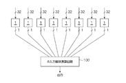
- FIG. 11 shows an example of a logical operation device that calculates an exclusive OR of 32 bits.
- the logical operation device that calculates the 32-bit exclusive OR includes four 8-input exclusive OR circuits 100 and three 2-input exclusive OR circuits 200. .
- the 8-input exclusive OR circuit 100 includes seven 2-input exclusive OR circuits 200 therein.
- Non-Patent Document 1 An example of a multi-input (3-input) exclusive OR gate is disclosed in Non-Patent Document 1.
- the present invention has been made in view of the above circumstances, and provides a logical operation device capable of performing arithmetic processing in a relatively short time with a relatively small circuit configuration even for multi-bit data. This is one of its purposes.
- the present invention for solving the problems of the above conventional example is a logical operation device, which accepts an input of a bit string having a bit length of N (N is an integer of N ⁇ 2) and represents the input bit string
- a memory device for storing a lookup table formed by storing, in an address, multi-bit data including a bit representing a logical operation result between bits included in the input bit string, and the memory device; And an output means for outputting a bit included in data stored at an address represented by the received bit string.
- arithmetic processing can be performed in a relatively short time with a relatively small circuit configuration.
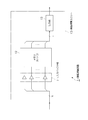
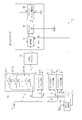
- the logical operation device 1 includes at least one logical operation unit 10 as illustrated in FIG.
- the logical operation unit 10 basically includes an input buffer unit 11, a memory device 12, and an output unit 13.
- the input buffer unit 11 accepts an input of a bit string having a bit length of N (N is an integer of N ⁇ 2) and supplies a signal represented by the bit string to the address bus of the memory device 12. That is, in this example, N corresponds to the address bus width of the memory device 12.
- the memory device 12 is a semiconductor memory such as a nonvolatile memory or an SRAM (Static Random Access Memory), and includes memory cells of 2 N bits ⁇ L bits (L is an integer of L ⁇ 2).
- Data “0XXXXXX” (here, X may be indefinite) including “0”, which is the sum operation result, is stored.
- the address represented by the bit string “00000001” includes data “1XXXXXXXX” (X is indefinite) that includes “1”, which is the operation result of the exclusive OR of the bit string “00000001”, in the MSB (most significant bit). Good) is stored.
- the output unit 13 reads the data stored in the address represented by the bit string output from the input buffer unit 11 among the data stored in the memory device 12.
- the output unit 13 selectively outputs a bit including the logical operation result in the read data.
- the output unit 13 since the logical operation result is included in the MSB, the output unit 13 stores the data stored in the memory device at the address represented by the bit string output by the input buffer unit 11. The read data is read, and the MSB bit of the data is output.
- the memory device 12 includes a bit representing a logical operation result between each bit included in the input bit string at an address represented by the bit string input from the input buffer unit 11.
- a look-up table is stored which stores multi-bit length data including the inverted bit as a part thereof.
- Data “01XXXXXX” (here, X may be indefinite) including “0” that is the sum operation result and “1” that is the inverted bit of this operation result is stored in the next bit.
- the address represented by the bit string “00000001” includes “1” that is the result of the exclusive OR of the bit string “00000001” in its MSB (most significant bit), and the next bit is the inverted bit.
- Data “10XXXXXXX” (“X” may be indefinite) including “0” is stored.
- the output unit 13 accepts a 1-bit signal input from the outside.
- the output unit 13 reads the data stored in the address represented by the bit string output from the input buffer unit 11 among the data stored in the memory device 12, and the 1-bit signal input from the outside is “0”. "1” or "1”, the logical operation result or its inverted bit is selectively output from the data.
- the output unit 13 is a bit string output from the input buffer unit 11 among the data stored in the memory device when the 1-bit signal input from the outside is “0”. The data stored at the address indicated by is read, and the MSB bit of the data is output.
- the output unit 13 is stored in the address represented by the bit string output from the input buffer unit 11 among the data stored in the memory device.
- the data is read, and the next bit of the MSB of the data (the bit storing the inverted bit of the logical operation result) is output.
- This embodiment basically has the above configuration and operates as in the following example.
- a plurality of logical operation units 10_1, 10_2,... 10_n are provided as illustrated in FIG.
- the output unit 13_i of the i-th logic operation unit 10_i accepts the output bit of the i-1th logic operation unit 10_i-1 as an input from the outside.
- the output unit 13_1 of the first logical operation unit 10_1 does not receive an external input (or fixes the external input to “0”, for example), and stores the data stored in the memory device 12. Of these, a bit representing the logical operation result (MSB in the above example) is output.
- the output unit 13_1 of the logical operation unit 10_1 is stored in the address represented by the 8-bit long bit string (b1, b2,..., B8) input to the input buffer 11_1 among the data stored in the memory device 12_1. Read data. Then, the bits of the logical operation result (here, the operation result of the exclusive OR of the input 8-bit length bit string) included in the read data are output.
- the output unit 13_2 of the next logical operation unit 10_2 is stored at the address represented by the 8-bit long bit string (b9, b10,..., B16) input to the input buffer 11_2 among the data stored in the memory device 12_2.
- Read out data The output unit 13_2 selects and outputs either the bit of the logical operation result included in the read data or its inverted bit based on the bit output from the output unit 13_1 of the preceding logical operation unit 10_1. To do. Specifically, the output unit 13_2 outputs a logical operation result included in the read data when the bit output from the output unit 13_1 is “0”.
- the output unit 13_2 outputs an inverted bit of the logical operation result when the bit output from the output unit 13_1 is “1”.
- the output unit 13_i of the i-th logical operation unit 10_i uses the 8-bit length bit string (b8 (i-1) +1, b8) input to the input buffer 11_i among the data stored in the memory device 12_i. Read the data stored at the address indicated by (i-1) +2,..., b8i). Further, the output unit 13_i outputs either the bit of the logical operation result included in the read data or its inverted bit based on the bit output from the output unit 13_i-1 of the preceding logical operation unit 10_i-1. Select and output. Specifically, the output unit 13_i outputs a logical operation result included in the read data when the bit output from the output unit 13_i-1 is “0”. The output unit 13_i outputs an inverted bit of the logical operation result when the bit output from the output unit 13_i-1 is “1”.
- the output unit 13_n of the n-th logical operation unit 10_n includes an 8-bit length bit string (b8 (n-1) +1, b8 () input to the input buffer 11_n among the data stored in the memory device 12_n. n-1) +2,... b8n) reads data stored at the address indicated.
- the output unit 13_n outputs either the bit of the logical operation result included in the read data or its inverted bit based on the bit output from the output unit 13_n-1 of the preceding logical operation unit 10_n-1. Select and output. Specifically, the output unit 13_n outputs a logical operation result included in the read data when the bit output from the output unit 13_n ⁇ 1 is “0”.
- the output unit 13_n outputs an inverted bit of the logical operation result when the bit output from the output unit 13_n-1 is “1”.
- the output unit 13_n of the nth logical operation unit 10_n outputs a logical operation result (exclusive OR in this example) of each bit included in the data D having a length of 8 ⁇ n bits.
- the present embodiment is not limited to this.
- the memory device 12 may be used in a time division manner.
- the logical operation device 1 according to the embodiment of the present invention relating to this example includes n three-state buffer units 20, a memory device 12, a clock supply unit 25, and an output unit 30. It is comprised including.
- Including components having the same configurations as those already described are denoted by the same reference numerals and description thereof is omitted.
- the memory device 12 stores the data illustrated in FIG.
- the three-state buffer 21 includes an input terminal X, an output terminal Y, and a gate terminal G, respectively.
- the three-state buffer 21 sets the state of the output terminal Y to the high impedance state “Z” regardless of what is input to the input terminal X while the input of the gate terminal G is “0”.
- the three-state buffer 21 in which the output terminal Y has a high impedance is the same as an insulated state (a state in which the connection is disconnected).
- 8n three-state buffers 21 are a group from the first three-state buffer 21_1 to the eighth three-state buffer 21_8, and from the ninth three-state buffer 21_9 to the sixteenth.
- the groups up to the three-state buffer 21_16 are divided into eight groups.
- the same signal is input from the clock supply unit 25 to the gate terminals G of the three-state buffers 21 belonging to the same group. This signal will be described later.
- the value of each bit is input to the input terminal X_i of the i-th three-state buffer 21_i in order from the MSB side (or LSB side) of the data D of 8 ⁇ n bit length to be subjected to logical operation.
- the output terminal Y_i of the i-th three-state buffer 21_i is connected to the (i (mod 8) -th pin of the address bus of the memory device 12.
- (i mod k) means the remainder when i is divided by k.
- the clock supply unit 25 generates and outputs a clock signal CLK that periodically repeats rising and falling.
- the rise or fall timing of the sub clock signal ⁇ i is as follows.
- the clock signal CLK falls until the nth fall, such as at the time of the fall.
- the example of FIG. 6 shows an example in which the sub-clock signal ⁇ 0 is controlled to fall at the rising timing of the clock signal CLK immediately before the time of n / 2 + 1 times from the time point t9, that is, the third falling time.
- the clock supply unit 25 supplies the subclock signal ⁇ 1 from the first three-state buffer 21_1 to the eighth three-state buffer 21_8, and the subclock signal ⁇ 2 from the ninth three-state buffer 21_9 to the sixteenth.
- the sub clock ⁇ i is supplied to each of the eight three-state buffers 21 _ ([i / 8] +1).
- [*] means the maximum integer not exceeding *.
- the operation of the three-state buffer 21 and the clock supply unit 25 receives an input of a bit string of M (M is an integer of M> N) bit length, extracts an N-bit bit string from the bit string, Dividing means for outputting the extracted N-bit bit string to the memory device 12 in a time division manner is realized.
- the output unit 31 of the output unit 30 is the timing at which the clock signal CLK input from the clock supply unit 25 falls, and the sub clock signal ⁇ n (n is the number of bits 8n to be subjected to a logical operation, and the memory device 12 At a timing at which the address bus width divided by 8) does not fall, a 1-bit signal output from the flip-flop circuit unit 32 is received and held in a buffer (not shown).
- the output unit 31 reads data stored at an address represented by the bit string output from the three-state buffer 21 among the data stored in the memory device 12 at the next timing when the clock signal CLK rises.
- the output unit 31 selectively selects either the logical operation result or its inverted bit from the read data depending on whether the 1-bit signal held in the buffer is “0” or “1”. Output.
- the output unit 31 outputs the MSB bit (logical operation result) of the data read from the memory device 12 to the switch unit 33 when the bit held in the buffer is “0”. To do. In addition, when the bit held in the buffer is “1”, the output unit 31 switches the next bit of the MSB (bit storing the inverted bit of the logical operation result) in the data read from the memory device 12. To the unit 33. The output unit 31 continues this output until the clock signal CLK falls next time.
- the output unit 31 controls a switch unit 33 which will be described later. Specifically, the output unit 31 rises a sub clock signal ⁇ n output from the clock supply unit 25 (n is a value obtained by dividing the number of bits 8n to be subjected to logical operation by 8 which is the address bus width of the memory device 12). At the timing, the output destination of the switch unit 33 described later is set to output to the outside. Then, the output destination of the switch unit 33 is set in the flip-flop circuit unit 32 at the timing when the clock signal CLK output from the clock supply unit 25 rises.
- the output unit 31 holds a bit of “0” in the buffer regardless of the output of the flip-flop circuit unit 32 at the timing when the sub clock signal ⁇ n output from the clock supply unit 25 falls. This operation is hereinafter referred to as an output unit reset operation.
- the flip-flop circuit unit 32 includes, for example, a D-type flip-flop circuit. Specifically, in the flip-flop circuit 24, the D terminal (input terminal) receives the output of the output unit 31. The C terminal (clock terminal) receives the clock signal CLK from the clock supply unit 25. The flip-flop circuit unit 32 holds a bit input to the D terminal, which is an input terminal, and outputs a signal of the bit to the output terminal Q at the timing when the clock signal CLK rises. This output is continued even when the clock signal CLK falls. A bit output from the output terminal Q is input to the output unit 31 as an output from the flip-flop circuit unit 32.
- the switch unit 33 accepts control from the output unit 31 and selectively outputs the 1-bit information input from the output unit 31 to either the flip-flop circuit unit 32 or the outside.
- the logical operation device 1 operates as follows. That is, when the reset operation of the output unit is performed (time t0 in FIG. 6), the output unit 31 holds the bit “0” in the buffer. Next, at the timing when the clock signal CLK output from the clock supply unit 25 rises (time t1 in FIG. 6), the three-state buffers 21_1 to 21_8 use the input bits b1, b2,. To supply.
- the output unit 31 reads the data stored in the address represented by the bit string output from the three-state buffers 21_1 to 21_8 among the data stored in the memory device 12. At this time, since the buffer of the output unit 31 holds the bit “0”, the output unit 31 calculates the MSB bit (logical operation result) of the data read from the memory device 12 in the first operation. Output as the result R1.
- the output R 1 is output to the flip-flop circuit unit 32 via the switch unit 33 and is held in the flip-flop circuit unit 32.
- the outputs of the three-state buffers 21_1 to 21_8 become high impedance.
- the output unit 31 receives the previous calculation result R1 from the flip-flop circuit unit 32 and holds it in the buffer.
- the three-state buffers 21_9 to 21_16 transfer the input bits b9, b10,... B16 to the address bus of the memory device 12. To supply.
- the output unit 31 reads the data stored in the address represented by the bit string output from the three-state buffers 21_9 to 21_16 among the data stored in the memory device 12.
- the output unit 31 When the buffer holds a bit of “0” (when the operation result R 1 is “0”), the output unit 31 outputs the MSB bit (logic) of the data read from the memory device 12. The calculation result is output as the second calculation result R2.
- the output unit 31 when the buffer holds the bit “1” (when the operation result R1 is “1”), the output unit 31 outputs the next bit of the MSB in the data read from the memory device 12. (The inverted bit of the logical operation result) is output as the second operation result R2.
- the output R 2 is output to the flip-flop circuit unit 32 via the switch unit 33 and is held in the flip-flop circuit unit 32.
- the output unit 31 sets the output destination of the switch unit 33 to output to the outside at the timing when the sub clock signal ⁇ n output from the clock supply unit 25 rises.
- the output unit 31 stores the data stored in the memory device 12 at the address indicated by the bit string output from the three-state buffers 21_ (8 ⁇ (n ⁇ 1) +1) to 21_ (8n). Read data.
- the buffer holds a bit of “0” (when the calculation result Rn ⁇ 1 is “0”), the output unit 31 stores the MSB bit in the data read from the memory device 12.
- the (logical operation result) is output as the operation result R.
- the output unit 31 outputs the next MSB of the data read from the memory device 12. (The inverted bit of the logical operation result) is output as the operation result R. This output is supplied to the outside via the switch unit 33.
- the output unit 31 performs the reset operation of the output unit at the next timing when the clock signal CLK falls, and further sets the output destination of the switch unit 33 in the flip-flop circuit unit 32 at the next timing when the clock signal CLK rises.
- the output unit 31 accesses the memory device using the previously output bit at the timing when the N-bit bit string is output in a time division manner. It functions as a means for selectively outputting one of the logical operation result between them and the inverted bit.
- the output unit 31 outputs the logical operation result (exclusive OR in this example) of each bit included in the data D having a length of 8 ⁇ n bits as the operation result R.
- the example of the output unit in the case of performing the operation in a time division manner is not limited to this example. That is, since the data that can be stored in each address of the memory device 12 is 8 bits, it is possible to make the following configuration by utilizing this bit width.
- the logical operation device 1 includes 8 ⁇ n three-state buffers 21 (here, the address bus width N of the memory device 12 is 8). (Similar to the example illustrated in FIG. 5, the three-state buffer unit 20 is configured with eight units each), the memory device 12, the clock supply unit 25, and the output unit 40.
- the output unit 40 includes four selector units 41a, b, c, and d (1/2 of the data bus width L of the memory device 12).
- components having the same configurations as those already described are denoted by the same reference numerals and description thereof is omitted.
- bit string a1, a2 from the MSB side at the position indicated by the 8-bit long address A (represented by the bit string a1, a2,... A8). ,... A set of a logical operation result based on a8 and its inverted bit are repeatedly arranged. That is, in this example, the logical operation result is stored in the odd-numbered bit of the data stored at the position of each address, and the inverted bit of the bit in the odd-numbered bit is stored in the even-numbered bit.
- the selector unit 41a of the output unit 40 is connected to signal lines of d1 which is the MSB and d2 which is the next bit of the MSB in the data bus of the memory device 12.
- the selector unit 41a accepts a 1-bit signal input from the outside.
- the selector unit 41a stores the data stored in the memory device 12 at the address represented by the bit string output from the three-state buffer 21 at the timing when the sub clock signal ⁇ 1 input from the clock supply unit 25 rises. Read and latch the data. The selector unit 41a selects one bit of the MSB representing the logical operation result or the inverse of the read data depending on whether the 1-bit signal received from the outside is “0” or “1”. Any one bit of the next MSB representing the bit is selectively latched and output.
- the selector unit 41 a selects the MSB bit (the logical operation result output by the signal line d 1) from the data read from the memory device 12. Latch and output.
- the selector unit 41a outputs the bit next to the MSB (output of the signal line d2 representing the inverted bit of the logical operation result) in the data read from the memory device 12. Select, latch, and output.
- the selector unit 41b is connected to each signal line of d3 on the MSB side of the data bus of the memory device 12 and d4 which is the next bit.
- the selector unit 41b accepts a 1-bit signal output from the selector unit 41a.
- the selector unit 41b stores the data stored in the memory device 12 at the address represented by the bit string output from the three-state buffer 21 at the timing when the sub clock signal ⁇ 2 input from the clock supply unit 25 rises. Read and latch the data. Depending on whether the 1-bit signal received from the selector unit 41a is “0” or “1”, the selector unit 41b has 1 bit on the MSB side representing the logical operation result among the read data, Alternatively, one of the next 1 bits representing the inverted bit is selectively latched and output.
- the selector unit 41b when the bit received from the selector unit 41a is “0”, the selector unit 41b is the MSB side bit (the logical operation result output from the signal line d3) of the data read from the memory device 12. Is selected, latched, and output.
- the selector unit 41b represents a bit (inverted logical operation result) of the data read from the memory device 12 and represented by the signal line d4 next to the signal line d3. (Represents bit) is selected, latched, and output.
- the selector unit 41c is connected to each signal line of d5 on the MSB side of the data bus of the memory device 12 and d6 which is the next bit.
- the selector unit 41c accepts a 1-bit signal output from the selector unit 41b.
- the selector unit 41c is stored at the address represented by the bit string output from the three-state buffer 21 among the data stored in the memory device 12 at the timing when the sub clock signal ⁇ 3 input from the clock supply unit 25 rises. Read and latch the data.
- the selector unit 41c selects the MSB side bit (the logical operation result output by the signal line d5) from the data read from the memory device 12. To latch and output.
- the selector unit 41c has a bit (inverted bit of the logical operation result) represented by the signal line d6 next to the signal d5 in the data read from the memory device 12. Is selected, latched, and output.
- each signal line of d7 on the MSB side and d8 which is the next bit in the data bus of the memory device 12 is connected to the selector unit 41d.
- the selector unit 41d accepts a 1-bit signal output from the selector unit 41c.
- the selector unit 41d is stored at the address represented by the bit string output from the three-state buffer 21 among the data stored in the memory device 12 at the timing when the sub clock signal ⁇ 4 input from the clock supply unit 25 rises. Read and latch the data.
- the selector unit 41d selects the MSB side bit (the logical operation result output by the signal line d7) from the data read from the memory device 12. To latch and output.
- the selector unit 41c has a bit (inverted bit of the logical operation result) represented by the signal line d8 next to the signal d7 in the data read from the memory device 12. Is selected, latched, and output.
- the output of the selector unit 41d is output to the outside.
- the logical operation device 1 operates as follows. After the output of the selector unit 41d (time t0 in FIG. 6), the three-state buffer 21_1 at the next timing (time t1 in FIG. 6) at which the clock signal CLK and the sub clock signal ⁇ 1 output from the clock supply unit 25 rise. 21_8 supply the input bits b1, b2,..., B8 to the address bus of the memory device 12.
- the selector unit 41a of the output unit 40 reads the data stored in the address represented by the bit string output from the three-state buffers 21_1 to 21_8 among the data stored in the memory device 12.
- the selector unit 41a includes a latch, and the MSB bit (data bus signal line d1) is output from the data read from the memory device 12 at a timing when the sub clock signal ⁇ 1 rises (time t1 in FIG. 6). Data, that is, a logical operation result) is latched and output as an operation result R1.
- the output R1 is output to the selector unit 41b.
- the selector unit 41b accepts this output R1.
- the three-state buffers 21_9 to 21_16 store the input bits b9, b10,. To the address bus of the memory device 12.
- the selector unit 41b reads out data stored in the address represented by the bit string output from the three-state buffers 21_9 to 21_16 among the data stored in the memory device 12. Then, when the bit input from the selector unit 41a is “0” (when the calculation result R1 is “0”), the selector unit 41b includes the MSB side bits of the data read from the memory device 12. (The output of the signal line d3 on the data bus, that is, the logical operation result) is latched and output at the timing (time t3 in FIG. 6) when the subclock signal ⁇ 2 rises as the operation result R2.
- the selector unit 41b receives the d4 signal out of the data read from the memory device 12 when the bit input from the selector unit 41a is “1” (when the calculation result R1 is “1”).
- the output of the line (inverted bit of the logical operation result) is latched and output at the timing (time t3 in FIG. 6) when the subclock signal ⁇ 2 rises as the operation result R2.
- This output R2 is accepted by the selector unit 41c.
- the selector unit 41c operates in the same manner.
- the selector unit 41d Of the data stored in the memory device 12, the data stored in the address represented by the bit string output from the three-state buffers 21_25 to 21_32 is read.
- the selector unit 41d includes the MSB side bits of the data read from the memory device 12. (Output on the d7 signal line on the data bus, ie, logical operation result) is latched and output as the operation result R at the timing when the subclock signal ⁇ 4 rises. Further, the selector unit 41d receives the d8 signal out of the data read from the memory device 12 when the bit input from the selector unit 41c is “1” (when the calculation result R3 is “1”). The line output (inverted bit of the logical operation result) is latched and output as the operation result R at the timing when the subclock signal ⁇ 4 rises.
- each selector unit 41 included in the output unit 40 uses the previously output bit at the timing when the bit string of N bits is output in a time-sharing manner. It functions as means for selectively outputting one of a logical operation result between bits taken out by accessing the device and its inverted bit.
- the bit that is obtained by accessing the memory device using the previously output bit is extracted. It functions as a means for selectively outputting one of the logical operation result between them and the inverted bit.
- the present embodiment is not limited to this.
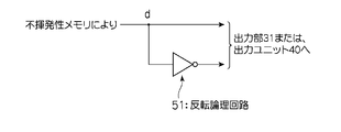
- a logical operation result using a signal line d output from the memory device 12 (a bit string represented by an address input to the memory device 12). May be connected to an inverted logic (NOT) circuit 51 to obtain an inverted bit of a logical operation result using a bit string represented by an address input to the memory device 12.
- NOT inverted logic
- the output unit 31 or the output unit 40 selects either the signal line d or the output of the inverting logic circuit 51 using the output of the previous stage (the output unit 40 latches it). Will be output.
- the address bus width is 8 bits
- n 4
- 8 logical operation devices 1 are arranged in parallel, and the output is further input to an 8-input logical operation circuit. Then, a logical operation of N ⁇ n ⁇ 8 bit length may be performed.
- FIG. 10 shows a look-up in the memory device 12
- the 1-bit output output by each logical operation device 1 is input to the same 8-input exclusive OR circuit 100 as illustrated in FIG. 11, and the exclusive OR operation is performed.
- the result is 1 bit.
Abstract
[Problem] To provide an arithmetic logic device capable of performing a computation operation in a relatively short time using a relatively small-scale circuit configuration. [Solution] An arithmetic logic device that: includes a memory device (12), which receives an input of a bit string having a bit length of N (where N is an integer equal to or greater than 2) and stores, in an address represented by the inputted bit string, a lookup table containing multi-bit-length data which includes, in a part thereof, bits representing the result of a logical operation between each of the bits contained in the inputted bit string; accesses the memory device (12); and outputs bits contained in the data stored at the address represented by the received bit string.
Description
本発明は、入力されるビット列に含まれるビット間の論理演算を行う論理演算装置に関する。
The present invention relates to a logical operation device that performs a logical operation between bits included in an input bit string.
情報処理技術、情報通信技術の発展・普及に伴い、より高速で、より大容量の情報処理技術が要求されている。例えば近年では、情報処理時の誤り訂正処理において、より多数ビット長のデータの誤り訂正を可能にすることが求められている。
With the development and popularization of information processing technology and information communication technology, higher speed and larger capacity information processing technology is required. For example, in recent years, it has been required to enable error correction of data having a larger number of bits in error correction processing during information processing.
この誤り訂正の際には、入力ビットのパリティチェック等のため、入力されたビット間の排他的論理和(XORまたはEOR)を求めることが必要となる。従来、多ビット長のデータに関する排他的論理和の演算装置は、2入力の排他的論理和回路を組み合わせて構成されていた。例えば、図11は、32ビット長の排他的論理和を演算する論理演算装置の例を示したものである。
In this error correction, it is necessary to obtain an exclusive OR (XOR or EOR) between input bits for parity check of input bits. Conventionally, an exclusive OR operation device for multi-bit length data is configured by combining two-input exclusive OR circuits. For example, FIG. 11 shows an example of a logical operation device that calculates an exclusive OR of 32 bits.
図11に例示するように、この32ビット長の排他的論理和を演算する論理演算装置は、4つの8入力排他的論理和回路100と、3つの2入力排他的論理和回路200とを含む。また8入力排他的論理和回路100は内部に、7つの2入力排他的論理和回路200を含んでなる。
As illustrated in FIG. 11, the logical operation device that calculates the 32-bit exclusive OR includes four 8-input exclusive OR circuits 100 and three 2-input exclusive OR circuits 200. . The 8-input exclusive OR circuit 100 includes seven 2-input exclusive OR circuits 200 therein.
なお、多入力(3入力)の排他的論理和ゲートの例が、非特許文献1に開示されている。
An example of a multi-input (3-input) exclusive OR gate is disclosed in Non-Patent Document 1.
しかしながら、近年ではますます多ビット長のデータ処理が要求されており、2入力排他的論理和回路の組み合わせによっては回路規模が大きくなり、また多段ゲートに構成することで演算処理時間も長くなってしまうという問題点があった。
However, in recent years, more and more multi-bit data processing is required, and the circuit scale increases depending on the combination of two-input exclusive OR circuits, and the arithmetic processing time also becomes longer due to the multi-stage gate configuration. There was a problem of end.
本発明は上記実情に鑑みて為されたもので、多ビット長のデータであっても比較的小規模な回路構成で、比較的短時間に演算処理を行うことができる論理演算装置を提供することを、その目的の一つとする。
The present invention has been made in view of the above circumstances, and provides a logical operation device capable of performing arithmetic processing in a relatively short time with a relatively small circuit configuration even for multi-bit data. This is one of its purposes.
上記従来例の問題点を解決するための本発明は、論理演算装置であって、N(Nは、N≧2の整数)ビット長のビット列の入力を受け入れて、前記入力されるビット列が表すアドレスに、当該入力されるビット列に含まれる各ビット間の論理演算結果を表すビットをその一部に含む多ビット長のデータを格納してなるルックアップテーブルを記憶するメモリデバイスと、前記メモリデバイスにアクセスし、前記受け入れたビット列が表すアドレスに格納されたデータに含まれるビットを出力する出力手段と、を含むこととしたものである。
The present invention for solving the problems of the above conventional example is a logical operation device, which accepts an input of a bit string having a bit length of N (N is an integer of N ≧ 2) and represents the input bit string A memory device for storing a lookup table formed by storing, in an address, multi-bit data including a bit representing a logical operation result between bits included in the input bit string, and the memory device; And an output means for outputting a bit included in data stored at an address represented by the received bit string.
本発明によると、比較的小規模な回路構成で、また比較的短時間に演算処理を行うことができる。
According to the present invention, arithmetic processing can be performed in a relatively short time with a relatively small circuit configuration.
本発明の実施の形態について図面を参照しながら説明する。本発明の実施の形態に係る論理演算装置1は、図1に例示するように少なくとも一つの論理演算ユニット10を含む。またこの論理演算ユニット10は、入力バッファ部11と、メモリデバイス12と、出力部13とを含んで基本的に構成される。
Embodiments of the present invention will be described with reference to the drawings. The logical operation device 1 according to the embodiment of the present invention includes at least one logical operation unit 10 as illustrated in FIG. The logical operation unit 10 basically includes an input buffer unit 11, a memory device 12, and an output unit 13.
入力バッファ部11は、N(Nは、N≧2の整数)ビット長のビット列の入力を受け入れて、このビット列の表す信号を、メモリデバイス12のアドレスバスに供給する。すなわち、ここでの例では、Nはメモリデバイス12のアドレスバス幅にも相当する。
The input buffer unit 11 accepts an input of a bit string having a bit length of N (N is an integer of N ≧ 2) and supplies a signal represented by the bit string to the address bus of the memory device 12. That is, in this example, N corresponds to the address bus width of the memory device 12.
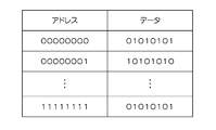
メモリデバイス12は、具体的には不揮発性メモリやSRAM(Static Random Access Memory)等の半導体メモリであり、2Nビット×Lビット(Lは、L≧2の整数)のメモリセルを備える。このメモリデバイス12は、その入力バッファ部11から入力されるビット列が表すアドレスに、当該入力されるビット列に含まれる各ビット間の論理演算結果を表すビットをその一部に含む多ビット長のデータを格納してなるルックアップテーブルを格納している。以下の例では、1つのアドレスによって特定される位置に、L=8ビットのデータが格納されるものとして説明する。
Specifically, the memory device 12 is a semiconductor memory such as a nonvolatile memory or an SRAM (Static Random Access Memory), and includes memory cells of 2 N bits × L bits (L is an integer of L ≧ 2). This memory device 12 is a multi-bit length data in which a bit representing a logical operation result between bits included in the input bit string is included in an address represented by the bit string input from the input buffer unit 11 as a part thereof. A lookup table is stored. In the following example, it is assumed that L = 8-bit data is stored at a position specified by one address.
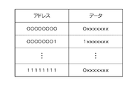
具体的に、このルックアップテーブルは図2に例示するように、N=8ビット長のビット列「00000000」が表すアドレスには、そのMSB(最上位ビット)に当該ビット列「00000000」の排他的論理和の演算結果である「0」を含んだデータ「0XXXXXXX」(ここでXは不定でよい)が格納される。また、ビット列「00000001」が表すアドレスには、そのMSB(最上位ビット)に当該ビット列「00000001」の排他的論理和の演算結果である「1」を含んだデータ「1XXXXXXX」(Xは不定でよい)が格納される。
Specifically, as illustrated in FIG. 2, in the lookup table, an address represented by a bit string “00000000” having an N = 8-bit length includes an exclusive logic of the bit string “00000000” in its MSB (most significant bit). Data “0XXXXXXX” (here, X may be indefinite) including “0”, which is the sum operation result, is stored. The address represented by the bit string “00000001” includes data “1XXXXXXXXX” (X is indefinite) that includes “1”, which is the operation result of the exclusive OR of the bit string “00000001”, in the MSB (most significant bit). Good) is stored.
出力部13は、メモリデバイス12が格納しているデータのうち、入力バッファ部11が出力するビット列が表すアドレスに格納されているデータを読み出す。この出力部13は当該読み出したデータのうち、上記論理演算結果が含まれるビットを選択的に出力する。本実施の形態の上述の例では、MSBに論理演算結果が含まれるので、この出力部13は、メモリデバイスが格納しているデータのうち、入力バッファ部11が出力するビット列が表すアドレスに格納されているデータを読み出し、当該データのうちのMSBのビットを出力する。
The output unit 13 reads the data stored in the address represented by the bit string output from the input buffer unit 11 among the data stored in the memory device 12. The output unit 13 selectively outputs a bit including the logical operation result in the read data. In the above example of the present embodiment, since the logical operation result is included in the MSB, the output unit 13 stores the data stored in the memory device at the address represented by the bit string output by the input buffer unit 11. The read data is read, and the MSB bit of the data is output.
また本実施の形態の別の例では、メモリデバイス12は、その入力バッファ部11から入力されるビット列が表すアドレスに、当該入力されるビット列に含まれる各ビット間の論理演算結果を表すビットと、その反転ビットとをその一部に含む多ビット長のデータを格納してなるルックアップテーブルを格納している。
In another example of the present embodiment, the memory device 12 includes a bit representing a logical operation result between each bit included in the input bit string at an address represented by the bit string input from the input buffer unit 11. A look-up table is stored which stores multi-bit length data including the inverted bit as a part thereof.
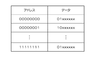
具体的に、このルックアップテーブルは図3に例示するように、N=8ビット長のビット列「00000000」が表すアドレスには、そのMSB(最上位ビット)に当該ビット列「00000000」の排他的論理和の演算結果である「0」を含み、その次のビットにこの演算結果の反転ビットである「1」を含んだデータ「01XXXXXX」(ここでXは不定でよい)が格納される。また、ビット列「00000001」が表すアドレスには、そのMSB(最上位ビット)に当該ビット列「00000001」の排他的論理和の演算結果である「1」を含み、次のビットにその反転ビットである「0」を含んだデータ「10XXXXXX」(Xは不定でよい)が格納される。
Specifically, as illustrated in FIG. 3, in the lookup table, an address represented by a bit string “00000000” having an N = 8 bit length includes an exclusive logic of the bit string “00000000” in its MSB (most significant bit). Data “01XXXXXXX” (here, X may be indefinite) including “0” that is the sum operation result and “1” that is the inverted bit of this operation result is stored in the next bit. The address represented by the bit string “00000001” includes “1” that is the result of the exclusive OR of the bit string “00000001” in its MSB (most significant bit), and the next bit is the inverted bit. Data “10XXXXXXX” (“X” may be indefinite) including “0” is stored.
この例では、出力部13は、外部から1ビットの信号の入力を受け入れる。そして出力部13は、メモリデバイス12が格納しているデータのうち、入力バッファ部11が出力するビット列が表すアドレスに格納されているデータを読み出し、外部から入力された1ビットの信号が「0」であるか「1」であるかにより、当該データのうち、上記論理演算結果またはその反転ビットのいずれかを選択的に出力する。本実施の形態の一例では、この出力部13は、外部から入力された1ビットの信号が「0」であるときには、メモリデバイスが格納しているデータのうち、入力バッファ部11が出力するビット列が表すアドレスに格納されているデータを読み出し、当該データのうちのMSBのビットを出力する。また出力部13は、外部から入力された1ビットの信号が「1」であるときには、メモリデバイスが格納しているデータのうち、入力バッファ部11が出力するビット列が表すアドレスに格納されているデータを読み出し、当該データのうちのMSBの次のビット(論理演算結果の反転ビットが格納されているビット)を出力する。
In this example, the output unit 13 accepts a 1-bit signal input from the outside. The output unit 13 reads the data stored in the address represented by the bit string output from the input buffer unit 11 among the data stored in the memory device 12, and the 1-bit signal input from the outside is “0”. "1" or "1", the logical operation result or its inverted bit is selectively output from the data. In the example of the present embodiment, the output unit 13 is a bit string output from the input buffer unit 11 among the data stored in the memory device when the 1-bit signal input from the outside is “0”. The data stored at the address indicated by is read, and the MSB bit of the data is output. Further, when the 1-bit signal input from the outside is “1”, the output unit 13 is stored in the address represented by the bit string output from the input buffer unit 11 among the data stored in the memory device. The data is read, and the next bit of the MSB of the data (the bit storing the inverted bit of the logical operation result) is output.
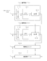
本実施の形態は基本的に以上の構成を備えており、次の例のように動作する。本実施の形態の以下の例では図4に例示するように、複数の論理演算ユニット10_1,10_2…10_nを備えるものとする。また、i番目の論理演算ユニット10_iの出力部13_iは、i-1番目の論理演算ユニット10_i-1の出力ビットを、外部からの入力として受け入れる。なお、先頭の論理演算ユニット10_1の出力部13_1は、外部からの入力を受けずに(あるいは外部からの入力を「0」に固定するなどして)、メモリデバイス12が格納しているデータのうち論理演算結果を表すビット(上述の例ではMSB)を出力することとする。
This embodiment basically has the above configuration and operates as in the following example. In the following example of the present embodiment, a plurality of logical operation units 10_1, 10_2,... 10_n are provided as illustrated in FIG. The output unit 13_i of the i-th logic operation unit 10_i accepts the output bit of the i-1th logic operation unit 10_i-1 as an input from the outside. Note that the output unit 13_1 of the first logical operation unit 10_1 does not receive an external input (or fixes the external input to “0”, for example), and stores the data stored in the memory device 12. Of these, a bit representing the logical operation result (MSB in the above example) is output.
また本実施の形態のこの例では、排他的論理和の計算の対象として8×n(メモリデバイス12のアドレスバス幅の整数n倍)ビット長のデータD(そのi番目のビットをbi(i=1,2,…8n)とする)の入力を受け入れる。そしてMSB側(あるいはLSB側)から順に8ビット(メモリデバイス12のアドレスバス幅)ずつ、それぞれ論理演算ユニット10_1,10_2…10_nのバッファ部11_1,11_2,…11_nに出力する。
In this example of the present embodiment, the data D (the i-th bit is represented by bi (i) as the object of the exclusive OR calculation, which is 8 × n (an integer n times the address bus width of the memory device 12). = 1, 2,..., 8n)). Then, 8 bits (address bus width of the memory device 12) are sequentially output from the MSB side (or LSB side) to the buffer units 11_1, 11_2,... 11_n of the logical operation units 10_1, 10_2,.
論理演算ユニット10_1の出力部13_1は、メモリデバイス12_1が格納しているデータのうち、入力バッファ11_1に入力された8ビット長のビット列(b1,b2,…b8)が表すアドレスに格納されているデータを読み出す。そして当該読み出したデータに含まれる論理演算結果(ここでは、入力された8ビット長のビット列の排他的論理和の演算結果とする)のビットを出力する。
The output unit 13_1 of the logical operation unit 10_1 is stored in the address represented by the 8-bit long bit string (b1, b2,..., B8) input to the input buffer 11_1 among the data stored in the memory device 12_1. Read data. Then, the bits of the logical operation result (here, the operation result of the exclusive OR of the input 8-bit length bit string) included in the read data are output.
次の論理演算ユニット10_2の出力部13_2は、メモリデバイス12_2が格納しているデータのうち、入力バッファ11_2に入力された8ビット長のビット列(b9,b10,…b16)が表すアドレスに格納されているデータを読み出す。またこの出力部13_2は、前段の論理演算ユニット10_1の出力部13_1が出力するビットに基づいて、当該読み出したデータに含まれる論理演算結果のビットまたはその反転ビットのいずれか一方を選択して出力する。具体的に出力部13_2は、出力部13_1が出力するビットが「0」であるときには、読み出したデータに含まれる論理演算結果を出力する。また出力部13_2は出力部13_1が出力するビットが「1」であるときには、論理演算結果の反転ビットを出力する。
The output unit 13_2 of the next logical operation unit 10_2 is stored at the address represented by the 8-bit long bit string (b9, b10,..., B16) input to the input buffer 11_2 among the data stored in the memory device 12_2. Read out data. The output unit 13_2 selects and outputs either the bit of the logical operation result included in the read data or its inverted bit based on the bit output from the output unit 13_1 of the preceding logical operation unit 10_1. To do. Specifically, the output unit 13_2 outputs a logical operation result included in the read data when the bit output from the output unit 13_1 is “0”. The output unit 13_2 outputs an inverted bit of the logical operation result when the bit output from the output unit 13_1 is “1”.
以下、i番目の論理演算ユニット10_iの出力部13_iは、メモリデバイス12_iが格納しているデータのうち、入力バッファ11_iに入力された8ビット長のビット列(b8(i-1)+1,b8(i-1)+2,…b8i)が表すアドレスに格納されているデータを読み出す。またこの出力部13_iは、前段の論理演算ユニット10_i-1の出力部13_i-1が出力するビットに基づいて、当該読み出したデータに含まれる論理演算結果のビットまたはその反転ビットのいずれか一方を選択して出力する。具体的に出力部13_iは、出力部13_i-1が出力するビットが「0」であるときには、読み出したデータに含まれる論理演算結果を出力する。また出力部13_iは出力部13_i-1が出力するビットが「1」であるときには、論理演算結果の反転ビットを出力する。
Hereinafter, the output unit 13_i of the i-th logical operation unit 10_i uses the 8-bit length bit string (b8 (i-1) +1, b8) input to the input buffer 11_i among the data stored in the memory device 12_i. Read the data stored at the address indicated by (i-1) +2,..., b8i). Further, the output unit 13_i outputs either the bit of the logical operation result included in the read data or its inverted bit based on the bit output from the output unit 13_i-1 of the preceding logical operation unit 10_i-1. Select and output. Specifically, the output unit 13_i outputs a logical operation result included in the read data when the bit output from the output unit 13_i-1 is “0”. The output unit 13_i outputs an inverted bit of the logical operation result when the bit output from the output unit 13_i-1 is “1”.
そしてn番目の論理演算ユニット10_nの出力部13_nは、メモリデバイス12_nが格納しているデータのうち、入力バッファ11_nに入力された8ビット長のビット列(b8(n-1)+1,b8(n-1)+2,…b8n)が表すアドレスに格納されているデータを読み出す。またこの出力部13_nは、前段の論理演算ユニット10_n-1の出力部13_n-1が出力するビットに基づいて、当該読み出したデータに含まれる論理演算結果のビットまたはその反転ビットのいずれか一方を選択して出力する。具体的に出力部13_nは、出力部13_n-1が出力するビットが「0」であるときには、読み出したデータに含まれる論理演算結果を出力する。また出力部13_nは出力部13_n-1が出力するビットが「1」であるときには、論理演算結果の反転ビットを出力する。
The output unit 13_n of the n-th logical operation unit 10_n includes an 8-bit length bit string (b8 (n-1) +1, b8 () input to the input buffer 11_n among the data stored in the memory device 12_n. n-1) +2,... b8n) reads data stored at the address indicated. The output unit 13_n outputs either the bit of the logical operation result included in the read data or its inverted bit based on the bit output from the output unit 13_n-1 of the preceding logical operation unit 10_n-1. Select and output. Specifically, the output unit 13_n outputs a logical operation result included in the read data when the bit output from the output unit 13_n−1 is “0”. The output unit 13_n outputs an inverted bit of the logical operation result when the bit output from the output unit 13_n-1 is “1”.
こうしてn番目の論理演算ユニット10_nの出力部13_nは、8×nビット長のデータDに含まれる各ビットの論理演算結果(ここでの例では排他的論理和)を出力することとなる。
Thus, the output unit 13_n of the nth logical operation unit 10_n outputs a logical operation result (exclusive OR in this example) of each bit included in the data D having a length of 8 × n bits.
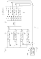
さらにここでは複数の論理演算ユニット10、つまりはメモリデバイス12を並列的に用いる例について述べたが、本実施の形態はこれに限られない。本実施の形態の別の例では、メモリデバイス12を時分割的に利用してもよい。この例に係る本発明の実施の形態に係る論理演算装置1は、図5に例示するように、n個のスリーステートバッファ部20と、メモリデバイス12と、クロック供給部25と、出力ユニット30とを含んで構成される。またスリーステートバッファ部20はそれぞれN(ここでの例ではN=8)個のスリーステートバッファ21を含み、出力ユニット30は、出力部31と、フリップフロップ回路部32と、スイッチ部33とを含む。ここで、既に説明したものと同様の構成をとるものについては同じ符号を付して説明を省略する。なお、この例ではメモリデバイス12には、図3に例示したデータが格納されているものとする。
Further, although an example in which a plurality of logical operation units 10, that is, memory devices 12 are used in parallel has been described here, the present embodiment is not limited to this. In another example of the present embodiment, the memory device 12 may be used in a time division manner. As illustrated in FIG. 5, the logical operation device 1 according to the embodiment of the present invention relating to this example includes n three-state buffer units 20, a memory device 12, a clock supply unit 25, and an output unit 30. It is comprised including. Each of the three-state buffer units 20 includes N (N = 8 in this example) three-state buffers 21, and the output unit 30 includes an output unit 31, a flip-flop circuit unit 32, and a switch unit 33. Including. Here, components having the same configurations as those already described are denoted by the same reference numerals and description thereof is omitted. In this example, it is assumed that the memory device 12 stores the data illustrated in FIG.
スリーステートバッファ21は、それぞれ入力端子Xと出力端子Yとゲート端子Gとを備える。このスリーステートバッファ21は、ゲート端子Gの入力が「0」である間、入力端子Xにどのような入力があったとしても、出力端子Yの状態をハイ・インピーダンス状態「Z」とする。出力端子Yがハイ・インピーダンスとなったスリーステートバッファ21は、当該出力端子Yの接続先からみると、絶縁された状態と同じ(接続が切離された状態)となる。
The three-state buffer 21 includes an input terminal X, an output terminal Y, and a gate terminal G, respectively. The three-state buffer 21 sets the state of the output terminal Y to the high impedance state “Z” regardless of what is input to the input terminal X while the input of the gate terminal G is “0”. When viewed from the connection destination of the output terminal Y, the three-state buffer 21 in which the output terminal Y has a high impedance is the same as an insulated state (a state in which the connection is disconnected).
本実施の形態のこの例では、8n個のスリーステートバッファ21が第1番目のスリーステートバッファ21_1から第8番目のスリーステートバッファ21_8までのグループ、第9番目のスリーステートバッファ21_9から第16番目のスリーステートバッファ21_16までのグループ…というように、8つずつのグループに分けられる。そして同じグループに属するスリーステートバッファ21のゲート端子Gには、クロック供給部25から同じ信号が入力される。この信号については後に述べる。また、i番目のスリーステートバッファ21_iの入力端子X_iには、論理演算の対象となる8×nビット長のデータDのMSB側(あるいはLSB側)から順に各ビットの値が入力される。
In this example of the present embodiment, 8n three-state buffers 21 are a group from the first three-state buffer 21_1 to the eighth three-state buffer 21_8, and from the ninth three-state buffer 21_9 to the sixteenth. The groups up to the three-state buffer 21_16 are divided into eight groups. The same signal is input from the clock supply unit 25 to the gate terminals G of the three-state buffers 21 belonging to the same group. This signal will be described later. Also, the value of each bit is input to the input terminal X_i of the i-th three-state buffer 21_i in order from the MSB side (or LSB side) of the data D of 8 × n bit length to be subjected to logical operation.
またi番目のスリーステートバッファ21_iの出力端子Y_iは、メモリデバイス12のアドレスバスのうち(i mod 8)番目のピンに接続される。ここで(i mod k)は、iをkで除したときの余りを意味する。
The output terminal Y_i of the i-th three-state buffer 21_i is connected to the (i (mod 8) -th pin of the address bus of the memory device 12. Here, (i mod k) means the remainder when i is divided by k.
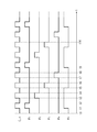
クロック供給部25は、図6に示すように、定期的に立ち上がりと立ち下りとを繰返すクロック信号CLKを生成してこれを出力する。またこのクロック供給部25は、n個(nは論理演算の対象となるビット数8nを、メモリデバイス12のアドレスバス幅である8で除した値)のサブクロック信号φi(i=1,2,…n)を生成する。図6には、n=4の場合のサブクロック信号φ1,φ2,φ3,φ4と、φ0とを例示している。
このサブクロック信号φiの立ち上がり、または立ち下りタイミングは次のようになる。すなわち、所定の時点(例えばt2)からj回目にクロック信号CLKが立ち上る際、i=(j mod n)+1のサブクロック信号φiが立ち上がり、j回目にクロック信号CLKが立ち下る際に、i=(j mod n)+1のサブクロック信号φiが立ち下るようにしておく。この際、i≠(j mod n)+1なるサブクロック信号φiはLの状態を維持するものとする。
例えば図6(n=4の例を表す)において、所定の時点であるt2の後、1回目にクロック信号CLKが立ち上る際(時点t3)、i=(1 mod 4)+1=2であるサブクロック信号φ2が立ち上がり、所定の時点であるt2の後、1回目にクロック信号CLKが立ち下る際(時点t4)、i=(1 mod 4)+1=2であるサブクロック信号φ2が立ち下る。
またクロック供給部25は次のようなサブクロック信号φ0を生成する。すなわち、このφ0は、所定の時点からj回目にクロック信号CLKが立ち上がる際に(j mod n)=0であれば立ち上がり、その後のクロック信号CLKのn/2+1回目または(n-1)/2+1回目の立ち下り時など、その後、クロック信号CLKがn回目に立ち下るまでに立ち下るようにする。
具体的に図6の例では、所定の時点であるt2の後、4回目のクロック信号CLKの立ち上がり時(時点t9)に、(4 mod 4)=0となるので、クロック供給部25は、この時点でサブクロック信号φ0が立ち上るように制御する。また、クロック供給部25は、その後(時点t9の後)、クロック信号CLKのn/2+1回目または(n-1)/2+1回目の立ち下り時(ここではn/2+1=3回目とする)の立ち下り時(時点t14)までにサブクロック信号φ0が立ち下るように制御する。図6の例では時点t9からn/2+1回目、つまり3回目の立ち下り時の直前のクロック信号CLKの立ち上がりタイミングにてサブクロック信号φ0が立ち下るように制御した例を示している。 As shown in FIG. 6, theclock supply unit 25 generates and outputs a clock signal CLK that periodically repeats rising and falling. The clock supply unit 25 also includes n sub-clock signals φi (i = 1, 2), where n is a value obtained by dividing the number of bits 8n to be subjected to logic operation by 8 which is the address bus width of the memory device 12. ,... N). FIG. 6 illustrates subclock signals φ1, φ2, φ3, φ4, and φ0 in the case of n = 4.
The rise or fall timing of the sub clock signal φi is as follows. That is, when the clock signal CLK rises j times from a predetermined time (for example, t2), the i = (j mod n) +1 subclock signal φi rises, and when the clock signal CLK falls j times, i = The subclock signal φi of (j mod n) +1 is set to fall. At this time, it is assumed that the subclock signal φi where i ≠ (j mod n) +1 maintains the L state.
For example, in FIG. 6 (representing an example of n = 4), after the predetermined time t2, when the clock signal CLK rises for the first time (time t3), i = (1 mod 4) + 1 = 2 When the clock signal φ2 rises and the clock signal CLK falls for the first time (time t4) after the predetermined time t2, the sub-clock signal φ2 with i = (1 mod 4) + 1 = 2 falls.
Theclock supply unit 25 generates the following subclock signal φ0. That is, φ0 rises when the clock signal CLK rises j times from a predetermined time if (j mod n) = 0, and then rises n / 2 + 1 times or (n−1) / 2 + 1 of the subsequent clock signal CLK. Thereafter, the clock signal CLK falls until the nth fall, such as at the time of the fall.
Specifically, in the example of FIG. 6, since (4 mod 4) = 0 at the rise of the fourth clock signal CLK (time t9) after t2 which is a predetermined time, theclock supply unit 25 At this time, the sub-clock signal φ0 is controlled to rise. Further, the clock supply unit 25 thereafter (after time t9) at the falling edge of the clock signal CLK at the (n + 1) th or (n-1) / 2 + 1th time (here, n / 2 + 1 = third time). Control is performed so that the sub-clock signal φ0 falls before the fall (time t14). The example of FIG. 6 shows an example in which the sub-clock signal φ0 is controlled to fall at the rising timing of the clock signal CLK immediately before the time of n / 2 + 1 times from the time point t9, that is, the third falling time.
このサブクロック信号φiの立ち上がり、または立ち下りタイミングは次のようになる。すなわち、所定の時点(例えばt2)からj回目にクロック信号CLKが立ち上る際、i=(j mod n)+1のサブクロック信号φiが立ち上がり、j回目にクロック信号CLKが立ち下る際に、i=(j mod n)+1のサブクロック信号φiが立ち下るようにしておく。この際、i≠(j mod n)+1なるサブクロック信号φiはLの状態を維持するものとする。
例えば図6(n=4の例を表す)において、所定の時点であるt2の後、1回目にクロック信号CLKが立ち上る際(時点t3)、i=(1 mod 4)+1=2であるサブクロック信号φ2が立ち上がり、所定の時点であるt2の後、1回目にクロック信号CLKが立ち下る際(時点t4)、i=(1 mod 4)+1=2であるサブクロック信号φ2が立ち下る。
またクロック供給部25は次のようなサブクロック信号φ0を生成する。すなわち、このφ0は、所定の時点からj回目にクロック信号CLKが立ち上がる際に(j mod n)=0であれば立ち上がり、その後のクロック信号CLKのn/2+1回目または(n-1)/2+1回目の立ち下り時など、その後、クロック信号CLKがn回目に立ち下るまでに立ち下るようにする。
具体的に図6の例では、所定の時点であるt2の後、4回目のクロック信号CLKの立ち上がり時(時点t9)に、(4 mod 4)=0となるので、クロック供給部25は、この時点でサブクロック信号φ0が立ち上るように制御する。また、クロック供給部25は、その後(時点t9の後)、クロック信号CLKのn/2+1回目または(n-1)/2+1回目の立ち下り時(ここではn/2+1=3回目とする)の立ち下り時(時点t14)までにサブクロック信号φ0が立ち下るように制御する。図6の例では時点t9からn/2+1回目、つまり3回目の立ち下り時の直前のクロック信号CLKの立ち上がりタイミングにてサブクロック信号φ0が立ち下るように制御した例を示している。 As shown in FIG. 6, the
The rise or fall timing of the sub clock signal φi is as follows. That is, when the clock signal CLK rises j times from a predetermined time (for example, t2), the i = (j mod n) +1 subclock signal φi rises, and when the clock signal CLK falls j times, i = The subclock signal φi of (j mod n) +1 is set to fall. At this time, it is assumed that the subclock signal φi where i ≠ (j mod n) +1 maintains the L state.
For example, in FIG. 6 (representing an example of n = 4), after the predetermined time t2, when the clock signal CLK rises for the first time (time t3), i = (1 mod 4) + 1 = 2 When the clock signal φ2 rises and the clock signal CLK falls for the first time (time t4) after the predetermined time t2, the sub-clock signal φ2 with i = (1 mod 4) + 1 = 2 falls.
The
Specifically, in the example of FIG. 6, since (4 mod 4) = 0 at the rise of the fourth clock signal CLK (time t9) after t2 which is a predetermined time, the
ここでクロック供給部25は、サブクロック信号φ1を第1番目のスリーステートバッファ21_1から第8番目のスリーステートバッファ21_8に供給し、サブクロック信号φ2を第9番目のスリーステートバッファ21_9から第16番目のスリーステートバッファ21_16に供給し…というように、サブクロックφiを、8つのスリーステートバッファ21_([i/8]+1)にそれぞれ供給する。ここで[*]は*を超えない最大の整数を意味するものとする。
Here, the clock supply unit 25 supplies the subclock signal φ1 from the first three-state buffer 21_1 to the eighth three-state buffer 21_8, and the subclock signal φ2 from the ninth three-state buffer 21_9 to the sixteenth. The sub clock φi is supplied to each of the eight three-state buffers 21 _ ([i / 8] +1). Here, [*] means the maximum integer not exceeding *.
これらスリーステートバッファ21と、クロック供給部25との動作により、M(Mは、M>Nなる整数)ビット長のビット列の入力を受けて、当該ビット列からNビットのビット列を抽出して、当該抽出したNビットのビット列を時分割的にメモリデバイス12に対して出力する分割手段が実現される。
The operation of the three-state buffer 21 and the clock supply unit 25 receives an input of a bit string of M (M is an integer of M> N) bit length, extracts an N-bit bit string from the bit string, Dividing means for outputting the extracted N-bit bit string to the memory device 12 in a time division manner is realized.
出力ユニット30の出力部31は、クロック供給部25から入力されるクロック信号CLKが立ち下るタイミングであり、かつ、サブクロック信号φn(nは論理演算の対象となるビット数8nを、メモリデバイス12のアドレスバス幅である8で除した値)が立ち下らないタイミングにおいて、フリップフロップ回路部32が出力する1ビットの信号の入力を受け入れてバッファ(不図示)に保持する。そして出力部31は、次にクロック信号CLKが立ち上るタイミングでメモリデバイス12が格納しているデータのうち、スリーステートバッファ21が出力するビット列が表すアドレスに格納されているデータを読み出す。出力部31は、バッファに保持した1ビットの信号が「0」であるか「1」であるかにより、当該読み出したデータのうち、上記論理演算結果またはその反転ビットのいずれかを選択的に出力する。
The output unit 31 of the output unit 30 is the timing at which the clock signal CLK input from the clock supply unit 25 falls, and the sub clock signal φn (n is the number of bits 8n to be subjected to a logical operation, and the memory device 12 At a timing at which the address bus width divided by 8) does not fall, a 1-bit signal output from the flip-flop circuit unit 32 is received and held in a buffer (not shown). The output unit 31 reads data stored at an address represented by the bit string output from the three-state buffer 21 among the data stored in the memory device 12 at the next timing when the clock signal CLK rises. The output unit 31 selectively selects either the logical operation result or its inverted bit from the read data depending on whether the 1-bit signal held in the buffer is “0” or “1”. Output.
本実施の形態の一例では、この出力部31は、バッファに保持したビットが「0」であるときには、メモリデバイス12から読み出したデータのうちMSBのビット(論理演算結果)をスイッチ部33に出力する。またこの出力部31は、バッファに保持したビットが「1」であるときには、メモリデバイス12から読み出したデータのうちMSBの次のビット(論理演算結果の反転ビットが格納されているビット)をスイッチ部33に出力する。出力部31は、この出力を、次にクロック信号CLKが立ち下るまで継続する。
In the example of the present embodiment, the output unit 31 outputs the MSB bit (logical operation result) of the data read from the memory device 12 to the switch unit 33 when the bit held in the buffer is “0”. To do. In addition, when the bit held in the buffer is “1”, the output unit 31 switches the next bit of the MSB (bit storing the inverted bit of the logical operation result) in the data read from the memory device 12. To the unit 33. The output unit 31 continues this output until the clock signal CLK falls next time.
またこの出力部31は、後に説明するスイッチ部33を制御する。具体的に出力部31は、クロック供給部25が出力するサブクロック信号φn(nは論理演算の対象となるビット数8nを、メモリデバイス12のアドレスバス幅である8で除した値)が立ち上がるタイミングで、後に説明するスイッチ部33の出力先を、外部への出力に設定する。そして次にクロック供給部25が出力するクロック信号CLKが立ち上るタイミングでスイッチ部33の出力先をフリップフロップ回路部32に設定する。
The output unit 31 controls a switch unit 33 which will be described later. Specifically, the output unit 31 rises a sub clock signal φn output from the clock supply unit 25 (n is a value obtained by dividing the number of bits 8n to be subjected to logical operation by 8 which is the address bus width of the memory device 12). At the timing, the output destination of the switch unit 33 described later is set to output to the outside. Then, the output destination of the switch unit 33 is set in the flip-flop circuit unit 32 at the timing when the clock signal CLK output from the clock supply unit 25 rises.
さらに出力部31は、クロック供給部25が出力するサブクロック信号φnが立ち下るタイミングでは、フリップフロップ回路部32の出力に関わらず、バッファに「0」のビットを保持する。この動作を、以下では、出力部のリセット動作と呼ぶ。
Further, the output unit 31 holds a bit of “0” in the buffer regardless of the output of the flip-flop circuit unit 32 at the timing when the sub clock signal φn output from the clock supply unit 25 falls. This operation is hereinafter referred to as an output unit reset operation.
フリップフロップ回路部32は、例えばD型のフリップフロップ回路を含んで構成される。このフリップフロップ回路24では具体的にD端子(入力端子)が出力部31の出力を受け入れる。また、C端子(クロック端子)は、クロック供給部25からクロック信号CLKの入力を受ける。そしてこのフリップフロップ回路部32は、クロック信号CLKが立ち上るタイミングで、入力端子であるD端子に入力されるビットを保持して出力端子Qに当該ビットの信号を出力する。この出力は、クロック信号CLKが立ち下るタイミングでも継続される。またこの出力端子Qから出力されるビットが、フリップフロップ回路部32からの出力として出力部31に入力される。
The flip-flop circuit unit 32 includes, for example, a D-type flip-flop circuit. Specifically, in the flip-flop circuit 24, the D terminal (input terminal) receives the output of the output unit 31. The C terminal (clock terminal) receives the clock signal CLK from the clock supply unit 25. The flip-flop circuit unit 32 holds a bit input to the D terminal, which is an input terminal, and outputs a signal of the bit to the output terminal Q at the timing when the clock signal CLK rises. This output is continued even when the clock signal CLK falls. A bit output from the output terminal Q is input to the output unit 31 as an output from the flip-flop circuit unit 32.
スイッチ部33は、出力部31からの制御を受け入れて、出力部31から入力された1ビットの情報を、フリップフロップ回路部32または外部のいずれかに対して選択的に出力する。
The switch unit 33 accepts control from the output unit 31 and selectively outputs the 1-bit information input from the output unit 31 to either the flip-flop circuit unit 32 or the outside.
本実施の形態のこの例に係る論理演算装置1の動作を次に説明する。ここでは例えば論理演算としての排他的論理和の計算の対象としてM=N×n(メモリデバイス12のアドレスバス幅Nの整数n倍)ビット長のデータD(そのi番目のビットをbi(i=1,2,…N×n)とする)の入力を受け入れる。そしてMSB側(あるいはLSB側)から順にi番目のビットを、それぞれ第i番目のスリーステートバッファ21_iに入力する。
The operation of the logical operation device 1 according to this example of the present embodiment will be described next. Here, for example, M = N × n (an integer n times the address bus width N of the memory device 12) bit length data D (its i-th bit is expressed as bi (i = 1, 2,... N × n)). Then, the i-th bit is input to the i-th three-state buffer 21 — i in order from the MSB side (or LSB side).
そして論理演算装置1は次のように動作する。すなわち、出力部のリセット動作が行われたとき(図6の時刻t0)に、出力部31は「0」のビットをバッファに保持する。次にクロック供給部25の出力するクロック信号CLKが立ち上るタイミング(図6の時刻t1)において、スリーステートバッファ21_1から21_8が、入力されたビットb1,b2,…b8を、メモリデバイス12のアドレスバスに供給する。
And the logical operation device 1 operates as follows. That is, when the reset operation of the output unit is performed (time t0 in FIG. 6), the output unit 31 holds the bit “0” in the buffer. Next, at the timing when the clock signal CLK output from the clock supply unit 25 rises (time t1 in FIG. 6), the three-state buffers 21_1 to 21_8 use the input bits b1, b2,. To supply.
出力部31は、メモリデバイス12が格納しているデータのうち、スリーステートバッファ21_1から21_8が出力するビット列が表すアドレスに格納されているデータを読み出す。このとき、出力部31のバッファは「0」のビットを保持しているので、この出力部31は、メモリデバイス12から読み出したデータのうちMSBのビット(論理演算結果)を第1回目の演算結果R1として出力する。この出力R1はスイッチ部33を介してフリップフロップ回路部32に出力されて、フリップフロップ回路部32において保持される。
The output unit 31 reads the data stored in the address represented by the bit string output from the three-state buffers 21_1 to 21_8 among the data stored in the memory device 12. At this time, since the buffer of the output unit 31 holds the bit “0”, the output unit 31 calculates the MSB bit (logical operation result) of the data read from the memory device 12 in the first operation. Output as the result R1. The output R 1 is output to the flip-flop circuit unit 32 via the switch unit 33 and is held in the flip-flop circuit unit 32.
次にクロック供給部25の出力するクロック信号CLKが立ち下るタイミング(図6の時刻t2)になると、スリーステートバッファ21_1から21_8の出力はハイ・インピーダンスとなる。そして出力部31はフリップフロップ回路部32から前回の演算結果R1を受け入れてバッファに保持する。
Next, when the clock signal CLK output from the clock supply unit 25 falls (time t2 in FIG. 6), the outputs of the three-state buffers 21_1 to 21_8 become high impedance. The output unit 31 receives the previous calculation result R1 from the flip-flop circuit unit 32 and holds it in the buffer.
次にクロック供給部25の出力するクロック信号CLKが立ち上るタイミング(図6の時刻t3)では、スリーステートバッファ21_9から21_16が、入力されたビットb9,b10,…b16を、メモリデバイス12のアドレスバスに供給する。
Next, at the timing when the clock signal CLK output from the clock supply unit 25 rises (time t3 in FIG. 6), the three-state buffers 21_9 to 21_16 transfer the input bits b9, b10,... B16 to the address bus of the memory device 12. To supply.
出力部31は、メモリデバイス12が格納しているデータのうち、スリーステートバッファ21_9から21_16が出力するビット列が表すアドレスに格納されているデータを読み出す。そして出力部31は、そのバッファが「0」のビットを保持しているとき(演算結果R1が「0」であったとき)には、メモリデバイス12から読み出したデータのうちMSBのビット(論理演算結果)を第2回目の演算結果R2として出力する。また出力部31は、そのバッファが「1」のビットを保持しているとき(演算結果R1が「1」であったとき)には、メモリデバイス12から読み出したデータのうちMSBの次のビット(論理演算結果の反転ビット)を第2回目の演算結果R2として出力する。この出力R2はスイッチ部33を介してフリップフロップ回路部32に出力されて、フリップフロップ回路部32において保持される。
The output unit 31 reads the data stored in the address represented by the bit string output from the three-state buffers 21_9 to 21_16 among the data stored in the memory device 12. When the buffer holds a bit of “0” (when the operation result R 1 is “0”), the output unit 31 outputs the MSB bit (logic) of the data read from the memory device 12. The calculation result is output as the second calculation result R2. In addition, when the buffer holds the bit “1” (when the operation result R1 is “1”), the output unit 31 outputs the next bit of the MSB in the data read from the memory device 12. (The inverted bit of the logical operation result) is output as the second operation result R2. The output R 2 is output to the flip-flop circuit unit 32 via the switch unit 33 and is held in the flip-flop circuit unit 32.
以下同様に動作し、クロック供給部25の出力するサブクロック信号φnが立ち上るタイミングにおいて出力部31は、スイッチ部33の出力先を外部への出力に設定する。またこのとき出力部31は、メモリデバイス12が格納しているデータのうち、スリーステートバッファ21_(8×(n-1)+1)から21_(8n)が出力するビット列が表すアドレスに格納されているデータを読み出す。そして出力部31は、そのバッファが「0」のビットを保持しているとき(演算結果Rn-1が「0」であったとき)には、メモリデバイス12から読み出したデータのうちMSBのビット(論理演算結果)を演算結果Rとして出力する。また出力部31は、そのバッファが「1」のビットを保持しているとき(演算結果Rn-1が「1」であったとき)には、メモリデバイス12から読み出したデータのうちMSBの次のビット(論理演算結果の反転ビット)を演算結果Rとして出力する。この出力は、スイッチ部33を介して外部に供給される。
Hereinafter, the same operation is performed, and the output unit 31 sets the output destination of the switch unit 33 to output to the outside at the timing when the sub clock signal φn output from the clock supply unit 25 rises. At this time, the output unit 31 stores the data stored in the memory device 12 at the address indicated by the bit string output from the three-state buffers 21_ (8 × (n−1) +1) to 21_ (8n). Read data. When the buffer holds a bit of “0” (when the calculation result Rn−1 is “0”), the output unit 31 stores the MSB bit in the data read from the memory device 12. The (logical operation result) is output as the operation result R. In addition, when the buffer holds a bit of “1” (when the calculation result Rn−1 is “1”), the output unit 31 outputs the next MSB of the data read from the memory device 12. (The inverted bit of the logical operation result) is output as the operation result R. This output is supplied to the outside via the switch unit 33.
出力部31は、次にクロック信号CLKが立ち下るタイミングで出力部のリセット動作を行い、さらに次にクロック信号CLKが立ち上るタイミングではスイッチ部33の出力先をフリップフロップ回路部32に設定する。
The output unit 31 performs the reset operation of the output unit at the next timing when the clock signal CLK falls, and further sets the output destination of the switch unit 33 in the flip-flop circuit unit 32 at the next timing when the clock signal CLK rises.
このように、本実施の形態のこの例では、出力部31が、時分割的にNビットのビット列が出力されるタイミングにおいて、前回出力したビットを用いて、メモリデバイスにアクセスして取り出したビット間の論理演算結果と、その反転ビットとの一方を選択的に出力する手段として機能している。
As described above, in this example of the embodiment, the output unit 31 accesses the memory device using the previously output bit at the timing when the N-bit bit string is output in a time division manner. It functions as a means for selectively outputting one of the logical operation result between them and the inverted bit.
こうしてn回目には出力部31は、8×nビット長のデータDに含まれる各ビットの論理演算結果(ここでの例では排他的論理和)を演算結果Rとして出力することとなる。
Thus, at the n-th time, the output unit 31 outputs the logical operation result (exclusive OR in this example) of each bit included in the data D having a length of 8 × n bits as the operation result R.
さらにこのように時分割的に演算を行う場合の出力ユニットの例は、この例に限られない。すなわちメモリデバイス12の各アドレスに格納可能なデータは8ビットであるため、このビット幅を活用して次のように構成することも可能である。
Furthermore, the example of the output unit in the case of performing the operation in a time division manner is not limited to this example. That is, since the data that can be stored in each address of the memory device 12 is 8 bits, it is possible to make the following configuration by utilizing this bit width.
本実施の形態のさらに別の例に係る論理演算装置1は、図7に例示するように、8×n個(ここではメモリデバイス12のアドレスバス幅N=8としている)のスリーステートバッファ21(図5に例示したものと同様、8個ずつでスリーステートバッファ部20を構成する)と、メモリデバイス12と、クロック供給部25と、出力ユニット40とを含んで構成される。また出力ユニット40は、4つ(メモリデバイス12のデータバス幅Lの1/2)のセレクタ部41a,b,c,dを含んで構成されている。ここで、既に説明したものと同様の構成をとるものについては同じ符号を付して説明を省略する。
As illustrated in FIG. 7, the logical operation device 1 according to still another example of the present embodiment includes 8 × n three-state buffers 21 (here, the address bus width N of the memory device 12 is 8). (Similar to the example illustrated in FIG. 5, the three-state buffer unit 20 is configured with eight units each), the memory device 12, the clock supply unit 25, and the output unit 40. The output unit 40 includes four selector units 41a, b, c, and d (1/2 of the data bus width L of the memory device 12). Here, components having the same configurations as those already described are denoted by the same reference numerals and description thereof is omitted.
またこの例におけるメモリデバイス12には、図8に例示するように、8ビット長のアドレスA(ビット列a1,a2,…a8で表される)が示す位置に、MSB側から、ビット列a1,a2,…a8に基づく論理演算結果と、その反転ビットとの組が繰返し配される。つまりこの例では、各アドレスの位置に格納されるデータの奇数ビット目にはそれぞれ論理演算結果が格納され、偶数ビット目には、奇数ビット目にあるビットの反転ビットが格納される。
Further, in the memory device 12 in this example, as illustrated in FIG. 8, the bit string a1, a2 from the MSB side at the position indicated by the 8-bit long address A (represented by the bit string a1, a2,... A8). ,... A set of a logical operation result based on a8 and its inverted bit are repeatedly arranged. That is, in this example, the logical operation result is stored in the odd-numbered bit of the data stored at the position of each address, and the inverted bit of the bit in the odd-numbered bit is stored in the even-numbered bit.
出力ユニット40のセレクタ部41aには、メモリデバイス12のデータバスのうち、MSBであるd1と、MSBの次のビットであるd2との各信号線が接続される。またこのセレクタ部41aは、外部から入力される1ビットの信号を受け入れる。
The selector unit 41a of the output unit 40 is connected to signal lines of d1 which is the MSB and d2 which is the next bit of the MSB in the data bus of the memory device 12. The selector unit 41a accepts a 1-bit signal input from the outside.
そしてセレクタ部41aは、クロック供給部25から入力されるサブクロック信号φ1が立ち上がるタイミングで、メモリデバイス12が格納しているデータのうち、スリーステートバッファ21が出力するビット列が表すアドレスに格納されているデータを読み出してラッチする。このセレクタ部41aは、外部から受け入れた1ビットの信号が「0」であるか「1」であるかにより、当該読み出したデータのうち、上記論理演算結果を表すMSBの1ビット、またはその反転ビットを表すMSBの次の1ビットのいずれかを選択的にラッチして出力する。
The selector unit 41a stores the data stored in the memory device 12 at the address represented by the bit string output from the three-state buffer 21 at the timing when the sub clock signal φ1 input from the clock supply unit 25 rises. Read and latch the data. The selector unit 41a selects one bit of the MSB representing the logical operation result or the inverse of the read data depending on whether the 1-bit signal received from the outside is “0” or “1”. Any one bit of the next MSB representing the bit is selectively latched and output.
ここでの例では、セレクタ部41aは、外部から受け入れたビットが「0」であるときには、メモリデバイス12から読み出したデータのうちMSBのビット(信号線d1が出力する論理演算結果)を選択してラッチし、出力する。またこのセレクタ部41aは、外部から受け入れたビットが「1」であるときには、メモリデバイス12から読み出したデータのうちMSBの次のビット(論理演算結果の反転ビットを表す信号線d2の出力)を選択してラッチし、出力する。
In this example, when the bit received from the outside is “0”, the selector unit 41 a selects the MSB bit (the logical operation result output by the signal line d 1) from the data read from the memory device 12. Latch and output. In addition, when the bit received from the outside is “1”, the selector unit 41a outputs the bit next to the MSB (output of the signal line d2 representing the inverted bit of the logical operation result) in the data read from the memory device 12. Select, latch, and output.
またセレクタ部41bには、メモリデバイス12のデータバスのうち、MSB側のd3と、その次のビットであるd4との各信号線が接続される。またこのセレクタ部41bは、セレクタ部41aが出力する1ビットの信号を受け入れる。
Also, the selector unit 41b is connected to each signal line of d3 on the MSB side of the data bus of the memory device 12 and d4 which is the next bit. The selector unit 41b accepts a 1-bit signal output from the selector unit 41a.
そしてセレクタ部41bは、クロック供給部25から入力されるサブクロック信号φ2が立ち上がるタイミングで、メモリデバイス12が格納しているデータのうち、スリーステートバッファ21が出力するビット列が表すアドレスに格納されているデータを読み出してラッチする。このセレクタ部41bは、セレクタ部41aから受け入れた1ビットの信号が「0」であるか「1」であるかにより、当該読み出したデータのうち、上記論理演算結果を表すMSB側の1ビット、またはその反転ビットを表すその次の1ビットのいずれかを選択的にラッチして出力する。
The selector unit 41b stores the data stored in the memory device 12 at the address represented by the bit string output from the three-state buffer 21 at the timing when the sub clock signal φ2 input from the clock supply unit 25 rises. Read and latch the data. Depending on whether the 1-bit signal received from the selector unit 41a is “0” or “1”, the selector unit 41b has 1 bit on the MSB side representing the logical operation result among the read data, Alternatively, one of the next 1 bits representing the inverted bit is selectively latched and output.
ここでの例では、セレクタ部41bは、セレクタ部41aから受け入れたビットが「0」であるときには、メモリデバイス12から読み出したデータのうちMSB側のビット(信号線d3が出力する論理演算結果)を選択してラッチし、出力する。またこのセレクタ部41bは、セレクタ部41aから受け入れたビットが「1」であるときには、メモリデバイス12から読み出したデータのうち上記信号線d3の次の信号線d4の表すビット(論理演算結果の反転ビットを表す)を選択してラッチし、出力する。
In this example, when the bit received from the selector unit 41a is “0”, the selector unit 41b is the MSB side bit (the logical operation result output from the signal line d3) of the data read from the memory device 12. Is selected, latched, and output. When the bit received from the selector unit 41a is “1”, the selector unit 41b represents a bit (inverted logical operation result) of the data read from the memory device 12 and represented by the signal line d4 next to the signal line d3. (Represents bit) is selected, latched, and output.
セレクタ部41cには、メモリデバイス12のデータバスのうち、MSB側のd5と、その次のビットであるd6との各信号線が接続される。またこのセレクタ部41cは、セレクタ部41bが出力する1ビットの信号を受け入れる。
The selector unit 41c is connected to each signal line of d5 on the MSB side of the data bus of the memory device 12 and d6 which is the next bit. The selector unit 41c accepts a 1-bit signal output from the selector unit 41b.
そしてセレクタ部41cは、クロック供給部25から入力されるサブクロック信号φ3が立ち上がるタイミングで、メモリデバイス12が格納しているデータのうち、スリーステートバッファ21が出力するビット列が表すアドレスに格納されているデータを読み出してラッチする。ここでの例におけるセレクタ部41cはセレクタ部41bから受け入れたビットが「0」であるときには、メモリデバイス12から読み出したデータのうちMSB側のビット(信号線d5が出力する論理演算結果)を選択してラッチし、出力する。またこのセレクタ部41cは、セレクタ部41bから受け入れたビットが「1」であるときには、メモリデバイス12から読み出したデータのうち上記信号d5の次の信号線d6の表すビット(論理演算結果の反転ビットを表す)を選択してラッチし、出力する。
The selector unit 41c is stored at the address represented by the bit string output from the three-state buffer 21 among the data stored in the memory device 12 at the timing when the sub clock signal φ3 input from the clock supply unit 25 rises. Read and latch the data. In this example, when the bit received from the selector unit 41b is “0”, the selector unit 41c selects the MSB side bit (the logical operation result output by the signal line d5) from the data read from the memory device 12. To latch and output. In addition, when the bit received from the selector unit 41b is “1”, the selector unit 41c has a bit (inverted bit of the logical operation result) represented by the signal line d6 next to the signal d5 in the data read from the memory device 12. Is selected, latched, and output.
さらにセレクタ部41dには、メモリデバイス12のデータバスのうち、MSB側のd7と、その次のビットであるd8との各信号線が接続される。またこのセレクタ部41dは、セレクタ部41cが出力する1ビットの信号を受け入れる。
Further, each signal line of d7 on the MSB side and d8 which is the next bit in the data bus of the memory device 12 is connected to the selector unit 41d. The selector unit 41d accepts a 1-bit signal output from the selector unit 41c.
そしてセレクタ部41dは、クロック供給部25から入力されるサブクロック信号φ4が立ち上がるタイミングで、メモリデバイス12が格納しているデータのうち、スリーステートバッファ21が出力するビット列が表すアドレスに格納されているデータを読み出してラッチする。ここでの例におけるセレクタ部41dはセレクタ部41cから受け入れたビットが「0」であるときには、メモリデバイス12から読み出したデータのうちMSB側のビット(信号線d7が出力する論理演算結果)を選択してラッチし、出力する。またこのセレクタ部41cは、セレクタ部41bから受け入れたビットが「1」であるときには、メモリデバイス12から読み出したデータのうち上記信号d7の次の信号線d8の表すビット(論理演算結果の反転ビットを表す)を選択してラッチし、出力する。このセレクタ部41dの出力は、外部に出力される。
The selector unit 41d is stored at the address represented by the bit string output from the three-state buffer 21 among the data stored in the memory device 12 at the timing when the sub clock signal φ4 input from the clock supply unit 25 rises. Read and latch the data. In this example, when the bit received from the selector unit 41c is “0”, the selector unit 41d selects the MSB side bit (the logical operation result output by the signal line d7) from the data read from the memory device 12. To latch and output. In addition, when the bit received from the selector unit 41b is “1”, the selector unit 41c has a bit (inverted bit of the logical operation result) represented by the signal line d8 next to the signal d7 in the data read from the memory device 12. Is selected, latched, and output. The output of the selector unit 41d is output to the outside.
本実施の形態のこの例に係る論理演算装置1の動作を次に説明する。ここでは例えば論理演算としての排他的論理和の計算の対象としてM=N×n(メモリデバイス12のアドレスバス幅Nの整数n倍)ビット長のデータD(そのi番目のビットをbi(i=1,2,…N×n)とする)の入力を受け入れる。そしてMSB側(あるいはLSB側)から順にi番目のビットを、それぞれ第i番目のスリーステートバッファ21_iに入力する。
The operation of the logical operation device 1 according to this example of the present embodiment will be described next. Here, for example, M = N × n (an integer n times the address bus width N of the memory device 12) bit length data D (its i-th bit is expressed as bi (i = 1, 2,... N × n)). Then, the i-th bit is input to the i-th three-state buffer 21 — i in order from the MSB side (or LSB side).
そして論理演算装置1は次のように動作する。セレクタ部41dの出力があった後(図6の時刻t0)、次にクロック供給部25の出力するクロック信号CLK及びサブクロック信号φ1が立ち上るタイミング(図6の時刻t1)において、スリーステートバッファ21_1から21_8が、入力されたビットb1,b2,…b8を、メモリデバイス12のアドレスバスに供給する。
And the logical operation device 1 operates as follows. After the output of the selector unit 41d (time t0 in FIG. 6), the three-state buffer 21_1 at the next timing (time t1 in FIG. 6) at which the clock signal CLK and the sub clock signal φ1 output from the clock supply unit 25 rise. 21_8 supply the input bits b1, b2,..., B8 to the address bus of the memory device 12.
このとき、出力ユニット40のセレクタ部41aが、メモリデバイス12が格納しているデータのうち、スリーステートバッファ21_1から21_8が出力するビット列が表すアドレスに格納されているデータを読み出す。なお、ここでセレクタ部41aには外部から「0」の信号が入力されているものとする。セレクタ部41aは、ラッチを備え、このラッチがサブクロック信号φ1の立ち上るタイミング(図6の時刻t1)においてメモリデバイス12から読み出したデータのうちMSBのビット(データバスの信号線d1を介して出力されるデータ、つまり論理演算結果)を演算結果R1としてラッチし、出力する。この出力R1はセレクタ部41bに出力される。
At this time, the selector unit 41a of the output unit 40 reads the data stored in the address represented by the bit string output from the three-state buffers 21_1 to 21_8 among the data stored in the memory device 12. Here, it is assumed that a “0” signal is input to the selector unit 41a from the outside. The selector unit 41a includes a latch, and the MSB bit (data bus signal line d1) is output from the data read from the memory device 12 at a timing when the sub clock signal φ1 rises (time t1 in FIG. 6). Data, that is, a logical operation result) is latched and output as an operation result R1. The output R1 is output to the selector unit 41b.
セレクタ部41bは、この出力R1を受け入れておく。次にクロック供給部25の出力するクロック信号CLKと、サブクロック信号φ2とが立ち上るタイミング(図6の時刻t3)において、スリーステートバッファ21_9から21_16が、入力されたビットb9,b10,…b16を、メモリデバイス12のアドレスバスに供給する。
The selector unit 41b accepts this output R1. Next, at the timing when the clock signal CLK output from the clock supply unit 25 and the sub clock signal φ2 rise (time t3 in FIG. 6), the three-state buffers 21_9 to 21_16 store the input bits b9, b10,. To the address bus of the memory device 12.
そしてセレクタ部41bは、メモリデバイス12が格納しているデータのうち、スリーステートバッファ21_9から21_16が出力するビット列が表すアドレスに格納されているデータを読み出す。そしてセレクタ部41bは、セレクタ部41aから入力されたビットが「0」であるとき(演算結果R1が「0」であったとき)には、メモリデバイス12から読み出したデータのうちMSB側のビット(データバス上、d3の信号線の出力、つまり論理演算結果)を演算結果R2として、サブクロック信号φ2が立ち上るタイミング(図6の時刻t3)においてラッチし、出力する。またこのセレクタ部41bは、セレクタ部41aから入力されたビットが「1」であるとき(演算結果R1が「1」であったとき)には、メモリデバイス12から読み出したデータのうちd4の信号線の出力(論理演算結果の反転ビット)を演算結果R2として、サブクロック信号φ2が立ち上るタイミング(図6の時刻t3)においてラッチし、出力する。この出力R2は、セレクタ部41cによって受け入れられる。
The selector unit 41b reads out data stored in the address represented by the bit string output from the three-state buffers 21_9 to 21_16 among the data stored in the memory device 12. Then, when the bit input from the selector unit 41a is “0” (when the calculation result R1 is “0”), the selector unit 41b includes the MSB side bits of the data read from the memory device 12. (The output of the signal line d3 on the data bus, that is, the logical operation result) is latched and output at the timing (time t3 in FIG. 6) when the subclock signal φ2 rises as the operation result R2. Further, the selector unit 41b receives the d4 signal out of the data read from the memory device 12 when the bit input from the selector unit 41a is “1” (when the calculation result R1 is “1”). The output of the line (inverted bit of the logical operation result) is latched and output at the timing (time t3 in FIG. 6) when the subclock signal φ2 rises as the operation result R2. This output R2 is accepted by the selector unit 41c.
以下セレクタ部41c…も同様に動作する。そしてクロック供給部25の出力するサブクロック信号φ4が立ち上るタイミングにおいてスリーステートバッファ21_25から21_32が、入力されたビットb25,b26,…b32を、メモリデバイス12のアドレスバスに供給すると、セレクタ部41dは、メモリデバイス12が格納しているデータのうち、スリーステートバッファ21_25から21_32が出力するビット列が表すアドレスに格納されているデータを読み出す。
Hereinafter, the selector unit 41c ... operates in the same manner. When the three-state buffers 21_25 to 21_32 supply the input bits b25, b26,... B32 to the address bus of the memory device 12 at the timing when the sub clock signal φ4 output from the clock supply unit 25 rises, the selector unit 41d Of the data stored in the memory device 12, the data stored in the address represented by the bit string output from the three-state buffers 21_25 to 21_32 is read.
そしてセレクタ部41dは、セレクタ部41cから入力されたビットが「0」であるとき(演算結果R3が「0」であったとき)には、メモリデバイス12から読み出したデータのうちMSB側のビット(データバス上、d7の信号線の出力、つまり論理演算結果)を演算結果Rとしてサブクロック信号φ4が立ち上るタイミングにおいてラッチし、出力する。またこのセレクタ部41dは、セレクタ部41cから入力されたビットが「1」であるとき(演算結果R3が「1」であったとき)には、メモリデバイス12から読み出したデータのうちd8の信号線の出力(論理演算結果の反転ビット)を演算結果Rとしてサブクロック信号φ4が立ち上るタイミングにおいてラッチし、出力する。
Then, when the bit input from the selector unit 41c is “0” (when the calculation result R3 is “0”), the selector unit 41d includes the MSB side bits of the data read from the memory device 12. (Output on the d7 signal line on the data bus, ie, logical operation result) is latched and output as the operation result R at the timing when the subclock signal φ4 rises. Further, the selector unit 41d receives the d8 signal out of the data read from the memory device 12 when the bit input from the selector unit 41c is “1” (when the calculation result R3 is “1”). The line output (inverted bit of the logical operation result) is latched and output as the operation result R at the timing when the subclock signal φ4 rises.
このように、本実施の形態のこの例では、出力ユニット40に含まれる各セレクタ部41が、時分割的にNビットずつのビット列が出力されるタイミングにおいて、前回出力したビットを用いて、メモリデバイスにアクセスして取り出したビット間の論理演算結果と、その反転ビットとの一方を選択的に出力する手段として機能している。そして4回目には出力ユニット40が、8×4=32ビット長のデータDに含まれる各ビットの論理演算結果(ここでの例では排他的論理和)を演算結果Rとして出力することとなる。
このように、本実施の形態のこの例では、出力ユニット40が、時分割的にNビットのビット列が出力されるタイミングにおいて、前回出力したビットを用いて、メモリデバイスにアクセスして取り出したビット間の論理演算結果と、その反転ビットとの一方を選択的に出力する手段として機能している。 As described above, in this example of the present embodiment, each selector unit 41 included in the output unit 40 uses the previously output bit at the timing when the bit string of N bits is output in a time-sharing manner. It functions as means for selectively outputting one of a logical operation result between bits taken out by accessing the device and its inverted bit. In the fourth time, the output unit 40 outputs the logical operation result (exclusive OR in this example) of each bit included in the data D having a length of 8 × 4 = 32 bits as the operation result R. .
Thus, in this example of the present embodiment, at the timing when the output unit 40 outputs an N-bit bit string in a time-division manner, the bit that is obtained by accessing the memory device using the previously output bit is extracted. It functions as a means for selectively outputting one of the logical operation result between them and the inverted bit.
さらに本実施の形態のここまでの説明において、図3に示したルックアップテーブルを利用する場合、出力部31または出力ユニット40が前段の出力を利用してメモリデバイス12から読み出したデータの奇数ビット目を出力するか偶数ビット目を出力するかを切替えることとしていた。しかしながら本実施の形態はこれに限られず、例えば図9に例示するように、メモリデバイス12から出力される信号線d(メモリデバイス12に入力されるアドレスで表されるビット列を用いた論理演算結果が出力される信号線)に反転論理(NOT)回路51を接続して、メモリデバイス12に入力されるアドレスで表されるビット列を用いた論理演算結果の反転ビットを得てもよい。この場合、出力部31または出力ユニット40は、上記信号線dと、反転論理回路51の出力とのいずれかを、前段の出力を利用して選択して(出力ユニット40ではそれをラッチし)、出力することとなる。
Furthermore, in the above description of the present embodiment, when the lookup table shown in FIG. 3 is used, the odd number bits of the data read from the memory device 12 by the output unit 31 or the output unit 40 using the output of the previous stage. It was decided to switch whether to output the eyes or even bits. However, the present embodiment is not limited to this. For example, as illustrated in FIG. 9, a logical operation result using a signal line d output from the memory device 12 (a bit string represented by an address input to the memory device 12). May be connected to an inverted logic (NOT) circuit 51 to obtain an inverted bit of a logical operation result using a bit string represented by an address input to the memory device 12. In this case, the output unit 31 or the output unit 40 selects either the signal line d or the output of the inverting logic circuit 51 using the output of the previous stage (the output unit 40 latches it). Will be output.
さらに本実施の形態の図4,図5,または図7に例示した論理演算装置1のように、メモリデバイスのアドレスバス幅Nのn倍長(例えばアドレスバス幅8ビット、n=4ならば32ビット長)のビット列の入力を受け、その論理演算結果1ビットを出力するときには、これらの論理演算装置1を例えば8個分並列に配し、その出力をさらに8入力の論理演算回路に入力して、N×n×8ビット長の論理演算を行うようにしてもよい。
Further, as in the logical operation device 1 illustrated in FIG. 4, FIG. 5, or FIG. 7 of the present embodiment, if the address bus width N of the memory device is n times longer (for example, the address bus width is 8 bits, n = 4 When receiving a 32 bit length) bit string and outputting 1 bit of the logical operation result, for example, 8 logical operation devices 1 are arranged in parallel, and the output is further input to an 8-input logical operation circuit. Then, a logical operation of N × n × 8 bit length may be performed.
具体的に図10は、アドレスバス幅8ビット、n=4の32ビット長のビット列の入力を受けて、その論理演算結果としての排他的論理和を演算するよう、メモリデバイス12内のルックアップテーブルを設定した図4,図5,または図7に例示した論理演算装置1を、8個並列に配した場合を示す。
Specifically, FIG. 10 shows a look-up in the memory device 12 to receive an input of a bit string having a 32-bit length with an address bus width of 8 bits and n = 4 and calculate an exclusive OR as a result of the logical operation. A case is shown in which eight logical operation devices 1 illustrated in FIG. 4, FIG. 5, or FIG.
この図10の例では、各論理演算装置1が出力する1ビットの出力を、それぞれ図11に例示したものと同じ8入力排他的論理和回路100に入力して、その排他的論理和の演算結果1ビットを得ている。この回路構成によると、比較的小規模な回路構成により、8×4×8=256ビット長のビット列に含まれる各ビット間の排他的論理和が得られる。
In the example of FIG. 10, the 1-bit output output by each logical operation device 1 is input to the same 8-input exclusive OR circuit 100 as illustrated in FIG. 11, and the exclusive OR operation is performed. The result is 1 bit. According to this circuit configuration, an exclusive OR between each bit included in a bit string having a length of 8 × 4 × 8 = 256 bits can be obtained with a relatively small circuit configuration.
1 論理演算装置、10 論理演算ユニット、11 入力バッファ部、12 メモリデバイス、13,31 出力部、20 スリーステートバッファ部、21 スリーステートバッファ、25 クロック供給部、30,40 出力ユニット、32 フリップフロップ回路部、33 スイッチ部、41 セレクタ部、51 論理反転回路、100 8入力排他的論理和回路、200 2入力排他的論理和回路。
DESCRIPTION OFSYMBOLS 1 Logical operation apparatus, 10 Logical operation unit, 11 Input buffer part, 12 Memory device, 13, 31 Output part, 20 Three state buffer part, 21 Three state buffer, 25 Clock supply part, 30, 40 Output unit, 32 Flip-flop Circuit part, 33 switch part, 41 selector part, 51 logic inversion circuit, 100 8-input exclusive OR circuit, 2002 2-input exclusive OR circuit.
DESCRIPTION OF
Claims (4)
- N(Nは、N≧2の整数)ビット長のビット列の入力を受け入れて、前記入力されるビット列が表すアドレスに、当該入力されるビット列に含まれる各ビット間の論理演算結果を表すビットをその一部に含む多ビット長のデータを格納してなるルックアップテーブルを記憶するメモリデバイスと、
前記メモリデバイスにアクセスし、前記受け入れたビット列が表すアドレスに格納されたデータに含まれるビットを出力する出力手段と、
を含む論理演算装置。 N (N is an integer of N ≧ 2) bit length input is accepted, and a bit representing a logical operation result between each bit included in the input bit string is input to an address represented by the input bit string. A memory device for storing a look-up table storing multi-bit data included in a part thereof;
Output means for accessing the memory device and outputting a bit included in data stored at an address represented by the received bit string;
A logical operation device including: - 請求項1記載の論理演算装置であって、
前記メモリデバイスに格納されたデータには、前記入力されるビット列に含まれる各ビット間の論理演算結果と、その反転ビットとが含まれ、
前記出力手段は、当該ビット間の論理演算結果と、その反転ビットとの一方を選択的に出力する論理演算装置。 The logical operation device according to claim 1,
The data stored in the memory device includes a logical operation result between each bit included in the input bit string and its inverted bit,
The output means selectively outputs one of a logical operation result between the bits and an inverted bit thereof. - 請求項2記載の論理演算装置であって、
M(Mは、M>Nなる整数)ビット長のビット列の入力を受けて、当該Mビット長のビット列からNビットのビット列を抽出して、当該抽出したNビットのビット列を時分割的に前記メモリデバイスに出力する分割手段をさらに含み、
時分割的に前記Nビットのビット列が出力されるタイミングにおいて、前記出力手段が、前回出力したビットを用いて、メモリデバイスにアクセスして取り出したビット間の論理演算結果と、その反転ビットとの一方を選択的に出力する論理演算装置。 The logical operation device according to claim 2,
M (M is an integer of M> N) bit length input, an N-bit bit sequence is extracted from the M-bit length bit sequence, and the extracted N-bit bit sequence is time-divisionally Further comprising a dividing means for outputting to the memory device;
At the timing when the bit string of N bits is output in a time division manner, the output means uses the previously output bit to access the memory device and fetch the logical operation result between the bits and its inverted bit. A logical operation device that selectively outputs one. - 請求項1から3のいずれか一項に記載の論理演算装置であって、
前記メモリデバイスに格納された論理演算結果は、入力ビット列に含まれる各ビット間の排他的論理和の演算結果である論理演算装置。 The logic operation device according to any one of claims 1 to 3, wherein
The logical operation device, wherein the logical operation result stored in the memory device is an exclusive OR operation result between each bit included in the input bit string.
Priority Applications (3)
| Application Number | Priority Date | Filing Date | Title |
|---|---|---|---|
| CN201480042802.7A CN105432018B (en) | 2013-07-29 | 2014-06-09 | Logical calculation device |
| US14/908,339 US9866219B2 (en) | 2013-07-29 | 2014-06-09 | Device for logic operation |
| EP14831256.4A EP3029839B1 (en) | 2013-07-29 | 2014-06-09 | Arithmetic logic device |
Applications Claiming Priority (2)
| Application Number | Priority Date | Filing Date | Title |
|---|---|---|---|
| JP2013157090A JP6219631B2 (en) | 2013-07-29 | 2013-07-29 | Logic unit |
| JP2013-157090 | 2013-07-29 |
Publications (1)
| Publication Number | Publication Date |
|---|---|
| WO2015015905A1 true WO2015015905A1 (en) | 2015-02-05 |
Family
ID=52431449
Family Applications (1)
| Application Number | Title | Priority Date | Filing Date |
|---|---|---|---|
| PCT/JP2014/065245 WO2015015905A1 (en) | 2013-07-29 | 2014-06-09 | Arithmetic logic device |
Country Status (6)
| Country | Link |
|---|---|
| US (1) | US9866219B2 (en) |
| EP (1) | EP3029839B1 (en) |
| JP (1) | JP6219631B2 (en) |
| CN (1) | CN105432018B (en) |
| TW (1) | TWI562059B (en) |
| WO (1) | WO2015015905A1 (en) |
Cited By (1)
| Publication number | Priority date | Publication date | Assignee | Title |
|---|---|---|---|---|
| CN113961170A (en) * | 2020-07-21 | 2022-01-21 | 美光科技公司 | Arithmetic operations in memory |
Families Citing this family (2)
| Publication number | Priority date | Publication date | Assignee | Title |
|---|---|---|---|---|
| US10990389B2 (en) | 2019-04-29 | 2021-04-27 | Micron Technology, Inc. | Bit string operations using a computing tile |
| US10778245B1 (en) * | 2019-08-20 | 2020-09-15 | Micron Technology, Inc. | Bit string conversion |
Citations (3)
| Publication number | Priority date | Publication date | Assignee | Title |
|---|---|---|---|---|
| JPH0457112A (en) * | 1990-06-26 | 1992-02-24 | Mitsubishi Electric Corp | Arithmetic unit |
| JPH09292990A (en) * | 1996-04-26 | 1997-11-11 | Nippon Telegr & Teleph Corp <Ntt> | Logical operation unit |
| JP2010165179A (en) * | 2009-01-15 | 2010-07-29 | Hiroshima Univ | Semiconductor device |
Family Cites Families (18)
| Publication number | Priority date | Publication date | Assignee | Title |
|---|---|---|---|---|
| JP2853154B2 (en) * | 1988-08-19 | 1999-02-03 | 富士ゼロックス株式会社 | Programmable fuzzy logic circuit |
| US6049223A (en) * | 1995-03-22 | 2000-04-11 | Altera Corporation | Programmable logic array integrated circuit with general-purpose memory configurable as a random access or FIFO memory |
| US6487190B1 (en) * | 1996-06-27 | 2002-11-26 | Interdigital Technology Corporation | Efficient multichannel filtering for CDMA modems |
| GB9900432D0 (en) * | 1999-01-08 | 1999-02-24 | Xilinx Inc | Linear feedback shift register in a progammable gate array |
| US6555398B1 (en) * | 1999-10-22 | 2003-04-29 | Magic Corporation | Software programmable multiple function integrated circuit module |
| US6463003B2 (en) * | 2000-06-07 | 2002-10-08 | Advanced Micro Devices, Inc. | Power saving scheme for burst mode implementation during reading of data from a memory device |
| US7111224B1 (en) | 2001-02-28 | 2006-09-19 | Xilinx, Inc. | FPGA configuration memory with built-in error correction mechanism |
| US20030068038A1 (en) | 2001-09-28 | 2003-04-10 | Bedros Hanounik | Method and apparatus for encrypting data |
| JP2003281516A (en) * | 2002-03-22 | 2003-10-03 | Canon Inc | Image processor and its method |
| US7157933B1 (en) * | 2004-02-14 | 2007-01-02 | Herman Schmit | Configurable circuits, IC's, and systems |
| US7330050B2 (en) * | 2004-11-08 | 2008-02-12 | Tabula, Inc. | Storage elements for a configurable IC and method and apparatus for accessing data stored in the storage elements |
| US7129864B2 (en) * | 2004-12-31 | 2006-10-31 | Intel Corporation | Fast compact decoder for huffman codes |
| CN101142747B (en) * | 2005-01-14 | 2012-09-05 | Nxp股份有限公司 | Channel encoding with two tables containing two sub-systems of a Z system |
| JP4827695B2 (en) * | 2006-11-13 | 2011-11-30 | パナソニック株式会社 | Wireless receiver |
| US7768430B1 (en) * | 2008-05-20 | 2010-08-03 | Altera Corporation | Look-up table based memory |
| US7663957B2 (en) * | 2008-05-27 | 2010-02-16 | Via Technologies, Inc. | Microprocessor with program-accessible re-writable non-volatile state embodied in blowable fuses of the microprocessor |
| US9747105B2 (en) * | 2009-12-17 | 2017-08-29 | Intel Corporation | Method and apparatus for performing a shift and exclusive or operation in a single instruction |
| WO2013062975A1 (en) * | 2011-10-24 | 2013-05-02 | Skyworks Solutions, Inc. | Dual mode power amplifier control interface |
-
2013
- 2013-07-29 JP JP2013157090A patent/JP6219631B2/en active Active
-
2014
- 2014-06-03 TW TW103119252A patent/TWI562059B/en active
- 2014-06-09 US US14/908,339 patent/US9866219B2/en active Active
- 2014-06-09 WO PCT/JP2014/065245 patent/WO2015015905A1/en active Application Filing
- 2014-06-09 EP EP14831256.4A patent/EP3029839B1/en active Active
- 2014-06-09 CN CN201480042802.7A patent/CN105432018B/en active Active
Patent Citations (3)
| Publication number | Priority date | Publication date | Assignee | Title |
|---|---|---|---|---|
| JPH0457112A (en) * | 1990-06-26 | 1992-02-24 | Mitsubishi Electric Corp | Arithmetic unit |
| JPH09292990A (en) * | 1996-04-26 | 1997-11-11 | Nippon Telegr & Teleph Corp <Ntt> | Logical operation unit |
| JP2010165179A (en) * | 2009-01-15 | 2010-07-29 | Hiroshima Univ | Semiconductor device |
Non-Patent Citations (1)
| Title |
|---|
| 74LVC1G386 3-INPUT EXCLUSIVE-OR GATE, 3 September 2007 (2007-09-03), Retrieved from the Internet <URL:http://www.jp.nxp.com/documents/data_sheet/74LVC1G386.pdf> |
Cited By (2)
| Publication number | Priority date | Publication date | Assignee | Title |
|---|---|---|---|---|
| CN113961170A (en) * | 2020-07-21 | 2022-01-21 | 美光科技公司 | Arithmetic operations in memory |
| CN113961170B (en) * | 2020-07-21 | 2022-11-11 | 美光科技公司 | Arithmetic operations in memory |
Also Published As
| Publication number | Publication date |
|---|---|
| TWI562059B (en) | 2016-12-11 |
| CN105432018A (en) | 2016-03-23 |
| EP3029839A4 (en) | 2017-04-19 |
| US9866219B2 (en) | 2018-01-09 |
| EP3029839B1 (en) | 2018-05-30 |
| EP3029839A1 (en) | 2016-06-08 |
| TW201506779A (en) | 2015-02-16 |
| US20160211851A1 (en) | 2016-07-21 |
| JP6219631B2 (en) | 2017-10-25 |
| JP2015026341A (en) | 2015-02-05 |
| CN105432018B (en) | 2019-01-08 |
Similar Documents
| Publication | Publication Date | Title |
|---|---|---|
| JP6274898B2 (en) | Solid-state imaging device and camera | |
| JP5141910B2 (en) | Encryption and decryption processing method and system for realizing SMS4 encryption algorithm | |
| CN107437945B (en) | Parallel-serial conversion circuit | |
| KR20010062206A (en) | Logical circuit | |
| WO2015015905A1 (en) | Arithmetic logic device | |
| US9166795B2 (en) | Device and method for forming a signature | |
| JP3250550B2 (en) | Path memory circuit and Viterbi decoding circuit | |
| JP4842989B2 (en) | Priority encoder, time digital converter and test device using the same | |
| US7692564B2 (en) | Serial-to-parallel conversion circuit and method of designing the same | |
| US8433986B2 (en) | Method and apparatus for low latency turbo code encoding | |
| JP2015026341A5 (en) | ||
| TWI240199B (en) | Interstitial product generator, multiplication circuit and multiplication method for bit segments | |
| JP6463169B2 (en) | Electronic circuit and camera | |
| RU154062U1 (en) | DEVICE FOR SEARCHING TRANSFERS | |
| US10170166B1 (en) | Data transmission apparatus for memory and data transmission method thereof | |
| JP5059968B2 (en) | A / D converter | |
| US8023614B2 (en) | Counting circuit and address counter using the same | |
| KR970049702A (en) | High speed barrel shifter | |
| JPH11317676A (en) | Reciprocal incarnation circuit for optional element of finite field | |
| KR101975576B1 (en) | Control device for controlling a plurality of ogjects | |
| JP2005073146A (en) | Crc check circuit | |
| WO2022048245A1 (en) | Random number generation circuit | |
| CN108540138B (en) | CSRAA coding circuit and encoder | |
| JPH0644051A (en) | Microcomputer | |
| JP2019149070A (en) | Serial interface circuit, semiconductor device, and serial-parallel conversion method |
Legal Events
| Date | Code | Title | Description |
|---|---|---|---|
| WWE | Wipo information: entry into national phase |
Ref document number: 201480042802.7 Country of ref document: CN |
|
| 121 | Ep: the epo has been informed by wipo that ep was designated in this application |
Ref document number: 14831256 Country of ref document: EP Kind code of ref document: A1 |
|
| WWE | Wipo information: entry into national phase |
Ref document number: 14908339 Country of ref document: US |
|
| NENP | Non-entry into the national phase |
Ref country code: DE |
|
| WWE | Wipo information: entry into national phase |
Ref document number: 2014831256 Country of ref document: EP |