WO2015008458A1 - 半導体装置 - Google Patents
半導体装置 Download PDFInfo
- Publication number
- WO2015008458A1 WO2015008458A1 PCT/JP2014/003649 JP2014003649W WO2015008458A1 WO 2015008458 A1 WO2015008458 A1 WO 2015008458A1 JP 2014003649 W JP2014003649 W JP 2014003649W WO 2015008458 A1 WO2015008458 A1 WO 2015008458A1
- Authority
- WO
- WIPO (PCT)
- Prior art keywords
- region
- drift
- high concentration
- type
- semiconductor device
- Prior art date
- Legal status (The legal status is an assumption and is not a legal conclusion. Google has not performed a legal analysis and makes no representation as to the accuracy of the status listed.)
- Ceased
Links
Images






Classifications
-
- H—ELECTRICITY
- H10—SEMICONDUCTOR DEVICES; ELECTRIC SOLID-STATE DEVICES NOT OTHERWISE PROVIDED FOR
- H10D—INORGANIC ELECTRIC SEMICONDUCTOR DEVICES
- H10D30/00—Field-effect transistors [FET]
- H10D30/60—Insulated-gate field-effect transistors [IGFET]
- H10D30/64—Double-diffused metal-oxide semiconductor [DMOS] FETs
- H10D30/66—Vertical DMOS [VDMOS] FETs
- H10D30/665—Vertical DMOS [VDMOS] FETs having edge termination structures
-
- H—ELECTRICITY
- H10—SEMICONDUCTOR DEVICES; ELECTRIC SOLID-STATE DEVICES NOT OTHERWISE PROVIDED FOR
- H10D—INORGANIC ELECTRIC SEMICONDUCTOR DEVICES
- H10D12/00—Bipolar devices controlled by the field effect, e.g. insulated-gate bipolar transistors [IGBT]
- H10D12/411—Insulated-gate bipolar transistors [IGBT]
- H10D12/441—Vertical IGBTs
-
- H—ELECTRICITY
- H10—SEMICONDUCTOR DEVICES; ELECTRIC SOLID-STATE DEVICES NOT OTHERWISE PROVIDED FOR
- H10D—INORGANIC ELECTRIC SEMICONDUCTOR DEVICES
- H10D12/00—Bipolar devices controlled by the field effect, e.g. insulated-gate bipolar transistors [IGBT]
- H10D12/411—Insulated-gate bipolar transistors [IGBT]
- H10D12/441—Vertical IGBTs
- H10D12/461—Vertical IGBTs having non-planar surfaces, e.g. having trenches, recesses or pillars in the surfaces of the emitter, base or collector regions
- H10D12/481—Vertical IGBTs having non-planar surfaces, e.g. having trenches, recesses or pillars in the surfaces of the emitter, base or collector regions having gate structures on slanted surfaces, on vertical surfaces, or in grooves, e.g. trench gate IGBTs
-
- H—ELECTRICITY
- H10—SEMICONDUCTOR DEVICES; ELECTRIC SOLID-STATE DEVICES NOT OTHERWISE PROVIDED FOR
- H10D—INORGANIC ELECTRIC SEMICONDUCTOR DEVICES
- H10D30/00—Field-effect transistors [FET]
- H10D30/60—Insulated-gate field-effect transistors [IGFET]
- H10D30/64—Double-diffused metal-oxide semiconductor [DMOS] FETs
- H10D30/66—Vertical DMOS [VDMOS] FETs
- H10D30/668—Vertical DMOS [VDMOS] FETs having trench gate electrodes, e.g. UMOS transistors
-
- H—ELECTRICITY
- H10—SEMICONDUCTOR DEVICES; ELECTRIC SOLID-STATE DEVICES NOT OTHERWISE PROVIDED FOR
- H10D—INORGANIC ELECTRIC SEMICONDUCTOR DEVICES
- H10D62/00—Semiconductor bodies, or regions thereof, of devices having potential barriers
- H10D62/10—Shapes, relative sizes or dispositions of the regions of the semiconductor bodies; Shapes of the semiconductor bodies
- H10D62/102—Constructional design considerations for preventing surface leakage or controlling electric field concentration
- H10D62/103—Constructional design considerations for preventing surface leakage or controlling electric field concentration for increasing or controlling the breakdown voltage of reverse-biased devices
- H10D62/105—Constructional design considerations for preventing surface leakage or controlling electric field concentration for increasing or controlling the breakdown voltage of reverse-biased devices by having particular doping profiles, shapes or arrangements of PN junctions; by having supplementary regions, e.g. junction termination extension [JTE]
- H10D62/106—Constructional design considerations for preventing surface leakage or controlling electric field concentration for increasing or controlling the breakdown voltage of reverse-biased devices by having particular doping profiles, shapes or arrangements of PN junctions; by having supplementary regions, e.g. junction termination extension [JTE] having supplementary regions doped oppositely to or in rectifying contact with regions of the semiconductor bodies, e.g. guard rings with PN or Schottky junctions
-
- H—ELECTRICITY
- H10—SEMICONDUCTOR DEVICES; ELECTRIC SOLID-STATE DEVICES NOT OTHERWISE PROVIDED FOR
- H10D—INORGANIC ELECTRIC SEMICONDUCTOR DEVICES
- H10D62/00—Semiconductor bodies, or regions thereof, of devices having potential barriers
- H10D62/10—Shapes, relative sizes or dispositions of the regions of the semiconductor bodies; Shapes of the semiconductor bodies
- H10D62/13—Semiconductor regions connected to electrodes carrying current to be rectified, amplified or switched, e.g. source or drain regions
- H10D62/141—Anode or cathode regions of thyristors; Collector or emitter regions of gated bipolar-mode devices, e.g. of IGBTs
- H10D62/142—Anode regions of thyristors or collector regions of gated bipolar-mode devices
-
- H—ELECTRICITY
- H10—SEMICONDUCTOR DEVICES; ELECTRIC SOLID-STATE DEVICES NOT OTHERWISE PROVIDED FOR
- H10D—INORGANIC ELECTRIC SEMICONDUCTOR DEVICES
- H10D62/00—Semiconductor bodies, or regions thereof, of devices having potential barriers
- H10D62/10—Shapes, relative sizes or dispositions of the regions of the semiconductor bodies; Shapes of the semiconductor bodies
- H10D62/17—Semiconductor regions connected to electrodes not carrying current to be rectified, amplified or switched, e.g. channel regions
- H10D62/393—Body regions of DMOS transistors or IGBTs
-
- H—ELECTRICITY
- H10—SEMICONDUCTOR DEVICES; ELECTRIC SOLID-STATE DEVICES NOT OTHERWISE PROVIDED FOR
- H10D—INORGANIC ELECTRIC SEMICONDUCTOR DEVICES
- H10D62/00—Semiconductor bodies, or regions thereof, of devices having potential barriers
- H10D62/60—Impurity distributions or concentrations
Definitions
- the present invention relates to a semiconductor device, and more particularly to a technique effective when applied to a semiconductor device having a reverse blocking insulated gate bipolar transistor.
- a DC smoothing circuit composed of an electric field capacitor, a DC reactor, or the like is not required in power converters using semiconductor elements such as AC (AC) / AC conversion, AC / DC (DC) conversion, and DC / AC conversion.
- a direct conversion circuit for example, a matrix converter is known.
- the matrix converter is composed of a plurality of AC switches. Since an AC voltage is applied to the AC switch, a configuration having both forward and reverse breakdown voltages (hereinafter referred to as a forward breakdown voltage and a reverse breakdown voltage) is required.
- Bidirectional switching elements are attracting attention from the viewpoints of higher efficiency, faster response, and lower cost.
- a bidirectional switching element for example, a switch configured by connecting two reverse-blocking insulated gate bipolar transistors (hereinafter referred to as reverse-blocking IGBT: Insulated Gate Bipolar Transistor) in antiparallel is known.
- the reverse blocking IGBT When the reverse blocking IGBT is used as a switching element connected in reverse parallel, the reverse blocking IGBT has the functions of an IGBT and a diode.
- an ON signal is given to the gate of the IGBT so that the channel is always opened.
- a pn diode is constituted by the p collector region-n drift region-n channel region-n emitter region of the reverse blocking IGBT.
- An ON signal is applied to the gate of the reverse blocking IGBT to set the diode mode, and a forward current flows through the diode. Due to this forward current, excess carriers are accumulated in the drift region of the diode.
- FIG. 11 is a cross-sectional view showing a conventional reverse blocking IGBT.
- the reverse blocking IGBT is provided with a separation portion 330 surrounding the active region 310 at the outer peripheral end portion of the n ⁇ type semiconductor substrate.
- the active region 310 includes a vertical IGBT including an n ⁇ type drift region 201, a p type base region 202, an n + type emitter region 203, and a p type collector region 210.
- a p-type separation region 231 that penetrates from the front surface to the back surface of the semiconductor substrate is provided.
- the isolation region 231 is in contact with the collector region 210 provided on the back surface of the active region 310.
- a breakdown voltage structure region 320 is provided between the isolation part 330 and the active region 310. The breakdown voltage structure region 320 relaxes the electric field strength on the pn junction surface constituting the semiconductor device and realizes a desired breakdown voltage.
- FIG. 12 is a cross-sectional view showing in detail the active region 310 of the reverse blocking IGBT shown in FIG.
- a p-type base region 202 is selectively provided on the surface of a drift region 201 made of an n ⁇ -type semiconductor substrate.
- Base region 202 has a higher impurity concentration than drift region 201.
- An n + -type emitter region 203 and a p + -type body region 204 are selectively provided on the surface of the base region 202.
- the gate electrode 207 covers part of the emitter region 203 and the base region 202 with the gate insulating film 206 interposed therebetween.
- Emitter electrode 209 is in contact with emitter region 203 and body region 204.
- the emitter electrode 209 is electrically insulated from the gate electrode 207 by the interlayer insulating film 208.
- a p-type collector region 210 and a collector electrode 211 are provided on the second main surface Y2 (back surface) of the drift region 201.
- Such a reverse blocking IGBT uses a silicon (Si) substrate manufactured by a floating zone melting (FZ) method, so that a depletion layer that spreads from the emitter side when turned off does not reach the collector side ( NPT: Non Punch Through) type.
- FZ floating zone melting
- NPT Non Punch Through
- the thickness of the silicon substrate is reduced to about 100 ⁇ m when the rated voltage of the IGBT is 600 V, for example, to about 180 ⁇ m when the rated voltage is 1200 V. Because you can.
- the NPT type IGBT is configured such that the collector region is thin and the impurity concentration of the collector region is low, thereby reducing the efficiency of minority carrier injection from the collector region and increasing the transport efficiency.
- the NPT type reverse blocking IGBT improves the problem due to the trade-off relationship between the on-voltage characteristics and the turn-off loss, and realizes both the reduction of the on-voltage and the reduction of the turn-off loss.
- a p base region is formed on the surface of the semiconductor substrate, an n + emitter region is formed on the surface of the p base region, and a p base region is formed on the outer peripheral portion and the back surface side of the semiconductor substrate.
- a device has been proposed in which a p + collector region (p + region formed on the side surface and p + collector region formed on the side surface) is formed so as to surround, and the thickness of the p + collector region on the back surface is about 1 ⁇ m (for example, , See Patent Document 1 below).
- the following device has been proposed.
- the semiconductor substrate has at least a forward and reverse breakdown voltage pn junction formed on both sides of the layer including the semiconductor substrate, and the breakdown junction termination structure of both the pn junctions is on the first main surface side of the semiconductor substrate by the isolation diffusion region
- the layer including the semiconductor substrate has a substantially constant impurity concentration distribution or a region in which the impurity concentration decreases toward the inside from the first main surface.
- FIG. 13 is a cross-sectional view showing another example of a conventional reverse blocking IGBT.
- an n-type shell region 301 is provided between the drift region 201 and the base region 202. Shell region 301 has a higher impurity concentration than drift region 201.
- An n-type buffer region 302 is provided between the drift region 201 and the collector region 210. The buffer region 302 has a higher impurity concentration than the drift region 201.
- Other configurations are the same as those of the reverse blocking IGBT shown in FIG.
- the impurity concentration at the interface between the drift region 201 and the base region 202, the interface between the drift region 201 and the collector region 210, or both interfaces is the same conductivity type as that of the drift region 201 and higher than that of the drift region 201.
- IGBTs whose characteristics are improved by providing these regions (shell region 301 and buffer region 302) are known.
- IGBTs composed of overlapping regions of different conductivity types are dimensioned for punch-through and have two buffer layers.
- the buffer layer has the same conductivity type as the drift region and is doped with a high impurity concentration. Thereby, the structural elements are cut off in contrast. Moreover, it can be set as IGBT from which a forward breakdown voltage and a reverse breakdown voltage become the substantially same value (for example, refer the following patent document 3).
- the following device has been proposed.
- a high concentration region having the same conductivity type as that of the n drift region and a higher impurity concentration is provided at least at a part of the boundary between the p base region and the n drift region. This shortens the channel length and reduces the voltage drop in the on state (see, for example, Patent Document 5 below).
- the following device has been proposed.
- a high concentration region having the same conductivity type as that of the n drift region and a higher impurity concentration is provided in the vicinity of the p base region of the n drift region. Thereby, the voltage drop of an ON state is reduced (for example, refer the following patent document 6).
- a short-life region is formed in a portion near the p collector region of the n base layer.
- the short-life region is n-type and is doped at a higher concentration than the n base layer. Thereby, the leakage current of NPT type IGBT is reduced (for example, refer to the following patent document 7).
- the following device has been proposed.
- a high concentration region having the same conductivity type as that of the n drift region and a higher impurity concentration is provided in a portion near the p collector region of the n base layer.
- the electric field rapidly increases in a region near the interface between the base region 202 and the shell region 301.
- the electric field rapidly increases in a region near the interface between the collector region 210 and the buffer region 302. For this reason, the forward breakdown voltage and the reverse breakdown voltage are often reduced. That is, there is a possibility that the forward breakdown voltage and the reverse breakdown voltage that can be actually obtained cannot be realized by the shell region 301 and the buffer region 302.
- the reverse blocking IGBT has a characteristic (reverse recovery characteristic) in which a large current flows transiently when switching from the ON state to the reverse blocking state.
- a voltage waveform and a current waveform during reverse recovery (hereinafter referred to as a reverse recovery waveform) are likely to vibrate.
- a reverse recovery waveform When the turn-off waveform and the reverse recovery waveform vibrate, noise may be generated, or the semiconductor device may be destroyed when the vibration of the voltage waveform becomes very large.
- This invention is intended to reduce the reverse leakage current in order to eliminate the above-mentioned problems caused by the prior art.
- a semiconductor device includes a first conductivity type drift having a first main surface and a second main surface located on opposite sides.
- a second conductivity type channel formation region selectively provided on the first main surface of the drift region, and a first conductivity type first main electrode region selectively provided on the channel formation region
- the second conductivity type second main electrode region provided on the second main surface of the drift region, and the first conductivity type high concentration region provided in the drift region below the channel formation region away from the channel formation region
- a pressure-resistant structure region including a structure and a reverse pressure-resistant structure, and an outer periphery of the pressure-resistant structure region, provided at an outer peripheral end of the drift region, penetrating from the first main surface to the second main surface of the drift region,
- a second conductivity type isolation region in contact with the two main electrode regions, the high concentration region has a higher impurity concentration than the drift region, and the total impurity amount of the first conductivity type impurities in the high concentration region is It has an impurity concentration of 2.0 ⁇ 10 12 cm ⁇ 2 or less.
- the semiconductor device according to the present invention has an effect of reducing the reverse leakage current.
- FIG. 2 is a fragmentary cross-sectional view showing in detail an active region of the semiconductor device of FIG. 1.
- FIG. 2 is a fragmentary cross-sectional view showing in detail a breakdown voltage structure region of the semiconductor device of FIG. 1.
- FIG. 3 is an impurity concentration profile diagram showing an impurity concentration distribution along a cutting line YY in FIG.
- the semiconductor device of FIG. 1 it is a characteristic view shown about the relationship between the total dose amount of a high concentration area
- the “main electrode region” means a semiconductor region having a low specific resistance which becomes either an emitter region or a collector region in an IGBT.
- FET field effect transistor
- the “one semiconductor region” is defined as a “first main electrode region”
- the “other semiconductor region” becomes a “second main electrode region”.
- the “second main electrode region” is a semiconductor region that is either an emitter region or a collector region that is not the first main electrode region in the IGBT, and a source region that is not the first main electrode region in the FET. Alternatively, it means a semiconductor region that becomes one of the drain regions.
- the description will be given focusing on the reverse blocking IGBT, so that the emitter region is referred to as a “first main electrode region” and the collector region is referred to as a “second main electrode region”.
- the first conductivity type is n-type and the second conductivity type is p-type will be described as an example.
- the first conductivity type may be p-type and the second conductivity type may be n-type.
- it means that electrons or holes are majority carriers in layers and regions with n or p, respectively.
- + and ⁇ attached to n and p mean a semiconductor region having a relatively high or low impurity concentration as compared with a semiconductor region where + and ⁇ are not added.
- the semiconductor device according to the first embodiment of the present invention is a planar gate type reverse blocking IGBT mainly composed of a semiconductor substrate to be a first conductivity type (n ⁇ type) drift region 1.
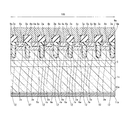
- the semiconductor device (reverse blocking IGBT) according to the first embodiment of the present invention includes an active region 100 and a breakdown voltage structure region 120 provided outside the active region 100 on a semiconductor substrate serving as the drift region 1. And a separation portion 130 provided outside the pressure-resistant structure region 120.
- the thickness of the semiconductor substrate may be, for example, 90 ⁇ m or more so as not to adversely affect the characteristics of the reverse blocking IGBT having a 600V breakdown voltage class.
- the semiconductor substrate for example, a semiconductor substrate made of single crystal silicon is used.
- the first main surface Y1 (front surface) and the second main surface Y2 (back surface) located on opposite sides of the drift region 1 are provided on the surface layer portion on the first main surface Y1 side.
- Two-conductivity (p-type) channel formation region 2 first conductivity-type (n + -type) first main electrode region 3, and second main surface Y2 of drift region 1 (surface layer portion on the back surface side of the semiconductor substrate)
- a vertical IGBT composed of the second main electrode region 10 of the second conductivity type (p-type) provided in the first is formed.
- Channel formation region 2 means a base region in an IGBT, but in a semiconductor device other than an IGBT, it means a region where a channel is formed on a surface equivalent to the base region of the IGBT.
- the “first main electrode region 3” and the “second main electrode region 10” mean the emitter region and the collector region of the IGBT as described at the beginning. A detailed description of the active region 100 will be described later.
- the breakdown voltage structure region 120 surrounds the active region 100 between the active region 100 and the isolation part 130.
- the breakdown voltage structure region 120 relaxes the electric field strength on the surface of the pn junction constituting the semiconductor device and realizes a desired breakdown voltage. A detailed description of the breakdown voltage structure region 120 will be described later.
- the separation unit 130 is provided at the outer peripheral end of the semiconductor substrate and surrounds the active region 100. In addition, the separation unit 130 separates, for example, crystal defects generated on the side surface of the semiconductor substrate and the active region 100 when dicing into individual chips.
- the isolation part 130 is provided with a second conductivity type (p-type) isolation region 31.
- the isolation region 31 is provided at the outer peripheral end of the drift region 1 and penetrates from the first main surface Y1 to the second main surface Y2 (from the front surface to the back surface) of the drift region 1.
- the isolation region 31 is in contact with the p-type second main electrode region 10 as a collector region provided on the back surface of the active region 100.
- the isolation region 31 when a reverse voltage is applied, the depletion layer is isolated from the second main electrode region (collector region) 10 provided on the back surface of the semiconductor substrate (the second main surface Y2 side of the drift region 1). It extends along the region 31. For this reason, it is possible to prevent the depletion layer from reaching the cut surface of the semiconductor substrate, thereby preventing the occurrence of leakage current.
- the semiconductor device (reverse blocking IGBT) according to the first embodiment of the present invention can obtain a reverse breakdown voltage.
- the semiconductor device (reverse blocking IGBT) according to the first embodiment of the present invention includes a first conductivity type (n-type) high concentration region (lifetime control region) 5 provided in the drift region 1.
- the active region 100 of the semiconductor device (reverse blocking IGBT) according to the first embodiment of the present invention shown in FIG. 1 will be described with reference to FIG.
- the active region 100 has a second conductivity type (p-type) channel as a base region on the surface of the semiconductor substrate to be the drift region 1 (on the first main surface Y1 side of the drift region 1).
- a formation region 2 is selectively provided.
- Channel formation region 2 has a higher impurity concentration than drift region 1.
- a first conductive type (n + type) first main electrode region 3 as an emitter region and a second conductive type (p + type) body region 4 are selectively provided on the channel forming region 2. ing.
- the body region 4 occupies a part of the region below the first main electrode region 3.
- the body region 4 has a higher impurity concentration than the channel formation region 2.
- the n-type high concentration region 5 is provided on the channel formation region 2 side in the drift region 1.
- the n-type high concentration region 5 is preferably provided so as to occupy a region below the channel formation region 2.
- the n-type high concentration region 5 is preferably provided so as to inhibit the depletion layer extending from the second main electrode region (collector region) 10 from approaching the p-type channel formation region 2. The reason is that the depletion layer extending from the second main electrode region (collector region) 10 toward the channel formation region 2 can be shortened to reduce the transport efficiency. This is because the leakage current when the reverse voltage is applied can be reduced.
- the n-type high concentration region 5 is irradiated with a predetermined amount of high energy protons from the first main surface Y1 side or the second main surface Y2 (the front surface side or the back surface side of the semiconductor substrate) of the drift region 1.
- the drift region 1 can be formed at an arbitrary depth and at an arbitrary concentration.
- a proton shield for example, aluminum or resist
- the n-type high concentration region 5 has a higher impurity concentration than the drift region 1.
- the n-type high concentration region 5 has an impurity concentration that is completely depleted when a depletion layer spreads from the channel formation region 2 toward the second main electrode region (collector region) 10.
- the total impurity amount of the n-type high concentration region 5 needs to be 2.0 ⁇ 10 12 cm ⁇ 2 or less at the maximum when the drift region 1 is silicon.
- the maximum total impurity amount of the n-type high concentration region 5 is expressed as follows from the one-dimensional Poisson equation.
- Equation (2) E: electric field strength
- Ecrit critical electric field strength
- q elementary charge
- N D donor concentration
- x distance extended by the depletion layer
- ⁇ Si relative dielectric constant of silicon
- ⁇ 0 dielectric constant of vacuum
- N D x Total impurity amount
- the n-type high-concentration region 5 may be contained in the n-type high-concentration region 5 so that the total impurity amount of the n-type impurities contained in the whole is 2.0 ⁇ 10 12 cm ⁇ 2 or less. It does not depend on the impurity concentration distribution.
- the first electrode as the first electrode is interposed through the gate insulating film 6 as the insulating film so as to straddle the drift region 1 from the first main electrode region 3.
- a gate electrode 7 is provided.
- the emitter electrode 9 as the second electrode is in contact with the first main electrode region 3.
- the emitter electrode 9 is electrically connected to the channel forming region 2 through the body region 4.
- the emitter electrode 9 is electrically insulated from the gate electrode 7 by the interlayer insulating film 8.
- the second main electrode region 10 is provided on the second main surface 2Y (the back surface of the semiconductor substrate) of the drift region 1 as described above.
- the collector electrode 11 as the third electrode is in contact with the second main electrode region 10.
- a deep p + -type extraction region (well region) 23 having the same potential as that of the emitter electrode 9 is formed at a terminal portion of the active region 100 with a predetermined width.
- the extraction region 23 is electrically connected to the emitter electrode 9 and is electrically connected to the first main electrode region 3 through the emitter electrode 9.
- the extraction region 23 is often formed at the same time as the channel formation region 2 and is an extraction region that functions to efficiently extract carriers in the breakdown voltage structure region 120 when a forward voltage is applied.
- the breakdown voltage structure region 120 includes a first conductivity surface Y1 (surface of the semiconductor substrate) of the drift region 1 and a second conductivity type (p-type) field limiting ring region (hereinafter referred to as FLR: Field Limiting) which is a floating region.
- FLR Field Limiting
- a plurality of rings 21 are provided.
- the FLR 21 is provided in a ring shape so as to surround the active region 100.
- the surface of the first main surface Y1 (front surface) of the drift region 1 where the FLR 21 is not provided is covered with an interlayer insulating film 8.
- FP Field Plate
- the FP 22 contacts the FLR 21.
- a field plate (hereinafter referred to as equipotential FP) 32 having the same potential as that of the isolation region 31 is provided on the interlayer insulating film 8 from the breakdown voltage structure region 120 to the isolation part 130.
- the equipotential FP 32 is in contact with and electrically connected to the separation region 31.
- the side close to the active region is referred to as a forward breakdown voltage structure region 121
- the side close to the isolation region 31 is referred to as a reverse breakdown voltage structure region 122 for convenience.
- the two breakdown voltage structure regions 121 and 122 are not overlapped for convenience, but can be overlapped with each other in an actual element.
- FIG. 4 is a characteristic diagram showing the electric field strength E in the active region 100 of the semiconductor device (reverse blocking IGBT) according to the first embodiment of the present invention.
- FIG. 4 shows the relationship between the height y from the bottom surface of the semiconductor substrate and the electric field E in the active region 100 of the semiconductor device (reverse blocking IGBT) according to the first embodiment of the present invention shown in FIG.
- the depletion layer can be stopped near the n-type high concentration region 5 at the time of reverse bias (dotted line in FIG. 4). It is.
- the n-type high concentration region 5 suppresses the extension width of the depletion layer to some extent, but a predetermined breakdown voltage can be maintained. This is because the n-type high concentration region 5 is provided under the above-described conditions.
- FIG. 5 is an impurity concentration profile diagram showing the distribution of impurity concentration along the cutting line YY in FIG.
- the impurity concentration in the semiconductor substrate was measured. From this impurity concentration, the total dose amount of the n-type high concentration region 5 was calculated.
- the total dose amount of the n-type high-concentration region 5 is a dose amount of the ion implantation when the n-type high-concentration region 5 is formed by a single ion implantation, and is obtained by a plurality of ion implantations. In the case where an n-type high concentration region is formed, it means the total dose amount of each ion implantation.
- the first measurement result 41 is the impurity concentration distribution in the drift region 1.
- the second measurement result 42 is a distribution of impurity concentrations in the channel formation region 2 and the body region 4.
- the third measurement result 43 is an impurity concentration distribution in the second main electrode region 10.
- the fourth measurement result 44 is an impurity concentration distribution of the n-type high concentration region 5. This shows that the n-type high concentration region 5 is formed at a position of about 10 ⁇ m from the surface.
- the impurity concentration at each depth of the fourth measurement result 44 was integrated to calculate the total dose amount of the n-type high concentration region 5.
- the distribution of the impurity concentration shown in FIG. 5 indicates what impurity concentration the conductivity type impurity exists in the depth direction in the semiconductor substrate.
- the impurity concentration is low in a region close to the substrate surface, the impurity concentration increases as the distance from the region decreases, and the impurity concentration decreases again. Therefore, by integrating the impurity concentration for each depth of the fourth measurement result 44, the total impurity amount of the n-type high concentration region 5 per unit area can be calculated.
- the total impurity amount of the entire n-type high concentration region 5 can be calculated.
- a value obtained by subtracting the total impurity amount of the high concentration region 5 portion of the drift region 1 from the total impurity amount of the n type high concentration region 5 thus calculated is the total dose amount of the n type high concentration region 5.
- the region 40 (shaded portion in FIG. 5) in the distribution shape of the impurity concentration distribution of the fourth measurement result 44 shown in FIG. 5 is the total dose amount of the n-type high concentration region 5.
- the total impurity amount of the high concentration region 5 portion of the drift region 1 is the total impurity amount of the drift region 1 in the region where the n-type high concentration region 5 is provided.
- the total impurity amount in the drift region 1 is calculated by the same method as that for the n-type high concentration region 5.
- FIG. 6 is a characteristic diagram showing the relationship between the total dose of the n-type high concentration region 5 and the forward breakdown voltage.
- the total dose amount of the n-type high concentration region 5 was variously changed, and a plurality of reverse blocking IGBTs of Examples were prepared.
- the total dose of the n-type high concentration region 5 is 1 ⁇ 10 11 to 1.2 ⁇ 10 12 cm ⁇ 2, and the position of the n-type high concentration region 5 is 10 ⁇ m from the channel formation region 2. did.
- Each forward breakdown voltage was measured with the gate-emitter short-circuited.
- a reverse blocking IGBT without the n-type high concentration region 5 was prepared (hereinafter referred to as a comparative example), and the forward breakdown voltage was measured.
- a comparative example a reverse blocking IGBT without the n-type high concentration region 5 was prepared (hereinafter referred to as a comparative example), and the forward breakdown voltage was measured.
- a comparative example a reverse blocking IGBT without
- the reverse blocking IGBT of the comparative example is shown as a total dose amount of zero. From the results shown in FIG. 6, it was found that the forward breakdown voltage is reduced by providing the n-type high concentration region 5. The reason is that a depletion layer extending in the drift region 1 from the channel formation region 2 toward the second main electrode region 10 by providing the n-type high concentration region 5 in a region near the channel formation region 2 of the drift region 1. Is shortened. It was found that when the total dose of the n-type high concentration region 5 is 4 ⁇ 10 11 cm ⁇ 2 or less, the rated voltage or more can be secured.
- FIG. 7 is a characteristic diagram showing the relationship between the total dose of the n-type high concentration region 5 and the reverse leakage current.
- the reverse blocking IGBT of the example used in FIG. 6 the reverse leakage current was measured.
- the reverse blocking IGBT of the comparative example is shown as a total dose amount of zero.
- the collector-emitter voltage was set to -600 V, and the measurement was performed with the gate-emitter short-circuited. From the results shown in FIG. 7, it was found that the reverse leakage current is reduced by providing the n-type high concentration region 5.
- the reverse leakage current sharply decreases until the total dose of the n-type high concentration region 5 is about 4.0 ⁇ 10 11 cm ⁇ 2, and the reverse leakage current exceeds 4.0 ⁇ 10 11 cm ⁇ 2 or more. It was found that the decrease in From the results of FIGS. 6 and 7, it can be said that the total dose amount of the n-type high concentration region 5 is preferably 4.0 ⁇ 10 11 cm ⁇ 2 or less and close to 4.0 ⁇ 10 11 cm ⁇ 2 .
- the breakdown voltage structure region 120 is from the outer peripheral end of the extraction region 23 having the same potential as the emitter electrode 9 to the inner peripheral end of the isolation region 31 having the same potential as the collector electrode 11, and the end of the n-type high concentration region 5.
- the position of the part is represented by a relative position with respect to the pressure-resistant structure region 120. That is, the end of the n-type high concentration region 5 when the outer peripheral end of the extraction region 23 having the same potential as the emitter electrode 9 is 0 and the inner peripheral end of the isolation region 31 having the same potential as the collector electrode 11 is 1.
- the position of the part was represented as L (FIG. 3).
- a negative value of the position L of the end portion of the n-type high concentration region 5 indicates that the n-type high concentration region 5 ends under the active region, and the end portion of the n-type high concentration region 5 ends.
- the position L of 1 is larger than 1 indicates that the n-type high concentration region 5 projects outward from the inner peripheral edge of the separation region 31.
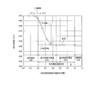
- FIG. 8 is a characteristic diagram showing the relationship between the end position L of the n-type high concentration region 5 and the forward breakdown voltage.
- FIG. 9 is opposite to the end position L of the n-type high concentration region 5. It is a characteristic view which shows the relationship with a direction leakage current.
- the total dose amount of the n-type high concentration region 5 is 2 ⁇ 10 11 cm ⁇ 2 .
- the withstand voltage structure region 120 includes the forward withstand voltage structure region 121 and the reverse withstand voltage structure region 122, and is optimum so as to obtain predetermined forward withstand voltage, reverse withstand voltage, and charge resistance, respectively. Designed to become. From FIG.
- the forward breakdown voltage shows the highest value when the position L of the end portion of the n-type high concentration region 5 is in the active region or slightly on the active region side from the end portion of the active region.
- the position where the forward breakdown voltage starts to decrease is the position where the n-type high concentration region 5 starts to be applied to the extraction region 23. Further, it was found that even if the n-type high concentration region 5 is provided up to the end of the active region, the amount of decrease in the forward breakdown voltage is about 1%. Further, when the n-type high concentration region 5 is projected from the forward breakdown voltage structure region 121 side to 36% or more of the width W of the breakdown voltage structure region 120, the forward breakdown voltage is reduced to about 12%. However, it turned out that it took a stable value.
- the reverse leakage current decreases even when the position L of the end portion of the n-type high concentration region 5 is inside the end portion of the active region 100.
- the amount of decrease in reverse leakage current begins to moderate.
- the width W is in the range of + 10% to ⁇ 10%, it is possible to reduce the reverse leakage current while suppressing the decrease in the forward breakdown voltage.
- the width W of the pressure-resistant structure region 120 is in the range of + 5% to ⁇ 5%.
- the position L of the end portion of the n-type high concentration region 5 to be 36% or more of the width W of the breakdown voltage structure region 120, even when the width of the n-type high concentration region 5 varies, it can be stably performed. The forward breakdown voltage and reverse leakage current can be maintained.
- the first main electrode region (emitter region) 3, the second main electrode region (collector region) 10 By providing an n-type high concentration region 5 having a predetermined concentration in a region close to the channel formation region (base region) 2 of the drift region 1 between the two regions, reverse leakage is maintained while maintaining a predetermined forward breakdown voltage. The current can be reduced.
- the forward breakdown voltage is 600 V and the reverse leakage current can be reduced by about 60% compared to the case where the n-type high concentration region 5 is not provided.
- a neutral region remains between the n-type high concentration region 5 and the channel formation region 2.
- Residual carriers provide soft recovery and suppress voltage and current waveform vibration during reverse recovery. It was also found that by providing the n-type high concentration region 5 up to the end of the active region 100, it is possible to reduce the reverse leakage current while suppressing the amount of decrease in the forward breakdown voltage. Further, by providing the n-type high concentration region 5 up to 36% or more of the width W of the breakdown voltage structure region 120, even if the width of the n-type high concentration region 5 varies, the forward breakdown voltage and the reverse direction can be stabilized. It was found that leakage current can be obtained.
- the drift region 1 has a resistivity at which a depletion layer extending from the second main electrode region 10 toward the extraction region 23 (extraction region) does not reach this extraction region when a reverse voltage equal to the rated voltage is applied.
- the planar gate type reverse blocking IGBT is used as a model.
- it is good also as a structure which reversed all the n-type and p-type.
- the n-type high concentration region 5 can be formed by, for example, selective proton irradiation and donor formation by heat treatment.
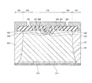
- FIG. 10 is a cross-sectional view corresponding to FIG. 2, and is a cross-sectional view showing a configuration of the active region when the active region 100 of the planar gate type reverse blocking IGBT of FIG. 1 is a trench gate type IGBT.
- the semiconductor device according to the second embodiment of the present invention is a trench gate type reverse blocking IGBT mainly composed of a semiconductor substrate which becomes a drift region 1a of the first conductivity type (n ⁇ type). is there.
- the semiconductor device (reverse blocking IGBT) according to the second embodiment of the present invention is not shown in detail, but becomes the drift region 1a as in the semiconductor device according to the first embodiment of the present invention.
- An active region 100 shown in FIG. 1, a breakdown voltage structure region 120 provided outside the active region 100, and a separation unit 130 provided outside the breakdown voltage structure region 120 are provided on a semiconductor substrate.
- the structure of the breakdown voltage structure region is the same as that of the above-described planar gate type reverse blocking IGBT.
- a plurality of trench grooves 12 are formed at a predetermined interval on the front surface (first main surface Y1 of the drift region 1a) of the semiconductor substrate to be the first conductivity type (n ⁇ type) drift region 1a. Is provided.
- a second conductivity type (p-type) channel formation region 2 a is provided so as to be sandwiched between the trench grooves 12.
- the p-type channel formation region 2a has a higher impurity concentration than the n ⁇ -type drift region 1a.
- the first main electrode region 3 a of the first conductivity type (n + type) and the second main electrode region 3 a are formed on the surface layer on the substrate front surface side of the p-type channel formation region 2 a.
- Conductive type (p + type) body region 4a is selectively provided.
- the p + type body region 4a has a higher impurity concentration than the p type channel formation region 2a.
- a portion having a configuration in which an n + -type first main electrode region 3a and a p + -type body region 4a are provided From the configuration, portions having a configuration without the n + -type first main electrode region 3a are alternately arranged.
- the n-type high concentration region 5 is provided in a region close to the surface between the n ⁇ -type drift region 1a and the p-type channel formation region 2a.
- the emitter electrode 9a as the second electrode is in common contact with the surfaces of the n + -type first main electrode region 3a and the p + -type body region 4a.
- the emitter electrode 9a is electrically insulated from the gate electrode 7a as the first electrode by the interlayer insulating film 8a.
- the second main surface 2Y of the drift region 1 is provided with a second main electrode region 10a as a collector region.
- a collector electrode 11a as a third electrode provided on the second main surface 2Y side (the back surface of the semiconductor substrate) of the drift region 1 is in contact with the second main electrode region 10a.
- the structure of the trench groove 12 will be further described.
- the trench groove 12 must have a depth that penetrates the n + -type first main electrode region 3a and the p-type channel formation region 2a, but for the n-type high concentration region 5 described above,
- the intermediate depth of the n-type high concentration region 5 may be a depth that penetrates or a depth that does not reach.
- the MOS gate structure (trench gate MOS structure) formed in the trench groove 12 is provided with a gate insulating film 6a as an insulating film along the inner wall of the trench groove 12 in the same manner as in the prior art.
- a gate electrode 7a as a first electrode made of polysilicon is buried via a gate insulating film 6a.
- the n + type first main electrode region 3a and the p + type are provided between the adjacent trench grooves 12 as the surface structure.
- the portion of the structure provided with the body region 4a and the portion of the structure without the n + -type first main electrode region 3a are alternately arranged. If formed, the effect of forming the n-type high-concentration region 5 can be obtained even if the trench gate type IGBT has another configuration.
- the semiconductor device according to the present invention is useful for a semiconductor element that requires a withstand voltage characteristic with respect to forward and reverse voltages, such as a switch used in a series conversion circuit such as a matrix converter.
Landscapes
- Metal-Oxide And Bipolar Metal-Oxide Semiconductor Integrated Circuits (AREA)
- Electrodes Of Semiconductors (AREA)
- Insulated Gate Type Field-Effect Transistor (AREA)
Abstract
半導体装置は、第1導電型のドリフト領域(1)と、ドリフト領域の第1主面に選択的に設けられた第2導電型のチャネル形成領域(2)と、チャネル形成領域の上部に選択的に設けられた第1導電型の第1主電極領域(3)と、ドリフト領域の第2主面に設けられた第2導電型の第2主電極領域(10)と、チャネル形成領域の下のドリフト領域にチャネル形成領域から離れて設けられた第1導電型の高濃度領域(5)とを備えている。そして、高濃度領域は、ドリフト領域よりも高い不純物濃度であり、かつ、高濃度領域中の第1導電型不純物の総不純物量が2.0×1012cm-2以下となる不純物濃度を有する。
Description
この発明は、半導体装置に関し、特に、逆阻止型絶縁ゲートバイポーラトランジスタを有する半導体装置に適用して有効な技術に関する。
近年、半導体素子を用いた、AC(交流)/AC変換やAC/DC(直流)変換,DC/AC変換などの電力変換装置において、電界コンデンサや直流リアクトルなどで構成される直流平滑回路が不要な直接変換回路として、例えばマトリクスコンバータが公知である。
マトリクスコンバータは、複数の交流スイッチから構成されている。交流スイッチには、交流電圧が印加されるため、順方向および逆方向の双方の耐圧(以下、順方向耐圧および逆方向耐圧とする)を有する構成が要求され、回路の小型化、軽量化、高効率化、高速応答化および低コスト化等の観点から、双方向スイッチング素子が着目されている。
このような双方向スイッチング素子として、例えば、逆阻止型絶縁ゲートバイポーラトランジスタ(以下、逆阻止IGBT:Insulated Gate Bipolar Transisterとする)を2つ逆並列に接続して構成されたスイッチが公知である。
マトリクスコンバータは、複数の交流スイッチから構成されている。交流スイッチには、交流電圧が印加されるため、順方向および逆方向の双方の耐圧(以下、順方向耐圧および逆方向耐圧とする)を有する構成が要求され、回路の小型化、軽量化、高効率化、高速応答化および低コスト化等の観点から、双方向スイッチング素子が着目されている。
このような双方向スイッチング素子として、例えば、逆阻止型絶縁ゲートバイポーラトランジスタ(以下、逆阻止IGBT:Insulated Gate Bipolar Transisterとする)を2つ逆並列に接続して構成されたスイッチが公知である。
逆阻止IGBTを逆並列接続したスイッチ素子として用いる場合には、逆阻止IGBTは、IGBTとダイオードの働きを合わせ持つ。逆阻止IGBTをダイオードとして働かせる場合はIGBTのゲートにオン信号を与え、チャネルを常に開いた状態にしておく。これによって、逆阻止IGBTのpコレクタ領域-nドリフト領域-nチャネル領域-nエミッタ領域により、pnダイオードが構成される。
逆阻止IGBTのゲートにオン信号を印加して、ダイオードモードにして、このダイオードに順電流を流す。この順電流によりダイオードのドリフト領域には過剰キャリアが蓄積される。その後で、ダイオードに逆電圧を印加すると、蓄積した過剰キャリアが掃き出されて、逆回復電流が流れて逆回復電圧が発生する。過剰キャリアが素早く掃き出され残留キャリアが少ないと逆回復電圧・電流は振動する。この振動が大きくなると、逆回復破壊が起こるので、この振動を小さく抑制することが望まれる。
逆阻止IGBTのゲートにオン信号を印加して、ダイオードモードにして、このダイオードに順電流を流す。この順電流によりダイオードのドリフト領域には過剰キャリアが蓄積される。その後で、ダイオードに逆電圧を印加すると、蓄積した過剰キャリアが掃き出されて、逆回復電流が流れて逆回復電圧が発生する。過剰キャリアが素早く掃き出され残留キャリアが少ないと逆回復電圧・電流は振動する。この振動が大きくなると、逆回復破壊が起こるので、この振動を小さく抑制することが望まれる。
図11は、従来の逆阻止IGBTを示す断面図である。図11に示すように、逆阻止IGBTは、n-型の半導体基板の外周端部に、活性領域310を囲む分離部330が設けられている。活性領域310には、n-型のドリフト領域201、p型のベース領域202、n+型のエミッタ領域203およびp型のコレクタ領域210からなる縦型のIGBTが構成されている。分離部330には、例えば半導体基板のおもて面から裏面まで貫通するp型の分離領域231が設けられている。分離領域231は、活性領域310の裏面に設けられたコレクタ領域210に接する。分離部330と活性領域310との間には、耐圧構造領域320が設けられている。耐圧構造領域320は、半導体装置を構成するpn接合表面の電界強度を緩和し、所望の耐圧を実現する。
図12は、図11に示す逆阻止IGBTの活性領域310について詳細に示す断面図である。活性領域310には、n-型の半導体基板からなるドリフト領域201の表面に、p型のベース領域202が選択的に設けられている。ベース領域202は、ドリフト領域201よりも高い不純物濃度を有する。ベース領域202の表面には、n+型のエミッタ領域203およびp+型のボディ領域204が選択的に設けられている。ゲート電極207は、ゲート絶縁膜206を介して、エミッタ領域203およびベース領域202の一部を覆う。エミッタ電極209は、エミッタ領域203およびボディ領域204に接する。また、エミッタ電極209は、層間絶縁膜208によってゲート電極207と電気的に絶縁されている。ドリフト領域201の第2主面Y2(裏面)には、p型のコレクタ領域210およびコレクタ電極211が設けられている。
このような逆阻止IGBTは、浮遊帯域溶融(FZ:Floating Zone)法によって作製されたシリコン(Si)基板を用いることで、オフ時にエミッタ側から拡がる空乏層がコレクタ側に到達しないノンパンチスルー(NPT:Non Punch Through)型とすることができる。FZ法によって作製されたシリコン基板を研削する技術が向上したことにより、シリコン基板の厚さを、例えばIGBTの定格電圧を600Vとした場合に100μm程度、1200Vとした場合に180μm程度まで薄くすることができるからである。NPT型IGBTは、コレクタ領域の厚さを薄く、かつコレクタ領域の不純物濃度を低く形成することで、コレクタ領域からの少数キャリアの注入効率を下げ、輸送効率を上げる構成となっている。このように、NPT型の逆阻止IGBTとすることで、オン電圧特性とターンオフ損失とのトレードオフ関係による問題を改善し、オン電圧の低減およびターンオフ損失の低減をともに実現している。
このような逆阻止IGBTとして、半導体基板の表面にpベース領域を形成し、このpベース領域の表面にn+エミッタ領域を形成し、この半導体基板の外周部と裏面側に、pベース領域を取り囲むようにp+コレクタ領域(側面に形成されるp+領域と裏面側p+コレクタ領域)が形成され、裏面のp+コレクタ領域の厚さを1μm程度とした装置が提案されている(例えば、下記特許文献1参照)。
また、別の装置として、次のような装置が提案されている。半導体基板が該半導体基板を一層とする層の両側に形成される順逆耐圧用pn接合を少なくとも備え、これらの両pn接合の耐圧接合終端構造が分離拡散領域により前記半導体基板の第一主面側に備える高耐圧半導体装置において、前記半導体基板を一層とする層が第一主面から内部に向かって実質的に一定の不純物濃度分布または不純物濃度が内部に向かって減少する領域を有している(例えば、下記特許文献2参照)。
また、別の装置として、次のような装置が提案されている。半導体基板が該半導体基板を一層とする層の両側に形成される順逆耐圧用pn接合を少なくとも備え、これらの両pn接合の耐圧接合終端構造が分離拡散領域により前記半導体基板の第一主面側に備える高耐圧半導体装置において、前記半導体基板を一層とする層が第一主面から内部に向かって実質的に一定の不純物濃度分布または不純物濃度が内部に向かって減少する領域を有している(例えば、下記特許文献2参照)。
図13は、従来の逆阻止IGBTの別の一例を示す断面図である。図13に示す逆阻止IGBTでは、ドリフト領域201とベース領域202の間に、n型のシェル領域301が設けられている。シェル領域301は、ドリフト領域201よりも高い不純物濃度を有する。ドリフト領域201とコレクタ領域210の間には、n型のバッファ領域302が設けられている。バッファ領域302は、ドリフト領域201よりも高い不純物濃度を有する。それ以外の構成は、図11に示す逆阻止IGBTと同様である。このように、ドリフト領域201とベース領域202との界面、またはドリフト領域201とコレクタ領域210との界面、もしくはその両方の界面に、ドリフト領域201と同一導電型で、ドリフト領域201より高い不純物濃度の領域(シェル領域301,バッファ領域302)を設けることで、特性向上を図ったIGBTが公知である。
このようなIGBTとして、次のような装置が提案されている。導電型が交互に異なる互いに重なり合う領域からなるIGBTは、パンチスルーに対して寸法決定されており、2つの緩衝層を備えている。緩衝層は、ドリフト領域と同じ導電型で高不純物濃度にドープされている。それによって、構造素子は、対照的に遮断されるようになっている。また、順方向耐圧および逆方向耐圧がほぼ同様の値となるIGBTとすることができる(例えば、下記特許文献3参照)。
また別の装置として、次のような装置が提案されている。上記緩衝層を有するIGBTであって、順方向・逆方向ともにパンチスルーしないように寸法決定されており、緩衝層は、ドリフト領域と同じ導電型で高不純物濃度にドープされている(例えば、下記特許文献4参照)。
また別の装置として、次のような装置が提案されている。上記緩衝層を有するIGBTであって、順方向・逆方向ともにパンチスルーしないように寸法決定されており、緩衝層は、ドリフト領域と同じ導電型で高不純物濃度にドープされている(例えば、下記特許文献4参照)。
また別の装置として、次のような装置が提案されている。pベース領域とnドリフト領域との境界の少なくとも一部にnドリフト領域と同じ導電型で、より高不純物濃度の高濃度領域を設けている。これにより、チャネル長を短縮し、オン状態の電圧降下を低減する(例えば、下記特許文献5参照)。
また、別の装置として、次のような装置が提案されている。nドリフト領域のpベース領域近傍にnドリフト領域と同じ導電型で、より高不純物濃度の高濃度領域を設けている。これにより、オン状態の電圧降下を低減する(例えば、下記特許文献6参照)。
また、別の装置として、次のような装置が提案されている。nドリフト領域のpベース領域近傍にnドリフト領域と同じ導電型で、より高不純物濃度の高濃度領域を設けている。これにより、オン状態の電圧降下を低減する(例えば、下記特許文献6参照)。
また、別の装置として、次のような装置が提案されている。nベース層のpコレクタ領域に近い部分に短寿命領域を形成する。短寿命領域は、n型でnベース層よりも高濃度にドープされている。これにより、NPT型IGBTの漏れ電流を低減する(例えば、下記特許文献7参照)。
また、別の装置として、次のような装置が提案されている。nベース層のpコレクタ領域に近い部分にnドリフト領域と同じ導電型で、より高不純物濃度の高濃度領域を設けている。これにより、コレクタ領域に部分的な欠損があっても、オン状態の電圧降下特性の上昇や耐圧特性の低下に影響が出にくくする(例えば、下記特許文献8参照)。
また、別の装置として、NPT型IGBTにおいて、pベース領域側のn-ドリフト領域にn+領域を設けることでオン電圧とオフ電圧(順方向電圧)の双方を改善できることが記載されている(例えば、下記特許文献9参照)。
また、別の装置として、次のような装置が提案されている。nベース層のpコレクタ領域に近い部分にnドリフト領域と同じ導電型で、より高不純物濃度の高濃度領域を設けている。これにより、コレクタ領域に部分的な欠損があっても、オン状態の電圧降下特性の上昇や耐圧特性の低下に影響が出にくくする(例えば、下記特許文献8参照)。
また、別の装置として、NPT型IGBTにおいて、pベース領域側のn-ドリフト領域にn+領域を設けることでオン電圧とオフ電圧(順方向電圧)の双方を改善できることが記載されている(例えば、下記特許文献9参照)。
しかしながら、上述した特許文献4に示す技術では、IGBTのラッチアップ耐量向上の目的でpベース層ないに形成される高濃度p型ボディ領域の影響で、順方向漏れ電流に対して、逆方向漏れ電流が大きくなるという問題点がある。
また、上述した特許文献3に示す技術では、次に示すような問題が生じる。図13に示した基板底面からの高さyと電界強度Eとの関係を示す特性図を用いて説明する。図13に示す逆阻止IGBTでは、シェル領域301およびバッファ領域302が設けられていることで、半導体基板内の電界が急激に高くなってしまう。例えば、順バイアス時(図13の実線)、ベース領域202とシェル領域301の界面近傍の領域で、電界が急激に高くなってしまう。一方、逆バイアス時(図13の点線)、コレクタ領域210とバッファ領域302の界面近傍の領域で、電界が急激に高くなってしまう。このため、順方向耐圧および逆方向耐圧が低減してしまうことが多い。すなわち、シェル領域301およびバッファ領域302により、実際に得ることができるはずの順方向耐圧および逆方向耐圧を実現することができない恐れが生じる。
また、上述した特許文献3に示す技術では、次に示すような問題が生じる。図13に示した基板底面からの高さyと電界強度Eとの関係を示す特性図を用いて説明する。図13に示す逆阻止IGBTでは、シェル領域301およびバッファ領域302が設けられていることで、半導体基板内の電界が急激に高くなってしまう。例えば、順バイアス時(図13の実線)、ベース領域202とシェル領域301の界面近傍の領域で、電界が急激に高くなってしまう。一方、逆バイアス時(図13の点線)、コレクタ領域210とバッファ領域302の界面近傍の領域で、電界が急激に高くなってしまう。このため、順方向耐圧および逆方向耐圧が低減してしまうことが多い。すなわち、シェル領域301およびバッファ領域302により、実際に得ることができるはずの順方向耐圧および逆方向耐圧を実現することができない恐れが生じる。
このような問題は、ドリフト領域の不純物濃度を低くすることで回避することができることが知られている。しかしながら、ドリフト領域の不純物濃度を低くすることで、半導体装置の動作中に空乏層がバッファ領域302に達し、リーチスルー現象が発生してしまう。このため、ターンオフ時の電圧波形および電流波形(以下、ターンオフ波形とする)が振動してしまうという問題が生じる。また、逆阻止IGBTは、オン状態から逆阻止状態に切り換わるとき、過渡的に大きな電流が流れる特性(逆回復特性)を有する。このため、逆回復時の電圧波形および電流波形(以下、逆回復波形とする)が振動しやすいという問題が生じる。ターンオフ波形および逆回復波形が振動した場合、ノイズが発生してしまったり、電圧波形の振動が非常に大きくなったときに半導体装置が破壊されたりする恐れが生じる。
また、上述した特許文献3に示す技術では、n型シェル領域201に重なるようにp型ベース領域を形成するために、n型シェル領域201の濃度および深さ制御が困難であるという問題点を有する。また、一般的にターンオフ耐量向上の目的で活性領域端部に形成される、エミッタ電極に接続された深いp型領域の部分に関する記述がなく、深いp型領域を覆うようにn型シェル領域201を形成するためには形成プロセスの煩雑化を生じることが懸念され、深いp型領域を覆うようにn型シェル領域201を形成しない場合には、逆漏れ電流の低減が限定的であることが懸念される。
同様の懸念点は、上述した特許文献6に示す技術を逆阻止IGBTに用いても考慮可能である。
また、上述の特許文献9に示す技術では、逆阻止IGBTについての記載はない。したがって、逆電圧が印加されたときのn+領域の作用および逆漏れ電流については記載されていない。
同様の懸念点は、上述した特許文献6に示す技術を逆阻止IGBTに用いても考慮可能である。
また、上述の特許文献9に示す技術では、逆阻止IGBTについての記載はない。したがって、逆電圧が印加されたときのn+領域の作用および逆漏れ電流については記載されていない。
この発明は、上述した従来技術による問題点を解消するため、逆方向漏れ電流を低減することを目的とする。
上述した課題を解決し、本発明の目的を達成するため、本発明の一態様に係る半導体装置は、互いに反対側に位置する第1主面及び第2主面を有する第1導電型のドリフト領域と、ドリフト領域の第1主面に選択的に設けられた第2導電型のチャネル形成領域と、チャネル形成領域の上部に選択的に設けられた第1導電型の第1主電極領域と、ドリフト領域の第2主面に設けられた第2導電型の第2主電極領域と、チャネル形成領域の下のドリフト領域にチャネル形成領域から離れて設けられた第1導電型の高濃度領域と、ドリフト領域の外周であってチャネル形成領域を取り囲むように設けられ、第1主電極領域に接続された第2導電型の引き抜き領域と、引き抜き領域の外周であって引き抜き領域を取り囲むように設けられ、順方向耐圧構造と逆方向耐圧構造とを含む耐圧構造領域と、耐圧構造領域の外周であって、ドリフト領域の外周端部に設けられ、ドリフト領域の第1主面から第2主面まで貫通し、第2主電極領域に接する第2導電型の分離領域と、を備え、高濃度領域は、ドリフト領域よりも高い不純物濃度であり、かつ、高濃度領域中の第1導電型不純物の総不純物量が2.0×1012cm-2以下となる不純物濃度を有することを特徴としている。
本発明に係る半導体装置によれば、逆方向漏れ電流を低減することができるという効果を奏する。
以下、本発明の第1および第2の実施形態に係る半導体装置について、図面を参照して詳細に説明する。
本明細書において、「主電極領域」とは、IGBTにおいてエミッタ領域又はコレクタ領域の何れか一方となる低比抵抗の半導体領域を意味する。電界効果トランジスタ(FET)においては、ソース領域又はドレイン領域の何れか一方となる半導体領域を意味するので「半導体装置」に依拠した名称となる。より具体的には、上記の「一方となる半導体領域」を「第1主電極領域」として定義すれば、「他方の半導体領域」は、「第2主電極領域」となる。すなわち、「第2主電極領域」とはIGBTにおいては第1主電極領域とはならないエミッタ領域又はコレクタ領域の何れか一方となる半導体領域、FETにおいては上記第1主電極領域とはならないソース領域又はドレイン領域の何れか一方となる半導体領域を意味する。以下の第1及び第2の実施形態では、逆阻止IGBTに着目して説明するので、エミッタ領域を「第1主電極領域」、コレクタ領域を「第2主電極領域」と呼ぶ。
本明細書において、「主電極領域」とは、IGBTにおいてエミッタ領域又はコレクタ領域の何れか一方となる低比抵抗の半導体領域を意味する。電界効果トランジスタ(FET)においては、ソース領域又はドレイン領域の何れか一方となる半導体領域を意味するので「半導体装置」に依拠した名称となる。より具体的には、上記の「一方となる半導体領域」を「第1主電極領域」として定義すれば、「他方の半導体領域」は、「第2主電極領域」となる。すなわち、「第2主電極領域」とはIGBTにおいては第1主電極領域とはならないエミッタ領域又はコレクタ領域の何れか一方となる半導体領域、FETにおいては上記第1主電極領域とはならないソース領域又はドレイン領域の何れか一方となる半導体領域を意味する。以下の第1及び第2の実施形態では、逆阻止IGBTに着目して説明するので、エミッタ領域を「第1主電極領域」、コレクタ領域を「第2主電極領域」と呼ぶ。
以下の第1および第2の実施形態の説明では、第1導電型がn型、第2導電型がp型の場合について例示的に説明するが、導電型を逆の関係に選択して、第1導電型をp型、第2導電型をn型としても構わない。
また、本明細書および添付図面においては、n又はpを冠記した層や領域では、それぞれ電子又は正孔が多数キャリアであることを意味する。また、nやpに付す+および-は、+および-の付記されていない半導体領域に比してそれぞれ相対的に不純物濃度が高い又は低い半導体領域であることを意味する。
また、本明細書および添付図面においては、n又はpを冠記した層や領域では、それぞれ電子又は正孔が多数キャリアであることを意味する。また、nやpに付す+および-は、+および-の付記されていない半導体領域に比してそれぞれ相対的に不純物濃度が高い又は低い半導体領域であることを意味する。
なお、以下の第1および第2の実施形態の説明および添付図面において、同様の構成には同一の符号を付し、重複する説明を省略する。
また、第1および第2の実施形態で説明される添付図面は、見易く又は理解し易くするために正確なスケール、寸法で描かれていない。本発明はその要旨を超えない限り、以下に説明する第1および第2の実施形態の記載に限定されるものではなない。
以下の第1の実施形態では、本発明の「半導体装置」としてプレーナゲート型の逆阻止IGBTに着目して例示的に説明し、以下の第2の実施形態では、本発明の「半導体装置」としてトレンチゲート型逆阻止IGBTに着目して例示的に説明する。
また、第1および第2の実施形態で説明される添付図面は、見易く又は理解し易くするために正確なスケール、寸法で描かれていない。本発明はその要旨を超えない限り、以下に説明する第1および第2の実施形態の記載に限定されるものではなない。
以下の第1の実施形態では、本発明の「半導体装置」としてプレーナゲート型の逆阻止IGBTに着目して例示的に説明し、以下の第2の実施形態では、本発明の「半導体装置」としてトレンチゲート型逆阻止IGBTに着目して例示的に説明する。
(第1の実施形態)
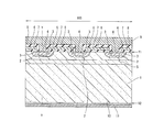
図1に示すように、本発明の第1の実施形態に係る半導体装置は、第1導電型(n-型)のドリフト領域1となる半導体基板を主体にしたプレーナゲート型の逆阻止IGBTである。また、本発明の第1の実施形態に係る半導体装置(逆阻止IGBT)は、ドリフト領域1となる半導体基板上に、活性領域100と、活性領域100の外側に設けられた耐圧構造領域120と、耐圧構造領域120の外側に設けられた分離部130とを備えている。半導体基板の厚さは、例えば600V耐圧クラスの逆阻止IGBTの特性に悪影響を及ぼさないためには、例えば90μm以上であればよい。半導体基板としては、例えば単結晶シリコンからなる半導体基板が用いられている。
図1に示すように、本発明の第1の実施形態に係る半導体装置は、第1導電型(n-型)のドリフト領域1となる半導体基板を主体にしたプレーナゲート型の逆阻止IGBTである。また、本発明の第1の実施形態に係る半導体装置(逆阻止IGBT)は、ドリフト領域1となる半導体基板上に、活性領域100と、活性領域100の外側に設けられた耐圧構造領域120と、耐圧構造領域120の外側に設けられた分離部130とを備えている。半導体基板の厚さは、例えば600V耐圧クラスの逆阻止IGBTの特性に悪影響を及ぼさないためには、例えば90μm以上であればよい。半導体基板としては、例えば単結晶シリコンからなる半導体基板が用いられている。
活性領域100には、ドリフト領域1の互いに反対側に位置する第1主面Y1(表面)及び第2主面Y2(裏面)のうちの第1主面Y1側の表層部に設けられた第2導電型(p型)のチャネル形成領域2、第1導電型(n+型)の第1主電極領域3、およびドリフト領域1の第2主面Y2(半導体基板の裏面側の表層部)に設けられた第2導電型(p型)の第2主電極領域10からなる縦型のIGBTが構成されている。「チャネル形成領域2」は、IGBTにおいてはベース領域を意味するが、IGBT以外の半導体装置においてはIGBTのベース領域に等価な表面にチャネルが形成される領域を意味する。また、「第1主電極領域3」、「第2主電極領域10」は、冒頭で述べたとおりIGBTのそれぞれエミッタ領域、コレクタ領域を意味する。活性領域100の詳細な説明については後述する。
耐圧構造領域120は、活性領域100と分離部130との間で、活性領域100を囲む。耐圧構造領域120は、半導体装置を構成するpn接合表面の電界強度を緩和し所望の耐圧を実現している。耐圧構造領域120の詳細な説明については後述する。
分離部130は、半導体基板の外周端部に設けられ、活性領域100を囲む。また、分離部130は、例えば個々のチップにダイシングされる際に半導体基板の側面に生じた結晶欠陥と活性領域100とを分離する。分離部130には、第2導電型(p型)の分離領域31が設けられている。分離領域31は、ドリフト領域1の外周端部に設けられ、ドリフト領域1の第1主面Y1から第2主面Y2(表面から裏面)まで貫通する。また、分離領域31は、活性領域100の裏面に設けられたコレクタ領域としてのp型の第2主電極領域10に接する。分離領域31を設けることで、逆方向電圧の印加時、空乏層が半導体基板の裏面(ドリフト領域1の第2主面Y2側)に設けられた第2主電極領域(コレクタ領域)10から分離領域31に沿って伸びる。このため、空乏層が半導体基板の切断面に到達することを防ぐことができ、漏れ電流の発生を防止する。これにより、本発明の第1の実施形態に係る半導体装置(逆阻止IGBT)は逆方向耐圧を得ることができる。
分離部130は、半導体基板の外周端部に設けられ、活性領域100を囲む。また、分離部130は、例えば個々のチップにダイシングされる際に半導体基板の側面に生じた結晶欠陥と活性領域100とを分離する。分離部130には、第2導電型(p型)の分離領域31が設けられている。分離領域31は、ドリフト領域1の外周端部に設けられ、ドリフト領域1の第1主面Y1から第2主面Y2(表面から裏面)まで貫通する。また、分離領域31は、活性領域100の裏面に設けられたコレクタ領域としてのp型の第2主電極領域10に接する。分離領域31を設けることで、逆方向電圧の印加時、空乏層が半導体基板の裏面(ドリフト領域1の第2主面Y2側)に設けられた第2主電極領域(コレクタ領域)10から分離領域31に沿って伸びる。このため、空乏層が半導体基板の切断面に到達することを防ぐことができ、漏れ電流の発生を防止する。これにより、本発明の第1の実施形態に係る半導体装置(逆阻止IGBT)は逆方向耐圧を得ることができる。
本発明の第1の実施形態に係る半導体装置(逆阻止IGBT)は、ドリフト領域1に設けられた第1導電型(n型)の高濃度領域(ライフタイム制御領域)5を備えている。
次に、図1に示す本発明の第1の実施形態に係る半導体装置(逆阻止IGBT)の活性領域100について、図2を用いて説明する。
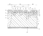
図2に示すように、活性領域100には、ドリフト領域1となる半導体基板の表面(ドリフト領域1の第1主面Y1側)に、ベース領域としての第2導電型(p型)のチャネル形成領域2が選択的に設けられている。チャネル形成領域2は、ドリフト領域1よりも高い不純物濃度を有する。チャネル形成領域2の上部には、エミッタ領域としての第1導電型(n+型)の第1主電極領域3、および第2導電型(p+型)のボディ領域4が選択的に設けられている。ボディ領域4は、第1主電極領域3の下の領域の一部を占める。また、ボディ領域4は、チャネル形成領域2よりも高い不純物濃度を有する。
次に、図1に示す本発明の第1の実施形態に係る半導体装置(逆阻止IGBT)の活性領域100について、図2を用いて説明する。
図2に示すように、活性領域100には、ドリフト領域1となる半導体基板の表面(ドリフト領域1の第1主面Y1側)に、ベース領域としての第2導電型(p型)のチャネル形成領域2が選択的に設けられている。チャネル形成領域2は、ドリフト領域1よりも高い不純物濃度を有する。チャネル形成領域2の上部には、エミッタ領域としての第1導電型(n+型)の第1主電極領域3、および第2導電型(p+型)のボディ領域4が選択的に設けられている。ボディ領域4は、第1主電極領域3の下の領域の一部を占める。また、ボディ領域4は、チャネル形成領域2よりも高い不純物濃度を有する。
n型の高濃度領域5は、ドリフト領域1中のチャネル形成領域2側に設けられている。また、n型の高濃度領域5は、チャネル形成領域2の下の領域を占めるように設けられるのがよい。つまり、n型の高濃度領域5は、第2主電極領域(コレクタ領域)10から広がる空乏層がp型のチャネル形成領域2に近づくのを阻害するように設けられるのがよい。その理由は、第2主電極領域(コレクタ領域)10からチャネル形成領域2へ向かって広がる空乏層の伸びを短くし、輸送効率を低減することができるからである。これによって、逆方向電圧印加時の漏れ電流を低減することができるからである。このようなn型の高濃度領域5は、ドリフト領域1の第1主面Y1側もしくは第2主面Y2(半導体基板の表面側もしくは裏面側)から所定の量の高エネルギのプロトンを照射し、所定の熱処理を行うことでドリフト領域1の任意の深さに任意の濃度で形成することが可能である。また、ドリフト領域1の一部にのみn型の高濃度領域5を形成する場合には、プロトン遮蔽物(たとえば、アルミニウムやレジスト等)を所定の場所におくことで可能である。
また、n型の高濃度領域5は、ドリフト領域1よりも高い不純物濃度を有する。そして、n型の高濃度領域5は、チャネル形成領域2から第2主電極領域(コレクタ領域)10に向かって空乏層が広がった場合に、完全に空乏化する不純物濃度を有する。n型の高濃度領域5の総不純物量は、ドリフト領域1がシリコンの場合、最高でも2.0×1012cm-2以下にする必要がある。n型の高濃度領域5の最大の総不純物量は1次元のポアソン方程式から、下記のように表される。


ここで、E:電界強度、Ecrit:臨界電界強度、q:素電荷、ND:ドナー濃度、x:空乏層の伸びる距離、εSi:シリコンの比誘電率、ε0:真空の誘電率、NDx:総不純物量
式(2)に物性値を代入すれば、総不純物量≒2.0×1012cm-2が求まる。
さらに、n型の高濃度領域5はn型の高濃度領域5中の不純物量がn型の高濃度領域5中のある領域に片寄って分布されていたとしても、n型の高濃度領域5全体に含まれるn型不純物の総不純物量が2.0×1012cm-2以下となるようにn型の高濃度領域5中に含まれていればよく、n型の高濃度領域5の不純物濃度分布によらない。
式(2)に物性値を代入すれば、総不純物量≒2.0×1012cm-2が求まる。
さらに、n型の高濃度領域5はn型の高濃度領域5中の不純物量がn型の高濃度領域5中のある領域に片寄って分布されていたとしても、n型の高濃度領域5全体に含まれるn型不純物の総不純物量が2.0×1012cm-2以下となるようにn型の高濃度領域5中に含まれていればよく、n型の高濃度領域5の不純物濃度分布によらない。
半導体基板の表面(ドリフト領域1の第1主面Y1)上には、第1主電極領域3からドリフト領域1を跨ぐように、絶縁膜としてのゲート絶縁膜6を介して第1電極としてのゲート電極7が設けられている。第2電極としてのエミッタ電極9は、第1主電極領域3に接する。また、エミッタ電極9は、ボディ領域4を介してチャネル形成領域2に電気的に接続されている。エミッタ電極9は、層間絶縁膜8によってゲート電極7と電気的に絶縁されている。また、ドリフト領域1の第2主面2Y(半導体基板の裏面)には、上述したように第2主電極領域10が設けられている。第3電極としてのコレクタ電極11は、第2主電極領域10に接する。
次に、本発明の第1の実施形態に係る半導体装置(逆阻止IGBT)の耐圧構造領域120について、図3を用いて説明する。
活性領域100の終端部にはエミッタ電極9と同電位の深いp+型の引き抜き領域(ウェル領域)23が所定の幅で形成されている。この引き抜き領域23は、エミッタ電極9と電気的に接続され、かつ、エミッタ電極9を介して第1主電極領域3と電気的に接続されている。この引き抜き領域23はチャネル形成領域2と同時に形成されることが多く、順電圧が印加されたとき耐圧構造領域120のキャリアを効率的に引き抜く働きをする引き抜き領域である。この耐圧構造領域120には、ドリフト領域1の第1主面Y1(半導体基板の表面)に、フローティング領域である第2導電型(p型)のフィールドリミッティングリング領域(以下、FLR:Field Limiting Ringとする)21が複数設けられている。FLR21は、活性領域100を囲むようにしてリング状に設けられている。ドリフト領域1の第1主面Y1(おもて面)の、FLR21が設けられていない表面は、層間絶縁膜8で覆われている。層間絶縁膜8の上には、フローティングの導電膜であるフィールドプレート(以下、FP:Field Plateとする)22が設けられている。FP22は、FLR21に接する。耐圧構造領域120から分離部130にかけて、層間絶縁膜8の上には、分離領域31と同じ電位を有するフィールドプレート(以下、等電位FPとする)32が設けられている。等電位FP32は、分離領域31に接し、電気的に接続されている。また、耐圧構造領域120は、活性領域に近い側を順方向耐圧構造領域121、分離領域31に近い側を逆方向耐圧構造領域122と便宜的に称することにする。ここでは両耐圧構造領域121,122は便宜的にオーバーラップさせていないが、実素子では互いにオーバッラップすることもできる。
活性領域100の終端部にはエミッタ電極9と同電位の深いp+型の引き抜き領域(ウェル領域)23が所定の幅で形成されている。この引き抜き領域23は、エミッタ電極9と電気的に接続され、かつ、エミッタ電極9を介して第1主電極領域3と電気的に接続されている。この引き抜き領域23はチャネル形成領域2と同時に形成されることが多く、順電圧が印加されたとき耐圧構造領域120のキャリアを効率的に引き抜く働きをする引き抜き領域である。この耐圧構造領域120には、ドリフト領域1の第1主面Y1(半導体基板の表面)に、フローティング領域である第2導電型(p型)のフィールドリミッティングリング領域(以下、FLR:Field Limiting Ringとする)21が複数設けられている。FLR21は、活性領域100を囲むようにしてリング状に設けられている。ドリフト領域1の第1主面Y1(おもて面)の、FLR21が設けられていない表面は、層間絶縁膜8で覆われている。層間絶縁膜8の上には、フローティングの導電膜であるフィールドプレート(以下、FP:Field Plateとする)22が設けられている。FP22は、FLR21に接する。耐圧構造領域120から分離部130にかけて、層間絶縁膜8の上には、分離領域31と同じ電位を有するフィールドプレート(以下、等電位FPとする)32が設けられている。等電位FP32は、分離領域31に接し、電気的に接続されている。また、耐圧構造領域120は、活性領域に近い側を順方向耐圧構造領域121、分離領域31に近い側を逆方向耐圧構造領域122と便宜的に称することにする。ここでは両耐圧構造領域121,122は便宜的にオーバーラップさせていないが、実素子では互いにオーバッラップすることもできる。
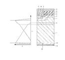
図4は、本発明の第1の実施形態に係る半導体装置(逆阻止IGBT)の活性領域100における電界強度Eを示す特性図である。図4では、図2に示す本発明の第1の実施形態に係る半導体装置(逆阻止IGBT)の活性領域100における、半導体基板底面からの高さyと電界Eとの関係を示す。図2に示す本発明の第1の実施形態に係る半導体装置(逆阻止IGBT)では、逆バイアス時(図4の点線)、n型の高濃度領域5の近傍で空乏層をとめることが可能である。チャネル形成領域2に到達しなければ、n型の高濃度領域5を超えて、チャネル形成領域2側に伸びても良いし、n型の高濃度領域5よりチャネル形成領域2には、電界が及ばないようにすることもできる。一方、順バイアス時(図4の実線)、n型の高濃度領域5によって、ある程度、空乏層の伸び幅が抑制されるが、所定の耐圧を維持することができる。その理由は、上述した条件でn型の高濃度領域5が設けられているからである。
次に、本発明の第1の実施形態に係る半導体装置(逆阻止IGBT)の電流特性について検証した。本発明の第1の実施形態に従い、逆阻止IGBTを準備した(以下、実施例とする)。定格電圧は600Vとした。半導体基板の抵抗率および厚さを、それぞれ30Ωcmおよび100μmとした。つまり、ドリフト領域1の抵抗率を30Ωcmとしている。以下、図5~図9において同様の逆阻止IGBTを用いている。
さらに詳細にn型不純物の総不純物量の与える影響に関して調査した結果を図5から図7に示す。図5は、図2の切断線Y-Yにおける不純物濃度の分布を示す不純物濃度プロファイル図である。実施例の600Vクラス逆阻止IGBTにおいて、半導体基板中の不純物濃度を測定した。この不純物濃度から、n型の高濃度領域5の総ドーズ量を算出した。ここで、n型の高濃度領域5の総ドーズ量とは、n型の高濃度領域5を1回のイオン注入で形成する場合はそのイオン注入のドーズ量であり、複数回のイオン注入によりn型の高濃度領域を形成する場合は各々のイオン注入のドーズ量の総和のことである。
図5において、第1測定結果41は、ドリフト領域1の不純物濃度の分布である。第2測定結果42は、チャネル形成領域2およびボディ領域4の不純物濃度の分布である。第3測定結果43は、第2主電極領域10の不純物濃度の分布である。第4測定結果44は、n型の高濃度領域5の不純物濃度の分布である。これより、n型の高濃度領域5は表面から約10μmの位置に形成されていることがわかる。
さらに詳細にn型不純物の総不純物量の与える影響に関して調査した結果を図5から図7に示す。図5は、図2の切断線Y-Yにおける不純物濃度の分布を示す不純物濃度プロファイル図である。実施例の600Vクラス逆阻止IGBTにおいて、半導体基板中の不純物濃度を測定した。この不純物濃度から、n型の高濃度領域5の総ドーズ量を算出した。ここで、n型の高濃度領域5の総ドーズ量とは、n型の高濃度領域5を1回のイオン注入で形成する場合はそのイオン注入のドーズ量であり、複数回のイオン注入によりn型の高濃度領域を形成する場合は各々のイオン注入のドーズ量の総和のことである。
図5において、第1測定結果41は、ドリフト領域1の不純物濃度の分布である。第2測定結果42は、チャネル形成領域2およびボディ領域4の不純物濃度の分布である。第3測定結果43は、第2主電極領域10の不純物濃度の分布である。第4測定結果44は、n型の高濃度領域5の不純物濃度の分布である。これより、n型の高濃度領域5は表面から約10μmの位置に形成されていることがわかる。
ついで、第4測定結果44の深さごとの不純物濃度を積分し、n型の高濃度領域5の総ドーズ量を算出した。図5に示す不純物濃度の分布は、半導体基板中で、導電型不純物が深さ方向にどのような不純物濃度で存在しているかを示している。図5の第4測定結果44では、基板面に近い領域で不純物濃度が低く、そこから離れるほど不純物濃度が高くなり、再び、不純物濃度が低くなっている。このため、第4測定結果44の深さごとの不純物濃度を積分することで、単位面積当たりのn型の高濃度領域5の総不純物量を算出することができる。つまり、n型の高濃度領域5内の不純物濃度の分布が深さ方向に均一でない場合でも、n型の高濃度領域5全体の総不純物量を算出することができる。このように算出したn型の高濃度領域5の総不純物量から、ドリフト領域1の高濃度領域5部分の総不純物量を減算した値が、n型の高濃度領域5の総ドーズ量となる。
すなわち、図5に示す第4測定結果44の不純物濃度の分布の分布形状内の領域40(図5の斜線部)が、n型の高濃度領域5の総ドーズ量である。ここで、ドリフト領域1の高濃度領域5部分の総不純物量とは、n型の高濃度領域5が設けられる領域中の、ドリフト領域1の総不純物量である。ドリフト領域1の総不純物量は、n型の高濃度領域5と同様の方法で算出している。
すなわち、図5に示す第4測定結果44の不純物濃度の分布の分布形状内の領域40(図5の斜線部)が、n型の高濃度領域5の総ドーズ量である。ここで、ドリフト領域1の高濃度領域5部分の総不純物量とは、n型の高濃度領域5が設けられる領域中の、ドリフト領域1の総不純物量である。ドリフト領域1の総不純物量は、n型の高濃度領域5と同様の方法で算出している。
図6は、n型の高濃度領域5の総ドーズ量と順方向耐圧との関係について示す特性図である。n型の高濃度領域5の総ドーズ量を種々変更し、実施例の逆阻止IGBTを複数準備した。n型の高濃度領域5の総ドーズ量を、それぞれ1×10¹¹~1.2×1012cm-2とし、n型の高濃度領域5の位置は、チャネル形成領域2から10μmの位置とした。そして、それぞれ順方向耐圧を、ゲート-エミッタを短絡した状態で測定した。また、比較として、n型の高濃度領域5が設けられていない逆阻止IGBTを準備し(以下、比較例とする)、順方向耐圧を測定した。図6では、比較例の逆阻止IGBTを、総ドーズ量ゼロとして示している。
図6に示す結果より、n型の高濃度領域5を設けることで、順方向耐圧が低減することがわかった。その理由は、ドリフト領域1のチャネル形成領域2に近い領域にn型の高濃度領域5を設けることで、チャネル形成領域2から第2主電極領域10に向かってドリフト領域1中を伸びる空乏層が短くなるためである。n型の高濃度領域5の総ドーズ量は、4×1011cm-2以下とすることで定格電圧以上を確保可能なことがわかった。
図6に示す結果より、n型の高濃度領域5を設けることで、順方向耐圧が低減することがわかった。その理由は、ドリフト領域1のチャネル形成領域2に近い領域にn型の高濃度領域5を設けることで、チャネル形成領域2から第2主電極領域10に向かってドリフト領域1中を伸びる空乏層が短くなるためである。n型の高濃度領域5の総ドーズ量は、4×1011cm-2以下とすることで定格電圧以上を確保可能なことがわかった。
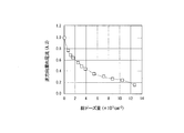
図7は、n型の高濃度領域5の総ドーズ量と逆方向漏れ電流との関係について示す特性図である。図6で用いた実施例の逆阻止IGBTにおいて、逆方向漏れ電流を測定した。図7では、比較例の逆阻止IGBTを、総ドーズ量ゼロとして示している。また、コレクタ-エミッタ電圧を-600Vとし、ゲート-エミッタを短絡した状態で測定した。
図7に示す結果より、n型の高濃度領域5を設けることによって、逆方向漏れ電流が小さくなることがわかった。また、n型の高濃度領域5の総ドーズ量が約4.0×1011cm-2程度までは逆漏れ電流が急激に減少し、4.0×1011cm-2以上では逆漏れ電流の減少が緩やかであることがわかった。
図6および図7の結果より、n型の高濃度領域5の総ドーズ量は4.0×1011cm-2以下で4.0×1011cm-2に近いことが望ましいといえる。
図7に示す結果より、n型の高濃度領域5を設けることによって、逆方向漏れ電流が小さくなることがわかった。また、n型の高濃度領域5の総ドーズ量が約4.0×1011cm-2程度までは逆漏れ電流が急激に減少し、4.0×1011cm-2以上では逆漏れ電流の減少が緩やかであることがわかった。
図6および図7の結果より、n型の高濃度領域5の総ドーズ量は4.0×1011cm-2以下で4.0×1011cm-2に近いことが望ましいといえる。
次に、n型の高濃度領域5の形成領域の与える影響に関して調査した結果を図8および図9に示す。ここでは、耐圧構造領域120をエミッタ電極9と同電位となる引き抜き領域23の外周端からコレクタ電極11と同電位となる分離領域31の内周端までとし、n型の高濃度領域5の端部の位置を耐圧構造領域120に対する相対位置で表した。すなわち、エミッタ電極9と同電位となる引き抜き領域23の外周端部を0、コレクタ電極11と同電位となる分離領域31の内周端を1とした時のn型の高濃度領域5の端部の位置をLとして表した(図3)。従って、n型の高濃度領域5の端部の位置Lが負の値は、活性領域下でn型の高濃度領域5が終わっていることを表し、n型の高濃度領域5の端部の位置Lが1より大きい事は、n型の高濃度領域5が、分離領域31の内周端より外側に張り出していることを表している。
図8は、n型の高濃度領域5の端部の位置Lと、順方向耐圧との関係を示す特性図であり、図9はn型の高濃度領域5の端部の位置Lと逆方向漏れ電流との関係を示す特性図である。ここで、n型の高濃度領域5の総ドーズ量は2×1011cm-2である。また、耐圧構造領域120は上述したように順方向耐圧構造領域121と逆方向耐圧構造領域122からなり、各々、所定の順方向耐圧、逆方向耐圧、および、耐電荷性が得られるように最適化して設計される。
図8より、順方向耐圧はn型の高濃度領域5の端部の位置Lが活性領域端部より活性領域内部あるいはわずかに活性領域側にある時に最も高い値を示している。順方向耐圧が低下し始める位置は、n型の高濃度領域5が引き抜き領域23にかかりはじめる位置であった。また、n型の高濃度領域5を活性領域端部まで設けても順方向耐圧の低下量は1%程度であることがわかった。また、順方向耐圧構造領域121側から耐圧構造領域120の幅Wの36%以上までn型の高濃度領域5を張り出した場合に、順方向耐圧は12%程度まで低下するが、これ以上張り出しても安定した値を取ることがわかった。
図8より、順方向耐圧はn型の高濃度領域5の端部の位置Lが活性領域端部より活性領域内部あるいはわずかに活性領域側にある時に最も高い値を示している。順方向耐圧が低下し始める位置は、n型の高濃度領域5が引き抜き領域23にかかりはじめる位置であった。また、n型の高濃度領域5を活性領域端部まで設けても順方向耐圧の低下量は1%程度であることがわかった。また、順方向耐圧構造領域121側から耐圧構造領域120の幅Wの36%以上までn型の高濃度領域5を張り出した場合に、順方向耐圧は12%程度まで低下するが、これ以上張り出しても安定した値を取ることがわかった。
図9より、逆方向漏れ電流はn型の高濃度領域5の端部の位置Lが活性領域100の端部より内側にあっても低下している。しかし、n型の高濃度領域5が活性領域100の端部から張り出す(Lが+になると)と逆方向漏れ電流の減少量は緩やかになり始める。n型の高濃度領域5を活性領域端部(L=0)まで設けた場合(任意スケールで0.9基準にした場合)の逆方向漏れ電流の低減量は23%((0.9-0.69)/0.9)×100)であり、最大低減量(28%=((0.9-0.65)/0.9)×100))の82%=((23/28)×100)で80%以上であった。また、耐圧構造領域120の幅Wの36%以上になった場合に28%程度減少し、これ以上張り出してもほとんど変化しなくなることが分かった。
図8および図9の結果から、n型の高濃度領域5を活性領域端部まで設けて、端部の位置Lを活性領域の端部を基準(L=0)にして、耐圧構造領域120の幅Wの+10%から-10%の範囲にすることで、順方向耐圧の低下量を抑制しながら、逆方向漏れ電流の低減を図ることができる。さらに、好ましくは、耐圧構造領域120の幅Wの+5%から-5%の範囲にするとよい。
また、n型の高濃度領域5の端部の位置Lを耐圧構造領域120の幅Wの36%以上とすることで、n型の高濃度領域5の幅がばらついた場合でも、安定的に順方向耐圧と逆方向漏れ電流を維持できる。
また、n型の高濃度領域5の端部の位置Lを耐圧構造領域120の幅Wの36%以上とすることで、n型の高濃度領域5の幅がばらついた場合でも、安定的に順方向耐圧と逆方向漏れ電流を維持できる。
以上、説明したように、本発明の第1の実施形態に係る半導体装置(逆阻止IGBT)によれば、第1主電極領域(エミッタ領域)3と第2主電極領域(コレクタ領域)10との間におけるドリフト領域1のチャネル形成領域(ベース領域)2に近い領域に、所定の濃度のn型の高濃度領域5を設けることで、所定の順方向耐圧を維持したままで、逆方向漏れ電流を低減することが可能となる。実施例では、図6に示すように、n型の高濃度領域5中のn型不純物の総ドーズ量が4.0×1011cm-2となる不純物濃度を有するn型の高濃度領域5を設けることで、n型の高濃度領域5を設けない場合に対して、順方向耐圧が600Vで、逆方向漏れ電流を約60%低減することが可能である。
また、第2主電極領域(コレクタ領域)10から、チャネル形成領域2に向かって空乏層が伸びた場合に、n型の高濃度領域5とチャネル形成領域2の間に中性領域が残り過剰キャリアの残留することでソフトリカバリーとなり、逆回復時の電圧・電流波形の振動が抑制される。
また、n型の高濃度領域5を活性領域100の端部まで設けることで、順方向耐圧の低下量を抑制しながら、逆方向漏れ電流を低減することが可能であることが分かった。また、n型の高濃度領域5を耐圧構造領域120の幅Wの36%以上まで設けることで、n型の高濃度領域5の幅がばらついた場合でも、安定的に順方向耐圧と逆方向漏れ電流が得られることがわかった。
また、n型の高濃度領域5を活性領域100の端部まで設けることで、順方向耐圧の低下量を抑制しながら、逆方向漏れ電流を低減することが可能であることが分かった。また、n型の高濃度領域5を耐圧構造領域120の幅Wの36%以上まで設けることで、n型の高濃度領域5の幅がばらついた場合でも、安定的に順方向耐圧と逆方向漏れ電流が得られることがわかった。
尚、ドリフト領域1は、定格電圧と等しい逆方向電圧が印加された時、第2主電極領域10から引き抜き領域23(引き抜き領域)に向かって拡がる空乏層がこの引き抜き領域に到達しない抵抗率を有するようにする。
以上、実施例の説明では、プレーナーゲート型逆阻止IGBTをモデルとしたが、ゲート電極がドリフト領域1に形成された溝内に埋設されているトレンチゲート型逆阻止IGBTであってもかまわない。また、本発明では、n型とp型をすべて逆転した構成としてもよい。
尚、上述のn型の高濃度領域5は、例えば、選択的なプロトン照射と熱処理によるドナー化によって形成することができる。
以上、実施例の説明では、プレーナーゲート型逆阻止IGBTをモデルとしたが、ゲート電極がドリフト領域1に形成された溝内に埋設されているトレンチゲート型逆阻止IGBTであってもかまわない。また、本発明では、n型とp型をすべて逆転した構成としてもよい。
尚、上述のn型の高濃度領域5は、例えば、選択的なプロトン照射と熱処理によるドナー化によって形成することができる。
(第2の実施形態)
本発明の第2の実施形態に係る半導体装置を、図10を用いて説明する。図10は、図2に相当する断面図であり、図1のプレーナゲート型の逆阻止IGBTの活性領域100をトレンチゲート型IGBTにした場合の活性領域の構成を示す断面図である。
図10に示すように、本発明の第2の実施形態に係る半導体装置は、第1導電型(n-型)のドリフト領域1aとなる半導体基板を主体にしたトレンチゲート型の逆阻止IGBTである。また、本発明の第2の実施形態に係る半導体装置(逆阻止IGBT)は、詳細に図示していないが、本発明の第1の実施形態に係る半導体装置と同様に、ドリフト領域1aとなる半導体基板上に、図1に示す活性領域100と、活性領域100の外側に設けられた耐圧構造領域120と、耐圧構造領域120の外側に設けられた分離部130とを備えている。
本発明の第2の実施形態に係る半導体装置を、図10を用いて説明する。図10は、図2に相当する断面図であり、図1のプレーナゲート型の逆阻止IGBTの活性領域100をトレンチゲート型IGBTにした場合の活性領域の構成を示す断面図である。
図10に示すように、本発明の第2の実施形態に係る半導体装置は、第1導電型(n-型)のドリフト領域1aとなる半導体基板を主体にしたトレンチゲート型の逆阻止IGBTである。また、本発明の第2の実施形態に係る半導体装置(逆阻止IGBT)は、詳細に図示していないが、本発明の第1の実施形態に係る半導体装置と同様に、ドリフト領域1aとなる半導体基板上に、図1に示す活性領域100と、活性領域100の外側に設けられた耐圧構造領域120と、耐圧構造領域120の外側に設けられた分離部130とを備えている。
耐圧構造領域の構成は、上述のプレーナゲート型の逆阻止IGBTと同様である。活性領域100には、第1導電型(n-型)のドリフト領域1aとなる半導体基板のおもて面(ドリフト領域1aの第1主面Y1)に、複数のトレンチ溝12が所定の間隔で設けられている。半導体基板のおもて面の表面層には、第2導電型(p型)のチャネル形成領域2aがトレンチ溝12に挟まれるように設けられている。p型のチャネル形成領域2aは、n-型のドリフト領域1aよりも高い不純物濃度を有する。隣り合うトレンチ溝12に挟まれた部分においてp型のチャネル形成領域2aの基板おもて面側の表面層には、第1導電型(n+型)の第1主電極領域3aおよび第2導電型(p+型)のボディ領域4aが選択的に設けられる。p+型のボディ領域4aは、p型のチャネル形成領域2aよりも高い不純物濃度を有する。p型のチャネル形成領域2aの、隣り合うトレンチ溝12に挟まれた部分には、n+型の第1主電極領域3aおよびp+型のボディ領域4aが設けられた構成の部分と、この構成からn+型の第1主電極領域3aがない構成の部分とが交互に並んで設けられている。
n型の高濃度領域5は、n-型のドリフト領域1aとp型のチャネル形成領域2aとの間の表面に近い領域に設けられる。第2電極としてのエミッタ電極9aは、n+型の第1主電極領域3aおよびp+型のボディ領域4aの表面に共通に接する。また、エミッタ電極9aは、層間絶縁膜8aによって第1電極としてのゲート電極7aとは電気的に絶縁されている。
ドリフト領域1の第2主面2Yには、コレクタ領域としての第2主電極領域10aが設けられている。この第2主電極領域10aには、ドリフト領域1の第2主面2Y側(半導体基板の裏面)に設けられた第3電極としてのコレクタ電極11aが接している。
ドリフト領域1の第2主面2Yには、コレクタ領域としての第2主電極領域10aが設けられている。この第2主電極領域10aには、ドリフト領域1の第2主面2Y側(半導体基板の裏面)に設けられた第3電極としてのコレクタ電極11aが接している。
前述のトレンチ溝12の構造について、さらに説明する。トレンチ溝12は、n+型の第1主電極領域3aおよびp型のチャネル形成領域2aを貫通する深さを必ず必要とするが、前述のn型の高濃度領域5に対しては、このn型の高濃度領域5の中間の深さでも、貫通する深さであっても、到達しない深さであってもよい。トレンチ溝12内に形成されるMOSゲート構造(トレンチゲートMOS構造)は、従来と同様に、トレンチ溝12の内壁に沿って絶縁膜としてのゲート絶縁膜6aが設けられ、トレンチ溝12の内部にゲート絶縁膜6aを介してポリシリコンからなる第1電極としてのゲート電極7aが埋設される構造である。
本発明の第2の実施形態に係る半導体装置では、トレンチゲート型IGBTの表面構造として、隣り合うトレンチ溝12に挟まれた部分には、n+型の第1主電極領域3aおよびp+型のボディ領域4aが設けられた構成の部分と、この構成からn+型の第1主電極領域3aがない構成の部分とが交互に並んで設けられている例をあげたが、トレンチゲートが形成されていれば、他の構成のトレンチゲート型IGBTであってもn型の高濃度領域5を形成した場合の効果を得ることができる。
以上のように、本発明にかかる半導体装置は、例えばマトリックスコンバータなどの直列変換回路に用いられるスイッチなど、順方向および逆方向の電圧に対する耐圧特性が要求される半導体素子に有用である。
1 ドリフト領域
2 チャネル形成領域
3 第1主電極領域
5 高濃度領域
6 ゲート絶縁膜
7 ゲート電極
8 層間絶縁膜
9 エミッタ電極
10 第2主電極領域
11 コレクタ電極
23 引き抜き領域
31 分離領域
100 活性領域
120 耐圧構造領域
121 順方向耐圧構造領域
122 逆方向耐圧構造領域
130 分離部
2 チャネル形成領域
3 第1主電極領域
5 高濃度領域
6 ゲート絶縁膜
7 ゲート電極
8 層間絶縁膜
9 エミッタ電極
10 第2主電極領域
11 コレクタ電極
23 引き抜き領域
31 分離領域
100 活性領域
120 耐圧構造領域
121 順方向耐圧構造領域
122 逆方向耐圧構造領域
130 分離部
Claims (9)
- 互いに反対側に位置する第1主面及び第2主面を有する第1導電型のドリフト領域と、
前記ドリフト領域の第1主面に選択的に設けられた第2導電型のチャネル形成領域と、
前記チャネル形成領域の上部に選択的に設けられた第1導電型の第1主電極領域と、
前記ドリフト領域の第2主面に設けられた第2導電型の第2主電極領域と、
前記チャネル形成領域の下の前記ドリフト領域に前記チャネル形成領域から離れて設けられた第1導電型の高濃度領域と、
前記ドリフト領域の外周であって前記チャネル形成領域を取り囲むように設けられ、前記第1主電極領域に接続された第2導電型の引き抜き領域と、
前記引き抜き領域の外周であって前記引き抜き領域を取り囲むように設けられ、順方向耐圧構造と逆方向耐圧構造とを含む耐圧構造領域と、
前記耐圧構造領域の外周であって、前記ドリフト領域の外周端部に設けられ、前記ドリフト領域の第1主面から第2主面まで貫通し、前記第2主電極領域に接する第2導電型の分離領域と、を備え、
前記高濃度領域は、前記ドリフト領域よりも高い不純物濃度であり、かつ、前記高濃度領域中の第1導電型不純物の総不純物量が2.0×1012cm-2以下となる不純物濃度を有することを特徴とする半導体装置。 - 前記第1主電極領域から前記ドリフト領域の第1主面に跨るように、絶縁膜を介して設けられた第1電極と、
前記チャネル形成領域および前記第1主電極領域に接続された第2電極と、
前記第1主電極領域に接する第3電極と、を更に備えることを特徴とする請求項1に記載の半導体装置。 - 前記チャネル形成領域の上部から前記チャネル形成領域を貫通し、前記ドリフト領域に達するように形成された溝と、
前記溝内に絶縁膜を介して埋設された第1電極と、
前記チャネル形成領域および前記第1主電極領域に接続された第2電極と、
前記第2主電極領域に接する第3電極と、を更に備えることを特徴とする請求項1に記載の半導体装置。 - 前記高濃度領域は、前記ドリフト領域よりも高い不純物濃度であり、かつ、前記高濃度領域中の第1導電型不純物の総ドーズ量が4.0×1011cm-2以下となる不純物濃度を有することを特徴とする請求項1乃至3の何れか1項に記載の半導体装置。
- 前記高濃度領域の端部が、前記引き抜き領域の外周端を基準にして前記耐圧構造領域の長さの+10%~-10%の範囲にあることを特徴とする請求項1乃至3の何れか1項に記載の半導体装置。
- 前記高濃度領域の端部が、前記引き抜き領域の外周端を基準にして前記耐圧構造領域の長さの+5%~-5%の範囲にあることを特徴とする請求項1乃至3の何れか1項に記載の半導体装置。
- 前記高濃度領域の端部が、前記引き抜き領域の外周端を基準にして前記耐圧構造領域の長さの+36%以上にあることを特徴とする請求項1乃至3の何れか1項に記載の半導体装置。
- 前記耐圧構造領域の前記ドリフト領域の表面に、前記引き抜き領域を囲むように互いに離れて設けられた複数の第2導電型のフィールドリミッティングリング領域を備えることを特徴とする請求項1乃至3の何れか1項に記載の半導体装置。
- 前記ドリフト領域は、定格電圧と等しい逆方向電圧が印加された時、前記第2主電極領域から前記引き抜き領域に向かって拡がる空乏層が前記引き抜き領域に到達しない抵抗率を有することを特徴とする請求項1乃至請求項3の何れか1項に記載の半導体装置。
Priority Applications (2)
| Application Number | Priority Date | Filing Date | Title |
|---|---|---|---|
| JP2015527169A JP6052413B2 (ja) | 2013-07-17 | 2014-07-09 | 半導体装置 |
| US14/824,013 US9577088B2 (en) | 2013-07-17 | 2015-08-11 | Semiconductor device with high concentration region |
Applications Claiming Priority (2)
| Application Number | Priority Date | Filing Date | Title |
|---|---|---|---|
| JP2013148334 | 2013-07-17 | ||
| JP2013-148334 | 2013-07-17 |
Related Child Applications (1)
| Application Number | Title | Priority Date | Filing Date |
|---|---|---|---|
| US14/824,013 Continuation US9577088B2 (en) | 2013-07-17 | 2015-08-11 | Semiconductor device with high concentration region |
Publications (1)
| Publication Number | Publication Date |
|---|---|
| WO2015008458A1 true WO2015008458A1 (ja) | 2015-01-22 |
Family
ID=52345938
Family Applications (1)
| Application Number | Title | Priority Date | Filing Date |
|---|---|---|---|
| PCT/JP2014/003649 Ceased WO2015008458A1 (ja) | 2013-07-17 | 2014-07-09 | 半導体装置 |
Country Status (3)
| Country | Link |
|---|---|
| US (1) | US9577088B2 (ja) |
| JP (1) | JP6052413B2 (ja) |
| WO (1) | WO2015008458A1 (ja) |
Cited By (3)
| Publication number | Priority date | Publication date | Assignee | Title |
|---|---|---|---|---|
| JP2017063174A (ja) * | 2015-09-24 | 2017-03-30 | 豊田合成株式会社 | 半導体装置および電力変換装置 |
| US10468515B2 (en) | 2015-09-24 | 2019-11-05 | Toyoda Gosei Co., Ltd. | Semiconductor device and power converter |
| CN119545827A (zh) * | 2024-12-24 | 2025-02-28 | 海信家电集团股份有限公司 | Rc-igbt结构及半导体器件 |
Families Citing this family (3)
| Publication number | Priority date | Publication date | Assignee | Title |
|---|---|---|---|---|
| JP6676988B2 (ja) | 2016-01-29 | 2020-04-08 | 株式会社デンソー | 半導体装置 |
| CN117673163B (zh) * | 2024-02-01 | 2024-06-07 | 深圳天狼芯半导体有限公司 | 高短路耐量的超结mosfet及其制备方法、芯片 |
| CN119092488B (zh) * | 2024-11-06 | 2025-04-01 | 杭州士兰集昕微电子有限公司 | 半导体器件及其制造方法、半导体器件的设计方法 |
Citations (2)
| Publication number | Priority date | Publication date | Assignee | Title |
|---|---|---|---|---|
| JP2005101551A (ja) * | 2003-08-29 | 2005-04-14 | Fuji Electric Holdings Co Ltd | 半導体装置とその製造方法およびその半導体装置を用いた双方向スイッチ素子 |
| JP2009188336A (ja) * | 2008-02-08 | 2009-08-20 | Fuji Electric Device Technology Co Ltd | 半導体装置およびその製造方法 |
Family Cites Families (14)
| Publication number | Priority date | Publication date | Assignee | Title |
|---|---|---|---|---|
| JP3458590B2 (ja) | 1996-03-27 | 2003-10-20 | 富士電機株式会社 | 絶縁ゲートバイポーラトランジスタ |
| JP3395520B2 (ja) | 1996-06-04 | 2003-04-14 | 富士電機株式会社 | 絶縁ゲートバイポーラトランジスタ |
| WO2000035021A1 (de) | 1998-12-04 | 2000-06-15 | Infineon Technologies Ag | Leistungshalbleiterschalter |
| JP4967200B2 (ja) | 2000-08-09 | 2012-07-04 | 富士電機株式会社 | 逆阻止型igbtを逆並列に接続した双方向igbt |
| JP4904625B2 (ja) | 2001-02-14 | 2012-03-28 | 富士電機株式会社 | 半導体装置 |
| JP4539011B2 (ja) * | 2002-02-20 | 2010-09-08 | 富士電機システムズ株式会社 | 半導体装置 |
| US7157785B2 (en) * | 2003-08-29 | 2007-01-02 | Fuji Electric Device Technology Co., Ltd. | Semiconductor device, the method of manufacturing the same, and two-way switching device using the semiconductor devices |
| JP4843923B2 (ja) | 2004-09-09 | 2011-12-21 | 富士電機株式会社 | 高耐圧半導体装置およびその製造方法 |
| JP5104314B2 (ja) | 2005-11-14 | 2012-12-19 | 富士電機株式会社 | 半導体装置およびその製造方法 |
| JP5034315B2 (ja) | 2006-05-19 | 2012-09-26 | 三菱電機株式会社 | 半導体装置及びその製造方法 |
| JP2008258262A (ja) | 2007-04-02 | 2008-10-23 | Toyota Motor Corp | Igbt |
| JP5358963B2 (ja) | 2008-02-04 | 2013-12-04 | 富士電機株式会社 | 半導体装置およびその製造方法 |
| DE102010063728B4 (de) | 2009-12-28 | 2016-04-14 | Fuji Electric Co., Ltd. | Halbleitervorrichtung mit verbesserter Sperrspannungsfestigkeit |
| JP2014086600A (ja) * | 2012-10-24 | 2014-05-12 | Fuji Electric Co Ltd | 半導体装置、半導体装置の製造方法および半導体装置の制御方法 |
-
2014
- 2014-07-09 WO PCT/JP2014/003649 patent/WO2015008458A1/ja not_active Ceased
- 2014-07-09 JP JP2015527169A patent/JP6052413B2/ja active Active
-
2015
- 2015-08-11 US US14/824,013 patent/US9577088B2/en active Active
Patent Citations (2)
| Publication number | Priority date | Publication date | Assignee | Title |
|---|---|---|---|---|
| JP2005101551A (ja) * | 2003-08-29 | 2005-04-14 | Fuji Electric Holdings Co Ltd | 半導体装置とその製造方法およびその半導体装置を用いた双方向スイッチ素子 |
| JP2009188336A (ja) * | 2008-02-08 | 2009-08-20 | Fuji Electric Device Technology Co Ltd | 半導体装置およびその製造方法 |
Cited By (3)
| Publication number | Priority date | Publication date | Assignee | Title |
|---|---|---|---|---|
| JP2017063174A (ja) * | 2015-09-24 | 2017-03-30 | 豊田合成株式会社 | 半導体装置および電力変換装置 |
| US10468515B2 (en) | 2015-09-24 | 2019-11-05 | Toyoda Gosei Co., Ltd. | Semiconductor device and power converter |
| CN119545827A (zh) * | 2024-12-24 | 2025-02-28 | 海信家电集团股份有限公司 | Rc-igbt结构及半导体器件 |
Also Published As
| Publication number | Publication date |
|---|---|
| JP6052413B2 (ja) | 2016-12-27 |
| JPWO2015008458A1 (ja) | 2017-03-02 |
| US20150349111A1 (en) | 2015-12-03 |
| US9577088B2 (en) | 2017-02-21 |
Similar Documents
| Publication | Publication Date | Title |
|---|---|---|
| JP5981859B2 (ja) | ダイオード及びダイオードを内蔵する半導体装置 | |
| JP5754543B2 (ja) | 半導体装置 | |
| JP6416062B2 (ja) | 半導体装置 | |
| US9082815B2 (en) | Semiconductor device having carrier extraction in electric field alleviating layer | |
| JP5748188B2 (ja) | 半導体装置 | |
| JP3979258B2 (ja) | Mis半導体装置およびその製造方法 | |
| JP7118033B2 (ja) | 半導体装置 | |
| JP5753814B2 (ja) | ダイオード、半導体装置およびmosfet | |
| JP6052413B2 (ja) | 半導体装置 | |
| JP2013051345A (ja) | ダイオード、半導体装置およびmosfet | |
| JP2018152426A (ja) | 半導体装置 | |
| US10490655B2 (en) | Insulated gate bipolar transistor (IGBT) with high avalanche withstand | |
| JP6918736B2 (ja) | 半導体装置 | |
| CN104900699A (zh) | 半导体装置 | |
| JP7169459B2 (ja) | スイッチング素子 | |
| JP2013251468A (ja) | 半導体装置および半導体装置の制御方法 | |
| WO2015107614A1 (ja) | 電力用半導体装置 | |
| KR20150069117A (ko) | 전력 반도체 소자 | |
| US20150144993A1 (en) | Power semiconductor device | |
| JP2021034528A (ja) | スイッチング素子 | |
| JP7010095B2 (ja) | 半導体装置 | |
| JP6754310B2 (ja) | 半導体装置 | |
| JP6754308B2 (ja) | 半導体装置 | |
| JP2014212252A (ja) | 半導体装置 | |
| JP2013069801A (ja) | 半導体装置 |
Legal Events
| Date | Code | Title | Description |
|---|---|---|---|
| 121 | Ep: the epo has been informed by wipo that ep was designated in this application |
Ref document number: 14826339 Country of ref document: EP Kind code of ref document: A1 |
|
| ENP | Entry into the national phase |
Ref document number: 2015527169 Country of ref document: JP Kind code of ref document: A |
|
| NENP | Non-entry into the national phase |
Ref country code: DE |
|
| 122 | Ep: pct application non-entry in european phase |
Ref document number: 14826339 Country of ref document: EP Kind code of ref document: A1 |