WO2014208412A1 - Élément optique - Google Patents
Élément optique Download PDFInfo
- Publication number
- WO2014208412A1 WO2014208412A1 PCT/JP2014/066122 JP2014066122W WO2014208412A1 WO 2014208412 A1 WO2014208412 A1 WO 2014208412A1 JP 2014066122 W JP2014066122 W JP 2014066122W WO 2014208412 A1 WO2014208412 A1 WO 2014208412A1
- Authority
- WO
- WIPO (PCT)
- Prior art keywords
- refractive index
- layer
- multilayer film
- film
- back surface
- Prior art date
Links
Images


Classifications
-
- G—PHYSICS
- G02—OPTICS
- G02B—OPTICAL ELEMENTS, SYSTEMS OR APPARATUS
- G02B1/00—Optical elements characterised by the material of which they are made; Optical coatings for optical elements
- G02B1/10—Optical coatings produced by application to, or surface treatment of, optical elements
- G02B1/11—Anti-reflection coatings
- G02B1/113—Anti-reflection coatings using inorganic layer materials only
- G02B1/115—Multilayers
-
- G—PHYSICS
- G02—OPTICS
- G02B—OPTICAL ELEMENTS, SYSTEMS OR APPARATUS
- G02B5/00—Optical elements other than lenses
- G02B5/20—Filters
- G02B5/28—Interference filters
- G02B5/283—Interference filters designed for the ultraviolet
-
- G—PHYSICS
- G02—OPTICS
- G02C—SPECTACLES; SUNGLASSES OR GOGGLES INSOFAR AS THEY HAVE THE SAME FEATURES AS SPECTACLES; CONTACT LENSES
- G02C7/00—Optical parts
- G02C7/02—Lenses; Lens systems ; Methods of designing lenses
-
- G—PHYSICS
- G02—OPTICS
- G02C—SPECTACLES; SUNGLASSES OR GOGGLES INSOFAR AS THEY HAVE THE SAME FEATURES AS SPECTACLES; CONTACT LENSES
- G02C2202/00—Generic optical aspects applicable to one or more of the subgroups of G02C7/00
- G02C2202/16—Laminated or compound lenses
Definitions
- the present invention relates to an optical component such as a spectacle lens.
- plastic lenses are frequently used for spectacle lenses because of their advantages of being lightweight, excellent in impact resistance and easy to dye.
- plastic lenses used for spectacle lenses are usually provided with antireflection films on both sides.
- antireflection films for spectacle lenses generally have low reflection characteristics (broadband low reflection characteristics) over the entire visible region of 380 nm to 780 nm.
- ultraviolet rays of 280 nm to 380 nm are known to cause damage to the retina due to exposure to the eyeball. It is considered desirable to cut off light in the ultraviolet region because long-term exposure to ultraviolet rays outdoors causes keratitis, cataracts, and the like.
- dyed lenses such as sunglasses are known.
- some spectacle lenses contain a UV absorber in the lens body and some are provided with UV cut coating. . In such sunglasses and conventional spectacle lenses, it is possible to reduce or block ultraviolet rays incident from the front surface (front surface; the surface opposite to the eyeball) of the spectacle lens.
- Patent Document 1 discloses a spectacle lens in which an inorganic film having a surface reflectance smaller than that of the lens base material itself is formed on the back surface of the spectacle lens with respect to all rays in the wavelength region of 280 to 315 nm and 420 to 680 nm. It is disclosed.
- the spectacle lens disclosed in Patent Document 1 it is possible to reliably prevent ultraviolet rays from the rear in the line of sight, particularly far ultraviolet rays, from being reflected from the back surface of the lens, thereby reducing the amount of ultraviolet rays entering the eye. It is said.
- Patent Document 2 discloses a multilayer structure comprising a laminated body of at least one high refractive index layer having a refractive index of 1.6 or more and at least one low refractive index layer having a refractive index of 1.5 or less on the back surface of the spectacle lens.
- An eyeglass lens having an antireflection film which has an average reflectance Rm in the visible range of 1.15% or less, a luminous reflectance Rv of 1% or less, and incident angles of 30 ° and 45 °,
- the weighted average reflectance Ruv (ISO 13666: 1998 Standard) in the wavelength region of 380 nm is 5% or less
- the multilayer film is 3 to 7 layers
- the outer layer of the multilayer film is An eyeglass lens that is a silica-based film is disclosed.
- ultraviolet and antireflection films having good antireflection performance in the visible region and the ultraviolet region are formed on the back surface of the lens.
- the present invention has been made in view of the above circumstances, and an object of the present invention is to provide an optical component that is effective in preventing eye diseases and has good visibility. That is, the object of the present invention is to eliminate the above-mentioned problems of the prior art, suppress degradation of performance such as heat resistance, crack resistance and durability, and prevent reflection in the ultraviolet region without any deterioration in optical performance in the visible region. It is to provide an optical component with excellent performance.
- an optical component of the present invention is an optical component including a multilayer film on at least the back surface of a plastic lens, and the multilayer film disposed on the back surface of the plastic lens has an incident angle.
- the average reflectance in the wavelength region of 280 nm to 380 nm at 0 ° to 45 ° is 15% or less
- the multilayer film disposed on the back surface includes a high refractive index layer made of a high refractive index material and a low refractive index.
- the optical film thickness of the at least one high refractive index layer in the multilayer film disposed on the back surface is three or more layers with a low refractive index layer made of a refractive index material. It is a thick film having a thickness of 0.700 ⁇ .
- the ratio of the high refractive index layer to the total film thickness of the multilayer film disposed on the back surface is preferably greater than 45%.
- the multilayer film disposed on the back surface preferably has an average reflectance of 10% or less in a wavelength region of 280 nm to 380 nm when the incident angle is 0 degree to 45 degrees. Further, it is preferable that a luminous reflectance of reflected light of the multilayer film disposed on the back surface is 1.5% or less and a hue angle thereof is 120 to 220 degrees.
- the one high refractive index layer that is the thick film is a layer farthest from the base material of the plastic lens among the high refractive index layers in the multilayer film disposed on the back surface.
- a conductor film, a metal film, or a visible light absorbing film is provided between the high refractive index layer and the low refractive index layer constituting the multilayer film disposed on the back surface.
- the plastic lens preferably has a function of absorbing ultraviolet rays.
- the base material of the plastic lens may be colored.
- the transmittance of the colored plastic lens substrate is preferably 5 to 85%.
- the spectral characteristic curve representing the reflectance of the multilayer film disposed on the back surface with respect to the wavelength is a curve having one extreme value or a monotone having no extreme value.
- the spectral characteristic curve is a curve having the one extreme value
- the one extreme value is preferably a reflectance of 20% or less.
- the multilayer film may be disposed on the surface of the plastic lens in addition to the back surface of the plastic lens.
- the optical multilayer film configured as described above can obtain a sufficient ultraviolet ray cutting effect while maintaining good visibility without changing in the characteristics of the visible region as compared with the conventional spectacle lens.
- it since it is configured as described above, it suppresses deterioration of performance such as heat resistance, crack resistance and durability, and does not deteriorate optical performance in the visible region, and prevents reflection in the ultraviolet region.
- An optical component having excellent performance can be provided.
- it is possible to provide an optical component having reduced optical intensity in the eyeball, reduced glare, easy to see, and effective optical properties for fatigue and eye disease prevention. It becomes.
- 10 is a graph showing a spectral characteristic curve of a multilayer film on the back surface of the lens of Example 3.
- 6 is a graph showing a spectral characteristic curve of a multilayer film on the back surface of the lens of Example 4.
- 6 is a graph showing a spectral characteristic curve of a multilayer film on the back surface of the lens of Example 5.
- 14 is a graph showing a spectral characteristic curve of a multilayer film on the back surface of the lens of Example 6.
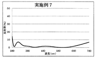
- 10 is a graph showing a spectral characteristic curve of a multilayer film on the back surface of the lens of Example 7.
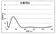
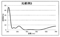
- 6 is a graph showing a spectral characteristic curve of a multilayer film on the back surface of the lens of Comparative Example 1; 6 is a graph showing a spectral characteristic curve of a multilayer film on the back surface of the lens of Comparative Example 2. 10 is a graph showing a spectral characteristic curve of a multilayer film on the back surface of the lens of Comparative Example 3.
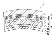
- FIG. 1 is a sectional side view which shows typically an example of the optical component which concerns on 1st Embodiment of this invention.
- An optical component 1 shown in FIG. 1 is an optical component for a spectacle lens, and includes a plastic substrate 2 and an inorganic multilayer film 3 disposed on the back surface of the plastic substrate 2.
- a functional thin film 4 is disposed between the back surface of the plastic substrate 2 and the inorganic multilayer film 3, and the functional thin film 4 includes a primer layer 5 and a hard coat layer. It consists of six.
- a water / oil repellent film 12 is further provided on the inorganic multilayer film 3. The water / oil repellent film 12 will be described later.
- arbitrary films corresponding to the inorganic multilayer film 3 and the functional thin film 4 are also formed on the surface of the plastic substrate 2, but illustration and description of such films are omitted.
- the plastic substrate 2 is, for example, a transparent plastic such as acrylic resin, thiourethane resin, methacrylic resin, allyl resin, episulfide resin, polycarbonate resin, polyurethane resin, polyester resin, polystyrene resin, episulfide. Resin, polyethersulfone resin poly-4-methylpentene-1 resin, diethylene glycol bisallyl carbonate resin (CR-39), polyvinyl chloride resin, halogen-containing copolymer, sulfur-containing copolymer, etc. is there.
- the refractive index (nd) of the plastic substrate 2 is selected from, for example, 1.50, 1.60, 1.67, and 1.74.
- the plastic substrate 2 When the refractive index of the plastic substrate 2 is 1.6 or more, it is preferable to use an allyl carbonate resin, an acrylate resin, a methacrylate resin, a thiourethane resin, or the like as the plastic substrate 2. .
- the plastic substrate 2 preferably has a function of absorbing ultraviolet rays. That is, it is preferable that the resin constituting the plastic substrate 2 contains an ultraviolet absorber.
- the functional thin film 4 disposed on the surface of the plastic substrate 2 may contain an ultraviolet absorber. In such a case, the plastic substrate 2 is impregnated with the ultraviolet absorbent component in the functional thin film 4.
- the plastic substrate 2 may not be transparent as long as it has translucency, and may be colored.
- the transmittance of the colored plastic substrate 2 is preferably 5 to 85%.
- the functional thin film 4 is disposed between the plastic substrate 2 and the inorganic multilayer film 3 as described above, and a primer layer 5 disposed in contact with the plastic substrate 2, and the primer layer 5 And a hard coat layer 6 disposed in contact with the inorganic multilayer film 3.
- the primer layer 5 is for improving the adhesion between the plastic substrate 2 and the hard coat layer 6 and functions as an adhesion layer. Moreover, it is also for absorbing the impact on the optical component 1 and functions as an impact absorbing layer.
- the primer layer 5 is mainly composed of a polyurethane-based resin, and in this embodiment, the polyurethane-based resin contains, for example, fine particles of an inorganic material.
- the primer layer 5 may contain at least one of acrylic resin, methacrylic resin, and organosilicon resin.
- the thickness (actual thickness) of the primer layer 5 is preferably about 0.5 ⁇ m or more and 1.0 ⁇ m or less.
- Such a primer layer 5 can be formed on the plastic substrate 2 with a predetermined thickness by immersing the plastic substrate 2 in a material solution for forming the primer layer 5 and then lifting and drying.
- a material for forming the primer layer 5 for example, a liquid obtained by dispersing or dissolving the above-described resin and the inorganic oxide fine particle sol in water or an alcohol solvent and mixing them can be used.
- the hard coat layer 6 has a function of protecting the plastic substrate 2 and suppressing damage to the plastic substrate 2, and functions as a scratch-resistant film.
- the hard coat layer 6 is made of, for example, an organosiloxane hard coat layer.
- the organosiloxane hard coat layer is obtained by dispersing inorganic oxide fine particles in an organosiloxane resin.
- the inorganic oxide for example, rutile type titanium oxide, oxides of silicon, tin, zirconium, and antimony are preferably used.
- the hard coat layer 6 may be an organic silicon-based resin containing colloidal silica as disclosed in, for example, Japanese Patent Publication No. 4-55615.
- the thickness (actual thickness) of the hard coat layer 6 is preferably about 2 ⁇ m to 4 ⁇ m.
- the hard coat layer 6 is formed on the primer layer 5 on the plastic substrate 2 by immersing the plastic substrate 2 on which the primer layer 5 is formed in the forming material solution of the hard coat layer 6 and then lifting and drying. It can be formed with a thickness of As the forming material liquid for the hard coat layer 6, for example, a liquid obtained by dispersing or dissolving the above-described resin to be the hard coat layer 6 and the inorganic oxide fine particle sol in water or an alcohol-based solvent can be used. .
- the interface between the functional thin film 4 and the plastic substrate 2 is sufficient if the refractive index and the refractive index of the plastic substrate 2 are substantially the same. Generation of interference fringes caused by reflection on the surface and a decrease in transmittance can be suppressed. Therefore, it is desirable to adjust the refractive index of the functional thin film 4 in accordance with the refractive index of the plastic substrate 2.
- the type (physical properties) of the resin that is the main component of the functional thin film 4 is selected, or the resin that is the main component This can be done by selecting the type (physical properties) of the fine particles to be added.
- the functional thin film 4 is formed including the primer layer 5 and the hard coat layer 6.
- the primer layer 5 and the hard coat layer 6 are formed. It may be omitted.
- a conductor film made of ITO (Indium Tin Oxide) a metal film such as Ni, Cr, or a visible light absorption layer
- the above-described primer layer 5 and hard coat layer 6 are used. In addition to this, it may be arranged.
- a conductive film such as ITO or a metal film such as Ni or Cr having a thickness of 20 nm or less between the high refractive index inorganic material and the low refractive index inorganic material constituting the inorganic multilayer film 3.
- a visible light absorption film or the like may be provided.
- the thickness of the conductor film, metal film or visible light may be 10 nm or less.
- the conductor film, the metal film, or the visible light absorption film is more electrically conductive than the oxide that is a high refractive index inorganic material used in the multilayer film of the present invention, and also absorbs visible light.
- the inorganic multilayer film 3 has a multilayer structure in which a plurality of high refractive index inorganic materials (high refractive index substances) and low refractive index inorganic materials (low refractive index substances) are alternately stacked on the plastic substrate 2 described above.
- the antireflection film has a multilayer structure in which a high refractive index layer made of a high refractive index material and a low refractive index layer made of a low refractive index material are stacked in three or more layers, and prevents reflection of incident light. It has the function as.
- the inorganic multilayer film 3 is designed so that the average reflectance in the wavelength region (ultraviolet region) of 280 nm to 380 nm when the incident angle is 0 degree to 45 degrees is 15% or less.
- the average reflectance in the ultraviolet region is preferably 10% or less, for example, the average reflectance in the ultraviolet region when the incident angle is 0 degrees is 4% or more, and the ultraviolet region when the incident angle is 45 degrees.
- An average reflectance of 2.5% or more is particularly preferable.
- the reason why the average reflectance in the ultraviolet region is limited to 15% or less is that when the average reflectance is set to 15% or less, the light in the ultraviolet region can be sufficiently cut, and when used as a spectacle lens, A filter function such as a sufficient antiglare effect can be obtained while maintaining good visibility, and ultraviolet rays incident on the eyeball can be reduced.
- the average reflectance in the ultraviolet region is set to more than 15%, the wearer of the spectacle lens enters from behind or obliquely from the side and is reflected by the back surface of the lens and reaches the eyeball.
- the average reflectance in the ultraviolet region is preferably as low as possible.
- the average reflectance is not particularly limited, and the balance with the reflectance in the wavelength region (visible region) of 380 to 780 nm (visible light cutting ability) is as follows: It is sufficient to set appropriately so as not to cause a decrease in the amount of transmitted light and a deterioration in visibility.
- the average reflectance in the ultraviolet region when the incident angle is 0 degree is 4% or more, and the average reflectance in the ultraviolet region when the incident angle is 45 degrees is particularly preferably 2.5% or more. If the average reflectance in the ultraviolet region is within such a range, it is easy to sufficiently reduce the reflection of ultraviolet rays without departing from the reflection property of a spectacle lens that is generally used in the visible region.
- an inorganic multilayer film is used as the multilayer film, but an organic multilayer film may be used as long as the effects of the present invention are not impaired.
- an inorganic multilayer film (not shown) is disposed on the front surface (front surface) in addition to the back surface (rear surface) of the plastic substrate 2.
- the average reflectance in the wavelength range of 280 to 380 nm of the inorganic multilayer film disposed on the surface of the plastic substrate 2 is in the wavelength range of 280 to 380 nm of the inorganic multilayer film 3 disposed on the back surface of the plastic substrate 2. It is preferable that it is larger than the average reflectance.
- the inorganic multilayer film 3 disposed on the back surface of the plastic substrate 2 has an average reflectance of 15% or less in the wavelength range of 280 to 380 nm, and the inorganic multilayer film disposed on the surface of the plastic substrate 2.
- the inorganic multilayer film 3 in the illustrated example has a five-layer structure in which five layers of a high refractive index inorganic material and a low refractive index inorganic material are alternately laminated on the plastic substrate 2 as described above.
- a first layer (low refractive index layer) 7 made of a low refractive index inorganic material provided on the side, and a second layer (high refractive index layer) 8 made of a high refractive index inorganic material provided on the first layer 7.
- the multilayer film 3 is not particularly limited as long as three or more layers of the high refractive index inorganic material and the low refractive index inorganic material are alternately laminated on the plastic base material 2.
- the multilayer film is preferably 10 layers or less, more preferably 5 to 8 layers.
- the inorganic multilayer film 3 three or more layers are laminated because the high refractive index inorganic material and the low refractive index inorganic material cannot be alternately laminated unless there are three or more layers. This is because the desired reflection characteristics can be obtained while maintaining sufficient productivity.
- the first layer 7 is provided in contact with the hard coat layer 6 and is a low refractive index layer made of silicon dioxide (SiO 2 ) having a refractive index of 1.47.
- SiO 2 silicon dioxide
- MgF 2 having a refractive index of 1.36 can be used in addition to SiO 2 .
- the low refractive index layer in the present invention is a layer made of a low refractive index inorganic material having a refractive index of 1.50 or less, for example.
- the second layer 8 is provided in contact with the first layer 7 and is a high refractive index layer made of zirconium dioxide (ZrO 2 ) having a refractive index of 2.0.
- ZrO 2 zirconium dioxide
- titanium dioxide (TiO 2 ) or tantalum dioxide (Ta 2 O 5 ) can be used as the high refractive index inorganic material constituting the second layer 8.
- it can also be formed of an oxide of an alloy composed of a plurality of kinds of zirconium, titanium, and tantalum.
- the high refractive index layer in the present invention is a layer made of a high refractive index inorganic material having a refractive index of 1.60 or more, for example.
- the third layer 9 is provided in contact with the second layer 8, and is a low refractive index layer made of silicon dioxide (SiO 2 ) having a refractive index of 1.47, like the first layer 7.
- the third layer 9 can also be formed of a low refractive index inorganic material other than SiO 2 , as with the first layer 7.
- the fourth layer 10 is provided in contact with the third layer 9 and is a high refractive index layer made of zirconium dioxide (ZrO 2 ), like the second layer 8.
- the fourth layer 10 can also be formed of a high refractive index inorganic material other than ZrO 2 , similarly to the second layer 8.
- the fifth layer 11 is provided in contact with the fourth layer 10, and is a low refractive index layer made of silicon dioxide (SiO 2 ) having a refractive index of 1.47, like the second layer 8.
- the fifth layer 11 can also be formed of a low refractive index inorganic material other than SiO 2 , as with the first layer 7.
- the fourth layer (high refractive index layer) 10 needs to be a thick film having an optical film thickness of 0.400 ⁇ to 0.700 ⁇ . That is, in the illustrated inorganic multilayer film 3, the first layer 7 to the third layer 9 and the fifth layer 11 are thinner than the fourth layer (high refractive index layer) 10.
- the high refractive index is caused by performance problems such as heat resistance, crack resistance and durability.
- the thickness of the layer was relatively thin, for example, there was a tendency to suppress it to about 0.25 ⁇ , the present inventors made the predetermined thickness even if the thickness of the high refractive index layer was relatively thick, Knowing that in the visible region, the properties almost the same as those of conventional anti-reflection coatings can be maintained and the reflectivity in the ultraviolet region can be lowered without deteriorating performance such as heat resistance, crack resistance and durability. ing.
- the thickness (film thickness) of at least one high refractive index layer in the multilayer film for example, the thickness (film thickness) of the fourth layer 10 which is a high refractive index layer in the illustrated inorganic multilayer film 3.
- the thickness of all the high refractive index layers in the multilayer film is less than 0.400 ⁇ , the characteristics in the visible region are maintained as they are in the conventional antireflection film, and only the reflectance in the ultraviolet region is the average reflectance. If the thickness of one high refractive index layer in the multilayer film exceeds 0.700 ⁇ , only the reflectance in the ultraviolet region is lowered to 15% or less as the average reflectance. This is because it becomes difficult to maintain the characteristics in the visible range as they are in the conventional antireflection film, and the durability may be lowered.
- the ratio of the high refractive index layer in the multilayer film to the total thickness (film thickness) of the multilayer film that is, the thickness of all the high refractive index layers in the multilayer film with respect to the total thickness of the multilayer film.
- the total ratio of (film thickness), in the illustrated example, the ratio of the high refractive index layers (second layer 8 and fourth layer 10) in the inorganic multilayer film 3 to the thickness (film thickness) of the entire inorganic multilayer film 3 Greater than 45%. If the proportion of the thickness of the inorganic multilayer film in the multilayer film is 45% or more, it is easy to keep the reflectance in the ultraviolet region sufficiently low without impairing the reflection characteristics in the visible region. If the ratio of the thickness of the inorganic multilayer film in the multilayer film is within such a range, the design for suppressing the reflectance in the ultraviolet region without damaging the reflection property in the visible region becomes easy.
- the fourth layer 10 which is a thick film of the high refractive index layer, is a plastic in the second layer 8 and the fourth layer 10 which are high refractive index layers in the inorganic multilayer film 3.
- the present invention is not limited to this, and the second layer 8 on the side close to the plastic base material 2 is subjected to the film thickness limitation (0.400 ⁇ to 0.700 ⁇ ). It may be a thick film that fills. That is, in the present invention, the position occupied by the thick high refractive index layer (thick film) in the multilayer film is not particularly limited and may be at any position, but the position of the high refractive index layer in the multilayer film is not limited.
- the layer farthest from the plastic lens substrate is preferable.
- the thick high refractive index layer is one layer of the fourth layer 10, but the present invention is not particularly limited, and there are two or more thick high refractive index layers. May be.
- the luminous reflectance of the reflected light of the inorganic multilayer film 3 having the above configuration is, for example, 1.5% or less, and the hue angle thereof is preferably 120 to 220 degrees, for example, and preferably 140 to 220 degrees. More preferably.
- the luminous reflectance of the reflected light of the multilayer film is 1.5% or less. If it exceeds 1.5%, the wearer is strong when the inorganic multilayer film is used for a spectacle lens. This is because the reflected light is felt and the feeling of wearing is impaired.
- the hue angle of the reflected light of the multilayer film is 140 to 220 degrees in the range of the hue angle of the reflected light in the spectacle lens that has been generally used so far. If the light reflected by the film is in such a range of luminous reflectance and hue angle, a sufficient UV-cutting effect can be obtained without impairing wearing feeling and appearance.
- the inorganic multilayer film 3 having the above-described configuration shows the relationship between the light wavelength and the reflectance of the inorganic multilayer film 3 as shown in FIG. 10 (inorganic multilayer film on the back surface of the lens of Example 6 described later), for example.
- the spectral characteristic curve is a monotonous curve having no extreme value or a curve having one maximum value in the wavelength region of 280 to 380 nm. Examples of the extreme value include a minimum value and a maximum value, and a maximum value is preferable.
- the spectral characteristic curve of the multilayer film is a curve having one maximum value, the one maximum value is preferably a reflectance of 20% or less. The reason is that if the maximum value is 20% or more, a sufficient ultraviolet cut effect cannot be expected.
- the maximum value in the wavelength region is not limited as long as the average reflectance in the wavelength region does not exceed 15%.
- a water / oil repellent film 12 containing a fluorine-substituted alkyl group-containing organosilicon compound is provided on the inorganic multilayer film 3, that is, on the outermost layer of the inorganic multilayer film 3 farthest from the plastic substrate 2 (the fifth layer 11 which is a low refractive index layer).
- the water / oil repellent film 12 is mainly composed of a fluorine-substituted alkyl group-containing organosilicon compound and has liquid repellency (water repellency, oil repellency).
- the water / oil repellent film 12 reduces the surface energy of the optical component 1, exhibits functions of preventing water scuffing and preventing dirt, and improves the sliding performance of the optical component surface. As a result, scratch resistance Can be improved.
- the fluorine-substituted alkyl group-containing organosilicon compound the following general formula (1):
- Rf represents a linear or branched perfluoroalkyl group having 1 to 16 carbon atoms
- Y represents iodine or hydrogen
- Y ′ represents hydrogen or a lower alkyl group having 1 to 5 carbon atoms.
- Y ′′ represents a fluorine or trifluoromethyl group
- R 1 represents a hydrolyzable group
- R 2 represents hydrogen or an inert monovalent organic group
- a, b, c, d are Each represents an integer of 0 to 200, e represents 0 or 1, s and t each represents an integer of 0 to 2, and w represents an integer of 1 to 10.
- X represents oxygen or a divalent organic group
- X ′ represents a hydrolyzable group
- X ′′ represents a divalent organic silicone group
- R 3 represents carbon.
- q represents an integer of 1 to 3
- m, n and o each represents an integer of 0 to 200
- p represents 1 or 2
- r Represents an integer of 2 to 20
- k represents an integer of 0 to 2
- z represents an integer of 0 to 10 when k is 0 or 1.
- Rf 2 represents a divalent linear perfluoropolyether group
- R 4 represents an alkyl group having 1 to 4 carbon atoms or a phenyl group
- R 5 represents a hydrolyzable group.
- I represents an integer of 0 to 2
- j represents an integer of 1 to 5
- u represents 2 or 3.
- a fluorine-substituted alkyl group-containing organosilicon compound selected from the general formulas (1) to (5) and the general formula (6) The selected fluorine-substituted alkyl group-containing organosilicon compound is preferably used in combination.
- the fluorine-substituted alkyl group-containing organosilicon compound represented by the general formulas (1) to (5) OPTOOL-DSX, OPTOOL-AES4, etc. manufactured by Daikin Industries, Ltd. can be used.
- As the fluorine-substituted alkyl group-containing organosilicon compound represented by the general formula (6) KY-130, KY-164 manufactured by Shin-Etsu Chemical Co., Ltd. can be used.
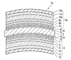
- FIG. 2 is a side sectional view schematically showing a second embodiment of the optical component of the present invention.
- reference numeral 1a is an optical component for a spectacle lens.
- This optical component 1a includes an inorganic multilayer film 3a disposed on the surface of the plastic substrate 2 in addition to the structure of the optical component 1 of the first embodiment having the inorganic multilayer film 3 on the back surface. . That is, in the optical component 1a of this embodiment, the inorganic multilayer film 3 is disposed on the back surface of the plastic substrate 2, and the inorganic multilayer film 3a is disposed on the surface.
- the functional thin film 4 is disposed between the surface of the plastic substrate 2 and the inorganic multilayer film 3a, as in the case of the back surface structure of the present embodiment. Also in this embodiment, the functional thin film 4 includes a primer layer 5 and a hard coat layer 6. In the present embodiment, as in the case of the back surface structure, a water / oil repellent film 12 is further provided on the inorganic multilayer film 3.
- the inorganic multilayer film 3a has a multilayer structure in which a plurality of high-refractive index inorganic materials and low-refractive index inorganic materials are alternately stacked on the plastic substrate 2 described above.
- the inorganic multilayer film 3a It has the same configuration. That is, the inorganic multilayer film 3a in the illustrated example has a five-layer structure in which five layers of high refractive index inorganic material and low refractive index inorganic material are alternately laminated on the plastic substrate 2 as described above.
- the inorganic multilayer film 3a, and the first layer 7a, the second layer 8a, the third layer 9a, the fourth layer 10a, and the fifth layer 11a constituting the inorganic multilayer film 3a are the back side inorganic multilayer film 3 and the inorganic multilayer film, respectively. Since it has the same configuration as the first layer 7, the second layer 8, the third layer 9, the fourth layer 10 and the fifth layer 11 constituting the film 3, the description thereof will be omitted. They may be the same or different as long as the limiting conditions of the present invention are satisfied.
- the manufacturing method of the present embodiment includes a step of forming the functional thin film 4 (primer layer 5 and hard coat layer 6) on the plastic substrate 2 by a method similar to the conventional method, and a step of heating the plastic substrate 2. After the plastic substrate 2 is adjusted to a predetermined temperature (for example, 70 ° C.) by heating, the step of forming the inorganic multilayer film 3 on the plastic substrate 2 and the formation of the water / oil repellent film 12 on the inorganic multilayer film 3 And a step of performing.
- a predetermined temperature for example, 70 ° C.
- the step of forming the inorganic multilayer film 3 is a process of alternately laminating a plurality of high refractive index inorganic materials and low refractive index inorganic materials to form a multilayer structure film.
- a low-refractive-index layer composed of the second layer 8 a high-refractive-index layer composed of a high-refractive-index inorganic material of the second layer 8, a low-refractive-index layer of the third layer 9, and a fourth layer 10
- the thick film of the high refractive index layer and the low refractive index layer of the fifth layer 11 are sequentially formed thereon.
- a vacuum deposition method is preferably used for forming each of the first to fifth layers.
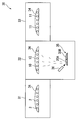
- FIG. 3 is a view showing an example of a vapor deposition apparatus 30 for forming the layers 7 to 11 of the inorganic multilayer film 3.
- the vapor deposition apparatus 30 includes a first film formation chamber 31, a second film formation chamber 32, and a third film formation chamber 33.
- Each of the first film forming chamber 31, the second film forming chamber 32, and the third film forming chamber 33 is configured so that the inside of each of the first film forming chamber 31, the second film forming chamber 32, and the third film forming chamber 33 is maintained in that state.
- the vapor deposition apparatus 30 can adjust the internal temperature of each of the first film forming chamber 31, the second film forming chamber 32, and the third film forming chamber 33 by temperature control means (not shown).
- the vapor deposition apparatus 30 includes a holding member 34 in each internal space of the first film formation chamber 31, the second film formation chamber 32, and the third film formation chamber 33.
- the holding member 34 has a curved upper surface (holding surface) and is configured to be rotatable, and holds a plurality of plastic substrates 2 on the upper surface.
- the vapor deposition source 35 of the vapor deposition apparatus 30 is disposed in a space inside the second film formation chamber 32.
- the vapor deposition source 35 includes a first vapor deposition source 35A and a second vapor deposition source 35B.
- a light source device 36 capable of irradiating the vapor deposition source 35 with a beam is disposed in the second film forming chamber 32.
- the light source device 36 can irradiate the vapor deposition source 35 with electrons and knock out the constituent particles of the vapor deposition source 35.
- the light source device 36 irradiates the second vapor deposition source 35 ⁇ / b> B with a beam to release SiO 2 vapor from the second vapor deposition source 35 ⁇ / b> B and supply the vapor onto the plastic substrate 2 held by the holding member 34. Evaporate. Thereby, the 1st layer 7, the 3rd layer 9, and the 5th layer 11 which are the low refractive index layers of the inorganic multilayer film 3 can be formed.
- the light source device 36 irradiates the first vapor deposition source 35 ⁇ / b > A with a beam, thereby releasing the vapor of ZrO 2 from the first vapor deposition source 35 ⁇ / b> A and supplying the vapor onto the plastic substrate 2 held by the holding member 34. And evaporate. Thereby, the second layer 8 and the fourth layer 10 which are high refractive index layers of the inorganic multilayer film 3 can be formed.
- the high refractive index inorganic material is formed on the plastic substrate 2 held by the holding member 34.
- layers made of a low refractive index inorganic material can be alternately formed and laminated.
- the average value of the reflectance in the wavelength range of 280 to 380 nm is 15% or less
- the fourth layer 10 as the high refractive index layer has an optical film thickness of 0.400 to 0.700 ⁇ . It is formed to be a thick film.
- the step of forming the inorganic multilayer film 3 includes the step of forming a film while performing ion beam assist on at least one of the layers constituting the inorganic multilayer film 3. May be included.
- the optical component manufacturing method of this embodiment includes such a step, so that a conductive film such as ITO or metal is disposed between the high refractive index inorganic material and the low refractive index inorganic material constituting the inorganic multilayer film. Established.
- FIG. 4 is a diagram showing an example of a film forming apparatus 30a for performing ion beam assist.
- the film forming apparatus 30a has a configuration in which an ion gun 37 is provided in the second film forming chamber of the film forming apparatus 30 shown in FIG.
- a conductor film such as ITO or metal is disposed between the fourth layer 10 which is a high refractive index layer and the fifth layer 11 which is a low refractive index layer constituting the inorganic multilayer film 3.
- film formation is performed while performing ion beam assist.
- at least one of the layers constituting the inorganic multilayer film 3 in the film forming chamber 32 may be formed while performing ion beam assist, and the target to be subjected to ion beam assist is not limited to the conductor film.
- the second film forming chamber of the film forming apparatus 30a includes a holding member 34 that holds the base material on which the fourth layer 10 is formed on the plastic base material 2, a vapor deposition source 35a, and a vapor deposition source.
- An ion gun 37 and a light source device 36 which are arranged apart from 35a are mainly configured. Further, the inside of the film forming apparatus 30a is depressurized to almost vacuum, so that the periphery of the plastic substrate 2 can be maintained in a vacuum atmosphere.
- an atmospheric gas supply source such as a gas cylinder is connected to the film forming apparatus 30a, and the inside of the vacuum vessel is in a low pressure state such as a vacuum, and an oxygen gas, argon gas, or other inert gas atmosphere, or in addition, an inert gas atmosphere containing oxygen can be formed.
- the vapor deposition source 35a includes, for example, ITO.
- ITO Indium Tin Oxide
- the light source device 36 irradiates the vapor deposition source 35 a with a beam, the gasified ITO is emitted from the vapor deposition source 35 a and supplied to the plastic substrate 2 held by the holding member 34. Thereby, a conductor film made of ITO can be formed on the fourth layer 10.
- the ion gun 37 is configured such that a gas to be ionized is introduced into the second film forming chamber 32 and a lead electrode is provided on the front surface.
- the light source device 36 has the same configuration as the ion gun 37, and can irradiate the vapor deposition source 35a with electrons to knock out the constituent particles of the vapor deposition source 35a.
- the constituent particles of the vapor deposition source 35a can be knocked out by applying a voltage to the vapor deposition source 35a with a high frequency coil or the like.
- the light source device 36 may be omitted.
- an ITO conductive film is formed on the fourth layer 10 of the high refractive index layer on the plastic substrate 2 using the film forming apparatus 30a having the above-described configuration.
- an ITO vapor deposition source 35 a is used, and ions irradiated from the ion gun 37 can be irradiated onto the upper surface of the holding member 34.
- the inside of the film forming chamber 32 containing the plastic substrate 2 is evacuated to make a reduced pressure atmosphere. Then, the ion gun 37 and the light source device 36 are operated.
- the constituent particles of the vapor deposition source 35a are knocked out and fly onto the fourth layer 10. Then, the constituent particles knocked out from the vapor deposition source 35 a are deposited on the fourth layer 10, and at the same time, argon ions are irradiated from the ion gun 37.
- the ion beam assist is preferably performed using at least one gas selected from an inert gas, an oxygen gas, and a mixed gas of an inert gas and an oxygen gas.
- the inert gas is preferably argon.
- the water / oil repellent film 12 is formed thereon to form the optical component 1.
- a wet method such as a dipping method, a spin coat method and a spray method, or a dry method such as a vacuum deposition method.
- the dipping method is common and is often used.
- the inorganic multilayer film 3 is formed in a solution obtained by dissolving a fluorine-substituted alkyl group-containing organosilicon compound in an organic solvent, the optical component is immersed, pulled up under certain conditions, and dried to form a film.
- the organic solvent perfluorohexane, perfluoro-4-methoxybutane, perfluoro-4-ethoxybutane, metaxylene hexafluoride, or the like is used.
- the dilution concentration with an organic solvent is preferably 0.01 to 0.5% by weight, more preferably 0.03 to 0.1% by weight. If the concentration is too low, the water / oil repellent layer 12 having a sufficient film thickness cannot be obtained, and if the concentration is too high, uneven coating tends to occur and the material cost increases. Of the dry methods, vacuum deposition is often used. This method is a method of forming the water- and oil-repellent film 12 by heating and evaporating the fluorine-substituted alkyl group-containing organosilicon compound in a vacuum chamber.
- the average value of the reflectance of the inorganic multilayer film 3 in the wavelength range of 280 to 380 nm is 20% or less, and the fourth layer 10 of the high refractive index layer is used. Since the optical film thickness is set to 0.400 to 0.700 ⁇ as the optical film thickness, as described above, both the reflection characteristics in the ultraviolet region and the visibility in the visible region should be ensured. Can do. Moreover, in the manufacturing method of an optical component, such a well-balanced and excellent optical component can be reliably provided.
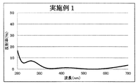
- Example 1 The lens is set in a rotating dome provided in the vacuum chamber, the temperature in the vacuum chamber is heated to 70 degrees, the pressure is exhausted until the pressure reaches 1.0 ⁇ 10 ⁇ 3 Pa, an acceleration voltage of 500 V, an acceleration current After performing Ar ion beam cleaning for 60 seconds under the condition of 100 mA, the first layer of SiO 2 (refractive index: 1.47) with an optical film thickness of 0.080 ⁇ and the second layer of ZrO 2 is sequentially formed from the plastic substrate side.
- Refractive index 2.00 is optical film thickness 0.080 ⁇
- third layer SiO 2 (refractive index 1.47) is optical film thickness 0.050 ⁇
- fourth layer ZrO 2 (refractive index 2.00).
- Example 2 The lens is set in a rotating dome provided in the vacuum chamber, the temperature in the vacuum chamber is heated to 70 degrees, the pressure is exhausted until the pressure reaches 1.0 ⁇ 10 ⁇ 3 Pa, an acceleration voltage of 500 V, an acceleration current After performing Ar ion beam cleaning for 60 seconds under the condition of 100 mA, the first layer of SiO 2 (refractive index: 1.47) with an optical film thickness of 0.080 ⁇ and the second layer of ZrO 2 is sequentially formed from the plastic substrate side.
- Refractive index 2.00 is optical film thickness 0.080 ⁇
- third layer SiO 2 (refractive index 1.47) is optical film thickness 0.060 ⁇
- fourth layer ZrO 2 (refractive index 2.00).
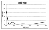
- the reflection spectral characteristics of the multilayer film of Example 2 thus obtained are shown in FIG. 6, and the configuration and film characteristics of the multilayer film of Example 2 are shown in Table 1.
- the multilayer film of Example 2 has a reflectance in the vicinity of 280 nm and 780 nm as a result of the ITO film provided between the fourth layer of ZrO 2 and the sixth layer of SiO 2.
- the reflection spectral characteristic balanced in both the visible region and the ultraviolet region is shown.
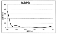
- Example 3 The lens is set in a rotating dome provided in the vacuum chamber, the temperature in the vacuum chamber is heated to 70 degrees, the pressure is exhausted until the pressure reaches 1.0 ⁇ 10 ⁇ 3 Pa, an acceleration voltage of 500 V, an acceleration current After Ar ion beam cleaning was performed for 60 seconds under the condition of 100 mA, the ZrO 2 (refractive index of 2.00) of the first layer was sequentially formed from the plastic substrate side with an optical film thickness of 0.050 ⁇ and the SiO 2 of the second layer. (Refractive index 1.47) is the optical film thickness 0.050 ⁇ , the third layer ZrO 2 (refractive index 2.00) is the optical film thickness 0.040 ⁇ , and the fourth layer SiO 2 (refractive index 1.47).
- Example 4 The lens is set in a rotating dome provided in the vacuum chamber, the temperature in the vacuum chamber is heated to 70 degrees, the pressure is exhausted until the pressure reaches 1.0 ⁇ 10 ⁇ 3 Pa, an acceleration voltage of 500 V, an acceleration current After performing Ar ion beam cleaning for 60 seconds under the condition of 100 mA, the first layer of SiO 2 (refractive index: 1.47) with an optical film thickness of 0.150 ⁇ and the second layer of ZrO 2 is sequentially formed from the plastic substrate side.
- Refractive index 2.00 is optical film thickness 0.060 ⁇
- third layer SiO 2 (refractive index 1.47) is optical film thickness 0.100 ⁇
- fourth layer ZrO 2 (refractive index 2.00).
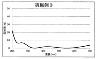
- the multilayer film of Example 4 With an optical film thickness of 0.440 ⁇ and a fifth layer of SiO 2 (refractive index of 1.47) with an optical film thickness of 0.270 ⁇ . Note that ⁇ is 500 nm as the design center wavelength.
- the reflection spectral characteristics of the multilayer film of Example 4 thus obtained are shown in FIG. 8, and the configuration and film characteristics of the multilayer film of Example 4 are shown in Table 1. As is clear from FIG. 8, the multilayer film of Example 4 has a little higher reflectance near 280 nm and 780 nm, but has a reflection spectral characteristic similar to that shown in FIG. You can see that
- Example 5 The lens is set in a rotating dome provided in the vacuum chamber, the temperature in the vacuum chamber is heated to 70 degrees, the pressure is exhausted until the pressure reaches 1.0 ⁇ 10 ⁇ 3 Pa, an acceleration voltage of 500 V, an acceleration current After Ar ion beam cleaning was performed for 60 seconds under the condition of 100 mA, the ZrO 2 (refractive index of 2.00) of the first layer was sequentially formed from the plastic substrate side with an optical film thickness of 0.050 ⁇ and the SiO 2 of the second layer. (Refractive index 1.47) is the optical film thickness 0.050 ⁇ , the third layer ZrO 2 (refractive index 2.00) is the optical film thickness 0.090 ⁇ , and the fourth layer SiO 2 (refractive index 1.47).
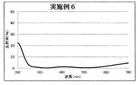
- Example 6> The lens is set in a rotating dome provided in the vacuum chamber, the temperature in the vacuum chamber is heated to 70 degrees, the pressure is exhausted until the pressure reaches 1.0 ⁇ 10 ⁇ 3 Pa, an acceleration voltage of 500 V, an acceleration current After Ar ion beam cleaning was performed for 60 seconds under the condition of 100 mA, the ZrO 2 (refractive index of 2.00) of the first layer was sequentially formed from the plastic substrate side with an optical film thickness of 0.040 ⁇ and the second layer of SiO 2. (Refractive index 1.47) is the optical film thickness 0.070 ⁇ , the third layer ZrO 2 (refractive index 2.00) is the optical film thickness 0.060 ⁇ , and the fourth layer SiO 2 (refractive index 1.47).
- the reflection spectral characteristics of the multilayer film of Example 6 thus obtained are shown in FIG. 10, and the configuration and film characteristics of the multilayer film of Example 6 are shown in Table 2. As is clear from FIG.
- the multilayer film of Example 6 has a slightly higher reflectance near 280 nm and does not have a peak (extreme value) in the ultraviolet region, but the average reflectance is sufficiently low, and the visible region is It can be seen that the reflection spectral characteristic similar to that shown in FIG.
- Example 7 The lens is set in a rotating dome provided in the vacuum chamber, the temperature in the vacuum chamber is heated to 70 degrees, the pressure is exhausted until the pressure reaches 1.0 ⁇ 10 ⁇ 3 Pa, an acceleration voltage of 500 V, an acceleration current
- the first layer of TiO 2 (refractive index of 2.49) is sequentially formed from the plastic substrate side with an optical film thickness of 0.050 ⁇ and a second layer of MgF 2 ( Refractive index 1.38) is optical thickness 0.050 ⁇
- third layer TiO 2 (refractive index 2.49) is optical thickness 0.410 ⁇
- fourth layer MgF 2 (refractive index 1.38) is optical.
- the optical film thickness is 0.020 ⁇
- the fifth layer TiO 2 (refractive index 2.49) is the optical film thickness 0.080 ⁇
- the sixth layer SiO 2 (refractive index 1.47) is the optical film thickness 0.220 ⁇ .
- ⁇ is 500 nm as the design center wavelength.
- the reflection spectral characteristics of the multilayer film of Example 7 thus obtained are shown in FIG. 11, and the configuration and film characteristics of the multilayer film of Example 7 are shown in Table 2.
- the multilayer film of Example 7 uses TiO 2 for the high refractive index layer and MgF 2 and SiO 2 for the low refractive index layer. It can be seen that the reflection spectral characteristic similar to that shown in FIG.
- the SiO 2 (refractive index of 1.47) of the first layer is sequentially formed from the plastic substrate side with an optical film thickness of 0.110 ⁇
- the second layer of ZrO 2 (refractive index 2.00) has an optical thickness of 0.150 ⁇
- the third layer of SiO 2 (refractive index 1.47) has an optical thickness of 0.080 ⁇
- the fourth layer of ZrO 2 A (refractive index of 2.00) was laminated with an optical film thickness of 0.230 ⁇
- a fifth layer of SiO 2 (refractive index of 1.47) was laminated with an optical film thickness of 0.280 ⁇ .
- ⁇ is 500 nm as the design center wavelength.
- the reflection spectral characteristics of the multilayer film of Comparative Example 1 thus obtained are shown in FIG. 12, and the configuration and film characteristics of the multilayer film of Comparative Example 1 are shown in Table 3.
- the multilayer film of Comparative Example 1 is a general antireflection film used for spectacle lenses, and has a large reflectance peak in the ultraviolet region, and is shown in FIG. It can be seen that the reflection spectral characteristic is completely different from the reflection spectral characteristic.
- the SiO 2 (refractive index: 1.47) of the first layer is sequentially formed from the plastic substrate side with an optical film thickness of 0.150 ⁇
- the second layer ZrO 2 (refractive index 2.00) has an optical film thickness of 0.150 ⁇
- the third layer SiO 2 (refractive index 1.47) has an optical film thickness of 0.060 ⁇
- a (refractive index of 2.00) was laminated with an optical film thickness of 0.350 ⁇
- a fifth layer of SiO 2 (refractive index of 1.47) was laminated with an optical film thickness of 0.270 ⁇ .
- ⁇ is 500 nm as the design center wavelength.
- the reflection spectral characteristics of the multilayer film of Comparative Example 2 thus obtained are shown in FIG. 13, and the configuration and film characteristics of the multilayer film of Comparative Example 2 are shown in Table 3.
- the multilayer film of Comparative Example 2 has a large reflectance peak in the ultraviolet region because the thickness of the thick film of the high refractive index layer is a little thinner than specified. It can be seen that the reflection spectral characteristic completely different from the reflection spectral characteristic shown in FIG.
- ⁇ Comparative Example 3> The lens is set in a rotating dome provided in the vacuum chamber, the temperature in the vacuum chamber is heated to 70 degrees, the pressure is exhausted until the pressure reaches 1.0 ⁇ 10 ⁇ 3 Pa, an acceleration voltage of 500 V, an acceleration current After Ar ion beam cleaning was performed for 60 seconds under the condition of 100 mA, the ZrO 2 (refractive index of 2.00) of the first layer was sequentially formed from the plastic substrate side with an optical film thickness of 0.040 ⁇ and the second layer of SiO 2. (Refractive index 1.47) is the optical film thickness 0.140 ⁇ , the third layer ZrO 2 (refractive index 2.00) is the optical film thickness 0.050 ⁇ , and the fourth layer SiO 2 (refractive index 1.47).
- the multilayer film of Comparative Example 3 has a large reflectance peak in the ultraviolet region because the thickness of the thick film of the high refractive index layer is larger than specified, and FIG. It can be seen that the reflection spectral characteristic completely different from the reflection spectral characteristic shown in FIG.
- Comparative Example 2 is a design in which the film thickness of the high refractive index layer is smaller (thin) than that of the present invention
- Comparative Example 3 is a design in which the film thickness of the high refractive index layer is larger (thicker) than that of the present invention.
- Comparative Example 2 the average reflectance of ultraviolet rays at an incident angle of 0 degrees and 35 degrees is 15% or more, and in Comparative Example 3, the average reflectance of ultraviolet rays at an incident angle of 0 degrees is 15% or more. It can be seen that the hue angle of light is 293 degrees, which greatly deviates from the hue angle of reflected light in a general spectacle lens.
- Example 4 is a design in which the ratio of the highly bent layer to the total film thickness of the multilayer film is small.
- the characteristics in the visible region and the average reflectance in the ultraviolet region are within the specified range, but the luminous reflectance and the average reflectance in the ultraviolet region are slightly inferior to those in Examples 1 to 3. I understand.
- Example 5 is a design in which a thick film of a high refractive index layer is installed in the vicinity of the middle of the multilayer film. Also in this case, the luminous reflectance is larger than in Examples 1 to 3. From the above results, the effect of the present invention is clear.
- the multilayer film disposed on the back surface of the lens is within the specified range of the present invention, the surface reflection in the ultraviolet region is not impaired and the characteristics of the existing antireflection film are not impaired. It is apparent that an optical component capable of suppressing the incidence on the eyeball due to the reflection of the ultraviolet light incident from the rear and the manufacturing method thereof can be provided depending on the characteristics.
- the anti-glare effect, good visibility, and low surface reflection characteristics in the ultraviolet region can suppress incidence on the eyeball due to reflection of ultraviolet light incident from the rear. It is clear that an optical component and a manufacturing method thereof can be provided.
Abstract
La présente invention vise à proposer un élément optique ayant une bonne visibilité et qui est également efficace pour empêcher une maladie oculaire, et la présente invention porte sur un élément optique dans lequel un film multicouche est disposé sur les deux surfaces d'une lentille plastique, un film multicouche disposé sur une surface arrière ayant une réflectance moyenne de 15 % au maximum dans une région de longueur d'onde de 280 nm à 380 nm lorsque l'angle d'incidence est de 0° à 45°, le film multicouche disposé sur la surface arrière comprenant au moins trois couches d'indice de réfraction élevé et couches d'indice de réfraction faible superposées les unes sur les autres, et au moins une couche d'indice de réfraction élevé dans le film multicouche disposé sur la surface arrière étant un film épais ayant une épaisseur de film optique de 0,4000-0,700 λ.
Applications Claiming Priority (2)
| Application Number | Priority Date | Filing Date | Title |
|---|---|---|---|
| JP2013132456A JP2015007695A (ja) | 2013-06-25 | 2013-06-25 | 光学部品 |
| JP2013-132456 | 2013-06-25 |
Publications (1)
| Publication Number | Publication Date |
|---|---|
| WO2014208412A1 true WO2014208412A1 (fr) | 2014-12-31 |
Family
ID=52141752
Family Applications (1)
| Application Number | Title | Priority Date | Filing Date |
|---|---|---|---|
| PCT/JP2014/066122 WO2014208412A1 (fr) | 2013-06-25 | 2014-06-18 | Élément optique |
Country Status (2)
| Country | Link |
|---|---|
| JP (1) | JP2015007695A (fr) |
| WO (1) | WO2014208412A1 (fr) |
Cited By (4)
| Publication number | Priority date | Publication date | Assignee | Title |
|---|---|---|---|---|
| WO2016088763A1 (fr) * | 2014-12-01 | 2016-06-09 | ホヤ レンズ タイランド リミテッド | Verre de lunettes et lunettes |
| WO2016181932A1 (fr) * | 2015-05-11 | 2016-11-17 | 株式会社ニコン・エシロール | Verre de lunettes |
| WO2020004414A1 (fr) * | 2018-06-29 | 2020-01-02 | ホヤ レンズ タイランド リミテッド | Verre de lunettes et lunettes |
| CN113039461A (zh) * | 2018-11-19 | 2021-06-25 | 依视路国际公司 | 具有干涉涂层和用于改善耐磨性的多层系统的光学镜片 |
Families Citing this family (6)
| Publication number | Priority date | Publication date | Assignee | Title |
|---|---|---|---|---|
| WO2017077357A1 (fr) * | 2015-11-06 | 2017-05-11 | Essilor International (Compagnie Générale d'Optique) | Article optique protégeant de la lumière bleue |
| JP2018536894A (ja) * | 2015-11-06 | 2018-12-13 | エシロール アンテルナショナルEssilor International | 青色光及びuv光から保護する光学物品 |
| JP7129781B2 (ja) * | 2018-01-25 | 2022-09-02 | 株式会社乾レンズ | 眼鏡用レンズ及び眼鏡 |
| JP2023182010A (ja) * | 2019-09-30 | 2023-12-26 | ホヤ レンズ タイランド リミテッド | 眼鏡レンズ |
| JP2023182008A (ja) * | 2019-09-30 | 2023-12-26 | ホヤ レンズ タイランド リミテッド | 眼鏡レンズ |
| WO2021240805A1 (fr) * | 2020-05-29 | 2021-12-02 | 株式会社乾レンズ | Verre de lunettes et lunettes |
Citations (4)
| Publication number | Priority date | Publication date | Assignee | Title |
|---|---|---|---|---|
| JP2001131420A (ja) * | 1999-11-05 | 2001-05-15 | Asahi Optical:Kk | プラスチック基材 |
| JP2006284778A (ja) * | 2005-03-31 | 2006-10-19 | Hoya Corp | スプラッシュ抑制方法およびプラスチックレンズの製造方法 |
| WO2010125667A1 (fr) * | 2009-04-30 | 2010-11-04 | 山本光学株式会社 | Verre de lunettes |
| WO2012076714A1 (fr) * | 2010-12-10 | 2012-06-14 | Essilor International (Compagnie Generale D'optique) | Article optique comprenant un revêtement antiréfléchissant et présentant une faible réflexion dans le domaine de l'ultraviolet et dans le domaine visible |
Family Cites Families (2)
| Publication number | Priority date | Publication date | Assignee | Title |
|---|---|---|---|---|
| JP2005215038A (ja) * | 2004-01-27 | 2005-08-11 | Seiko Epson Corp | 眼鏡レンズ |
| JP5007843B2 (ja) * | 2009-09-24 | 2012-08-22 | 信越化学工業株式会社 | フォトマスクブランク及びフォトマスク |
-
2013
- 2013-06-25 JP JP2013132456A patent/JP2015007695A/ja active Pending
-
2014
- 2014-06-18 WO PCT/JP2014/066122 patent/WO2014208412A1/fr active Application Filing
Patent Citations (4)
| Publication number | Priority date | Publication date | Assignee | Title |
|---|---|---|---|---|
| JP2001131420A (ja) * | 1999-11-05 | 2001-05-15 | Asahi Optical:Kk | プラスチック基材 |
| JP2006284778A (ja) * | 2005-03-31 | 2006-10-19 | Hoya Corp | スプラッシュ抑制方法およびプラスチックレンズの製造方法 |
| WO2010125667A1 (fr) * | 2009-04-30 | 2010-11-04 | 山本光学株式会社 | Verre de lunettes |
| WO2012076714A1 (fr) * | 2010-12-10 | 2012-06-14 | Essilor International (Compagnie Generale D'optique) | Article optique comprenant un revêtement antiréfléchissant et présentant une faible réflexion dans le domaine de l'ultraviolet et dans le domaine visible |
Cited By (16)
| Publication number | Priority date | Publication date | Assignee | Title |
|---|---|---|---|---|
| US10690944B2 (en) | 2014-12-01 | 2020-06-23 | Hoya Lens Thailand Ltd. | Spectacle lens that reflects blue light, and spectacles equipped with the spectacle lens |
| WO2016088763A1 (fr) * | 2014-12-01 | 2016-06-09 | ホヤ レンズ タイランド リミテッド | Verre de lunettes et lunettes |
| WO2016181932A1 (fr) * | 2015-05-11 | 2016-11-17 | 株式会社ニコン・エシロール | Verre de lunettes |
| KR20170135930A (ko) * | 2015-05-11 | 2017-12-08 | 가부시키가이샤 니콘. 에시로루 | 안경 렌즈 |
| CN107533243A (zh) * | 2015-05-11 | 2018-01-02 | 株式会社尼康依视路 | 眼镜透镜 |
| JPWO2016181932A1 (ja) * | 2015-05-11 | 2018-02-22 | 株式会社ニコン・エシロール | 眼鏡レンズ |
| EP3296800A4 (fr) * | 2015-05-11 | 2018-12-19 | Nikon-Essilor Co., Ltd. | Verre de lunettes |
| KR101986931B1 (ko) * | 2015-05-11 | 2019-06-07 | 가부시키가이샤 니콘. 에시로루 | 안경 렌즈 |
| US10908436B2 (en) | 2015-05-11 | 2021-02-02 | Nikon-Essilor Co., Ltd. | Spectacle lens |
| CN107533243B (zh) * | 2015-05-11 | 2020-02-28 | 株式会社尼康依视路 | 眼镜透镜 |
| JP2020003706A (ja) * | 2018-06-29 | 2020-01-09 | ホヤ レンズ タイランド リミテッドHOYA Lens Thailand Ltd | 眼鏡レンズおよび眼鏡 |
| WO2020004414A1 (fr) * | 2018-06-29 | 2020-01-02 | ホヤ レンズ タイランド リミテッド | Verre de lunettes et lunettes |
| JP7303613B2 (ja) | 2018-06-29 | 2023-07-05 | ホヤ レンズ タイランド リミテッド | 眼鏡レンズおよび眼鏡 |
| US11860452B2 (en) | 2018-06-29 | 2024-01-02 | Hoya Lens Thailand Ltd. | Spectacle lens and spectacles |
| CN113039461A (zh) * | 2018-11-19 | 2021-06-25 | 依视路国际公司 | 具有干涉涂层和用于改善耐磨性的多层系统的光学镜片 |
| CN113039461B (zh) * | 2018-11-19 | 2023-07-14 | 依视路国际公司 | 具有干涉涂层和用于改善耐磨性的多层系统的光学镜片 |
Also Published As
| Publication number | Publication date |
|---|---|
| JP2015007695A (ja) | 2015-01-15 |
Similar Documents
| Publication | Publication Date | Title |
|---|---|---|
| JP6073355B2 (ja) | 眼鏡レンズ、及び眼鏡レンズの製造方法 | |
| JP5966011B2 (ja) | 眼鏡レンズおよびその製造方法 | |
| JP5795675B2 (ja) | 眼鏡レンズ用光学部品、眼鏡レンズ用光学部品の製造方法 | |
| WO2014208412A1 (fr) | Élément optique | |
| JP6581653B2 (ja) | 眼鏡レンズ | |
| KR101477940B1 (ko) | 광학 부품 및 그의 제조방법 | |
| JP5173076B2 (ja) | 光学部品およびその製造方法 |
Legal Events
| Date | Code | Title | Description |
|---|---|---|---|
| 121 | Ep: the epo has been informed by wipo that ep was designated in this application |
Ref document number: 14817873 Country of ref document: EP Kind code of ref document: A1 |
|
| NENP | Non-entry into the national phase |
Ref country code: DE |
|
| 122 | Ep: pct application non-entry in european phase |
Ref document number: 14817873 Country of ref document: EP Kind code of ref document: A1 |