WO2014208412A1 - Optical component - Google Patents
Optical component Download PDFInfo
- Publication number
- WO2014208412A1 WO2014208412A1 PCT/JP2014/066122 JP2014066122W WO2014208412A1 WO 2014208412 A1 WO2014208412 A1 WO 2014208412A1 JP 2014066122 W JP2014066122 W JP 2014066122W WO 2014208412 A1 WO2014208412 A1 WO 2014208412A1
- Authority
- WO
- WIPO (PCT)
- Prior art keywords
- refractive index
- layer
- multilayer film
- film
- back surface
- Prior art date
Links
Images


Classifications
-
- G—PHYSICS
- G02—OPTICS
- G02B—OPTICAL ELEMENTS, SYSTEMS OR APPARATUS
- G02B1/00—Optical elements characterised by the material of which they are made; Optical coatings for optical elements
- G02B1/10—Optical coatings produced by application to, or surface treatment of, optical elements
- G02B1/11—Anti-reflection coatings
- G02B1/113—Anti-reflection coatings using inorganic layer materials only
- G02B1/115—Multilayers
-
- G—PHYSICS
- G02—OPTICS
- G02B—OPTICAL ELEMENTS, SYSTEMS OR APPARATUS
- G02B5/00—Optical elements other than lenses
- G02B5/20—Filters
- G02B5/28—Interference filters
- G02B5/283—Interference filters designed for the ultraviolet
-
- G—PHYSICS
- G02—OPTICS
- G02C—SPECTACLES; SUNGLASSES OR GOGGLES INSOFAR AS THEY HAVE THE SAME FEATURES AS SPECTACLES; CONTACT LENSES
- G02C7/00—Optical parts
- G02C7/02—Lenses; Lens systems ; Methods of designing lenses
-
- G—PHYSICS
- G02—OPTICS
- G02C—SPECTACLES; SUNGLASSES OR GOGGLES INSOFAR AS THEY HAVE THE SAME FEATURES AS SPECTACLES; CONTACT LENSES
- G02C2202/00—Generic optical aspects applicable to one or more of the subgroups of G02C7/00
- G02C2202/16—Laminated or compound lenses
Definitions
- the present invention relates to an optical component such as a spectacle lens.
- plastic lenses are frequently used for spectacle lenses because of their advantages of being lightweight, excellent in impact resistance and easy to dye.
- plastic lenses used for spectacle lenses are usually provided with antireflection films on both sides.
- antireflection films for spectacle lenses generally have low reflection characteristics (broadband low reflection characteristics) over the entire visible region of 380 nm to 780 nm.
- ultraviolet rays of 280 nm to 380 nm are known to cause damage to the retina due to exposure to the eyeball. It is considered desirable to cut off light in the ultraviolet region because long-term exposure to ultraviolet rays outdoors causes keratitis, cataracts, and the like.
- dyed lenses such as sunglasses are known.
- some spectacle lenses contain a UV absorber in the lens body and some are provided with UV cut coating. . In such sunglasses and conventional spectacle lenses, it is possible to reduce or block ultraviolet rays incident from the front surface (front surface; the surface opposite to the eyeball) of the spectacle lens.
- Patent Document 1 discloses a spectacle lens in which an inorganic film having a surface reflectance smaller than that of the lens base material itself is formed on the back surface of the spectacle lens with respect to all rays in the wavelength region of 280 to 315 nm and 420 to 680 nm. It is disclosed.
- the spectacle lens disclosed in Patent Document 1 it is possible to reliably prevent ultraviolet rays from the rear in the line of sight, particularly far ultraviolet rays, from being reflected from the back surface of the lens, thereby reducing the amount of ultraviolet rays entering the eye. It is said.
- Patent Document 2 discloses a multilayer structure comprising a laminated body of at least one high refractive index layer having a refractive index of 1.6 or more and at least one low refractive index layer having a refractive index of 1.5 or less on the back surface of the spectacle lens.
- An eyeglass lens having an antireflection film which has an average reflectance Rm in the visible range of 1.15% or less, a luminous reflectance Rv of 1% or less, and incident angles of 30 ° and 45 °,
- the weighted average reflectance Ruv (ISO 13666: 1998 Standard) in the wavelength region of 380 nm is 5% or less
- the multilayer film is 3 to 7 layers
- the outer layer of the multilayer film is An eyeglass lens that is a silica-based film is disclosed.
- ultraviolet and antireflection films having good antireflection performance in the visible region and the ultraviolet region are formed on the back surface of the lens.
- the present invention has been made in view of the above circumstances, and an object of the present invention is to provide an optical component that is effective in preventing eye diseases and has good visibility. That is, the object of the present invention is to eliminate the above-mentioned problems of the prior art, suppress degradation of performance such as heat resistance, crack resistance and durability, and prevent reflection in the ultraviolet region without any deterioration in optical performance in the visible region. It is to provide an optical component with excellent performance.
- an optical component of the present invention is an optical component including a multilayer film on at least the back surface of a plastic lens, and the multilayer film disposed on the back surface of the plastic lens has an incident angle.
- the average reflectance in the wavelength region of 280 nm to 380 nm at 0 ° to 45 ° is 15% or less
- the multilayer film disposed on the back surface includes a high refractive index layer made of a high refractive index material and a low refractive index.
- the optical film thickness of the at least one high refractive index layer in the multilayer film disposed on the back surface is three or more layers with a low refractive index layer made of a refractive index material. It is a thick film having a thickness of 0.700 ⁇ .
- the ratio of the high refractive index layer to the total film thickness of the multilayer film disposed on the back surface is preferably greater than 45%.
- the multilayer film disposed on the back surface preferably has an average reflectance of 10% or less in a wavelength region of 280 nm to 380 nm when the incident angle is 0 degree to 45 degrees. Further, it is preferable that a luminous reflectance of reflected light of the multilayer film disposed on the back surface is 1.5% or less and a hue angle thereof is 120 to 220 degrees.
- the one high refractive index layer that is the thick film is a layer farthest from the base material of the plastic lens among the high refractive index layers in the multilayer film disposed on the back surface.
- a conductor film, a metal film, or a visible light absorbing film is provided between the high refractive index layer and the low refractive index layer constituting the multilayer film disposed on the back surface.
- the plastic lens preferably has a function of absorbing ultraviolet rays.
- the base material of the plastic lens may be colored.
- the transmittance of the colored plastic lens substrate is preferably 5 to 85%.
- the spectral characteristic curve representing the reflectance of the multilayer film disposed on the back surface with respect to the wavelength is a curve having one extreme value or a monotone having no extreme value.
- the spectral characteristic curve is a curve having the one extreme value
- the one extreme value is preferably a reflectance of 20% or less.
- the multilayer film may be disposed on the surface of the plastic lens in addition to the back surface of the plastic lens.
- the optical multilayer film configured as described above can obtain a sufficient ultraviolet ray cutting effect while maintaining good visibility without changing in the characteristics of the visible region as compared with the conventional spectacle lens.
- it since it is configured as described above, it suppresses deterioration of performance such as heat resistance, crack resistance and durability, and does not deteriorate optical performance in the visible region, and prevents reflection in the ultraviolet region.
- An optical component having excellent performance can be provided.
- it is possible to provide an optical component having reduced optical intensity in the eyeball, reduced glare, easy to see, and effective optical properties for fatigue and eye disease prevention. It becomes.
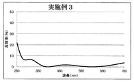
- 10 is a graph showing a spectral characteristic curve of a multilayer film on the back surface of the lens of Example 3.
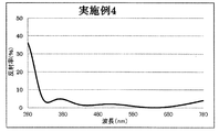
- 6 is a graph showing a spectral characteristic curve of a multilayer film on the back surface of the lens of Example 4.
- 6 is a graph showing a spectral characteristic curve of a multilayer film on the back surface of the lens of Example 5.
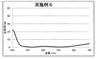
- 14 is a graph showing a spectral characteristic curve of a multilayer film on the back surface of the lens of Example 6.
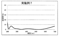
- 10 is a graph showing a spectral characteristic curve of a multilayer film on the back surface of the lens of Example 7.
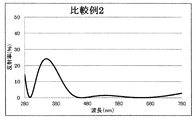
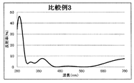
- 6 is a graph showing a spectral characteristic curve of a multilayer film on the back surface of the lens of Comparative Example 1; 6 is a graph showing a spectral characteristic curve of a multilayer film on the back surface of the lens of Comparative Example 2. 10 is a graph showing a spectral characteristic curve of a multilayer film on the back surface of the lens of Comparative Example 3.
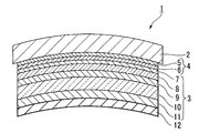
- FIG. 1 is a sectional side view which shows typically an example of the optical component which concerns on 1st Embodiment of this invention.
- An optical component 1 shown in FIG. 1 is an optical component for a spectacle lens, and includes a plastic substrate 2 and an inorganic multilayer film 3 disposed on the back surface of the plastic substrate 2.
- a functional thin film 4 is disposed between the back surface of the plastic substrate 2 and the inorganic multilayer film 3, and the functional thin film 4 includes a primer layer 5 and a hard coat layer. It consists of six.
- a water / oil repellent film 12 is further provided on the inorganic multilayer film 3. The water / oil repellent film 12 will be described later.
- arbitrary films corresponding to the inorganic multilayer film 3 and the functional thin film 4 are also formed on the surface of the plastic substrate 2, but illustration and description of such films are omitted.
- the plastic substrate 2 is, for example, a transparent plastic such as acrylic resin, thiourethane resin, methacrylic resin, allyl resin, episulfide resin, polycarbonate resin, polyurethane resin, polyester resin, polystyrene resin, episulfide. Resin, polyethersulfone resin poly-4-methylpentene-1 resin, diethylene glycol bisallyl carbonate resin (CR-39), polyvinyl chloride resin, halogen-containing copolymer, sulfur-containing copolymer, etc. is there.
- the refractive index (nd) of the plastic substrate 2 is selected from, for example, 1.50, 1.60, 1.67, and 1.74.
- the plastic substrate 2 When the refractive index of the plastic substrate 2 is 1.6 or more, it is preferable to use an allyl carbonate resin, an acrylate resin, a methacrylate resin, a thiourethane resin, or the like as the plastic substrate 2. .
- the plastic substrate 2 preferably has a function of absorbing ultraviolet rays. That is, it is preferable that the resin constituting the plastic substrate 2 contains an ultraviolet absorber.
- the functional thin film 4 disposed on the surface of the plastic substrate 2 may contain an ultraviolet absorber. In such a case, the plastic substrate 2 is impregnated with the ultraviolet absorbent component in the functional thin film 4.
- the plastic substrate 2 may not be transparent as long as it has translucency, and may be colored.
- the transmittance of the colored plastic substrate 2 is preferably 5 to 85%.
- the functional thin film 4 is disposed between the plastic substrate 2 and the inorganic multilayer film 3 as described above, and a primer layer 5 disposed in contact with the plastic substrate 2, and the primer layer 5 And a hard coat layer 6 disposed in contact with the inorganic multilayer film 3.
- the primer layer 5 is for improving the adhesion between the plastic substrate 2 and the hard coat layer 6 and functions as an adhesion layer. Moreover, it is also for absorbing the impact on the optical component 1 and functions as an impact absorbing layer.
- the primer layer 5 is mainly composed of a polyurethane-based resin, and in this embodiment, the polyurethane-based resin contains, for example, fine particles of an inorganic material.
- the primer layer 5 may contain at least one of acrylic resin, methacrylic resin, and organosilicon resin.
- the thickness (actual thickness) of the primer layer 5 is preferably about 0.5 ⁇ m or more and 1.0 ⁇ m or less.
- Such a primer layer 5 can be formed on the plastic substrate 2 with a predetermined thickness by immersing the plastic substrate 2 in a material solution for forming the primer layer 5 and then lifting and drying.
- a material for forming the primer layer 5 for example, a liquid obtained by dispersing or dissolving the above-described resin and the inorganic oxide fine particle sol in water or an alcohol solvent and mixing them can be used.
- the hard coat layer 6 has a function of protecting the plastic substrate 2 and suppressing damage to the plastic substrate 2, and functions as a scratch-resistant film.
- the hard coat layer 6 is made of, for example, an organosiloxane hard coat layer.
- the organosiloxane hard coat layer is obtained by dispersing inorganic oxide fine particles in an organosiloxane resin.
- the inorganic oxide for example, rutile type titanium oxide, oxides of silicon, tin, zirconium, and antimony are preferably used.
- the hard coat layer 6 may be an organic silicon-based resin containing colloidal silica as disclosed in, for example, Japanese Patent Publication No. 4-55615.
- the thickness (actual thickness) of the hard coat layer 6 is preferably about 2 ⁇ m to 4 ⁇ m.
- the hard coat layer 6 is formed on the primer layer 5 on the plastic substrate 2 by immersing the plastic substrate 2 on which the primer layer 5 is formed in the forming material solution of the hard coat layer 6 and then lifting and drying. It can be formed with a thickness of As the forming material liquid for the hard coat layer 6, for example, a liquid obtained by dispersing or dissolving the above-described resin to be the hard coat layer 6 and the inorganic oxide fine particle sol in water or an alcohol-based solvent can be used. .
- the interface between the functional thin film 4 and the plastic substrate 2 is sufficient if the refractive index and the refractive index of the plastic substrate 2 are substantially the same. Generation of interference fringes caused by reflection on the surface and a decrease in transmittance can be suppressed. Therefore, it is desirable to adjust the refractive index of the functional thin film 4 in accordance with the refractive index of the plastic substrate 2.
- the type (physical properties) of the resin that is the main component of the functional thin film 4 is selected, or the resin that is the main component This can be done by selecting the type (physical properties) of the fine particles to be added.
- the functional thin film 4 is formed including the primer layer 5 and the hard coat layer 6.
- the primer layer 5 and the hard coat layer 6 are formed. It may be omitted.
- a conductor film made of ITO (Indium Tin Oxide) a metal film such as Ni, Cr, or a visible light absorption layer
- the above-described primer layer 5 and hard coat layer 6 are used. In addition to this, it may be arranged.
- a conductive film such as ITO or a metal film such as Ni or Cr having a thickness of 20 nm or less between the high refractive index inorganic material and the low refractive index inorganic material constituting the inorganic multilayer film 3.
- a visible light absorption film or the like may be provided.
- the thickness of the conductor film, metal film or visible light may be 10 nm or less.
- the conductor film, the metal film, or the visible light absorption film is more electrically conductive than the oxide that is a high refractive index inorganic material used in the multilayer film of the present invention, and also absorbs visible light.
- the inorganic multilayer film 3 has a multilayer structure in which a plurality of high refractive index inorganic materials (high refractive index substances) and low refractive index inorganic materials (low refractive index substances) are alternately stacked on the plastic substrate 2 described above.
- the antireflection film has a multilayer structure in which a high refractive index layer made of a high refractive index material and a low refractive index layer made of a low refractive index material are stacked in three or more layers, and prevents reflection of incident light. It has the function as.
- the inorganic multilayer film 3 is designed so that the average reflectance in the wavelength region (ultraviolet region) of 280 nm to 380 nm when the incident angle is 0 degree to 45 degrees is 15% or less.
- the average reflectance in the ultraviolet region is preferably 10% or less, for example, the average reflectance in the ultraviolet region when the incident angle is 0 degrees is 4% or more, and the ultraviolet region when the incident angle is 45 degrees.
- An average reflectance of 2.5% or more is particularly preferable.
- the reason why the average reflectance in the ultraviolet region is limited to 15% or less is that when the average reflectance is set to 15% or less, the light in the ultraviolet region can be sufficiently cut, and when used as a spectacle lens, A filter function such as a sufficient antiglare effect can be obtained while maintaining good visibility, and ultraviolet rays incident on the eyeball can be reduced.
- the average reflectance in the ultraviolet region is set to more than 15%, the wearer of the spectacle lens enters from behind or obliquely from the side and is reflected by the back surface of the lens and reaches the eyeball.
- the average reflectance in the ultraviolet region is preferably as low as possible.
- the average reflectance is not particularly limited, and the balance with the reflectance in the wavelength region (visible region) of 380 to 780 nm (visible light cutting ability) is as follows: It is sufficient to set appropriately so as not to cause a decrease in the amount of transmitted light and a deterioration in visibility.
- the average reflectance in the ultraviolet region when the incident angle is 0 degree is 4% or more, and the average reflectance in the ultraviolet region when the incident angle is 45 degrees is particularly preferably 2.5% or more. If the average reflectance in the ultraviolet region is within such a range, it is easy to sufficiently reduce the reflection of ultraviolet rays without departing from the reflection property of a spectacle lens that is generally used in the visible region.
- an inorganic multilayer film is used as the multilayer film, but an organic multilayer film may be used as long as the effects of the present invention are not impaired.
- an inorganic multilayer film (not shown) is disposed on the front surface (front surface) in addition to the back surface (rear surface) of the plastic substrate 2.
- the average reflectance in the wavelength range of 280 to 380 nm of the inorganic multilayer film disposed on the surface of the plastic substrate 2 is in the wavelength range of 280 to 380 nm of the inorganic multilayer film 3 disposed on the back surface of the plastic substrate 2. It is preferable that it is larger than the average reflectance.
- the inorganic multilayer film 3 disposed on the back surface of the plastic substrate 2 has an average reflectance of 15% or less in the wavelength range of 280 to 380 nm, and the inorganic multilayer film disposed on the surface of the plastic substrate 2.
- the inorganic multilayer film 3 in the illustrated example has a five-layer structure in which five layers of a high refractive index inorganic material and a low refractive index inorganic material are alternately laminated on the plastic substrate 2 as described above.
- a first layer (low refractive index layer) 7 made of a low refractive index inorganic material provided on the side, and a second layer (high refractive index layer) 8 made of a high refractive index inorganic material provided on the first layer 7.
- the multilayer film 3 is not particularly limited as long as three or more layers of the high refractive index inorganic material and the low refractive index inorganic material are alternately laminated on the plastic base material 2.
- the multilayer film is preferably 10 layers or less, more preferably 5 to 8 layers.
- the inorganic multilayer film 3 three or more layers are laminated because the high refractive index inorganic material and the low refractive index inorganic material cannot be alternately laminated unless there are three or more layers. This is because the desired reflection characteristics can be obtained while maintaining sufficient productivity.
- the first layer 7 is provided in contact with the hard coat layer 6 and is a low refractive index layer made of silicon dioxide (SiO 2 ) having a refractive index of 1.47.
- SiO 2 silicon dioxide
- MgF 2 having a refractive index of 1.36 can be used in addition to SiO 2 .
- the low refractive index layer in the present invention is a layer made of a low refractive index inorganic material having a refractive index of 1.50 or less, for example.
- the second layer 8 is provided in contact with the first layer 7 and is a high refractive index layer made of zirconium dioxide (ZrO 2 ) having a refractive index of 2.0.
- ZrO 2 zirconium dioxide
- titanium dioxide (TiO 2 ) or tantalum dioxide (Ta 2 O 5 ) can be used as the high refractive index inorganic material constituting the second layer 8.
- it can also be formed of an oxide of an alloy composed of a plurality of kinds of zirconium, titanium, and tantalum.
- the high refractive index layer in the present invention is a layer made of a high refractive index inorganic material having a refractive index of 1.60 or more, for example.
- the third layer 9 is provided in contact with the second layer 8, and is a low refractive index layer made of silicon dioxide (SiO 2 ) having a refractive index of 1.47, like the first layer 7.
- the third layer 9 can also be formed of a low refractive index inorganic material other than SiO 2 , as with the first layer 7.
- the fourth layer 10 is provided in contact with the third layer 9 and is a high refractive index layer made of zirconium dioxide (ZrO 2 ), like the second layer 8.
- the fourth layer 10 can also be formed of a high refractive index inorganic material other than ZrO 2 , similarly to the second layer 8.
- the fifth layer 11 is provided in contact with the fourth layer 10, and is a low refractive index layer made of silicon dioxide (SiO 2 ) having a refractive index of 1.47, like the second layer 8.
- the fifth layer 11 can also be formed of a low refractive index inorganic material other than SiO 2 , as with the first layer 7.
- the fourth layer (high refractive index layer) 10 needs to be a thick film having an optical film thickness of 0.400 ⁇ to 0.700 ⁇ . That is, in the illustrated inorganic multilayer film 3, the first layer 7 to the third layer 9 and the fifth layer 11 are thinner than the fourth layer (high refractive index layer) 10.
- the high refractive index is caused by performance problems such as heat resistance, crack resistance and durability.
- the thickness of the layer was relatively thin, for example, there was a tendency to suppress it to about 0.25 ⁇ , the present inventors made the predetermined thickness even if the thickness of the high refractive index layer was relatively thick, Knowing that in the visible region, the properties almost the same as those of conventional anti-reflection coatings can be maintained and the reflectivity in the ultraviolet region can be lowered without deteriorating performance such as heat resistance, crack resistance and durability. ing.
- the thickness (film thickness) of at least one high refractive index layer in the multilayer film for example, the thickness (film thickness) of the fourth layer 10 which is a high refractive index layer in the illustrated inorganic multilayer film 3.
- the thickness of all the high refractive index layers in the multilayer film is less than 0.400 ⁇ , the characteristics in the visible region are maintained as they are in the conventional antireflection film, and only the reflectance in the ultraviolet region is the average reflectance. If the thickness of one high refractive index layer in the multilayer film exceeds 0.700 ⁇ , only the reflectance in the ultraviolet region is lowered to 15% or less as the average reflectance. This is because it becomes difficult to maintain the characteristics in the visible range as they are in the conventional antireflection film, and the durability may be lowered.
- the ratio of the high refractive index layer in the multilayer film to the total thickness (film thickness) of the multilayer film that is, the thickness of all the high refractive index layers in the multilayer film with respect to the total thickness of the multilayer film.
- the total ratio of (film thickness), in the illustrated example, the ratio of the high refractive index layers (second layer 8 and fourth layer 10) in the inorganic multilayer film 3 to the thickness (film thickness) of the entire inorganic multilayer film 3 Greater than 45%. If the proportion of the thickness of the inorganic multilayer film in the multilayer film is 45% or more, it is easy to keep the reflectance in the ultraviolet region sufficiently low without impairing the reflection characteristics in the visible region. If the ratio of the thickness of the inorganic multilayer film in the multilayer film is within such a range, the design for suppressing the reflectance in the ultraviolet region without damaging the reflection property in the visible region becomes easy.
- the fourth layer 10 which is a thick film of the high refractive index layer, is a plastic in the second layer 8 and the fourth layer 10 which are high refractive index layers in the inorganic multilayer film 3.
- the present invention is not limited to this, and the second layer 8 on the side close to the plastic base material 2 is subjected to the film thickness limitation (0.400 ⁇ to 0.700 ⁇ ). It may be a thick film that fills. That is, in the present invention, the position occupied by the thick high refractive index layer (thick film) in the multilayer film is not particularly limited and may be at any position, but the position of the high refractive index layer in the multilayer film is not limited.
- the layer farthest from the plastic lens substrate is preferable.
- the thick high refractive index layer is one layer of the fourth layer 10, but the present invention is not particularly limited, and there are two or more thick high refractive index layers. May be.
- the luminous reflectance of the reflected light of the inorganic multilayer film 3 having the above configuration is, for example, 1.5% or less, and the hue angle thereof is preferably 120 to 220 degrees, for example, and preferably 140 to 220 degrees. More preferably.
- the luminous reflectance of the reflected light of the multilayer film is 1.5% or less. If it exceeds 1.5%, the wearer is strong when the inorganic multilayer film is used for a spectacle lens. This is because the reflected light is felt and the feeling of wearing is impaired.
- the hue angle of the reflected light of the multilayer film is 140 to 220 degrees in the range of the hue angle of the reflected light in the spectacle lens that has been generally used so far. If the light reflected by the film is in such a range of luminous reflectance and hue angle, a sufficient UV-cutting effect can be obtained without impairing wearing feeling and appearance.
- the inorganic multilayer film 3 having the above-described configuration shows the relationship between the light wavelength and the reflectance of the inorganic multilayer film 3 as shown in FIG. 10 (inorganic multilayer film on the back surface of the lens of Example 6 described later), for example.
- the spectral characteristic curve is a monotonous curve having no extreme value or a curve having one maximum value in the wavelength region of 280 to 380 nm. Examples of the extreme value include a minimum value and a maximum value, and a maximum value is preferable.
- the spectral characteristic curve of the multilayer film is a curve having one maximum value, the one maximum value is preferably a reflectance of 20% or less. The reason is that if the maximum value is 20% or more, a sufficient ultraviolet cut effect cannot be expected.
- the maximum value in the wavelength region is not limited as long as the average reflectance in the wavelength region does not exceed 15%.
- a water / oil repellent film 12 containing a fluorine-substituted alkyl group-containing organosilicon compound is provided on the inorganic multilayer film 3, that is, on the outermost layer of the inorganic multilayer film 3 farthest from the plastic substrate 2 (the fifth layer 11 which is a low refractive index layer).
- the water / oil repellent film 12 is mainly composed of a fluorine-substituted alkyl group-containing organosilicon compound and has liquid repellency (water repellency, oil repellency).
- the water / oil repellent film 12 reduces the surface energy of the optical component 1, exhibits functions of preventing water scuffing and preventing dirt, and improves the sliding performance of the optical component surface. As a result, scratch resistance Can be improved.
- the fluorine-substituted alkyl group-containing organosilicon compound the following general formula (1):
- Rf represents a linear or branched perfluoroalkyl group having 1 to 16 carbon atoms
- Y represents iodine or hydrogen
- Y ′ represents hydrogen or a lower alkyl group having 1 to 5 carbon atoms.
- Y ′′ represents a fluorine or trifluoromethyl group
- R 1 represents a hydrolyzable group
- R 2 represents hydrogen or an inert monovalent organic group
- a, b, c, d are Each represents an integer of 0 to 200, e represents 0 or 1, s and t each represents an integer of 0 to 2, and w represents an integer of 1 to 10.
- X represents oxygen or a divalent organic group
- X ′ represents a hydrolyzable group
- X ′′ represents a divalent organic silicone group
- R 3 represents carbon.
- q represents an integer of 1 to 3
- m, n and o each represents an integer of 0 to 200
- p represents 1 or 2
- r Represents an integer of 2 to 20
- k represents an integer of 0 to 2
- z represents an integer of 0 to 10 when k is 0 or 1.
- Rf 2 represents a divalent linear perfluoropolyether group
- R 4 represents an alkyl group having 1 to 4 carbon atoms or a phenyl group
- R 5 represents a hydrolyzable group.
- I represents an integer of 0 to 2
- j represents an integer of 1 to 5
- u represents 2 or 3.
- a fluorine-substituted alkyl group-containing organosilicon compound selected from the general formulas (1) to (5) and the general formula (6) The selected fluorine-substituted alkyl group-containing organosilicon compound is preferably used in combination.
- the fluorine-substituted alkyl group-containing organosilicon compound represented by the general formulas (1) to (5) OPTOOL-DSX, OPTOOL-AES4, etc. manufactured by Daikin Industries, Ltd. can be used.
- As the fluorine-substituted alkyl group-containing organosilicon compound represented by the general formula (6) KY-130, KY-164 manufactured by Shin-Etsu Chemical Co., Ltd. can be used.
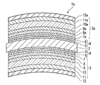
- FIG. 2 is a side sectional view schematically showing a second embodiment of the optical component of the present invention.
- reference numeral 1a is an optical component for a spectacle lens.
- This optical component 1a includes an inorganic multilayer film 3a disposed on the surface of the plastic substrate 2 in addition to the structure of the optical component 1 of the first embodiment having the inorganic multilayer film 3 on the back surface. . That is, in the optical component 1a of this embodiment, the inorganic multilayer film 3 is disposed on the back surface of the plastic substrate 2, and the inorganic multilayer film 3a is disposed on the surface.
- the functional thin film 4 is disposed between the surface of the plastic substrate 2 and the inorganic multilayer film 3a, as in the case of the back surface structure of the present embodiment. Also in this embodiment, the functional thin film 4 includes a primer layer 5 and a hard coat layer 6. In the present embodiment, as in the case of the back surface structure, a water / oil repellent film 12 is further provided on the inorganic multilayer film 3.
- the inorganic multilayer film 3a has a multilayer structure in which a plurality of high-refractive index inorganic materials and low-refractive index inorganic materials are alternately stacked on the plastic substrate 2 described above.
- the inorganic multilayer film 3a It has the same configuration. That is, the inorganic multilayer film 3a in the illustrated example has a five-layer structure in which five layers of high refractive index inorganic material and low refractive index inorganic material are alternately laminated on the plastic substrate 2 as described above.
- the inorganic multilayer film 3a, and the first layer 7a, the second layer 8a, the third layer 9a, the fourth layer 10a, and the fifth layer 11a constituting the inorganic multilayer film 3a are the back side inorganic multilayer film 3 and the inorganic multilayer film, respectively. Since it has the same configuration as the first layer 7, the second layer 8, the third layer 9, the fourth layer 10 and the fifth layer 11 constituting the film 3, the description thereof will be omitted. They may be the same or different as long as the limiting conditions of the present invention are satisfied.
- the manufacturing method of the present embodiment includes a step of forming the functional thin film 4 (primer layer 5 and hard coat layer 6) on the plastic substrate 2 by a method similar to the conventional method, and a step of heating the plastic substrate 2. After the plastic substrate 2 is adjusted to a predetermined temperature (for example, 70 ° C.) by heating, the step of forming the inorganic multilayer film 3 on the plastic substrate 2 and the formation of the water / oil repellent film 12 on the inorganic multilayer film 3 And a step of performing.
- a predetermined temperature for example, 70 ° C.
- the step of forming the inorganic multilayer film 3 is a process of alternately laminating a plurality of high refractive index inorganic materials and low refractive index inorganic materials to form a multilayer structure film.
- a low-refractive-index layer composed of the second layer 8 a high-refractive-index layer composed of a high-refractive-index inorganic material of the second layer 8, a low-refractive-index layer of the third layer 9, and a fourth layer 10
- the thick film of the high refractive index layer and the low refractive index layer of the fifth layer 11 are sequentially formed thereon.
- a vacuum deposition method is preferably used for forming each of the first to fifth layers.
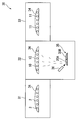
- FIG. 3 is a view showing an example of a vapor deposition apparatus 30 for forming the layers 7 to 11 of the inorganic multilayer film 3.
- the vapor deposition apparatus 30 includes a first film formation chamber 31, a second film formation chamber 32, and a third film formation chamber 33.
- Each of the first film forming chamber 31, the second film forming chamber 32, and the third film forming chamber 33 is configured so that the inside of each of the first film forming chamber 31, the second film forming chamber 32, and the third film forming chamber 33 is maintained in that state.
- the vapor deposition apparatus 30 can adjust the internal temperature of each of the first film forming chamber 31, the second film forming chamber 32, and the third film forming chamber 33 by temperature control means (not shown).
- the vapor deposition apparatus 30 includes a holding member 34 in each internal space of the first film formation chamber 31, the second film formation chamber 32, and the third film formation chamber 33.
- the holding member 34 has a curved upper surface (holding surface) and is configured to be rotatable, and holds a plurality of plastic substrates 2 on the upper surface.
- the vapor deposition source 35 of the vapor deposition apparatus 30 is disposed in a space inside the second film formation chamber 32.
- the vapor deposition source 35 includes a first vapor deposition source 35A and a second vapor deposition source 35B.
- a light source device 36 capable of irradiating the vapor deposition source 35 with a beam is disposed in the second film forming chamber 32.
- the light source device 36 can irradiate the vapor deposition source 35 with electrons and knock out the constituent particles of the vapor deposition source 35.
- the light source device 36 irradiates the second vapor deposition source 35 ⁇ / b> B with a beam to release SiO 2 vapor from the second vapor deposition source 35 ⁇ / b> B and supply the vapor onto the plastic substrate 2 held by the holding member 34. Evaporate. Thereby, the 1st layer 7, the 3rd layer 9, and the 5th layer 11 which are the low refractive index layers of the inorganic multilayer film 3 can be formed.
- the light source device 36 irradiates the first vapor deposition source 35 ⁇ / b > A with a beam, thereby releasing the vapor of ZrO 2 from the first vapor deposition source 35 ⁇ / b> A and supplying the vapor onto the plastic substrate 2 held by the holding member 34. And evaporate. Thereby, the second layer 8 and the fourth layer 10 which are high refractive index layers of the inorganic multilayer film 3 can be formed.
- the high refractive index inorganic material is formed on the plastic substrate 2 held by the holding member 34.
- layers made of a low refractive index inorganic material can be alternately formed and laminated.
- the average value of the reflectance in the wavelength range of 280 to 380 nm is 15% or less
- the fourth layer 10 as the high refractive index layer has an optical film thickness of 0.400 to 0.700 ⁇ . It is formed to be a thick film.
- the step of forming the inorganic multilayer film 3 includes the step of forming a film while performing ion beam assist on at least one of the layers constituting the inorganic multilayer film 3. May be included.
- the optical component manufacturing method of this embodiment includes such a step, so that a conductive film such as ITO or metal is disposed between the high refractive index inorganic material and the low refractive index inorganic material constituting the inorganic multilayer film. Established.
- FIG. 4 is a diagram showing an example of a film forming apparatus 30a for performing ion beam assist.
- the film forming apparatus 30a has a configuration in which an ion gun 37 is provided in the second film forming chamber of the film forming apparatus 30 shown in FIG.
- a conductor film such as ITO or metal is disposed between the fourth layer 10 which is a high refractive index layer and the fifth layer 11 which is a low refractive index layer constituting the inorganic multilayer film 3.
- film formation is performed while performing ion beam assist.
- at least one of the layers constituting the inorganic multilayer film 3 in the film forming chamber 32 may be formed while performing ion beam assist, and the target to be subjected to ion beam assist is not limited to the conductor film.
- the second film forming chamber of the film forming apparatus 30a includes a holding member 34 that holds the base material on which the fourth layer 10 is formed on the plastic base material 2, a vapor deposition source 35a, and a vapor deposition source.
- An ion gun 37 and a light source device 36 which are arranged apart from 35a are mainly configured. Further, the inside of the film forming apparatus 30a is depressurized to almost vacuum, so that the periphery of the plastic substrate 2 can be maintained in a vacuum atmosphere.
- an atmospheric gas supply source such as a gas cylinder is connected to the film forming apparatus 30a, and the inside of the vacuum vessel is in a low pressure state such as a vacuum, and an oxygen gas, argon gas, or other inert gas atmosphere, or in addition, an inert gas atmosphere containing oxygen can be formed.
- the vapor deposition source 35a includes, for example, ITO.
- ITO Indium Tin Oxide
- the light source device 36 irradiates the vapor deposition source 35 a with a beam, the gasified ITO is emitted from the vapor deposition source 35 a and supplied to the plastic substrate 2 held by the holding member 34. Thereby, a conductor film made of ITO can be formed on the fourth layer 10.
- the ion gun 37 is configured such that a gas to be ionized is introduced into the second film forming chamber 32 and a lead electrode is provided on the front surface.
- the light source device 36 has the same configuration as the ion gun 37, and can irradiate the vapor deposition source 35a with electrons to knock out the constituent particles of the vapor deposition source 35a.
- the constituent particles of the vapor deposition source 35a can be knocked out by applying a voltage to the vapor deposition source 35a with a high frequency coil or the like.
- the light source device 36 may be omitted.
- an ITO conductive film is formed on the fourth layer 10 of the high refractive index layer on the plastic substrate 2 using the film forming apparatus 30a having the above-described configuration.
- an ITO vapor deposition source 35 a is used, and ions irradiated from the ion gun 37 can be irradiated onto the upper surface of the holding member 34.
- the inside of the film forming chamber 32 containing the plastic substrate 2 is evacuated to make a reduced pressure atmosphere. Then, the ion gun 37 and the light source device 36 are operated.
- the constituent particles of the vapor deposition source 35a are knocked out and fly onto the fourth layer 10. Then, the constituent particles knocked out from the vapor deposition source 35 a are deposited on the fourth layer 10, and at the same time, argon ions are irradiated from the ion gun 37.
- the ion beam assist is preferably performed using at least one gas selected from an inert gas, an oxygen gas, and a mixed gas of an inert gas and an oxygen gas.
- the inert gas is preferably argon.
- the water / oil repellent film 12 is formed thereon to form the optical component 1.
- a wet method such as a dipping method, a spin coat method and a spray method, or a dry method such as a vacuum deposition method.
- the dipping method is common and is often used.
- the inorganic multilayer film 3 is formed in a solution obtained by dissolving a fluorine-substituted alkyl group-containing organosilicon compound in an organic solvent, the optical component is immersed, pulled up under certain conditions, and dried to form a film.
- the organic solvent perfluorohexane, perfluoro-4-methoxybutane, perfluoro-4-ethoxybutane, metaxylene hexafluoride, or the like is used.
- the dilution concentration with an organic solvent is preferably 0.01 to 0.5% by weight, more preferably 0.03 to 0.1% by weight. If the concentration is too low, the water / oil repellent layer 12 having a sufficient film thickness cannot be obtained, and if the concentration is too high, uneven coating tends to occur and the material cost increases. Of the dry methods, vacuum deposition is often used. This method is a method of forming the water- and oil-repellent film 12 by heating and evaporating the fluorine-substituted alkyl group-containing organosilicon compound in a vacuum chamber.
- the average value of the reflectance of the inorganic multilayer film 3 in the wavelength range of 280 to 380 nm is 20% or less, and the fourth layer 10 of the high refractive index layer is used. Since the optical film thickness is set to 0.400 to 0.700 ⁇ as the optical film thickness, as described above, both the reflection characteristics in the ultraviolet region and the visibility in the visible region should be ensured. Can do. Moreover, in the manufacturing method of an optical component, such a well-balanced and excellent optical component can be reliably provided.
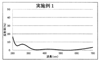
- Example 1 The lens is set in a rotating dome provided in the vacuum chamber, the temperature in the vacuum chamber is heated to 70 degrees, the pressure is exhausted until the pressure reaches 1.0 ⁇ 10 ⁇ 3 Pa, an acceleration voltage of 500 V, an acceleration current After performing Ar ion beam cleaning for 60 seconds under the condition of 100 mA, the first layer of SiO 2 (refractive index: 1.47) with an optical film thickness of 0.080 ⁇ and the second layer of ZrO 2 is sequentially formed from the plastic substrate side.
- Refractive index 2.00 is optical film thickness 0.080 ⁇
- third layer SiO 2 (refractive index 1.47) is optical film thickness 0.050 ⁇
- fourth layer ZrO 2 (refractive index 2.00).
- Example 2 The lens is set in a rotating dome provided in the vacuum chamber, the temperature in the vacuum chamber is heated to 70 degrees, the pressure is exhausted until the pressure reaches 1.0 ⁇ 10 ⁇ 3 Pa, an acceleration voltage of 500 V, an acceleration current After performing Ar ion beam cleaning for 60 seconds under the condition of 100 mA, the first layer of SiO 2 (refractive index: 1.47) with an optical film thickness of 0.080 ⁇ and the second layer of ZrO 2 is sequentially formed from the plastic substrate side.
- Refractive index 2.00 is optical film thickness 0.080 ⁇
- third layer SiO 2 (refractive index 1.47) is optical film thickness 0.060 ⁇
- fourth layer ZrO 2 (refractive index 2.00).
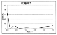
- the reflection spectral characteristics of the multilayer film of Example 2 thus obtained are shown in FIG. 6, and the configuration and film characteristics of the multilayer film of Example 2 are shown in Table 1.
- the multilayer film of Example 2 has a reflectance in the vicinity of 280 nm and 780 nm as a result of the ITO film provided between the fourth layer of ZrO 2 and the sixth layer of SiO 2.
- the reflection spectral characteristic balanced in both the visible region and the ultraviolet region is shown.
- Example 3 The lens is set in a rotating dome provided in the vacuum chamber, the temperature in the vacuum chamber is heated to 70 degrees, the pressure is exhausted until the pressure reaches 1.0 ⁇ 10 ⁇ 3 Pa, an acceleration voltage of 500 V, an acceleration current After Ar ion beam cleaning was performed for 60 seconds under the condition of 100 mA, the ZrO 2 (refractive index of 2.00) of the first layer was sequentially formed from the plastic substrate side with an optical film thickness of 0.050 ⁇ and the SiO 2 of the second layer. (Refractive index 1.47) is the optical film thickness 0.050 ⁇ , the third layer ZrO 2 (refractive index 2.00) is the optical film thickness 0.040 ⁇ , and the fourth layer SiO 2 (refractive index 1.47).
- Example 4 The lens is set in a rotating dome provided in the vacuum chamber, the temperature in the vacuum chamber is heated to 70 degrees, the pressure is exhausted until the pressure reaches 1.0 ⁇ 10 ⁇ 3 Pa, an acceleration voltage of 500 V, an acceleration current After performing Ar ion beam cleaning for 60 seconds under the condition of 100 mA, the first layer of SiO 2 (refractive index: 1.47) with an optical film thickness of 0.150 ⁇ and the second layer of ZrO 2 is sequentially formed from the plastic substrate side.
- Refractive index 2.00 is optical film thickness 0.060 ⁇
- third layer SiO 2 (refractive index 1.47) is optical film thickness 0.100 ⁇
- fourth layer ZrO 2 (refractive index 2.00).
- the multilayer film of Example 4 With an optical film thickness of 0.440 ⁇ and a fifth layer of SiO 2 (refractive index of 1.47) with an optical film thickness of 0.270 ⁇ . Note that ⁇ is 500 nm as the design center wavelength.
- the reflection spectral characteristics of the multilayer film of Example 4 thus obtained are shown in FIG. 8, and the configuration and film characteristics of the multilayer film of Example 4 are shown in Table 1. As is clear from FIG. 8, the multilayer film of Example 4 has a little higher reflectance near 280 nm and 780 nm, but has a reflection spectral characteristic similar to that shown in FIG. You can see that
- Example 5 The lens is set in a rotating dome provided in the vacuum chamber, the temperature in the vacuum chamber is heated to 70 degrees, the pressure is exhausted until the pressure reaches 1.0 ⁇ 10 ⁇ 3 Pa, an acceleration voltage of 500 V, an acceleration current After Ar ion beam cleaning was performed for 60 seconds under the condition of 100 mA, the ZrO 2 (refractive index of 2.00) of the first layer was sequentially formed from the plastic substrate side with an optical film thickness of 0.050 ⁇ and the SiO 2 of the second layer. (Refractive index 1.47) is the optical film thickness 0.050 ⁇ , the third layer ZrO 2 (refractive index 2.00) is the optical film thickness 0.090 ⁇ , and the fourth layer SiO 2 (refractive index 1.47).
- Example 6> The lens is set in a rotating dome provided in the vacuum chamber, the temperature in the vacuum chamber is heated to 70 degrees, the pressure is exhausted until the pressure reaches 1.0 ⁇ 10 ⁇ 3 Pa, an acceleration voltage of 500 V, an acceleration current After Ar ion beam cleaning was performed for 60 seconds under the condition of 100 mA, the ZrO 2 (refractive index of 2.00) of the first layer was sequentially formed from the plastic substrate side with an optical film thickness of 0.040 ⁇ and the second layer of SiO 2. (Refractive index 1.47) is the optical film thickness 0.070 ⁇ , the third layer ZrO 2 (refractive index 2.00) is the optical film thickness 0.060 ⁇ , and the fourth layer SiO 2 (refractive index 1.47).
- the reflection spectral characteristics of the multilayer film of Example 6 thus obtained are shown in FIG. 10, and the configuration and film characteristics of the multilayer film of Example 6 are shown in Table 2. As is clear from FIG.
- the multilayer film of Example 6 has a slightly higher reflectance near 280 nm and does not have a peak (extreme value) in the ultraviolet region, but the average reflectance is sufficiently low, and the visible region is It can be seen that the reflection spectral characteristic similar to that shown in FIG.
- Example 7 The lens is set in a rotating dome provided in the vacuum chamber, the temperature in the vacuum chamber is heated to 70 degrees, the pressure is exhausted until the pressure reaches 1.0 ⁇ 10 ⁇ 3 Pa, an acceleration voltage of 500 V, an acceleration current
- the first layer of TiO 2 (refractive index of 2.49) is sequentially formed from the plastic substrate side with an optical film thickness of 0.050 ⁇ and a second layer of MgF 2 ( Refractive index 1.38) is optical thickness 0.050 ⁇
- third layer TiO 2 (refractive index 2.49) is optical thickness 0.410 ⁇
- fourth layer MgF 2 (refractive index 1.38) is optical.
- the optical film thickness is 0.020 ⁇
- the fifth layer TiO 2 (refractive index 2.49) is the optical film thickness 0.080 ⁇
- the sixth layer SiO 2 (refractive index 1.47) is the optical film thickness 0.220 ⁇ .
- ⁇ is 500 nm as the design center wavelength.
- the reflection spectral characteristics of the multilayer film of Example 7 thus obtained are shown in FIG. 11, and the configuration and film characteristics of the multilayer film of Example 7 are shown in Table 2.
- the multilayer film of Example 7 uses TiO 2 for the high refractive index layer and MgF 2 and SiO 2 for the low refractive index layer. It can be seen that the reflection spectral characteristic similar to that shown in FIG.
- the SiO 2 (refractive index of 1.47) of the first layer is sequentially formed from the plastic substrate side with an optical film thickness of 0.110 ⁇
- the second layer of ZrO 2 (refractive index 2.00) has an optical thickness of 0.150 ⁇
- the third layer of SiO 2 (refractive index 1.47) has an optical thickness of 0.080 ⁇
- the fourth layer of ZrO 2 A (refractive index of 2.00) was laminated with an optical film thickness of 0.230 ⁇
- a fifth layer of SiO 2 (refractive index of 1.47) was laminated with an optical film thickness of 0.280 ⁇ .
- ⁇ is 500 nm as the design center wavelength.
- the reflection spectral characteristics of the multilayer film of Comparative Example 1 thus obtained are shown in FIG. 12, and the configuration and film characteristics of the multilayer film of Comparative Example 1 are shown in Table 3.
- the multilayer film of Comparative Example 1 is a general antireflection film used for spectacle lenses, and has a large reflectance peak in the ultraviolet region, and is shown in FIG. It can be seen that the reflection spectral characteristic is completely different from the reflection spectral characteristic.
- the SiO 2 (refractive index: 1.47) of the first layer is sequentially formed from the plastic substrate side with an optical film thickness of 0.150 ⁇
- the second layer ZrO 2 (refractive index 2.00) has an optical film thickness of 0.150 ⁇
- the third layer SiO 2 (refractive index 1.47) has an optical film thickness of 0.060 ⁇
- a (refractive index of 2.00) was laminated with an optical film thickness of 0.350 ⁇
- a fifth layer of SiO 2 (refractive index of 1.47) was laminated with an optical film thickness of 0.270 ⁇ .
- ⁇ is 500 nm as the design center wavelength.
- the reflection spectral characteristics of the multilayer film of Comparative Example 2 thus obtained are shown in FIG. 13, and the configuration and film characteristics of the multilayer film of Comparative Example 2 are shown in Table 3.
- the multilayer film of Comparative Example 2 has a large reflectance peak in the ultraviolet region because the thickness of the thick film of the high refractive index layer is a little thinner than specified. It can be seen that the reflection spectral characteristic completely different from the reflection spectral characteristic shown in FIG.
- ⁇ Comparative Example 3> The lens is set in a rotating dome provided in the vacuum chamber, the temperature in the vacuum chamber is heated to 70 degrees, the pressure is exhausted until the pressure reaches 1.0 ⁇ 10 ⁇ 3 Pa, an acceleration voltage of 500 V, an acceleration current After Ar ion beam cleaning was performed for 60 seconds under the condition of 100 mA, the ZrO 2 (refractive index of 2.00) of the first layer was sequentially formed from the plastic substrate side with an optical film thickness of 0.040 ⁇ and the second layer of SiO 2. (Refractive index 1.47) is the optical film thickness 0.140 ⁇ , the third layer ZrO 2 (refractive index 2.00) is the optical film thickness 0.050 ⁇ , and the fourth layer SiO 2 (refractive index 1.47).
- the multilayer film of Comparative Example 3 has a large reflectance peak in the ultraviolet region because the thickness of the thick film of the high refractive index layer is larger than specified, and FIG. It can be seen that the reflection spectral characteristic completely different from the reflection spectral characteristic shown in FIG.
- Comparative Example 2 is a design in which the film thickness of the high refractive index layer is smaller (thin) than that of the present invention
- Comparative Example 3 is a design in which the film thickness of the high refractive index layer is larger (thicker) than that of the present invention.
- Comparative Example 2 the average reflectance of ultraviolet rays at an incident angle of 0 degrees and 35 degrees is 15% or more, and in Comparative Example 3, the average reflectance of ultraviolet rays at an incident angle of 0 degrees is 15% or more. It can be seen that the hue angle of light is 293 degrees, which greatly deviates from the hue angle of reflected light in a general spectacle lens.
- Example 4 is a design in which the ratio of the highly bent layer to the total film thickness of the multilayer film is small.
- the characteristics in the visible region and the average reflectance in the ultraviolet region are within the specified range, but the luminous reflectance and the average reflectance in the ultraviolet region are slightly inferior to those in Examples 1 to 3. I understand.
- Example 5 is a design in which a thick film of a high refractive index layer is installed in the vicinity of the middle of the multilayer film. Also in this case, the luminous reflectance is larger than in Examples 1 to 3. From the above results, the effect of the present invention is clear.
- the multilayer film disposed on the back surface of the lens is within the specified range of the present invention, the surface reflection in the ultraviolet region is not impaired and the characteristics of the existing antireflection film are not impaired. It is apparent that an optical component capable of suppressing the incidence on the eyeball due to the reflection of the ultraviolet light incident from the rear and the manufacturing method thereof can be provided depending on the characteristics.
- the anti-glare effect, good visibility, and low surface reflection characteristics in the ultraviolet region can suppress incidence on the eyeball due to reflection of ultraviolet light incident from the rear. It is clear that an optical component and a manufacturing method thereof can be provided.
Landscapes
- Physics & Mathematics (AREA)
- General Physics & Mathematics (AREA)
- Optics & Photonics (AREA)
- Health & Medical Sciences (AREA)
- Ophthalmology & Optometry (AREA)
- General Health & Medical Sciences (AREA)
- Chemical & Material Sciences (AREA)
- Inorganic Chemistry (AREA)
- Surface Treatment Of Optical Elements (AREA)
- Eyeglasses (AREA)
- Laminated Bodies (AREA)
Abstract
The purpose of the present invention is to provide an optical component having good visibility and which is also effective at preventing eye disease, and the present invention is an optical component in which a multilayer film is provided on both surfaces of a plastic lens, a multilayer film provided on a back surface having an average reflectance of 15% or less in a wavelength region of 280 nm to 380 nm when the angle of incidence is 0 degrees to 45 degrees, the multilayer film provided on the back surface comprising three or more high-refractive-index layers and low-refractive-index layers superposed on each other, and at least one high-refractive-index layer in the multilayer film provided on the back surface being a thick film having an optical film thickness of 0.400-0.700 λ.
Description
本発明は、眼鏡レンズ等の光学部品に関する。
The present invention relates to an optical component such as a spectacle lens.
近年、眼鏡レンズでは、軽量で耐衝撃性に優れ、かつ染色しやすいとの利点からプラスチックレンズが多用されている。眼鏡レンズに使用されるプラスチックレンズには、表面反射を防止する目的で、通常、その両面に反射防止膜が施されている。通常用いられる眼鏡レンズ用反射防止膜は、一般的に380nm~780nmの可視領域全域にわたって、低い反射特性(広帯域低反射特性)を有する。
眼鏡レンズ等の光学部品においては、従来、プラスチックの基材と、その基材上に配置される反射防止膜とを備えた光学部品が知られている。 In recent years, plastic lenses are frequently used for spectacle lenses because of their advantages of being lightweight, excellent in impact resistance and easy to dye. In order to prevent surface reflection, plastic lenses used for spectacle lenses are usually provided with antireflection films on both sides. Generally used antireflection films for spectacle lenses generally have low reflection characteristics (broadband low reflection characteristics) over the entire visible region of 380 nm to 780 nm.
2. Description of the Related Art Conventionally, optical parts such as eyeglass lenses are known that include a plastic base material and an antireflection film disposed on the base material.
一方、280nm~380nmの紫外線も眼球に対する暴露が網膜などの損傷の原因になることが知られている。屋外での長時間の紫外線暴露が角膜炎や白内障等の原因となるので、紫外領域の光をカットすることが望ましいとされている。
紫外線をカットする手段としては、サングラスなどの染色レンズが知られているが、眼鏡レンズにおいては、レンズ本体に紫外線吸収剤を含有させているものや、紫外線カットコーティングが施されているものもある。
このようなサングラスや、従来の眼鏡レンズにおいては、眼鏡レンズの表面(前面;眼球と逆側の面)から入射してくる紫外線を低減若しくは遮蔽することはできる。しかし、これらの方法では、眼鏡レンズの裏面(後面;眼球側の面)で反射される紫外線への制御が考慮されておらず、眼鏡レンズ装用者の後方、斜め横から入射し、レンズの裏面で反射されて眼球に到達する紫外光がそのまま眼球に入射されてしまい、眼球を損傷してしまう可能性がある。 On the other hand, ultraviolet rays of 280 nm to 380 nm are known to cause damage to the retina due to exposure to the eyeball. It is considered desirable to cut off light in the ultraviolet region because long-term exposure to ultraviolet rays outdoors causes keratitis, cataracts, and the like.
As means for cutting off ultraviolet rays, dyed lenses such as sunglasses are known. However, some spectacle lenses contain a UV absorber in the lens body and some are provided with UV cut coating. .
In such sunglasses and conventional spectacle lenses, it is possible to reduce or block ultraviolet rays incident from the front surface (front surface; the surface opposite to the eyeball) of the spectacle lens. However, these methods do not take into account the control of ultraviolet rays reflected from the back surface of the spectacle lens (rear surface: the surface on the eyeball side). There is a possibility that the ultraviolet light that is reflected by and reaches the eyeball is directly incident on the eyeball and may damage the eyeball.
このため、眼鏡レンズの裏面に、紫外線の反射を抑制する反射防止膜が形成された眼鏡用レンズが提案されている(特許文献1及び2参照)。
特許文献1には、眼鏡レンズの裏面に、280~315nm及び420~680nmの波長領域のすべての光線に対する表面反射率がレンズ基材自身の表面反射率より小さい無機膜を形成した眼鏡用レンズが開示されている。
特許文献1に開示の眼鏡用レンズは、視線方向後方よりの紫外線、特に遠紫外線がレンズの裏面で反射することが確実に防止され、これにより、眼内に侵入する紫外線の光量が低減されるとしている。 For this reason, a spectacle lens in which an antireflection film that suppresses reflection of ultraviolet rays is formed on the back surface of the spectacle lens has been proposed (see Patent Documents 1 and 2).
Patent Document 1 discloses a spectacle lens in which an inorganic film having a surface reflectance smaller than that of the lens base material itself is formed on the back surface of the spectacle lens with respect to all rays in the wavelength region of 280 to 315 nm and 420 to 680 nm. It is disclosed.
In the spectacle lens disclosed in Patent Document 1, it is possible to reliably prevent ultraviolet rays from the rear in the line of sight, particularly far ultraviolet rays, from being reflected from the back surface of the lens, thereby reducing the amount of ultraviolet rays entering the eye. It is said.
また、特許文献2には、眼鏡レンズの裏面に、屈折率1.6以上の少なくとも1つの高屈折率層と屈折率1.5以下の少なくとも1つの低屈折率層との積層体からなる多層反射防止膜が形成された眼鏡レンズであって、可視域の平均反射率Rmが1.15%以下、視感反射率Rvが1%以下、入射角30°及び45°である時の280nm~380nmの波長領域における重み付け平均反射率Ruv(ISO 13666:1998 Standard)が5%以下であり、多層膜は、3層以上7層以下であり、20nm以下のITOを含有し、多層膜の外層がシリカベース膜である眼鏡レンズを開示している。
特許文献2に開示の眼鏡用レンズでは、レンズの裏面に、可視域及び紫外域において良好な反射防止性能を持つ紫外線及び反射防止膜が形成されるとしている。Patent Document 2 discloses a multilayer structure comprising a laminated body of at least one high refractive index layer having a refractive index of 1.6 or more and at least one low refractive index layer having a refractive index of 1.5 or less on the back surface of the spectacle lens. An eyeglass lens having an antireflection film, which has an average reflectance Rm in the visible range of 1.15% or less, a luminous reflectance Rv of 1% or less, and incident angles of 30 ° and 45 °, The weighted average reflectance Ruv (ISO 13666: 1998 Standard) in the wavelength region of 380 nm is 5% or less, the multilayer film is 3 to 7 layers, contains ITO of 20 nm or less, and the outer layer of the multilayer film is An eyeglass lens that is a silica-based film is disclosed.
In the spectacle lens disclosed inPatent Document 2, ultraviolet and antireflection films having good antireflection performance in the visible region and the ultraviolet region are formed on the back surface of the lens.
特許文献2に開示の眼鏡用レンズでは、レンズの裏面に、可視域及び紫外域において良好な反射防止性能を持つ紫外線及び反射防止膜が形成されるとしている。
In the spectacle lens disclosed in
ところで、特許文献1及び2に開示の眼鏡レンズでは、高屈折率層と低屈折率層との重ね合わせからなる多層膜によって一定程度の紫外線の反射防止性能を得ることはできるものの、耐熱性、耐クラック性及び耐久性等の性能の劣化を抑えて、可視域及び紫外域の両方において良好な反射防止性能を少ない層数で得ることが容易ではないという問題があった。
By the way, in the spectacle lenses disclosed in Patent Documents 1 and 2, although a certain degree of antireflection performance of ultraviolet rays can be obtained by a multilayer film formed by superposing a high refractive index layer and a low refractive index layer, There has been a problem that it is not easy to obtain good antireflection performance with a small number of layers in both the visible region and the ultraviolet region while suppressing deterioration in performance such as crack resistance and durability.
本発明は、上記事情に鑑みてなされたものであり、眼病予防にも効果的で、かつ、視認性が良好な光学部品を提供することを目的とする。
即ち、本発明の目的は、上記従来技術の問題点を解消し、耐熱性、耐クラック性及び耐久性等の性能を劣化を抑え、可視域において光学性能の低下のない、紫外域において反射防止性能に優れた光学部品を提供するにある。 The present invention has been made in view of the above circumstances, and an object of the present invention is to provide an optical component that is effective in preventing eye diseases and has good visibility.
That is, the object of the present invention is to eliminate the above-mentioned problems of the prior art, suppress degradation of performance such as heat resistance, crack resistance and durability, and prevent reflection in the ultraviolet region without any deterioration in optical performance in the visible region. It is to provide an optical component with excellent performance.
上記目的を達成するために、本発明の光学部品は、プラスチックレンズの少なくとも裏面に多層膜を備えた光学部品であって、前記プラスチックレンズの裏面に配設された前記多層膜は、入射角が0度~45度の時の280nm~380nmの波長領域における平均反射率が15%以下であり、前記裏面に配設された前記多層膜は、高屈折率物質からなる高屈折率層と低屈折率物質からなる低屈折率層との3層以上の重ね合わせからなり、前記裏面に配設された前記多層膜中の少なくとも1つの高屈折率層は、その光学的膜厚が0.400~0.700λである厚膜であることを特徴とする。
In order to achieve the above object, an optical component of the present invention is an optical component including a multilayer film on at least the back surface of a plastic lens, and the multilayer film disposed on the back surface of the plastic lens has an incident angle. The average reflectance in the wavelength region of 280 nm to 380 nm at 0 ° to 45 ° is 15% or less, and the multilayer film disposed on the back surface includes a high refractive index layer made of a high refractive index material and a low refractive index. The optical film thickness of the at least one high refractive index layer in the multilayer film disposed on the back surface is three or more layers with a low refractive index layer made of a refractive index material. It is a thick film having a thickness of 0.700λ.
ここで、前記裏面に配設された前記多層膜の全体の膜厚に対する前記高屈折率層が占める割合が45%より大きいことが好ましい。
また、前記裏面に配設された前記多層膜は、入射角が0度~45度の時の280nm~380nmの波長領域における前記平均反射率が10%以下であることが好ましい。
また、前記裏面に配設された前記多層膜の反射光の視感反射率が1.5%以下、かつ、その色相角が120~220度であることが好ましい。 Here, the ratio of the high refractive index layer to the total film thickness of the multilayer film disposed on the back surface is preferably greater than 45%.
The multilayer film disposed on the back surface preferably has an average reflectance of 10% or less in a wavelength region of 280 nm to 380 nm when the incident angle is 0 degree to 45 degrees.
Further, it is preferable that a luminous reflectance of reflected light of the multilayer film disposed on the back surface is 1.5% or less and a hue angle thereof is 120 to 220 degrees.
また、前記厚膜である1つの高屈折率層は、前記裏面に配設された前記多層膜中の前記高屈折率層の中で、前記プラスチックレンズの基材から最も遠い層であることが好ましい。
また、前記裏面に配設された前記多層膜を構成する前記高屈折率層と低屈折率層との間に、導電体膜、金属膜又は可視光の吸収膜を備えたことが好ましい。
また、前記プラスチックレンズが、紫外線を吸収する機能を有することが好ましい。 Further, the one high refractive index layer that is the thick film is a layer farthest from the base material of the plastic lens among the high refractive index layers in the multilayer film disposed on the back surface. preferable.
Moreover, it is preferable that a conductor film, a metal film, or a visible light absorbing film is provided between the high refractive index layer and the low refractive index layer constituting the multilayer film disposed on the back surface.
The plastic lens preferably has a function of absorbing ultraviolet rays.
また、前記プラスチックレンズの基材は、着色されていても良い。また、着色された前記プラスチックレンズの基材の透過率は、5~85%であることが好ましい。
また、前記280nm~380nmの前記波長領域において、波長に対する前記裏面に配設された前記多層膜の反射率を表す分光特性曲線は、1つの極値を持つ曲線、又は極値を持たない単調な曲線であり、前記分光特性曲線が前記1つの極値を持つ曲線である場合には、前記1つの極値は、20%以下の反射率であることが好ましい。
前記多層膜は、前記プラスチックレンズの裏面に加え、さらに、前記プラスチックレンズの表面に配設されても良い。 The base material of the plastic lens may be colored. The transmittance of the colored plastic lens substrate is preferably 5 to 85%.
Further, in the wavelength region of 280 nm to 380 nm, the spectral characteristic curve representing the reflectance of the multilayer film disposed on the back surface with respect to the wavelength is a curve having one extreme value or a monotone having no extreme value. When the spectral characteristic curve is a curve having the one extreme value, the one extreme value is preferably a reflectance of 20% or less.
The multilayer film may be disposed on the surface of the plastic lens in addition to the back surface of the plastic lens.
本発明によれば、以上のように構成されている光学多層膜によって従来の眼鏡レンズと可視域の特性において変わらず良好な視認性を維持したまま充分な紫外線カット効果を得ることができる。
また、本発明によれば、以上のように構成されているので、耐熱性、耐クラック性及び耐久性等の性能の劣化を抑え、可視域において光学性能の低下のない、紫外域において反射防止性能に優れた光学部品を提供することができる。
さらに、本発明によれば、眼球内に入射される紫外線が低減され、眩しさを低減し、見え易く、疲労、眼病予防にも効果的な光学特性を有した光学部品を提供することが可能となる。 According to the present invention, the optical multilayer film configured as described above can obtain a sufficient ultraviolet ray cutting effect while maintaining good visibility without changing in the characteristics of the visible region as compared with the conventional spectacle lens.
In addition, according to the present invention, since it is configured as described above, it suppresses deterioration of performance such as heat resistance, crack resistance and durability, and does not deteriorate optical performance in the visible region, and prevents reflection in the ultraviolet region. An optical component having excellent performance can be provided.
Furthermore, according to the present invention, it is possible to provide an optical component having reduced optical intensity in the eyeball, reduced glare, easy to see, and effective optical properties for fatigue and eye disease prevention. It becomes.
以下、本発明に係る光学部品を添付の図面に示す好適実施形態に基づいて詳細に説明する。
なお、以下に示す好適実施形態は、発明の趣旨をより良く理解させるために具体的に説明するものであり、特に指定のない限り、本発明を限定するものではない。 DESCRIPTION OF EXEMPLARY EMBODIMENTS Hereinafter, an optical component according to the invention will be described in detail based on preferred embodiments shown in the accompanying drawings.
The preferred embodiments described below are specifically described for better understanding of the gist of the invention, and do not limit the present invention unless otherwise specified.
(1)第1実施形態
図1は、本発明の第1実施形態に係る光学部品の一例を模式的に示す側断面図である。
同図に示す光学部品1は、眼鏡レンズ用の光学部品であり、プラスチック基材2と、プラスチック基材2の裏面に配設された無機多層膜3とを備えて構成されている。
本実施形態の光学部品1では、プラスチック基材2の裏面と無機多層膜3との間には機能性薄膜4が配設されており、この機能性薄膜4は、プライマ層5とハードコート層6とからなっている。また、本実施形態では、さらに、無機多層膜3の上には撥水撥油膜12が設けられている。この撥水撥油膜12については後述する。
なお、本実施形態においては、プラスチック基材2の表面にも、無機多層膜3及び機能性薄膜4に相当する任意の膜が形成されているが、かかる膜の図示及び説明を省略する。 (1) 1st Embodiment FIG. 1: is a sectional side view which shows typically an example of the optical component which concerns on 1st Embodiment of this invention.
An optical component 1 shown in FIG. 1 is an optical component for a spectacle lens, and includes aplastic substrate 2 and an inorganic multilayer film 3 disposed on the back surface of the plastic substrate 2.
In the optical component 1 of the present embodiment, a functionalthin film 4 is disposed between the back surface of the plastic substrate 2 and the inorganic multilayer film 3, and the functional thin film 4 includes a primer layer 5 and a hard coat layer. It consists of six. In this embodiment, a water / oil repellent film 12 is further provided on the inorganic multilayer film 3. The water / oil repellent film 12 will be described later.
In the present embodiment, arbitrary films corresponding to theinorganic multilayer film 3 and the functional thin film 4 are also formed on the surface of the plastic substrate 2, but illustration and description of such films are omitted.
図1は、本発明の第1実施形態に係る光学部品の一例を模式的に示す側断面図である。
同図に示す光学部品1は、眼鏡レンズ用の光学部品であり、プラスチック基材2と、プラスチック基材2の裏面に配設された無機多層膜3とを備えて構成されている。
本実施形態の光学部品1では、プラスチック基材2の裏面と無機多層膜3との間には機能性薄膜4が配設されており、この機能性薄膜4は、プライマ層5とハードコート層6とからなっている。また、本実施形態では、さらに、無機多層膜3の上には撥水撥油膜12が設けられている。この撥水撥油膜12については後述する。
なお、本実施形態においては、プラスチック基材2の表面にも、無機多層膜3及び機能性薄膜4に相当する任意の膜が形成されているが、かかる膜の図示及び説明を省略する。 (1) 1st Embodiment FIG. 1: is a sectional side view which shows typically an example of the optical component which concerns on 1st Embodiment of this invention.
An optical component 1 shown in FIG. 1 is an optical component for a spectacle lens, and includes a
In the optical component 1 of the present embodiment, a functional
In the present embodiment, arbitrary films corresponding to the
プラスチック基材2は、例えば透明なプラスチックであるアクリル系樹脂、チオウレタン系樹脂、メタクリル系樹脂、アリル系樹脂、エピスルフィド系樹脂、ポリカーボネート系樹脂、ポリウレタン系樹脂、ポリエステル系樹脂、ポリスチレン系樹脂、エピスルフィド樹脂、ポリエ-テルサルホン樹脂ポリ4-メチルペンテン-1樹脂、ジエチレングリコールビスアリルカーボネート樹脂(CR-39)、ポリ塩化ビニル樹脂、ハロゲン含有共重合体、及びイオウ含有共重合体等によって形成されたものである。また、本実施形態では、プラスチック基材2の屈折率(nd)としては、例えば1.50、1.60、1.67、及び1.74のうちから選択されたものが用いられる。なお、プラスチック基材2の屈折率を1.6以上にする場合、プラスチック基材2としては、アリルカーボネート系樹脂、アクリレート系樹脂、メタクリレート系樹脂、及びチオウレタン系樹脂等を使用することが好ましい。
また、プラスチック基材2は、紫外線を吸収する機能を有することが好ましい。即ち、プラスチック基材2を構成する樹脂中に、紫外線吸収剤が含まれていることが好ましい。または、プラスチック基材2の面に配設される機能性薄膜4中に、紫外線吸収剤が含まれていてもよい。かかる場合には、機能性薄膜4中の紫外線吸収剤成分がプラスチック基材2に含浸する。
更に、プラスチック基材2は透光性を有していれば透明でなくてもよく、着色されていてもよい。着色されたプラスチック基材2の透過率は、5~85%であることが好ましい。 Theplastic substrate 2 is, for example, a transparent plastic such as acrylic resin, thiourethane resin, methacrylic resin, allyl resin, episulfide resin, polycarbonate resin, polyurethane resin, polyester resin, polystyrene resin, episulfide. Resin, polyethersulfone resin poly-4-methylpentene-1 resin, diethylene glycol bisallyl carbonate resin (CR-39), polyvinyl chloride resin, halogen-containing copolymer, sulfur-containing copolymer, etc. is there. In the present embodiment, the refractive index (nd) of the plastic substrate 2 is selected from, for example, 1.50, 1.60, 1.67, and 1.74. When the refractive index of the plastic substrate 2 is 1.6 or more, it is preferable to use an allyl carbonate resin, an acrylate resin, a methacrylate resin, a thiourethane resin, or the like as the plastic substrate 2. .
Theplastic substrate 2 preferably has a function of absorbing ultraviolet rays. That is, it is preferable that the resin constituting the plastic substrate 2 contains an ultraviolet absorber. Alternatively, the functional thin film 4 disposed on the surface of the plastic substrate 2 may contain an ultraviolet absorber. In such a case, the plastic substrate 2 is impregnated with the ultraviolet absorbent component in the functional thin film 4.
Furthermore, theplastic substrate 2 may not be transparent as long as it has translucency, and may be colored. The transmittance of the colored plastic substrate 2 is preferably 5 to 85%.
また、プラスチック基材2は、紫外線を吸収する機能を有することが好ましい。即ち、プラスチック基材2を構成する樹脂中に、紫外線吸収剤が含まれていることが好ましい。または、プラスチック基材2の面に配設される機能性薄膜4中に、紫外線吸収剤が含まれていてもよい。かかる場合には、機能性薄膜4中の紫外線吸収剤成分がプラスチック基材2に含浸する。
更に、プラスチック基材2は透光性を有していれば透明でなくてもよく、着色されていてもよい。着色されたプラスチック基材2の透過率は、5~85%であることが好ましい。 The
The
Furthermore, the
機能性薄膜4は、上述したようにプラスチック基材2と無機多層膜3との間に配置されたもので、プラスチック基材2に接して配設されたプライマ層5と、このプライマ層5に接し、かつ無機多層膜3に接して配設されたハードコート層6とからなっている。
プライマ層5は、プラスチック基材2とハードコート層6との密着性を良好にするためのもので、密着層として機能するようになっている。また、光学部品1に対する衝撃を吸収するためのものでもあり、衝撃吸収層としても機能するようになっている。 The functionalthin film 4 is disposed between the plastic substrate 2 and the inorganic multilayer film 3 as described above, and a primer layer 5 disposed in contact with the plastic substrate 2, and the primer layer 5 And a hard coat layer 6 disposed in contact with the inorganic multilayer film 3.
The primer layer 5 is for improving the adhesion between theplastic substrate 2 and the hard coat layer 6 and functions as an adhesion layer. Moreover, it is also for absorbing the impact on the optical component 1 and functions as an impact absorbing layer.
プライマ層5は、プラスチック基材2とハードコート層6との密着性を良好にするためのもので、密着層として機能するようになっている。また、光学部品1に対する衝撃を吸収するためのものでもあり、衝撃吸収層としても機能するようになっている。 The functional
The primer layer 5 is for improving the adhesion between the
このプライマ層5は、ポリウレタン系樹脂を主成分とするもので、本実施形態では、ポリウレタン系樹脂に、例えば無機材料の微粒子を含有させたものである。なお、プライマ層5は、アクリル系樹脂、メタクリル系樹脂、及び有機珪素系樹脂の少なくとも一種を含んでいてもよい。プライマ層5の厚み(実際の厚み)については、0.5μm以上1.0μm以下程度とするのが好ましい。
このようなプライマ層5は、プライマ層5の形成材料液にプラスチック基材2を浸漬し、その後引き上げて乾燥することにより、プラスチック基材2上に所定の厚さで形成することができる。プライマ層5の形成材料液としては、例えば水又はアルコール系の溶媒に、上述したプライマ層5となる樹脂と無機酸化物微粒子ゾルとを分散又は溶解し、混合した液を用いることができる。 The primer layer 5 is mainly composed of a polyurethane-based resin, and in this embodiment, the polyurethane-based resin contains, for example, fine particles of an inorganic material. The primer layer 5 may contain at least one of acrylic resin, methacrylic resin, and organosilicon resin. The thickness (actual thickness) of the primer layer 5 is preferably about 0.5 μm or more and 1.0 μm or less.
Such a primer layer 5 can be formed on theplastic substrate 2 with a predetermined thickness by immersing the plastic substrate 2 in a material solution for forming the primer layer 5 and then lifting and drying. As a material for forming the primer layer 5, for example, a liquid obtained by dispersing or dissolving the above-described resin and the inorganic oxide fine particle sol in water or an alcohol solvent and mixing them can be used.
このようなプライマ層5は、プライマ層5の形成材料液にプラスチック基材2を浸漬し、その後引き上げて乾燥することにより、プラスチック基材2上に所定の厚さで形成することができる。プライマ層5の形成材料液としては、例えば水又はアルコール系の溶媒に、上述したプライマ層5となる樹脂と無機酸化物微粒子ゾルとを分散又は溶解し、混合した液を用いることができる。 The primer layer 5 is mainly composed of a polyurethane-based resin, and in this embodiment, the polyurethane-based resin contains, for example, fine particles of an inorganic material. The primer layer 5 may contain at least one of acrylic resin, methacrylic resin, and organosilicon resin. The thickness (actual thickness) of the primer layer 5 is preferably about 0.5 μm or more and 1.0 μm or less.
Such a primer layer 5 can be formed on the
ハードコート層6は、プラスチック基材2を保護し、プラスチック基材2の損傷を抑制する機能を有するもので、耐擦傷性膜として機能するようになっている。
ハードコート層6は、例えばオルガノシロキサン系ハードコート層からなっている。オルガノシロキサン系ハードコート層は、オルガノシロキサン系樹脂に無機酸化物の微粒子を分散させたものである。無機酸化物としては、例えばルチル型の酸化チタンや、ケイ素、錫、ジルコニウム、及びアンチモンの酸化物が好適に用いられる。また、ハードコート層6として、例えば特公平4-55615号公報に開示されているような、コロイド状シリカ含有の有機ケイ素系樹脂であってもよい。ハードコート層6の厚み(実際の厚み)については、2μm以上4μm以下程度とするのが好ましい。 Thehard coat layer 6 has a function of protecting the plastic substrate 2 and suppressing damage to the plastic substrate 2, and functions as a scratch-resistant film.
Thehard coat layer 6 is made of, for example, an organosiloxane hard coat layer. The organosiloxane hard coat layer is obtained by dispersing inorganic oxide fine particles in an organosiloxane resin. As the inorganic oxide, for example, rutile type titanium oxide, oxides of silicon, tin, zirconium, and antimony are preferably used. Further, the hard coat layer 6 may be an organic silicon-based resin containing colloidal silica as disclosed in, for example, Japanese Patent Publication No. 4-55615. The thickness (actual thickness) of the hard coat layer 6 is preferably about 2 μm to 4 μm.
ハードコート層6は、例えばオルガノシロキサン系ハードコート層からなっている。オルガノシロキサン系ハードコート層は、オルガノシロキサン系樹脂に無機酸化物の微粒子を分散させたものである。無機酸化物としては、例えばルチル型の酸化チタンや、ケイ素、錫、ジルコニウム、及びアンチモンの酸化物が好適に用いられる。また、ハードコート層6として、例えば特公平4-55615号公報に開示されているような、コロイド状シリカ含有の有機ケイ素系樹脂であってもよい。ハードコート層6の厚み(実際の厚み)については、2μm以上4μm以下程度とするのが好ましい。 The
The
ハードコート層6は、ハードコート層6の形成材料液に、プライマ層5を形成したプラスチック基材2を浸漬し、その後引き上げて乾燥することにより、プラスチック基材2上のプライマ層5上に所定の厚さで形成することができる。ハードコート層6の形成材料液としては、例えば水又はアルコール系の溶媒に、上述したハードコート層6となる樹脂と無機酸化物微粒子ゾルとを分散又は溶解し、混合した液を用いることができる。
The hard coat layer 6 is formed on the primer layer 5 on the plastic substrate 2 by immersing the plastic substrate 2 on which the primer layer 5 is formed in the forming material solution of the hard coat layer 6 and then lifting and drying. It can be formed with a thickness of As the forming material liquid for the hard coat layer 6, for example, a liquid obtained by dispersing or dissolving the above-described resin to be the hard coat layer 6 and the inorganic oxide fine particle sol in water or an alcohol-based solvent can be used. .
これらプライマ層5及びハードコート層6を含む機能性薄膜4については、その屈折率と、プラスチック基材2の屈折率とがほぼ同じであれば、機能性薄膜4とプラスチック基材2との界面での反射で生じる干渉縞の発生及び透過率の低下を抑制することができる。したがって、プラスチック基材2の屈折率に応じて、機能性薄膜4の屈折率を調整するのが望ましい。機能性薄膜4(プライマ層5、ハードコート層6)の屈折率の調整については、機能性薄膜4の主成分となる樹脂の種類(物性)を選択すること、あるいは、その主成分となる樹脂に添加する微粒子の種類(物性)を選択すること等によって行うことができる。
With respect to the functional thin film 4 including the primer layer 5 and the hard coat layer 6, the interface between the functional thin film 4 and the plastic substrate 2 is sufficient if the refractive index and the refractive index of the plastic substrate 2 are substantially the same. Generation of interference fringes caused by reflection on the surface and a decrease in transmittance can be suppressed. Therefore, it is desirable to adjust the refractive index of the functional thin film 4 in accordance with the refractive index of the plastic substrate 2. Regarding the adjustment of the refractive index of the functional thin film 4 (primer layer 5, hard coat layer 6), the type (physical properties) of the resin that is the main component of the functional thin film 4 is selected, or the resin that is the main component This can be done by selecting the type (physical properties) of the fine particles to be added.
なお、本実施形態においては、機能性薄膜4がプライマ層5及びハードコート層6を含んで形成されているが、例えばプライマ層5とハードコート層6とのうち、いずれか一方、あるいは両方が省略されていてもよい。また、機能性薄膜4の構成膜として、例えばITO(Indium Tin Oxide)などからなる導電体膜やNi,Cr等の金属膜や可視光の吸収層を、上述のプライマ層5及びハードコート層6に加えて配設してもよい。
また、本実施形態においては、無機多層膜3を構成する高屈折率無機材料と低屈折率無機材料との間に、厚さ20nm以下のITO等の導電体膜、Ni,Cr等の金属膜又は可視光の吸収膜等を配設してもよい。導電体膜、金属膜又は可視光の厚さは、10nm以下であってもよい。
また、導電体膜、金属膜又は可視光の吸収膜は、本発明の多層膜に用いられる高屈折率無機材料である酸化物に比べて、電気伝導性があり、又、可視光の吸収が大きく着色が起こるので、本発明の多層膜に用いられる高屈折率無機材料に用いることができず、この高屈折率無機材料とは明確に区別され、本発明の多層膜に用いられる高屈折率無機材料には、含まれない。 In the present embodiment, the functionalthin film 4 is formed including the primer layer 5 and the hard coat layer 6. For example, one or both of the primer layer 5 and the hard coat layer 6 are formed. It may be omitted. In addition, as a constituent film of the functional thin film 4, for example, a conductor film made of ITO (Indium Tin Oxide), a metal film such as Ni, Cr, or a visible light absorption layer, the above-described primer layer 5 and hard coat layer 6 are used. In addition to this, it may be arranged.
In the present embodiment, a conductive film such as ITO or a metal film such as Ni or Cr having a thickness of 20 nm or less between the high refractive index inorganic material and the low refractive index inorganic material constituting theinorganic multilayer film 3. Alternatively, a visible light absorption film or the like may be provided. The thickness of the conductor film, metal film or visible light may be 10 nm or less.
In addition, the conductor film, the metal film, or the visible light absorption film is more electrically conductive than the oxide that is a high refractive index inorganic material used in the multilayer film of the present invention, and also absorbs visible light. Since the coloration occurs greatly, it cannot be used for the high refractive index inorganic material used in the multilayer film of the present invention, and is clearly distinguished from this high refractive index inorganic material, and the high refractive index used for the multilayer film of the present invention. Not included in inorganic materials.
また、本実施形態においては、無機多層膜3を構成する高屈折率無機材料と低屈折率無機材料との間に、厚さ20nm以下のITO等の導電体膜、Ni,Cr等の金属膜又は可視光の吸収膜等を配設してもよい。導電体膜、金属膜又は可視光の厚さは、10nm以下であってもよい。
また、導電体膜、金属膜又は可視光の吸収膜は、本発明の多層膜に用いられる高屈折率無機材料である酸化物に比べて、電気伝導性があり、又、可視光の吸収が大きく着色が起こるので、本発明の多層膜に用いられる高屈折率無機材料に用いることができず、この高屈折率無機材料とは明確に区別され、本発明の多層膜に用いられる高屈折率無機材料には、含まれない。 In the present embodiment, the functional
In the present embodiment, a conductive film such as ITO or a metal film such as Ni or Cr having a thickness of 20 nm or less between the high refractive index inorganic material and the low refractive index inorganic material constituting the
In addition, the conductor film, the metal film, or the visible light absorption film is more electrically conductive than the oxide that is a high refractive index inorganic material used in the multilayer film of the present invention, and also absorbs visible light. Since the coloration occurs greatly, it cannot be used for the high refractive index inorganic material used in the multilayer film of the present invention, and is clearly distinguished from this high refractive index inorganic material, and the high refractive index used for the multilayer film of the present invention. Not included in inorganic materials.
無機多層膜3は、上述のプラスチック基材2に、高屈折率無機材料(高屈折率物質)と低屈折率無機材料(低屈折率物質)とが交互に複数積層されてなる多層構造、具体的には、高屈折率物質からなる高屈折率層と低屈折率物質からなる低屈折率層とを3層以上の重ね合わせた多層構造であり、入射した光の反射を防止する反射防止膜としての機能を有するものである。
本発明においては、無機多層膜3は、入射角が0度~45度の時の280nm~380nmの波長領域(紫外域)における平均反射率が15%以下であるように設計されている。
この紫外域における平均反射率は、例えば、10%以下であることが好ましく、入射角が0度の時の紫外域における平均反射率が4%以上、入射角が45度の時の紫外域における平均反射率が2.5%以上が特に好ましい。 Theinorganic multilayer film 3 has a multilayer structure in which a plurality of high refractive index inorganic materials (high refractive index substances) and low refractive index inorganic materials (low refractive index substances) are alternately stacked on the plastic substrate 2 described above. Specifically, the antireflection film has a multilayer structure in which a high refractive index layer made of a high refractive index material and a low refractive index layer made of a low refractive index material are stacked in three or more layers, and prevents reflection of incident light. It has the function as.
In the present invention, theinorganic multilayer film 3 is designed so that the average reflectance in the wavelength region (ultraviolet region) of 280 nm to 380 nm when the incident angle is 0 degree to 45 degrees is 15% or less.
The average reflectance in the ultraviolet region is preferably 10% or less, for example, the average reflectance in the ultraviolet region when the incident angle is 0 degrees is 4% or more, and the ultraviolet region when the incident angle is 45 degrees. An average reflectance of 2.5% or more is particularly preferable.
本発明においては、無機多層膜3は、入射角が0度~45度の時の280nm~380nmの波長領域(紫外域)における平均反射率が15%以下であるように設計されている。
この紫外域における平均反射率は、例えば、10%以下であることが好ましく、入射角が0度の時の紫外域における平均反射率が4%以上、入射角が45度の時の紫外域における平均反射率が2.5%以上が特に好ましい。 The
In the present invention, the
The average reflectance in the ultraviolet region is preferably 10% or less, for example, the average reflectance in the ultraviolet region when the incident angle is 0 degrees is 4% or more, and the ultraviolet region when the incident angle is 45 degrees. An average reflectance of 2.5% or more is particularly preferable.
この紫外域における平均反射率を15%以下に限定する理由は、平均反射率を15%以下に設定した場合には、紫外域の光を充分カットすることができ、眼鏡レンズとして使用した場合、良好な視認性を維持したまま、充分な防眩効果等のフィルター機能が得られ、かつ眼球内に入射される紫外線を低減させることができる。
これに対し、紫外域における平均反射率を15%超に設定した場合には、かかる眼鏡レンズの装用者は、自身の後方や、斜め横から入射し、レンズの裏面で反射されて眼球に到達する紫外光がそのまま眼球に入射されて、眼球を損傷してしまい、無機多層膜3は、充分な防眩効果等のフィルター機能が得られず、疲労予防効果及び眼病予防効果が期待できないからである。
なお、この紫外域における平均反射率は、低いほどよいが、特制限的ではなく、380~780nmの波長領域(可視域)における反射率(可視域の光のカット能力)との兼ね合いから、即ち、透過光量の低下や、視認性の悪化を招くことが無いように、適宜設定すれば良い。例えば、入射角が0度の時の紫外域における平均反射率が4%以上、入射角が45度の時の紫外域における平均反射率が2.5%以上が特に好ましい。紫外域における平均反射率がかかる範囲にあれば、可視域における反射特性が一般的に用いられている眼鏡レンズの反射特性から逸脱することなく紫外線の反射を十分に低くすることが容易である。
また、本実施形態においては、多層膜として無機多層膜を用いているが、本発明の効果を損なわない限り、有機多層膜を用いてもよい。 The reason why the average reflectance in the ultraviolet region is limited to 15% or less is that when the average reflectance is set to 15% or less, the light in the ultraviolet region can be sufficiently cut, and when used as a spectacle lens, A filter function such as a sufficient antiglare effect can be obtained while maintaining good visibility, and ultraviolet rays incident on the eyeball can be reduced.
On the other hand, when the average reflectance in the ultraviolet region is set to more than 15%, the wearer of the spectacle lens enters from behind or obliquely from the side and is reflected by the back surface of the lens and reaches the eyeball. The ultraviolet light that is incident on the eyeball as it is and damages the eyeball, and theinorganic multilayer film 3 cannot obtain a filter function such as a sufficient antiglare effect, and cannot be expected to have a fatigue prevention effect and an eye disease prevention effect. is there.
The average reflectance in the ultraviolet region is preferably as low as possible. However, the average reflectance is not particularly limited, and the balance with the reflectance in the wavelength region (visible region) of 380 to 780 nm (visible light cutting ability) is as follows: It is sufficient to set appropriately so as not to cause a decrease in the amount of transmitted light and a deterioration in visibility. For example, the average reflectance in the ultraviolet region when the incident angle is 0 degree is 4% or more, and the average reflectance in the ultraviolet region when the incident angle is 45 degrees is particularly preferably 2.5% or more. If the average reflectance in the ultraviolet region is within such a range, it is easy to sufficiently reduce the reflection of ultraviolet rays without departing from the reflection property of a spectacle lens that is generally used in the visible region.
In this embodiment, an inorganic multilayer film is used as the multilayer film, but an organic multilayer film may be used as long as the effects of the present invention are not impaired.
これに対し、紫外域における平均反射率を15%超に設定した場合には、かかる眼鏡レンズの装用者は、自身の後方や、斜め横から入射し、レンズの裏面で反射されて眼球に到達する紫外光がそのまま眼球に入射されて、眼球を損傷してしまい、無機多層膜3は、充分な防眩効果等のフィルター機能が得られず、疲労予防効果及び眼病予防効果が期待できないからである。
なお、この紫外域における平均反射率は、低いほどよいが、特制限的ではなく、380~780nmの波長領域(可視域)における反射率(可視域の光のカット能力)との兼ね合いから、即ち、透過光量の低下や、視認性の悪化を招くことが無いように、適宜設定すれば良い。例えば、入射角が0度の時の紫外域における平均反射率が4%以上、入射角が45度の時の紫外域における平均反射率が2.5%以上が特に好ましい。紫外域における平均反射率がかかる範囲にあれば、可視域における反射特性が一般的に用いられている眼鏡レンズの反射特性から逸脱することなく紫外線の反射を十分に低くすることが容易である。
また、本実施形態においては、多層膜として無機多層膜を用いているが、本発明の効果を損なわない限り、有機多層膜を用いてもよい。 The reason why the average reflectance in the ultraviolet region is limited to 15% or less is that when the average reflectance is set to 15% or less, the light in the ultraviolet region can be sufficiently cut, and when used as a spectacle lens, A filter function such as a sufficient antiglare effect can be obtained while maintaining good visibility, and ultraviolet rays incident on the eyeball can be reduced.
On the other hand, when the average reflectance in the ultraviolet region is set to more than 15%, the wearer of the spectacle lens enters from behind or obliquely from the side and is reflected by the back surface of the lens and reaches the eyeball. The ultraviolet light that is incident on the eyeball as it is and damages the eyeball, and the
The average reflectance in the ultraviolet region is preferably as low as possible. However, the average reflectance is not particularly limited, and the balance with the reflectance in the wavelength region (visible region) of 380 to 780 nm (visible light cutting ability) is as follows: It is sufficient to set appropriately so as not to cause a decrease in the amount of transmitted light and a deterioration in visibility. For example, the average reflectance in the ultraviolet region when the incident angle is 0 degree is 4% or more, and the average reflectance in the ultraviolet region when the incident angle is 45 degrees is particularly preferably 2.5% or more. If the average reflectance in the ultraviolet region is within such a range, it is easy to sufficiently reduce the reflection of ultraviolet rays without departing from the reflection property of a spectacle lens that is generally used in the visible region.
In this embodiment, an inorganic multilayer film is used as the multilayer film, but an organic multilayer film may be used as long as the effects of the present invention are not impaired.
更に、本実施形態において、プラスチック基材2の裏面(後面)に加え、表面(前面)に図示略の無機多層膜が配設されていることが好ましい。
プラスチック基材2の表面に配設された無機多層膜の280~380nmの波長範囲における平均反射率は、プラスチック基材2の裏面に配設された無機多層膜3の280~380nmの波長範囲における平均反射率よりも大きくいことが好ましい。例えば、プラスチック基材2の裏面に配設された無機多層膜3は、280~380nmの波長範囲における平均反射率が15%以下であり、プラスチック基材2の表面に配設される無機多層膜は、280~380nmの波長範囲における平均反射率が15%超、より好ましくは20%以上となるように設計されることが好ましい。かかる反射率の条件を満たす無機多層膜が配設されることにより、紫外線の低減に一層の効果を有する眼鏡レンズを得ることができる。 Furthermore, in this embodiment, it is preferable that an inorganic multilayer film (not shown) is disposed on the front surface (front surface) in addition to the back surface (rear surface) of theplastic substrate 2.
The average reflectance in the wavelength range of 280 to 380 nm of the inorganic multilayer film disposed on the surface of theplastic substrate 2 is in the wavelength range of 280 to 380 nm of the inorganic multilayer film 3 disposed on the back surface of the plastic substrate 2. It is preferable that it is larger than the average reflectance. For example, the inorganic multilayer film 3 disposed on the back surface of the plastic substrate 2 has an average reflectance of 15% or less in the wavelength range of 280 to 380 nm, and the inorganic multilayer film disposed on the surface of the plastic substrate 2. Is preferably designed so that the average reflectance in the wavelength range of 280 to 380 nm is more than 15%, more preferably 20% or more. By disposing the inorganic multilayer film satisfying such a reflectance condition, it is possible to obtain a spectacle lens having a further effect in reducing ultraviolet rays.
プラスチック基材2の表面に配設された無機多層膜の280~380nmの波長範囲における平均反射率は、プラスチック基材2の裏面に配設された無機多層膜3の280~380nmの波長範囲における平均反射率よりも大きくいことが好ましい。例えば、プラスチック基材2の裏面に配設された無機多層膜3は、280~380nmの波長範囲における平均反射率が15%以下であり、プラスチック基材2の表面に配設される無機多層膜は、280~380nmの波長範囲における平均反射率が15%超、より好ましくは20%以上となるように設計されることが好ましい。かかる反射率の条件を満たす無機多層膜が配設されることにより、紫外線の低減に一層の効果を有する眼鏡レンズを得ることができる。 Furthermore, in this embodiment, it is preferable that an inorganic multilayer film (not shown) is disposed on the front surface (front surface) in addition to the back surface (rear surface) of the
The average reflectance in the wavelength range of 280 to 380 nm of the inorganic multilayer film disposed on the surface of the
図示例の無機多層膜3は、上述のように、プラスチック基材2に高屈折率無機材料と低屈折率無機材料とが交互に5層積層されてなる5層構造であり、プラスチック基材2側に設けられた低屈折率無機材料よりなる第1層(低屈折率層)7と、第1層7上に設けられた高屈折率無機材料よりなる第2層(高屈折率層)8と、第2層8上に設けられた低屈折率無機材料よりなる第3層(低屈折率層)9と、第3層9上に設けられた高屈折率無機材料よりなる第4層(高屈折率層)10と、第4層10上に設けられた低屈折率無機材料よりなる第5層(低屈折率層)11と、からなる。
なお、本発明においては、多層膜3は、プラスチック基材2に高屈折率無機材料と低屈折率無機材料とが交互に3層以上積層されていれば、特制限的ではなく、何層積層したものであっても良いが、上記多層膜を眼鏡レンズに用いる場合、例えば、10層以下であるのが好ましく、5~8層であるのがより好ましい。
無機多層膜3において、3層以上積層するのは、3層以上でないと、高屈折率無機材料と低屈折率無機材料とを交互に積層することができないからであり、10層以下であれば十分な生産性を維持しつつ目的の反射特性を得られるからである。 Theinorganic multilayer film 3 in the illustrated example has a five-layer structure in which five layers of a high refractive index inorganic material and a low refractive index inorganic material are alternately laminated on the plastic substrate 2 as described above. A first layer (low refractive index layer) 7 made of a low refractive index inorganic material provided on the side, and a second layer (high refractive index layer) 8 made of a high refractive index inorganic material provided on the first layer 7. And a third layer (low refractive index layer) 9 made of a low refractive index inorganic material provided on the second layer 8 and a fourth layer made of a high refractive index inorganic material provided on the third layer 9 ( High refractive index layer) 10 and a fifth layer (low refractive index layer) 11 made of a low refractive index inorganic material provided on the fourth layer 10.
In the present invention, themultilayer film 3 is not particularly limited as long as three or more layers of the high refractive index inorganic material and the low refractive index inorganic material are alternately laminated on the plastic base material 2. However, when the multilayer film is used for a spectacle lens, for example, it is preferably 10 layers or less, more preferably 5 to 8 layers.
In theinorganic multilayer film 3, three or more layers are laminated because the high refractive index inorganic material and the low refractive index inorganic material cannot be alternately laminated unless there are three or more layers. This is because the desired reflection characteristics can be obtained while maintaining sufficient productivity.
なお、本発明においては、多層膜3は、プラスチック基材2に高屈折率無機材料と低屈折率無機材料とが交互に3層以上積層されていれば、特制限的ではなく、何層積層したものであっても良いが、上記多層膜を眼鏡レンズに用いる場合、例えば、10層以下であるのが好ましく、5~8層であるのがより好ましい。
無機多層膜3において、3層以上積層するのは、3層以上でないと、高屈折率無機材料と低屈折率無機材料とを交互に積層することができないからであり、10層以下であれば十分な生産性を維持しつつ目的の反射特性を得られるからである。 The
In the present invention, the
In the
第1層7は、ハードコート層6に接して設けられるもので、屈折率が1.47の二酸化珪素(SiO2)からなる低屈折率層である。なお、第1層7を構成する低屈折率無機材料としては、SiO2以外にも、例えば屈折率が1.36のMgF2を用いることができる。
本発明における低屈折率層は、例えば、屈折率が1.50以下の低屈折率無機材料からなる層であるということもできる。 Thefirst layer 7 is provided in contact with the hard coat layer 6 and is a low refractive index layer made of silicon dioxide (SiO 2 ) having a refractive index of 1.47. As the low refractive index inorganic material constituting the first layer 7, for example, MgF 2 having a refractive index of 1.36 can be used in addition to SiO 2 .
It can also be said that the low refractive index layer in the present invention is a layer made of a low refractive index inorganic material having a refractive index of 1.50 or less, for example.
本発明における低屈折率層は、例えば、屈折率が1.50以下の低屈折率無機材料からなる層であるということもできる。 The
It can also be said that the low refractive index layer in the present invention is a layer made of a low refractive index inorganic material having a refractive index of 1.50 or less, for example.
第2層8は、第1層7に接して設けられるもので、屈折率が2.0の二酸化ジルコニウム(ZrO2)からなる高屈折率層である。なお、第2層8を構成する高屈折率無機材料としては、ZrO2以外にも、例えば二酸化チタン(TiO2)や二酸化タンタル(Ta2O5)を用いることもできる。さらには、ジルコニウム、チタン、タンタルの複数種からなる合金の酸化物によって形成することもできる。また、これら以外にも、例えば酸化アルミニウム(Al2O3)、二酸化イットリウム(Y2O3)、二酸化ハフニウム(HfO2)、Nb2O5(二酸化ニオブ)を用いることもできる。
本発明における高屈折率層は、例えば、屈折率が1.60以上の高屈折率無機材料からなる層であるということもできる。 The second layer 8 is provided in contact with thefirst layer 7 and is a high refractive index layer made of zirconium dioxide (ZrO 2 ) having a refractive index of 2.0. In addition to ZrO 2 , for example, titanium dioxide (TiO 2 ) or tantalum dioxide (Ta 2 O 5 ) can be used as the high refractive index inorganic material constituting the second layer 8. Furthermore, it can also be formed of an oxide of an alloy composed of a plurality of kinds of zirconium, titanium, and tantalum. Besides these, for example, aluminum oxide (Al 2 O 3 ), yttrium dioxide (Y 2 O 3 ), hafnium dioxide (HfO 2 ), Nb 2 O 5 (niobium dioxide) can be used.
It can also be said that the high refractive index layer in the present invention is a layer made of a high refractive index inorganic material having a refractive index of 1.60 or more, for example.
本発明における高屈折率層は、例えば、屈折率が1.60以上の高屈折率無機材料からなる層であるということもできる。 The second layer 8 is provided in contact with the
It can also be said that the high refractive index layer in the present invention is a layer made of a high refractive index inorganic material having a refractive index of 1.60 or more, for example.
第3層9は、第2層8に接して設けられたもので、第1層7と同様に、屈折率が1.47の二酸化珪素(SiO2)からなる低屈折率層である。なお、この第3層9についても、第1層7と同様に、SiO2以外の低屈折率無機材料によって形成することもできる。
第4層10は、第3層9に接して設けられたもので、第2層8と同様に、二酸化ジルコニウム(ZrO2)からなる高屈折率層である。なお、この第4層10についても、第2層8と同様に、ZrO2以外の高屈折率無機材料によって形成することもできる。
第5層11は、第4層10に接して設けられたもので、第2層8と同様に、屈折率が1.47の二酸化珪素(SiO2)からなる低屈折率層である。なお、この第5層11についても、第1層7と同様に、SiO2以外の低屈折率無機材料によって形成することもできる。 Thethird layer 9 is provided in contact with the second layer 8, and is a low refractive index layer made of silicon dioxide (SiO 2 ) having a refractive index of 1.47, like the first layer 7. The third layer 9 can also be formed of a low refractive index inorganic material other than SiO 2 , as with the first layer 7.
Thefourth layer 10 is provided in contact with the third layer 9 and is a high refractive index layer made of zirconium dioxide (ZrO 2 ), like the second layer 8. The fourth layer 10 can also be formed of a high refractive index inorganic material other than ZrO 2 , similarly to the second layer 8.
Thefifth layer 11 is provided in contact with the fourth layer 10, and is a low refractive index layer made of silicon dioxide (SiO 2 ) having a refractive index of 1.47, like the second layer 8. The fifth layer 11 can also be formed of a low refractive index inorganic material other than SiO 2 , as with the first layer 7.
第4層10は、第3層9に接して設けられたもので、第2層8と同様に、二酸化ジルコニウム(ZrO2)からなる高屈折率層である。なお、この第4層10についても、第2層8と同様に、ZrO2以外の高屈折率無機材料によって形成することもできる。
第5層11は、第4層10に接して設けられたもので、第2層8と同様に、屈折率が1.47の二酸化珪素(SiO2)からなる低屈折率層である。なお、この第5層11についても、第1層7と同様に、SiO2以外の低屈折率無機材料によって形成することもできる。 The
The
The
本実施形態の無機多層膜3においては、第4層(高屈折率層)10は、その光学的膜厚が0.400λ~0.700λである厚膜である必要がある。即ち、図示例の無機多層膜3では、第1層7~第3層9及び第5層11は、第4層(高屈折率層)10より薄い膜である。
従来、高屈折率無機材料と低屈折率無機材料とが交互に積層した多層膜を反射防止膜として用いる場合には、耐熱性、耐クラック性及び耐久性等の性能の問題から、高屈折率層の厚みを比較的薄く、例えば、0.25λ程度に抑える傾向にあったが、本発明者らは、高屈折率層の厚みを比較的厚くしても、所定の厚みとすることにより、耐熱性、耐クラック性及び耐久性等の性能を悪化させずに、可視域では、従来の反射防止膜と略等しい特性をそのまま維持し、紫外域の反射率だけを下げることができることを知見している。 In theinorganic multilayer film 3 of the present embodiment, the fourth layer (high refractive index layer) 10 needs to be a thick film having an optical film thickness of 0.400λ to 0.700λ. That is, in the illustrated inorganic multilayer film 3, the first layer 7 to the third layer 9 and the fifth layer 11 are thinner than the fourth layer (high refractive index layer) 10.
Conventionally, when a multilayer film in which high-refractive index inorganic materials and low-refractive index inorganic materials are alternately laminated is used as an antireflection film, the high refractive index is caused by performance problems such as heat resistance, crack resistance and durability. Although the thickness of the layer was relatively thin, for example, there was a tendency to suppress it to about 0.25λ, the present inventors made the predetermined thickness even if the thickness of the high refractive index layer was relatively thick, Knowing that in the visible region, the properties almost the same as those of conventional anti-reflection coatings can be maintained and the reflectivity in the ultraviolet region can be lowered without deteriorating performance such as heat resistance, crack resistance and durability. ing.
従来、高屈折率無機材料と低屈折率無機材料とが交互に積層した多層膜を反射防止膜として用いる場合には、耐熱性、耐クラック性及び耐久性等の性能の問題から、高屈折率層の厚みを比較的薄く、例えば、0.25λ程度に抑える傾向にあったが、本発明者らは、高屈折率層の厚みを比較的厚くしても、所定の厚みとすることにより、耐熱性、耐クラック性及び耐久性等の性能を悪化させずに、可視域では、従来の反射防止膜と略等しい特性をそのまま維持し、紫外域の反射率だけを下げることができることを知見している。 In the
Conventionally, when a multilayer film in which high-refractive index inorganic materials and low-refractive index inorganic materials are alternately laminated is used as an antireflection film, the high refractive index is caused by performance problems such as heat resistance, crack resistance and durability. Although the thickness of the layer was relatively thin, for example, there was a tendency to suppress it to about 0.25λ, the present inventors made the predetermined thickness even if the thickness of the high refractive index layer was relatively thick, Knowing that in the visible region, the properties almost the same as those of conventional anti-reflection coatings can be maintained and the reflectivity in the ultraviolet region can be lowered without deteriorating performance such as heat resistance, crack resistance and durability. ing.
そこで、本発明では、多層膜中の少なくとも1層の高屈折率層の厚み(膜厚)、例えば、図示例の無機多層膜3では高屈折率層である第4層10の厚み(膜厚)を、光学的膜厚として、0.400λ~0.700λに限定している。
その理由は、多層膜中の全ての高屈折率層の厚みが0.400λ未満であると、可視域の特性を従来の反射防止膜そのままに維持し、紫外域の反射率だけを平均反射率として15%以下に下げるのが難しいからであり、多層膜中の1つの高屈折率層の厚みが0.700λ超であると、紫外域の反射率だけを平均反射率として15%以下に下げようとすると、可視域の特性を従来の反射防止膜そのままに維持するのが難しくなるからであり、かつ耐久性が低くなる可能性があるからである。 Therefore, in the present invention, the thickness (film thickness) of at least one high refractive index layer in the multilayer film, for example, the thickness (film thickness) of thefourth layer 10 which is a high refractive index layer in the illustrated inorganic multilayer film 3. ) Is limited to 0.400λ to 0.700λ as the optical film thickness.
The reason is that if the thickness of all the high refractive index layers in the multilayer film is less than 0.400λ, the characteristics in the visible region are maintained as they are in the conventional antireflection film, and only the reflectance in the ultraviolet region is the average reflectance. If the thickness of one high refractive index layer in the multilayer film exceeds 0.700λ, only the reflectance in the ultraviolet region is lowered to 15% or less as the average reflectance. This is because it becomes difficult to maintain the characteristics in the visible range as they are in the conventional antireflection film, and the durability may be lowered.
その理由は、多層膜中の全ての高屈折率層の厚みが0.400λ未満であると、可視域の特性を従来の反射防止膜そのままに維持し、紫外域の反射率だけを平均反射率として15%以下に下げるのが難しいからであり、多層膜中の1つの高屈折率層の厚みが0.700λ超であると、紫外域の反射率だけを平均反射率として15%以下に下げようとすると、可視域の特性を従来の反射防止膜そのままに維持するのが難しくなるからであり、かつ耐久性が低くなる可能性があるからである。 Therefore, in the present invention, the thickness (film thickness) of at least one high refractive index layer in the multilayer film, for example, the thickness (film thickness) of the
The reason is that if the thickness of all the high refractive index layers in the multilayer film is less than 0.400λ, the characteristics in the visible region are maintained as they are in the conventional antireflection film, and only the reflectance in the ultraviolet region is the average reflectance. If the thickness of one high refractive index layer in the multilayer film exceeds 0.700λ, only the reflectance in the ultraviolet region is lowered to 15% or less as the average reflectance. This is because it becomes difficult to maintain the characteristics in the visible range as they are in the conventional antireflection film, and the durability may be lowered.
本発明においては、多層膜の全体の厚み(膜厚)に対して多層膜中の高屈折率層が占める割合、即ち、多層膜全体の厚みに対する多層膜中の全ての高屈折率層の厚み(膜厚)の合計の割合、図示例では、無機多層膜3全体の厚み(膜厚)に対する無機多層膜3中の高屈折率層(第2層8及び第4層10)が占める割合が、45%より大きいことが好ましい。多層膜中の無機多層膜の厚みが占める割合が45%以上であれば、可視域の反射特性を損なうことなく、紫外域の反射率を十分に低く抑えることが容易である。多層膜中の無機多層膜の厚みが占める割合が、かかる範囲にあれば、可視域の反射特性を損なうことなく紫外域の反射率を抑える設計が容易となる。
In the present invention, the ratio of the high refractive index layer in the multilayer film to the total thickness (film thickness) of the multilayer film, that is, the thickness of all the high refractive index layers in the multilayer film with respect to the total thickness of the multilayer film. The total ratio of (film thickness), in the illustrated example, the ratio of the high refractive index layers (second layer 8 and fourth layer 10) in the inorganic multilayer film 3 to the thickness (film thickness) of the entire inorganic multilayer film 3 , Greater than 45%. If the proportion of the thickness of the inorganic multilayer film in the multilayer film is 45% or more, it is easy to keep the reflectance in the ultraviolet region sufficiently low without impairing the reflection characteristics in the visible region. If the ratio of the thickness of the inorganic multilayer film in the multilayer film is within such a range, the design for suppressing the reflectance in the ultraviolet region without damaging the reflection property in the visible region becomes easy.
図示例の無機多層膜3においては、高屈折率層の厚膜である第4層10は、無機多層膜3中の高屈折率層である第2層8及び第4層10の中のプラスチック基材2から最も遠い側の層であるが、本発明はこれに限定されず、プラスチック基材2に近い側の第2層8を、上記膜厚限定(0.400λ~0.700λ)を満たす厚膜としても良い。即ち、本発明においては、多層膜中において、厚い高屈折率層(厚膜)の占める位置は、特に制限的ではなく、どの位置にあっても良いが、多層膜中の高屈折率層の中で、プラスチックレンズの基材から最も遠い層であるのが好ましい。
また、図示例の無機多層膜3においては、厚い高屈折率層は、第4層10の1層であるが、本発明は特に制限的ではなく、厚い高屈折率層は、2層以上あっても良い。 In the illustratedinorganic multilayer film 3, the fourth layer 10, which is a thick film of the high refractive index layer, is a plastic in the second layer 8 and the fourth layer 10 which are high refractive index layers in the inorganic multilayer film 3. Although it is the layer farthest from the base material 2, the present invention is not limited to this, and the second layer 8 on the side close to the plastic base material 2 is subjected to the film thickness limitation (0.400λ to 0.700λ). It may be a thick film that fills. That is, in the present invention, the position occupied by the thick high refractive index layer (thick film) in the multilayer film is not particularly limited and may be at any position, but the position of the high refractive index layer in the multilayer film is not limited. Among them, the layer farthest from the plastic lens substrate is preferable.
In the illustratedinorganic multilayer film 3, the thick high refractive index layer is one layer of the fourth layer 10, but the present invention is not particularly limited, and there are two or more thick high refractive index layers. May be.
また、図示例の無機多層膜3においては、厚い高屈折率層は、第4層10の1層であるが、本発明は特に制限的ではなく、厚い高屈折率層は、2層以上あっても良い。 In the illustrated
In the illustrated
上記構成の無機多層膜3の反射光の視感反射率は、例えば、1.5%以下、かつ、その色相角は、例えば、120~220度であることが好ましく、さらに140~220度であることがより好ましい。
ここで、多層膜の反射光の視感反射率が1.5%以下であるのが好ましいのは、1.5%超では、該無機多層膜を眼鏡レンズに用いた場合、装用者が強い反射光を感じ、装用感が損なわれてしまうからである。
また、多層膜の反射光の色相角が140~220度であるのが好ましいのは、これまで一般的に用いられてきた眼鏡レンズにおける反射光の色相角の範囲であり、上記構成の無機多層膜による反射光が、かかる範囲の視感反射率と色相角であれば、装用感や外観を損なうことなく十分な紫外線カット効果を得られる。 The luminous reflectance of the reflected light of theinorganic multilayer film 3 having the above configuration is, for example, 1.5% or less, and the hue angle thereof is preferably 120 to 220 degrees, for example, and preferably 140 to 220 degrees. More preferably.
Here, it is preferable that the luminous reflectance of the reflected light of the multilayer film is 1.5% or less. If it exceeds 1.5%, the wearer is strong when the inorganic multilayer film is used for a spectacle lens. This is because the reflected light is felt and the feeling of wearing is impaired.
Further, it is preferable that the hue angle of the reflected light of the multilayer film is 140 to 220 degrees in the range of the hue angle of the reflected light in the spectacle lens that has been generally used so far. If the light reflected by the film is in such a range of luminous reflectance and hue angle, a sufficient UV-cutting effect can be obtained without impairing wearing feeling and appearance.
ここで、多層膜の反射光の視感反射率が1.5%以下であるのが好ましいのは、1.5%超では、該無機多層膜を眼鏡レンズに用いた場合、装用者が強い反射光を感じ、装用感が損なわれてしまうからである。
また、多層膜の反射光の色相角が140~220度であるのが好ましいのは、これまで一般的に用いられてきた眼鏡レンズにおける反射光の色相角の範囲であり、上記構成の無機多層膜による反射光が、かかる範囲の視感反射率と色相角であれば、装用感や外観を損なうことなく十分な紫外線カット効果を得られる。 The luminous reflectance of the reflected light of the
Here, it is preferable that the luminous reflectance of the reflected light of the multilayer film is 1.5% or less. If it exceeds 1.5%, the wearer is strong when the inorganic multilayer film is used for a spectacle lens. This is because the reflected light is felt and the feeling of wearing is impaired.
Further, it is preferable that the hue angle of the reflected light of the multilayer film is 140 to 220 degrees in the range of the hue angle of the reflected light in the spectacle lens that has been generally used so far. If the light reflected by the film is in such a range of luminous reflectance and hue angle, a sufficient UV-cutting effect can be obtained without impairing wearing feeling and appearance.
また、上記構成の無機多層膜3は、例えば、図10(後述する実施例6のレンズの裏面の無機多層膜)に示すように、光波長と無機多層膜3の反射率との関係を示す分光特性曲線が、280~380nmの波長領域において、極値を持たない単調な曲線であるか、又は1つの極大値を持つ曲線である特性を示すことが好ましい。この極値としては、極小値、極大値が挙げられるが、極大値が好ましい。
ここで、多層膜の分光特性曲線が1つの極大値を持つ曲線である場合には、1つの極大値は、20%以下の反射率であることが好ましい。その理由は、極大値が、20%以上であると、十分な紫外線カットの効果が期待できないからである。
但し、該波長領域における平均反射率が15%を超えない限り、その波長領域における最大値は限定されない。 Further, theinorganic multilayer film 3 having the above-described configuration shows the relationship between the light wavelength and the reflectance of the inorganic multilayer film 3 as shown in FIG. 10 (inorganic multilayer film on the back surface of the lens of Example 6 described later), for example. It is preferable that the spectral characteristic curve is a monotonous curve having no extreme value or a curve having one maximum value in the wavelength region of 280 to 380 nm. Examples of the extreme value include a minimum value and a maximum value, and a maximum value is preferable.
Here, when the spectral characteristic curve of the multilayer film is a curve having one maximum value, the one maximum value is preferably a reflectance of 20% or less. The reason is that if the maximum value is 20% or more, a sufficient ultraviolet cut effect cannot be expected.
However, the maximum value in the wavelength region is not limited as long as the average reflectance in the wavelength region does not exceed 15%.
ここで、多層膜の分光特性曲線が1つの極大値を持つ曲線である場合には、1つの極大値は、20%以下の反射率であることが好ましい。その理由は、極大値が、20%以上であると、十分な紫外線カットの効果が期待できないからである。
但し、該波長領域における平均反射率が15%を超えない限り、その波長領域における最大値は限定されない。 Further, the
Here, when the spectral characteristic curve of the multilayer film is a curve having one maximum value, the one maximum value is preferably a reflectance of 20% or less. The reason is that if the maximum value is 20% or more, a sufficient ultraviolet cut effect cannot be expected.
However, the maximum value in the wavelength region is not limited as long as the average reflectance in the wavelength region does not exceed 15%.
また、本実施形態では、上述のように、無機多層膜3の上、すなわちプラスチック基材2から最も遠い無機多層膜3の最外層(低屈折率層である第5層11)の上に、フッ素置換アルキル基含有有機ケイ素化合物を含む撥水撥油膜12が設けられている。
この撥水撥油膜12は、フッ素置換アルキル基含有有機ケイ素化合物を主成分とするもので、撥液性(撥水性、撥油性)を有するものである。すなわち、この撥水撥油膜12は、光学部品1の表面エネルギーを低下させ、水やけ防止、汚れ防止の機能を発揮するとともに、光学部品表面のすべり性能を向上させ、その結果として、耐擦傷性を向上させることができる。
フッ素置換アルキル基含有有機ケイ素化合物としては、下記一般式(1): In the present embodiment, as described above, on theinorganic multilayer film 3, that is, on the outermost layer of the inorganic multilayer film 3 farthest from the plastic substrate 2 (the fifth layer 11 which is a low refractive index layer), A water / oil repellent film 12 containing a fluorine-substituted alkyl group-containing organosilicon compound is provided.
The water /oil repellent film 12 is mainly composed of a fluorine-substituted alkyl group-containing organosilicon compound and has liquid repellency (water repellency, oil repellency). That is, the water / oil repellent film 12 reduces the surface energy of the optical component 1, exhibits functions of preventing water scuffing and preventing dirt, and improves the sliding performance of the optical component surface. As a result, scratch resistance Can be improved.
As the fluorine-substituted alkyl group-containing organosilicon compound, the following general formula (1):
この撥水撥油膜12は、フッ素置換アルキル基含有有機ケイ素化合物を主成分とするもので、撥液性(撥水性、撥油性)を有するものである。すなわち、この撥水撥油膜12は、光学部品1の表面エネルギーを低下させ、水やけ防止、汚れ防止の機能を発揮するとともに、光学部品表面のすべり性能を向上させ、その結果として、耐擦傷性を向上させることができる。
フッ素置換アルキル基含有有機ケイ素化合物としては、下記一般式(1): In the present embodiment, as described above, on the
The water /
As the fluorine-substituted alkyl group-containing organosilicon compound, the following general formula (1):

(式(1)中、Rfは炭素数1~16の直鎖状又は分岐状パーフルオロアルキル基を表し、Yはヨウ素又は水素を表し、Y’は水素または炭素数1~5の低級アルキル基を表し、Y”はフッ素又はトリフルオロメチル基を表し、R1は加水分解可能な基を表し、R2は水素又は不活性な一価の有機基を表し、a、b、c、dはそれぞれ0~200の整数を表し、eは0又は1を表し、sおよびtはそれぞれ0~2の整数を表し、wは1~10の整数を表す。)
及び下記一般式(2)~(5): (In the formula (1), Rf represents a linear or branched perfluoroalkyl group having 1 to 16 carbon atoms, Y represents iodine or hydrogen, and Y ′ represents hydrogen or a lower alkyl group having 1 to 5 carbon atoms. Y ″ represents a fluorine or trifluoromethyl group, R 1 represents a hydrolyzable group, R 2 represents hydrogen or an inert monovalent organic group, a, b, c, d are Each represents an integer of 0 to 200, e represents 0 or 1, s and t each represents an integer of 0 to 2, and w represents an integer of 1 to 10.)
And the following general formulas (2) to (5):


(式(2)~(5)中、Xは酸素又は二価の有機基を表し、X’は加水分解可能な基を表し、X”は二価の有機シリコーン基を表し、R3は炭素数1~22の直鎖状又は分岐上アルキレン基を表し、qは1~3の整数を表し、m、n、oはそれぞれ0~200の整数を表し、pは1又は2を表し、rは2~20の整数を表し、kは0~2の整数を表し、zはkが0又は1である場合に0~10の整数を表す。)
及び下記一般式(6): (In the formulas (2) to (5), X represents oxygen or a divalent organic group, X ′ represents a hydrolyzable group, X ″ represents a divalent organic silicone group, and R 3 represents carbon. Represents a linear or branched alkylene group of 1 to 22, q represents an integer of 1 to 3, m, n and o each represents an integer of 0 to 200, p represents 1 or 2, r Represents an integer of 2 to 20, k represents an integer of 0 to 2, and z represents an integer of 0 to 10 when k is 0 or 1.)
And the following general formula (6):

(式(6)中、Rf2は2価の直鎖状のパーフルオロポリエーテル基を表し、R4は炭素数1~4のアルキル基又はフェニル基を表し、R5は加水分解可能な基を表し、iは0~2の整数を表し、jは1~5の整数を表し、uは2又は3を表す。)
の中から選択される。
(In the formula (6), Rf 2 represents a divalent linear perfluoropolyether group, R 4 represents an alkyl group having 1 to 4 carbon atoms or a phenyl group, and R 5 represents a hydrolyzable group. I represents an integer of 0 to 2, j represents an integer of 1 to 5, and u represents 2 or 3.)
Selected from.
ここで、撥水撥油膜12に優れた耐久性を付与するには、一般式(1)~(5)の中から選択されるフッ素置換アルキル基含有有機ケイ素化合物と、一般式(6)から選択されるフッ素置換アルキル基含有有機ケイ素化合物とを組み合わせて用いるのが好ましい。
一般式(1)~(5)で示されるフッ素置換アルキル基含有有機ケイ素化合物としては、ダイキン工業株式会社製オプツール-DSX、オプツール-AES4などを用いることができる。また、一般式(6)示されるフッ素置換アルキル基含有有機ケイ素化合物としては、信越化学工業株式会社製KY-130、KY-164などを用いることができる。 Here, in order to impart excellent durability to the water /oil repellent film 12, a fluorine-substituted alkyl group-containing organosilicon compound selected from the general formulas (1) to (5) and the general formula (6) The selected fluorine-substituted alkyl group-containing organosilicon compound is preferably used in combination.
As the fluorine-substituted alkyl group-containing organosilicon compound represented by the general formulas (1) to (5), OPTOOL-DSX, OPTOOL-AES4, etc. manufactured by Daikin Industries, Ltd. can be used. As the fluorine-substituted alkyl group-containing organosilicon compound represented by the general formula (6), KY-130, KY-164 manufactured by Shin-Etsu Chemical Co., Ltd. can be used.
一般式(1)~(5)で示されるフッ素置換アルキル基含有有機ケイ素化合物としては、ダイキン工業株式会社製オプツール-DSX、オプツール-AES4などを用いることができる。また、一般式(6)示されるフッ素置換アルキル基含有有機ケイ素化合物としては、信越化学工業株式会社製KY-130、KY-164などを用いることができる。 Here, in order to impart excellent durability to the water /
As the fluorine-substituted alkyl group-containing organosilicon compound represented by the general formulas (1) to (5), OPTOOL-DSX, OPTOOL-AES4, etc. manufactured by Daikin Industries, Ltd. can be used. As the fluorine-substituted alkyl group-containing organosilicon compound represented by the general formula (6), KY-130, KY-164 manufactured by Shin-Etsu Chemical Co., Ltd. can be used.
(2)第2実施形態
図2は、本発明の光学部品の第2実施形態を模式的に示す側断面図であり、図2において符号1aは、眼鏡レンズ用の光学部品である。図2において、図1に示した光学部品1と同じ構成要素には、同一の符号を付してその説明を省略する。
この光学部品1aは、裏面に無機多層膜3を持つ第1実施形態の光学部品1の構造に加えて、プラスチック基材2の表面に配設された無機多層膜3aを備えて構成されている。即ち、本実施形態の光学部品1aでは、プラスチック基材2の裏面に無機多層膜3が、表面に無機多層膜3aが配設されている。
本実施形態では、プラスチック基材2の表面と無機多層膜3aとの間には、本実施形態の裏面構造の場合と同様に、機能性薄膜4が配設されている。本実施形態でも、機能性薄膜4は、プライマ層5とハードコート層6とからなる。また、本実施形態では、裏面構造の場合と同様に、さらに、無機多層膜3の上には撥水撥油膜12が設けられている。 (2) Second Embodiment FIG. 2 is a side sectional view schematically showing a second embodiment of the optical component of the present invention. In FIG. 2,reference numeral 1a is an optical component for a spectacle lens. In FIG. 2, the same components as those of the optical component 1 shown in FIG.
Thisoptical component 1a includes an inorganic multilayer film 3a disposed on the surface of the plastic substrate 2 in addition to the structure of the optical component 1 of the first embodiment having the inorganic multilayer film 3 on the back surface. . That is, in the optical component 1a of this embodiment, the inorganic multilayer film 3 is disposed on the back surface of the plastic substrate 2, and the inorganic multilayer film 3a is disposed on the surface.
In the present embodiment, the functionalthin film 4 is disposed between the surface of the plastic substrate 2 and the inorganic multilayer film 3a, as in the case of the back surface structure of the present embodiment. Also in this embodiment, the functional thin film 4 includes a primer layer 5 and a hard coat layer 6. In the present embodiment, as in the case of the back surface structure, a water / oil repellent film 12 is further provided on the inorganic multilayer film 3.
図2は、本発明の光学部品の第2実施形態を模式的に示す側断面図であり、図2において符号1aは、眼鏡レンズ用の光学部品である。図2において、図1に示した光学部品1と同じ構成要素には、同一の符号を付してその説明を省略する。
この光学部品1aは、裏面に無機多層膜3を持つ第1実施形態の光学部品1の構造に加えて、プラスチック基材2の表面に配設された無機多層膜3aを備えて構成されている。即ち、本実施形態の光学部品1aでは、プラスチック基材2の裏面に無機多層膜3が、表面に無機多層膜3aが配設されている。
本実施形態では、プラスチック基材2の表面と無機多層膜3aとの間には、本実施形態の裏面構造の場合と同様に、機能性薄膜4が配設されている。本実施形態でも、機能性薄膜4は、プライマ層5とハードコート層6とからなる。また、本実施形態では、裏面構造の場合と同様に、さらに、無機多層膜3の上には撥水撥油膜12が設けられている。 (2) Second Embodiment FIG. 2 is a side sectional view schematically showing a second embodiment of the optical component of the present invention. In FIG. 2,
This
In the present embodiment, the functional
無機多層膜3aは、上述のプラスチック基材2に、高屈折率無機材料と低屈折率無機材料とが交互に複数積層されてなる多層構造であり、基本的に、裏面の無機多層膜3と同様の構成を有する。
即ち、図示例の無機多層膜3aは、上述のように、プラスチック基材2に高屈折率無機材料と低屈折率無機材料とが交互に5層積層されてなる5層構造であり、プラスチック基材2側に設けられた低屈折率無機材料よりなる第1層(低屈折率層)7aと、第1層7a上に設けられた高屈折率無機材料よりなる第2層(高屈折率層)8aと、第2層8a上に設けられた低屈折率無機材料よりなる第3層(低屈折率層)9aと、第3層9a上に設けられた高屈折率無機材料よりなる第4層(高屈折率層)10aと、第4層10a上に設けられた低屈折率無機材料よりなる第5層(低屈折率層)11aと、からなる。
無機多層膜3a、並びに無機多層膜3aを構成する第1層7a、第2層8a、第3層9a、第4層10a及び第5層11aは、それぞれ裏面の無機多層膜3、並びに無機多層膜3を構成する第1層7、第2層8、第3層9、第4層10及び第5層11と同様の構成を有するものであるので、その説明を省略するが、両者は、本発明の限定条件を満たせば、同一であっても、異なっていても良い。 Theinorganic multilayer film 3a has a multilayer structure in which a plurality of high-refractive index inorganic materials and low-refractive index inorganic materials are alternately stacked on the plastic substrate 2 described above. Basically, the inorganic multilayer film 3a It has the same configuration.
That is, theinorganic multilayer film 3a in the illustrated example has a five-layer structure in which five layers of high refractive index inorganic material and low refractive index inorganic material are alternately laminated on the plastic substrate 2 as described above. A first layer (low refractive index layer) 7a made of a low refractive index inorganic material provided on the material 2 side and a second layer (high refractive index layer made of a high refractive index inorganic material provided on the first layer 7a ) 8a, a third layer (low refractive index layer) 9a made of a low refractive index inorganic material provided on the second layer 8a, and a fourth layer made of a high refractive index inorganic material provided on the third layer 9a. A layer (high refractive index layer) 10a and a fifth layer (low refractive index layer) 11a made of a low refractive index inorganic material provided on the fourth layer 10a.
Theinorganic multilayer film 3a, and the first layer 7a, the second layer 8a, the third layer 9a, the fourth layer 10a, and the fifth layer 11a constituting the inorganic multilayer film 3a are the back side inorganic multilayer film 3 and the inorganic multilayer film, respectively. Since it has the same configuration as the first layer 7, the second layer 8, the third layer 9, the fourth layer 10 and the fifth layer 11 constituting the film 3, the description thereof will be omitted. They may be the same or different as long as the limiting conditions of the present invention are satisfied.
即ち、図示例の無機多層膜3aは、上述のように、プラスチック基材2に高屈折率無機材料と低屈折率無機材料とが交互に5層積層されてなる5層構造であり、プラスチック基材2側に設けられた低屈折率無機材料よりなる第1層(低屈折率層)7aと、第1層7a上に設けられた高屈折率無機材料よりなる第2層(高屈折率層)8aと、第2層8a上に設けられた低屈折率無機材料よりなる第3層(低屈折率層)9aと、第3層9a上に設けられた高屈折率無機材料よりなる第4層(高屈折率層)10aと、第4層10a上に設けられた低屈折率無機材料よりなる第5層(低屈折率層)11aと、からなる。
無機多層膜3a、並びに無機多層膜3aを構成する第1層7a、第2層8a、第3層9a、第4層10a及び第5層11aは、それぞれ裏面の無機多層膜3、並びに無機多層膜3を構成する第1層7、第2層8、第3層9、第4層10及び第5層11と同様の構成を有するものであるので、その説明を省略するが、両者は、本発明の限定条件を満たせば、同一であっても、異なっていても良い。 The
That is, the
The
[光学部品の製造方法]
次に、上述の光学部品1の製造方法に基づき、本発明の光学部品の製造方法の一例について説明する。
本実施形態の製造方法は、プラスチック基材2に対して従来と同様の方法で機能性薄膜4(プライマ層5、ハードコート層6)を形成する工程と、プラスチック基材2を加熱する工程と、加熱によってプラスチック基材2を所定温度(例えば70℃)に調整した後、このプラスチック基材2上に無機多層膜3を形成する工程と、無機多層膜3上に撥水撥油膜12を形成する工程と、を備えてなる。 [Manufacturing method of optical components]
Next, based on the manufacturing method of the above-mentioned optical component 1, an example of the manufacturing method of the optical component of this invention is demonstrated.
The manufacturing method of the present embodiment includes a step of forming the functional thin film 4 (primer layer 5 and hard coat layer 6) on theplastic substrate 2 by a method similar to the conventional method, and a step of heating the plastic substrate 2. After the plastic substrate 2 is adjusted to a predetermined temperature (for example, 70 ° C.) by heating, the step of forming the inorganic multilayer film 3 on the plastic substrate 2 and the formation of the water / oil repellent film 12 on the inorganic multilayer film 3 And a step of performing.
次に、上述の光学部品1の製造方法に基づき、本発明の光学部品の製造方法の一例について説明する。
本実施形態の製造方法は、プラスチック基材2に対して従来と同様の方法で機能性薄膜4(プライマ層5、ハードコート層6)を形成する工程と、プラスチック基材2を加熱する工程と、加熱によってプラスチック基材2を所定温度(例えば70℃)に調整した後、このプラスチック基材2上に無機多層膜3を形成する工程と、無機多層膜3上に撥水撥油膜12を形成する工程と、を備えてなる。 [Manufacturing method of optical components]
Next, based on the manufacturing method of the above-mentioned optical component 1, an example of the manufacturing method of the optical component of this invention is demonstrated.
The manufacturing method of the present embodiment includes a step of forming the functional thin film 4 (primer layer 5 and hard coat layer 6) on the
無機多層膜3を形成する工程は、高屈折率無機材料と低屈折率無機材料とを交互に複数積層して多層構造の膜を形成する処理であり、第1層7の低屈折率無機材料からなる低屈折率層、その上に、第2層8の高屈折率無機材料からなる高屈折率層、その上に、第3層9の低屈折率層、その上に、第4層10の高屈折率層の厚膜、その上に、第5層11の低屈折率層を順次形成する処理である。これらの第1層~第5層の各層の形成には、真空蒸着法が好適に用いられる。
The step of forming the inorganic multilayer film 3 is a process of alternately laminating a plurality of high refractive index inorganic materials and low refractive index inorganic materials to form a multilayer structure film. A low-refractive-index layer composed of the second layer 8, a high-refractive-index layer composed of a high-refractive-index inorganic material of the second layer 8, a low-refractive-index layer of the third layer 9, and a fourth layer 10 In this process, the thick film of the high refractive index layer and the low refractive index layer of the fifth layer 11 are sequentially formed thereon. A vacuum deposition method is preferably used for forming each of the first to fifth layers.
図3は、無機多層膜3の各層7~11を形成するための蒸着装置30の一例を示す図である。図3に示すように蒸着装置30は、第1成膜室31と第2成膜室32と第3成膜室33とを備えて構成されている。これら第1成膜室31、第2成膜室32、第3成膜室33は、それぞれの内部がほぼ真空に減圧され、その状態に保持されるようになっている。また、蒸着装置30は、図示しない温調手段により、第1成膜室31、第2成膜室32、第3成膜室33のそれぞれの内部温度が調整可能になっている。
FIG. 3 is a view showing an example of a vapor deposition apparatus 30 for forming the layers 7 to 11 of the inorganic multilayer film 3. As shown in FIG. 3, the vapor deposition apparatus 30 includes a first film formation chamber 31, a second film formation chamber 32, and a third film formation chamber 33. Each of the first film forming chamber 31, the second film forming chamber 32, and the third film forming chamber 33 is configured so that the inside of each of the first film forming chamber 31, the second film forming chamber 32, and the third film forming chamber 33 is maintained in that state. Moreover, the vapor deposition apparatus 30 can adjust the internal temperature of each of the first film forming chamber 31, the second film forming chamber 32, and the third film forming chamber 33 by temperature control means (not shown).
蒸着装置30は、第1成膜室31、第2成膜室32、第3成膜室33のそれぞれの内部空間に、保持部材34を備えている。保持部材34は、その上面(保持面)が曲面状になっており、かつ、回転可能に構成されており、この上面に複数のプラスチック基材2を保持するようになっている。 蒸着装置30の蒸着源35は、第2成膜室32の内側の空間に配置されている。蒸着源35は、第1蒸着源35A及び第2蒸着源35Bからなる。また、第2成膜室32には、蒸着源35にビームを照射可能な光源装置36が配置されている。光源装置36は、蒸着源35に対して電子を照射して蒸着源35の構成粒子を叩き出すことができるものである。
The vapor deposition apparatus 30 includes a holding member 34 in each internal space of the first film formation chamber 31, the second film formation chamber 32, and the third film formation chamber 33. The holding member 34 has a curved upper surface (holding surface) and is configured to be rotatable, and holds a plurality of plastic substrates 2 on the upper surface. The vapor deposition source 35 of the vapor deposition apparatus 30 is disposed in a space inside the second film formation chamber 32. The vapor deposition source 35 includes a first vapor deposition source 35A and a second vapor deposition source 35B. In the second film forming chamber 32, a light source device 36 capable of irradiating the vapor deposition source 35 with a beam is disposed. The light source device 36 can irradiate the vapor deposition source 35 with electrons and knock out the constituent particles of the vapor deposition source 35.
光源装置36から射出された電子が蒸着源35に照射されることによって、その蒸着源35から、無機多層膜3を形成するための材料(ガス)が放出される。
例えば、光源装置36が、第2蒸着源35Bにビームを照射することにより、SiO2の蒸気を第2蒸着源35Bから放出させ、保持部材34に保持されているプラスチック基材2上に供給し、蒸着させる。これにより、無機多層膜3の低屈折率層である第1層7、第3層9及び第5層11を形成することができる。同様に、光源装置36が、第1蒸着源35Aにビームを照射することにより、ZrO2の蒸気を第1蒸着源35Aから放出させ、保持部材34に保持されているプラスチック基材2上に供給し蒸着させる。これにより、無機多層膜3の高屈折率層である第2層8と第4層10とを形成することができる。 By irradiating thevapor deposition source 35 with electrons emitted from the light source device 36, a material (gas) for forming the inorganic multilayer film 3 is emitted from the vapor deposition source 35.
For example, thelight source device 36 irradiates the second vapor deposition source 35 </ b> B with a beam to release SiO 2 vapor from the second vapor deposition source 35 </ b> B and supply the vapor onto the plastic substrate 2 held by the holding member 34. Evaporate. Thereby, the 1st layer 7, the 3rd layer 9, and the 5th layer 11 which are the low refractive index layers of the inorganic multilayer film 3 can be formed. Similarly, the light source device 36 irradiates the first vapor deposition source 35 </ b > A with a beam, thereby releasing the vapor of ZrO 2 from the first vapor deposition source 35 </ b> A and supplying the vapor onto the plastic substrate 2 held by the holding member 34. And evaporate. Thereby, the second layer 8 and the fourth layer 10 which are high refractive index layers of the inorganic multilayer film 3 can be formed.
例えば、光源装置36が、第2蒸着源35Bにビームを照射することにより、SiO2の蒸気を第2蒸着源35Bから放出させ、保持部材34に保持されているプラスチック基材2上に供給し、蒸着させる。これにより、無機多層膜3の低屈折率層である第1層7、第3層9及び第5層11を形成することができる。同様に、光源装置36が、第1蒸着源35Aにビームを照射することにより、ZrO2の蒸気を第1蒸着源35Aから放出させ、保持部材34に保持されているプラスチック基材2上に供給し蒸着させる。これにより、無機多層膜3の高屈折率層である第2層8と第4層10とを形成することができる。 By irradiating the
For example, the
すなわち、第1蒸着源35Aに対するビームの照射と第2蒸着源35Bに対するビームの照射とを交互に行うことにより、保持部材34に保持されているプラスチック基材2上に、高屈折率無機材料からなる層と低屈折率無機材料からなる層とを交互に形成し積層することができる。ただし、本発明では、280~380nmの波長範囲における反射率の平均値が15%以下であり、高屈折率層である第4層10が光学的膜厚で0.400~0.700λである厚膜となるように形成する。
なお、第1蒸着源35Aとして酸化ジルコニウム(ZrO)からなる蒸着源を用い、第2成膜室32の内部空間に酸素を導入しながら第1蒸着源35Aにビームを照射し、二酸化ジルコニウム(ZrO2)からなる高屈折率無機材料層を形成するようにしてもよい。
また、本実施形態の光学部品の製造方法において、無機多層膜3を形成する工程は、無機多層膜3を構成する層のうちの少なくとも一層を、イオンビームアシストを施しながら成膜を行う工程を含んでいてもよい。本実施形態の光学部品の製造方法が、かかる工程を含むことにより、無機多層膜を構成する高屈折率無機材料と低屈折率無機材料との間に、ITOや金属等の導電体膜が配設される。 That is, by alternately performing the beam irradiation on the firstvapor deposition source 35A and the beam irradiation on the second vapor deposition source 35B, the high refractive index inorganic material is formed on the plastic substrate 2 held by the holding member 34. And layers made of a low refractive index inorganic material can be alternately formed and laminated. However, in the present invention, the average value of the reflectance in the wavelength range of 280 to 380 nm is 15% or less, and the fourth layer 10 as the high refractive index layer has an optical film thickness of 0.400 to 0.700λ. It is formed to be a thick film.
Note that a vapor deposition source made of zirconium oxide (ZrO) was used as the firstvapor deposition source 35A, and the first vapor deposition source 35A was irradiated with a beam while introducing oxygen into the internal space of the second film formation chamber 32, so that zirconium dioxide (ZrO You may make it form the high refractive index inorganic material layer which consists of 2 ).
In the method for manufacturing an optical component of the present embodiment, the step of forming theinorganic multilayer film 3 includes the step of forming a film while performing ion beam assist on at least one of the layers constituting the inorganic multilayer film 3. May be included. The optical component manufacturing method of this embodiment includes such a step, so that a conductive film such as ITO or metal is disposed between the high refractive index inorganic material and the low refractive index inorganic material constituting the inorganic multilayer film. Established.
なお、第1蒸着源35Aとして酸化ジルコニウム(ZrO)からなる蒸着源を用い、第2成膜室32の内部空間に酸素を導入しながら第1蒸着源35Aにビームを照射し、二酸化ジルコニウム(ZrO2)からなる高屈折率無機材料層を形成するようにしてもよい。
また、本実施形態の光学部品の製造方法において、無機多層膜3を形成する工程は、無機多層膜3を構成する層のうちの少なくとも一層を、イオンビームアシストを施しながら成膜を行う工程を含んでいてもよい。本実施形態の光学部品の製造方法が、かかる工程を含むことにより、無機多層膜を構成する高屈折率無機材料と低屈折率無機材料との間に、ITOや金属等の導電体膜が配設される。 That is, by alternately performing the beam irradiation on the first
Note that a vapor deposition source made of zirconium oxide (ZrO) was used as the first
In the method for manufacturing an optical component of the present embodiment, the step of forming the
図4は、イオンビームアシストを施すための成膜装置30aの一例を示す図である。成膜装置30aは、図3で示された成膜装置30の第2成膜室にイオンガン37が備え付けられた構成となっている。図4において、図3に示した成膜装置30と同じ構成要素には、同一の符号を付してその説明を省略する。
本実施形態においては、無機多層膜3を構成する高屈折率層である第4層10と低屈折率層である第5層11との間に、ITOや金属等の導電体膜を配設する際に、イオンビームアシストを施しながら成膜を行う。
なお、成膜室32内で無機多層膜3を構成する層のうち少なくとも一層を、イオンビームアシストを施しながら成膜を行えばよく、イオンビームアシストを施す対象は、導電体膜に限定されない。 FIG. 4 is a diagram showing an example of afilm forming apparatus 30a for performing ion beam assist. The film forming apparatus 30a has a configuration in which an ion gun 37 is provided in the second film forming chamber of the film forming apparatus 30 shown in FIG. In FIG. 4, the same components as those of the film forming apparatus 30 shown in FIG.
In the present embodiment, a conductor film such as ITO or metal is disposed between thefourth layer 10 which is a high refractive index layer and the fifth layer 11 which is a low refractive index layer constituting the inorganic multilayer film 3. In this case, film formation is performed while performing ion beam assist.
Note that at least one of the layers constituting theinorganic multilayer film 3 in the film forming chamber 32 may be formed while performing ion beam assist, and the target to be subjected to ion beam assist is not limited to the conductor film.
本実施形態においては、無機多層膜3を構成する高屈折率層である第4層10と低屈折率層である第5層11との間に、ITOや金属等の導電体膜を配設する際に、イオンビームアシストを施しながら成膜を行う。
なお、成膜室32内で無機多層膜3を構成する層のうち少なくとも一層を、イオンビームアシストを施しながら成膜を行えばよく、イオンビームアシストを施す対象は、導電体膜に限定されない。 FIG. 4 is a diagram showing an example of a
In the present embodiment, a conductor film such as ITO or metal is disposed between the
Note that at least one of the layers constituting the
本実施形態において、この成膜装置30aの第2成膜室は、プラスチック基材2上に第4層10が成膜された基材を保持する保持部材34と、蒸着源35aと、蒸着源35aと離間して配置されたイオンガン37と、光源装置36を主体として構成されている。
また、成膜装置30aはその内部がほぼ真空に減圧され、プラスチック基材2の周囲を真空雰囲気に保持できるようになっている。更に成膜装置30aには、ガスボンベ等の雰囲気ガス供給源が接続されていて、真空容器の内部を真空等の低圧状態で、かつ、酸素ガス、アルゴンガス、またはその他の不活性ガス雰囲気、あるいは、酸素を含む不活性ガス雰囲気にすることができるようになっている。 In the present embodiment, the second film forming chamber of thefilm forming apparatus 30a includes a holding member 34 that holds the base material on which the fourth layer 10 is formed on the plastic base material 2, a vapor deposition source 35a, and a vapor deposition source. An ion gun 37 and a light source device 36 which are arranged apart from 35a are mainly configured.
Further, the inside of thefilm forming apparatus 30a is depressurized to almost vacuum, so that the periphery of the plastic substrate 2 can be maintained in a vacuum atmosphere. Further, an atmospheric gas supply source such as a gas cylinder is connected to the film forming apparatus 30a, and the inside of the vacuum vessel is in a low pressure state such as a vacuum, and an oxygen gas, argon gas, or other inert gas atmosphere, or In addition, an inert gas atmosphere containing oxygen can be formed.
また、成膜装置30aはその内部がほぼ真空に減圧され、プラスチック基材2の周囲を真空雰囲気に保持できるようになっている。更に成膜装置30aには、ガスボンベ等の雰囲気ガス供給源が接続されていて、真空容器の内部を真空等の低圧状態で、かつ、酸素ガス、アルゴンガス、またはその他の不活性ガス雰囲気、あるいは、酸素を含む不活性ガス雰囲気にすることができるようになっている。 In the present embodiment, the second film forming chamber of the
Further, the inside of the
蒸着源35aは、例えばITOを含むものである。光源装置36が蒸着源35aにビームを照射することによって、ガス化されたITOがその蒸着源35aから放出され、保持部材34に保持されているプラスチック基材2に供給される。これにより、第4層10の上にITOからなる導電体膜を形成することができる。
イオンガン37は、第2成膜室32の内部に、イオン化させるガスを導入し、正面に引き出し電極を備えて構成されている。そして、ガスの原子または分子の一部をイオン化し、そのイオン化した粒子を引き出し電極で発生させた電界で制御してイオンビームとして照射する装置である。
光源装置36は、イオンガン37と同等の構成をなし、蒸着源35aに対して電子を照射して蒸着源35aの構成粒子を叩き出すことができるものである。なお、成膜装置30aにおいては、蒸着源35aの構成粒子を叩き出すことができることが重要であるので、蒸着源35aに高周波コイル等で電圧を印加して蒸着源35aの構成粒子を叩き出し可能なように構成し、光源装置36を省略しても良い。 Thevapor deposition source 35a includes, for example, ITO. When the light source device 36 irradiates the vapor deposition source 35 a with a beam, the gasified ITO is emitted from the vapor deposition source 35 a and supplied to the plastic substrate 2 held by the holding member 34. Thereby, a conductor film made of ITO can be formed on the fourth layer 10.
Theion gun 37 is configured such that a gas to be ionized is introduced into the second film forming chamber 32 and a lead electrode is provided on the front surface. And it is an apparatus which ionizes one part of the atom or molecule | numerator of gas, and irradiates the ionized particle | grain as an ion beam controlled by the electric field generated with the extraction electrode.
Thelight source device 36 has the same configuration as the ion gun 37, and can irradiate the vapor deposition source 35a with electrons to knock out the constituent particles of the vapor deposition source 35a. In the film forming apparatus 30a, since it is important that the constituent particles of the vapor deposition source 35a can be knocked out, the constituent particles of the vapor deposition source 35a can be knocked out by applying a voltage to the vapor deposition source 35a with a high frequency coil or the like. The light source device 36 may be omitted.
イオンガン37は、第2成膜室32の内部に、イオン化させるガスを導入し、正面に引き出し電極を備えて構成されている。そして、ガスの原子または分子の一部をイオン化し、そのイオン化した粒子を引き出し電極で発生させた電界で制御してイオンビームとして照射する装置である。
光源装置36は、イオンガン37と同等の構成をなし、蒸着源35aに対して電子を照射して蒸着源35aの構成粒子を叩き出すことができるものである。なお、成膜装置30aにおいては、蒸着源35aの構成粒子を叩き出すことができることが重要であるので、蒸着源35aに高周波コイル等で電圧を印加して蒸着源35aの構成粒子を叩き出し可能なように構成し、光源装置36を省略しても良い。 The
The
The
次に、上述の構成の成膜装置30aを用いてプラスチック基材2上の高屈折率層の第4層10の上にITOの導電体膜を形成する場合について説明する。ITOの導電体膜を形成するには、ITOの蒸着源35aを用いるとともに、イオンガン37から照射されるイオンを保持部材34の上面に照射できるようにする。次にプラスチック基材2を収納している成膜室32の内部を真空引きして減圧雰囲気とする。そして、イオンガン37と光源装置36を作動させる。
光源装置36から蒸着源35aに電子を照射すると、蒸着源35aの構成粒子が叩き出されて第4層10上に飛来する。そして、第4層10上に、蒸着源35aから叩き出した構成粒子を堆積させると同時に、イオンガン37からアルゴンイオンを照射する。
本実施形態において、イオンビームアシストは、不活性ガス、酸素ガス、及び不活性ガスと酸素ガスの混合ガスから選ばれる少なくとも一種のガスを用いて行われることが好ましい。該不活性ガスはアルゴンであることが好ましい。 Next, a case where an ITO conductive film is formed on thefourth layer 10 of the high refractive index layer on the plastic substrate 2 using the film forming apparatus 30a having the above-described configuration will be described. In order to form the ITO conductive film, an ITO vapor deposition source 35 a is used, and ions irradiated from the ion gun 37 can be irradiated onto the upper surface of the holding member 34. Next, the inside of the film forming chamber 32 containing the plastic substrate 2 is evacuated to make a reduced pressure atmosphere. Then, the ion gun 37 and the light source device 36 are operated.
When electrons are emitted from thelight source device 36 to the vapor deposition source 35a, the constituent particles of the vapor deposition source 35a are knocked out and fly onto the fourth layer 10. Then, the constituent particles knocked out from the vapor deposition source 35 a are deposited on the fourth layer 10, and at the same time, argon ions are irradiated from the ion gun 37.
In the present embodiment, the ion beam assist is preferably performed using at least one gas selected from an inert gas, an oxygen gas, and a mixed gas of an inert gas and an oxygen gas. The inert gas is preferably argon.
光源装置36から蒸着源35aに電子を照射すると、蒸着源35aの構成粒子が叩き出されて第4層10上に飛来する。そして、第4層10上に、蒸着源35aから叩き出した構成粒子を堆積させると同時に、イオンガン37からアルゴンイオンを照射する。
本実施形態において、イオンビームアシストは、不活性ガス、酸素ガス、及び不活性ガスと酸素ガスの混合ガスから選ばれる少なくとも一種のガスを用いて行われることが好ましい。該不活性ガスはアルゴンであることが好ましい。 Next, a case where an ITO conductive film is formed on the
When electrons are emitted from the
In the present embodiment, the ion beam assist is preferably performed using at least one gas selected from an inert gas, an oxygen gas, and a mixed gas of an inert gas and an oxygen gas. The inert gas is preferably argon.
このようにして無機多層膜3を形成したら、これの上に撥水撥油膜12を形成して、光学部品1を形成する。
撥水撥油膜12の形成方法としては、ディッピング法、スピンコート法、スプレー法などの湿式法、あるいは真空蒸着法などの乾式法がある。
湿式法の中では、ディッピング法が一般的であり、よく用いられる。この方法は、フッ素置換アルキル基含有有機ケイ素化合物を有機溶剤に溶解した液中に、無機多層膜3まで形成し光学部品を浸漬し、一定条件で引き上げ、乾燥させて成膜する方法である。有機溶剤としては、パーフルオロヘキサン、パーフルオロ-4-メトキシブタン、パーフルオロ-4-エトキシブタン、メタキシレンヘキサフルオライドなどが使用される。 When theinorganic multilayer film 3 is formed in this manner, the water / oil repellent film 12 is formed thereon to form the optical component 1.
As a method for forming the water /oil repellent film 12, there are a wet method such as a dipping method, a spin coat method and a spray method, or a dry method such as a vacuum deposition method.
Among the wet methods, the dipping method is common and is often used. In this method, theinorganic multilayer film 3 is formed in a solution obtained by dissolving a fluorine-substituted alkyl group-containing organosilicon compound in an organic solvent, the optical component is immersed, pulled up under certain conditions, and dried to form a film. As the organic solvent, perfluorohexane, perfluoro-4-methoxybutane, perfluoro-4-ethoxybutane, metaxylene hexafluoride, or the like is used.
撥水撥油膜12の形成方法としては、ディッピング法、スピンコート法、スプレー法などの湿式法、あるいは真空蒸着法などの乾式法がある。
湿式法の中では、ディッピング法が一般的であり、よく用いられる。この方法は、フッ素置換アルキル基含有有機ケイ素化合物を有機溶剤に溶解した液中に、無機多層膜3まで形成し光学部品を浸漬し、一定条件で引き上げ、乾燥させて成膜する方法である。有機溶剤としては、パーフルオロヘキサン、パーフルオロ-4-メトキシブタン、パーフルオロ-4-エトキシブタン、メタキシレンヘキサフルオライドなどが使用される。 When the
As a method for forming the water /
Among the wet methods, the dipping method is common and is often used. In this method, the
有機溶剤による希釈濃度は、0.01~0.5重量%が好ましく、0.03~0.1重量%がより好ましい。濃度が低すぎると十分な膜厚の撥水撥油層12が得られず、また、濃度が高すぎると塗布むらが発生しやすく、材料コストも高くなってしまう。
乾式法の中では、真空蒸着法がよく用いられる。この方法は、フッ素置換アルキル基含有有機ケイ素化合物を真空槽内で加熱して蒸発させ、撥水撥油膜12を形成する方法である。 The dilution concentration with an organic solvent is preferably 0.01 to 0.5% by weight, more preferably 0.03 to 0.1% by weight. If the concentration is too low, the water /oil repellent layer 12 having a sufficient film thickness cannot be obtained, and if the concentration is too high, uneven coating tends to occur and the material cost increases.
Of the dry methods, vacuum deposition is often used. This method is a method of forming the water- and oil-repellent film 12 by heating and evaporating the fluorine-substituted alkyl group-containing organosilicon compound in a vacuum chamber.
乾式法の中では、真空蒸着法がよく用いられる。この方法は、フッ素置換アルキル基含有有機ケイ素化合物を真空槽内で加熱して蒸発させ、撥水撥油膜12を形成する方法である。 The dilution concentration with an organic solvent is preferably 0.01 to 0.5% by weight, more preferably 0.03 to 0.1% by weight. If the concentration is too low, the water /
Of the dry methods, vacuum deposition is often used. This method is a method of forming the water- and oil-
このようにして形成された光学部品1にあっては、無機多層膜3を280~380nmの波長範囲における反射率の平均値が20%以下であり、かつ、高屈折率層の第4層10の膜厚が光学的膜厚として0.400~0.700λであるように構成したので、上述したように、紫外域の反射特性及び可視域の視認性について、共に良好な性能を確保することができる。
また、光学部品の製造方法にあっては、このようなバランスのとれた優れた光学部品を確実に提供することができる。 In the optical component 1 thus formed, the average value of the reflectance of theinorganic multilayer film 3 in the wavelength range of 280 to 380 nm is 20% or less, and the fourth layer 10 of the high refractive index layer is used. Since the optical film thickness is set to 0.400 to 0.700λ as the optical film thickness, as described above, both the reflection characteristics in the ultraviolet region and the visibility in the visible region should be ensured. Can do.
Moreover, in the manufacturing method of an optical component, such a well-balanced and excellent optical component can be reliably provided.
また、光学部品の製造方法にあっては、このようなバランスのとれた優れた光学部品を確実に提供することができる。 In the optical component 1 thus formed, the average value of the reflectance of the
Moreover, in the manufacturing method of an optical component, such a well-balanced and excellent optical component can be reliably provided.
以下に、本発明を実施例に基づいてより具体的に説明するが、本発明は以下の実施例に限定されるものではない。
≪実験1≫
ウレタン系合成樹脂基板(レンズの裏面(顔側))上に、屈折率1.67のシリコン系ハードコート、及び屈折率1.67のプライマコートを加熱硬化にて施し、以下に示すように、真空蒸着法により無機多層膜を成膜した。 Hereinafter, the present invention will be described more specifically based on examples, but the present invention is not limited to the following examples.
≪Experiment 1≫
On the urethane-based synthetic resin substrate (the back side (face side) of the lens), a silicon hard coat having a refractive index of 1.67 and a primer coat having a refractive index of 1.67 are applied by heat curing. An inorganic multilayer film was formed by vacuum deposition.
<実施例1>
レンズを真空槽内に設けられた回転するドームにセットし、真空槽内の温度を70度に加熱し、圧力が1.0×10⁻³Paになるまで排気し、加速電圧500V、加速電流100mAの条件でArイオンビームクリーニングを60秒間施した後、プラスチック基材側から順次、第1層のSiO2(屈折率1.47)を光学的膜厚0.080λ、第2層のZrO2(屈折率2.00)を光学的膜厚0.080λ、第3層のSiO2(屈折率1.47)を光学的膜厚0.050λ、第4層のZrO2(屈折率2.00)を光学的膜厚0.450λ、第5層のSiO2(屈折率1.47)を光学的膜厚0.260λで積層して、多層膜を形成した。なお、λは設計の中心波長で500nmとした。
こうして得られた実施例1の多層膜の反射分光特性を図5に示し、実施例1の多層膜の構成及び膜特性を表1に示す。
図5から明らかなように、実施例1の多層膜は、可視域、紫外域共にバランスのとれた反射分光特性を示していることが分かる。 <Example 1>
The lens is set in a rotating dome provided in the vacuum chamber, the temperature in the vacuum chamber is heated to 70 degrees, the pressure is exhausted until the pressure reaches 1.0 × 10 −3 Pa, an acceleration voltage of 500 V, an acceleration current After performing Ar ion beam cleaning for 60 seconds under the condition of 100 mA, the first layer of SiO 2 (refractive index: 1.47) with an optical film thickness of 0.080λ and the second layer of ZrO 2 is sequentially formed from the plastic substrate side. (Refractive index 2.00) is optical film thickness 0.080λ, third layer SiO 2 (refractive index 1.47) is optical film thickness 0.050λ, and fourth layer ZrO 2 (refractive index 2.00). ) With an optical film thickness of 0.450λ and a fifth layer of SiO 2 (refractive index of 1.47) with an optical film thickness of 0.260λ to form a multilayer film. Note that λ is 500 nm as the design center wavelength.
The reflection spectral characteristics of the multilayer film of Example 1 thus obtained are shown in FIG. 5, and the configuration and film characteristics of the multilayer film of Example 1 are shown in Table 1.
As is apparent from FIG. 5, it can be seen that the multilayer film of Example 1 exhibits balanced reflection spectral characteristics in both the visible region and the ultraviolet region.
<実施例2>
レンズを真空槽内に設けられた回転するドームにセットし、真空槽内の温度を70度に加熱し、圧力が1.0×10⁻³Paになるまで排気し、加速電圧500V、加速電流100mAの条件でArイオンビームクリーニングを60秒間施した後、プラスチック基材側から順次、第1層のSiO2(屈折率1.47)を光学的膜厚0.080λ、第2層のZrO2(屈折率2.00)を光学的膜厚0.080λ、第3層のSiO2(屈折率1.47)を光学的膜厚0.060λ、第4層のZrO2(屈折率2.00)を光学的膜厚0.420λ、第5層のITO(屈折率2.13)を光学的膜厚0.030λ、第6層のSiO2(屈折率1.47)を光学的膜厚0.250λで積層した。なお、λは設計の中心波長で500nmとした。
こうして得られた実施例2の多層膜の反射分光特性を図6に示し、実施例2の多層膜の構成及び膜特性を表1に示す。
図6から明らかなように、実施例2の多層膜は、第4層のZrO2と、第6層のSiO2との間にITO膜が設けられた結果、280nm近傍や780nm近傍で反射率が少し高くなっているが、実施例1の図5に示す反射分光特性と同様に、可視域、紫外域共にバランスのとれた反射分光特性を示していることが分かる。 <Example 2>
The lens is set in a rotating dome provided in the vacuum chamber, the temperature in the vacuum chamber is heated to 70 degrees, the pressure is exhausted until the pressure reaches 1.0 × 10 −3 Pa, an acceleration voltage of 500 V, an acceleration current After performing Ar ion beam cleaning for 60 seconds under the condition of 100 mA, the first layer of SiO 2 (refractive index: 1.47) with an optical film thickness of 0.080λ and the second layer of ZrO 2 is sequentially formed from the plastic substrate side. (Refractive index 2.00) is optical film thickness 0.080λ, third layer SiO 2 (refractive index 1.47) is optical film thickness 0.060λ, fourth layer ZrO 2 (refractive index 2.00). ) Optical film thickness 0.420λ, fifth layer ITO (refractive index 2.13) is optical film thickness 0.030λ, and sixth layer SiO 2 (refractive index 1.47) isoptical film thickness 0. Laminated at 250λ. Note that λ is 500 nm as the design center wavelength.
The reflection spectral characteristics of the multilayer film of Example 2 thus obtained are shown in FIG. 6, and the configuration and film characteristics of the multilayer film of Example 2 are shown in Table 1.
As is apparent from FIG. 6, the multilayer film of Example 2 has a reflectance in the vicinity of 280 nm and 780 nm as a result of the ITO film provided between the fourth layer of ZrO 2 and the sixth layer of SiO 2. However, it can be seen that, similarly to the reflection spectral characteristic shown in FIG. 5 of Example 1, the reflection spectral characteristic balanced in both the visible region and the ultraviolet region is shown.
レンズを真空槽内に設けられた回転するドームにセットし、真空槽内の温度を70度に加熱し、圧力が1.0×10⁻³Paになるまで排気し、加速電圧500V、加速電流100mAの条件でArイオンビームクリーニングを60秒間施した後、プラスチック基材側から順次、第1層のSiO2(屈折率1.47)を光学的膜厚0.080λ、第2層のZrO2(屈折率2.00)を光学的膜厚0.080λ、第3層のSiO2(屈折率1.47)を光学的膜厚0.060λ、第4層のZrO2(屈折率2.00)を光学的膜厚0.420λ、第5層のITO(屈折率2.13)を光学的膜厚0.030λ、第6層のSiO2(屈折率1.47)を光学的膜厚0.250λで積層した。なお、λは設計の中心波長で500nmとした。
こうして得られた実施例2の多層膜の反射分光特性を図6に示し、実施例2の多層膜の構成及び膜特性を表1に示す。
図6から明らかなように、実施例2の多層膜は、第4層のZrO2と、第6層のSiO2との間にITO膜が設けられた結果、280nm近傍や780nm近傍で反射率が少し高くなっているが、実施例1の図5に示す反射分光特性と同様に、可視域、紫外域共にバランスのとれた反射分光特性を示していることが分かる。 <Example 2>
The lens is set in a rotating dome provided in the vacuum chamber, the temperature in the vacuum chamber is heated to 70 degrees, the pressure is exhausted until the pressure reaches 1.0 × 10 −3 Pa, an acceleration voltage of 500 V, an acceleration current After performing Ar ion beam cleaning for 60 seconds under the condition of 100 mA, the first layer of SiO 2 (refractive index: 1.47) with an optical film thickness of 0.080λ and the second layer of ZrO 2 is sequentially formed from the plastic substrate side. (Refractive index 2.00) is optical film thickness 0.080λ, third layer SiO 2 (refractive index 1.47) is optical film thickness 0.060λ, fourth layer ZrO 2 (refractive index 2.00). ) Optical film thickness 0.420λ, fifth layer ITO (refractive index 2.13) is optical film thickness 0.030λ, and sixth layer SiO 2 (refractive index 1.47) is
The reflection spectral characteristics of the multilayer film of Example 2 thus obtained are shown in FIG. 6, and the configuration and film characteristics of the multilayer film of Example 2 are shown in Table 1.
As is apparent from FIG. 6, the multilayer film of Example 2 has a reflectance in the vicinity of 280 nm and 780 nm as a result of the ITO film provided between the fourth layer of ZrO 2 and the sixth layer of SiO 2. However, it can be seen that, similarly to the reflection spectral characteristic shown in FIG. 5 of Example 1, the reflection spectral characteristic balanced in both the visible region and the ultraviolet region is shown.
<実施例3>
レンズを真空槽内に設けられた回転するドームにセットし、真空槽内の温度を70度に加熱し、圧力が1.0×10⁻³Paになるまで排気し、加速電圧500V、加速電流100mAの条件でArイオンビームクリーニングを60秒間施した後、プラスチック基材側から順次、第1層のZrO2(屈折率2.00)を光学的膜厚0.050λ、第2層のSiO2(屈折率1.47)を光学的膜厚0.050λ、第3層のZrO2(屈折率2.00)を光学的膜厚0.040λ、第4層のSiO2(屈折率1.47)を光学的膜厚0.110λ、第5層のZrO2(屈折率2.00)を光学的膜厚0.110λ、第6層のSiO2(屈折率1.47)を光学的膜厚0.070λ、第7層のZrO2(屈折率2.00)を光学的膜厚0.450λ、第8層のSiO2(屈折率1.47)を光学的膜厚0.220λで積層した。
なお、λは設計の中心波長で500nmとした。
こうして得られた実施例3の多層膜の反射分光特性を図7に示し、実施例3の多層膜の構成及び膜特性を表1に示す。
図7から明らかなように、実施例3の多層膜は、8層からなるが、実施例1の5層からなる多層膜の図5に示す反射分光特性に類似の反射分光特性を示していることが分かる。 <Example 3>
The lens is set in a rotating dome provided in the vacuum chamber, the temperature in the vacuum chamber is heated to 70 degrees, the pressure is exhausted until the pressure reaches 1.0 × 10 −3 Pa, an acceleration voltage of 500 V, an acceleration current After Ar ion beam cleaning was performed for 60 seconds under the condition of 100 mA, the ZrO 2 (refractive index of 2.00) of the first layer was sequentially formed from the plastic substrate side with an optical film thickness of 0.050λ and the SiO 2 of the second layer. (Refractive index 1.47) is the optical film thickness 0.050λ, the third layer ZrO 2 (refractive index 2.00) is the optical film thickness 0.040λ, and the fourth layer SiO 2 (refractive index 1.47). ) Is an optical film thickness of 0.110λ, a fifth layer of ZrO 2 (refractive index of 2.00) is an optical film thickness of 0.110λ, and a sixth layer of SiO 2 (refractive index of 1.47) is an optical film thickness. 0.070λ, ZrO 2 of the seventh layer (refractive index 2.00) with an optical film thickness of 0.450λ, S of the eighth layer iO 2 (refractive index 1.47) was laminated with an optical film thickness of 0.220λ.
Note that λ is 500 nm as the design center wavelength.
The reflection spectral characteristics of the multilayer film of Example 3 thus obtained are shown in FIG. 7, and the configuration and film characteristics of the multilayer film of Example 3 are shown in Table 1.
As can be seen from FIG. 7, the multilayer film of Example 3 is composed of 8 layers, but the reflection spectrum characteristic similar to that shown in FIG. 5 of the multilayer film composed of 5 layers of Example 1 is shown. I understand that.
<実施例4>
レンズを真空槽内に設けられた回転するドームにセットし、真空槽内の温度を70度に加熱し、圧力が1.0×10⁻³Paになるまで排気し、加速電圧500V、加速電流100mAの条件でArイオンビームクリーニングを60秒間施した後、プラスチック基材側から順次、第1層のSiO2(屈折率1.47)を光学的膜厚0.150λ、第2層のZrO2(屈折率2.00)を光学的膜厚0.060λ、第3層のSiO2(屈折率1.47)を光学的膜厚0.100λ、第4層のZrO2(屈折率2.00)を光学的膜厚0.440λ、第5層のSiO2(屈折率1.47)を光学的膜厚0.270λで積層した。なお、λは設計の中心波長で500nmとした。
こうして得られた実施例4の多層膜の反射分光特性を図8に示し、実施例4の多層膜の構成及び膜特性を表1に示す。
図8から明らかなように、実施例4の多層膜は、280nm近傍や780nm近傍で反射率が少し高くなっているが、実施例1の図5に示す反射分光特性に類似の反射分光特性を示していることが分かる。 <Example 4>
The lens is set in a rotating dome provided in the vacuum chamber, the temperature in the vacuum chamber is heated to 70 degrees, the pressure is exhausted until the pressure reaches 1.0 × 10 −3 Pa, an acceleration voltage of 500 V, an acceleration current After performing Ar ion beam cleaning for 60 seconds under the condition of 100 mA, the first layer of SiO 2 (refractive index: 1.47) with an optical film thickness of 0.150λ and the second layer of ZrO 2 is sequentially formed from the plastic substrate side. (Refractive index 2.00) is optical film thickness 0.060λ, third layer SiO 2 (refractive index 1.47) is optical film thickness 0.100λ, and fourth layer ZrO 2 (refractive index 2.00). ) With an optical film thickness of 0.440λ and a fifth layer of SiO 2 (refractive index of 1.47) with an optical film thickness of 0.270λ. Note that λ is 500 nm as the design center wavelength.
The reflection spectral characteristics of the multilayer film of Example 4 thus obtained are shown in FIG. 8, and the configuration and film characteristics of the multilayer film of Example 4 are shown in Table 1.
As is clear from FIG. 8, the multilayer film of Example 4 has a little higher reflectance near 280 nm and 780 nm, but has a reflection spectral characteristic similar to that shown in FIG. You can see that
<実施例5>
レンズを真空槽内に設けられた回転するドームにセットし、真空槽内の温度を70度に加熱し、圧力が1.0×10⁻³Paになるまで排気し、加速電圧500V、加速電流100mAの条件でArイオンビームクリーニングを60秒間施した後、プラスチック基材側から順次、第1層のZrO2(屈折率2.00)を光学的膜厚0.050λ、第2層のSiO2(屈折率1.47)を光学的膜厚0.050λ、第3層のZrO2(屈折率2.00)を光学的膜厚0.090λ、第4層のSiO2(屈折率1.47)を光学的膜厚0.050λ、第5層のZrO2(屈折率2.00)を光学的膜厚0.500λ、第6層のSiO2(屈折率1.47)を光学的膜厚0.030λ、第7層のZrO2(屈折率2.00)を光学的膜厚0.080λ、第8層のSiO2(屈折率1.47)を光学的膜厚0.240λで積層した。
なお、λは設計の中心波長で500nmとした。
こうして得られた実施例5の多層膜の反射分光特性を図9に示し、実施例5の多層膜の構成及び膜特性を表2に示す。
図9から明らかなように、実施例5の多層膜は、実施例1の図5に示す反射分光特性に比べ、紫外域での反射率は下がるものの、可視域の分光反射率が少し高くなり、可視域での視認性の低下がわずかに見られることが分かる。 <Example 5>
The lens is set in a rotating dome provided in the vacuum chamber, the temperature in the vacuum chamber is heated to 70 degrees, the pressure is exhausted until the pressure reaches 1.0 × 10 −3 Pa, an acceleration voltage of 500 V, an acceleration current After Ar ion beam cleaning was performed for 60 seconds under the condition of 100 mA, the ZrO 2 (refractive index of 2.00) of the first layer was sequentially formed from the plastic substrate side with an optical film thickness of 0.050λ and the SiO 2 of the second layer. (Refractive index 1.47) is the optical film thickness 0.050λ, the third layer ZrO 2 (refractive index 2.00) is the optical film thickness 0.090λ, and the fourth layer SiO 2 (refractive index 1.47). ) Is an optical film thickness of 0.050λ, a fifth layer of ZrO 2 (refractive index of 2.00) is an optical film thickness of 0.500λ, and a sixth layer of SiO 2 (refractive index of 1.47) is an optical film thickness. 0.030λ, ZrO 2 of the seventh layer (refractive index 2.00) with an optical film thickness of 0.080λ, S of the eighth layer iO 2 (refractive index 1.47) was laminated with an optical film thickness of 0.240λ.
Note that λ is 500 nm as the design center wavelength.
The reflection spectral characteristics of the multilayer film of Example 5 thus obtained are shown in FIG. 9, and the configuration and film characteristics of the multilayer film of Example 5 are shown in Table 2.
As is clear from FIG. 9, the multilayer film of Example 5 has a slightly higher visible spectral reflectance than the reflectance spectral characteristics shown in FIG. It can be seen that there is a slight decrease in visibility in the visible range.
<実施例6>
レンズを真空槽内に設けられた回転するドームにセットし、真空槽内の温度を70度に加熱し、圧力が1.0×10⁻³Paになるまで排気し、加速電圧500V、加速電流100mAの条件でArイオンビームクリーニングを60秒間施した後、プラスチック基材側から順次、第1層のZrO2(屈折率2.00)を光学的膜厚0.040λ、第2層のSiO2(屈折率1.47)を光学的膜厚0.070λ、第3層のZrO2(屈折率2.00)を光学的膜厚0.060λ、第4層のSiO2(屈折率1.47)を光学的膜厚0.090λ、第5層のZrO2(屈折率2.00)を光学的膜厚0.090λ、第6層のSiO2(屈折率1.47)を光学的膜厚0.070λ、第7層のZrO2(屈折率2.00)を光学的膜厚0.500λ、第8層のSiO2(屈折率1.47)を光学的膜厚0.230λで積層した。
なお、λは設計の中心波長で500nmとした。
こうして得られた実施例6の多層膜の反射分光特性を図10に示し、実施例6の多層膜の構成及び膜特性を表2に示す。
図10から明らかなように、実施例6の多層膜は、280nm近傍で反射率が少し高くなり、紫外域にピーク(極値)を持たないが、平均反射率は十分低くなり、可視域は、実施例1の図5に示す反射分光特性に類似の反射分光特性を示していることが分かる。 <Example 6>
The lens is set in a rotating dome provided in the vacuum chamber, the temperature in the vacuum chamber is heated to 70 degrees, the pressure is exhausted until the pressure reaches 1.0 × 10 −3 Pa, an acceleration voltage of 500 V, an acceleration current After Ar ion beam cleaning was performed for 60 seconds under the condition of 100 mA, the ZrO 2 (refractive index of 2.00) of the first layer was sequentially formed from the plastic substrate side with an optical film thickness of 0.040λ and the second layer of SiO 2. (Refractive index 1.47) is the optical film thickness 0.070λ, the third layer ZrO 2 (refractive index 2.00) is the optical film thickness 0.060λ, and the fourth layer SiO 2 (refractive index 1.47). ) Optical film thickness 0.090λ, the fifth layer ZrO 2 (refractive index 2.00) is optical film thickness 0.090λ, and the sixth layer SiO 2 (refractive index 1.47) is optical film thickness. 0.070λ, ZrO 2 of the seventh layer (refractive index 2.00) with an optical film thickness of 0.500λ, S of the eighth layer iO 2 (refractive index 1.47) was laminated with an optical film thickness of 0.230λ.
Note that λ is 500 nm as the design center wavelength.
The reflection spectral characteristics of the multilayer film of Example 6 thus obtained are shown in FIG. 10, and the configuration and film characteristics of the multilayer film of Example 6 are shown in Table 2.
As is clear from FIG. 10, the multilayer film of Example 6 has a slightly higher reflectance near 280 nm and does not have a peak (extreme value) in the ultraviolet region, but the average reflectance is sufficiently low, and the visible region is It can be seen that the reflection spectral characteristic similar to that shown in FIG.
<実施例7>
レンズを真空槽内に設けられた回転するドームにセットし、真空槽内の温度を70度に加熱し、圧力が1.0×10⁻³Paになるまで排気し、加速電圧500V、加速電流100mAの条件でArイオンビームクリーニングを60秒間施した後、プラスチック基材側から順次、第1層のTiO2(屈折率2.49)を光学的膜厚0.050λ、第2層MgF2(屈折率1.38)を光学的膜厚0.050λ、第3層TiO2(屈折率2.49)を光学的膜厚0.410λ、第4層MgF2(屈折率1.38)を光学的膜厚0.020λ、第5層TiO2(屈折率2.49)を光学的膜厚0.080λ、第6層のSiO2(屈折率1.47)を光学的膜厚0.220λで積層した。なお、λは設計の中心波長で500nmとした。
こうして得られた実施例7の多層膜の反射分光特性を図11に示し、実施例7の多層膜の構成及び膜特性を表2に示す。
図11から明らかなように、実施例7の多層膜は、高屈折率層にTiO2、低屈折率層にMgF2とSiO2とを用いているが、紫外域でも、可視域でも、実施例1の図5に示す反射分光特性に類似の反射分光特性を示していることが分かる。 <Example 7>
The lens is set in a rotating dome provided in the vacuum chamber, the temperature in the vacuum chamber is heated to 70 degrees, the pressure is exhausted until the pressure reaches 1.0 × 10 −3 Pa, an acceleration voltage of 500 V, an acceleration current After performing Ar ion beam cleaning for 60 seconds under the condition of 100 mA, the first layer of TiO 2 (refractive index of 2.49) is sequentially formed from the plastic substrate side with an optical film thickness of 0.050λ and a second layer of MgF 2 ( Refractive index 1.38) is optical thickness 0.050λ, third layer TiO 2 (refractive index 2.49) is optical thickness 0.410λ, and fourth layer MgF 2 (refractive index 1.38) is optical. The optical film thickness is 0.020λ, the fifth layer TiO 2 (refractive index 2.49) is the optical film thickness 0.080λ, and the sixth layer SiO 2 (refractive index 1.47) is the optical film thickness 0.220λ. Laminated. Note that λ is 500 nm as the design center wavelength.
The reflection spectral characteristics of the multilayer film of Example 7 thus obtained are shown in FIG. 11, and the configuration and film characteristics of the multilayer film of Example 7 are shown in Table 2.
As is clear from FIG. 11, the multilayer film of Example 7 uses TiO 2 for the high refractive index layer and MgF 2 and SiO 2 for the low refractive index layer. It can be seen that the reflection spectral characteristic similar to that shown in FIG.
<比較例1>
実施例1と同様の装置を用いて、同様の加工雰囲気下で前処理後、プラスチック基材側から順次、第1層のSiO2(屈折率1.47)を光学的膜厚0.110λ、第2層のZrO2(屈折率2.00)を光学的膜厚0.150λ、第3層のSiO2(屈折率1.47)を光学的膜厚0.080λ、第4層のZrO2(屈折率2.00)を光学的膜厚0.230λ、第5層のSiO2(屈折率1.47)を光学的膜厚0.280λで積層した。なお、λは設計の中心波長で500nmとした。
こうして得られた比較例1の多層膜の反射分光特性を図12に示し、比較例1の多層膜の構成及び膜特性を表3に示す。
図12から明らかなように、比較例1の多層膜は、眼鏡レンズに用いられる一般的な反射防止膜であり、紫外域において、大きな反射率のピークを持ち、実施例1の図5に示す反射分光特性とは全く異なる反射分光特性を示していることが分かる。 <Comparative Example 1>
Using the same apparatus as in Example 1, after pre-processing in the same processing atmosphere, the SiO 2 (refractive index of 1.47) of the first layer is sequentially formed from the plastic substrate side with an optical film thickness of 0.110λ, The second layer of ZrO 2 (refractive index 2.00) has an optical thickness of 0.150λ, the third layer of SiO 2 (refractive index 1.47) has an optical thickness of 0.080λ, and the fourth layer of ZrO 2 A (refractive index of 2.00) was laminated with an optical film thickness of 0.230λ, and a fifth layer of SiO 2 (refractive index of 1.47) was laminated with an optical film thickness of 0.280λ. Note that λ is 500 nm as the design center wavelength.
The reflection spectral characteristics of the multilayer film of Comparative Example 1 thus obtained are shown in FIG. 12, and the configuration and film characteristics of the multilayer film of Comparative Example 1 are shown in Table 3.
As is clear from FIG. 12, the multilayer film of Comparative Example 1 is a general antireflection film used for spectacle lenses, and has a large reflectance peak in the ultraviolet region, and is shown in FIG. It can be seen that the reflection spectral characteristic is completely different from the reflection spectral characteristic.
<比較例2>
実施例1と同様の装置を用いて、同様の加工雰囲気下で前処理後、プラスチック基材側から順次、第1層のSiO2(屈折率1.47)を光学的膜厚0.150λ、第2層のZrO2(屈折率2.00)を光学的膜厚0.150λ、第3層のSiO2(屈折率1.47)を光学的膜厚0.060λ、第4層のZrO2(屈折率2.00)を光学的膜厚0.350λ、第5層のSiO2(屈折率1.47)を光学的膜厚0.270λで積層した。なお、λは設計の中心波長で500nmとした。
こうして得られた比較例2の多層膜の反射分光特性を図13に示し、比較例2の多層膜の構成及び膜特性を表3に示す。
図13から明らかなように、比較例2の多層膜は、高屈折率層の厚膜の膜厚が規定より少し薄いため、紫外域において、大きな反射率のピークを持ち、実施例1の図5に示す反射分光特性とは全く異なる反射分光特性を示していることが分かる。 <Comparative example 2>
Using the same apparatus as in Example 1, after pre-processing in the same processing atmosphere, the SiO 2 (refractive index: 1.47) of the first layer is sequentially formed from the plastic substrate side with an optical film thickness of 0.150λ, The second layer ZrO 2 (refractive index 2.00) has an optical film thickness of 0.150λ, the third layer SiO 2 (refractive index 1.47) has an optical film thickness of 0.060λ, and the fourth layer ZrO 2. A (refractive index of 2.00) was laminated with an optical film thickness of 0.350λ, and a fifth layer of SiO 2 (refractive index of 1.47) was laminated with an optical film thickness of 0.270λ. Note that λ is 500 nm as the design center wavelength.
The reflection spectral characteristics of the multilayer film of Comparative Example 2 thus obtained are shown in FIG. 13, and the configuration and film characteristics of the multilayer film of Comparative Example 2 are shown in Table 3.
As is clear from FIG. 13, the multilayer film of Comparative Example 2 has a large reflectance peak in the ultraviolet region because the thickness of the thick film of the high refractive index layer is a little thinner than specified. It can be seen that the reflection spectral characteristic completely different from the reflection spectral characteristic shown in FIG.
<比較例3>
レンズを真空槽内に設けられた回転するドームにセットし、真空槽内の温度を70度に加熱し、圧力が1.0×10⁻³Paになるまで排気し、加速電圧500V、加速電流100mAの条件でArイオンビームクリーニングを60秒間施した後、プラスチック基材側から順次、第1層のZrO2(屈折率2.00)を光学的膜厚0.040λ、第2層のSiO2(屈折率1.47)を光学的膜厚0.140λ、第3層のZrO2(屈折率2.00)を光学的膜厚0.050λ、第4層のSiO2(屈折率1.47)を光学的膜厚0.500λ、第5層のZrO2(屈折率2.00)を光学的膜厚0.110λ、第6層のSiO2(屈折率1.47)を光学的膜厚0.060λ、第7層のZrO2(屈折率2.00)を光学的膜厚0.800λ、第8層のSiO2(屈折率1.47)を光学的膜厚0.260λで積層した。
なお、λは設計の中心波長で500nmとした。
こうして得られた比較例3の多層膜の反射分光特性を図14に示し、比較例3の多層膜の構成及び膜特性を表3に示す。
図14から明らかなように、比較例3の多層膜は、高屈折率層の厚膜の膜厚が規定より厚いため、紫外域において、大きな反射率のピークを持ち、実施例1の図5に示す反射分光特性とは全く異なる反射分光特性を示していることが分かる。 <Comparative Example 3>
The lens is set in a rotating dome provided in the vacuum chamber, the temperature in the vacuum chamber is heated to 70 degrees, the pressure is exhausted until the pressure reaches 1.0 × 10 −3 Pa, an acceleration voltage of 500 V, an acceleration current After Ar ion beam cleaning was performed for 60 seconds under the condition of 100 mA, the ZrO 2 (refractive index of 2.00) of the first layer was sequentially formed from the plastic substrate side with an optical film thickness of 0.040λ and the second layer of SiO 2. (Refractive index 1.47) is the optical film thickness 0.140λ, the third layer ZrO 2 (refractive index 2.00) is the optical film thickness 0.050λ, and the fourth layer SiO 2 (refractive index 1.47). ) Is an optical film thickness of 0.500λ, a fifth layer of ZrO 2 (refractive index of 2.00) is an optical film thickness of 0.110λ, and a sixth layer of SiO 2 (refractive index of 1.47) is an optical film thickness. 0.060λ, ZrO 2 of the seventh layer (refractive index 2.00) with an optical film thickness of 0.800λ, S of the eighth layer iO 2 (refractive index 1.47) was laminated with an optical film thickness of 0.260λ.
Note that λ is 500 nm as the design center wavelength.
The reflection spectral characteristics of the multilayer film of Comparative Example 3 thus obtained are shown in FIG. 14, and the configuration and film characteristics of the multilayer film of Comparative Example 3 are shown in Table 3.
As is clear from FIG. 14, the multilayer film of Comparative Example 3 has a large reflectance peak in the ultraviolet region because the thickness of the thick film of the high refractive index layer is larger than specified, and FIG. It can be seen that the reflection spectral characteristic completely different from the reflection spectral characteristic shown in FIG.


このようにして得られた実施例1~7と比較例1の280~380nmの波長領域の平均反射率を比較すると、以下の表のような結果が得られた。
When the average reflectances in the wavelength range of 280 to 380 nm of Examples 1 to 7 and Comparative Example 1 thus obtained were compared, the results shown in the following table were obtained.

眼鏡レンズとしてこれらのレンズを用いる場合、斜め後方からの紫外線量を比較することが合理的である。
入射角35度の場合、斜め後方から入射される紫外線の平均反射率が、比較例1に比べて実施例1は78%、実施例2は80%、実施例3は85%、実施例4は71%、実施例5は84%、実施例6は84%、実施例7は90%減少していることが確認される。
比較例2は、高屈折率層の膜厚が本発明の規定より小さい(薄い)設計、比較例3は、高屈折率層の膜厚が本発明の規定より大きい(厚い)設計である。比較例2は、入射角0度、35度の時の紫外線の平均反射率が15%以上であり、また、比較例3は、入射角0度における紫外線の平均反射率が15%以上で反射光の色相角が293度と、一般的な眼鏡レンズにおける反射光の色相角を大きく逸脱していることが分かる。 When using these lenses as spectacle lenses, it is reasonable to compare the amount of ultraviolet rays from obliquely behind.
In the case of an incident angle of 35 degrees, the average reflectance of ultraviolet rays incident obliquely from the rear is 78% in Example 1, 80% in Example 2, 85% in Example 3, and Example 4 compared to Comparative Example 1. 71%, 84% in Example 5, 84% in Example 6, and 90% in Example 7.
Comparative Example 2 is a design in which the film thickness of the high refractive index layer is smaller (thin) than that of the present invention, and Comparative Example 3 is a design in which the film thickness of the high refractive index layer is larger (thicker) than that of the present invention. In Comparative Example 2, the average reflectance of ultraviolet rays at an incident angle of 0 degrees and 35 degrees is 15% or more, and in Comparative Example 3, the average reflectance of ultraviolet rays at an incident angle of 0 degrees is 15% or more. It can be seen that the hue angle of light is 293 degrees, which greatly deviates from the hue angle of reflected light in a general spectacle lens.
なお、実施例4は、多層膜の全膜厚に対する高屈層が占める割合が小さい設計である。実施例4では、可視域の特性も紫外域の平均反射率も規定した範囲内であるが、実施例1~3と比べると視感反射率と紫外域の平均反射率が若干劣っていることが分かる。
さらに、実施例5は、多層膜の中間付近に高屈折率層の厚膜を設置した設計である。この場合も実施例1~3と比較して視感反射率が大きい。
以上の結果から、本発明の効果は明らかである。
具体的には、レンズの裏面に配設された多層膜が、本発明の規定範囲内にあれば、可視光領域において既存の反射防止膜の特性を損なうことなく、かつ紫外領域の低い表面反射特性によって、後方から入射される紫外光の反射による眼球への入射を抑えることができる光学部品及びその製造方法を提供できることが明らかである。 In addition, Example 4 is a design in which the ratio of the highly bent layer to the total film thickness of the multilayer film is small. In Example 4, the characteristics in the visible region and the average reflectance in the ultraviolet region are within the specified range, but the luminous reflectance and the average reflectance in the ultraviolet region are slightly inferior to those in Examples 1 to 3. I understand.
Furthermore, Example 5 is a design in which a thick film of a high refractive index layer is installed in the vicinity of the middle of the multilayer film. Also in this case, the luminous reflectance is larger than in Examples 1 to 3.
From the above results, the effect of the present invention is clear.
Specifically, if the multilayer film disposed on the back surface of the lens is within the specified range of the present invention, the surface reflection in the ultraviolet region is not impaired and the characteristics of the existing antireflection film are not impaired. It is apparent that an optical component capable of suppressing the incidence on the eyeball due to the reflection of the ultraviolet light incident from the rear and the manufacturing method thereof can be provided depending on the characteristics.
以上から、本発明によれば防眩効果を有し、視認性が良好で、かつ紫外領域の低い表面反射特性によって、後方から入射される紫外光の反射による眼球への入射を抑えることができる光学部品及びその製造方法を提供できることが明らかである。
As described above, according to the present invention, the anti-glare effect, good visibility, and low surface reflection characteristics in the ultraviolet region can suppress incidence on the eyeball due to reflection of ultraviolet light incident from the rear. It is clear that an optical component and a manufacturing method thereof can be provided.
1,1a…光学部品、2…プラスチック基材、3,3a…無機多層膜、4…機能性薄膜、5…プライマ層(機能性薄膜)、6…ハードコート層(機能性薄膜)、7,7a…第1層(低屈折率層)、8,8a…第2層(高屈折率層)、9,9a…第3層(低屈折率層)、10,10a…第4層(高屈折率層)、11,11a…第5層(低屈折率層)、12…撥水撥油膜、30…蒸着装置、30a…成膜装置、31…第1成膜室、32…第2成膜室、33…第3成膜室、34…保持部材、35,35a…蒸着源、35A…第1蒸着源、35B…第2蒸着源、36…光源装置、37…イオンガン
DESCRIPTION OF SYMBOLS 1,1a ... Optical component, 2 ... Plastic base material, 3, 3a ... Inorganic multilayer film, 4 ... Functional thin film, 5 ... Primer layer (functional thin film), 6 ... Hard-coat layer (functional thin film), 7, 7a: 1st layer (low refractive index layer), 8, 8a ... 2nd layer (high refractive index layer), 9, 9a ... 3rd layer (low refractive index layer), 10, 10a ... 4th layer (high refractive index) Index layer), 11, 11a ... fifth layer (low refractive index layer), 12 ... water / oil repellent film, 30 ... vapor deposition apparatus, 30a ... film formation apparatus, 31 ... first film formation chamber, 32 ... second film formation. Chamber 33, third deposition chamber 34, holding member 35, 35a ... evaporation source, 35A ... first evaporation source, 35B ... second evaporation source, 36 ... light source device, 37 ... ion gun
Claims (10)
- プラスチックレンズの少なくとも裏面に多層膜を備えた光学部品であって、
前記プラスチックレンズの裏面に配設された前記多層膜は、入射角が0度~45度の時の280nm~380nmの波長領域における平均反射率が15%以下であり、
前記裏面に配設された前記多層膜は、高屈折率物質からなる高屈折率層と低屈折率物質からなる低屈折率層との3層以上の重ね合わせからなり、
前記裏面に配設された前記多層膜中の少なくとも1つの高屈折率層は、その光学的膜厚が0.400~0.700λである厚膜であることを特徴とする光学部品。 An optical component having a multilayer film on at least the back surface of a plastic lens,
The multilayer film disposed on the back surface of the plastic lens has an average reflectance of 15% or less in a wavelength region of 280 nm to 380 nm when the incident angle is 0 degree to 45 degrees,
The multilayer film disposed on the back surface is composed of three or more layers of a high refractive index layer made of a high refractive index material and a low refractive index layer made of a low refractive index material,
An optical component, wherein at least one high refractive index layer in the multilayer film disposed on the back surface is a thick film having an optical film thickness of 0.400 to 0.700λ. - 前記裏面に配設された前記多層膜の全体の膜厚に対する前記高屈折率層が占める割合が45%より大きいことを特徴とする請求項1に記載の光学部品。 2. The optical component according to claim 1, wherein a ratio of the high refractive index layer to a total film thickness of the multilayer film disposed on the back surface is greater than 45%.
- 前記裏面に配設された前記多層膜は、入射角が0度~45度の時の280nm~380nmの波長領域における前記平均反射率が10%以下であることを特徴とする請求項1又は2に記載の光学部品。 3. The multilayer film disposed on the back surface has an average reflectance of 10% or less in a wavelength region of 280 nm to 380 nm when an incident angle is 0 degree to 45 degrees. Optical components described in 1.
- 前記裏面に配設された前記多層膜の反射光の視感反射率が1.5%以下、かつ、その色相角が120~220度であることを特徴とする請求項1~3のいずれか1項に記載の光学部品。 4. The luminous reflectance of reflected light of the multilayer film disposed on the back surface is 1.5% or less, and the hue angle thereof is 120 to 220 degrees. The optical component according to Item 1.
- 前記厚膜である1つの高屈折率層は、前記裏面に配設された前記多層膜中の前記高屈折率層の中で、前記プラスチックレンズの基材から最も遠い層であることを特徴とする請求項1~4のいずれか1項に記載の光学部品。 One high refractive index layer that is the thick film is a layer farthest from the base material of the plastic lens among the high refractive index layers in the multilayer film disposed on the back surface. The optical component according to any one of claims 1 to 4.
- 前記裏面に配設された前記多層膜を構成する前記高屈折率層と低屈折率層との間に、導電体膜、金属膜又は可視光の吸収膜を備えたことを特徴とする請求項1~5のいずれか1項に記載の光学部品。 The conductive film, the metal film, or the visible light absorbing film is provided between the high refractive index layer and the low refractive index layer constituting the multilayer film disposed on the back surface. 6. The optical component according to any one of 1 to 5.
- 前記プラスチックレンズが、紫外線を吸収する機能を有することを特徴とする請求項1~6のいずれか1項に記載の光学部品。 The optical component according to any one of claims 1 to 6, wherein the plastic lens has a function of absorbing ultraviolet rays.
- 前記プラスチックレンズの基材は、着色され、その透過率が5~85%であることを特徴とする請求項1~7のいずれか1項に記載の光学部品。 The optical component according to any one of claims 1 to 7, wherein the plastic lens substrate is colored and has a transmittance of 5 to 85%.
- 前記280nm~380nmの前記波長領域において、波長に対する前記裏面に配設された前記多層膜の反射率を表す分光特性曲線は、1つの極大値を持つ曲線、又は極値を持たない単調な曲線であり、
前記分光特性曲線が前記1つの極大値を持つ曲線である場合には、前記1つの極大値は、20%以下の反射率であること、極小値を持つ曲線である場合は、その極小値は5%以下であることを特徴とする請求項1~8のいずれか1項に記載の光学部品。 In the wavelength region of 280 nm to 380 nm, the spectral characteristic curve representing the reflectance of the multilayer film disposed on the back surface with respect to the wavelength is a curve having one maximum value or a monotonous curve having no extreme value. Yes,
When the spectral characteristic curve is a curve having the one maximum value, the one maximum value is a reflectance of 20% or less, and when the spectral characteristic curve is a curve having a minimum value, the minimum value is The optical component according to any one of claims 1 to 8, wherein the optical component is 5% or less. - 前記多層膜は、前記プラスチックレンズの裏面に加え、さらに、前記プラスチックレンズの表面に配設されることを特徴とする請求項1~9のいずれか1項に記載の光学部品。 The optical component according to any one of claims 1 to 9, wherein the multilayer film is disposed on the surface of the plastic lens in addition to the back surface of the plastic lens.
Applications Claiming Priority (2)
| Application Number | Priority Date | Filing Date | Title |
|---|---|---|---|
| JP2013-132456 | 2013-06-25 | ||
| JP2013132456A JP2015007695A (en) | 2013-06-25 | 2013-06-25 | Optical component |
Publications (1)
| Publication Number | Publication Date |
|---|---|
| WO2014208412A1 true WO2014208412A1 (en) | 2014-12-31 |
Family
ID=52141752
Family Applications (1)
| Application Number | Title | Priority Date | Filing Date |
|---|---|---|---|
| PCT/JP2014/066122 WO2014208412A1 (en) | 2013-06-25 | 2014-06-18 | Optical component |
Country Status (2)
| Country | Link |
|---|---|
| JP (1) | JP2015007695A (en) |
| WO (1) | WO2014208412A1 (en) |
Cited By (4)
| Publication number | Priority date | Publication date | Assignee | Title |
|---|---|---|---|---|
| WO2016088763A1 (en) * | 2014-12-01 | 2016-06-09 | ホヤ レンズ タイランド リミテッド | Eyeglass lens and eyeglasses |
| WO2016181932A1 (en) * | 2015-05-11 | 2016-11-17 | 株式会社ニコン・エシロール | Spectacle lens |
| WO2020004414A1 (en) * | 2018-06-29 | 2020-01-02 | ホヤ レンズ タイランド リミテッド | Spectacle lens and spectacles |
| CN113039461A (en) * | 2018-11-19 | 2021-06-25 | 依视路国际公司 | Optical lens with interference coating and multilayer system for improved wear resistance |
Families Citing this family (6)
| Publication number | Priority date | Publication date | Assignee | Title |
|---|---|---|---|---|
| US20180321514A1 (en) * | 2015-11-06 | 2018-11-08 | Essilor International | Optical Article Protecting from Blue and UV Light |
| US10845625B2 (en) | 2015-11-06 | 2020-11-24 | Essilor International | Optical article protecting from blue light |
| JP7129781B2 (en) * | 2018-01-25 | 2022-09-02 | 株式会社乾レンズ | spectacle lenses and spectacles |
| JP2023182008A (en) * | 2019-09-30 | 2023-12-26 | ホヤ レンズ タイランド リミテッド | Spectacle lens |
| JP2023182010A (en) * | 2019-09-30 | 2023-12-26 | ホヤ レンズ タイランド リミテッド | Spectacle lens |
| WO2021240805A1 (en) * | 2020-05-29 | 2021-12-02 | 株式会社乾レンズ | Eyeglass lens and eyeglasses |
Citations (4)
| Publication number | Priority date | Publication date | Assignee | Title |
|---|---|---|---|---|
| JP2001131420A (en) * | 1999-11-05 | 2001-05-15 | Asahi Optical:Kk | Plastic base material |
| JP2006284778A (en) * | 2005-03-31 | 2006-10-19 | Hoya Corp | Method of suppressing splash and method for manufacturing plastic lens |
| WO2010125667A1 (en) * | 2009-04-30 | 2010-11-04 | 山本光学株式会社 | Spectacle lens |
| WO2012076714A1 (en) * | 2010-12-10 | 2012-06-14 | Essilor International (Compagnie Generale D'optique) | Optical article comprising an antireflective coating with a low reflection both in the ultraviolet region and in the visible region |
Family Cites Families (2)
| Publication number | Priority date | Publication date | Assignee | Title |
|---|---|---|---|---|
| JP2005215038A (en) * | 2004-01-27 | 2005-08-11 | Seiko Epson Corp | Spectacle lens |
| JP5007843B2 (en) * | 2009-09-24 | 2012-08-22 | 信越化学工業株式会社 | Photomask blank and photomask |
-
2013
- 2013-06-25 JP JP2013132456A patent/JP2015007695A/en active Pending
-
2014
- 2014-06-18 WO PCT/JP2014/066122 patent/WO2014208412A1/en active Application Filing
Patent Citations (4)
| Publication number | Priority date | Publication date | Assignee | Title |
|---|---|---|---|---|
| JP2001131420A (en) * | 1999-11-05 | 2001-05-15 | Asahi Optical:Kk | Plastic base material |
| JP2006284778A (en) * | 2005-03-31 | 2006-10-19 | Hoya Corp | Method of suppressing splash and method for manufacturing plastic lens |
| WO2010125667A1 (en) * | 2009-04-30 | 2010-11-04 | 山本光学株式会社 | Spectacle lens |
| WO2012076714A1 (en) * | 2010-12-10 | 2012-06-14 | Essilor International (Compagnie Generale D'optique) | Optical article comprising an antireflective coating with a low reflection both in the ultraviolet region and in the visible region |
Cited By (16)
| Publication number | Priority date | Publication date | Assignee | Title |
|---|---|---|---|---|
| US10690944B2 (en) | 2014-12-01 | 2020-06-23 | Hoya Lens Thailand Ltd. | Spectacle lens that reflects blue light, and spectacles equipped with the spectacle lens |
| WO2016088763A1 (en) * | 2014-12-01 | 2016-06-09 | ホヤ レンズ タイランド リミテッド | Eyeglass lens and eyeglasses |
| WO2016181932A1 (en) * | 2015-05-11 | 2016-11-17 | 株式会社ニコン・エシロール | Spectacle lens |
| KR20170135930A (en) * | 2015-05-11 | 2017-12-08 | 가부시키가이샤 니콘. 에시로루 | Spectacle lens |
| CN107533243A (en) * | 2015-05-11 | 2018-01-02 | 株式会社尼康依视路 | Eyeglass lens |
| JPWO2016181932A1 (en) * | 2015-05-11 | 2018-02-22 | 株式会社ニコン・エシロール | Eyeglass lenses |
| EP3296800A4 (en) * | 2015-05-11 | 2018-12-19 | Nikon-Essilor Co., Ltd. | Spectacle lens |
| KR101986931B1 (en) * | 2015-05-11 | 2019-06-07 | 가부시키가이샤 니콘. 에시로루 | Spectacle lens |
| US10908436B2 (en) | 2015-05-11 | 2021-02-02 | Nikon-Essilor Co., Ltd. | Spectacle lens |
| CN107533243B (en) * | 2015-05-11 | 2020-02-28 | 株式会社尼康依视路 | Spectacle lens |
| JP2020003706A (en) * | 2018-06-29 | 2020-01-09 | ホヤ レンズ タイランド リミテッドHOYA Lens Thailand Ltd | Spectacle lens and spectacles |
| WO2020004414A1 (en) * | 2018-06-29 | 2020-01-02 | ホヤ レンズ タイランド リミテッド | Spectacle lens and spectacles |
| JP7303613B2 (en) | 2018-06-29 | 2023-07-05 | ホヤ レンズ タイランド リミテッド | spectacle lenses and spectacles |
| US11860452B2 (en) | 2018-06-29 | 2024-01-02 | Hoya Lens Thailand Ltd. | Spectacle lens and spectacles |
| CN113039461A (en) * | 2018-11-19 | 2021-06-25 | 依视路国际公司 | Optical lens with interference coating and multilayer system for improved wear resistance |
| CN113039461B (en) * | 2018-11-19 | 2023-07-14 | 依视路国际公司 | Optical lens with interference coating and multilayer system for improved wear resistance |
Also Published As
| Publication number | Publication date |
|---|---|
| JP2015007695A (en) | 2015-01-15 |
Similar Documents
| Publication | Publication Date | Title |
|---|---|---|
| JP6073355B2 (en) | Eyeglass lens and method for manufacturing eyeglass lens | |
| JP5966011B2 (en) | Eyeglass lens and manufacturing method thereof | |
| JP5795675B2 (en) | Optical component for spectacle lens and method for manufacturing optical component for spectacle lens | |
| WO2014208412A1 (en) | Optical component | |
| JP6581653B2 (en) | Eyeglass lenses | |
| KR101477940B1 (en) | Optical component and method for producing same | |
| JP5173076B2 (en) | Optical component and manufacturing method thereof |
Legal Events
| Date | Code | Title | Description |
|---|---|---|---|
| 121 | Ep: the epo has been informed by wipo that ep was designated in this application |
Ref document number: 14817873 Country of ref document: EP Kind code of ref document: A1 |
|
| NENP | Non-entry into the national phase |
Ref country code: DE |
|
| 122 | Ep: pct application non-entry in european phase |
Ref document number: 14817873 Country of ref document: EP Kind code of ref document: A1 |