WO2014208123A1 - 単位シフトレジスタ回路、シフトレジスタ回路、単位シフトレジスタ回路の制御方法及び表示装置 - Google Patents
単位シフトレジスタ回路、シフトレジスタ回路、単位シフトレジスタ回路の制御方法及び表示装置 Download PDFInfo
- Publication number
- WO2014208123A1 WO2014208123A1 PCT/JP2014/054517 JP2014054517W WO2014208123A1 WO 2014208123 A1 WO2014208123 A1 WO 2014208123A1 JP 2014054517 W JP2014054517 W JP 2014054517W WO 2014208123 A1 WO2014208123 A1 WO 2014208123A1
- Authority
- WO
- WIPO (PCT)
- Prior art keywords
- shift register
- register circuit
- unit shift
- gate electrode
- signal
- Prior art date
- Legal status (The legal status is an assumption and is not a legal conclusion. Google has not performed a legal analysis and makes no representation as to the accuracy of the status listed.)
- Ceased
Links
Images









Classifications
-
- G—PHYSICS
- G09—EDUCATION; CRYPTOGRAPHY; DISPLAY; ADVERTISING; SEALS
- G09G—ARRANGEMENTS OR CIRCUITS FOR CONTROL OF INDICATING DEVICES USING STATIC MEANS TO PRESENT VARIABLE INFORMATION
- G09G3/00—Control arrangements or circuits, of interest only in connection with visual indicators other than cathode-ray tubes
- G09G3/20—Control arrangements or circuits, of interest only in connection with visual indicators other than cathode-ray tubes for presentation of an assembly of a number of characters, e.g. a page, by composing the assembly by combination of individual elements arranged in a matrix no fixed position being assigned to or needed to be assigned to the individual characters or partial characters
- G09G3/34—Control arrangements or circuits, of interest only in connection with visual indicators other than cathode-ray tubes for presentation of an assembly of a number of characters, e.g. a page, by composing the assembly by combination of individual elements arranged in a matrix no fixed position being assigned to or needed to be assigned to the individual characters or partial characters by control of light from an independent source
- G09G3/36—Control arrangements or circuits, of interest only in connection with visual indicators other than cathode-ray tubes for presentation of an assembly of a number of characters, e.g. a page, by composing the assembly by combination of individual elements arranged in a matrix no fixed position being assigned to or needed to be assigned to the individual characters or partial characters by control of light from an independent source using liquid crystals
- G09G3/3611—Control of matrices with row and column drivers
- G09G3/3674—Details of drivers for scan electrodes
- G09G3/3677—Details of drivers for scan electrodes suitable for active matrices only
-
- G—PHYSICS
- G09—EDUCATION; CRYPTOGRAPHY; DISPLAY; ADVERTISING; SEALS
- G09G—ARRANGEMENTS OR CIRCUITS FOR CONTROL OF INDICATING DEVICES USING STATIC MEANS TO PRESENT VARIABLE INFORMATION
- G09G3/00—Control arrangements or circuits, of interest only in connection with visual indicators other than cathode-ray tubes
- G09G3/20—Control arrangements or circuits, of interest only in connection with visual indicators other than cathode-ray tubes for presentation of an assembly of a number of characters, e.g. a page, by composing the assembly by combination of individual elements arranged in a matrix no fixed position being assigned to or needed to be assigned to the individual characters or partial characters
-
- G—PHYSICS
- G11—INFORMATION STORAGE
- G11C—STATIC STORES
- G11C19/00—Digital stores in which the information is moved stepwise, e.g. shift registers
- G11C19/28—Digital stores in which the information is moved stepwise, e.g. shift registers using semiconductor elements
-
- G—PHYSICS
- G02—OPTICS
- G02F—OPTICAL DEVICES OR ARRANGEMENTS FOR THE CONTROL OF LIGHT BY MODIFICATION OF THE OPTICAL PROPERTIES OF THE MEDIA OF THE ELEMENTS INVOLVED THEREIN; NON-LINEAR OPTICS; FREQUENCY-CHANGING OF LIGHT; OPTICAL LOGIC ELEMENTS; OPTICAL ANALOGUE/DIGITAL CONVERTERS
- G02F1/00—Devices or arrangements for the control of the intensity, colour, phase, polarisation or direction of light arriving from an independent light source, e.g. switching, gating or modulating; Non-linear optics
- G02F1/01—Devices or arrangements for the control of the intensity, colour, phase, polarisation or direction of light arriving from an independent light source, e.g. switching, gating or modulating; Non-linear optics for the control of the intensity, phase, polarisation or colour
- G02F1/13—Devices or arrangements for the control of the intensity, colour, phase, polarisation or direction of light arriving from an independent light source, e.g. switching, gating or modulating; Non-linear optics for the control of the intensity, phase, polarisation or colour based on liquid crystals, e.g. single liquid crystal display cells
- G02F1/133—Constructional arrangements; Operation of liquid crystal cells; Circuit arrangements
- G02F1/1333—Constructional arrangements; Manufacturing methods
- G02F1/1343—Electrodes
- G02F1/134309—Electrodes characterised by their geometrical arrangement
- G02F1/134336—Matrix
-
- G—PHYSICS
- G02—OPTICS
- G02F—OPTICAL DEVICES OR ARRANGEMENTS FOR THE CONTROL OF LIGHT BY MODIFICATION OF THE OPTICAL PROPERTIES OF THE MEDIA OF THE ELEMENTS INVOLVED THEREIN; NON-LINEAR OPTICS; FREQUENCY-CHANGING OF LIGHT; OPTICAL LOGIC ELEMENTS; OPTICAL ANALOGUE/DIGITAL CONVERTERS
- G02F1/00—Devices or arrangements for the control of the intensity, colour, phase, polarisation or direction of light arriving from an independent light source, e.g. switching, gating or modulating; Non-linear optics
- G02F1/01—Devices or arrangements for the control of the intensity, colour, phase, polarisation or direction of light arriving from an independent light source, e.g. switching, gating or modulating; Non-linear optics for the control of the intensity, phase, polarisation or colour
- G02F1/13—Devices or arrangements for the control of the intensity, colour, phase, polarisation or direction of light arriving from an independent light source, e.g. switching, gating or modulating; Non-linear optics for the control of the intensity, phase, polarisation or colour based on liquid crystals, e.g. single liquid crystal display cells
- G02F1/133—Constructional arrangements; Operation of liquid crystal cells; Circuit arrangements
- G02F1/136—Liquid crystal cells structurally associated with a semi-conducting layer or substrate, e.g. cells forming part of an integrated circuit
- G02F1/1362—Active matrix addressed cells
- G02F1/136286—Wiring, e.g. gate line, drain line
-
- G—PHYSICS
- G02—OPTICS
- G02F—OPTICAL DEVICES OR ARRANGEMENTS FOR THE CONTROL OF LIGHT BY MODIFICATION OF THE OPTICAL PROPERTIES OF THE MEDIA OF THE ELEMENTS INVOLVED THEREIN; NON-LINEAR OPTICS; FREQUENCY-CHANGING OF LIGHT; OPTICAL LOGIC ELEMENTS; OPTICAL ANALOGUE/DIGITAL CONVERTERS
- G02F1/00—Devices or arrangements for the control of the intensity, colour, phase, polarisation or direction of light arriving from an independent light source, e.g. switching, gating or modulating; Non-linear optics
- G02F1/01—Devices or arrangements for the control of the intensity, colour, phase, polarisation or direction of light arriving from an independent light source, e.g. switching, gating or modulating; Non-linear optics for the control of the intensity, phase, polarisation or colour
- G02F1/13—Devices or arrangements for the control of the intensity, colour, phase, polarisation or direction of light arriving from an independent light source, e.g. switching, gating or modulating; Non-linear optics for the control of the intensity, phase, polarisation or colour based on liquid crystals, e.g. single liquid crystal display cells
- G02F1/133—Constructional arrangements; Operation of liquid crystal cells; Circuit arrangements
- G02F1/136—Liquid crystal cells structurally associated with a semi-conducting layer or substrate, e.g. cells forming part of an integrated circuit
- G02F1/1362—Active matrix addressed cells
- G02F1/1368—Active matrix addressed cells in which the switching element is a three-electrode device
-
- G—PHYSICS
- G09—EDUCATION; CRYPTOGRAPHY; DISPLAY; ADVERTISING; SEALS
- G09G—ARRANGEMENTS OR CIRCUITS FOR CONTROL OF INDICATING DEVICES USING STATIC MEANS TO PRESENT VARIABLE INFORMATION
- G09G2310/00—Command of the display device
- G09G2310/02—Addressing, scanning or driving the display screen or processing steps related thereto
- G09G2310/0243—Details of the generation of driving signals
- G09G2310/0251—Precharge or discharge of pixel before applying new pixel voltage
-
- G—PHYSICS
- G09—EDUCATION; CRYPTOGRAPHY; DISPLAY; ADVERTISING; SEALS
- G09G—ARRANGEMENTS OR CIRCUITS FOR CONTROL OF INDICATING DEVICES USING STATIC MEANS TO PRESENT VARIABLE INFORMATION
- G09G2310/00—Command of the display device
- G09G2310/02—Addressing, scanning or driving the display screen or processing steps related thereto
- G09G2310/0264—Details of driving circuits
- G09G2310/0267—Details of drivers for scan electrodes, other than drivers for liquid crystal, plasma or OLED displays
-
- G—PHYSICS
- G09—EDUCATION; CRYPTOGRAPHY; DISPLAY; ADVERTISING; SEALS
- G09G—ARRANGEMENTS OR CIRCUITS FOR CONTROL OF INDICATING DEVICES USING STATIC MEANS TO PRESENT VARIABLE INFORMATION
- G09G2310/00—Command of the display device
- G09G2310/02—Addressing, scanning or driving the display screen or processing steps related thereto
- G09G2310/0264—Details of driving circuits
- G09G2310/0286—Details of a shift registers arranged for use in a driving circuit
-
- G—PHYSICS
- G09—EDUCATION; CRYPTOGRAPHY; DISPLAY; ADVERTISING; SEALS
- G09G—ARRANGEMENTS OR CIRCUITS FOR CONTROL OF INDICATING DEVICES USING STATIC MEANS TO PRESENT VARIABLE INFORMATION
- G09G2310/00—Command of the display device
- G09G2310/02—Addressing, scanning or driving the display screen or processing steps related thereto
- G09G2310/0264—Details of driving circuits
- G09G2310/0291—Details of output amplifiers or buffers arranged for use in a driving circuit
-
- G—PHYSICS
- G09—EDUCATION; CRYPTOGRAPHY; DISPLAY; ADVERTISING; SEALS
- G09G—ARRANGEMENTS OR CIRCUITS FOR CONTROL OF INDICATING DEVICES USING STATIC MEANS TO PRESENT VARIABLE INFORMATION
- G09G2310/00—Command of the display device
- G09G2310/08—Details of timing specific for flat panels, other than clock recovery
Definitions
- the present invention relates to a unit shift register circuit, a shift register circuit, a method for controlling a unit shift register circuit, and a display device.
- the threshold voltage of the TFT may change depending on the passage of time or temperature.
- the following may be a problem in a shift register circuit used in a scanning line driver circuit.
- the shift register circuit operates by boosting the gate of the output TFT that drives the scanning line to a high voltage by bootstrap, but precharges the gate electrode and does not leak during boosting.
- a diode-connected TFT is used.
- the precharge voltage is a value that is reduced by the threshold voltage of the TFT.
- a TFT using an oxide semiconductor such as a-Si or indium gallium zinc oxide has a characteristic that the threshold voltage varies due to voltage stress applied to the gate electrode. Decreases by that amount.
- Each stage of the shift register circuit described in FIG. 2 of Patent Document 1 (hereinafter referred to as “unit shift register circuit” including the embodiment of the present invention) is connected to the output of the previous stage.
- a first input Rn ⁇ 1 a drive transistor Tdrive for coupling the first clock power line voltage Pn to the output of the stage, a compensation capacitor C1 for compensating for the parasitic capacitance of the drive transistor, and the gate of the drive transistor
- a first bootstrap capacitor C2 connected between the output of the stage and an input transistor Tin1 (for setting), which is controlled by the first input Rn ⁇ 1 and charges the first bootstrap capacitor C2.
- each stage of the unit shift register circuit includes a second bootstrap capacitor C3 connected between the gate of the input transistor Tin1 and the first input Rn-1, and a stage two stages before that stage.
- the input 10 is coupled to the output Rn-2.
- the use of two bootstrap capacitors makes the circuit less sensitive to threshold voltage levels or variations, and can therefore be implemented with amorphous silicon technology.
- the present invention has been made in consideration of the above-described circumstances, and has a unit shift register circuit, a shift register circuit, a control method for a unit shift register circuit, and a display capable of reducing the influence of characteristic deterioration with a small number of circuit elements.
- An object is to provide an apparatus.
- a unit shift register circuit is a unit shift register circuit constituting each stage of a shift register circuit, and includes a first gate electrode, a first source terminal, and a first drain terminal.
- An output transistor for inputting a predetermined clock signal to the first drain terminal and outputting an output signal from the first source terminal; a second gate electrode; a second source terminal; and a second drain terminal.
- the transistor having the second source terminal connected to the first gate electrode of the output transistor, the first input signal being input to the second drain terminal, and the first gate electrode of the output transistor A set transistor for inputting a second input signal to the second gate electrode, which is higher than the voltage of the first input signal when charging Obtain.
- the set transistor charges the first gate electrode of the output transistor, the first input signal and the second input signal rise, After charging the first gate electrode, the voltage of the second input signal falls before the fall of the voltage of the first input signal.
- the output transistor boosts the first gate voltage by a voltage charged in a parasitic capacitance between the first source terminal and the first gate electrode.
- the output signal is boosted by a bootstrap operation.
- the first input signal is an output signal of the unit shift register circuit in another stage
- the second input signal is the unit shift register in another stage. It is a signal of the first gate electrode of the output transistor of the circuit.
- a unit shift register circuit is a multi-phase clock signal in which the clock signals overlap, and a plurality of different phase clock signals are supplied to the plurality of unit shift register circuits. .
- the first gate electrode of the output transistor is reset in accordance with an output signal of the unit shift register circuit at the subsequent stage.
- a unit shift register circuit includes a reset circuit that resets the first gate electrode of the output transistor according to the clock signal.
- a unit shift register circuit includes a pull-down circuit that pulls down an output signal of the unit shift register circuit according to the clock signal.
- a unit shift register circuit is a pull-down circuit that pulls down the output signal of the unit shift register circuit and the first gate electrode of the output transistor according to the voltage of the first gate electrode. Is provided.
- a unit shift register circuit includes a pull-down circuit that pulls down the output signal of the unit shift register circuit and the first gate electrode of the output transistor according to a predetermined clear signal.
- the unit shift register circuit includes a capacitive element connected between the first gate electrode and the first source terminal of the output transistor.
- the set transistor is composed of a plurality of cascode-connected transistors.
- At least the output transistor and the set transistor include an oxide semiconductor in a semiconductor layer.
- the oxide semiconductor may be indium gallium zinc oxide (In—Ga—Zn—O based semiconductor; indium (In), gallium (Ga), zinc (Zn). And an oxide semiconductor containing oxygen (O).
- the oxide semiconductor has crystallinity.
- a shift register circuit is a shift register circuit in which the unit shift register circuits described above are connected in multiple stages, and an output signal of the unit shift register circuit at the (N ⁇ 1) th stage is expressed as N
- the signal of the first gate electrode of the output transistor of the unit shift register circuit of the (N ⁇ 2) -th stage is used as the first input signal power of the unit shift register circuit of the N-th stage. Let it be the second input signal of the circuit.
- a four-phase clock signal is sequentially input to the unit shift register circuit in each stage as the clock signal with a period shifted by a quarter period.
- a unit shift register circuit control method is a unit shift register circuit control method configuring each stage of the shift register circuit, wherein the unit shift register circuit includes a first gate electrode, An output transistor having a first source terminal and a first drain terminal, inputting a predetermined clock signal to the first drain terminal and outputting an output signal from the first source terminal; a second gate electrode; A transistor having a source terminal and a second drain terminal, wherein the second source terminal is connected to the first gate electrode of the output transistor, and a first input signal is input to the second drain terminal; A set transistor for inputting a second input signal different from the first input signal to the second gate electrode, and the second transistor of the output transistor. When charging the gate electrode, with respect to the set transistor, and inputs the second input signal higher than the voltage of the first input signal voltage.
- a display device is a unit shift register circuit that constitutes each stage of a plurality of pixels, a plurality of scanning lines to which the plurality of pixels are connected, and a shift register circuit.
- An output having one gate electrode, a first source terminal, and a first drain terminal, inputting a predetermined clock signal to the first drain terminal, and outputting an output signal for driving each scanning line from the first source terminal.
- a transistor having a second gate electrode, a second source terminal, and a second drain terminal, wherein the second source terminal is connected to the first gate electrode of the output transistor, the first input When a signal is input to the second drain terminal and the first gate electrode of the output transistor is charged, a second input signal that is higher than the voltage of the first input signal is charged in advance. And a plurality of unit shift registers and a set transistor to be input to the second gate electrode, respectively.
- different first and second input signals are applied to the second source terminal and the second gate electrode of the setting transistor.
- the first gate electrode of the output transistor can be charged (ie, precharged).
- the diode-connected TFT and the second bootstrap capacitor can be easily omitted.
- the signal of the first gate electrode of the output transistor of another unit shift register circuit for example, can be used as the second input signal, it can be easily prepared. Therefore, according to the unit shift register circuit of the present invention, the influence due to the characteristic deterioration can be easily reduced with a small number of circuit elements.
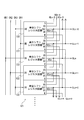
- FIG. 1 is a block diagram illustrating a configuration example (first embodiment) of a shift register circuit according to the present invention
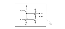
- 1 is a block diagram showing a configuration example (first embodiment) of a unit shift register circuit according to the present invention.
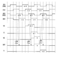
- FIG. 4 is an operation timing chart of the unit shift register circuit 122 (first embodiment) shown in FIG. 3.
- FIG. 6 is a first explanatory diagram for explaining an effect of the unit shift register circuit 122 (first embodiment) of the present invention. It is the 2nd explanatory view for explaining the effect of unit shift register circuit 122 (1st embodiment) of the present invention.
- FIG. 4 is an explanatory diagram for describing an operation example of a unit shift register circuit 122 (first embodiment) illustrated in FIG. 3.
- 5 is a chart in which voltage values are added to the operation timing chart of the unit shift register circuit 122 shown in FIG. 4.
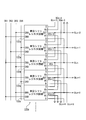
- FIG. 4 is a block diagram which shows the structural example (2nd Embodiment) of the shift register circuit by this invention.
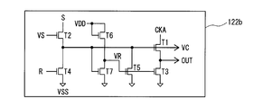
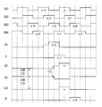
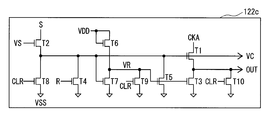
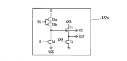
- 10 is a block diagram illustrating a configuration example (second embodiment) of the unit shift register circuit 122a illustrated in FIG. 9; 12 is an operation timing chart of the unit shift register circuit 122a (second embodiment) shown in FIG. It is a block diagram which shows the structural example (3rd Embodiment) of the unit shift register circuit 122b of this invention. 13 is an operation timing chart of the unit shift register circuit 122b (third embodiment) shown in FIG. It is a block diagram which shows the structural example (4th Embodiment) of the unit shift register circuit 122c of this invention. It is a block diagram which shows the structural example (5th Embodiment) of the unit shift register circuit 122d of this invention.
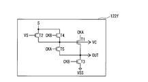
- FIG. 18 is a block diagram showing a configuration example (seventh embodiment) of a unit shift register circuit 122f shown in FIG. 19 is an operation timing chart of the unit shift register circuit 122f (seventh embodiment) illustrated in FIG. 18.
- FIG. 18 is a block diagram which shows the structural example (8th Embodiment) of the unit shift register circuit 122g of this invention.
- FIG. 9th Embodiment of the shift register circuit by this invention.
- 22 is a block diagram illustrating a configuration example (9th embodiment) of the pre-boost circuit 123 illustrated in FIG. 21. 22 is an operation timing chart of the shift register circuit 121h (9th embodiment) illustrated in FIG. 21. It is the characteristic view (description figure of 10th Embodiment) which showed an example of the characteristic of TFT which contains an oxide semiconductor in a semiconductor layer.
- the active matrix type liquid crystal display device 100 shown in FIG. 1 includes a plurality of signal lines SL1, SL2,..., SLm, a plurality of scanning lines GL1, GL2,. , SL2,..., SLm and a plurality of pixel portions PIX provided corresponding to the intersections of the plurality of scanning lines GL1, GL2,..., GLn (collectively referred to as GL). .
- These pixel portions PIX are arranged in a matrix to form the display area 110.
- Each pixel unit PIX has a thin film transistor (TFT) 114, which is a switching element in which a gate terminal is connected to a scanning line passing through a corresponding intersection and a source terminal is connected to a signal line passing through the intersection, and a video signal.
- TFT thin film transistor
- a pixel capacitor 115 having one end connected to the common substrate Tcom for holding is included.
- the liquid crystal display device 100 is provided with a signal line driving circuit 130 for driving the signal lines SL1, SL2,..., SLm and a scanning line driving circuit 120 for driving the scanning lines GL1, GL2,.
- the scanning line driving circuit 120 includes a shift register circuit 121, and the shift register circuit 121 generates a driving signal for each scanning line GL1, GL2,.
- FIG. 2 shows five unit shift register circuits 122 included in the shift register circuit 121 shown in FIG. 1 and their input / output signal lines.
- the shift register circuit 121 includes a plurality of stages (stages) connected in cascade (that is, multistage connection).
- the unit shift register circuit 122 constituting each stage includes a clock terminal CK, a set terminal S, a terminal VS connected to the gate electrode of the setting transistor, an output terminal OUT, a terminal VC connected to the node VC, and a reset terminal R. have.
- the signal name input / output to / from each terminal is the same as the terminal name, or the node name connected to each terminal is the same as the terminal name.
- the signal lines GLn-3, GLn-2, GLn-1, GLn, GLn + 1, GLn + 2, GLn + 3 and GLn + 4 connected to the output terminal OUT or the reset terminal R are a plurality of scanning lines GL shown in FIG. Corresponds to seven scanning lines arranged in succession. Further, subscripts such as “n-3” and “n” indicate “the number of stages” of the unit shift register circuit 122 that outputs the subscripts. In the example shown in FIG. 2, the central unit shift register circuit 122 has n stages, the upper two unit shift register circuits 122 have n-2 and n-1 stages in order from the top, and the lower two unit shift register circuits.
- 122 is an n + 1 stage and an n + 2 stage in order from the top.
- the n-2 stage and the n-1 stage are referred to as the preceding stage (or the preceding two stages) and the preceding stage, respectively, and the n + 1 stage and the n + 2 stage are respectively the next stage and the second stage. Called the stage.
- the n + 1 stage, the n + 2 stage, and the like are collectively referred to as the subsequent stage of the n stage.
- VCn-4, VCn-3, VCn-2, VCn-1, VCn, VCn + 1, VCn + 2, VCn + 3, and VCn + 4 are n-4, n-3, n-2, n-1, n, n + 1, respectively. , N + 2, n + 3, and n + 4 stage unit shift register circuit 122.
- the output GLn ⁇ 1 in the previous stage is input as the S signal that is an input signal of the terminal S in the Nth stage, and the signal VS as the input signal in the terminal VS in the Nth stage is input.
- the output VCn ⁇ 2 of two stages is input, and the output GLn + 2 of the second stage is input as an R signal that is an input signal of the terminal R of the Nth stage.
- the clock signal CK input to the terminal CK is a four-phase clock, and is connected in the order of CK1, CK2, CK3, CK4, CK1, CK2,.
- the unit shift register circuit 122 is a TFT T1 (hereinafter referred to as “transistor T1” or simply “T1”) connected to the GL (OUT) that drives each scanning line (for other TFTs). And T3, and transistors T2 and T4 connected to the node VC which is the gate electrode of T1.
- the gate terminal of T2 is connected to the signal VS, and the drain terminal is connected to the signal S.
- the transistors T1 to T4 are N-channel TFTs (thin film transistors).
- T1 is an output transistor for outputting a pulse signal to the output terminal OUT.
- T1 has a drain connected to the clock terminal CK, a gate connected to the node VC, and a source connected to the output terminal OUT.
- T1 performs an operation of boosting the output signal OUT by a bootstrap operation of boosting the gate voltage by a voltage charged in the parasitic capacitance between the source terminal and the gate electrode, which is not shown in FIG.
- T2 has a gate connected to the VS terminal, a drain connected to the set terminal S, and a source connected to the node VC.
- a voltage higher than the input signal of the set terminal S (for example, a sufficiently high voltage that can ensure the threshold voltage even when T2 deteriorates) is input to the VS terminal, and the input voltage of the set terminal S is supplied to the node VC as it is. it can.
- T3 has a gate connected to the R terminal, a drain connected to the output terminal OUT, and a source connected to the VSS terminal (that is, the power supply voltage VSS).
- T4 has a gate connected to the R terminal, a drain connected to the node VC, and a source connected to the VSS terminal.
- the power supply voltage VSS is a reference voltage in the operation of the unit shift register circuit 122.
- the transistor T1 is one of the configuration examples of the “output transistor”.
- the transistor T2 is one of the configuration examples of the “setting transistor”.
- the signal S input to the set terminal S corresponds to the “first input signal”, and the signal VS input to the terminal VS corresponds to the “second input signal”.
- FIG. 4 is a timing chart showing an operation example of the n-th unit shift register circuit 122.
- the four-phase clocks CK1 to CK4 are sequentially input to the unit shift register circuit 122 in each stage with a shift of a quarter cycle, and drive the unit shift register circuit 122.
- numbers “n ⁇ 6” to “n + 3” of the clock signals CK1 to CK4 indicate the number of stages of the unit shift register circuit 122 in which the pulse acts as a clock signal. That is, the number of unit shift register circuits 122 selected to output the output signal OUT by the clock signal CK is shown.
- the unit shift register circuit 122 in the previous stage operates, and the boosted node VCn-2 (the voltage thereof) is input to the VS terminal. .
- the unit shift register circuit 122 of the previous stage operates and the output node of GLn ⁇ 1 is input to the S terminal.
- VS is a boosted voltage
- the input signal from S is directly charged to the node VC.
- the CK pulse is output to the OUT terminal, that is, GLn.
- the output OUT is input to the R terminal two stages before, and pulls down the node VC of the unit shift register circuit 122 two stages before.
- the output GLn + 2 at the (N + 2) th stage is input to the R terminal, and the node VC and the node OUT are pulled down to VSS.
- FIG. 5A is a diagram showing the configuration of the unit shift register circuit 122 according to the present embodiment, in which a boost capacitor Cb that is a parasitic capacitance is clearly shown.
- FIG. 5B is a timing chart showing an operation example of the configuration shown in FIG. 5A. Note that FIG. 5B is the same as the timing chart of FIG.
- FIG. 5C is a configuration diagram showing a configuration example of the unit shift register circuit 222 by the diode connection method. In this case, the drain and gate of T2 are connected to the terminal S.
- FIG. 5D is a timing chart showing an operation example of the configuration shown in FIG. 5C.
- FIG. 6 is a characteristic diagram showing the relationship between the threshold voltage of the TFT and the amplitude voltage of the operable clock CK.
- the horizontal axis represents the threshold voltage of the TFT
- the vertical axis represents the operable clock amplitude voltage (lower limit value of the CK amplitude voltage).
- the relationship between the threshold voltage of the TFT and the lower limit value of the CK amplitude voltage can be approximated by a line segment.
- the operating condition is expressed using the threshold voltages of T1 and T2 as described above. Therefore, the lower limit value of the CK amplitude voltage that can be operated with respect to the threshold voltage of the TFT is 2 or more.
- the lower limit value of the CK amplitude voltage operable with respect to the threshold voltage of the TFT is reduced to a slope of 1. .
- the lower limit value of the CK amplitude voltage of this embodiment does not change much compared to the lower limit value of the CK amplitude voltage in the diode connection method.
- the operation margin for the threshold voltage shift is significantly improved as compared with the diode connection method.
- the above comparison is made by comparing the theoretical limit values, and it is assumed that the TFT of this embodiment and the diode connection method has a sufficient driving force. In other words, it does not take into account that it will not move due to lack of ability.
- FIG. 7 is a diagram in which voltage values are added to the block diagram shown in FIG.
- FIG. 8 is a chart in which voltage values are added to the operation timing chart of the unit shift register circuit 122 shown in FIG.
- CK H voltage (HIGH (H) level voltage) is + 10V
- CK L potential (LOW (L) level voltage) is -10V
- VSS is -10V
- the initial TFT threshold is 3V. It was.
- the voltage of the node VC is increased by the amplitude of CK by the bootstrap (here, the increase efficiency is 100%). That is, VC is boosted from 10V to 30V. Therefore, in the subsequent unit shift register circuit 122 to which the VC is input, 30 V is input to the gate and 10 V is input to the terminal S during the set operation (when the signal S is input to the terminal S).
- the node VC is precharged to 10 V without being affected by the threshold value of T2.
- Vgs is a gate-source voltage of T2
- Vds is a drain-source voltage.
- the shift register circuit 121a of the second embodiment differs from the shift register circuit 121 of the first embodiment shown in FIG. 2 in the configuration related to the clock signal CK.
- two types of clock signals CKA and CKB are input to the shift register circuit 121a.
- the shift register circuit 121 a has a configuration corresponding to the shift register circuit 121 illustrated in FIG. 1 in the liquid crystal display device 100 illustrated in FIG. 1, and the circuit around the scanning line GL is the same as that of the shift register circuit 121. It is.
- symbol and name are used in each embodiment.
- the shift register circuit 121a of the second embodiment includes a plurality of stages in which a plurality of unit shift register circuits 122a are connected in cascade.
- the previous-stage output GLn-1 is input to the N-stage S signal
- the previous-stage output VCn-2 is input to the N-stage VS signal
- two N-stage R signals are input to the N-stage R signal.
- the output GLn + 2 of the subsequent stage is input.
- the clock signal CK is a four-phase clock
- the clock signal CKA and the clock signal CKB are clock signals having opposite phases.
- the unit shift register circuit 122a includes T1 and T3 connected to GL (OUT) that drives each scanning line, and T2 and T2 connected to a node VC that is a gate electrode of T1. It consists of T4.
- the signal VS is connected to the gate terminal of T2, and the signal S is connected to the drain terminal.
- CKB having a phase opposite to that of CKA is connected to the gate terminal of T3.
- T3 acts as a TFT that pulls down the output terminal OUT (scanning line GL) by CKB having a phase opposite to that of CKA.
- FIG. 11 is a timing chart showing an operation example of the n-th unit shift register circuit 122a.
- CKA is CK1 and CKB is CK3
- the output terminal OUT is connected to the scanning line GLn.
- T3 which is a TFT for pulling down the scanning line GL
- the scanning line GL may be lifted by a leak current from the clock signal CK (CKA) to the output terminal OUT (GL).
- the noise of the scanning line GL can be suppressed by connecting the clock signal CKB to the gate of T3.
- the unit shift register circuit 122b of the third embodiment pulls down the output terminal OUT and the node VC compared to the unit shift register circuit 122a of the second embodiment shown in FIG.
- the configuration of this circuit is different.
- the configuration of the shift register circuit and the configuration of the liquid crystal display device when a plurality of unit shift register circuits 122b are used are the same as those in the first embodiment.
- the clock signal CKA is the same as the clock signal CK of the first embodiment.
- the pull-down circuit includes T3, T5, T6, and T7.
- the drain and gate of T6 are connected to the VDD power source, and the source is connected to the drain of T7 and the gates of T5 and T3 (ie, node VR).
- T7 has a source connected to the VSS power supply and a gate connected to the node VC.
- T5 has a drain connected to the node VC and a source connected to the VSS power supply.
- T3 has a drain connected to the output terminal OUT and a source connected to the VSS power source.
- T6 and T7 are circuits that generate a VR signal.
- T1 output OUT
- the voltage is lowered to the voltage of the threshold voltage of T6 from the potential of the VDD power supply via T6.
- the node VC and the output node OUT are always pulled down to the VSS level by T3 and T5 to which the node VR is precharged and the node VR is connected.
- T7 is turned ON to lower the node VR to near the VSS level (timing (1) in FIG. 13).
- the VR potential at this time is determined by the ratio of T6 and T7, and can be realized by increasing the capability of T7 with respect to T6.
- noise resistance can be improved by eliminating the period in which the node VC and the node GL are floating when not selected.
- the node VC can be completely prevented from being lifted by the coupling due to the CKA pulse, the clock noise at which the CKA noise is output to the GL can be suppressed.
- the gate voltage of T7 since a voltage drop due to the threshold voltage of the precharge voltage level during the set operation can be avoided, the gate voltage of T7 does not need to be large in consideration of the voltage drop after deterioration.
- the size can be reduced.
- the circuit area can be reduced accordingly.
- the unit shift register circuit 122c of the fourth embodiment pulls down the output terminal OUT and the node VC compared to the unit shift register circuit 122b of the third embodiment shown in FIG.
- the configuration of this circuit is different.
- the configuration of the shift register circuit and the configuration of the liquid crystal display device when a plurality of unit shift register circuits 122c are used are the same as those in the first embodiment.
- the clock signal CKA is the same as the clock signal CK of the first embodiment.
- the unit shift register circuit 122c of the fourth embodiment adds a CLR signal (clear signal) to the pull-down circuit of the third embodiment, and the CLR signal is input to the gate T8.
- T9, and T10 are connected to node VC, node VR, and node OUT, respectively.
- the drain of T8 is connected to the node VC
- the drain of T9 is connected to the node VR
- the drain of T10 is connected to the node OUT
- the source is connected to the VSS power supply.
- This CLR signal is input from outside the unit shift register circuit 122c.
- a shift register circuit When a shift register circuit is configured by using a plurality of unit shift register circuits 122c according to the fourth embodiment, all stages of the shift register circuit can be initialized collectively. For example, by clearing at the beginning of the scanning period, it is possible to operate from an initialized state, and unexpected operations and outputs can be suppressed. Further, by clearing at the end of the scanning period, the circuit is initialized and the charge is removed. Therefore, it is possible to prevent the TFT from being deteriorated due to the remaining charge when the operation is stopped.
- the unit shift register circuit 122d of the fifth embodiment is different from the unit shift register circuit 122c of the fourth embodiment shown in FIG. 14 between the node VC and the node OUT (GL).
- the difference is that a capacitive element Cb1 is provided between the gate electrode and the source terminal of T1.
- the configuration of the shift register circuit and the configuration of the liquid crystal display device when a plurality of unit shift register circuits 122d are used are the same as those in the first embodiment.
- the clock signal CKA is the same as the clock signal CK of the first embodiment.
- Capacitance Cb1 works as a push-up capacity during bootstrap operation. Therefore, the pushing-up efficiency is increased and the driving force can be improved. Further, during the non-selection operation, it works to stabilize the potential of the node VC (that is, to prevent oscillation), and it is possible to prevent the node VC from being lifted by coupling with the CKA pulse.
- the unit shift register circuit 122e of the sixth embodiment is different in the configuration of the setting transistor T2 from the unit shift register circuit 122a of the second embodiment shown in FIG. .
- the configuration of the shift register circuit and the configuration of the liquid crystal display device when a plurality of unit shift register circuits 122e are used are the same as those in the second embodiment.
- the unit shift register circuit 122e of the sixth embodiment is characterized in that it has a dual configuration including a plurality of transistors in which the setting transistor T2 in the second embodiment is cascode-connected. That is, in the unit shift register circuit 122e of the sixth embodiment, the setting transistors are cascode-connected, that is, in this case, the gates of each other are connected and the drain of one transistor and the source of the other transistor are connected. A plurality of transistors T2a and T2b.
- the signal VS is input to the gates of T2a and T2b, the signal S is input to the drain of T2a, and the source of T2b is connected to the node VC.
- the set TFT By making the set TFT dual, during operation, when the node VC is boosted by bootstrap, the potential difference applied between the VDS of the set TFT can be halved, and the breakdown voltage can be improved. Although the driving force is reduced by adopting the dual configuration, the VS potential during the precharge operation is very large, so that a sufficient driving force can be obtained.
- the shift register circuit 121f of the seventh embodiment differs from the shift register circuit 121a of the second embodiment shown in FIG. 9 in that the reset terminal R is omitted. Yes.
- the connection relationship of the shift register circuit 121f in the liquid crystal display device is the same as in the second embodiment.
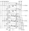
- the shift register circuit 121f of the seventh embodiment is composed of a plurality of stages in which a plurality of unit shift register circuits 122f are connected in cascade.
- the preceding stage output GLn ⁇ 1 is input to the Nth stage S signal, and the preceding stage output VCn ⁇ 2 is input to the Nth stage VS signal.
- CK is a four-phase clock
- CKB CK1
- the unit shift register circuit 122f includes T1 and T3 connected to GL (OUT) that drives each scanning line, T2 and T4 connected to the node VC that is a gate electrode of T1, and nodes VC and OUT. It consists of T5 connected.
- the gate terminal of T2 is connected to the signal VS, and the drain terminal is connected to the signal S.
- the gate terminal of T3 connects CKB having the opposite phase to CKA.
- the gate terminal of T4 is connected to CKB, and the drain terminal is connected to signal S.
- CKA is connected to the gate terminal of T5.
- the node VC is pulled down by the reset TFT T4.
- the node VC is reset by T4 and T5.
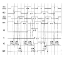
- FIG. 19 is a timing chart showing an operation example of the nth unit shift register circuit 122f.
- CKA is CK1 and CKB is CK3
- the output terminal OUT is connected to the scanning line GLn.
- T4 connects the drain and the source to the S terminal and the node VC, respectively, and shorts the node VC with the S terminal by the CKB signal.
- T5 connects the drain and source to the node VC and the output OUT node, respectively, and shorts the node VC to the OUT terminal by the CKA signal.
- T3 pulls down the OUT terminal by the CKB signal.
- the node VC is short-circuited with the OUT node by turning on T5. Since the OUT node is loaded with a larger GL than the node VC, the coupling capacitance between the CKA and the node VC is reduced, so that noise at the node VC can be suppressed.
- T4 is turned ON to connect the node VC to the S terminal.
- the node VC is connected to the GL of the previous unit shift register circuit 122f, the potential is fixed.
- pull-down can be performed with a smaller number of elements than in the pull-down circuit of the third embodiment.
- the unit shift register circuit 122g of the eighth embodiment differs from the unit shift register circuit 122f of the seventh embodiment shown in FIG. 18 in the configuration of the pull-down circuit.
- the configuration of the shift register circuit and the configuration of the liquid crystal display device when a plurality of unit shift register circuits 122f are used are the same as those in the seventh embodiment.
- the unit shift register circuit 122g of the eighth embodiment adds a CLR signal in addition to the configuration of the shift register 122f of the seventh embodiment shown in FIG. 18, and the CLR signal is input to the gate.
- T6 and T7 connected to the node VC and the node OUT, respectively.
- a shift register circuit When a shift register circuit is configured by using a plurality of unit shift register circuits 122g according to the eighth embodiment, all stages of the shift register circuit can be initialized collectively. For example, by clearing at the beginning of the scanning period, it is possible to operate from an initialized state, and unexpected operations and outputs can be suppressed. Further, by clearing at the end of the scanning period, the circuit is initialized and the charge is removed. Therefore, it is possible to prevent the TFT from being deteriorated due to the remaining charge when the operation is stopped.
- the shift register circuit 121h of the ninth embodiment shown in FIG. 21 has a configuration corresponding to the shift register circuit 121 shown in FIG. 1 in the liquid crystal display device 100 shown in FIG. This is the same as the shift register circuit 121.
- the shift register circuit 121h shown in FIG. 21 includes a plurality of stages in which two pre-boost circuits 123 and a plurality of unit shift register circuits 122c shown in FIG. 14 are connected in cascade.
- the output GLn-1 of the previous stage is input to the S signal of the Nth stage
- the output VCn-2 of the previous stage is input to the VS signal of the Nth stage
- N The second stage output GLn + 2 is input to the stage R signal.
- the CK signal is a four-phase clock and is connected in the order of CK1, CK2, CK3, and CK4 for every four stages of the unit shift register circuit 122c.
- Each pre-boost circuit 123 is provided with an S1 terminal, an S2 terminal, a DVC terminal, a CK terminal, and a CLR terminal.
- the signal SP1 is input to the S1 input
- the signal SP2 is input to the S2 input.
- the node DVC (signal DVC1) of the first stage pre-boost circuit 123 is connected to the VS input of the first stage unit shift register circuit 122c.
- the node DVC (signal DVC2) of the second stage pre-boost circuit 123 is connected to the VS input of the second stage unit shift register circuit 122c.
- the DVC signals boosted by the two-stage pre-boost circuit 123 are sequentially input to the VS terminal of the first two-stage unit shift register circuit 122c.
- the signal SP2 is connected to the S input of the first stage unit shift register circuit 122c.
- the signals SP1 and SP2 are pulse signals generated at the start of the operation of the shift register circuit 121h.
- the unit shift register circuit 122c is composed of the same circuit as that of the fourth embodiment shown in FIG.
- the pre-boost circuit 123 is a pre-boost circuit for generating VS signals input to the first and second stages of the unit shift register circuit 122c. As shown in FIG. 22, in the preboost circuit 123, the S1 terminal is diode-connected to the drain and gate of T21, and the value obtained by dropping the threshold voltage of T21 with respect to the voltage input to S1 is a node from the source. Operates to set to DVC. T22 is a TFT for initialization. The CLR signal is connected to the gate, the drain is connected to the node DVC, the source is connected to the VSS power supply, and the node DVC is reset to the VSS level when the CLR signal is H.
- CK is input to the gate, the drain is connected to the node DVC, the source is connected to the VSS power supply, the CK signal is H, and the node DVC is reset to the VSS level.
- the capacitor Cp is a capacitive element for boosting the node DVC. One end of the capacitor Cp is connected to the node DVC, and the other end is connected to the terminal SP2.
- DVC1 and DVC2 are boosted for the amplitude of SP2 because the signal SP2 rises and is connected to the boosting capacitor Cp of the pre-boost circuit 123.
- the first stage unit shift register circuit 122c for driving the scanning line GL1 has SP2 connected to the S terminal and DVC1 connected to the VS terminal. ), The node VC1 is precharged to the potential of SP2 connected to the S terminal.
- GL1 is connected to the S terminal and DVC2 is connected to the VS terminal of the second stage unit shift register circuit 122c for driving the scanning line GL2. ), The node VC2 is precharged to the potential of GL1 connected to the S terminal.
- the scanning line GL rises sequentially.
- the pre-boost circuit 123 can perform precharge from the first stage set signal without the influence of the threshold value, a sufficient operation margin can be obtained.
- the tenth embodiment is characterized by the material of the semiconductor layer of the TFT in the unit shift register circuits 121a to 121g and the preboost circuit 123 described above. That is, the TFT used in each of the above embodiments can include an oxide semiconductor in the semiconductor layer.
- the oxide semiconductor layer is, for example, an In—Ga—Zn—O-based semiconductor layer.
- the oxide semiconductor layer includes, for example, an In—Ga—Zn—O-based semiconductor.
- an In—Ga—Zn—O-based semiconductor film containing In, Ga, and Zn at a ratio of 1: 1: 1 is used.
- a TFT having an In—Ga—Zn—O-based semiconductor layer has high mobility (more than 20 times that of an a-Si TFT) and low leakage current (less than one hundredth of that of an a-Si TFT). It is suitably used as a drive TFT and a pixel TFT.
- a TFT having an In—Ga—Zn—O-based semiconductor layer is used, power consumption of the display device can be significantly reduced (see FIG. 24).
- FIG. 24 is a characteristic diagram showing the correspondence between the gate voltage and the drain-source current.
- the In—Ga—Zn—O-based semiconductor may be amorphous, may include a crystalline portion, and may have crystallinity.
- a crystalline In—Ga—Zn—O-based semiconductor in which the c-axis is oriented substantially perpendicular to the layer surface is preferable.
- Such a crystal structure of an In—Ga—Zn—O-based semiconductor is disclosed in, for example, Japanese Patent Laid-Open No. 2012-134475. For reference, the entire disclosure of Japanese Patent Application Laid-Open No. 2012-134475 is incorporated herein by reference.
- the oxide semiconductor layer may include another oxide semiconductor instead of the In—Ga—Zn—O-based semiconductor.
- Zn—O based semiconductor ZnO
- In—Zn—O based semiconductor IZO (registered trademark)
- Zn—Ti—O based semiconductor ZTO
- Cd—Ge—O based semiconductor Cd—Pb—O based
- CdO cadmium oxide
- Mg—Zn—O based semiconductor Mg—Zn—O based semiconductor
- In—Sn—Zn—O based semiconductor eg In 2 O 3 —SnO 2 —ZnO
- In—Ga—Sn—O based semiconductor etc.
- different S inputs (first input signals) and VS are applied to the source terminal (second source terminal) and the gate terminal (second gate electrode) of the setting transistor T2.
- an input second input signal (where the voltage of the first input signal ⁇ the voltage of the second input signal)
- the gate terminal (first gate electrode) of the output transistor T1 is charged (that is, precharged).
- the diode-connected TFT and the second bootstrap capacitor can be easily omitted.
- the VS input (second input signal) for example, a signal of the gate (first gate electrode) of the output transistor T1 of another unit shift register circuit can be used, so that it can be easily prepared. Therefore, according to the unit shift register circuit of the present invention, the influence due to the characteristic deterioration can be easily reduced with a small number of circuit elements.
- the embodiment of the present invention is not limited to the above.
- changes that combine the configurations of the above-described embodiments or omit a part of the configuration in each of the above-described embodiments can be made as appropriate.
- the present invention can be applied to a unit shift register circuit that can reduce the influence of characteristic deterioration with a small number of circuit elements.
- liquid crystal display device 110 display area 120 scanning line driving circuit 121, 121a, 121f, 121h shift register circuit 130 signal line driving circuit PIX pixel GL1 to GLn scanning line 122, 122a to 122g unit shift register circuit T1 to T10 TFT Cb1 capacitance element
Landscapes
- Engineering & Computer Science (AREA)
- Physics & Mathematics (AREA)
- Computer Hardware Design (AREA)
- General Physics & Mathematics (AREA)
- Theoretical Computer Science (AREA)
- Chemical & Material Sciences (AREA)
- Crystallography & Structural Chemistry (AREA)
- Liquid Crystal Display Device Control (AREA)
- Shift Register Type Memory (AREA)
- Control Of Indicators Other Than Cathode Ray Tubes (AREA)
- Liquid Crystal (AREA)
Abstract
Description
本願は、2013年6月28日に、日本に出願された特願2013-136485号に基づき優先権を主張し、その内容をここに援用する。
ダイオード接続のTFTを用いた場合、プリチャージ電圧はTFTの閾値電圧分降下した値となる。a-Siや酸化インジウムガリウム亜鉛等の酸化物半導体を用いたTFTは、ゲート電極に印加される電圧ストレスにより、閾値電圧が変動する特性をもつため、時間経過に従って特性劣化が進み、プリチャージ電圧はその分低下する。プリチャージ電圧が低下していくと、ブートストラップにより昇圧される電圧も低下し、出力用TFTの駆動力が低下し、出力波形がなまったり、さらに劣化がすすむと、出力電圧が低下して、シフトレジスタ動作が不安定となる。この問題は例えば特性劣化を考慮して大きなサイズのTFTを使用すれば解決することができる。ただし、この場合、回路面積が大きくなってしまうという課題が残る。
特許文献1に記載されている単位シフトレジスタ回路では、2つのブートストラップコンデンサの使用により、回路は閾値電圧のレベル又は変動に敏感ではなくなるので、アモルファスシリコン技術による実施が可能となる。
まず、図1を用いて本発明の実施形態に係る液晶表示装置の構成例を説明する。図1に示すアクティブマトリクス型の液晶表示装置100には、複数本の信号線SL1、SL2、…、SLmと、複数本の走査線GL1、GL2、…、GLnと、それら複数本の信号線SL1、SL2、…、SLmと複数本の走査線GL1、GL2、…、GLn(総称する場合GLとする)との交差点にそれぞれ対応して設けられた複数個の画素部PIXとが含まれている。これらの画素部PIXはマトリクス状に配置されて表示領域110を構成する。各画素部PIXは、対応する交差点を通過する走査線にゲート端子が接続されるとともに、交差点を通過する信号線にソース端子が接続されたスイッチング素子である薄膜トランジスタ(TFT)114や、映像信号を保持するための共通基板Tcomに一端が接続された画素容量115などを含む。また、液晶表示装置100には信号線SL1、SL2、…、SLmを駆動する信号線駆動回路130と走査線GL1、GL2、…、GLnを駆動する走査線駆動回路120とが設けられている。この走査線駆動回路120は、シフトレジスタ回路121を備え、そしてシフトレジスタ回路121は、各走査線GL1、GL2、…、GLnの駆動信号を生成する。
そのため、ダイオード接続を挿入しなくても他の段への逆流が発生することなく、充電されたゲート電極の電圧低下を防止することができる。
図6において、横軸はTFTの閾値電圧を示し、縦軸は動作可能なクロックの振幅電圧(CK振幅電圧の下限値)を示す。TFTの閾値電圧とCK振幅電圧の下限値との関係は、線分で近似することができる。
ダイオード接続方式では、上述のように動作条件がT1及びT2の閾値電圧を用いて表されるため、TFTの閾値電圧に対して動作可能なCK振幅電圧の下限値は、傾き2以上となる。一方、本実施形態では、上述のように動作条件がT1の閾値電圧を用いて表されるため、TFTの閾値電圧に対して動作可能なCK振幅電圧の下限値は、傾き1まで削減される。
ただし、上記の比較は、理論限界値を比較したものであり、本実施形態とダイオード接続方式でのTFTは十分な駆動力があるものとする。すなわち、能力不足で動かなくなるということは考慮していない。
次に、図9から図11を参照して、本発明の第2実施形態について説明する。図9に示したように、第2実施形態のシフトレジスタ回路121aは、図2に示した第1実施形態のシフトレジスタ回路121と比較して、クロック信号CKに係る構成が異なっている。
本実施形態では、シフトレジスタ回路121aには、2種類のクロック信号CKAとCKBとが入力される。なお、シフトレジスタ回路121aは、図1に示した液晶表示装置100内で図1に示したシフトレジスタ回路121に対応する構成であり、走査線GL周辺の回路はシフトレジスタ回路121の場合と同一である。なお、信号及び端子名については各実施形態で同一符号や名称を用いている。
次に、図12及び図13を参照して、本発明の第3実施形態について説明する。図12に示したように、第3実施形態の単位シフトレジスタ回路122bは、図10に示した第2実施形態の単位シフトレジスタ回路122aと比較して、出力端子OUT及びノードVCをプルダウンするための回路(プルダウン回路)の構成が異なっている。単位シフトレジスタ回路122bを複数用いた場合のシフトレジスタ回路の構成や液晶表示装置の構成は第1実施形態と同様である。クロック信号CKAは第1実施形態のクロック信号CKと同じである。
次に、図14を参照して、本発明の第4実施形態について説明する。図14に示したように、第4実施形態の単位シフトレジスタ回路122cは、図12に示した第3実施形態の単位シフトレジスタ回路122bと比較して、出力端子OUT及びノードVCをプルダウンするための回路(プルダウン回路)の構成が異なっている。単位シフトレジスタ回路122cを複数用いた場合のシフトレジスタ回路の構成や液晶表示装置の構成は第1実施形態と同様である。クロック信号CKAは第1実施形態のクロック信号CKと同じである。
次に、図15を参照して、本発明の第5実施形態について説明する。図15に示したように、第5実施形態の単位シフトレジスタ回路122dは、図14に示した第4実施形態の単位シフトレジスタ回路122cと比較して、ノードVCとノードOUT(GL)との間、すなわちT1のゲート電極とソース端子間に、容量素子Cb1を設けた点が異なっている。単位シフトレジスタ回路122dを複数用いた場合のシフトレジスタ回路の構成や液晶表示装置の構成は第1実施形態と同様である。クロック信号CKAは第1実施形態のクロック信号CKと同じである。
次に、図16を参照して、本発明の第6実施形態について説明する。図16に示したように、第6実施形態の単位シフトレジスタ回路122eは、図10に示した第2実施形態の単位シフトレジスタ回路122aと比較して、セット用トランジスタT2の構成が異なっている。単位シフトレジスタ回路122eを複数用いた場合のシフトレジスタ回路の構成や液晶表示装置の構成は第2実施形態と同様である。
次に、図17から図19を参照して、本発明の第7実施形態について説明する。図17に示したように、第7実施形態のシフトレジスタ回路121fは、図9に示した第2実施形態のシフトレジスタ回路121aと比較して、リセット端子Rが省略されている点が異なっている。シフトレジスタ回路121fの液晶表示装置内の接続関係は第2実施形態と同様である。
次に、図20を参照して、本発明の第8実施形態について説明する。図20に示したように、第8実施形態の単位シフトレジスタ回路122gは、図18に示した第7実施形態の単位シフトレジスタ回路122fと比較して、プルダウン回路の構成が異なっている。
単位シフトレジスタ回路122fを複数用いた場合のシフトレジスタ回路の構成や液晶表示装置の構成は第7実施形態と同様である。
次に、図21から図23を参照して、本発明の第9実施形態について説明する。図21に示した第9実施形態のシフトレジスタ回路121hは、図1に示した液晶表示装置100内では図1に示したシフトレジスタ回路121に対応する構成であり、走査線GL周辺の回路はシフトレジスタ回路121の場合と同一である。
第10実施形態は、上述した単位シフトレジスタ回路121a~121gやプリブースト回路123内のTFTの半導体層の材料に特徴を有する。すなわち、上記各実施形態で用いるTFTは、半導体層に酸化物半導体を含むものとすることができる。
Claims (19)
- シフトレジスタ回路の各段を構成する単位シフトレジスタ回路であって、
第1ゲート電極、第1ソース端子及び第1ドレイン端子を有し、所定のクロック信号を前記第1ドレイン端子に入力し、前記第1ソース端子から出力信号を出力する出力用トランジスタと、
第2ゲート電極、第2ソース端子及び第2ドレイン端子を有し、前記出力用トランジスタの前記第1ゲート電極に前記第2ソース端子が接続されたトランジスタであって、第1入力信号を前記第2ドレイン端子に入力し、前記出力用トランジスタの前記第1ゲート電極を充電する際に前記第1入力信号の電圧より高い電圧となる第2入力信号を前記第2ゲート電極に入力するセット用トランジスタと
を備える単位シフトレジスタ回路。 - 前記セット用トランジスタが前記出力用トランジスタの前記第1ゲート電極を充電する際に、前記第1入力信号および前記第2入力信号が立ち上がり、前記第1ゲート電極を充電後、前記第1入力信号の電圧の立ち下がりより先に前記第2入力信号の電圧が立ち下がる請求項1に記載の単位シフトレジスタ回路。
- 前記出力用トランジスタが、前記第1ソース端子と前記第1ゲート電極間の寄生容量に充電された電圧によって前記第1ゲート電圧を昇圧するブートストラップ動作により前記出力信号を昇圧する請求項1又は2に記載の単位シフトレジスタ回路。
- 前記第1入力信号が他の段の前記単位シフトレジスト回路の出力信号であり、
前記第2入力信号が他の段の前記単位シフトレジスト回路の出力用トランジスタの前記第1ゲート電極の信号である請求項1から3のいずれか1項に記載の単位シフトレジスタ回路。 - 前記クロック信号が重なりのある多相クロック信号であって、複数の前記単位シフトレジスタ回路に対して異なる複数相のクロック信号が供給される請求項4項に記載の単位シフトレジスタ回路。
- 前記出力用トランジスタの前記第1ゲート電極が、後段の前記単位シフトレジスト回路の出力信号に応じてリセットされる請求項1から5のいずれか1項に記載の単位シフトレジスタ回路。
- 前記出力用トランジスタの前記第1ゲート電極を前記クロック信号に応じてリセットするリセット回路を備える請求項1から5のいずれか1項に記載の単位シフトレジスタ回路。
- 前記単位シフトレジスタ回路の出力信号を前記クロック信号に応じてプルダウンするプルダウン回路を備える請求項1から7のいずれか1項に記載の単位シフトレジスタ回路。
- 前記単位シフトレジスタ回路の出力信号と前記出力用トランジスタの前記第1ゲート電極とを該第1ゲート電極の電圧に応じてプルダウンするプルダウン回路を備える請求項1から7のいずれか1項に記載の単位シフトレジスタ回路。
- 前記単位シフトレジスタ回路の出力信号と前記出力用トランジスタの前記第1ゲート電極とを所定のクリア信号に応じてプルダウンするプルダウン回路を備える請求項1から9のいずれか1項に記載の単位シフトレジスタ回路。
- 前記出力用トランジスタの前記第1ゲート電極と前記第1ソース端子との間に接続された容量素子を備える請求項1から10のいずれか1項に記載の単位シフトレジスタ回路。
- 前記セット用トランジスタが、カスコード接続した複数のトランジスタから構成されている請求項1から11のいずれか1項に記載の単位シフトレジスタ回路。
- 少なくとも前記出力用トランジスタ及び前記セット用トランジスタが、半導体層に酸化物半導体を含む請求項1から12のいずれか1項に記載の単位シフトレジスタ回路。
- 前記酸化物半導体が、酸化インジウムガリウム亜鉛(In-Ga-Zn-O系半導体;インジウム(In)、ガリウム(Ga)、亜鉛(Zn)及び酸素(O)を含む酸化物半導体)である請求項13に記載の単位シフトレジスタ回路。
- 前記酸化物半導体が、結晶性を有する請求項14に記載の単位シフトレジスタ回路。
- 請求項1から15のいずれか1項に記載の単位シフトレジスタ回路を多段接続したシフトレジスタ回路であって、
N-1段目の前記単位シフトレジスタ回路の出力信号を、N段目の前記単位シフトレジスタ回路の前記第1入力信号力とし、
N-2段目の前記単位シフトレジスタ回路の出力用トランジスタの前記第1ゲート電極の信号を、N段目の前記単位シフトレジスタ回路の前記第2入力信号とするシフトレジスタ回路。 - 各段の前記単位シフトレジスタ回路に対し、前記クロック信号として、4相クロック信号が4分の1周期ずつ周期をずらして順に入力される請求項16に記載のシフトレジスタ回路。
- シフトレジスタ回路の各段を構成する単位シフトレジスタ回路の制御方法であって、
前記単位シフトレジスタ回路が、
第1ゲート電極、第1ソース端子及び第1ドレイン端子を有し、所定のクロック信号を前記第1ドレイン端子に入力し、前記第1ソース端子から出力信号を出力する出力用トランジスタと、
第2ゲート電極、第2ソース端子及び第2ドレイン端子を有し、前記出力用トランジスタの前記第1ゲート電極に前記第2ソース端子が接続されたトランジスタであって、第1入力信号を前記第2ドレイン端子に入力し、前記第1入力信号と異なる第2入力信号を前記第2ゲート電極に入力するセット用トランジスタと
を備え、
前記出力用トランジスタの前記第1ゲート電極を充電する際に、前記セット用トランジスタに対し、前記第1入力信号の電圧より高い電圧の第2入力信号を入力する単位シフトレジスタ回路の制御方法。 - 複数の画素と、
前記複数の画素が接続された複数の走査線と、
シフトレジスタ回路の各段を構成する単位シフトレジスタ回路であって、
第1ゲート電極、第1ソース端子及び第1ドレイン端子を有し、所定のクロック信号を前記第1ドレイン端子に入力し、前記第1ソース端子から前記各走査線を駆動する出力信号を出力する出力用トランジスタと、
第2ゲート電極、第2ソース端子及び第2ドレイン端子を有し、前記出力用トランジスタの前記第1ゲート電極に前記第2ソース端子が接続されたトランジスタであって、第1入力信号を前記第2ドレイン端子に入力し、前記出力用トランジスタの前記第1ゲート電極を充電する際に前記第1入力信号の電圧より高い電圧となる第2入力信号を前記第2ゲート電極に入力するセット用トランジスタと
をそれぞれが備える複数の単位シフトレジスタ回路と
を備える表示装置。
Priority Applications (3)
| Application Number | Priority Date | Filing Date | Title |
|---|---|---|---|
| JP2015523876A JPWO2014208123A1 (ja) | 2013-06-28 | 2014-02-25 | 単位シフトレジスタ回路、シフトレジスタ回路、単位シフトレジスタ回路の制御方法及び表示装置 |
| CN201480036204.9A CN105340021B (zh) | 2013-06-28 | 2014-02-25 | 单位移位寄存器电路、移位寄存器电路、单位移位寄存器电路的控制方法和显示装置 |
| US14/901,461 US10068543B2 (en) | 2013-06-28 | 2014-02-25 | Unit shift register circuit, shift register circuit, method for controlling unit shift register circuit, and display device |
Applications Claiming Priority (2)
| Application Number | Priority Date | Filing Date | Title |
|---|---|---|---|
| JP2013-136485 | 2013-06-28 | ||
| JP2013136485 | 2013-06-28 |
Publications (1)
| Publication Number | Publication Date |
|---|---|
| WO2014208123A1 true WO2014208123A1 (ja) | 2014-12-31 |
Family
ID=52141480
Family Applications (1)
| Application Number | Title | Priority Date | Filing Date |
|---|---|---|---|
| PCT/JP2014/054517 Ceased WO2014208123A1 (ja) | 2013-06-28 | 2014-02-25 | 単位シフトレジスタ回路、シフトレジスタ回路、単位シフトレジスタ回路の制御方法及び表示装置 |
Country Status (4)
| Country | Link |
|---|---|
| US (1) | US10068543B2 (ja) |
| JP (2) | JPWO2014208123A1 (ja) |
| CN (1) | CN105340021B (ja) |
| WO (1) | WO2014208123A1 (ja) |
Cited By (8)
| Publication number | Priority date | Publication date | Assignee | Title |
|---|---|---|---|---|
| JP2016029797A (ja) * | 2014-07-24 | 2016-03-03 | 株式会社半導体エネルギー研究所 | 半導体装置、表示モジュール及び電子機器 |
| WO2016136528A1 (ja) * | 2015-02-23 | 2016-09-01 | シャープ株式会社 | シフトレジスタ回路およびそれを備えた表示装置 |
| JPWO2014148171A1 (ja) * | 2013-03-21 | 2017-02-16 | シャープ株式会社 | シフトレジスタ |
| JPWO2015190488A1 (ja) * | 2014-06-13 | 2017-06-01 | シャープ株式会社 | シフトレジスタ回路、及びそれを備えた表示装置 |
| US20170186377A1 (en) * | 2015-12-29 | 2017-06-29 | Samsung Display Co., Ltd. | Gate driver and display device including the same |
| JP2019174595A (ja) * | 2018-03-28 | 2019-10-10 | シャープ株式会社 | アクティブマトリクス基板および表示装置 |
| JP2019174596A (ja) * | 2018-03-28 | 2019-10-10 | シャープ株式会社 | アクティブマトリクス基板および表示装置 |
| JP2019537073A (ja) * | 2016-10-18 | 2019-12-19 | 深▲セン▼市華星光電技術有限公司 | Goa駆動回路及び液晶表示装置 |
Families Citing this family (15)
| Publication number | Priority date | Publication date | Assignee | Title |
|---|---|---|---|---|
| US8736315B2 (en) * | 2011-09-30 | 2014-05-27 | Semiconductor Energy Laboratory Co., Ltd. | Semiconductor device |
| TWI611413B (zh) * | 2016-12-30 | 2018-01-11 | 友達光電股份有限公司 | 移位暫存器電路 |
| US11145268B2 (en) * | 2017-04-10 | 2021-10-12 | Sharp Kabushiki Kaisha | Active matrix substrate including setting thin film transistor and resetting thin film transistor and display device including same |
| CN106952602B (zh) * | 2017-04-14 | 2022-01-21 | 京东方科技集团股份有限公司 | 反相器模块、移位寄存器单元、阵列基板及显示装置 |
| US10923064B2 (en) * | 2017-04-17 | 2021-02-16 | Sharp Kabushiki Kaisha | Scanning signal line drive circuit and display device equipped with same |
| CN107342049B (zh) * | 2017-08-30 | 2019-10-01 | 上海天马有机发光显示技术有限公司 | 显示面板和显示面板的驱动方法 |
| CN109655877B (zh) * | 2019-01-04 | 2020-12-01 | 京东方科技集团股份有限公司 | 平板探测器的像素结构、平板探测器及摄像系统 |
| JP7412360B2 (ja) * | 2019-02-05 | 2024-01-12 | 株式会社半導体エネルギー研究所 | 表示装置および電子機器 |
| US11138947B2 (en) * | 2019-06-12 | 2021-10-05 | Sharp Kabushiki Kaisha | Scanning signal line drive circuit and display device provided with same |
| US11314136B2 (en) * | 2019-06-28 | 2022-04-26 | Sharp Kabushiki Kaisha | Active matrix substrate and display device |
| US11475968B2 (en) * | 2020-02-27 | 2022-10-18 | Sharp Kabushiki Kaisha | Shift register circuit, active matrix substrate, and display apparatus |
| CN115715411A (zh) * | 2021-05-31 | 2023-02-24 | 京东方科技集团股份有限公司 | 移位寄存器单元及其驱动方法、栅极驱动电路和显示装置 |
| KR102641231B1 (ko) * | 2021-10-06 | 2024-02-29 | 호서대학교 산학협력단 | 스캔 구동 회로 |
| CN119487565A (zh) * | 2023-05-19 | 2025-02-18 | 京东方科技集团股份有限公司 | 显示基板以及显示装置 |
| JP2025077259A (ja) * | 2023-11-06 | 2025-05-19 | シャープディスプレイテクノロジー株式会社 | 表示装置 |
Citations (6)
| Publication number | Priority date | Publication date | Assignee | Title |
|---|---|---|---|---|
| JP2003101406A (ja) * | 2001-09-20 | 2003-04-04 | Matsushita Electric Ind Co Ltd | 信号伝送回路、固体撮像装置、カメラおよび液晶表示装置 |
| JP2003242797A (ja) * | 2002-02-18 | 2003-08-29 | Matsushita Electric Ind Co Ltd | 信号伝送回路 |
| JP2003249848A (ja) * | 2002-02-26 | 2003-09-05 | Matsushita Electric Ind Co Ltd | 信号伝送回路の駆動方法 |
| JP2010250303A (ja) * | 2009-03-27 | 2010-11-04 | Semiconductor Energy Lab Co Ltd | 液晶表示装置 |
| JP2011070761A (ja) * | 2009-09-25 | 2011-04-07 | Beijing Boe Optoelectronics Technology Co Ltd | シフト・レジスタおよびゲートライン駆動装置 |
| JP2011199851A (ja) * | 2010-02-23 | 2011-10-06 | Semiconductor Energy Lab Co Ltd | 半導体装置及び表示装置 |
Family Cites Families (26)
| Publication number | Priority date | Publication date | Assignee | Title |
|---|---|---|---|---|
| FR2524714B1 (fr) * | 1982-04-01 | 1986-05-02 | Suwa Seikosha Kk | Transistor a couche mince |
| TW525139B (en) * | 2001-02-13 | 2003-03-21 | Samsung Electronics Co Ltd | Shift register, liquid crystal display using the same and method for driving gate line and data line blocks thereof |
| US7486269B2 (en) * | 2003-07-09 | 2009-02-03 | Samsung Electronics Co., Ltd. | Shift register, scan driving circuit and display apparatus having the same |
| GB0417132D0 (en) | 2004-07-31 | 2004-09-01 | Koninkl Philips Electronics Nv | A shift register circuit |
| US8174478B2 (en) * | 2006-06-12 | 2012-05-08 | Samsung Electronics Co., Ltd. | Gate driving circuit and display apparatus having the same |
| TWI345195B (en) * | 2006-09-01 | 2011-07-11 | Au Optronics Corp | Control circuit for releasing residual charges |
| CN101952875A (zh) * | 2008-02-19 | 2011-01-19 | 夏普株式会社 | 显示装置、显示装置的驱动方法、以及扫描信号线驱动电路 |
| WO2009116211A1 (ja) * | 2008-03-19 | 2009-09-24 | シャープ株式会社 | 表示パネル駆動回路、液晶表示装置、表示パネルの駆動方法 |
| CN101971242B (zh) * | 2008-03-19 | 2013-04-10 | 夏普株式会社 | 显示面板驱动电路、液晶显示装置、移位寄存器、液晶面板、以及显示装置的驱动方法 |
| CN101933077B (zh) * | 2008-03-19 | 2013-10-16 | 夏普株式会社 | 显示面板驱动电路、液晶显示装置、及显示面板的驱动方法 |
| TWI379310B (en) * | 2008-08-27 | 2012-12-11 | Au Optronics Corp | Shift register |
| KR102334634B1 (ko) * | 2008-11-28 | 2021-12-06 | 가부시키가이샤 한도오따이 에네루기 켄큐쇼 | 반도체 장치, 표시 장치 및 표시 장치를 포함하는 전자 장치 |
| CN102012591B (zh) * | 2009-09-04 | 2012-05-30 | 北京京东方光电科技有限公司 | 移位寄存器单元及液晶显示器栅极驱动装置 |
| CN102024410B (zh) * | 2009-09-16 | 2014-10-22 | 株式会社半导体能源研究所 | 半导体装置及电子设备 |
| JP5404807B2 (ja) * | 2009-11-04 | 2014-02-05 | シャープ株式会社 | シフトレジスタならびにそれを備えた走査信号線駆動回路および表示装置 |
| KR101774470B1 (ko) * | 2010-02-18 | 2017-09-04 | 가부시키가이샤 한도오따이 에네루기 켄큐쇼 | 표시 장치 및 전자 장치 |
| KR101409110B1 (ko) * | 2010-02-25 | 2014-06-17 | 샤프 가부시키가이샤 | 표시 장치 |
| TWI433459B (zh) * | 2010-07-08 | 2014-04-01 | Au Optronics Corp | 雙向移位暫存器 |
| JP5484584B2 (ja) * | 2010-09-02 | 2014-05-07 | シャープ株式会社 | フリップフロップ、シフトレジスタ、ドライバ回路、表示装置 |
| CN103081360B (zh) * | 2010-09-02 | 2016-04-27 | 夏普株式会社 | 驱动电路 |
| CN103339715B (zh) | 2010-12-03 | 2016-01-13 | 株式会社半导体能源研究所 | 氧化物半导体膜以及半导体装置 |
| TWI437823B (zh) * | 2010-12-16 | 2014-05-11 | Au Optronics Corp | 移位暫存器電路 |
| TWI426486B (zh) * | 2010-12-16 | 2014-02-11 | Au Optronics Corp | 運用於電荷分享畫素的整合面板型閘極驅動電路 |
| TWI406503B (zh) * | 2010-12-30 | 2013-08-21 | Au Optronics Corp | 移位暫存器電路 |
| CN102654986A (zh) * | 2011-11-25 | 2012-09-05 | 京东方科技集团股份有限公司 | 移位寄存器的级、栅极驱动器、阵列基板以及显示装置 |
| US9299452B2 (en) * | 2012-08-09 | 2016-03-29 | Innocom Technology (Shenzhen) Co., Ltd. | Shift registers, display panels, display devices, and electronic devices |
-
2014
- 2014-02-25 WO PCT/JP2014/054517 patent/WO2014208123A1/ja not_active Ceased
- 2014-02-25 CN CN201480036204.9A patent/CN105340021B/zh not_active Expired - Fee Related
- 2014-02-25 US US14/901,461 patent/US10068543B2/en active Active
- 2014-02-25 JP JP2015523876A patent/JPWO2014208123A1/ja active Pending
-
2017
- 2017-12-27 JP JP2017251151A patent/JP2018088301A/ja active Pending
Patent Citations (6)
| Publication number | Priority date | Publication date | Assignee | Title |
|---|---|---|---|---|
| JP2003101406A (ja) * | 2001-09-20 | 2003-04-04 | Matsushita Electric Ind Co Ltd | 信号伝送回路、固体撮像装置、カメラおよび液晶表示装置 |
| JP2003242797A (ja) * | 2002-02-18 | 2003-08-29 | Matsushita Electric Ind Co Ltd | 信号伝送回路 |
| JP2003249848A (ja) * | 2002-02-26 | 2003-09-05 | Matsushita Electric Ind Co Ltd | 信号伝送回路の駆動方法 |
| JP2010250303A (ja) * | 2009-03-27 | 2010-11-04 | Semiconductor Energy Lab Co Ltd | 液晶表示装置 |
| JP2011070761A (ja) * | 2009-09-25 | 2011-04-07 | Beijing Boe Optoelectronics Technology Co Ltd | シフト・レジスタおよびゲートライン駆動装置 |
| JP2011199851A (ja) * | 2010-02-23 | 2011-10-06 | Semiconductor Energy Lab Co Ltd | 半導体装置及び表示装置 |
Cited By (13)
| Publication number | Priority date | Publication date | Assignee | Title |
|---|---|---|---|---|
| JPWO2014148171A1 (ja) * | 2013-03-21 | 2017-02-16 | シャープ株式会社 | シフトレジスタ |
| JPWO2015190488A1 (ja) * | 2014-06-13 | 2017-06-01 | シャープ株式会社 | シフトレジスタ回路、及びそれを備えた表示装置 |
| US10608015B2 (en) | 2014-07-24 | 2020-03-31 | Semiconductor Energy Laboratory Co., Ltd. | Semiconductor device comprising driver circuit |
| JP2016029797A (ja) * | 2014-07-24 | 2016-03-03 | 株式会社半導体エネルギー研究所 | 半導体装置、表示モジュール及び電子機器 |
| US12027535B2 (en) | 2014-07-24 | 2024-07-02 | Semiconductor Energy Laboratory Co., Ltd. | Semiconductor device with a capacitor and a plurality of overlapping openings in the conductive layers |
| WO2016136528A1 (ja) * | 2015-02-23 | 2016-09-01 | シャープ株式会社 | シフトレジスタ回路およびそれを備えた表示装置 |
| JPWO2016136528A1 (ja) * | 2015-02-23 | 2017-11-02 | シャープ株式会社 | シフトレジスタ回路およびそれを備えた表示装置 |
| US20170186377A1 (en) * | 2015-12-29 | 2017-06-29 | Samsung Display Co., Ltd. | Gate driver and display device including the same |
| US11069299B2 (en) * | 2015-12-29 | 2021-07-20 | Samsung Display Co., Ltd. | Gate driver and display device including the same |
| JP2019537073A (ja) * | 2016-10-18 | 2019-12-19 | 深▲セン▼市華星光電技術有限公司 | Goa駆動回路及び液晶表示装置 |
| JP2019174595A (ja) * | 2018-03-28 | 2019-10-10 | シャープ株式会社 | アクティブマトリクス基板および表示装置 |
| JP2019174596A (ja) * | 2018-03-28 | 2019-10-10 | シャープ株式会社 | アクティブマトリクス基板および表示装置 |
| US10896656B2 (en) | 2018-03-28 | 2021-01-19 | Sharp Kabushiki Kaisha | Active matrix substrate and display device including demultiplexer circuit with reduced drive power |
Also Published As
| Publication number | Publication date |
|---|---|
| JP2018088301A (ja) | 2018-06-07 |
| CN105340021A (zh) | 2016-02-17 |
| US10068543B2 (en) | 2018-09-04 |
| JPWO2014208123A1 (ja) | 2017-02-23 |
| CN105340021B (zh) | 2019-09-27 |
| US20160372068A1 (en) | 2016-12-22 |
Similar Documents
| Publication | Publication Date | Title |
|---|---|---|
| CN105340021B (zh) | 单位移位寄存器电路、移位寄存器电路、单位移位寄存器电路的控制方法和显示装置 | |
| KR101613000B1 (ko) | 시프트 레지스터 유닛 및 그 구동 방법, 시프트 레지스터 및 디스플레이 장치 | |
| JP5165153B2 (ja) | 走査信号線駆動回路およびそれを備えた表示装置、ならびに走査信号線の駆動方法 | |
| JP5535374B2 (ja) | 走査信号線駆動回路およびそれを備えた表示装置 | |
| CN102646387B (zh) | 移位寄存器及行扫描驱动电路 | |
| US11410608B2 (en) | Shift register circuitry, gate driving circuit, display device, and driving method thereof | |
| US10706803B2 (en) | Shift register circuit | |
| KR102266207B1 (ko) | 게이트 쉬프트 레지스터 및 이를 이용한 평판 표시 장치 | |
| WO2020019381A1 (zh) | 一种goa电路、显示面板及显示装置 | |
| WO2014161229A1 (zh) | 移位寄存器单元、移位寄存器和显示装置 | |
| CN103700357A (zh) | 移位寄存器单元及其驱动方法、移位寄存器和显示装置 | |
| WO2020019379A1 (zh) | 一种goa电路、显示面板及显示装置 | |
| US20250372032A1 (en) | Shift register and driving method thereof, driving circuit, display substrate and device | |
| WO2014092011A1 (ja) | 表示装置およびその駆動方法 | |
| CN103956133B (zh) | 移位暂存电路及移位暂存器 | |
| CN103843055A (zh) | 显示装置和扫描信号线的驱动方法 | |
| WO2017006815A1 (ja) | シフトレジスタ、それを備えた表示装置、およびシフトレジスタの駆動方法 | |
| US11159196B1 (en) | Gate driver on array circuit | |
| CN106409243A (zh) | 一种goa驱动电路 | |
| CN105788553A (zh) | 基于ltps半导体薄膜晶体管的goa电路 | |
| JP6246976B2 (ja) | シフトレジスタ回路およびそれを備えた表示装置 | |
| CN106486075A (zh) | Goa电路 | |
| CN107112051B (zh) | 单位移位寄存器电路、移位寄存器电路、单位移位寄存器电路的控制方法及显示装置 | |
| CN101295477A (zh) | 移位寄存器及其电平控制器 | |
| JP2025180634A (ja) | 走査信号線駆動回路およびそれを備える表示装置 |
Legal Events
| Date | Code | Title | Description |
|---|---|---|---|
| WWE | Wipo information: entry into national phase |
Ref document number: 201480036204.9 Country of ref document: CN |
|
| 121 | Ep: the epo has been informed by wipo that ep was designated in this application |
Ref document number: 14816860 Country of ref document: EP Kind code of ref document: A1 |
|
| ENP | Entry into the national phase |
Ref document number: 2015523876 Country of ref document: JP Kind code of ref document: A |
|
| NENP | Non-entry into the national phase |
Ref country code: DE |
|
| WWE | Wipo information: entry into national phase |
Ref document number: 14901461 Country of ref document: US |
|
| 122 | Ep: pct application non-entry in european phase |
Ref document number: 14816860 Country of ref document: EP Kind code of ref document: A1 |