WO2014207835A1 - はんだボール供給方法、はんだボール供給装置およびはんだバンプ形成方法 - Google Patents
はんだボール供給方法、はんだボール供給装置およびはんだバンプ形成方法 Download PDFInfo
- Publication number
- WO2014207835A1 WO2014207835A1 PCT/JP2013/067504 JP2013067504W WO2014207835A1 WO 2014207835 A1 WO2014207835 A1 WO 2014207835A1 JP 2013067504 W JP2013067504 W JP 2013067504W WO 2014207835 A1 WO2014207835 A1 WO 2014207835A1
- Authority
- WO
- WIPO (PCT)
- Prior art keywords
- solder
- solder ball
- opening
- sbl
- substrate
- Prior art date
- Legal status (The legal status is an assumption and is not a legal conclusion. Google has not performed a legal analysis and makes no representation as to the accuracy of the status listed.)
- Ceased
Links
Images







Classifications
-
- B—PERFORMING OPERATIONS; TRANSPORTING
- B23—MACHINE TOOLS; METAL-WORKING NOT OTHERWISE PROVIDED FOR
- B23K—SOLDERING OR UNSOLDERING; WELDING; CLADDING OR PLATING BY SOLDERING OR WELDING; CUTTING BY APPLYING HEAT LOCALLY, e.g. FLAME CUTTING; WORKING BY LASER BEAM
- B23K3/00—Tools, devices or special appurtenances for soldering, e.g. brazing, or unsoldering, not specially adapted for particular methods
- B23K3/06—Solder feeding devices; Solder melting pans
- B23K3/0607—Solder feeding devices
- B23K3/0623—Solder feeding devices for shaped solder piece feeding, e.g. preforms, bumps, balls, pellets, droplets
-
- B—PERFORMING OPERATIONS; TRANSPORTING
- B23—MACHINE TOOLS; METAL-WORKING NOT OTHERWISE PROVIDED FOR
- B23K—SOLDERING OR UNSOLDERING; WELDING; CLADDING OR PLATING BY SOLDERING OR WELDING; CUTTING BY APPLYING HEAT LOCALLY, e.g. FLAME CUTTING; WORKING BY LASER BEAM
- B23K1/00—Soldering, e.g. brazing, or unsoldering
Definitions
- the present invention relates to a solder ball supply method, a solder ball supply device, and a solder bump forming method.
- the electrodes of electronic components mounted on the electronic devices have also become narrower.
- the pitch between the electrodes is 100 ⁇ m or less.
- a plating method, a solder ball mounting method (see, for example, Patent Document 1), and a solder paste printing method are known. From the advantage of production efficiency, In general, the solder paste printing method is widely used.
- solder paste printing method first, a mask member having an opening is arranged on a substrate where a solder paste mainly composed of solder powder and flux is printed, and the solder paste is applied to the mask member using a squeegee. To fill. Thereafter, solder bumps are formed on the electrodes by heating and melting the solder paste filled in the openings.
- solder paste printing method after the solder paste is reflowed, a flux residue remains on the surface of the solder and the substrate. Therefore, it is necessary to perform a cleaning process for cleaning and removing the flux residue.
- the cleaning step requires treatment with an organic solvent or the like, which increases the environmental impact. Therefore, a fluxless solder bump forming method that does not require cleaning of the flux residue is desired.
- Patent Document 2 discloses that only solder powder is used, and the solder powder is applied to the opening of the mask member disposed on the substrate while irradiating the reducing free radical gas under vacuum. A method is described in which solder bumps are formed by moving and filling a squeegee and subsequently melting the solder powder.
- solder bump forming method described in Patent Document 1 has the following problems. That is, as in the method of forming solder bumps in Patent Document 1, in general, in a method in which the squeegee is moved in the horizontal direction and the solder powder is filled in the opening of the mask member, the solder powder is smoothly and efficiently applied to the opening. There was a problem that it was difficult to fill.
- an object of the present invention is to provide a solder ball supply method, a solder ball supply device, and a solder bump formation method that are compatible with electrodes having a fine pitch without flux. There is to do.
- a solder ball supply method is a solder ball supply method for supplying a solder ball to an opening of a mask member disposed on a substrate having an electrode, wherein the electrode is supplied from a hopper provided above the substrate.
- a first step of swinging down a plurality of solder balls with respect to the opening formed above, and a plurality of the solder balls swinging down into the opening by moving a squeegee in a plane direction of the mask member A second step of filling the opening into the opening.
- the side or diameter of the electrode is preferably 10 to 30 ⁇ m.
- the particle size of the solder ball is preferably 1 to 10 ⁇ m.
- a solder ball supply device is a solder ball supply device for supplying a solder ball to an opening of a mask member disposed on a substrate having an electrode, the solder ball supply device being provided above the substrate, And a squeegee that fills the opening with the plurality of solder balls that are shaken down by moving in the plane direction of the mask member.
- the side or diameter of the electrode is preferably 10 to 30 ⁇ m.
- the particle size of the solder ball is preferably 1 to 10 ⁇ m.
- a plurality of solder balls are shaken off from a hopper provided above the substrate in an opening formed on the electrode of a mask member disposed on the substrate having electrodes.
- a first step a second step of filling the opening with a plurality of solder balls shaken down by the opening by moving a squeegee in a plane direction of the mask member, and using an organic acid gas
- a third step of forming solder bumps on the electrodes by melting a plurality of the solder balls filled in the openings under atmospheric pressure.
- the side or diameter of the electrode is preferably 10 to 30 ⁇ m.
- the particle size of the solder ball is preferably 1 to 10 ⁇ m.
- the solder ball is shaken off from the hopper into the opening, and then the solder ball shaken off by the squeegee is filled into the opening. Therefore, even when the electrode diameter is reduced, the solder ball is efficiently and smoothly applied.
- the opening can be supplied.
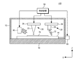
- FIG. 1 shows an example of the configuration of the solder ball supply device 100.
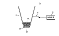
- FIG. 2 shows an example of the configuration of the solder transfer unit 20 constituting the solder ball supply device 100.
- the horizontal direction of the paper surface is the X direction
- the vertical direction of the paper surface is the Z direction
- the X direction and the direction orthogonal to the Z direction are the Y direction.
- the solder ball supply device 100 includes a control device 50 that controls the operation of the entire device, a base 10, and a case 12 that covers the substrate mounting surface side of the base 10.
- the control device 50 has a CPU (Central Processing Unit) and a ROM (Read Only Memory) (not shown), and activates a program stored in the ROM to control each unit to control solder ball supply processes and solder described later. Each step of bump formation is executed.
- CPU Central Processing Unit
- ROM Read Only Memory
- a stage 14 a solder transfer part 20, a solder filling part 30, and an ionizer 40 are provided.
- the stage 14 places a substrate 70 on which a resist 74 is placed.
- a vibration device 60 is attached to the stage 14.
- the vibration device 60 is driven based on the control of the control device 50 when the solder ball SBL is shaken off by the hopper 22 or when the solder ball SBL is filled by the squeegee 32 to vibrate the stage 14.
- the vibration direction may be, for example, oscillated in the XY plane.
- the solder balls SBL in the openings 76 can be densely filled, and as a result, the filling rate of the solder balls SBL can be increased.
- the solder transfer part 20 has a hopper 22, a net 24, an ultrasonic transmitter 26, and a moving mechanism 28 (see FIG. 1).
- the hopper 22 is a truncated cone-shaped cylinder provided above the substrate 70, and is attached to the moving mechanism 28 so that the surface side with a smaller area faces downward.
- the moving mechanism 28 is composed of, for example, an XYZ stage, and enables the hopper 22 to move in the XYZ directions by driving a motor (not shown) under the control of the control device 50.
- a plurality of solder balls SBL are accommodated in the hopper 22.
- a predetermined amount of the solder ball SBL may be automatically supplied using a supply device (not shown), or the user manually supplies the solder ball SBL. You may do it.
- solder ball SBL used in this example, a lead-free solder having a particle diameter of, for example, 1 to 10 ⁇ m and a metal composition of Sn—Ag—Cu can be used. Specifically, a lead-free solder of 3.0Ag-0.5Cu-residual Sn can be suitably used.
- the solder balls SBL may be made of lead-free solder such as Sn—Zn—Bi, Sn—Cu, Sn—Ag—In—Bi, or Sn—Zn—Al. Sn-Pb-based and Sn-Pb-Ag-based lead-containing solders may be used.
- the solder composition used in the present invention is not limited to the solder composition.
- the net 24 is attached to the lower end of the hopper 22 and has a fine lattice-shaped opening.
- the diameter of the opening is selected to be equal to or slightly larger than the particle diameter of the solder ball SBL to be used.
- the net 24 can be configured to be detachable from the hopper 22. Thereby, the net
- the shape of the swinging portion 23 at the tip of the hopper 22 is circular in this example.
- the ultrasonic transmitter 26 is attached to, for example, a side surface of the hopper 22 and vibrates the hopper 22 at a frequency of, for example, 20 to 40 kHz based on the control of the control device 50. Thereby, the plurality of solder balls SBL accommodated in the hopper 22 can be shaken off onto the resist 74 uniformly and uniformly. Further, since the diameter of the opening of the aperture 24 is equal to or slightly larger than the spherical shape of the solder ball SBL to be used, it can be made to function as a shutter by turning on / off the ultrasonic transmitter 26.
- the solder filling portion 30 includes a squeegee 32, a fixing portion 34, and a moving mechanism 36.
- the squeegee 32 is made of urethane, for example, and is attached to the moving mechanism 36 via a fixed portion 34.
- the moving mechanism 36 is, for example, an XYZ stage, and the squeegee 32 can be moved in the XYZ directions by driving a motor (not shown) under the control of the control device 50.
- the ionizer 40 is installed on one end side of the substrate 70 placed on the stage 14 so that the air outlet faces the solder balls SBL and the substrate 70 shaken down on the upper surface of the resist 74 and the opening 76.
- the ionizer 40 operates under the control of the control device 50 to spray positive ions and negative ions onto the solder balls SBL and the substrate 70.
- the positive ions or the like may be sprayed before the solder ball SBL is shaken off on the resist 74.
- the static electricity of the solder balls SBL and the substrate 70 is neutralized by neutralizing the bias of the charges of the solder balls SBL and the substrate 70, and the solder balls SBL are aggregated during filling of the openings 76 of the solder balls SBL.
- the ionizer 40 can also be configured to swing.
- solder bump formation method (example of solder ball supply method)
- solder ball supply method an example of a method for forming the solder bump SBP according to the present invention
- FIGS. 1 to 3H show an example of a process for forming the solder bump SBP.
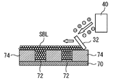
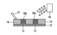
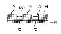
- 3A to 3E show an example of a process for supplying the solder ball SBL to the opening 76 of the resist 74.
- a plurality of electrodes 72 having a diameter of 10 to 30 ⁇ m are formed on the substrate 70, and the pitch between the electrodes 72 and 72 is selected to be 20 to 60 ⁇ m.
- a substrate 70 is prepared in which a resist 74 having an opening 76 is disposed at a position corresponding to the electrode 72 of the substrate 70.
- a known photolithography technique can be used for patterning the resist 74. Specifically, a resist 74 is applied on the substrate 70, and the pattern of the opening 76 is transferred by irradiating the applied resist 74 with light through a photomask. Subsequently, an opening 76 is formed on the electrode 72 of the resist 74 by removing the resist 74 in the exposed portion.
- the resist 74 has been described as an example using a positive type, a negative type may be used.
- the thickness of the resist 74 is preferably about twice the thickness of the target solder bump SBP, as will be described later. This is because when the plurality of solder balls SBL filled in the openings 76 of the resist 74 are melted, the height becomes about 1 ⁇ 2 of the height of the plurality of solder balls SBL at the time of filling.
- the resist 74 is generally made of a material that can withstand a temperature in a reflow apparatus 200 described later and can be peeled off from the substrate 70 by a specific solvent.
- a plurality of solder balls SBL are shaken down from the hopper 22 into the openings 76 of the resist 74 and filled.
- the control device 50 drives the ultrasonic transmitter 26 to vibrate the hopper 22 at a frequency of 20 to 40 kHz, for example, and shakes the plurality of solder balls SBL from the aperture 24 to the opening 76. Further, the control device 50 drives the moving mechanism 28 to move the hopper 22 in the substrate plane direction (XY direction), and uniformly shakes the solder balls SBL over the entire surface of the resist 74.
- control device 50 performs static elimination by driving the ionizer 40 and spraying plus / minus ions onto the falling solder ball SBL and the solder ball SBL shaken onto the resist 74.
- control device 50 may drive the vibration device 60 to vibrate the stage 14.
- the filling step is performed under atmospheric pressure, but may be performed under vacuum or the like.
- the solder balls SBL can be uniformly and densely filled into all the openings 76 while preventing aggregation of the plurality of solder balls SBL.
- the plurality of solder balls SBL are also shaken off and deposited on the upper surface of the resist 74 other than the opening 76.
- the filling of the solder ball SBL into the opening 76 can be controlled with high accuracy by appropriately adjusting the frequency of the ultrasonic transmitter 26, the moving speed of the hopper 22, and the amount of ions blown from the ionizer 40. .
- the squeegee 32 is slid in the XY direction on the upper surface of the resist 74 while the ionizer 40 is driven, and the solder balls SBL shaken off other than the openings 76 are removed from the resist. 74 is removed by scraping from the upper surface. Further, by passing the squeegee 32 over the opening 76, the solder balls SBL inside and around the opening 76 are pushed into the opening 76 by the squeegee 32. Thereby, the density of the solder balls SBL in the opening 76 can be increased.
- the squeegee 32 has a function of increasing the filling rate of the solder ball SBL with respect to the opening 76 in addition to the function of removing the excess solder ball SBL. Further, the spraying of positive ions or the like by the ionizer 40 prevents the solder balls SBL from agglomerating, and the filling of the openings 76 and the removal of the excess solder balls SBL can be performed smoothly.
- the substrate 70 is taken out from the solder ball supply device 100, and the taken-out substrate 70 is conveyed to the reflow device 200 as shown in FIG. 3F.
- the reflow apparatus 200 heats and melts the plurality of solder balls SBL in a mixed gas atmosphere of an organic acid gas and an inert gas.
- the solder ball SBL and the oxide of the electrode 72 are removed by the reducing power of the organic acid in the reflow apparatus 200. Therefore, the conventionally required flux is not required.
- solder bumps SBP are formed on the respective electrodes 72 as shown in FIG. 3G.
- organic acid gas examples include, for example, formic acid, acetic acid, propionic acid, butyric acid, haleric acid, caproic acid, enanthic acid, caprylic acid, pelargonic acid, succinic acid, malonic acid, succinic acid, acrylic acid, salicylic acid, lactic acid, Any one gas or two or more mixed gases obtained by heating and vaporizing diacetyl, acetylacetone, and acetonylacetone can be used.
- the inert gas examples include nitrogen, carbon dioxide, helium, and argon.
- the substrate 70 is taken out from the reflow apparatus 200, and as shown in FIG. 3H, the resist 74 is peeled off from the substrate 70 and cleaned using a solvent. In this way, the solder bump SBP can be formed on each electrode 72 of the substrate 70.
- FIG. 4A is a view showing a state when a solder ball SBL having a particle size S1 of 2 ⁇ m is filled in the opening 76
- FIG. 4B shows a state of a solder bump SBP obtained after reflow.
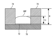
- the diameter R of the electrode 72 is 10 ⁇ m
- the pitch between the electrodes 72 and 72 is 20 ⁇ m
- the thickness of the target solder bump SBP is 5.3 ⁇ m.
- the solder ball SBL having a particle size S1 of 1/5 or less of the diameter R of the electrode 72 was used. Specifically, solder balls SBL having a particle size of 2 ⁇ m were used. Further, the height 74 of the resist 74 was formed to 10 ⁇ m, which is about twice the thickness (5.3 ⁇ m) of the solder bump SBP. Under such conditions, when the solder balls SBL were filled into the openings 76, the filling rate of the plurality of solder balls SBL into the openings 76 was 43.2%, as shown in FIG. 4A.
- the target thickness T1 of the solder bump SBP became 5.3 ⁇ m as shown in FIG. 4B.
- the filling rate of the solder ball SBL into the opening 76 can be increased, and the target thickness of the solder bump SBP can be realized.
- FIG. 5A is a view when the opening 76 is filled with solder balls SBL having a particle size S2 of 3 ⁇ m
- FIG. 5B is a view showing solder bumps SBP obtained after reflow.
- the diameter R of the other electrodes, the height H of the resist 74, and the target thickness of the solder bump SBP were set to the same conditions as in the case of using the solder ball SBL having a particle size S1 of 2 ⁇ m.
- the filling rate of the openings 76 of the plurality of solder balls SBL is 36.0%. It became.
- the thickness T2 of the solder bump SBP was 4.58 ⁇ m as shown in FIG. 5B.
- the solder ball SBL is shaken off from the hopper 22 provided above the substrate 70 to the opening 76, and then the squeegee 32 is shaken off by movement in the XY direction. Since the solder balls SBL are filled into the openings 76, the solder balls SBL can be filled into the openings 76 efficiently and smoothly even if the pitch of the electrodes 72 is fine. At this time, since the solder balls SBL are shaken down evenly over the entire surface of the resist 74 while moving the hopper 22 in the XY directions, the solder balls SBL can be uniformly filled in all the openings 76. it can.
- the height and width of the solder bump SBP can be easily controlled by changing the height and width of the opening 76 of the resist 74.
- solder bump SBP when the solder bump SBP is formed, reflow is performed using an organic acid, so that fluxless reflow can be realized. In addition, since no flux is used, the generation of voids during reflow that generally occurs in solder paste can be suppressed.
- the resist 74 is provided between the electrodes 72 when the solder bump SBP is formed, the occurrence of a bridge can be suppressed.
- the technical scope of the present invention is not limited to the above-described embodiment, and includes those in which various modifications are made to the above-described embodiment without departing from the spirit of the present invention.
- the resist 74 is used as the mask member, but the present invention is not limited to this.
- a metal mask or the like can be used as the mask member.
- the frequency of the ultrasonic transmitter 26 is not limited to 20 to 40 kHz, and can be appropriately selected in other frequency bands.
- the shape of the hopper 22 is not limited to a truncated cone shape, and any shape that can accommodate a plurality of solder balls SBL can be adopted as appropriate.
- the solder ball SBL is shaken off from the hopper 22 to the opening 76, and then the solder ball SBL shaken off by the squeegee 32 is filled into the opening 76. Therefore, even when the diameter of the electrode 72 is reduced, The solder ball SBL can be supplied to the opening 76 smoothly and smoothly. Further, according to the present invention, even when the electrodes 72 having a plurality of types of shapes (circular, rectangular, elliptical, etc.) and areas exist on the same substrate 70, the plurality of solder balls SBL are used, so that it is efficient and smooth. In addition, the solder ball SBL can be supplied to the opening 76. Thereby, a plurality of types of solder bumps SBP can be formed on the same substrate 70.
Landscapes
- Engineering & Computer Science (AREA)
- Mechanical Engineering (AREA)
- Electric Connection Of Electric Components To Printed Circuits (AREA)
Abstract
Description
本発明において、電極の一辺または直径は10~30μmであることが好ましい。また、はんだボールの粒径は1~10μmの粒径であることが好ましい。
本発明において、電極の一辺または直径は10~30μmであることが好ましい。また、はんだボールの粒径は1~10μmの粒径であることが好ましい。
本発明において、電極の一辺または直径は10~30μmであることが好ましい。また、はんだボールの粒径は1~10μmの粒径であることが好ましい。
まず、本発明に係るはんだボール供給装置100の構成例について説明する。図1は、はんだボール供給装置100の構成の一例を示している。図2は、はんだボール供給装置100を構成するはんだ振込部20の構成の一例を示している。なお、図1において、紙面の水平方向をX方向とし、紙面の垂直方向をZ方向とし、X方向およびZ方向に直交する方向をY方向としている。
次に、本発明に係るはんだバンプSBPの形成方法の一例について図1~図3Hを参照して説明する。図3A~図3Hは、はんだバンプSBPを形成する工程の一例を示している。このうち、図3A~図3Eは、はんだボールSBLをレジスト74の開口部76に供給する工程の一例を示している。なお、本例では、基板70上には10~30μmの直径からなる複数の電極72が形成され、電極72,72間のピッチは20~60μmに選定されているものとする。
次に、はんだボールSBLの粒径S1と電極72の直径Rとの関係等の一例について説明する。図4Aは粒径S1が2μmのはんだボールSBLを開口部76に充填したときの状態を示す図であり、図4Bはリフロー後に得られるはんだバンプSBPの状態を示している。
また本発明によれば、同一の基板70上に複数種類の形状(円形、矩形、楕円等)および面積を有する電極72が存在した場合でも、複数のはんだボールSBLを用いるので、効率的かつ円滑にはんだボールSBLを開口部76に供給することができる。これにより、同一の基板70上に複数種類の形状のはんだバンプSBPを形成することができる。
32 スキージ
40 イオナイザー
70 基板
74 レジスト
76 開口部
SBL はんだボール
SBP はんだバンプ
Claims (14)
- 電極を有する基板上に配置されたマスク部材の開口部にはんだボールを供給するはんだボール供給方法であって、
前記基板の上方に設けられたホッパーから前記電極上に形成される前記開口部に対して複数のはんだボールを振り落す第1の工程と、
前記マスク部材の平面方向にスキージを移動させることで前記開口部に振り落された複数の前記はんだボールを前記開口部に充填する第2の工程と
を有するはんだボール供給方法。 - 前記電極の一辺または直径が10~30μmからなる
請求項1に記載のはんだボール供給方法。 - 前記はんだボールの粒径が1~10μmの粒径からなる
請求項1または2に記載のはんだボール供給方法。 - 前記第1および第2の工程において、少なくとも前記マスク部材に振り落とされる複数の前記はんだボールの静電気を除去する
請求項1に記載のはんだボール供給方法。 - 前記第2の工程において、前記マスク部材に振り落とされた複数の前記はんだボールを前記スキージを用いて前記マスク部材上から除去する
請求項1または2に記載のはんだボール供給方法。 - 電極を有する基板上に配置されたマスク部材の開口部にはんだボールを供給するはんだボール供給装置であって、
前記基板の上方に設けられ、前記電極上に形成される前記開口部にはんだボールを振り落すホッパーと、
前記マスク部材の平面方向に移動することで前記開口部に振り落された複数の前記はんだボールを前記開口部に充填するスキージと
を備えるはんだボール供給装置。 - 前記電極の一辺または直径が10~30μmからなる
請求項6に記載のはんだボール供給装置。 - 前記はんだボールの粒径が1~10μmの粒径からなる
請求項6または7に記載のはんだボール供給装置。 - 少なくとも複数の前記はんだボールの静電気を除去するイオナイザーを備える
請求項6に記載のはんだボール供給装置。 - 電極を有する基板上に配置されたマスク部材の前記電極上に形成される開口部に前記基板の上方に設けられたホッパーから複数のはんだボールを振り落す第1の工程と、
前記マスク部材の平面方向にスキージを移動させることで前記開口部に振り落された複数の前記はんだボールを前記開口部に充填する第2の工程と、
有機酸ガスを用いて前記開口部に充填された複数の前記はんだボールを溶融することにより前記電極上にはんだバンプを形成する第3の工程と
を有するはんだバンプ形成方法。 - 前記電極の一辺または直径が10~30μmからなる
請求項10に記載のはんだバンプ形成方法。 - 前記はんだボールの粒径が1~10μmの粒径からなる
請求項10または11に記載のはんだバンプ形成方法。 - 少なくとも複数の前記はんだボールの静電気を除去する工程を有する
請求項10に記載のはんだバンプ形成方法。 - 前記第3の工程が終了した後に、前記基板上に配置された前記マスク部材を除去する第4の工程を有する
請求項10に記載のはんだバンプ形成方法。
Priority Applications (4)
| Application Number | Priority Date | Filing Date | Title |
|---|---|---|---|
| US14/392,168 US10722965B2 (en) | 2013-06-26 | 2013-06-26 | Solder ball supplying method, solder ball supplying device, and solder bump forming method |
| PCT/JP2013/067504 WO2014207835A1 (ja) | 2013-06-26 | 2013-06-26 | はんだボール供給方法、はんだボール供給装置およびはんだバンプ形成方法 |
| JP2015523710A JP5880785B2 (ja) | 2013-06-26 | 2013-06-26 | はんだボール供給方法、はんだボール供給装置およびはんだバンプ形成方法 |
| TW103121145A TWI604910B (zh) | 2013-06-26 | 2014-06-19 | A solder ball supplying method, a solder ball supplying device, and a solder bump forming method |
Applications Claiming Priority (1)
| Application Number | Priority Date | Filing Date | Title |
|---|---|---|---|
| PCT/JP2013/067504 WO2014207835A1 (ja) | 2013-06-26 | 2013-06-26 | はんだボール供給方法、はんだボール供給装置およびはんだバンプ形成方法 |
Publications (1)
| Publication Number | Publication Date |
|---|---|
| WO2014207835A1 true WO2014207835A1 (ja) | 2014-12-31 |
Family
ID=52141241
Family Applications (1)
| Application Number | Title | Priority Date | Filing Date |
|---|---|---|---|
| PCT/JP2013/067504 Ceased WO2014207835A1 (ja) | 2013-06-26 | 2013-06-26 | はんだボール供給方法、はんだボール供給装置およびはんだバンプ形成方法 |
Country Status (4)
| Country | Link |
|---|---|
| US (1) | US10722965B2 (ja) |
| JP (1) | JP5880785B2 (ja) |
| TW (1) | TWI604910B (ja) |
| WO (1) | WO2014207835A1 (ja) |
Families Citing this family (4)
| Publication number | Priority date | Publication date | Assignee | Title |
|---|---|---|---|---|
| JP7041953B2 (ja) * | 2017-07-28 | 2022-03-25 | アスリートFa株式会社 | 柱状部材搭載装置及び柱状部材搭載方法 |
| JP7513873B2 (ja) * | 2019-04-30 | 2024-07-10 | デクセリアルズ株式会社 | 摺動装置 |
| KR102696530B1 (ko) * | 2019-04-30 | 2024-08-19 | 데쿠세리아루즈 가부시키가이샤 | 슬라이딩 대상물의 표면에 대한 슬라이딩 처리물의 공급 또는 배제 방법 |
| CN112091346B (zh) * | 2020-09-07 | 2022-08-19 | 昆山联滔电子有限公司 | 一种激光喷射焊球的焊接方法 |
Citations (5)
| Publication number | Priority date | Publication date | Assignee | Title |
|---|---|---|---|---|
| JPH08153960A (ja) * | 1994-11-28 | 1996-06-11 | Matsushita Electric Ind Co Ltd | 半田ボールの搭載装置および搭載方法 |
| WO2006004000A1 (ja) * | 2004-06-30 | 2006-01-12 | Athlete Fa Corporation | 導電性ボールの搭載方法および装置 |
| JP2007125578A (ja) * | 2005-11-02 | 2007-05-24 | Fujitsu Ltd | リフロー装置、リフロー方法、および半導体装置の製造方法 |
| JP2009081398A (ja) * | 2007-09-27 | 2009-04-16 | Fujitsu Microelectronics Ltd | 電極の形成方法及び半導体装置の製造方法 |
| JP2010004060A (ja) * | 2009-08-12 | 2010-01-07 | Athlete Fa Kk | ボール振込装置 |
Family Cites Families (15)
| Publication number | Priority date | Publication date | Assignee | Title |
|---|---|---|---|---|
| US6293456B1 (en) * | 1997-05-27 | 2001-09-25 | Spheretek, Llc | Methods for forming solder balls on substrates |
| JP4253748B2 (ja) * | 1998-12-25 | 2009-04-15 | 澁谷工業株式会社 | 半田ボール等の供給装置 |
| TW522540B (en) * | 2002-02-27 | 2003-03-01 | Advanced Semiconductor Eng | Solder ball manufacturing process |
| TW521361B (en) * | 2002-02-27 | 2003-02-21 | Advanced Semiconductor Eng | Bump process |
| CN1477703A (zh) * | 2002-08-02 | 2004-02-25 | ǧס������ҵ��ʽ���� | 焊球组件及其生产方法,形成焊块的方法 |
| JP3959336B2 (ja) * | 2002-11-08 | 2007-08-15 | ユー・エム・シー・ジャパン株式会社 | バンプボール圧着装置 |
| US6871776B2 (en) * | 2003-03-10 | 2005-03-29 | Trucco Horacio Andres | Manufacture of solid-solder-deposit PCB utilizing electrically heated wire mesh |
| JP4458835B2 (ja) | 2003-12-15 | 2010-04-28 | 東レエンジニアリング株式会社 | 半田バンプの形成方法及びその装置 |
| KR100958554B1 (ko) * | 2004-12-20 | 2010-05-17 | 센주긴조쿠고교 가부시키가이샤 | 땜납 프리코트 방법 및 전자기기용 워크 |
| US7476976B2 (en) | 2005-02-23 | 2009-01-13 | Texas Instruments Incorporated | Flip chip package with advanced electrical and thermal properties for high current designs |
| JP4320350B2 (ja) * | 2006-08-23 | 2009-08-26 | Tdk株式会社 | 導電性部材供給装置及び導電性部材供給方法 |
| US20080296355A1 (en) * | 2007-05-31 | 2008-12-04 | Texas Instruments Incorporated | Direct ball dispenser |
| TWI462676B (zh) * | 2009-02-13 | 2014-11-21 | 千住金屬工業股份有限公司 | The solder bumps for the circuit substrate are formed using the transfer sheet |
| JP5462712B2 (ja) | 2010-05-24 | 2014-04-02 | 株式会社日立製作所 | マイクロバンプ形成装置 |
| WO2012063386A1 (ja) * | 2010-11-08 | 2012-05-18 | パナソニック株式会社 | はんだ転写基材の製造方法、はんだプリコート方法、及びはんだ転写基材 |
-
2013
- 2013-06-26 JP JP2015523710A patent/JP5880785B2/ja active Active
- 2013-06-26 WO PCT/JP2013/067504 patent/WO2014207835A1/ja not_active Ceased
- 2013-06-26 US US14/392,168 patent/US10722965B2/en active Active
-
2014
- 2014-06-19 TW TW103121145A patent/TWI604910B/zh active
Patent Citations (5)
| Publication number | Priority date | Publication date | Assignee | Title |
|---|---|---|---|---|
| JPH08153960A (ja) * | 1994-11-28 | 1996-06-11 | Matsushita Electric Ind Co Ltd | 半田ボールの搭載装置および搭載方法 |
| WO2006004000A1 (ja) * | 2004-06-30 | 2006-01-12 | Athlete Fa Corporation | 導電性ボールの搭載方法および装置 |
| JP2007125578A (ja) * | 2005-11-02 | 2007-05-24 | Fujitsu Ltd | リフロー装置、リフロー方法、および半導体装置の製造方法 |
| JP2009081398A (ja) * | 2007-09-27 | 2009-04-16 | Fujitsu Microelectronics Ltd | 電極の形成方法及び半導体装置の製造方法 |
| JP2010004060A (ja) * | 2009-08-12 | 2010-01-07 | Athlete Fa Kk | ボール振込装置 |
Also Published As
| Publication number | Publication date |
|---|---|
| TWI604910B (zh) | 2017-11-11 |
| TW201524653A (zh) | 2015-07-01 |
| JP5880785B2 (ja) | 2016-03-09 |
| JPWO2014207835A1 (ja) | 2017-02-23 |
| US10722965B2 (en) | 2020-07-28 |
| US20160271715A1 (en) | 2016-09-22 |
Similar Documents
| Publication | Publication Date | Title |
|---|---|---|
| US5159171A (en) | Method and apparatus for solder laser printing | |
| TWI480965B (zh) | Solder ball inspection repair device and solder ball detection repair method | |
| TWI418436B (zh) | A solder ball printing apparatus and a solder ball printing method | |
| JP5880785B2 (ja) | はんだボール供給方法、はんだボール供給装置およびはんだバンプ形成方法 | |
| CN105914165B (zh) | 基板处理装置、基板处理系统以及基板处理方法 | |
| TW200900246A (en) | Screen printing device and bump forming method | |
| JP4720608B2 (ja) | 部品実装装置および部品実装方法 | |
| JPH11297886A (ja) | はんだバンプ形成方法 | |
| JP2010182983A (ja) | 部品実装装置および部品実装方法 | |
| JP3860355B2 (ja) | 半田バンプの形成方法 | |
| JP3829612B2 (ja) | 半田バンプ形成装置および半田バンプ形成方法ならびに半田ペースト印刷装置および半田ペースト印刷方法 | |
| JP2008060438A (ja) | 電子部品実装装置および電子部品実装方法 | |
| JPWO2017104746A1 (ja) | はんだバンプの修正方法 | |
| JP5535122B2 (ja) | フラックス塗布方法、実装基板の製造方法およびフラックス塗布装置 | |
| CN100531522C (zh) | 丝网印刷装置及丝网印刷方法 | |
| EP4066976A1 (en) | Component mounting method, and component mounting system | |
| JPH09246706A (ja) | ハンダ供給方法及び部品実装基板の製造方法 | |
| JP7022888B2 (ja) | 部品実装方法および部品実装基板の製造方法 | |
| JP4053907B2 (ja) | フラックス供給方法及び装置、バンプ形成方法、コンピュータプログラム、並びにコンピュータ読み取り可能な記憶媒体 | |
| JP2013098467A (ja) | 二次ノズル体と噴流式ハンダ付け方法と噴流式ハンダ付け装置 | |
| JP2004096042A (ja) | 回路基板上への接続材料の供給方法及び供給装置 | |
| CN114245606B (zh) | 一种新型的封装外壳焊料预置方法 | |
| JP7199507B2 (ja) | 成膜装置及び実装機 | |
| JP2004186425A (ja) | 半田付け装置および半田付け方法 | |
| JP4457354B2 (ja) | 導電性ボールの搭載装置及び導電性ボールの搭載装置に組み込まれる整列部材 |
Legal Events
| Date | Code | Title | Description |
|---|---|---|---|
| 121 | Ep: the epo has been informed by wipo that ep was designated in this application |
Ref document number: 13887602 Country of ref document: EP Kind code of ref document: A1 |
|
| ENP | Entry into the national phase |
Ref document number: 2015523710 Country of ref document: JP Kind code of ref document: A |
|
| NENP | Non-entry into the national phase |
Ref country code: DE |
|
| WWE | Wipo information: entry into national phase |
Ref document number: 14392168 Country of ref document: US |
|
| 122 | Ep: pct application non-entry in european phase |
Ref document number: 13887602 Country of ref document: EP Kind code of ref document: A1 |