WO2014196165A1 - 半導体装置の保護回路 - Google Patents
半導体装置の保護回路 Download PDFInfo
- Publication number
- WO2014196165A1 WO2014196165A1 PCT/JP2014/002813 JP2014002813W WO2014196165A1 WO 2014196165 A1 WO2014196165 A1 WO 2014196165A1 JP 2014002813 W JP2014002813 W JP 2014002813W WO 2014196165 A1 WO2014196165 A1 WO 2014196165A1
- Authority
- WO
- WIPO (PCT)
- Prior art keywords
- thyristor
- resistor
- voltage
- gate
- protection circuit
- Prior art date
- Legal status (The legal status is an assumption and is not a legal conclusion. Google has not performed a legal analysis and makes no representation as to the accuracy of the status listed.)
- Ceased
Links
Images




Classifications
-
- H—ELECTRICITY
- H03—ELECTRONIC CIRCUITRY
- H03K—PULSE TECHNIQUE
- H03K17/00—Electronic switching or gating, i.e. not by contact-making and –breaking
- H03K17/08—Modifications for protecting switching circuit against overcurrent or overvoltage
- H03K17/081—Modifications for protecting switching circuit against overcurrent or overvoltage without feedback from the output circuit to the control circuit
- H03K17/0812—Modifications for protecting switching circuit against overcurrent or overvoltage without feedback from the output circuit to the control circuit by measures taken in the control circuit
- H03K17/08122—Modifications for protecting switching circuit against overcurrent or overvoltage without feedback from the output circuit to the control circuit by measures taken in the control circuit in field-effect transistor switches
-
- H—ELECTRICITY
- H02—GENERATION; CONVERSION OR DISTRIBUTION OF ELECTRIC POWER
- H02H—EMERGENCY PROTECTIVE CIRCUIT ARRANGEMENTS
- H02H7/00—Emergency protective circuit arrangements specially adapted for specific types of electric machines or apparatus or for sectionalised protection of cable or line systems, and effecting automatic switching in the event of an undesired change from normal working conditions
- H02H7/003—Emergency protective circuit arrangements specially adapted for specific types of electric machines or apparatus or for sectionalised protection of cable or line systems, and effecting automatic switching in the event of an undesired change from normal working conditions for electrostatic apparatus
-
- H—ELECTRICITY
- H10—SEMICONDUCTOR DEVICES; ELECTRIC SOLID-STATE DEVICES NOT OTHERWISE PROVIDED FOR
- H10D—INORGANIC ELECTRIC SEMICONDUCTOR DEVICES
- H10D30/00—Field-effect transistors [FET]
- H10D30/40—FETs having zero-dimensional [0D], one-dimensional [1D] or two-dimensional [2D] charge carrier gas channels
- H10D30/47—FETs having zero-dimensional [0D], one-dimensional [1D] or two-dimensional [2D] charge carrier gas channels having two-dimensional [2D] charge carrier gas channels, e.g. nanoribbon FETs or high electron mobility transistors [HEMT]
-
- H—ELECTRICITY
- H10—SEMICONDUCTOR DEVICES; ELECTRIC SOLID-STATE DEVICES NOT OTHERWISE PROVIDED FOR
- H10D—INORGANIC ELECTRIC SEMICONDUCTOR DEVICES
- H10D84/00—Integrated devices formed in or on semiconductor substrates that comprise only semiconducting layers, e.g. on Si wafers or on GaAs-on-Si wafers
- H10D84/101—Integrated devices comprising main components and built-in components, e.g. IGBT having built-in freewheel diode
- H10D84/131—Thyristors having built-in components
- H10D84/133—Thyristors having built-in components the built-in components being capacitors or resistors
-
- H—ELECTRICITY
- H10—SEMICONDUCTOR DEVICES; ELECTRIC SOLID-STATE DEVICES NOT OTHERWISE PROVIDED FOR
- H10D—INORGANIC ELECTRIC SEMICONDUCTOR DEVICES
- H10D84/00—Integrated devices formed in or on semiconductor substrates that comprise only semiconducting layers, e.g. on Si wafers or on GaAs-on-Si wafers
- H10D84/101—Integrated devices comprising main components and built-in components, e.g. IGBT having built-in freewheel diode
- H10D84/131—Thyristors having built-in components
- H10D84/135—Thyristors having built-in components the built-in components being diodes
-
- H—ELECTRICITY
- H10—SEMICONDUCTOR DEVICES; ELECTRIC SOLID-STATE DEVICES NOT OTHERWISE PROVIDED FOR
- H10D—INORGANIC ELECTRIC SEMICONDUCTOR DEVICES
- H10D89/00—Aspects of integrated devices not covered by groups H10D84/00 - H10D88/00
- H10D89/60—Integrated devices comprising arrangements for electrical or thermal protection, e.g. protection circuits against electrostatic discharge [ESD]
Definitions
- the present disclosure relates to a protection circuit for a semiconductor device having a semiconductor switching element composed of a high electron mobility transistor (hereinafter referred to as HEMT).
- HEMT high electron mobility transistor
- the avalanche energy tolerance is an index of the breakdown tolerance of the device, and is defined as the maximum energy that can be consumed without destroying the device when energy accumulated in the inductive load is consumed by the device.
- GaN-HEMT or GaAs-HEMT made of a compound semiconductor is applied as a semiconductor switching element, normally, energy from an inductive load cannot be consumed inside the element, and the gate-drain tolerance (BVgd) The breakdown voltage exceeds the off-state breakdown voltage (Bvdsoff), leading to element destruction. Therefore, in an inductive load system having a self-inductance L such as an inverter, it is usually used together with a protection element.
- an external diode is connected in reverse parallel as a protective element between the source and drain of the HEMT.
- this method by providing an external diode, a structure similar to that of a silicon MOSFET is realized, and energy from an inductive load is consumed.
- the energy when the HEMT is turned off from the state in which the rated current is flowing to the HEMT is consumed on the diode side, it is required that a current as large as the HEMT flows in the diode. There is a problem that it becomes large in size.
- Patent Document 1 proposes a structure in which Zener diodes are connected in reverse parallel as protective elements between the gate and drain and between the source and gate.
- the zener diode between the source and the gate also breaks down simultaneously with the breakdown of the zener diode between the gate and the drain, and a breakdown current flows.
- a voltage divided according to the number of stages of the Zener diode is applied to the HEMT as a gate voltage.
- charging the gate opens the channel and turns on the HEMT. That is, the energy of the inductive load is consumed by the HEMT by turning on the HEMT.
- the Zener diode should just be the structure through which a small electric current which drives a HEMT flows, the size of a diode can be made small.
- Patent Document 1 requires a current sufficient to supply enough power to drive the gate.
- a very large number of diodes are required. For example, if an attempt is made to obtain a blocking voltage of several hundred volts [V], the number of diode stages becomes several tens to several hundreds, which is very large.
- V volts
- the protection state a breakdown current flows, but even with the breakdown current, the current flows in the reverse direction to the diode having a large number of stages, and thus the resistance becomes very large. Therefore, the current value does not increase as expected, and the diode must be enlarged in order to pass a current sufficient to drive the semiconductor switching element.
- a diode is connected in parallel in the forward direction as a protection element between the gate and drain and between the source and gate.
- a relatively large current can flow. become.
- the number of diodes must be further increased, and the diode becomes large.
- the number of diode stages can be reduced by connecting MIS transistors in parallel between the gate and the drain and between the source and the gate instead of the diode.
- the current that can be flown when the MIS transistor breaks down during surge protection is not large, and a large MIS transistor is required to flow a sufficient current to drive the gate of the semiconductor switching element. That is, such a structure assumes a low breakdown voltage and is not a structure suitable for a high breakdown voltage.
- This indication aims at providing the protection circuit of the semiconductor device which can obtain avalanche energy tolerance, suppressing the increase in the size of a protection element in view of the said point.
- a protection circuit for a semiconductor device includes a high electron mobility transistor and a protection element.
- the high electron mobility transistor is connected to a load and serves as a semiconductor switching element that controls on / off of power supply to the load.
- the protection element includes a thyristor connected in a forward direction between a drain and a gate of the high electron mobility transistor, and a first resistor connected in series to the thyristor.
- the protection element includes a second resistor and a blocking unit connected in series to the second resistor between a source and a gate of the high electron mobility transistor. The blocking unit cuts off a current flow between the drain and the gate when the thyristor is turned off and allows a current flow between the drain and the gate when the thyristor is turned on.
- the protection circuit of the semiconductor device can obtain an avalanche energy resistance while suppressing an increase in the size of the protection element.
- FIG. 1 is a circuit diagram of a protection circuit of the semiconductor device according to the first embodiment of the present disclosure.
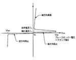
- FIG. 2 is a diagram showing a characteristic line showing the relationship between the voltage V AK and the current I between the anode and the cathode of the thyristor.
- FIG. 3 is a diagram showing the relationship between the characteristic line and the load line shown in FIG.
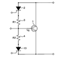
- FIG. 4 is a circuit diagram of a protection circuit of a semiconductor device according to another embodiment.
- FIG. 5 is a circuit diagram of a protection circuit of a semiconductor device according to another embodiment.
- FIG. 6 is a circuit diagram of a protection circuit of a semiconductor device according to another embodiment.
- the protection circuit includes a HEMT 1 as a semiconductor switching element to be protected, and includes a protection element between the drain and gate and between the source and gate of the HEMT 1.
- the HEMT 1 is driven on / off based on an external gate drive signal, and controls on / off of power supply to an inductive load (not shown) connected between a drain and a source, for example.
- the HEMT 1 is formed using, for example, a compound semiconductor substrate in which a GaN layer serving as an electron transit layer and an n-type AlGaN layer serving as an electron supply layer are stacked on the surface of a substrate such as Si (111) or GaAs. Yes.
- a recess shape portion is formed on the surface of the AlGaN layer, a gate electrode is disposed in the recess shape portion, and a source electrode and a drain electrode are formed on both sides of the gate electrode.
- the HEMT 1 may be made of any material such as GaN-HEMT or GaAs-HEMT.
- a thyristor 2 and a first resistor 3 connected in series are provided as protective elements.
- the thyristor 2 is disposed on the high side of the first resistor 3 and is forward-connected between the drain and gate of the HEMT 1.
- the thyristor 2 has a pnpn structure and is turned on when a voltage equal to or higher than the breakover voltage V BF (forward withstand voltage) is applied between the anode and the cathode. After turning on, the thyristor 2 maintains the on state even without the base current. The operation is performed.
- the anode of the thyristor 2 - cathode voltage when thyristor 2 is ON, and drops to the voltage Vh negligible compared to the breakover voltage V BF, anode - slightly larger when the current I AC flowing between the cathode increases However, the size is almost negligible.
- the thyristor 2 is turned off when the current I AC flowing between the anode and the cathode falls below the holding current Ih.
- the drain voltage is clamped by turning on the thyristor 2 when the drain voltage of the HEMT 1 becomes a predetermined voltage at the time of turn-off. This prevents a voltage exceeding the clamp voltage from being applied to the HEMT 1.
- the base of the thyristor 2 can be selected to be opened or shorted to the cathode of the thyristor 2 according to the leakage current Is (see FIG. 2) and the withstand voltage. That is, when the base of the thyristor 2 is opened, the leakage current Is is increased, and when the thyristor 2 has a high breakdown voltage, the amount of heat generation increases. On the other hand, when the base of the thyristor 2 is short-circuited to the cathode, the leakage current Is can be reduced as compared with the case where the thyristor 2 is opened. For this reason, in consideration of the heat resistance of the thyristor 2, it is only necessary to select whether the base of the thyristor 2 is opened or shorted to the cathode.
- the first resistor 3 is connected in series with the thyristor 2 and is used together with a second resistor 4 to be described later to determine a current flowing through the thyristor 2 during clamping.
- the first resistor 3 serves as a voltage dividing resistor that divides the drain-source voltage of the HEMT 1 together with the second resistor 4, and thus plays a role of determining the gate voltage Vg of the HEMT 1 at the turn-off time.
- a second resistor 4 and a Zener diode 5 connected in series are provided as protective elements.
- the second resistor 4 is used to determine the current flowing through the thyristor 2 during clamping together with the first resistor 3 as described above. Further, the second resistor 4 serves as a voltage dividing resistor that divides the drain-source voltage of the HEMT 1 together with the first resistor 3, thereby playing a role of determining the gate voltage of the HEMT 1 at the time of turn-off.
- the zener diode 5 corresponds to a cutoff unit, and when the HEMT 1 is turned on to supply power to the load, the gate voltage Vg is applied to the HEMT 1 by being turned off. In addition, the Zener diode 5 is turned on when the HEMT 1 is turned off and is turned on when the thyristor 2 is turned on, thereby allowing the current to flow to the protection element side. In the present embodiment, the Zener diode 5 is set to have a breakdown voltage equal to or higher than the gate voltage when the HEMT 1 is turned on.
- the Zener diode 5 is a back-to-back connection in which the cathodes are connected to each other, so that it is possible to cope with a case where a negative voltage is applied when the HEMT 1 is turned off. Yes.
- the HEMT 1 when the HEMT 1 is turned on based on an external gate drive signal (gate voltage Vg), the inductive load is driven based on power supply from a power source (not shown), and energy is stored in the inductive load. It is in the state that was done. Then, the HEMT 1 is turned off by a change in the gate drive signal, for example, when the gate voltage Vg is switched from the high level to the low level. At this time, the energy stored in the inductive addition needs to be consumed in the circuit.
- gate voltage Vg an external gate drive signal
- the protection circuit since the protection circuit has the above-described configuration, when a voltage higher than the breakover voltage V BF is applied between the anode and the cathode of the thyristor 2 when the HEMT 1 is turned off, the thyristor. 2 is turned on.
- the voltage divided by the first resistor 3 and the second resistor 4 is applied as the gate voltage Vg of the HEMT 1, and the HEMT 1 is turned on.
- the drain voltage of the HEMT 1 can be clamped by the forward breakdown voltage of the thyristor 2, and a voltage exceeding the clamp voltage can be prevented from being applied to the HEMT 1.
- the thyristor 2 performs an operation of maintaining the on state even when there is no base current after the voltage higher than the breakover voltage V BF is applied between the anode and the cathode and the thyristor 2 is turned on. . Then, once the thyristor 2 is the drain voltage is turned on to clamp the voltage drop of the thyristor 2, i.e. the anode - cathode voltage decreases to the voltage Vh negligible compared to the breakover voltage V BF. This voltage increases somewhat as the current I AC flowing between the anode and the cathode increases, but is almost negligible.
- the current flowing through the protection circuit during clamping is determined by the resistance value R1 of the first resistor 3 and the resistance value R2 of the second resistor 4, and by appropriately selecting these resistance values R1 and R2, It is possible to freely design the current flowing through the protection element from a small current to a large current.
- the resistance value when the thyristor 2 is on is small, and in the case of a high withstand voltage element, the withstand voltage of the diode 5 is sufficiently smaller than that of the thyristor 2 and may be ignored. Therefore, as shown in FIG. 3, when the breakover voltage VBF at which the thyristor 2 is turned on is set to the clamp voltage, the load line is a line determined by the resistance values R1 and R2 of the first resistor 3 and the second resistor 4. The slope can be set by these resistance values R1 and R2.
- the resistance values R1 and R2 of the first resistor 3 and the second resistor 4 are reduced, the current flowing through the protection element can be increased, and if the resistance values R1 and R2 are increased, the current flowing through the protection element is reduced to a small current. Can be.
- a load line determined according to the resistance values R1 and R2 of the first resistor 3 and the second resistor 4 is entered in a graph showing the characteristic lines of the thyristor 2, the intersection of these lines is the thyristor. It represents the current I flowing through the protection element when 2 is turned on and the voltage drop across the thyristor 2. That is, the value of the current I at the point where the thyristor 2 and the load line intersect is the current that flows when the thyristor 2 is turned on, and the value of the voltage V AK at that time is the voltage drop across the thyristor 2.
- the same current I as that of the thyristor 2 flows through the first resistor 3 and the second resistor 4, and the voltage obtained by subtracting the voltage drop at the thyristor 2 from the clamp voltage is the first resistor 3 and the second resistor 4.
- And diode 5 small compared to the clamp voltage and almost negligible. Accordingly, if the clamp voltage is set to the breakover voltage V BF at which the thyristor 2 is turned on, the load lines corresponding to the resistance values R1 and R2 of the first resistor 3 and the second resistor 4 are determined, and the thyristor 2
- the current flowing through the protection element when is turned on can be set as appropriate. Thereby, electric power sufficient to drive the HEMT 1 to be protected can also be supplied by adjusting the current flowing through the protection element.
- the thyristor 2 is turned off.
- the HEMT 1 is also turned off by turning off the thyristor 2 and can be automatically returned to the normal off mode.
- the gate voltage Vg during clamping is given by the resistance value R2 / (R1 + R2) ⁇ clamp voltage + diode 5 from the resistance value R1 of the first resistor 3 and the resistance value R2 of the second resistor 4, so that the resistance value R2 It can be set freely by adjusting.
- the protective element includes the thyristor 2 and the first resistor 3 between the drain and the gate of the HEMT 1, and the second resistor 4 and the diode 5 between the source and the gate of the HEMT 1. ing. Therefore, when the HEMT 1 is turned off, the thyristor 2 is turned on so that a current flows to the protection element side. At that time, the HEMT 1 is divided by the gate voltage Vg formed by being divided by the first resistor 3 and the second resistor 4. Can be turned on.
- the energy accumulated in the inductive load is consumed by turning on the HEMT 1 while turning off the HEMT 1 while preventing the voltage exceeding the blocking voltage from being applied to the HEMT 1 using the forward breakdown voltage of the thyristor 2 as a clamp voltage. It becomes possible. Therefore, it is possible to provide a protection circuit for a semiconductor device capable of obtaining an avalanche energy resistance.
- the protection element can be constituted by the thyristor 2, the first resistor 3, the second resistor 4 and the diode 5, and the diode 5 also has a low breakdown voltage enough to drive the gate of the HEMT 1. Since it is sufficient, the number of stages can be reduced. For this reason, it is also possible to suppress an increase in the size of the protective element.
- the thyristor 2 may be arranged on the low side of the first resistor 3 and on the high side of the gate of the HEMT 1.
- a thyristor 10 may be disposed instead of the diode 5 as a blocking portion.
- the thyristor 10 when the HEMT 1 is turned off, the thyristor 10 performs the same operation as the thyristor 2 so that the voltage divided by the first resistor 3 and the second resistor 4 is applied to the gate of the HEMT 1. , HEMT1 can be turned on. Thereby, the effect similar to 1st Embodiment can be acquired. Also in this case, since it is sufficient that the thyristor 2 has a low breakdown voltage enough to drive the gate of the HEMT 1, it is possible to suppress an increase in the size of the protection element.
- the base of the thyristor 10 can also be selected to be opened or shorted to the cathode of the thyristor 10 according to the leakage current Is and the withstand voltage.
- the thyristor 2 may be configured in a plurality of stages.
Landscapes
- Junction Field-Effect Transistors (AREA)
- Electronic Switches (AREA)
- Semiconductor Integrated Circuits (AREA)
- Power Conversion In General (AREA)
- Engineering & Computer Science (AREA)
- Power Engineering (AREA)
Abstract
Description
本開示の第1実施形態にかかる半導体装置の保護回路について説明する。図1に示すように、保護回路は、保護対象となる半導体スイッチング素子としてHEMT1を備えていると共に、HEMT1のドレイン-ゲート間およびソース-ゲート間に保護素子が備えられた構成とされている。
本開示は上記した実施形態に限定されるものではなく、特許請求の範囲に記載した範囲内において適宜変更が可能である。
Claims (10)
- 負荷に対して接続され、該負荷に対する電力供給のオンオフを制御する半導体スイッチング素子となる高電子移動度トランジスタ(1)と、
前記高電子移動度トランジスタのドレイン-ゲート間に、順方向に接続されたサイリスタ(2)および該サイリスタに直列接続された第1抵抗(3)を備えており、前記高電子移動度トランジスタのソース-ゲート間に、第2抵抗(4)および該第2抵抗に対して直列接続された遮断部(5、10)が備えられた保護素子と、を備え、
前記遮断部は、前記サイリスタがオフされているときに前記ドレイン-ゲート間の電流の流れを遮断すると共に前記サイリスタがオンされているときに前記ドレイン-ゲート間の電流の流れを許容する半導体装置の保護回路。 - 前記高電子移動度トランジスタのターンオフ時における該高電子移動度トランジスタのドレイン電圧が前記サイリスタの順方向耐圧をクランプ電圧としてクランプされる請求項1に記載の半導体装置の保護回路。
- 前記クランプが解除される電圧であるクランプ解除電圧が前記第1抵抗の抵抗値R1および前記第2抵抗の抵抗値R2とを合わせた抵抗値(R1+R2)に対して前記サイリスタにおける保持電流Ihを掛けた値((R1+R2)×Ih)に設定されている請求項2に記載の半導体装置の保護回路。
- 前記高電子移動度トランジスタのドレイン電圧が前記クランプ電圧にクランプされているときにおける該高電子移動度トランジスタのゲート電圧(Vg)が前記第1抵抗の抵抗値R1および前記第2抵抗の抵抗値R2より、R2/(R1+R2)×クランプ電圧とされている請求項2または3に記載の半導体装置の保護回路。
- 前記サイリスタが前記第1抵抗のハイサイド側に接続されている請求項1ないし4のいずれか1つに記載の半導体装置の保護回路。
- 前記サイリスタが前記第1抵抗のローサイド側に接続されている請求項1ないし4のいずれか1つに記載の半導体装置の保護回路。
- 前記ソース-ゲート間には前記第2抵抗と共に前記遮断部としてダイオード(5)が接続されている請求項1ないし6のいずれか1つに記載の半導体装置の保護回路。
- 前記ソース-ゲート間には前記第2抵抗と共に前記遮断部としてサイリスタ(10)が接続されている請求項1ないし6のいずれか1つに記載の半導体装置の保護回路。
- 前記ドレイン-ゲート間に接続されるサイリスタは、複数段とされている請求項1ないし8のいずれか1つに記載の半導体装置の保護回路。
- 前記サイリスタのベースがオープン状態もしくは該サイリスタのカソードにショートさせられている請求項1ないし9のいずれか1つに記載の半導体装置の保護回路。
Priority Applications (2)
| Application Number | Priority Date | Filing Date | Title |
|---|---|---|---|
| CN201480032403.2A CN105264774B (zh) | 2013-06-07 | 2014-05-28 | 半导体装置的保护电路 |
| US14/894,710 US9972992B2 (en) | 2013-06-07 | 2014-05-28 | Protection circuit of semiconductor device |
Applications Claiming Priority (2)
| Application Number | Priority Date | Filing Date | Title |
|---|---|---|---|
| JP2013120711A JP6052068B2 (ja) | 2013-06-07 | 2013-06-07 | 半導体装置の保護回路 |
| JP2013-120711 | 2013-06-07 |
Publications (1)
| Publication Number | Publication Date |
|---|---|
| WO2014196165A1 true WO2014196165A1 (ja) | 2014-12-11 |
Family
ID=52007824
Family Applications (1)
| Application Number | Title | Priority Date | Filing Date |
|---|---|---|---|
| PCT/JP2014/002813 Ceased WO2014196165A1 (ja) | 2013-06-07 | 2014-05-28 | 半導体装置の保護回路 |
Country Status (4)
| Country | Link |
|---|---|
| US (1) | US9972992B2 (ja) |
| JP (1) | JP6052068B2 (ja) |
| CN (1) | CN105264774B (ja) |
| WO (1) | WO2014196165A1 (ja) |
Families Citing this family (7)
| Publication number | Priority date | Publication date | Assignee | Title |
|---|---|---|---|---|
| CN106899283B (zh) * | 2017-02-22 | 2019-12-06 | 南京南瑞继保电气有限公司 | 基于分立元器件的保护性触发电路 |
| TWI778071B (zh) * | 2018-06-01 | 2022-09-21 | 聯華電子股份有限公司 | 半導體裝置 |
| JP2020178312A (ja) * | 2019-04-22 | 2020-10-29 | 株式会社東芝 | 電流遮断装置及びトランジスタ選定方法 |
| EP3734513B1 (en) * | 2019-04-30 | 2023-03-08 | EM Microelectronic-Marin SA | A tamper detection device |
| US10937781B1 (en) * | 2019-09-04 | 2021-03-02 | Semiconductor Components Industries, Llc | Electronic device including a protection circuit |
| CN113471281A (zh) * | 2021-06-08 | 2021-10-01 | 深圳大学 | 半导体场效应管 |
| EP4280462A1 (en) * | 2022-05-17 | 2023-11-22 | Airbus SAS | Improved power component for electric or hybrid aircraft |
Citations (6)
| Publication number | Priority date | Publication date | Assignee | Title |
|---|---|---|---|---|
| JPH02185069A (ja) * | 1988-12-02 | 1990-07-19 | Motorola Inc | 高エネルギー阻止能力及び温度補償された阻止電圧を具備する半導体デバイス |
| JPH0669423A (ja) * | 1992-04-09 | 1994-03-11 | Philips Electron Nv | 半導体部品 |
| JP2002050640A (ja) * | 2000-05-22 | 2002-02-15 | Sony Corp | 電界効果トランジスタの保護回路及び半導体装置 |
| JP2007059882A (ja) * | 2005-07-28 | 2007-03-08 | Matsushita Electric Ind Co Ltd | 半導体装置 |
| JP2009246276A (ja) * | 2008-03-31 | 2009-10-22 | Furukawa Electric Co Ltd:The | 電界効果トランジスタ及びその製造方法 |
| JP2011211096A (ja) * | 2010-03-30 | 2011-10-20 | Advanced Power Device Research Association | 半導体装置 |
Family Cites Families (13)
| Publication number | Priority date | Publication date | Assignee | Title |
|---|---|---|---|---|
| FR2347780A1 (fr) * | 1976-07-21 | 1977-11-04 | Bicosa Recherches | Perfectionnements apportes a un element bistable et circuit interrupteur comportant un tel element bistable |
| GB8810750D0 (en) * | 1988-05-06 | 1988-06-08 | Salplex Ltd | Mosfet power switch arrangements |
| JP3111576B2 (ja) * | 1992-01-06 | 2000-11-27 | 富士電機株式会社 | 半導体装置 |
| JPH05299990A (ja) * | 1992-02-17 | 1993-11-12 | Fuji Electric Co Ltd | 半導体装置 |
| JP3381491B2 (ja) * | 1995-11-30 | 2003-02-24 | 三菱電機株式会社 | 半導体素子の保護回路 |
| JP2005295753A (ja) * | 2004-04-05 | 2005-10-20 | Fuji Electric Device Technology Co Ltd | 端子保護回路および同期整流型のスイッチング電源 |
| EP1624570A1 (en) * | 2004-08-03 | 2006-02-08 | Freescale Semiconductor Inc. (A Delaware Corp) | A semiconductor switch arrangement |
| US7470958B2 (en) | 2005-07-28 | 2008-12-30 | Panasonic Corporation | Semiconductor device |
| US8144441B2 (en) | 2006-08-30 | 2012-03-27 | Triquint Semiconductor, Inc. | Electrostatic discharge protection circuit for compound semiconductor devices and circuits |
| JP2009164158A (ja) | 2007-12-28 | 2009-07-23 | Panasonic Corp | 半導体装置及びその製造方法 |
| JP4700125B2 (ja) | 2009-07-30 | 2011-06-15 | 住友電気工業株式会社 | 半導体装置およびその製造方法 |
| US8653557B2 (en) * | 2010-02-22 | 2014-02-18 | Sofics Bvba | High holding voltage electrostatic discharge (ESD) device |
| US9099862B1 (en) * | 2011-05-06 | 2015-08-04 | Anadigics, Inc. | Self ESD protected device and method thereof |
-
2013
- 2013-06-07 JP JP2013120711A patent/JP6052068B2/ja not_active Expired - Fee Related
-
2014
- 2014-05-28 US US14/894,710 patent/US9972992B2/en active Active
- 2014-05-28 WO PCT/JP2014/002813 patent/WO2014196165A1/ja not_active Ceased
- 2014-05-28 CN CN201480032403.2A patent/CN105264774B/zh not_active Expired - Fee Related
Patent Citations (6)
| Publication number | Priority date | Publication date | Assignee | Title |
|---|---|---|---|---|
| JPH02185069A (ja) * | 1988-12-02 | 1990-07-19 | Motorola Inc | 高エネルギー阻止能力及び温度補償された阻止電圧を具備する半導体デバイス |
| JPH0669423A (ja) * | 1992-04-09 | 1994-03-11 | Philips Electron Nv | 半導体部品 |
| JP2002050640A (ja) * | 2000-05-22 | 2002-02-15 | Sony Corp | 電界効果トランジスタの保護回路及び半導体装置 |
| JP2007059882A (ja) * | 2005-07-28 | 2007-03-08 | Matsushita Electric Ind Co Ltd | 半導体装置 |
| JP2009246276A (ja) * | 2008-03-31 | 2009-10-22 | Furukawa Electric Co Ltd:The | 電界効果トランジスタ及びその製造方法 |
| JP2011211096A (ja) * | 2010-03-30 | 2011-10-20 | Advanced Power Device Research Association | 半導体装置 |
Also Published As
| Publication number | Publication date |
|---|---|
| JP2014239327A (ja) | 2014-12-18 |
| US20160126723A1 (en) | 2016-05-05 |
| US9972992B2 (en) | 2018-05-15 |
| JP6052068B2 (ja) | 2016-12-27 |
| CN105264774B (zh) | 2018-08-17 |
| CN105264774A (zh) | 2016-01-20 |
Similar Documents
| Publication | Publication Date | Title |
|---|---|---|
| JP6223918B2 (ja) | 半導体装置 | |
| JP6052068B2 (ja) | 半導体装置の保護回路 | |
| JP5996465B2 (ja) | 半導体装置 | |
| JP5861787B2 (ja) | 半導体素子の駆動装置、半導体装置 | |
| CN110289842B (zh) | 半导体装置 | |
| JP6203097B2 (ja) | 半導体装置 | |
| CN103701442A (zh) | 用于高频切换的功率半导体器件的有源钳位保护电路 | |
| US9503073B2 (en) | Power semiconductor device | |
| US20130127500A1 (en) | Power semiconductor device driving circuit | |
| EP3987661B1 (en) | Device design for short circuit protection of transistors | |
| CN107852159A (zh) | 驱动装置 | |
| US8552769B2 (en) | Semiconductor device | |
| JP5682587B2 (ja) | 半導体装置 | |
| JP2019221088A (ja) | 電力用半導体駆動装置及び電力変換装置 | |
| CN118216088A (zh) | 双栅极共源共栅驱动 | |
| US8189309B2 (en) | Clamp for controlling current discharge | |
| JP2016139997A (ja) | 半導体装置 | |
| JP5704105B2 (ja) | 半導体装置 | |
| CN119675644A (zh) | 一种用于保护晶体管的方法、保护电路及控制电路 | |
| JP5737509B2 (ja) | スイッチング回路 | |
| TWI905931B (zh) | 共源共柵半導體裝置、電路、及其操作方法 | |
| KR102389810B1 (ko) | 스너버 회로 | |
| US10027218B2 (en) | Power semiconductor element driving circuit | |
| JP2017123359A (ja) | 半導体装置 | |
| TWI584562B (zh) | 半導體裝置 |
Legal Events
| Date | Code | Title | Description |
|---|---|---|---|
| WWE | Wipo information: entry into national phase |
Ref document number: 201480032403.2 Country of ref document: CN |
|
| 121 | Ep: the epo has been informed by wipo that ep was designated in this application |
Ref document number: 14807771 Country of ref document: EP Kind code of ref document: A1 |
|
| WWE | Wipo information: entry into national phase |
Ref document number: 14894710 Country of ref document: US |
|
| NENP | Non-entry into the national phase |
Ref country code: DE |
|
| 122 | Ep: pct application non-entry in european phase |
Ref document number: 14807771 Country of ref document: EP Kind code of ref document: A1 |