WO2014184825A1 - マイクロ空室の内壁面処理方法 - Google Patents
マイクロ空室の内壁面処理方法 Download PDFInfo
- Publication number
- WO2014184825A1 WO2014184825A1 PCT/JP2013/003108 JP2013003108W WO2014184825A1 WO 2014184825 A1 WO2014184825 A1 WO 2014184825A1 JP 2013003108 W JP2013003108 W JP 2013003108W WO 2014184825 A1 WO2014184825 A1 WO 2014184825A1
- Authority
- WO
- WIPO (PCT)
- Prior art keywords
- hole
- processing
- micro
- liquid
- wall surface
- Prior art date
- Legal status (The legal status is an assumption and is not a legal conclusion. Google has not performed a legal analysis and makes no representation as to the accuracy of the status listed.)
- Ceased
Links
Images


Classifications
-
- H—ELECTRICITY
- H10—SEMICONDUCTOR DEVICES; ELECTRIC SOLID-STATE DEVICES NOT OTHERWISE PROVIDED FOR
- H10W—GENERIC PACKAGES, INTERCONNECTIONS, CONNECTORS OR OTHER CONSTRUCTIONAL DETAILS OF DEVICES COVERED BY CLASS H10
- H10W20/00—Interconnections in chips, wafers or substrates
- H10W20/01—Manufacture or treatment
- H10W20/071—Manufacture or treatment of dielectric parts thereof
- H10W20/081—Manufacture or treatment of dielectric parts thereof by forming openings in the dielectric parts
-
- B—PERFORMING OPERATIONS; TRANSPORTING
- B05—SPRAYING OR ATOMISING IN GENERAL; APPLYING FLUENT MATERIALS TO SURFACES, IN GENERAL
- B05D—PROCESSES FOR APPLYING FLUENT MATERIALS TO SURFACES, IN GENERAL
- B05D1/00—Processes for applying liquids or other fluent materials
-
- H—ELECTRICITY
- H10—SEMICONDUCTOR DEVICES; ELECTRIC SOLID-STATE DEVICES NOT OTHERWISE PROVIDED FOR
- H10P—GENERIC PROCESSES OR APPARATUS FOR THE MANUFACTURE OR TREATMENT OF DEVICES COVERED BY CLASS H10
- H10P50/00—Etching of wafers, substrates or parts of devices
-
- H—ELECTRICITY
- H10—SEMICONDUCTOR DEVICES; ELECTRIC SOLID-STATE DEVICES NOT OTHERWISE PROVIDED FOR
- H10P—GENERIC PROCESSES OR APPARATUS FOR THE MANUFACTURE OR TREATMENT OF DEVICES COVERED BY CLASS H10
- H10P50/00—Etching of wafers, substrates or parts of devices
- H10P50/60—Wet etching
- H10P50/64—Wet etching of semiconductor materials
- H10P50/642—Chemical etching
-
- H—ELECTRICITY
- H10—SEMICONDUCTOR DEVICES; ELECTRIC SOLID-STATE DEVICES NOT OTHERWISE PROVIDED FOR
- H10P—GENERIC PROCESSES OR APPARATUS FOR THE MANUFACTURE OR TREATMENT OF DEVICES COVERED BY CLASS H10
- H10P70/00—Cleaning of wafers, substrates or parts of devices
- H10P70/20—Cleaning during device manufacture
-
- H—ELECTRICITY
- H10—SEMICONDUCTOR DEVICES; ELECTRIC SOLID-STATE DEVICES NOT OTHERWISE PROVIDED FOR
- H10P—GENERIC PROCESSES OR APPARATUS FOR THE MANUFACTURE OR TREATMENT OF DEVICES COVERED BY CLASS H10
- H10P72/00—Handling or holding of wafers, substrates or devices during manufacture or treatment thereof
- H10P72/04—Apparatus for manufacture or treatment
- H10P72/0402—Apparatus for fluid treatment
- H10P72/0406—Apparatus for fluid treatment for cleaning followed by drying, rinsing, stripping, blasting or the like
- H10P72/0411—Apparatus for fluid treatment for cleaning followed by drying, rinsing, stripping, blasting or the like for wet cleaning or washing
- H10P72/0414—Apparatus for fluid treatment for cleaning followed by drying, rinsing, stripping, blasting or the like for wet cleaning or washing using mainly spraying means, e.g. nozzles
-
- H—ELECTRICITY
- H10—SEMICONDUCTOR DEVICES; ELECTRIC SOLID-STATE DEVICES NOT OTHERWISE PROVIDED FOR
- H10W—GENERIC PACKAGES, INTERCONNECTIONS, CONNECTORS OR OTHER CONSTRUCTIONAL DETAILS OF DEVICES COVERED BY CLASS H10
- H10W20/00—Interconnections in chips, wafers or substrates
- H10W20/01—Manufacture or treatment
- H10W20/021—Manufacture or treatment of interconnections within wafers or substrates
- H10W20/023—Manufacture or treatment of interconnections within wafers or substrates the interconnections being through-semiconductor vias
- H10W20/0245—Manufacture or treatment of interconnections within wafers or substrates the interconnections being through-semiconductor vias comprising use of blind vias during the manufacture
-
- H—ELECTRICITY
- H10—SEMICONDUCTOR DEVICES; ELECTRIC SOLID-STATE DEVICES NOT OTHERWISE PROVIDED FOR
- H10W—GENERIC PACKAGES, INTERCONNECTIONS, CONNECTORS OR OTHER CONSTRUCTIONAL DETAILS OF DEVICES COVERED BY CLASS H10
- H10W20/00—Interconnections in chips, wafers or substrates
- H10W20/01—Manufacture or treatment
- H10W20/071—Manufacture or treatment of dielectric parts thereof
- H10W20/074—Manufacture or treatment of dielectric parts thereof of dielectric parts comprising thin functional dielectric layers, e.g. dielectric etch-stop, barrier, capping or liner layers
- H10W20/076—Manufacture or treatment of dielectric parts thereof of dielectric parts comprising thin functional dielectric layers, e.g. dielectric etch-stop, barrier, capping or liner layers in via holes or trenches
-
- C—CHEMISTRY; METALLURGY
- C11—ANIMAL OR VEGETABLE OILS, FATS, FATTY SUBSTANCES OR WAXES; FATTY ACIDS THEREFROM; DETERGENTS; CANDLES
- C11D—DETERGENT COMPOSITIONS; USE OF SINGLE SUBSTANCES AS DETERGENTS; SOAP OR SOAP-MAKING; RESIN SOAPS; RECOVERY OF GLYCEROL
- C11D2111/00—Cleaning compositions characterised by the objects to be cleaned; Cleaning compositions characterised by non-standard cleaning or washing processes
- C11D2111/10—Objects to be cleaned
- C11D2111/14—Hard surfaces
- C11D2111/22—Electronic devices, e.g. PCBs or semiconductors
Definitions
- the present invention relates to a method for treating an inner wall surface of a micro-vacancy.
- the depth of through-holes required for TSV is a narrow and deep hole with a aspect ratio of 10 or more (high aspect ratio hole).
- a dry etching method which has been recently employed for forming a microcircuit pattern of half micron to quarter micron, and an oxygen plasma ashing method for resist removal.
- a polymer deposited due to dry etching gas, resist, etc. is generated in the periphery of the hole to be formed and remains in and around the hole, resulting in high resistance and electrical short circuit. It causes a decrease in invited yield.
- wet cleaning is required to remove the remaining deposited polymer and clean the inside of the hole. Therefore, also in TSV, expectation for the conventional wet etching / cleaning process is increasing.
- Patent Document 1 Another technique has been proposed in which pressure reduction and pressurization are repeatedly performed when polycrystalline silicon for solar cells having a plurality of complicated and fine holes is cleaned using ultrasonic vibration (see Patent Document 1). .
- the technique disclosed in Patent Document 1 uses ultrasonic vibration, in a high aspect ratio hole pattern such as TSV that is the subject of this case, the wall thickness of the wall surface constituting member forming the hole is Since the height of the wall is extremely high, there arises a problem that the wall surface constituting member may be broken (pattern collapse) by ultrasonic vibration. This problem becomes more prominent as the aspect ratio of the hole becomes higher and the hole pattern becomes finer.
- the present invention has been made by diligent research in view of the above points.
- the object of the present invention is to quickly treat the processing liquid into the hole even if the hole provided in the substrate to be processed is a narrow and deep hole. It is an object of the present invention to provide a hole inner wall surface processing method that can reliably perform etching and cleaning without breaking the hole pattern by entering and filling.
- the term “micro vacancy” is used instead of “hole” in order to reflect the technical meaning of the hole. There is a case.
- One aspect of the present invention is a substrate in which a silicon oxide layer and a silicon layer are stacked on the silicon oxide layer, and the silicon layer has a surface to which a processing solution is applied and an opening on the surface.
- the micro-vacancy is made into an indoor processing environment for forming a silicon oxide film through the opening.
- a silicon oxide film is formed on the inner wall surface of the micro vacancy by exposure, and then a treatment liquid wettable with silicon oxide is introduced into the space of the micro vacancy where the silicon oxide film is formed on the inner wall. Perform wall treatment In the inner wall surface treatment method of a micro Check characterized and.
- the inner wall treatment such as etching and cleaning can be performed even when the hole is very narrow and deep (micro vacancy) because the processing liquid quickly enters and fills the hole (micro vacancy space). Can be performed reliably.
- FIG. 1 is a schematic explanatory diagram for explaining a situation in which bubbles exist in a narrow and deep hole (hole) (micro-vacancy) provided in an SOI substrate and the processing liquid does not penetrate to the bottom of the hole.
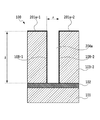
- FIG. 2 is a schematic explanatory diagram for explaining a case where a SiO 2 film is provided on the surface of the micro-vacuum wall before introducing the processing liquid into the micro-vacuum and processing the micro-vacuum.
- FIG. 3 is a schematic configuration diagram for explaining an example of a suitable manufacturing system for embodying the present invention.
- FIG. 4 is a schematic configuration diagram of a part of the production line shown in FIG. 3.
- FIG. 4 is a schematic configuration diagram of a part of the production line shown in FIG. 3.
- FIG. 5 is a schematic explanatory diagram for explaining a preferred configuration of a processing (medicine) liquid supply system provided inside the cartridge case 302.
- FIG. 6 is a schematic configuration diagram of the vacuum waste liquid collector 207.
- FIG. 7 is a schematic configuration diagram for explaining another preferable processing chamber.
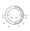
- FIG. 8 is a schematic top view for explaining the arrangement and ejection direction of nitrogen (N 2 ) gas ejection ports provided on the inner wall surface of the processing chamber 501 in FIG.
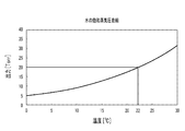
- FIG. 9 is a graph showing a saturated vapor pressure curve of water.
- FIG. 1 is a schematic explanatory diagram for explaining a situation in which bubbles exist in a narrow and deep hole (hole) provided in an SOI substrate and the processing liquid does not penetrate to the bottom of the hole.
- reference numeral 100 is an SOI substrate
- 101 is a Si (silicon) semiconductor substrate
- 102 is a SiO 2 (silicon oxide) layer
- 103 is a Si layer (103-1, 103-2)
- 104 is a hole
- 105 is a bubble.
- 106 is a treatment liquid
- 107 is a gas-liquid interface
- 108 is an inner wall surface (108-1, 108-2)
- 109 is an inner bottom wall surface
- 110 is an opening.
- the so-called aspect ratio is represented by “l / r”.
- the conditions under which the bubbles 105 are formed in the holes 104 are the surface tension, viscosity, liquid composition, surface smoothness of the side wall surface 108, wettability of the processing liquid used, and the size and aspect of “r” and “l”. There are many parameters such as ratio, and it is difficult to discuss them in general.
- the inventors first formed various holes in the SOI substrate 100 having a structural material as shown in FIG. 1 without limiting the inner structure of the hole 104 to a cylinder, and used ultrapure water as a treatment liquid to remove bubbles. I verified the formation tendency.
- the inner structure of the hole 104 is not limited to a cylindrical shape, but is a purse shape (the lower part of the opening extends in a bag shape or a tapered shape), a rectangular shape (a square shape such as a square, rectangle, or rhombus opening), a triangular shape It was created in various sizes as hexagonal, elliptical, super-elliptical, and star-shaped.
- the SiO 2 layer 102 constituting the inner bottom wall surface 109 was etched using hydrofluoric acid (HF) and buffered hydrofluoric acid (BFH) instead of ultrapure water.
- HF hydrofluoric acid
- BHF buffered hydrofluoric acid
- the present inventors have conducted intensive studies and as a result, the same SiO 2 film and the SiO 2 layer 102 to etching or cleaning of the hole bottom surface, by forming the hole-side surface constitutes an inner wall surface of the hole of the same material Further, it has been found that if a chemical solution having excellent wettability with respect to SiO 2 is used as a processing solution used for etching or cleaning, the inner wall surface of the hole can be efficiently processed even with a high aspect ratio hole.
- the inner space of the hall may be hereinafter referred to as “micro vacancy”.
- the value of “r” in the case of a structure in which the micro vacancy is not a cylinder is determined from the non-cylindrical “S” by regarding the micro vacancy as a cylinder.
- “l” is a depth (maximum depth) from the position of the opening to the position of the inner wall surface of the back of the micro-vacancy.
- the effect of reduced pressure in the present invention is that the aspect ratio (l / r) is 5 or more, or the aspect ratio is less than 5, and V / S (V: volume of micro-vacancy, S: area of opening) is 3 or more. Become noticeable in the case.
- the treatment liquid is buffered hydrofluoric acid and the object to be treated is an SOI substrate, a more remarkable effect can be obtained.
- FIG. 2 is a schematic explanatory diagram for explaining a case where an SiO 2 film is provided on the surface of the micro-vacuum wall before introducing the processing liquid into the micro-vacuum and processing the micro-vacuum.
- the same reference numerals are assigned to the same reference numerals in FIG.
- a predetermined hole is provided in advance on the Si layer 103, and then a chemical containing ozone for forming the SiO 2 film is introduced into the hole in a liquid state, in a spray state, or in a gaseous state.
- SiO 2 films 201a are formed on the inner wall surface 108 (108-1, 108-2) and the surface of the Si layer 103 by exposing the space in the hole to the environment including ) 204.
- Use of ozone water is preferable for the formation of an environment containing ozone.
- ozone may be introduced directly into the hole in a gaseous state.
- these acids may be used by mixing at least one selected from hydrogen peroxide, phosphoric acid, acetic acid, propionic acid, oxalic acid, and succinic acid.
- BHF is an aqueous solution in which 40% ammonium fluoride (NH 4 F) and 50% hydrofluoric acid are mixed at an arbitrary ratio.
- the processing liquid used for cleaning the inside of the micro vacant chamber 204a or etching the bottom SiO 2 layer 102 is selected from materials having a liquid composition excellent in affinity for SiO 2 .
- processing solutions include etching solutions such as hydrofluoric acid (HF) acid and buffered hydrofluoric acid (BHF), H 2 SO 4 / H 2 O 2 (SPM), NH 4 OH / H 2 O.
- cleaning liquid examples include 2 / H 2 O (APM), HCl / H 2 O 2 / H 2 O (HPM), and HF / H 2 O (DHF).
- An etching solution for forming the micro vacancy 204a in the Si layer 103 by etching is appropriately selected as desired.
- alkaline etching solution (1) one or more alkali compounds selected from tetramethylammonium hydroxide, potassium hydroxide, and sodium hydroxide, tetramethylammonium hydrochloride, tetramethylammonium nitrate, tetramethylammonium Alkali which is at least one selected from sulfate, tetramethylammonium acetate, tetramethylammonium propionate, tetramethylammonium oxalate, tetramethylammonium succinate, potassium chloride, sodium chloride, potassium acetate, sodium acetate
- An etching solution in which at least one salt-containing alkaline aqueous solution and hydroxylamine are mixed may be mentioned.
- the acidic etching solution examples include at least one acid selected from hydrochloric acid, sulfuric acid, nitric acid, phosphoric acid, acetic acid, propionic acid, oxalic acid, and succinic acid, hydrofluoric acid (H 2 SiF 6 ), and borofluoride. Selected from hydrofluoric acid (HBF 4 ), sodium fluoride (NaF), potassium fluoride (KF), calcium fluoride (CaF), ammonium fluoride (NH 4 F), acidic ammonium fluoride (NH 4 HF 2 ) An etching solution obtained by mixing at least one selected from the above can be used. In addition, hydrofluoric acid is also used.
- hydrofluoric acid is also used.
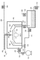
- FIG. 3 is a schematic configuration diagram for explaining an example of a suitable manufacturing system for embodying the present invention.
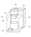
- FIG. 4 is a schematic configuration diagram of a part of the production line shown in FIG. In the manufacturing system shown in FIGS. 3 and 4, the treatment can be performed not only at normal pressure but also under reduced pressure as required.
- reference numeral 200 denotes a processing system
- 201 denotes a decompression processing chamber (chamber)
- 202 denotes a target object installation table
- 202-1 denotes a rotating shaft for the target object installation table
- 203 denotes a target object
- 204 Is an atmosphere gas supply line
- 205 is a processing (chemical) liquid supply line
- 206 is a recovery hood
- 207 is a vacuum waste liquid tank
- 208 is an air or N 2 supply line
- 209 is a drainage line
- 210 is a recovery line
- 211,212 Is an exhaust line
- 213 is an exhaust pump
- 214 to 221 are valve
- 222 is a supply amount variable nozzle for processing liquid
- 301 is a spinner
- 302 is a cartridge case
- 303 is an aluminum frame.
- the processing system 200 includes a processing chamber 201 that can be depressurized, and a waste liquid tank 207 that can be depressurized, and the inside thereof is configured to be depressurized to a predetermined value by an exhaust pump 213 as necessary. Yes.
- an atmospheric gas such as N 2 is supplied from the outside through the atmospheric gas supply line 204, and a processing (chemical) liquid is supplied from the outside through the processing liquid supply line 205 with a predetermined timing and a predetermined amount. Will be supplied respectively.
- an open / close valve 214 having a flow rate adjusting function is provided in the middle of the atmospheric gas supply line 204.
- a supply amount variable nozzle 224 is provided at the tip of the ozone-based processing liquid supply line 223 so that the processing liquid can be injected into the processing chamber 201 at a flow rate adjusted in a predetermined manner.
- a processing object installation table 202 is fixed and installed on a rotating shaft body 201-1 for the processing object installation table.
- a target object 203 is installed on the target object installation table 202.
- the atmospheric gas supplied into the reduced pressure processing chamber 201 via the atmospheric gas supply line 204 is indicated by an arrow B
- the treatment supplied via the recovery liquid 206 via the treatment liquid supply line 205 is indicated by an arrow B, as indicated by an arrow A.
- the liquid is collected from the collection line 210 into the waste liquid tank 207 through the collection hood 206.
- An opening / closing valve 217 is provided in the middle of the recovery line 210.
- a supply line 208 and an exhaust line 211 are coupled to the waste liquid tank 207.
- Supply line 208 is a supply line for atmospheric or N 2.
- the waste liquid 223 in the waste liquid tank 207 is discharged out of the waste liquid tank 207 through the drain line 209.
- the waste liquid tank 207 can be returned to atmospheric pressure by supplying air or N 2 from the supply line 208 as necessary.
- An open / close valve 215 is provided in the supply line 208.
- An opening / closing valve 216 is provided in the middle of the drain line 209.
- the processing chamber 201 is depressurized by the pump 213 as needed via the exhaust line 212 and the waste liquid tank 207 via the exhaust line 211, respectively.
- Valves 218 and 219 are installed in the middle of the exhaust line 211, and valves 220 and 221 are installed in the middle of the exhaust line 212, respectively.
- the valves 219 and 221 are open / close valves provided with a flow rate variable mechanism.
- the exhaust pump 213 is a moisture-resistant pump.
- a diaphragm type chemical dry vacuum pump specifically, DTC-120 (manufactured by ULVAC) is preferably employed.
- the processing chamber 201 and the waste liquid tank 207 are attached to, for example, an aluminum frame 303 as shown in FIG.
- a spinner 301 provided for rotating the rotary shaft 202-1 is also attached to the frame 303.
- a chemical basket 302 in which processing liquid is stored is connected to the upstream end of the processing (chemical) liquid supply line 205.
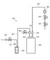
- FIG. 5 is a schematic explanatory diagram for explaining a preferred configuration of a processing (medicine) solution supply system provided inside the cartridge case 302.
- 400 is a nitrogen pressure feed process (chemical) liquid supply system
- 401 is a canister
- 402 is a process liquid supply line
- 403 and 411 are stop valves
- 404 is a flow control valve
- 405 is a flow meter
- 406 is a mist trap.
- 407 and 408 are nitrogen gas supply lines
- 409 is a vent (exhaust) valve
- 410 is a shunt joint
- 412 is a regulator
- 413 is a joint
- 414 and 415 are quick connectors.
- a processing (chemical) supply system 400 using a nitrogen pressure feeding system has a processing liquid supply line 402 in which a canister 401 is provided with a 3/8 inch line on the upstream side and a 1/4 inch line on the downstream side via a joint 413. Are connected to each other via a quick connector 414 and a 1/4 inch nitrogen gas supply line 407 via a quick connector 415.
- a stop valve 403, a flow rate adjustment valve 404, and a flow meter 405 are provided in the middle of the processing liquid supply line 402, a stop valve 403, a flow rate adjustment valve 404, and a flow meter 405 are provided.
- the downstream portion of the processing liquid supply line 402 on the stop valve 403 side is connected to the processing liquid supply line 205.
- a vent (exhaust) valve 409 and a diversion joint 410 are provided in the middle of the nitrogen gas supply line 407.
- the vent (exhaust) valve 409 is for exhausting the nitrogen gas in the canister 401 and the nitrogen gas supply line 407 to the outside.
- the downstream side of the nitrogen gas supply line 407 is inserted into the mist trap 406.
- Nitrogen gas is introduced into the mist trap 406 through the regulator 412, the stop valve 411, and the nitrogen gas supply line 408.
- the mist trap 406 is provided to prevent the processing liquid from flowing back to the upstream side.
- FIG. 6 is a schematic configuration diagram of the waste liquid tank 207.
- 501 is a drain flange
- 502 is a decompression flange
- 503 is a waste liquid introduction flange
- 504 is a gas introduction flange
- 505 is a vacuum gauge
- 506 is a flow meter
- 507 is a liquid level. An observation window is shown.
- the waste liquid tank 207 includes a drain line 209 through a drain flange 501, a drain line 211 through a decompression flange 502, a recovery line 210 through a waste liquid introduction flange 503, and a flange 504.
- a supply line 208 is connected via The vacuum gauge 505 measures the pressure in the waste liquid tank 207.
- a liquid level observation window 504 made of a transparent member for waste liquid is provided in order to observe the water level of the waste liquid in the waste liquid tank 207.
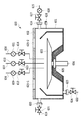
- FIG. 7 is a schematic configuration diagram for explaining another suitable processing chamber.
- 600 is a decompression processing chamber
- 601 is a chamber structure
- 602 is an upper lid
- 603 is a stage for installing a target object
- 604 is a rotating shaft body
- 605 is a magnetic fluid seal
- 606 is a special processing (medicine) solution.
- 607 is ozone water supply line
- 608 is ultrapure water supply line
- 609, 610, 611 and 618 are flowmeters
- 612, 613, 614, 617, 621 and 624 are valves
- 615 is a gas introduction line
- 616, 620 and 623 are flanges
- 622 is a waste liquid line
- 625 is an observation window (625-1 and 625-2)
- 626 is a vacuum gauge.
- a supply line. The rest is basically the same as the processing chamber 201 except for another different point.
- a gas introduction line 615 and a gas discharge line 619 are attached to the processing chamber 600.
- An atmospheric gas in the processing chamber 600 is introduced through the gas introduction line 615.
- the gas introduction line 615 is attached to the processing chamber 600 by a flange 616.
- An opening / closing valve 617 and a flow meter 618 are provided in the middle of the gas introduction line 615.
- the gas discharge line 619 is attached to the processing chamber 600 by a flange 620.
- An opening / closing valve 621 is provided in the middle of the gas discharge line 615.
- a downstream side of the gas discharge line 615 is connected to a pump (not shown) similar to the vacuum pump 213.
- the processing chamber 600 is configured such that the inside is maintained in a reduced pressure state by the chamber structure 601 and the upper lid 602.
- the upper lid 602 is provided with two observation windows 625-1 and 625-2 for observing the inside of the chamber 600.
- a stage 603 for installing a target object on which the target object is set is provided inside the processing chamber 600.
- a rotating shaft 604 for rotating the stage 603 is fixed to the stage 603 in a removable state.
- the rotating shaft body 604 is sealed with a magnetic fluid seal 605 and joined to a rotating shaft body of a spinner installed outside the decompression processing chamber 600.
- a flow meter 609 and a valve 612 are provided in the middle of the special processing (chemical) liquid supply line 606.
- a flow meter 610 and a valve 613 are provided in the middle of the ozone water supply line 607.
- a flow meter 611 and a valve 614 are provided in the middle of the ultrapure water supply line 608.
- a waste liquid line 622 is attached to the vacuum processing chamber 600 by a flange 623 at the bottom of the vacuum processing chamber 600.
- An opening / closing valve 624 is provided in the middle of the waste liquid line 622.
- a vacuum gauge 626 for measuring the pressure in the processing chamber 600 is attached to the side surface of the decompression processing chamber 600.
- a gas ejection inner wall pipe 701 coupled to the gas introduction line 615 is attached to the inner wall of the processing chamber 600 capable of depressurization.
- the gas ejection inner wall pipe 701 is provided with a predetermined number of gas ejection ports 702 whose ejection direction is directed to the central axis of the inner space of the processing chamber 600.
- the ejection diameter and the number of the gas ejection ports 702 are designed to be a predetermined gas ejection flow rate.
- the gas jetting (blowing) flow rate from the gas jetting port 702 is determined in advance at the time of design so as not to cause a stirring action or a turbulent action in the processing chamber as much as possible by the gas jetting. It is desirable to determine the optimum value in the preliminary experiment of gas ejection.
- the degree of stirring action or turbulent action due to gas ejection depends on the gas exhaust speed, and is preferably 0.1 to 5.0 m / sec, more preferably 0.5 to 3.0 m in the present invention. / sec, optimally around 2.0 m / sec.
- N 2 gas For example, when 20 nozzle holes 702 having a diameter of 2 mm are provided on the semicircular circumference as shown in the figure, it is desirable to flow N 2 gas into the processing chamber 600 at an amount of 200 cc / min.
- the flow rate of N 2 gas at this time is 2.0 m / sec.
- the treatment liquid is sufficiently deaerated beforehand in order to enhance the gas absorption ability.
- N 2 gas or atmospheric gas has been exemplified as the atmospheric gas.
- CO 2 gas is used instead of these gases, the amount dissolved in the treatment liquid can be reduced. Since it can increase, it is preferable.
- FIG. 9 is a graph showing a saturated vapor pressure curve of water.
- the horizontal axis indicates temperature (° C.), and the vertical axis indicates pressure (Torr).
- the degree of the pressure reduction is preferably set to 30 Torr as an upper limit in order to avoid boiling of the processing liquid. If pressure is applied after supplying the treatment liquid onto the surface of the substrate to be treated under reduced pressure, even if bubbles remain in the tail hole, it is desirable because the volume of the bubble is reduced by pressurization and easily escapes from the hole. For example, when the pressure is reduced from 30 Torr to 760 Torr, the volume of the bubbles becomes about 1/25.
- the present invention it is also a preferable aspect to reduce the pressure and supply the treatment liquid sufficiently and then pressurize. Furthermore, this pressure reduction and pressurization may be repeated.
- the treatment is usually carried out under normal pressure, but the effect is further enhanced when carried out under reduced pressure as described above.
- a treatment chamber capable of depressurization as described above was prepared, and the process was performed under reduced pressure (30 Torr). As a result, both the aqueous hydrofluoric acid solution (FH 1-20%) and buffered hydrofluoric acid (ammonium fluoride: 20%, HF: 1-20%) were completely etched at a rate of 100%.
- a treatment liquid having improved wettability to SiO 2 for example, BHF-added surfactant
- a CO 2 atmosphere for example, CO 2 atmosphere.
- Two 5-inch SOI substrates were prepared. In the semiconductor field, holes (micro vacancies) having a size that falls within the numerical range described in the description of the present invention but having a different size such as depth are generally formed in the Si layer on the surface of each substrate. 500 samples (Samples A and B) were produced by the etching process. The hole pattern and each hole size were devised so that the samples A and B would be the same.
- Samples A and B were processed as follows using the apparatus shown in FIG. Sample A was rotated at 400 rpm, and 5 ppm concentration ozone water was supplied from the center at a flow rate of 1 L / min for 1 min for processing. Thereafter, the sample wafer was idled and dried at 1200 rpm for 1 min (pretreatment). Thereafter, the sample A pretreated as described above was rotated at 400 rpm, and BHF was supplied from the center at a flow rate of 1 L / min for 5 min for processing. Next, rinsing was performed by supplying ultrapure water for 5 minutes at a rotation speed of 400 rpm and a flow rate of 2 L / min from the center.
- sample A was idled at 1200 rpm for 1 min and dried (etching process).
- Sample B was subjected to the same treatment as Sample A except that the above pretreatment was not performed. After the above procedure was completed, the defective etching of the sample hole (micro-vacancy) was evaluated. In the case of Sample A that was etched after the pretreatment, the number of defectives was 0 out of 500. On the other hand, in the case of Sample B that was etched without pretreatment, the number of defective etchings was 85 out of 500.
- the technology of the present invention is not limited to TSV, and can be applied to technical fields such as MEMS as long as it requires a high aspect ratio hole. .
- 606 Special treatment (chemical) liquid supply line 607 ... Ozone water supply line 608 ... Ultrapure water supply line 609, 610, 611, 618 ... Flowmeters 612, 613, 614, 617, 621 , 624 ... Valve 615 ... Gas introduction line 619 ... Gas discharge line 616, 620, 623 ... Flange 622 ... Waste liquid line 625 ... Observation window (625-1, 625-2) ) 626 ... Vacuum gauge 701 ... Gas ejection inner wall tube 702 ... Gas ejection port
Landscapes
- Cleaning Or Drying Semiconductors (AREA)
- Chemical & Material Sciences (AREA)
- Chemical Kinetics & Catalysis (AREA)
- General Chemical & Material Sciences (AREA)
- Weting (AREA)
- Cleaning By Liquid Or Steam (AREA)
Abstract
Description
本発明において超音波振動を仮に採用するとしても、パターン崩れが起こらない程度の範囲で超音波振動を穏やかにするのが望ましい。
[実施例]
5インチSOI基体を2枚用意した。
各基体の表面にあるSi層に、本発明の説明の中に記載した数値範囲に入るサイズであるが、深さなどのサイズは異なるホール(マイクロ空室)を、半導体分野で一般に行われているエッチングプロセスで、500個作成した(試料A、B)。
ホールパターン、各ホールサイズは、試料A、Bで同じになるように工夫した。
この試料A、Bを図7の装置を用いて以下の様に処理した。試料Aを400rpmで回転させ、5ppmの濃度オゾン水を中心より流量1L/minで1min間供給して処理を行った。その後1200rpmで1min間、試料ウェーハを空回転させ乾燥した(事前処理)。 その後、上記の様に事前処理した試料Aを400rpmで回転させ、BHFを中心より流量1L/minで5min間供給して処理を行った。次いで、回転数400rpmで、中心より流量2L/minとして超純水を5min間供給してリンス処理をした。その後1200rpmで1min間試料Aを空回転させ乾燥した(エッチング処理)。
試料Bは、上記の事前処理を行わない以外は、試料Aと同様の処理を施した。
上記の手順終了後、試料のホール(マイクロ空室)のエッチング不良を評価したところ、事前処理の後にエッチング処理をした試料Aの場合は、不良は、500個中0個だった。
それに対して事前処理をせずにエッチング処理を行った試料Bの場合は、エッチング不良は、500個中85個にもなった。
101・・・Si(シリコン)半導体基板
102・・・SiO2(酸化シリコン)層
103・・・Si層(103-1,103-2)
104・・・ホール
105・・・気泡
106・・・処理液
107・・・気液界面
108・・・内側壁面(108-1,108-2)
109・・・内底壁面
110・・・開口
200・・・処理システム
201・・・減圧処理チャンバー(室)
201a・・・酸化シリコン膜(201a-1、201a-2)
202・・・被処理体設置テーブル
202-1・・・被処理体設置テーブル用の回転軸体
203・・・被処理体
204・・・雰囲気ガス供給ライン
204a・・・マイクロ室
205・・・処理(薬)液供給ライン
206・・・回収フード
207・・・減圧廃液タンク
208・・・大気若しくはN2供給ライン
209・・・排液ライン
210・・・回収ライン
211、212・・・排気ライン
213・・・排気ポンプ
214、215,216,217,218,219,220、221・・・バルブ
222・・・処理液用の供給量可変ノズル
223・・・オゾン系処理液供給ライン
224・・・オゾン系処理液用の供給量可変ノズル
301・・・スピナー
302・・・薬莢
303・・・アルミフレーム
400・・・窒素圧送方式処理(薬)液供給系
401・・・キャニスター
402・・・処理液供給ライン
403、411・・・ストップバルブ
404・・・流量調節バルブ
405・・・流量計
406・・・ミストトラップ
407、408・・・窒素ガス供給ライン
409・・・ベント(排気)バルブ
410・・・分流継手
412・・・レギュレーター
413・・・継手
414、415・・・クイックコネクター
501・・・ドレイン用のフランジ
502・・・減圧用のフランジ
503・・・廃液導入用のフランジ
504・・・ガス導入用のフランジ
505・・・真空計
506・・・流量計
507・・・液位観察用窓
600・・・減圧処理チャンバー
601・・・チャンバー構成体
602・・・上蓋
603・・・被処理体設置用のステージ
604・・・回転軸体
605・・・磁性流体シール
606・・・特殊処理(薬)液供給ライン
607・・・オゾン水供給ライン
608・・・超純水供給ライン
609,610,611,618・・・流量計
612,613,614、617、621,624・・・バルブ
615・・・ガス導入ライン
619・・・ガス排出ライン
616、620、623・・・フランジ
622・・・廃液ライン
625・・・観察用窓(625-1,625-2)
626・・・真空計
701・・・ガス噴出内壁管
702・・・ガス噴出口
Claims (1)
- 酸化シリコン層と該層上にシリコン層が積層されている基体であって、該シリコン層は、処理液が付与される表面と該表面に開口を有し該シリコン層を貫通し底部に前記酸化シリコン層の表面が露出しているマイクロ空室を内部に有し、且つ該マイクロ空室のアスペクト比(l/r)が5以上かまたはアスペクト比が5未満でかつV/S(V: マイクロ空室の容積、S:開口の面積)が3以上である基体が設置されている処理空間において、前記開口を通じて前記マイクロ空室を酸化シリコン膜形成の室内処理環境に晒して前記マイクロ空室の内壁表面に酸化シリコン膜を形成し、次いで、酸化シリコンに対して濡れ性のある処理液を内壁に酸化シリコン膜が形成されたマイクロ空室の空間に導入して内壁面処理を行うことを特徴とするマイクロ空室の内壁面処理方法。
Priority Applications (3)
| Application Number | Priority Date | Filing Date | Title |
|---|---|---|---|
| US14/891,020 US10020222B2 (en) | 2013-05-15 | 2013-05-15 | Method for processing an inner wall surface of a micro vacancy |
| PCT/JP2013/003108 WO2014184825A1 (ja) | 2013-05-15 | 2013-05-15 | マイクロ空室の内壁面処理方法 |
| JP2013549461A JP5569831B1 (ja) | 2013-05-15 | 2013-05-15 | マイクロ空室の内壁面処理方法 |
Applications Claiming Priority (1)
| Application Number | Priority Date | Filing Date | Title |
|---|---|---|---|
| PCT/JP2013/003108 WO2014184825A1 (ja) | 2013-05-15 | 2013-05-15 | マイクロ空室の内壁面処理方法 |
Publications (1)
| Publication Number | Publication Date |
|---|---|
| WO2014184825A1 true WO2014184825A1 (ja) | 2014-11-20 |
Family
ID=51427249
Family Applications (1)
| Application Number | Title | Priority Date | Filing Date |
|---|---|---|---|
| PCT/JP2013/003108 Ceased WO2014184825A1 (ja) | 2013-05-15 | 2013-05-15 | マイクロ空室の内壁面処理方法 |
Country Status (3)
| Country | Link |
|---|---|
| US (1) | US10020222B2 (ja) |
| JP (1) | JP5569831B1 (ja) |
| WO (1) | WO2014184825A1 (ja) |
Families Citing this family (4)
| Publication number | Priority date | Publication date | Assignee | Title |
|---|---|---|---|---|
| JP6875811B2 (ja) * | 2016-09-16 | 2021-05-26 | 株式会社Screenホールディングス | パターン倒壊回復方法、基板処理方法および基板処理装置 |
| US10737359B2 (en) * | 2018-04-09 | 2020-08-11 | Lam Research Corporation | Manufacture of an orifice plate for use in gas calibration |
| CN113394074A (zh) * | 2020-03-11 | 2021-09-14 | 长鑫存储技术有限公司 | 半导体结构的处理方法 |
| KR102726738B1 (ko) * | 2022-12-14 | 2024-11-07 | 세메스 주식회사 | 처리액 배출 어셈블리 및 처리액 배출 방법 |
Citations (4)
| Publication number | Priority date | Publication date | Assignee | Title |
|---|---|---|---|---|
| JPH1187290A (ja) * | 1997-09-10 | 1999-03-30 | Hitachi Ltd | 半導体基板の洗浄方法及びそれを用いた半導体装置の製造方法 |
| JP2003077899A (ja) * | 2001-09-04 | 2003-03-14 | Sharp Corp | 半導体基板の洗浄方法 |
| WO2012096133A1 (ja) * | 2011-01-12 | 2012-07-19 | セントラル硝子株式会社 | 保護膜形成用薬液 |
| JP2012156369A (ja) * | 2011-01-27 | 2012-08-16 | Napura:Kk | 回路基板、電子デバイス及びその製造方法 |
Family Cites Families (62)
| Publication number | Priority date | Publication date | Assignee | Title |
|---|---|---|---|---|
| US4471040A (en) | 1980-09-10 | 1984-09-11 | Canon Kabushiki Kaisha | Electrophotographic disazo photosensitive member |
| GB2088074B (en) | 1980-09-26 | 1984-12-19 | Copyer Co | Electrophotographic photosensitive member |
| US4390611A (en) | 1980-09-26 | 1983-06-28 | Shozo Ishikawa | Electrophotographic photosensitive azo pigment containing members |
| US4399206A (en) | 1980-10-06 | 1983-08-16 | Canon Kabushiki Kaisha | Disazo electrophotographic photosensitive member |
| US4399208A (en) | 1980-11-22 | 1983-08-16 | Canon Kabushiki Kaisha | Electrophotographic photosensitive member |
| US4420548A (en) | 1980-11-28 | 1983-12-13 | Canon Kabushiki Kaisha | Electrophotographic member with hydrazone or ketazine compounds |
| JPS5799648A (en) | 1980-12-13 | 1982-06-21 | Copyer Co Ltd | Electrophotographic receptor |
| US4446217A (en) | 1981-02-03 | 1984-05-01 | Canon Kabushiki Kaisha | Electrophotographic photosensitive member having a hydrazone containing layer |
| US4418133A (en) | 1981-03-27 | 1983-11-29 | Canon Kabushiki Kaisha | Disazo photoconductive material and electrophotographic photosensitive member having disazo pigment layer |
| JPS57195255A (en) | 1981-05-26 | 1982-11-30 | Canon Inc | Electrophotographic receptor |
| US4427753A (en) | 1981-06-02 | 1984-01-24 | Canon Kabushiki Kaisha | Electrophotographic photosensitive member with disazo or trisazo compound |
| US4454211A (en) | 1981-06-10 | 1984-06-12 | Canon Kabushiki Kaisha | Electrophotographic photosensitive member with pyrazoline charge transport material |
| US4551404A (en) | 1981-06-18 | 1985-11-05 | Canon Kabushiki Kaisha | Disazo electrophotographic photosensitive member |
| JPS5816243A (ja) | 1981-07-22 | 1983-01-29 | Copyer Co Ltd | 電子写真感光体 |
| US4399207A (en) | 1981-07-31 | 1983-08-16 | Canon Kabushiki Kaisha | Electrophotographic photosensitive member with hydrazone compound |
| US4456671A (en) | 1981-12-23 | 1984-06-26 | Canon Kabushiki Kaisha | Electrophotographic photosensitive member having a photosensitive layer containing a hydrazone compound |
| JPS58199353A (ja) | 1982-05-17 | 1983-11-19 | Canon Inc | 電子写真感光体 |
| US4495264A (en) | 1983-03-15 | 1985-01-22 | Canon Kabushiki Kaisha | Electrophotographic photosensitive member comprising disazo compound |
| JPS59204839A (ja) | 1983-05-09 | 1984-11-20 | Canon Inc | 電子写真感光体 |
| JPS61151547A (ja) | 1984-12-26 | 1986-07-10 | Canon Inc | 電子写真感光体 |
| US4743523A (en) | 1985-04-02 | 1988-05-10 | Canon Kabushiki Kaisha | Photosensitive member for electrophotography |
| US4735882A (en) | 1985-04-02 | 1988-04-05 | Canon Kabushiki Kaisha | Trisazo photsensitive member for electrophotography |
| US4666810A (en) | 1985-04-17 | 1987-05-19 | Canon Kabushiki Kaisha | Photosensitive member for electrophotography comprising azo pigments |
| US4760003A (en) | 1985-05-24 | 1988-07-26 | Canon Kabushiki Kaisha | Electrophotographic photosensitive member containing disazo compound |
| JPS61272754A (ja) | 1985-05-29 | 1986-12-03 | Canon Inc | 電子写真感光体 |
| JPH0693501B2 (ja) * | 1985-10-31 | 1994-11-16 | 日本電気株式会社 | 半導体集積回路 |
| JPS62147462A (ja) | 1985-12-20 | 1987-07-01 | Canon Inc | 電子写真感光体 |
| JPH0795541B2 (ja) * | 1986-07-02 | 1995-10-11 | 松下電器産業株式会社 | 処理方法 |
| US4931371A (en) | 1987-11-24 | 1990-06-05 | Canon Kabushiki Kaisha | Electrophotographic photosensitive member |
| JPH0212598A (ja) | 1988-06-30 | 1990-01-17 | Toshiba Corp | 携帯可能電子装置 |
| JPH07105438B2 (ja) * | 1993-01-05 | 1995-11-13 | 日本電気株式会社 | 半導体装置の製造方法 |
| JPH08264500A (ja) * | 1995-03-27 | 1996-10-11 | Sony Corp | 基板の洗浄方法 |
| JP3274389B2 (ja) * | 1996-08-12 | 2002-04-15 | 株式会社東芝 | 半導体基板の洗浄方法 |
| JP3488030B2 (ja) | 1996-12-05 | 2004-01-19 | 森田化学工業株式会社 | 半導体装置の製造方法 |
| US6245691B1 (en) * | 1998-05-29 | 2001-06-12 | Taiwan Semiconductor Manufacturing Company | Ozone-teos method for forming with attenuated surface sensitivity a silicon oxide dielectric layer upon a thermally oxidized silicon substrate layer |
| US6432324B1 (en) | 1999-08-25 | 2002-08-13 | Canon Kasei Kabushiki Kaisha | Semiconducting member, functional member for electrophotography, and process cartridge |
| JP2002289575A (ja) | 2001-03-28 | 2002-10-04 | Dainippon Screen Mfg Co Ltd | 基板処理方法及びその装置 |
| JP3967108B2 (ja) * | 2001-10-26 | 2007-08-29 | 富士通株式会社 | 半導体装置およびその製造方法 |
| JP3604018B2 (ja) * | 2002-05-24 | 2004-12-22 | 独立行政法人科学技術振興機構 | シリコン基材表面の二酸化シリコン膜形成方法、半導体基材表面の酸化膜形成方法、及び半導体装置の製造方法 |
| JP4356109B2 (ja) * | 2004-01-23 | 2009-11-04 | 学校法人早稲田大学 | マイクロリアクタの製造方法 |
| JP2006278955A (ja) | 2005-03-30 | 2006-10-12 | Dainippon Screen Mfg Co Ltd | 基板処理方法および基板処理装置 |
| US7437820B2 (en) * | 2006-05-11 | 2008-10-21 | Eastman Kodak Company | Method of manufacturing a charge plate and orifice plate for continuous ink jet printers |
| WO2009011303A1 (ja) * | 2007-07-13 | 2009-01-22 | Canon Anelva Corporation | Si層凝集抑制方法、半導体装置の製造方法及び真空処理装置 |
| JP5025508B2 (ja) | 2008-01-30 | 2012-09-12 | 東京エレクトロン株式会社 | ポリシリコン膜の除去方法および記憶媒体 |
| JP5195102B2 (ja) | 2008-07-11 | 2013-05-08 | 大日本印刷株式会社 | センサおよびその製造方法 |
| US7935571B2 (en) * | 2008-11-25 | 2011-05-03 | Freescale Semiconductor, Inc. | Through substrate vias for back-side interconnections on very thin semiconductor wafers |
| JP5286052B2 (ja) * | 2008-11-28 | 2013-09-11 | 株式会社東芝 | 半導体装置及びその製造方法 |
| US8168470B2 (en) * | 2008-12-08 | 2012-05-01 | Stats Chippac, Ltd. | Semiconductor device and method of forming vertical interconnect structure in substrate for IPD and baseband circuit separated by high-resistivity molding compound |
| JP5201048B2 (ja) * | 2009-03-25 | 2013-06-05 | 富士通株式会社 | 半導体装置とその製造方法 |
| US8614053B2 (en) | 2009-03-27 | 2013-12-24 | Eastman Chemical Company | Processess and compositions for removing substances from substrates |
| US8278187B2 (en) * | 2009-06-24 | 2012-10-02 | Semiconductor Energy Laboratory Co., Ltd. | Method for reprocessing semiconductor substrate by stepwise etching with at least two etching treatments |
| JP2011159885A (ja) * | 2010-02-02 | 2011-08-18 | Toshiba Corp | 薄膜の製造方法 |
| US8154119B2 (en) * | 2010-03-31 | 2012-04-10 | Toyota Motor Engineering & Manufacturing North America, Inc. | Compliant spring interposer for wafer level three dimensional (3D) integration and method of manufacturing |
| CN106245073B (zh) * | 2010-05-19 | 2019-12-20 | 诺发系统有限公司 | 用金属电化学填充高纵横比的大型凹入特征的方法、水溶液电镀槽溶液、电镀设备以及系统 |
| KR101396271B1 (ko) | 2010-06-30 | 2014-05-16 | 샌트랄 글래스 컴퍼니 리미티드 | 웨이퍼의 세정방법 |
| CN102453915B (zh) | 2010-10-27 | 2014-03-12 | 富葵精密组件(深圳)有限公司 | 蚀刻装置及使用该蚀刻装置蚀刻基板的方法 |
| US9704793B2 (en) | 2011-01-04 | 2017-07-11 | Napra Co., Ltd. | Substrate for electronic device and electronic device |
| JP2012204424A (ja) | 2011-03-24 | 2012-10-22 | Toshiba Corp | 半導体基板の表面処理方法および基板処理装置 |
| US8872345B2 (en) * | 2011-07-07 | 2014-10-28 | Taiwan Semiconductor Manufacturing Company, Ltd. | Forming grounded through-silicon vias in a semiconductor substrate |
| US9117759B2 (en) * | 2011-08-10 | 2015-08-25 | Micron Technology, Inc. | Methods of forming bulb-shaped trenches in silicon |
| JP6021441B2 (ja) * | 2012-05-25 | 2016-11-09 | ラピスセミコンダクタ株式会社 | 半導体装置 |
| US20130334699A1 (en) * | 2012-06-19 | 2013-12-19 | Chien-Li Kuo | Semiconductor device and fabricating method thereof |
-
2013
- 2013-05-15 US US14/891,020 patent/US10020222B2/en not_active Expired - Fee Related
- 2013-05-15 WO PCT/JP2013/003108 patent/WO2014184825A1/ja not_active Ceased
- 2013-05-15 JP JP2013549461A patent/JP5569831B1/ja not_active Expired - Fee Related
Patent Citations (4)
| Publication number | Priority date | Publication date | Assignee | Title |
|---|---|---|---|---|
| JPH1187290A (ja) * | 1997-09-10 | 1999-03-30 | Hitachi Ltd | 半導体基板の洗浄方法及びそれを用いた半導体装置の製造方法 |
| JP2003077899A (ja) * | 2001-09-04 | 2003-03-14 | Sharp Corp | 半導体基板の洗浄方法 |
| WO2012096133A1 (ja) * | 2011-01-12 | 2012-07-19 | セントラル硝子株式会社 | 保護膜形成用薬液 |
| JP2012156369A (ja) * | 2011-01-27 | 2012-08-16 | Napura:Kk | 回路基板、電子デバイス及びその製造方法 |
Also Published As
| Publication number | Publication date |
|---|---|
| US10020222B2 (en) | 2018-07-10 |
| US20160086845A1 (en) | 2016-03-24 |
| JP5569831B1 (ja) | 2014-08-13 |
| JPWO2014184825A1 (ja) | 2017-02-23 |
Similar Documents
| Publication | Publication Date | Title |
|---|---|---|
| JP5549026B1 (ja) | マイクロ空室の内壁面処理方法 | |
| US20090014028A1 (en) | Method of cleaning substrates and substrate cleaner | |
| US9859111B2 (en) | Apparatus and method of treating surface of semiconductor substrate | |
| CN101452824B (zh) | 用于湿化学处理半导体晶片的方法 | |
| JP5569831B1 (ja) | マイクロ空室の内壁面処理方法 | |
| CN1276271A (zh) | 特超声清洗半导体晶片中的去离子水温控去气 | |
| JP7258915B2 (ja) | 半導体ウエハの洗浄に用いられる方法及び装置 | |
| JP2008182188A (ja) | 電子材料用洗浄液および洗浄方法 | |
| JP2011134864A (ja) | 洗浄方法 | |
| JP4482844B2 (ja) | ウェハの洗浄方法 | |
| JP6243802B2 (ja) | デバイスの製造方法 | |
| TW453904B (en) | Method for cleaning semiconductor wafer surface | |
| CN114361026A (zh) | 半导体结构及其形成方法和臭氧清洗设备 | |
| JP5561811B1 (ja) | エッチング方法及びlsiデバイスの製造方法、並びに3d集積化lsiデバイス製造方法 | |
| US20060065627A1 (en) | Processing electronic devices using a combination of supercritical fluid and sonic energy | |
| TWI610355B (zh) | 微空室之內壁面處理方法及元件之製造方法 | |
| TWI567810B (zh) | The method of making the inner wall surface of the micro chamber and the manufacturing method of the component | |
| US20020121286A1 (en) | Rinsing solution and rinsing and drying methods for the prevention of watermark formation on a surface | |
| JP7423980B2 (ja) | ウエハの表面の洗浄装置及びウエハの表面の洗浄方法 | |
| JP2014212299A (ja) | マイクロ空室の内壁面処理方法 | |
| JP2001054768A (ja) | 洗浄方法及び洗浄装置 | |
| JP6020626B2 (ja) | デバイス用Ge基板の洗浄方法、洗浄水供給装置及び洗浄装置 | |
| TWI487022B (zh) | Method of treating inner wall of fine pores | |
| JP2007273806A (ja) | 半導体基板の洗浄方法および洗浄装置 | |
| TW201600183A (zh) | 元件用Ge基板之洗淨方法,洗淨水供給裝置及洗淨裝置 |
Legal Events
| Date | Code | Title | Description |
|---|---|---|---|
| ENP | Entry into the national phase |
Ref document number: 2013549461 Country of ref document: JP Kind code of ref document: A |
|
| 121 | Ep: the epo has been informed by wipo that ep was designated in this application |
Ref document number: 13884621 Country of ref document: EP Kind code of ref document: A1 |
|
| WWE | Wipo information: entry into national phase |
Ref document number: 14891020 Country of ref document: US |
|
| NENP | Non-entry into the national phase |
Ref country code: DE |
|
| 122 | Ep: pct application non-entry in european phase |
Ref document number: 13884621 Country of ref document: EP Kind code of ref document: A1 |