WO2014148425A1 - 接合体の製造方法及びパワーモジュール用基板の製造方法 - Google Patents
接合体の製造方法及びパワーモジュール用基板の製造方法 Download PDFInfo
- Publication number
- WO2014148425A1 WO2014148425A1 PCT/JP2014/057121 JP2014057121W WO2014148425A1 WO 2014148425 A1 WO2014148425 A1 WO 2014148425A1 JP 2014057121 W JP2014057121 W JP 2014057121W WO 2014148425 A1 WO2014148425 A1 WO 2014148425A1
- Authority
- WO
- WIPO (PCT)
- Prior art keywords
- copper
- manufacturing
- ceramic substrate
- substrate
- power module
- Prior art date
Links
- 239000000758 substrate Substances 0.000 title claims abstract description 159
- 238000004519 manufacturing process Methods 0.000 title claims abstract description 64
- 238000000034 method Methods 0.000 title claims abstract description 32
- 239000000463 material Substances 0.000 claims abstract description 145
- 239000000919 ceramic Substances 0.000 claims abstract description 133
- RYGMFSIKBFXOCR-UHFFFAOYSA-N Copper Chemical compound [Cu] RYGMFSIKBFXOCR-UHFFFAOYSA-N 0.000 claims abstract description 119
- 239000010949 copper Substances 0.000 claims abstract description 116
- 229910052802 copper Inorganic materials 0.000 claims abstract description 115
- 239000000945 filler Substances 0.000 claims abstract description 68
- 239000007769 metal material Substances 0.000 claims abstract description 50
- 238000010438 heat treatment Methods 0.000 claims abstract description 45
- 238000002844 melting Methods 0.000 claims abstract description 18
- 230000008018 melting Effects 0.000 claims abstract description 18
- 229910052751 metal Inorganic materials 0.000 claims description 60
- 239000002184 metal Substances 0.000 claims description 60
- 238000005219 brazing Methods 0.000 claims description 55
- 229910000679 solder Inorganic materials 0.000 claims description 28
- 229910000881 Cu alloy Inorganic materials 0.000 claims description 16
- 229910052782 aluminium Inorganic materials 0.000 claims description 13
- XAGFODPZIPBFFR-UHFFFAOYSA-N aluminium Chemical compound [Al] XAGFODPZIPBFFR-UHFFFAOYSA-N 0.000 claims description 13
- 229910017888 Cu—P Inorganic materials 0.000 claims description 10
- 229910020938 Sn-Ni Inorganic materials 0.000 claims description 9
- 229910008937 Sn—Ni Inorganic materials 0.000 claims description 9
- 229910017755 Cu-Sn Inorganic materials 0.000 claims description 8
- 229910017927 Cu—Sn Inorganic materials 0.000 claims description 8
- KUNSUQLRTQLHQQ-UHFFFAOYSA-N copper tin Chemical compound [Cu].[Sn] KUNSUQLRTQLHQQ-UHFFFAOYSA-N 0.000 claims description 8
- 238000010030 laminating Methods 0.000 claims description 8
- 229910000838 Al alloy Inorganic materials 0.000 claims description 5
- 229910017767 Cu—Al Inorganic materials 0.000 claims description 3
- 238000003475 lamination Methods 0.000 abstract description 5
- 239000007791 liquid phase Substances 0.000 description 19
- 239000004065 semiconductor Substances 0.000 description 16
- 238000005304 joining Methods 0.000 description 15
- 229910017945 Cu—Ti Inorganic materials 0.000 description 10
- 238000009792 diffusion process Methods 0.000 description 9
- PMHQVHHXPFUNSP-UHFFFAOYSA-M copper(1+);methylsulfanylmethane;bromide Chemical compound Br[Cu].CSC PMHQVHHXPFUNSP-UHFFFAOYSA-M 0.000 description 8
- 239000007790 solid phase Substances 0.000 description 7
- 238000001816 cooling Methods 0.000 description 5
- 239000011888 foil Substances 0.000 description 5
- 229910018125 Al-Si Inorganic materials 0.000 description 4
- 229910018520 Al—Si Inorganic materials 0.000 description 4
- 229910004837 P—Sn Inorganic materials 0.000 description 3
- 239000000155 melt Substances 0.000 description 3
- 238000012360 testing method Methods 0.000 description 3
- 239000012809 cooling fluid Substances 0.000 description 2
- 238000001514 detection method Methods 0.000 description 2
- 238000011156 evaluation Methods 0.000 description 2
- 239000000289 melt material Substances 0.000 description 2
- 229910052759 nickel Inorganic materials 0.000 description 2
- 229910017944 Ag—Cu Inorganic materials 0.000 description 1
- 229910018072 Al 2 O 3 Inorganic materials 0.000 description 1
- 229910052581 Si3N4 Inorganic materials 0.000 description 1
- 229910020836 Sn-Ag Inorganic materials 0.000 description 1
- 229910020935 Sn-Sb Inorganic materials 0.000 description 1
- 229910020988 Sn—Ag Inorganic materials 0.000 description 1
- 229910018956 Sn—In Inorganic materials 0.000 description 1
- 229910008757 Sn—Sb Inorganic materials 0.000 description 1
- PNEYBMLMFCGWSK-UHFFFAOYSA-N aluminium oxide Inorganic materials [O-2].[O-2].[O-2].[Al+3].[Al+3] PNEYBMLMFCGWSK-UHFFFAOYSA-N 0.000 description 1
- 230000015572 biosynthetic process Effects 0.000 description 1
- 230000015556 catabolic process Effects 0.000 description 1
- 239000004020 conductor Substances 0.000 description 1
- 238000012790 confirmation Methods 0.000 description 1
- 238000006731 degradation reaction Methods 0.000 description 1
- 230000000694 effects Effects 0.000 description 1
- 238000002474 experimental method Methods 0.000 description 1
- 239000004519 grease Substances 0.000 description 1
- 229910052735 hafnium Inorganic materials 0.000 description 1
- 230000017525 heat dissipation Effects 0.000 description 1
- BHEPBYXIRTUNPN-UHFFFAOYSA-N hydridophosphorus(.) (triplet) Chemical compound [PH] BHEPBYXIRTUNPN-UHFFFAOYSA-N 0.000 description 1
- 229910052758 niobium Inorganic materials 0.000 description 1
- RVZRBWKZFJCCIB-UHFFFAOYSA-N perfluorotributylamine Chemical compound FC(F)(F)C(F)(F)C(F)(F)C(F)(F)N(C(F)(F)C(F)(F)C(F)(F)C(F)(F)F)C(F)(F)C(F)(F)C(F)(F)C(F)(F)F RVZRBWKZFJCCIB-UHFFFAOYSA-N 0.000 description 1
- 239000012071 phase Substances 0.000 description 1
- 238000010248 power generation Methods 0.000 description 1
- 238000003825 pressing Methods 0.000 description 1
- 230000000717 retained effect Effects 0.000 description 1
- HQVNEWCFYHHQES-UHFFFAOYSA-N silicon nitride Chemical compound N12[Si]34N5[Si]62N3[Si]51N64 HQVNEWCFYHHQES-UHFFFAOYSA-N 0.000 description 1
- 238000007711 solidification Methods 0.000 description 1
- 230000008023 solidification Effects 0.000 description 1
- 238000004544 sputter deposition Methods 0.000 description 1
- 238000010998 test method Methods 0.000 description 1
- 230000008646 thermal stress Effects 0.000 description 1
- 229910052719 titanium Inorganic materials 0.000 description 1
- 229910052726 zirconium Inorganic materials 0.000 description 1
Images


Classifications
-
- H—ELECTRICITY
- H01—ELECTRIC ELEMENTS
- H01L—SEMICONDUCTOR DEVICES NOT COVERED BY CLASS H10
- H01L21/00—Processes or apparatus adapted for the manufacture or treatment of semiconductor or solid state devices or of parts thereof
- H01L21/02—Manufacture or treatment of semiconductor devices or of parts thereof
- H01L21/04—Manufacture or treatment of semiconductor devices or of parts thereof the devices having potential barriers, e.g. a PN junction, depletion layer or carrier concentration layer
- H01L21/48—Manufacture or treatment of parts, e.g. containers, prior to assembly of the devices, using processes not provided for in a single one of the groups H01L21/18 - H01L21/326 or H10D48/04 - H10D48/07
- H01L21/4814—Conductive parts
- H01L21/4846—Leads on or in insulating or insulated substrates, e.g. metallisation
- H01L21/4853—Connection or disconnection of other leads to or from a metallisation, e.g. pins, wires, bumps
-
- H—ELECTRICITY
- H01—ELECTRIC ELEMENTS
- H01L—SEMICONDUCTOR DEVICES NOT COVERED BY CLASS H10
- H01L23/00—Details of semiconductor or other solid state devices
- H01L23/34—Arrangements for cooling, heating, ventilating or temperature compensation ; Temperature sensing arrangements
- H01L23/36—Selection of materials, or shaping, to facilitate cooling or heating, e.g. heatsinks
- H01L23/373—Cooling facilitated by selection of materials for the device or materials for thermal expansion adaptation, e.g. carbon
- H01L23/3735—Laminates or multilayers, e.g. direct bond copper ceramic substrates
-
- C—CHEMISTRY; METALLURGY
- C04—CEMENTS; CONCRETE; ARTIFICIAL STONE; CERAMICS; REFRACTORIES
- C04B—LIME, MAGNESIA; SLAG; CEMENTS; COMPOSITIONS THEREOF, e.g. MORTARS, CONCRETE OR LIKE BUILDING MATERIALS; ARTIFICIAL STONE; CERAMICS; REFRACTORIES; TREATMENT OF NATURAL STONE
- C04B37/00—Joining burned ceramic articles with other burned ceramic articles or other articles by heating
- C04B37/02—Joining burned ceramic articles with other burned ceramic articles or other articles by heating with metallic articles
- C04B37/023—Joining burned ceramic articles with other burned ceramic articles or other articles by heating with metallic articles characterised by the interlayer used
- C04B37/026—Joining burned ceramic articles with other burned ceramic articles or other articles by heating with metallic articles characterised by the interlayer used consisting of metals or metal salts
-
- C—CHEMISTRY; METALLURGY
- C04—CEMENTS; CONCRETE; ARTIFICIAL STONE; CERAMICS; REFRACTORIES
- C04B—LIME, MAGNESIA; SLAG; CEMENTS; COMPOSITIONS THEREOF, e.g. MORTARS, CONCRETE OR LIKE BUILDING MATERIALS; ARTIFICIAL STONE; CERAMICS; REFRACTORIES; TREATMENT OF NATURAL STONE
- C04B2237/00—Aspects relating to ceramic laminates or to joining of ceramic articles with other articles by heating
- C04B2237/02—Aspects relating to interlayers, e.g. used to join ceramic articles with other articles by heating
- C04B2237/12—Metallic interlayers
- C04B2237/121—Metallic interlayers based on aluminium
-
- C—CHEMISTRY; METALLURGY
- C04—CEMENTS; CONCRETE; ARTIFICIAL STONE; CERAMICS; REFRACTORIES
- C04B—LIME, MAGNESIA; SLAG; CEMENTS; COMPOSITIONS THEREOF, e.g. MORTARS, CONCRETE OR LIKE BUILDING MATERIALS; ARTIFICIAL STONE; CERAMICS; REFRACTORIES; TREATMENT OF NATURAL STONE
- C04B2237/00—Aspects relating to ceramic laminates or to joining of ceramic articles with other articles by heating
- C04B2237/02—Aspects relating to interlayers, e.g. used to join ceramic articles with other articles by heating
- C04B2237/12—Metallic interlayers
- C04B2237/122—Metallic interlayers based on refractory metals
-
- C—CHEMISTRY; METALLURGY
- C04—CEMENTS; CONCRETE; ARTIFICIAL STONE; CERAMICS; REFRACTORIES
- C04B—LIME, MAGNESIA; SLAG; CEMENTS; COMPOSITIONS THEREOF, e.g. MORTARS, CONCRETE OR LIKE BUILDING MATERIALS; ARTIFICIAL STONE; CERAMICS; REFRACTORIES; TREATMENT OF NATURAL STONE
- C04B2237/00—Aspects relating to ceramic laminates or to joining of ceramic articles with other articles by heating
- C04B2237/02—Aspects relating to interlayers, e.g. used to join ceramic articles with other articles by heating
- C04B2237/12—Metallic interlayers
- C04B2237/124—Metallic interlayers based on copper
-
- C—CHEMISTRY; METALLURGY
- C04—CEMENTS; CONCRETE; ARTIFICIAL STONE; CERAMICS; REFRACTORIES
- C04B—LIME, MAGNESIA; SLAG; CEMENTS; COMPOSITIONS THEREOF, e.g. MORTARS, CONCRETE OR LIKE BUILDING MATERIALS; ARTIFICIAL STONE; CERAMICS; REFRACTORIES; TREATMENT OF NATURAL STONE
- C04B2237/00—Aspects relating to ceramic laminates or to joining of ceramic articles with other articles by heating
- C04B2237/02—Aspects relating to interlayers, e.g. used to join ceramic articles with other articles by heating
- C04B2237/12—Metallic interlayers
- C04B2237/126—Metallic interlayers wherein the active component for bonding is not the largest fraction of the interlayer
- C04B2237/127—The active component for bonding being a refractory metal
-
- C—CHEMISTRY; METALLURGY
- C04—CEMENTS; CONCRETE; ARTIFICIAL STONE; CERAMICS; REFRACTORIES
- C04B—LIME, MAGNESIA; SLAG; CEMENTS; COMPOSITIONS THEREOF, e.g. MORTARS, CONCRETE OR LIKE BUILDING MATERIALS; ARTIFICIAL STONE; CERAMICS; REFRACTORIES; TREATMENT OF NATURAL STONE
- C04B2237/00—Aspects relating to ceramic laminates or to joining of ceramic articles with other articles by heating
- C04B2237/30—Composition of layers of ceramic laminates or of ceramic or metallic articles to be joined by heating, e.g. Si substrates
- C04B2237/32—Ceramic
- C04B2237/36—Non-oxidic
- C04B2237/366—Aluminium nitride
-
- C—CHEMISTRY; METALLURGY
- C04—CEMENTS; CONCRETE; ARTIFICIAL STONE; CERAMICS; REFRACTORIES
- C04B—LIME, MAGNESIA; SLAG; CEMENTS; COMPOSITIONS THEREOF, e.g. MORTARS, CONCRETE OR LIKE BUILDING MATERIALS; ARTIFICIAL STONE; CERAMICS; REFRACTORIES; TREATMENT OF NATURAL STONE
- C04B2237/00—Aspects relating to ceramic laminates or to joining of ceramic articles with other articles by heating
- C04B2237/30—Composition of layers of ceramic laminates or of ceramic or metallic articles to be joined by heating, e.g. Si substrates
- C04B2237/40—Metallic
- C04B2237/407—Copper
-
- C—CHEMISTRY; METALLURGY
- C04—CEMENTS; CONCRETE; ARTIFICIAL STONE; CERAMICS; REFRACTORIES
- C04B—LIME, MAGNESIA; SLAG; CEMENTS; COMPOSITIONS THEREOF, e.g. MORTARS, CONCRETE OR LIKE BUILDING MATERIALS; ARTIFICIAL STONE; CERAMICS; REFRACTORIES; TREATMENT OF NATURAL STONE
- C04B2237/00—Aspects relating to ceramic laminates or to joining of ceramic articles with other articles by heating
- C04B2237/50—Processing aspects relating to ceramic laminates or to the joining of ceramic articles with other articles by heating
- C04B2237/70—Forming laminates or joined articles comprising layers of a specific, unusual thickness
- C04B2237/708—Forming laminates or joined articles comprising layers of a specific, unusual thickness of one or more of the interlayers
-
- C—CHEMISTRY; METALLURGY
- C04—CEMENTS; CONCRETE; ARTIFICIAL STONE; CERAMICS; REFRACTORIES
- C04B—LIME, MAGNESIA; SLAG; CEMENTS; COMPOSITIONS THEREOF, e.g. MORTARS, CONCRETE OR LIKE BUILDING MATERIALS; ARTIFICIAL STONE; CERAMICS; REFRACTORIES; TREATMENT OF NATURAL STONE
- C04B2237/00—Aspects relating to ceramic laminates or to joining of ceramic articles with other articles by heating
- C04B2237/50—Processing aspects relating to ceramic laminates or to the joining of ceramic articles with other articles by heating
- C04B2237/72—Forming laminates or joined articles comprising at least two interlayers directly next to each other
-
- H—ELECTRICITY
- H01—ELECTRIC ELEMENTS
- H01L—SEMICONDUCTOR DEVICES NOT COVERED BY CLASS H10
- H01L2224/00—Indexing scheme for arrangements for connecting or disconnecting semiconductor or solid-state bodies and methods related thereto as covered by H01L24/00
- H01L2224/01—Means for bonding being attached to, or being formed on, the surface to be connected, e.g. chip-to-package, die-attach, "first-level" interconnects; Manufacturing methods related thereto
- H01L2224/26—Layer connectors, e.g. plate connectors, solder or adhesive layers; Manufacturing methods related thereto
- H01L2224/31—Structure, shape, material or disposition of the layer connectors after the connecting process
- H01L2224/32—Structure, shape, material or disposition of the layer connectors after the connecting process of an individual layer connector
- H01L2224/321—Disposition
- H01L2224/32151—Disposition the layer connector connecting between a semiconductor or solid-state body and an item not being a semiconductor or solid-state body, e.g. chip-to-substrate, chip-to-passive
- H01L2224/32221—Disposition the layer connector connecting between a semiconductor or solid-state body and an item not being a semiconductor or solid-state body, e.g. chip-to-substrate, chip-to-passive the body and the item being stacked
- H01L2224/32225—Disposition the layer connector connecting between a semiconductor or solid-state body and an item not being a semiconductor or solid-state body, e.g. chip-to-substrate, chip-to-passive the body and the item being stacked the item being non-metallic, e.g. insulating substrate with or without metallisation
-
- H—ELECTRICITY
- H01—ELECTRIC ELEMENTS
- H01L—SEMICONDUCTOR DEVICES NOT COVERED BY CLASS H10
- H01L23/00—Details of semiconductor or other solid state devices
- H01L23/34—Arrangements for cooling, heating, ventilating or temperature compensation ; Temperature sensing arrangements
- H01L23/46—Arrangements for cooling, heating, ventilating or temperature compensation ; Temperature sensing arrangements involving the transfer of heat by flowing fluids
- H01L23/473—Arrangements for cooling, heating, ventilating or temperature compensation ; Temperature sensing arrangements involving the transfer of heat by flowing fluids by flowing liquids
Definitions
- the present invention relates to a method for manufacturing a joined body in which a ceramic member and a copper member are joined, and a method for producing a power module substrate in which a circuit layer or a metal layer made of copper or a copper alloy is joined to a ceramic substrate.
- a semiconductor device such as an LED or a power module has a structure in which a semiconductor element is bonded on a circuit layer made of a conductive material.
- a power semiconductor element for large power control used for controlling an electric vehicle such as wind power generation or an electric vehicle
- the amount of heat generated is large. Therefore, as a substrate on which the power semiconductor element is mounted, for example, AlN (aluminum nitride) or the like.
- a circuit layer and a metal layer are formed by bonding a copper plate (copper member) to one surface and the other surface of a ceramic substrate (ceramic member). It is said that.
- a copper plate is disposed on one surface and the other surface of a ceramic substrate with an Ag—Cu—Ti brazing material interposed therebetween, and heat treatment is performed to bond the copper plate.
- Patent Document 1 when a ceramic substrate and a copper plate are joined using an Ag—Cu—Ti brazing material, the melting point of the Ag—Cu—Ti brazing material is high, so that the ceramic substrate is heated. There was a problem that deteriorated by.
- the Ag—Cu—Ti brazing filler metal has a problem that the production cost is high because it contains expensive Ag.
- the present invention has been made in view of the above-described circumstances, and provides a manufacturing method of a joined body that can join a ceramic member and a copper member at a low temperature and at a low manufacturing cost, and a manufacturing method of a power module substrate.
- the purpose is to do.
- An aspect of the method for manufacturing a joined body according to the present invention is a method for producing a joined body in which a ceramic member made of ceramics and a copper member made of copper or a copper alloy are joined, and an active metal material and a melting point are 710 ° C. It comprises a laminating step of laminating the ceramic member and the copper member via the following filler material, and a heat treatment step of heat-treating the laminated ceramic member and the copper member.
- the melting point is the solidus temperature.
- the filler material refers to a brazing material or a solder material.
- a copper member made of copper or a copper alloy is laminated on a ceramic member via an active metal material and a filler material having a melting point of 710 ° C. or lower, and the ceramic member and the copper
- the member is heat treated.
- the active metal melts into the molten liquid phase filler material, the wettability of the liquid phase filler material to the ceramic member increases, and after the filler material has solidified, the ceramic member is passed through the filler material.
- the copper member is bonded well.
- the melting point of the filler material is 710 ° C.
- the liquid phase of the filler material can be formed at a lower temperature than when the Ag—Cu—Ti brazing material is used.
- the thermal load on the ceramic member can be reduced.
- the ceramic member and the copper member are joined using a filler material that does not contain Ag, the manufacturing cost can be reduced as compared with the case where the Ag—Cu—Ti brazing material is used.
- the filler material may be disposed on the ceramic member side, and the active metal material may be disposed on the copper member side.
- the copper member and the active metal material can be bonded by solid phase diffusion bonding during the heat treatment, and a liquid phase of Cu and the active metal is generated at the bonding interface, resulting in bumps at the bonding interface, Can be suppressed from fluctuating.
- the active metal is interposed between the liquid phase of the filler material and the copper member, the liquid phase of the filler material and the copper member are not in direct contact, and a bump occurs at the joint interface. It can suppress reliably that thickness changes.
- the filler material is bonded to the ceramic substrate satisfactorily, and the active metal material and the copper member are bonded to each other by solid phase diffusion bonding. Therefore, the ceramic member and the copper member are bonded well even at low temperatures. It is possible to suppress thermal degradation of the ceramic member.
- the filler material may be a brazing material having a liquidus temperature of 450 ° C. or higher.
- the brazing material may be any one selected from a Cu—P based brazing material, a Cu—Sn based brazing material, and a Cu—Al based brazing material.
- a Cu—P brazing material for example, a Cu—P brazing material, a Cu—P—Sn brazing material, a Cu—P—Sn—Ni based brazing material, or the like can be used.
- the filler material may be a solder material having a liquidus temperature of less than 450 ° C.
- the solder material may be a Cu—P—Sn—Ni based solder material or a Cu—Sn based solder material.
- the active metal material may be a Ti material.
- the surface of the ceramic substrate can be reliably wetted with the liquid phase of the filler material by dissolving Ti in the liquid phase of the filler material, and the ceramic member and the copper member can be reliably bonded. It becomes.
- the method for manufacturing a power module substrate of the present invention is a method for manufacturing a power module substrate in which a circuit layer made of copper or a copper alloy is disposed on one surface of a ceramic substrate, wherein the ceramic substrate and the circuit layer are provided. Are joined by the above-described method for producing a joined body. Thereby, since a circuit layer can be formed at comparatively low temperature, it can suppress that a ceramic substrate deteriorates at the time of joining.
- a circuit layer made of copper or a copper alloy is disposed on one surface of the ceramic substrate, and a metal layer composed of aluminum or an aluminum alloy is disposed on the other surface.
- a method for manufacturing a power module substrate wherein the ceramic substrate and the circuit layer are bonded together by the above-described bonded body manufacturing method, and after the circuit layer is bonded to one surface of the ceramic substrate, the metal A layer may be bonded to the other surface of the ceramic substrate.
- a circuit layer made of copper or a copper alloy is disposed on one surface of the ceramic substrate, and a metal layer made of copper or a copper alloy is disposed on the other surface.
- the ceramic substrate and the circuit layer, and the ceramic substrate and the metal layer may be bonded by the above-described manufacturing method of the bonded body.
- the present invention it is possible to provide a method for manufacturing a bonded body and a method for manufacturing a power module substrate, which can bond a ceramic member and a copper member at a low temperature and have low manufacturing costs.
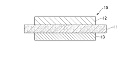
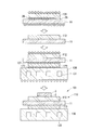
- the ceramic substrate 11 ceramic member
- the circuit layer 12 copper member
- the metal layer 13 copper member
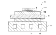
- FIG. 1 the power module 1 provided with the board
- the power module 1 includes a power module substrate 10 on which a circuit layer 12 is disposed, a semiconductor element 3 bonded to one surface (upper surface in FIG. 1) of the circuit layer 12 via a bonding layer 2, power And a heat sink 30 disposed on the other side (lower side in FIG. 1) of the module substrate 10.
- the power module substrate 10 includes a ceramic substrate 11, a circuit layer 12 disposed on one surface (the upper surface in FIG. 2) of the ceramic substrate 11, and the other surface of the ceramic substrate 11. And a metal layer 13 disposed on the lower surface in FIG.
- the ceramic substrate 11 is made of ceramics such as AlN (aluminum nitride), Si 3 N 4 (silicon nitride), and Al 2 O 3 (alumina) having high insulating properties. In this embodiment, it is comprised with AlN (aluminum nitride) excellent in heat dissipation. Further, the thickness of the ceramic substrate 11 is set within a range of 0.2 to 1.5 mm, and in this embodiment is set to 0.635 mm.
- the circuit layer 12 is formed by bonding a conductive copper or copper alloy metal plate to one surface of the ceramic substrate 11.
- the circuit layer 12 is formed by joining copper rolled sheets having a purity of 99.99% by mass or more. Note that the thickness of the circuit layer 12 is set in a range of 0.1 mm or more and 1.0 mm or less, and is set to 0.6 mm in the present embodiment.
- the metal layer 13 is formed by bonding a copper or copper alloy metal plate to the other surface of the ceramic substrate 11.
- the metal layer 13 is formed by joining copper rolled sheets having a purity of 99.99% by mass or more.
- the thickness of the metal layer 13 is set in the range of 0.1 mm or more and 1.0 mm or less, and is set to 0.6 mm in this embodiment.
- the semiconductor element 3 is made of a semiconductor material such as Si.
- the semiconductor element 3 and the circuit layer 12 are bonded via the bonding layer 2.
- the bonding layer 2 is made of, for example, a Sn—Ag, Sn—In, or Sn—Ag—Cu solder material.
- the heat sink 30 is for dissipating heat from the power module substrate 10 described above.
- the heat sink 30 is made of copper or a copper alloy, and in this embodiment is made of oxygen-free copper.
- the heat sink 30 is provided with a flow path 31 through which a cooling fluid flows.
- the heat sink 30 and the metal layer 13 are joined by a solder layer 18 made of a solder material.
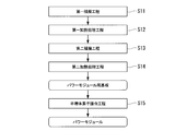
- the filler material 25, the active metal material 26, and the copper plate 22 to be the circuit layer 12 are sequentially laminated on one surface (the upper surface in FIG. 4) of the ceramic substrate 11.
- the filler material 25, the active metal material 26, and the copper plate 23 to be the metal layer 13 are sequentially laminated on the other surface 11 (the lower surface in FIG. 4).
- (Lamination process S01) That is, between the ceramic substrate 11 and the copper plate 22, the filler material 25 is disposed on the ceramic substrate 11 side, and the active metal material 26 is disposed on the copper plate 22 side.
- a filler material 25 is disposed on the substrate 11 side, and an active metal material 26 is disposed on the copper plate 22 side.
- the filler material 25 indicates a brazing material or a solder material, and has a melting point of 710 ° C. or lower, a Cu—P based brazing material, a Cu—Sn based brazing material, and a Cu—P—Sn—Ni based solder material.
- a Cu—Sn solder material is used.
- the Cu—P brazing material for example, a Cu—P brazing material, a Cu—P—Sn brazing material, a Cu—P—Sn—Ni brazing material, or the like can be used.
- a Cu—P—Sn—Ni-based brazing foil (Cu-7 mass% P-15 mass% Sn-10 mass% Ni) is used as the filler material 25.
- the thickness of the filler material 25 is in the range of 5 ⁇ m to 150 ⁇ m.
- the active metal material 26 contains, for example, one or more of active elements such as Ti, Zr, Nb, and Hf. In the present embodiment, a Ti foil is used as the active metal material 26. Yes.
- the thickness of the active metal material 26 is in the range of 1 ⁇ m to 20 ⁇ m.
- the ceramic substrate 11, the filler material 25, the active metal material 26, and the copper plates 22 and 23 are placed in a vacuum heating furnace in a state where the pressure is 1 to 35 kgf / cm 2 (98 to 3430 kPa) in the stacking direction. And heated (heat treatment step S02).
- the pressure in the vacuum heating furnace is in the range of 10 ⁇ 6 Pa to 10 ⁇ 3 Pa
- the heating temperature is in the range of 560 ° C. to 650 ° C.
- the heating time is 30 minutes or more. The range is set to 360 minutes or less.
- the active metal material 26 (Ti foil) and the copper plates 22 and 23 are joined by solid phase diffusion bonding, and the filler material 25 melts to form a liquid phase.
- the ceramic substrate 11 and the active metal material 26 are joined via the filler material 25.
- the joining surface of the active metal material 26 and the copper plates 22 and 23 to be joined by solid phase diffusion joining is a smooth surface in advance.
- the circuit layer 12 (copper member) and the metal layer 13 (copper member) are formed on one surface and the other surface of the ceramic substrate 11 (ceramic member), and the power module substrate 10 (bonding) according to the present embodiment. Body) is manufactured.
- the heat sink 30 is bonded to the lower surface of the metal layer 13 of the power module substrate 10 via a solder material (heat sink bonding step S03).
- the semiconductor element 3 is bonded to the upper surface of the circuit layer 12 of the power module substrate 10 via a solder material (semiconductor element bonding step S04). In this way, the power module 1 according to this embodiment is manufactured.
- the filler material 25 having a melting point of 710 ° C. or less is disposed between the ceramic substrate 11 and the copper plates 22 and 23 on the ceramic substrate 11 side. Since the heat treatment is performed with the active metal material 26 (Ti material in the present embodiment) disposed on the 23 side, Ti melts into the molten liquid phase melt material 25 during heating, and the liquid phase melt material. Thus, after the filler material 25 is solidified, the copper plate 22 is joined to the ceramic substrate 11 via the filler material 25, so that the joining reliability is high.
- the active metal material 26 and the copper plates 22 and 23 are laminated and heated and held at a temperature of 560 ° C. or higher and 650 ° C. or lower, so that Ti contained in the active metal material 26 is retained.
- the atoms can be diffused into the copper plates 22 and 23, the copper atoms contained in the copper plates 22 and 23 can be diffused into the active metal material 26, and the active metal material 26 and the copper plates 22 and 23 can be solid phase diffusion bonded.
- the heating temperature is 560 ° C. or higher, diffusion between Ti atoms contained in the active metal material 26 and copper atoms contained in the copper plates 22 and 23 is promoted, and solid phase diffusion can be sufficiently achieved in a short time. Moreover, when heating temperature is 650 degrees C or less, it can suppress that a liquid phase arises between the active metal material 26 and the copper plates 22 and 23, a bump arises in a joining interface, or thickness changes. Therefore, the heating temperature is set in the above range.
- the pressurized pressure is set in the above range.
- the melting point of the filler material 25 is 710 ° C. or less, the liquid phase of the filler material can be formed at a lower temperature than when the Ag—Cu—Ti brazing material is used. Furthermore, since the active metal material 26 is interposed between the filler material 25 and the copper plates 22 and 23, the liquid phase of the filler material 25 and the copper plates 22 and 23 are not in direct contact with each other at the bonding interface. It is possible to suppress the occurrence of bumps and fluctuations in thickness.
- the filler material 25 is well bonded to the ceramic substrate 11 and the active metal material 26 and the copper plates 22 and 23 are bonded by solid phase diffusion bonding, the ceramic substrate 11 and the copper plates 22 and 23 are bonded. And the bonding reliability between the ceramic substrate 11 and the circuit layer 12 and the metal layer 13 can be improved. Further, since the ceramic substrate 11 and the copper plates 22 and 23 are joined using the filler material 25 not containing Ag, the manufacturing cost can be reduced as compared with the case where the Ag—Cu—Ti brazing material is used.
- the manufacturing process can be simplified and the manufacturing cost can be reduced. Furthermore, since the surface where the active metal material 26 and the copper plates 22 and 23 are joined is a smooth surface in advance, it is possible to suppress the formation of a gap at the joining interface, and the active metal material 26 and the copper plates 22 and 23 Can be reliably joined.
- the circuit layer 12 made of the copper plate 22 is formed on one surface of the ceramic substrate 11, so that the heat from the semiconductor element 3 is spread. Can be diffused to the ceramic substrate 11 side. Moreover, since the deformation resistance of the copper plate 22 is large, the deformation of the circuit layer 12 is suppressed when a heat cycle is applied, and the deformation of the bonding layer 2 that bonds the semiconductor element 3 and the circuit layer 12 is suppressed. Reliability can be improved. Further, since the metal layer 13 made of the copper plate 23 is formed on the other surface of the ceramic substrate 11, the heat from the semiconductor element 3 can be efficiently transmitted to the heat sink 30 side.
- the power module 101 includes a power module substrate 110 on which a circuit layer 112 is disposed, a semiconductor element 3 bonded to one surface (the upper surface in FIG. 5) of the circuit layer 112 via a bonding layer 2, a power And a heat sink 130 disposed on the other side (lower side in FIG. 5) of the module substrate 110.
- the power module substrate 110 includes a ceramic substrate 11, a circuit layer 112 disposed on one surface (the upper surface in FIG. 5) of the ceramic substrate 11, and the other surface of the ceramic substrate 11. And a metal layer 113 disposed on the lower surface in FIG.
- the circuit layer 112 is formed by joining a conductive copper or copper alloy metal plate to one surface of the ceramic substrate 11.
- the circuit layer 112 is formed by joining copper rolled sheets having a purity of 99.99% by mass or more. Note that the thickness of the circuit layer 112 is set in a range of 0.1 mm or more and 1.0 mm or less, and is set to 0.4 mm in the present embodiment.
- the metal layer 113 is formed by joining an aluminum or aluminum alloy metal plate to the other surface of the ceramic substrate 11.
- the metal layer 113 is formed by joining aluminum rolled sheets having a purity of 99.99% by mass or more. Note that the thickness of the metal layer 113 is set within a range of 0.1 mm to 3.0 mm, and is set to 2.1 mm in the present embodiment.
- the heat sink 130 is for dissipating heat from the power module substrate 110 described above.
- the heat sink 130 is made of aluminum or an aluminum alloy.
- the heat sink 130 is made of A6063 (aluminum alloy).
- the heat sink 130 is provided with a flow path 131 through which a cooling fluid flows.
- the heat sink 130 and the metal layer 113 are joined by an Al—Si brazing material.
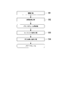
- the filler material 25, the active metal material 26, and the copper plate 122 to be the circuit layer 112 are sequentially laminated on one surface (the upper surface in FIG. 7) of the ceramic substrate 11 (first laminated layer).
- Step S11 That is, between the ceramic substrate 11 and the copper plate 122, the filler material 25 is disposed on the ceramic substrate 11 side, and the active metal material 26 is disposed on the copper plate 122 side.
- a Cu—P—Sn—Ni brazing filler metal foil (Cu-7 mass% P-15 mass% Sn-10 mass% Ni) is used as the filler material 25.
- the thickness of the filler material 25 is in the range of 5 ⁇ m to 150 ⁇ m.
- Ti foil is used as the active metal material 26.
- the thickness of the active metal material 26 is in the range of 1 ⁇ m to 20 ⁇ m.
- the ceramic substrate 11, the filler material 25, the active metal material 26, and the copper plate 122 were charged in a vacuum heating furnace in a state where the pressure was 1 to 35 kgf / cm 2 (98 to 3430 kPa) in the stacking direction. And heated (first heat treatment step S12).
- the pressure in the vacuum heating furnace is in the range of 10 ⁇ 6 Pa to 10 ⁇ 3 Pa
- the heating temperature is in the range of 560 ° C. to 650 ° C.
- the heating time is 30 minutes or more.
- the range is set to 360 minutes or less.
- the copper plate 122 is bonded to one surface of the ceramic substrate 11 to form the circuit layer 112.
- an aluminum plate 123 to be the metal layer 113 is laminated on the other surface (the lower surface in FIG. 7) of the ceramic substrate 11 via the Al—Si brazing material 127 (second lamination step). S13).
- a heat sink 130 was further laminated below the aluminum plate 123 via an Al—Si brazing material 127.
- the ceramic substrate 11, the aluminum plate 123, and the heat sink 130 are charged in a vacuum heating furnace and heated in a state in which the pressure is 1 to 35 kgf / cm 2 (98 to 3430 kPa) in the stacking direction (second).
- Heat treatment step S14 the pressure in the vacuum heating furnace is in the range of 10 ⁇ 6 Pa to 10 ⁇ 3 Pa
- the heating temperature is in the range of 600 ° C. to 650 ° C.
- the heating time is 30 minutes or more.
- the range is set to 180 minutes or less.
- the aluminum plate 123 is joined to the other surface of the ceramic substrate 11 to form the metal layer 113, and the power module substrate 110 of the second embodiment is manufactured.
- the heat sink 130 is bonded to the substrate.
- the semiconductor element 3 is bonded to the upper surface of the circuit layer 112 of the power module substrate 110 via a solder material (semiconductor element bonding step S15). In this way, the power module 101 of the second embodiment is manufactured.
- the filler material 25 having a melting point of 710 ° C. or less is disposed on the ceramic substrate 11 side between the ceramic substrate 11 and the copper plate 122, and on the copper plate 122 side. Since the heat treatment is performed in a state where the active metal material 26 (Ti material) is arranged, Ti is dissolved in the liquid phase in which the filler material 25 is melted during heating, and the wettability between the liquid phase of the filler material 25 and the ceramic substrate 11. becomes better. Therefore, when the liquid phase of the filler material 25 is solidified, the bonding reliability between the filler material 25 and the ceramic substrate 11 is improved.
- the active metal material 26 and the copper plate 122 are laminated and pressed and heated to a temperature of 560 ° C. or more and 650 ° C. or less, so that the active metal material 26 and the copper plate 122 are fixed. Phase diffusion bonding can be performed.
- the metal layer 113 made of the aluminum plate 123 is formed on the other surface of the ceramic substrate 11, so that the power module substrate is loaded when a cooling cycle is applied.
- the thermal stress generated between 110 and the heat sink 130 can be absorbed by the metal layer 113, and the occurrence of cracks in the ceramic substrate 11 can be suppressed.
- the metal layer is formed on the other surface of the ceramic substrate.
- the metal layer may not be formed.
- the filler material is a Cu—P—Sn—Ni-based brazing material having a melting point of 710 ° C. or less has been described.
- the filler material has a melting point (solidus temperature).
- the brazing material may be 710 ° C. or lower and the liquidus temperature 450 ° C. or higher.
- this brazing material may be any one selected from Cu—P based brazing material, Cu—Sn based brazing material, and Cu—Al based brazing material.
- the Cu—P brazing material for example, a Cu—P brazing material, a Cu—P—Sn brazing material, or the like can be used.
- the filler material may be a solder material having a liquidus temperature of less than 450 ° C.
- the solder material may be a Cu—P—Sn—Ni solder material or a Cu—Sn solder material.
- an active metal material 226 is disposed on the ceramic member 211 by sputtering or the like, a filler material 225 is disposed between the active metal material 226 and the copper member 222, and these are laminated. It is possible to join the active metal material 226 and the copper member 222 by performing heat treatment by applying pressure in the stacking direction.
- inventive examples 1 to 10 on one side and the other side of a ceramic substrate made of AlN (40 mm ⁇ 40 mm ⁇ 0.635 mmt (thickness)), the filler material, active metal material, purity 99 shown in Table 1 were used.
- a copper plate (37 mm ⁇ 37 mm ⁇ 0.3 mmt) made of 99% copper is laminated.
- a copper plate (37 mm ⁇ 37 mm ⁇ 40 mm ⁇ 0.635 mmt) made of AlN, a filler material, an active metal material, and a purity 99.99% copper shown in Table 1 on one surface of the ceramic substrate (40 mm ⁇ 40 mm ⁇ 0.635 mmt). 37 mm ⁇ 0.3 mmt).
- the ceramic substrate / the filler material / the active metal material / the copper plate are laminated in this order.
- Example 10 of the present invention in which the position of the substrate was the ceramic substrate side, the layers were laminated in the order of ceramic substrate / active metal material / filler material / copper plate.
- the ceramic substrate was loaded into the vacuum heating furnace in a state pressurized at a pressure of 15 kgf / cm 2 (1470 kPa) in the laminating direction and heated to heat the one surface of the ceramic substrate and the other surface.
- a copper plate was joined to the surface to form a circuit layer and a metal layer.
- the pressure in the vacuum heating furnace was set within the range of 10 ⁇ 6 Pa or more and 10 ⁇ 3 Pa or less, and the heating temperature and the heating time were set as shown in Table 1. In this way, power module substrates of Invention Examples 1 to 9 were obtained.
- Example 11 of the present invention a copper plate was joined to one surface of the ceramic substrate by charging in a vacuum heating furnace in a state pressurized at a pressure of 15 kgf / cm 2 (1470 kPa) in the laminating direction, Formed.
- the pressure in the vacuum heating furnace was set within the range of 10 ⁇ 6 Pa or more and 10 ⁇ 3 Pa or less, and the heating temperature and the heating time were set as shown in Table 1.
- an aluminum plate made of aluminum having a purity of 99.99% by mass is laminated on the other surface of the ceramic substrate via an Al—Si brazing filler metal and pressed in the laminating direction at 5 kgf / cm 2 (490 kPa).
- the heat sink was a copper plate (50 mm ⁇ 60 mm ⁇ 5 mmt) made of phosphorous deoxidized copper.
- the bonding conditions were Sn-Sb solder material and heating at 270 ° C. In this way, power module substrates with heat sinks of Invention Examples 1 to 11 were produced.
- the bonding rate between the circuit layer and the ceramic substrate and the bonding rate between the circuit layer and the ceramic substrate after the thermal cycle test were evaluated. .
- a test method for the cooling / heating cycle and a method for evaluating the bonding rate will be described below.
- the thermal cycle test uses TSB-51 made by ESP Co., Ltd., and the power module substrate with a heat sink is maintained in a liquid phase (Fluorinert) for 5 minutes in a temperature environment of ⁇ 40 ° C., and then 125 ° C. The temperature change process was continued for 5 minutes and maintained in the same temperature environment for 5 minutes, and the process of returning to the temperature environment at ⁇ 40 ° C. was taken as one cycle.
- TSB-51 made by ESP Co., Ltd.
- the bonding rate at the interface between the ceramic substrate and the circuit layer was evaluated using an ultrasonic flaw detector and calculated from the following equation.
- the initial bonding area is the area to be bonded before bonding, that is, the area of the circuit layer in this embodiment.
- peeling is indicated by a white portion in the joint, and thus the area of the white portion was taken as the peeling area.
- this crack is shown by a white part in an ultrasonic flaw detection image, and a crack will also be evaluated as a peeling area.
- Table 1 The results of the above evaluation are shown in Table 1.
- the present invention relates to a method for manufacturing a power module substrate, which can join a ceramic member and a copper member at a low temperature and has a low manufacturing cost.
Landscapes
- Engineering & Computer Science (AREA)
- Chemical & Material Sciences (AREA)
- Ceramic Engineering (AREA)
- Materials Engineering (AREA)
- General Physics & Mathematics (AREA)
- Condensed Matter Physics & Semiconductors (AREA)
- Physics & Mathematics (AREA)
- Computer Hardware Design (AREA)
- Microelectronics & Electronic Packaging (AREA)
- Power Engineering (AREA)
- Structural Engineering (AREA)
- Organic Chemistry (AREA)
- Manufacturing & Machinery (AREA)
- Cooling Or The Like Of Semiconductors Or Solid State Devices (AREA)
- Ceramic Products (AREA)
Priority Applications (4)
| Application Number | Priority Date | Filing Date | Title |
|---|---|---|---|
| US14/775,819 US10199237B2 (en) | 2013-03-18 | 2014-03-17 | Method for manufacturing bonded body and method for manufacturing power-module substrate |
| EP14769861.7A EP2978019B1 (en) | 2013-03-18 | 2014-03-17 | Method for manufacturing bonded body and method for manufacturing power-module substrate |
| CN201480012947.2A CN105190869B (zh) | 2013-03-18 | 2014-03-17 | 接合体的制造方法、及功率模块用基板的制造方法 |
| KR1020157025321A KR102220852B1 (ko) | 2013-03-18 | 2014-03-17 | 접합체의 제조 방법 및 파워 모듈용 기판의 제조 방법 |
Applications Claiming Priority (2)
| Application Number | Priority Date | Filing Date | Title |
|---|---|---|---|
| JP2013-055517 | 2013-03-18 | ||
| JP2013055517A JP5672324B2 (ja) | 2013-03-18 | 2013-03-18 | 接合体の製造方法及びパワーモジュール用基板の製造方法 |
Publications (1)
| Publication Number | Publication Date |
|---|---|
| WO2014148425A1 true WO2014148425A1 (ja) | 2014-09-25 |
Family
ID=51580104
Family Applications (1)
| Application Number | Title | Priority Date | Filing Date |
|---|---|---|---|
| PCT/JP2014/057121 WO2014148425A1 (ja) | 2013-03-18 | 2014-03-17 | 接合体の製造方法及びパワーモジュール用基板の製造方法 |
Country Status (7)
Families Citing this family (20)
| Publication number | Priority date | Publication date | Assignee | Title |
|---|---|---|---|---|
| JP6111764B2 (ja) * | 2013-03-18 | 2017-04-12 | 三菱マテリアル株式会社 | パワーモジュール用基板の製造方法 |
| JP5672324B2 (ja) | 2013-03-18 | 2015-02-18 | 三菱マテリアル株式会社 | 接合体の製造方法及びパワーモジュール用基板の製造方法 |
| WO2015029811A1 (ja) * | 2013-08-26 | 2015-03-05 | 三菱マテリアル株式会社 | 接合体及びパワーモジュール用基板 |
| JP6079505B2 (ja) | 2013-08-26 | 2017-02-15 | 三菱マテリアル株式会社 | 接合体及びパワーモジュール用基板 |
| JP5720839B2 (ja) | 2013-08-26 | 2015-05-20 | 三菱マテリアル株式会社 | 接合体及びパワーモジュール用基板 |
| JP6127833B2 (ja) | 2013-08-26 | 2017-05-17 | 三菱マテリアル株式会社 | 接合体の製造方法及びパワーモジュール用基板の製造方法 |
| JP6256176B2 (ja) * | 2014-04-25 | 2018-01-10 | 三菱マテリアル株式会社 | 接合体の製造方法、パワーモジュール用基板の製造方法 |
| JP6819299B2 (ja) | 2016-01-22 | 2021-01-27 | 三菱マテリアル株式会社 | 接合体、パワーモジュール用基板、接合体の製造方法及びパワーモジュール用基板の製造方法 |
| CN109075135B (zh) * | 2016-01-22 | 2022-04-05 | 三菱综合材料株式会社 | 接合体、功率模块用基板、接合体的制造方法及功率模块用基板的制造方法 |
| JP6652856B2 (ja) * | 2016-02-25 | 2020-02-26 | 株式会社フジクラ | 半導体レーザモジュール及びその製造方法 |
| JP7124633B2 (ja) * | 2017-10-27 | 2022-08-24 | 三菱マテリアル株式会社 | 接合体、及び、絶縁回路基板 |
| KR102483328B1 (ko) | 2017-11-13 | 2022-12-30 | 삼성전자주식회사 | 복수개의 전자 장치들 간의 거리 측정 방법 및 그에 따른 전자 장치 |
| US11476127B2 (en) * | 2018-03-23 | 2022-10-18 | Mitsubishi Materials Corporation | Manufacturing method of electronic-component-mounted module |
| EP3780087B1 (en) * | 2018-03-26 | 2025-07-30 | Mitsubishi Materials Corporation | Method of manufacturing bonded body for insulating circuit board, and bonded body for insulating circuit board |
| WO2020044594A1 (ja) | 2018-08-28 | 2020-03-05 | 三菱マテリアル株式会社 | 銅/セラミックス接合体、絶縁回路基板、及び、銅/セラミックス接合体の製造方法、及び、絶縁回路基板の製造方法 |
| DE102019135171A1 (de) * | 2019-12-19 | 2021-06-24 | Rogers Germany Gmbh | Lotmaterial, Verfahren zur Herstellung eines solchen Lotmaterials und Verwendung eines solchen Lotmaterials zur Anbindung einer Metallschicht an eine Keramikschicht |
| CN112289763A (zh) * | 2020-06-12 | 2021-01-29 | 无锡利普思半导体有限公司 | 一种功率半导体模块 |
| WO2022075409A1 (ja) * | 2020-10-07 | 2022-04-14 | 株式会社 東芝 | 接合体、セラミックス回路基板、および半導体装置 |
| CN112811922B (zh) * | 2021-01-20 | 2021-11-02 | 中国科学院上海硅酸盐研究所 | 一种覆铜板的氮化硅陶瓷基片及其制备方法 |
| TWI851321B (zh) * | 2023-07-06 | 2024-08-01 | 同欣電子工業股份有限公司 | 活性金屬硬焊基板材料及其製造方法 |
Citations (5)
| Publication number | Priority date | Publication date | Assignee | Title |
|---|---|---|---|---|
| JP3211856B2 (ja) | 1994-11-02 | 2001-09-25 | 電気化学工業株式会社 | 回路基板 |
| JP2003197826A (ja) * | 2001-12-26 | 2003-07-11 | Toshiba Corp | セラミックス回路基板およびそれを用いた半導体モジュール |
| JP2005035874A (ja) * | 2003-03-27 | 2005-02-10 | Dowa Mining Co Ltd | 金属−セラミックス接合基板の製造方法 |
| JP2005050919A (ja) * | 2003-07-30 | 2005-02-24 | Ngk Spark Plug Co Ltd | 回路基板および半導体装置 |
| JP2011155227A (ja) * | 2010-01-28 | 2011-08-11 | Honda Motor Co Ltd | 半導体装置及びその製造方法 |
Family Cites Families (51)
| Publication number | Priority date | Publication date | Assignee | Title |
|---|---|---|---|---|
| US153618A (en) * | 1874-07-28 | Improvement in lock-hinges | ||
| JPH0810710B2 (ja) * | 1984-02-24 | 1996-01-31 | 株式会社東芝 | 良熱伝導性基板の製造方法 |
| JPS63239166A (ja) | 1987-03-27 | 1988-10-05 | 株式会社東芝 | セラミツクス接合体 |
| US5378294A (en) | 1989-11-17 | 1995-01-03 | Outokumpu Oy | Copper alloys to be used as brazing filler metals |
| JPH03297595A (ja) * | 1990-04-18 | 1991-12-27 | Meidensha Corp | ロウ材とロウ付け方法 |
| US5561321A (en) | 1992-07-03 | 1996-10-01 | Noritake Co., Ltd. | Ceramic-metal composite structure and process of producing same |
| JPH07308794A (ja) * | 1994-05-19 | 1995-11-28 | Showa Alum Corp | 低温ろう付用ろう材 |
| JP4077888B2 (ja) * | 1995-07-21 | 2008-04-23 | 株式会社東芝 | セラミックス回路基板 |
| JPH10102167A (ja) * | 1996-09-25 | 1998-04-21 | Toyota Central Res & Dev Lab Inc | 銅系低融点ろう材 |
| KR100371974B1 (ko) * | 1997-05-26 | 2003-02-17 | 스미토모덴키고교가부시키가이샤 | 구리회로접합기판 및 그 제조방법 |
| JP2000119071A (ja) | 1998-10-14 | 2000-04-25 | Fuji Electric Co Ltd | 半導体装置用セラミックス基板 |
| JP2001148451A (ja) | 1999-03-24 | 2001-05-29 | Mitsubishi Materials Corp | パワーモジュール用基板 |
| JP2000349400A (ja) | 1999-06-04 | 2000-12-15 | Denki Kagaku Kogyo Kk | 回路基板 |
| US20030091463A1 (en) | 2001-02-27 | 2003-05-15 | Koichi Izumida | Unleaded solder alloy and electronic components using it |
| US9533379B2 (en) * | 2002-08-23 | 2017-01-03 | Lincoln Global, Inc. | Phosphorous-copper base brazing alloy |
| JP4206915B2 (ja) | 2002-12-27 | 2009-01-14 | 三菱マテリアル株式会社 | パワーモジュール用基板 |
| CA2525386A1 (en) | 2003-05-13 | 2005-01-20 | Reactive Nanotechnologies, Inc. | Method of controlling thermal waves in reactive multilayer joining and resulting product |
| JP4362597B2 (ja) | 2003-05-30 | 2009-11-11 | Dowaメタルテック株式会社 | 金属−セラミックス回路基板およびその製造方法 |
| JP2005052869A (ja) | 2003-08-06 | 2005-03-03 | Sumitomo Metal Mining Co Ltd | 高温はんだ付用ろう材とそれを用いた半導体装置 |
| JP4115979B2 (ja) | 2004-09-24 | 2008-07-09 | 株式会社東芝 | 非鉛系はんだ材 |
| JP4207896B2 (ja) | 2005-01-19 | 2009-01-14 | 富士電機デバイステクノロジー株式会社 | 半導体装置 |
| EP1858078A4 (en) | 2005-01-20 | 2009-03-04 | Almt Corp | ELEMENT FOR A SEMICONDUCTOR COMPONENT AND MANUFACTURING METHOD THEREFOR |
| DE102005032076B3 (de) | 2005-07-08 | 2007-02-08 | Infineon Technologies Ag | Verfahren zum Herstellen eines Schaltungsmoduls |
| DE102005061049A1 (de) | 2005-12-19 | 2007-06-21 | Curamik Electronics Gmbh | Metall-Keramik-Substrat |
| US8164176B2 (en) | 2006-10-20 | 2012-04-24 | Infineon Technologies Ag | Semiconductor module arrangement |
| JP2008198706A (ja) | 2007-02-09 | 2008-08-28 | Hitachi Metals Ltd | 回路基板、その製造方法およびそれを用いた半導体モジュール |
| JP4964009B2 (ja) | 2007-04-17 | 2012-06-27 | 株式会社豊田中央研究所 | パワー半導体モジュール |
| CN101687717A (zh) | 2007-04-24 | 2010-03-31 | 陶瓷技术股份公司 | 具有一种金属化陶瓷体的构件 |
| US7821130B2 (en) | 2008-03-31 | 2010-10-26 | Infineon Technologies Ag | Module including a rough solder joint |
| CN102047413B (zh) | 2008-06-06 | 2015-04-15 | 三菱综合材料株式会社 | 功率模块用基板、功率模块以及功率模块用基板的制造方法 |
| US20100175756A1 (en) | 2009-01-15 | 2010-07-15 | Weihs Timothy P | Method For Bonding Of Concentrating Photovoltaic Receiver Module To Heat Sink Using Foil And Solder |
| GB2479844B (en) | 2009-01-29 | 2013-06-19 | Smith International | Brazing methods for PDC cutters |
| JP5504842B2 (ja) | 2009-11-20 | 2014-05-28 | 三菱マテリアル株式会社 | パワーモジュール用基板、ヒートシンク付パワーモジュール用基板、パワーモジュール及びパワーモジュール用基板の製造方法 |
| JP5577980B2 (ja) | 2010-09-16 | 2014-08-27 | 三菱マテリアル株式会社 | ヒートシンク付パワーモジュール用基板、パワーモジュール及びヒートシンク付パワーモジュール用基板の製造方法 |
| JP2012136378A (ja) | 2010-12-25 | 2012-07-19 | Kyocera Corp | 回路基板およびこれを用いた電子装置 |
| JP5736807B2 (ja) | 2011-02-02 | 2015-06-17 | 三菱マテリアル株式会社 | ヒートシンク付パワーモジュール用基板、ヒートシンク付パワーモジュール用基板の製造方法及びパワーモジュール |
| JP2012178513A (ja) | 2011-02-28 | 2012-09-13 | Mitsubishi Materials Corp | パワーモジュールユニット及びパワーモジュールユニットの製造方法 |
| EP2734484A1 (en) | 2011-07-20 | 2014-05-28 | Diamond Innovations, Inc. | Brazed coated diamond-containing materials |
| CN103703560B (zh) | 2011-08-04 | 2016-07-20 | 三菱电机株式会社 | 半导体装置及其制造方法 |
| JP5218621B2 (ja) * | 2011-10-28 | 2013-06-26 | 日立金属株式会社 | 回路基板およびこれを用いた半導体モジュール |
| CN104067386B (zh) | 2012-02-01 | 2019-05-28 | 三菱综合材料株式会社 | 功率模块用基板的制造方法 |
| JP2013229579A (ja) | 2012-03-30 | 2013-11-07 | Mitsubishi Materials Corp | パワーモジュール用基板、ヒートシンク付パワーモジュール用基板及びパワーモジュール |
| JP6044097B2 (ja) | 2012-03-30 | 2016-12-14 | 三菱マテリアル株式会社 | ヒートシンク付パワーモジュール用基板、冷却器付パワーモジュール用基板及びパワーモジュール |
| CN104718616B (zh) | 2012-10-16 | 2017-11-14 | 三菱综合材料株式会社 | 自带散热器的功率模块用基板、自带散热器的功率模块及自带散热器的功率模块用基板的制造方法 |
| CN102922828B (zh) | 2012-10-24 | 2015-04-22 | 浙江工贸职业技术学院 | 铜箔键合陶瓷基板的复合板及其制备方法 |
| JP6056432B2 (ja) | 2012-12-06 | 2017-01-11 | 三菱マテリアル株式会社 | パワーモジュール用基板、ヒートシンク付パワーモジュール用基板、パワーモジュール、パワーモジュール用基板の製造方法 |
| JP5664679B2 (ja) | 2013-03-07 | 2015-02-04 | 三菱マテリアル株式会社 | パワーモジュール用基板の製造方法 |
| TWI604574B (zh) | 2013-03-14 | 2017-11-01 | 三菱綜合材料股份有限公司 | 接合體、電源模組用基板及附散熱片之電源模組用基板 |
| JP6111764B2 (ja) * | 2013-03-18 | 2017-04-12 | 三菱マテリアル株式会社 | パワーモジュール用基板の製造方法 |
| JP5672324B2 (ja) | 2013-03-18 | 2015-02-18 | 三菱マテリアル株式会社 | 接合体の製造方法及びパワーモジュール用基板の製造方法 |
| JP3211856U (ja) | 2017-05-09 | 2017-08-10 | 株式会社アイエスピー | メジャー付きタオル |
-
2013
- 2013-03-18 JP JP2013055517A patent/JP5672324B2/ja active Active
-
2014
- 2014-03-17 WO PCT/JP2014/057121 patent/WO2014148425A1/ja active Application Filing
- 2014-03-17 EP EP14769861.7A patent/EP2978019B1/en active Active
- 2014-03-17 CN CN201480012947.2A patent/CN105190869B/zh active Active
- 2014-03-17 US US14/775,819 patent/US10199237B2/en active Active
- 2014-03-17 KR KR1020157025321A patent/KR102220852B1/ko active Active
- 2014-03-18 TW TW103110092A patent/TWI609461B/zh active
Patent Citations (5)
| Publication number | Priority date | Publication date | Assignee | Title |
|---|---|---|---|---|
| JP3211856B2 (ja) | 1994-11-02 | 2001-09-25 | 電気化学工業株式会社 | 回路基板 |
| JP2003197826A (ja) * | 2001-12-26 | 2003-07-11 | Toshiba Corp | セラミックス回路基板およびそれを用いた半導体モジュール |
| JP2005035874A (ja) * | 2003-03-27 | 2005-02-10 | Dowa Mining Co Ltd | 金属−セラミックス接合基板の製造方法 |
| JP2005050919A (ja) * | 2003-07-30 | 2005-02-24 | Ngk Spark Plug Co Ltd | 回路基板および半導体装置 |
| JP2011155227A (ja) * | 2010-01-28 | 2011-08-11 | Honda Motor Co Ltd | 半導体装置及びその製造方法 |
Non-Patent Citations (1)
| Title |
|---|
| See also references of EP2978019A4 |
Also Published As
| Publication number | Publication date |
|---|---|
| TWI609461B (zh) | 2017-12-21 |
| JP2014183118A (ja) | 2014-09-29 |
| TW201508870A (zh) | 2015-03-01 |
| KR102220852B1 (ko) | 2021-02-25 |
| CN105190869B (zh) | 2018-08-10 |
| US10199237B2 (en) | 2019-02-05 |
| KR20150133194A (ko) | 2015-11-27 |
| CN105190869A (zh) | 2015-12-23 |
| EP2978019B1 (en) | 2018-01-31 |
| EP2978019A1 (en) | 2016-01-27 |
| EP2978019A4 (en) | 2016-11-02 |
| JP5672324B2 (ja) | 2015-02-18 |
| US20160013073A1 (en) | 2016-01-14 |
Similar Documents
| Publication | Publication Date | Title |
|---|---|---|
| WO2014148425A1 (ja) | 接合体の製造方法及びパワーモジュール用基板の製造方法 | |
| JP6111764B2 (ja) | パワーモジュール用基板の製造方法 | |
| JP6079505B2 (ja) | 接合体及びパワーモジュール用基板 | |
| JP5403129B2 (ja) | パワーモジュール用基板、ヒートシンク付パワーモジュール用基板、パワーモジュール、及びパワーモジュール用基板の製造方法 | |
| KR102154889B1 (ko) | 접합체의 제조 방법 및 파워 모듈용 기판의 제조 방법 | |
| KR20190123727A (ko) | 구리/세라믹스 접합체, 절연 회로 기판, 및, 구리/세라믹스 접합체의 제조 방법, 절연 회로 기판의 제조 방법 | |
| JP5720839B2 (ja) | 接合体及びパワーモジュール用基板 | |
| JP2016219852A (ja) | 冷却器付パワーモジュール用基板及びその製造方法 | |
| JP6256176B2 (ja) | 接合体の製造方法、パワーモジュール用基板の製造方法 | |
| JP5725061B2 (ja) | パワーモジュール用基板、及びヒートシンク付パワーモジュール用基板 | |
| JP6432208B2 (ja) | パワーモジュール用基板の製造方法、及び、ヒートシンク付パワーモジュール用基板の製造方法 | |
| JP5904257B2 (ja) | パワーモジュール用基板の製造方法 | |
| JP6303420B2 (ja) | パワーモジュール用基板 | |
| JP2014039062A (ja) | パワーモジュール用基板、ヒートシンク付パワーモジュール用基板、パワーモジュール、及びパワーモジュール用基板の製造方法 | |
| JP6327058B2 (ja) | ヒートシンク付パワーモジュール用基板、接合体の製造方法、パワーモジュール用基板の製造方法、及び、ヒートシンク付パワーモジュール用基板の製造方法 | |
| WO2016060079A1 (ja) | 冷却器付パワーモジュール用基板及びその製造方法 |
Legal Events
| Date | Code | Title | Description |
|---|---|---|---|
| WWE | Wipo information: entry into national phase |
Ref document number: 201480012947.2 Country of ref document: CN |
|
| 121 | Ep: the epo has been informed by wipo that ep was designated in this application |
Ref document number: 14769861 Country of ref document: EP Kind code of ref document: A1 |
|
| WWE | Wipo information: entry into national phase |
Ref document number: 2014769861 Country of ref document: EP |
|
| WWE | Wipo information: entry into national phase |
Ref document number: 14775819 Country of ref document: US |
|
| ENP | Entry into the national phase |
Ref document number: 20157025321 Country of ref document: KR Kind code of ref document: A |
|
| NENP | Non-entry into the national phase |
Ref country code: DE |