WO2014136591A1 - 薄膜トランジスタおよびその製造方法 - Google Patents
薄膜トランジスタおよびその製造方法 Download PDFInfo
- Publication number
- WO2014136591A1 WO2014136591A1 PCT/JP2014/054213 JP2014054213W WO2014136591A1 WO 2014136591 A1 WO2014136591 A1 WO 2014136591A1 JP 2014054213 W JP2014054213 W JP 2014054213W WO 2014136591 A1 WO2014136591 A1 WO 2014136591A1
- Authority
- WO
- WIPO (PCT)
- Prior art keywords
- thin film
- carbon nanowall
- channel layer
- silicon substrate
- film transistor
- Prior art date
- Legal status (The legal status is an assumption and is not a legal conclusion. Google has not performed a legal analysis and makes no representation as to the accuracy of the status listed.)
- Ceased
Links
Images













Classifications
-
- H—ELECTRICITY
- H10—SEMICONDUCTOR DEVICES; ELECTRIC SOLID-STATE DEVICES NOT OTHERWISE PROVIDED FOR
- H10D—INORGANIC ELECTRIC SEMICONDUCTOR DEVICES
- H10D62/00—Semiconductor bodies, or regions thereof, of devices having potential barriers
- H10D62/10—Shapes, relative sizes or dispositions of the regions of the semiconductor bodies; Shapes of the semiconductor bodies
- H10D62/117—Shapes of semiconductor bodies
- H10D62/118—Nanostructure semiconductor bodies
-
- H—ELECTRICITY
- H10—SEMICONDUCTOR DEVICES; ELECTRIC SOLID-STATE DEVICES NOT OTHERWISE PROVIDED FOR
- H10D—INORGANIC ELECTRIC SEMICONDUCTOR DEVICES
- H10D30/00—Field-effect transistors [FET]
- H10D30/01—Manufacture or treatment
- H10D30/021—Manufacture or treatment of FETs having insulated gates [IGFET]
- H10D30/031—Manufacture or treatment of FETs having insulated gates [IGFET] of thin-film transistors [TFT]
-
- H—ELECTRICITY
- H10—SEMICONDUCTOR DEVICES; ELECTRIC SOLID-STATE DEVICES NOT OTHERWISE PROVIDED FOR
- H10D—INORGANIC ELECTRIC SEMICONDUCTOR DEVICES
- H10D30/00—Field-effect transistors [FET]
- H10D30/40—FETs having zero-dimensional [0D], one-dimensional [1D] or two-dimensional [2D] charge carrier gas channels
- H10D30/47—FETs having zero-dimensional [0D], one-dimensional [1D] or two-dimensional [2D] charge carrier gas channels having two-dimensional [2D] charge carrier gas channels, e.g. nanoribbon FETs or high electron mobility transistors [HEMT]
-
- H—ELECTRICITY
- H10—SEMICONDUCTOR DEVICES; ELECTRIC SOLID-STATE DEVICES NOT OTHERWISE PROVIDED FOR
- H10D—INORGANIC ELECTRIC SEMICONDUCTOR DEVICES
- H10D30/00—Field-effect transistors [FET]
- H10D30/60—Insulated-gate field-effect transistors [IGFET]
- H10D30/67—Thin-film transistors [TFT]
- H10D30/674—Thin-film transistors [TFT] characterised by the active materials
- H10D30/6741—Group IV materials, e.g. germanium or silicon carbide
-
- H—ELECTRICITY
- H10—SEMICONDUCTOR DEVICES; ELECTRIC SOLID-STATE DEVICES NOT OTHERWISE PROVIDED FOR
- H10D—INORGANIC ELECTRIC SEMICONDUCTOR DEVICES
- H10D30/00—Field-effect transistors [FET]
- H10D30/60—Insulated-gate field-effect transistors [IGFET]
- H10D30/67—Thin-film transistors [TFT]
- H10D30/6758—Thin-film transistors [TFT] characterised by the insulating substrates
-
- H—ELECTRICITY
- H10—SEMICONDUCTOR DEVICES; ELECTRIC SOLID-STATE DEVICES NOT OTHERWISE PROVIDED FOR
- H10D—INORGANIC ELECTRIC SEMICONDUCTOR DEVICES
- H10D62/00—Semiconductor bodies, or regions thereof, of devices having potential barriers
- H10D62/80—Semiconductor bodies, or regions thereof, of devices having potential barriers characterised by the materials
- H10D62/881—Semiconductor bodies, or regions thereof, of devices having potential barriers characterised by the materials being a two-dimensional material
- H10D62/882—Graphene
-
- H—ELECTRICITY
- H10—SEMICONDUCTOR DEVICES; ELECTRIC SOLID-STATE DEVICES NOT OTHERWISE PROVIDED FOR
- H10K—ORGANIC ELECTRIC SOLID-STATE DEVICES
- H10K85/00—Organic materials used in the body or electrodes of devices covered by this subclass
- H10K85/20—Carbon compounds, e.g. carbon nanotubes or fullerenes
-
- H—ELECTRICITY
- H10—SEMICONDUCTOR DEVICES; ELECTRIC SOLID-STATE DEVICES NOT OTHERWISE PROVIDED FOR
- H10K—ORGANIC ELECTRIC SOLID-STATE DEVICES
- H10K10/00—Organic devices specially adapted for rectifying, amplifying, oscillating or switching; Organic capacitors or resistors having potential barriers
- H10K10/40—Organic transistors
- H10K10/46—Field-effect transistors, e.g. organic thin-film transistors [OTFT]
- H10K10/462—Insulated gate field-effect transistors [IGFETs]
- H10K10/484—Insulated gate field-effect transistors [IGFETs] characterised by the channel regions
Definitions
- the present invention relates to a thin film transistor and a method for manufacturing the same.
- Patent Document 1 a vertical current drive device using a carbon nanowall is known.
- FIG. 31 is a schematic diagram of a conventional vertical current drive device.
- a conventional vertical current drive device 500 includes a carbon nanowall 501, a source electrode 502, a drain electrode 503, and a gate electrode 504.
- the carbon nanowall 501 has a structure in which several layers of graphene sheets are stacked.
- the source electrode 502 is disposed at one end of the carbon nanowall 501, and the drain electrode 503 is disposed at the top of the carbon nanowall 501 in contact with the outermost surface or the lowermost surface of the carbon nanowall 401.
- the gate electrode 504 is disposed in contact with the outermost surface of the carbon nanowall 501. JP 2006-272491 A
- Patent Document 1 does not describe that the source electrode and the drain electrode are made of the same material as the channel layer, there is a problem that it is difficult to reduce the driving voltage of the vertical current driving device.
- the present invention has been made to solve such a problem, and an object thereof is to provide a thin film transistor capable of reducing a drive voltage.
- Another object of the present invention is to provide a method of manufacturing a thin film transistor capable of reducing a driving voltage.
- the thin film transistor includes a silicon substrate, a channel layer, a source electrode, a drain electrode, a gate electrode, and an insulating film.
- the silicon substrate has a concavo-convex shape formed on one main surface in a stripe shape or a grid shape.
- the channel layer is made of graphene or a carbon nanowall thin film that is disposed on the convex portion along the length direction of the convex portion having the concavo-convex shape and grown in the normal direction of the silicon substrate.
- the source electrode is in contact with the first side surface of the graphene or carbon nanowall thin film that is parallel to the thickness direction of the graphene or carbon nanowall thin film, and is made of a metal carbon nanowall thin film.
- the drain electrode is disposed so as to face the source electrode in the in-plane direction of the graphene or carbon nanowall thin film, is in contact with the second side face facing the first side face in the graphene or carbon nanowall thin film, and the metal carbon nanowall It consists of a thin film.
- the insulating film is disposed between the graphene or carbon nanowall thin film and the gate electrode.
- the thin film transistor manufacturing method is a thin film transistor manufacturing method using a carbon nanowall thin film as a channel layer, and the main surface of the silicon substrate has a concavo-convex shape in stripes or a grid.
- a method for manufacturing a thin film transistor is a method for manufacturing a thin film transistor using a carbon nanowall thin film as a channel layer.
- a first step of forming a mesh shape, a second step of forming a metal carbon nanowall thin film on the convex portion along the length direction of the convex portion of the concavo-convex shape, and a part of the metal carbon nanowall thin film A dopant is doped to change a part of the carbon nanowall thin film having semiconductor characteristics into a channel layer made of the carbon nanowall thin film, a source electrode made of the first metal carbon nanowall thin film, and a second metal carbon nanowall.
- a third step of forming a drain electrode made of a thin film on the convex portion, and carbon of the channel layer Comprising a fourth step of forming a facing to the insulating film to Noworu thin, and a fifth step of forming a gate electrode in contact with the insulating film.
- the channel layer, the source electrode, and the drain electrode are made of the same material in which carbon atoms are arranged. As a result, there is no potential barrier and contact resistance between the channel layer and the source and drain electrodes.
- a thin film transistor manufacturing method is a thin film transistor manufacturing method using a carbon nanowall thin film as a channel layer, and includes a carbon nanowall thin film serving as a channel layer and a first serving as a source electrode.
- a metal carbon nanowall thin film and a second metal carbon nanowall thin film to be a drain electrode are formed simultaneously.
- a thin film transistor with a low driving voltage can be manufactured.
- a thin film transistor can be manufactured by reducing the number of steps.
- the thin film transistor manufacturing method according to the embodiment of the present invention is a thin film transistor manufacturing method using a carbon nanowall thin film as a channel layer, wherein a part of the metal carbon nanowall thin film is changed to a carbon nanowall thin film.
- a channel layer made of a wall thin film, a source electrode made of a first metal carbon nanowall thin film, and a drain electrode made of a second metal carbon nanowall thin film are formed.
- the thin film transistor can be manufactured by reducing the number of steps for forming the channel layer, the source electrode, and the drain electrode.
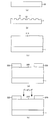
- FIG. 3 is a perspective view of the silicon substrate, channel layer, source electrode and drain electrode shown in FIGS. 1 and 2. It is sectional drawing which shows the structure of the plasma apparatus which manufactures the graphene which comprises the channel layer shown in FIG. 1, and the metal carbon nanowall thin film which comprises a source electrode and a drain electrode.
- FIG. 5 is a plan view of a planar conductor, a feeding electrode, and a termination electrode viewed from the matching circuit side shown in FIG. 4. It is sectional drawing of a planar conductor of a Y direction, and a figure which shows plasma density.
- FIG. 3 is a first process diagram illustrating a method for manufacturing the thin film transistor illustrated in FIGS. 1 and 2.
- FIG. 3 is a second process diagram illustrating a method of manufacturing the thin film transistor illustrated in FIGS. 1 and 2.
- FIG. 6 is a cross-sectional view illustrating a configuration of a thin film transistor according to a second embodiment.
- FIG. 10 is a plan view of the thin film transistor viewed from the A direction shown in FIG. 9.
- FIG. 11 is a first process diagram illustrating a method of manufacturing the thin film transistor illustrated in FIGS. 9 and 10.
- FIG. 11 is a second process diagram illustrating a method of manufacturing the thin film transistor illustrated in FIGS. 9 and 10.
- FIG. 11 is a third process diagram illustrating a method of manufacturing the thin film transistor illustrated in FIGS. 9 and 10.
- FIG. 6 is a cross-sectional view illustrating a configuration of a thin film transistor according to a third embodiment. It is the top view of the thin-film transistor seen from the A direction shown in FIG.
- FIG. 16 is a perspective view of the silicon substrate, channel layer, source electrode, and drain electrode shown in FIGS. 14 and 15.
- FIG. 16 is a process diagram illustrating a method of manufacturing the thin film transistor illustrated in FIGS. 14 and 15.
- FIG. 10 is a cross-sectional view showing a configuration of another thin film transistor according to Embodiment 3. It is the top view of the thin-film transistor seen from the A direction shown in FIG.
- FIG. 20 is a first process diagram illustrating a method of manufacturing the thin film transistor illustrated in FIGS. 18 and 19.
- FIG. 20 is a second process diagram illustrating the method of manufacturing the thin film transistor illustrated in FIGS. 18 and 19.
- FIG. 6 is a cross-sectional view illustrating a configuration of a thin film transistor according to a fourth embodiment.
- FIG. 23 is a plan view of the thin film transistor viewed from the A direction illustrated in FIG. 22.
- FIG. 24 is a first process diagram illustrating a method of manufacturing the thin film transistor illustrated in FIGS. 22 and 23.
- FIG. 24 is a second process diagram illustrating the method of manufacturing the thin film transistor illustrated in FIGS. 22 and 23.
- FIG. 10 is a cross-sectional view showing a configuration of another thin film transistor according to the fourth embodiment.
- FIG. 27 is a plan view of the thin film transistor viewed from the direction A shown in FIG. 26.
- FIG. 28 is a first process diagram illustrating a method of manufacturing the thin film transistor illustrated in FIGS. 26 and 27.
- FIG. 28 is a second process diagram illustrating the method of manufacturing the thin film transistor illustrated in FIGS. 26 and 27.
- FIG. 28 is a third process diagram illustrating the method of manufacturing the thin film transistor illustrated in FIGS. 26 and 27. It is the schematic of the conventional vertical type current drive device.
- FIG. 1 is a cross-sectional view showing a configuration of a thin film transistor according to Embodiment 1 of the present invention.
- 2 is a plan view of the thin film transistor viewed from the direction A shown in FIG.
- a thin film transistor 10 includes a silicon substrate 1, a channel layer 2, a source electrode 3, a drain electrode 4, an insulating film 5, and a gate electrode 6. With.
- the silicon substrate 1 is made of any one of n-type single crystal silicon, p-type single crystal silicon, n-type polycrystalline silicon, and p-type polycrystalline silicon.
- the silicon substrate 1 has a specific resistance of 0.1 to 1 ⁇ ⁇ cm, for example.
- the channel layer 2 is disposed on one main surface of the silicon substrate 1.
- the channel layer 2 is made of graphene and is disposed substantially perpendicular to the silicon substrate 1.
- graphene refers to a two-dimensional planar carbon sheet.
- the source electrode 3 is disposed in contact with one end of the channel layer 2 in the in-plane direction of the silicon substrate 1.
- the source electrode 3 is made of a metal carbon nanowall thin film.
- the drain electrode 4 is disposed in contact with the other end of the channel layer 2 so as to face the source electrode 3 in the in-plane direction of the silicon substrate 1.
- the drain electrode 4 is made of a metal carbon nanowall thin film.
- the metal carbon nanowall thin film refers to a carbon nanowall thin film having a linear current-voltage characteristic.
- the insulating film 5 is made of, for example, silicon dioxide (SiO 2 ).
- the insulating film 5 is disposed in contact with the surface of the silicon substrate 1 opposite to the one main surface where the channel layer 2 is disposed.
- the gate electrode 6 is disposed in contact with the insulating film 5.
- the gate electrode 6 has a laminated structure of Ti / Au, for example.
- the thickness of Ti is, for example, 10 nm
- the thickness of Au is, for example, 20 nm.
- FIG. 3 is a perspective view of the silicon substrate 1, the channel layer 2, the source electrode 3, and the drain electrode 4 shown in FIGS.
- silicon substrate 1 includes a convex portion 11 and a concave portion 12.
- the convex portion 11 and the concave portion 12 are formed on one main surface of the silicon substrate 1 along the direction DR1.
- the lengths of the convex portion 11 and the concave portion 12 in the direction DR1 may be the same as the length of the silicon substrate 1 or may be shorter than the length of the silicon substrate 1.
- the convex portions 11 and the concave portions 12 are alternately formed in the direction DR2 perpendicular to the direction DR1.
- the convex portion 11 has a length of 0.1 to 0.5 ⁇ m in the direction DR2.
- Recess 12 has a length of 0.6 to 1.5 ⁇ m in direction DR2.
- the convex portion 11 has a width of 0.1 to 0.5 ⁇ m
- the concave portion 12 has a width of 0.6 to 1.5 ⁇ m.
- the silicon substrate 1 has a concavo-convex shape arranged in a stripe shape on one main surface.
- the graphene has a thickness of 0.3 to 15 nm, a length of 5 to 10 ⁇ m (length in the direction DR1), and a height of 0.0003 to 10 ⁇ m.
- the graphene is arranged along the length direction of the protrusions 11 of the silicon substrate 1.
- the source electrode 3 is disposed on the convex portion 11 of the silicon substrate 1 so as to be in contact with the side surface 2A parallel to the thickness direction of the channel layer 2 (graphene).
- the drain electrode 4 is disposed on the convex portion 11 of the silicon substrate 1 so as to be in contact with the side surface 2B facing the side surface 2A parallel to the thickness direction of the channel layer 2 (graphene).
- the channel layer 2, the source electrode 3 and the drain electrode 4 are arranged linearly along the length direction (direction DR 1) of the convex portion 11 of the silicon substrate 1.
- the channel layer 2 is made of graphene and the source electrode 3 and the drain electrode 4 are made of a metal carbon nanowall thin film, the channel layer 2, the source electrode 3 and the drain electrode 4 are the same in which carbon atoms are arranged. Made of material. As a result, there is no potential barrier between the channel layer 2 and the source and drain electrodes 3 and 4.
- the drive voltage applied between the source electrode 3 and the drain electrode 4 in order to pass a current through the channel layer 2 can be lowered.
- the thin film transistor 10 is a thin film transistor using graphene as the channel layer 2.
- the thin film transistor 10 is a back gate type thin film transistor in which the gate electrode 6 is disposed below the channel layer 2.
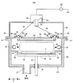
- FIG. 4 is a cross-sectional view showing the configuration of a plasma apparatus for producing the graphene constituting the channel layer 2 shown in FIG. 1 and the metal carbon nanowall thin film constituting the source electrode 3 and the drain electrode 4.
- the plasma apparatus 100 includes a vacuum vessel 20, a top plate 26, an exhaust port 27, a gas introduction unit 28, a holder 32, a heater 34, a shaft 36, a bearing unit 38, A mask 42, a partition plate 44, a planar conductor 50, a feeding electrode 52, a termination electrode 54, an insulating flange 56, packings 57 and 58, a shield box 60, a high frequency power supply 62, a matching circuit 64, Connection conductors 68 and 69 are provided.
- the vacuum vessel 20 is made of metal, and is connected to the vacuum exhaust device via the exhaust port 27.
- the vacuum vessel 20 is electrically connected to the ground node.
- the top plate 26 is disposed in contact with the vacuum vessel 20 so as to close the upper side of the vacuum vessel 20.
- a vacuum seal packing 57 is disposed between the vacuum vessel 20 and the top plate 26.
- the gas introduction unit 28 is disposed above the partition plate 44 in the vacuum vessel 20.
- the shaft 36 is fixed to the bottom surface of the vacuum vessel 20 via a bearing portion 38.
- the holder 32 is fixed to one end of the shaft 36.
- the heater 34 is disposed in the holder 32.
- the mask 42 is disposed on the holder 32 at the peripheral edge of the holder 32.
- the partition plate 44 is fixed to the side wall of the vacuum vessel 20 so as to close the space between the vacuum vessel 20 and the holder 32 above the holder 32.
- the feeding electrode 52 and the termination electrode 54 are fixed to the top plate 26 via an insulating flange 56.
- a vacuum seal packing 58 is disposed between the top plate 26 and the insulating flange 56.
- the planar conductor 50 is disposed so that both end portions in the X direction are in contact with the feeding electrode 52 and the termination electrode 54, respectively.
- the feeding electrode 52 and the termination electrode 54 have substantially the same length as the planar conductor 50 in the Y direction (direction perpendicular to the paper surface of FIG. 4) as will be described later.
- the feeding electrode 52 is connected to the output bar 66 of the matching circuit 64 by the connection conductor 68.
- the termination electrode 54 is connected to the shield box 60 via the connection conductor 69.
- the planar conductor 50, the feeding electrode 52, and the termination electrode 54 are made of, for example, copper and aluminum.
- the shield box 60 is disposed on the upper side of the vacuum vessel 20 and is in contact with the top plate 26.
- the high frequency power supply 62 is connected between the matching circuit 64 and the ground node.
- the matching circuit 64 is disposed on the shield box 60.
- connection conductors 68 and 69 have a plate shape having substantially the same length as that of the feeding electrode 52 and the termination electrode 54 in the Y direction.
- the gas introduction unit 28 supplies a gas 29 such as methane (CH 4 ) gas and hydrogen (H 2 ) gas supplied from a gas cylinder (not shown) into the vacuum container 20.
- the holder 32 supports the silicon substrate 1.
- the heater 34 heats the silicon substrate 1 to a desired temperature.
- the shaft 36 supports the holder 32.
- the mask 42 covers the peripheral edge of the silicon substrate 1. As a result, the product can be prevented from being formed on the peripheral edge of the silicon substrate 1.
- the partition plate 44 prevents the plasma 70 from reaching the holding mechanism of the silicon substrate 1.
- the feeding electrode 52 allows the high-frequency current supplied from the connection conductor 68 to flow through the planar conductor 50.
- the termination electrode 54 connects the end of the planar conductor 50 to the ground node directly or via a capacitor, and forms a closed loop of a high-frequency current from the high-frequency power source 62 to the planar conductor 50.
- the high frequency power supply 62 supplies high frequency power of 13.56 MHz to the matching circuit 64, for example.
- the matching circuit 64 supplies the high frequency power supplied from the high frequency power supply 62 to the connection conductor 68 while suppressing reflection.
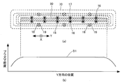
- FIG. 5 is a plan view of the planar conductor 50, the feeding electrode 52, and the termination electrode 54 as seen from the matching circuit 64 side shown in FIG.
- the planar conductor 50 has, for example, a rectangular planar shape and has sides 50 a and 50 b.
- the side 50a is longer than the side 50b.
- the side 50a is disposed along the X direction, and the side 50b is disposed along the Y direction.
- the feeding electrode 52 and the termination electrode 54 are disposed at both ends of the planar conductor 50 in the X direction along the side 50b of the planar conductor 50, respectively.
- the length in the Y direction of the feeding electrode 52 and the termination electrode 54 is close to the length of the side 50b parallel to the Y direction of the planar conductor 50 in order to flow the high-frequency current 16 as uniformly as possible in the Y direction (for example, It is preferable that the length is substantially the same as the length of the side 50b), but it may be slightly shorter or longer than the length of the side 50b.
- the lengths of the feeding electrode 52 and the termination electrode 54 in the Y direction may be set to 85% or more of the length of the side 50b.
- the power supply electrode 52 and the termination electrode 54 are formed of block-like electrodes, the high-frequency current 16 can flow through the planar conductor 50 almost uniformly in the Y direction.
- the high-frequency current When a high-frequency current is supplied to the planar conductor 50 using a dotted electrode, the high-frequency current does not flow uniformly through the planar conductor 50. In general, even when high-frequency power is supplied to a planar conductor and no plasma is present in the vicinity of the planar conductor, the high-frequency current is concentrated at the four corners of the cross section perpendicular to the conducting direction of the planar conductor due to the skin effect, etc. Flowing. This is because the high-frequency impedance distribution is small at the four corners of the planar conductor and large at other portions.
- FIG. 6 is a cross-sectional view of the planar conductor 50 in the Y direction and a diagram showing the plasma density.
- plasma 70 is generated in the vicinity of the planar conductor 50. That is, as shown in FIG. 6, when a high-frequency current 16 is passed through the planar conductor 50, a high-frequency magnetic field 17 is generated around the planar conductor 50, thereby generating an induced electric field 18 in the direction opposite to the high-frequency current 16. Electrons are accelerated by the induced electric field 18 to ionize the gas 29 (see FIG. 4) in the vicinity of the planar conductor 50, and a plasma 70 is generated in the vicinity of the planar conductor 50. An induced current 19 is induced in the plasma. It flows in the same direction as the electric field 18 (that is, the direction opposite to the high-frequency current 16).
- the high-frequency current 16 flowing through the planar conductor 50 is orthogonal to the energizing direction. It becomes uniform in the Y direction. The reason is as follows.
- the distribution of the high-frequency current 16 flowing in the planar conductor 50 becomes uniform in the Y direction.
- the high-frequency current 16 flows almost uniformly in the Y direction in the planar conductor 50. It becomes like this.
- the induced electric field 18 and the induced current 19 that are substantially uniformly distributed not only in the X direction, which is the energization direction, but also in the Y direction orthogonal to the X direction, in the vicinity of the surface on the plasma 70 generation side of the planar conductor 50.
- the induced electric field 18 can generate plasma with good uniformity over a wide area along the plane of the planar conductor 50.
- the plasma density distribution D1 is substantially uniform as shown in FIG.
- the plasma apparatus 100 generates inductively coupled plasma by flowing the high-frequency current 16 uniformly through the planar conductor 50.
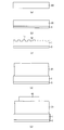
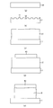
- FIGS. 7 and 8 are first and second process diagrams showing a method of manufacturing the thin film transistor 10 shown in FIGS. 1 and 2, respectively.
- the silicon substrate 1 as viewed from the B direction shown in FIG. 3 is shown.
- silicon substrate 30 made of n-type single crystal silicon is cleaned and degreased with ethanol or the like, and then silicon substrate 30 is cleaned with hydrofluoric acid (HF). (See step (a)). As a result, the surface of the silicon substrate 30 is terminated with hydrogen.
- HF hydrofluoric acid
- the back surface of the silicon substrate 30 is thermally oxidized to form the insulating film 5 made of SiO 2 (see step (b)).
- the thermal oxidation is performed, for example, by heat-treating the silicon substrate 30 at 1000 ° C. in an oxygen (O 2 ) gas atmosphere.
- a resist is applied to one main surface of the silicon substrate 30, the applied resist is patterned by electron beam lithography to form a resist pattern, and the silicon substrate is formed by reactive ion etching using the formed resist pattern as a mask.
- One main surface of 30 is etched.
- the silicon substrate 1 is placed on the holder 32 in the vacuum vessel 20 and the temperature of the silicon substrate 1 is raised to 600 ° C. or higher using the heater 34.
- the gas inlet 28 supplies 50 sccm CH 4 gas and 50 sccm of H 2 gas or a 100 sccm CH 4 gas, into the vacuum vessel 20. That is, a material gas containing carbon atoms is introduced into the vacuum vessel 20. And the pressure in the vacuum vessel 20 is adjusted to 1.33 Pa.
- the high frequency power supply 62 applies 1 kW high frequency power having a frequency of 13.56 MHz to the planar conductor 50 via the matching circuit 64 and the connection conductor 68.
- the plasma 70 is generated in the vacuum vessel 20 and the graphene 21 is formed on the convex portion 11 of the silicon substrate 1 in a self-organizing manner.
- the formation time of the graphene 21 is several minutes.
- the graphene 21 is manufactured using inductively coupled plasma.
- step (d) After step (d), a resist is applied on graphene 21, and the applied resist is patterned by photolithography to form a resist pattern 40 (see step (e)).
- step (e) graphene 21 is etched using resist pattern 40 as a mask (see step (f)). Thereby, the channel layer 2 made of graphene is formed.
- the sample is placed on the holder 32 in the vacuum vessel 20, and the silicon substrate 1 is heated to 600 ° C. or higher using the heater 34.
- Gas inlet 28 supplies 50 sccm CH 4 gas and 50 sccm of H 2 gas or a 100 sccm CH 4 gas, into the vacuum vessel 20. That is, a material gas containing carbon atoms is introduced into the vacuum vessel 20. And the pressure in the vacuum vessel 20 is adjusted to 1.33 Pa.
- the high frequency power supply 62 applies 1 kW high frequency power having a frequency of 13.56 MHz to the planar conductor 50 via the matching circuit 64 and the connection conductor 68.
- metal carbon nanowall thin films are formed on the convex portions 11 of the silicon substrate 1 in contact with the channel layer 2 in a self-organized manner.
- the formation time of the metal carbon nanowall thin film is 10 to 30 minutes.
- a metal carbon nanowall thin film 41 is formed on the resist pattern 40.
- the application of the high frequency power is stopped and the supply of CH 4 gas and H 2 gas (or CH 4 gas) is stopped.
- the source electrode 3 and the drain electrode 4 which consist of a metal carbon nanowall thin film are formed (refer process (g)).
- the metal carbon nanowall thin film which comprises the source electrode 3 and the drain electrode 4 is manufactured using inductively coupled plasma.
- the metal carbon nanowall thin film constituting the source electrode 3 and the drain electrode 4 has the same substrate temperature, material gas, high frequency power and reaction pressure as the substrate temperature, material gas, high frequency power and reaction pressure when the graphene 21 is formed. And the formation time is increased from several minutes to 10 to 30 minutes.
- step (g) the resist pattern 40 is removed using 1-methyl-2-pyrrolidone (see step (h)). Thereby, the metal carbon nanowall thin film 41 is removed by lift-off.
- step (i) the thin film transistor 10 is completed (see step (i)).
- the source electrode 3 and the drain electrode 4 are formed after the channel layer 2 is formed.
- the first embodiment is not limited to this, and the source electrode 3 is not limited thereto.
- the channel layer 2 may be formed after the drain electrode 4 is formed.
- the silicon substrate 1 has been described as having a concavo-convex shape formed in a stripe shape.
- the present invention is not limited to this, and the silicon substrate 1 is formed in a grid pattern. You may have uneven
- the grid-like uneven shape is formed by the same method as the stripe-like uneven shape.
- the thin film transistor 10 is manufactured using the silicon substrate 1 having a grid-like uneven shape, a grid-like uneven shape is formed on one main surface of the silicon substrate 1 in the step (c) shown in FIG.
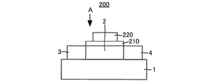
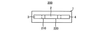
- FIG. 9 is a cross-sectional view showing the configuration of the thin film transistor according to the second embodiment.
- FIG. 10 is a plan view of the thin film transistor viewed from the direction A shown in FIG.
- thin film transistor 200 according to the second embodiment is obtained by replacing insulating film 5 of thin film transistor 10 shown in FIGS. 1 and 2 with insulating film 210 and replacing gate electrode 6 with gate electrode 220. Others are the same as those of the thin film transistor 10.
- the insulating film 210 is generally made of a dielectric, and is disposed on and in contact with the channel layer 2 above the channel layer 2.
- the dielectric is made of, for example, silicon oxide, barium titanate and ionic liquid.
- the gate electrode 220 is made of the same material as the gate electrode 6 described above, and is disposed on the insulating film 210 in contact with the insulating film 210.
- the thin film transistor 200 is a top gate type thin film transistor in which the gate electrode 220 is disposed above the channel layer 2.
- the channel layer 2 is made of graphene and the source electrode 3 and the drain electrode 4 are made of a metal carbon nanowall thin film, the channel layer 2, the source electrode 3 and the drain electrode 4 are the same in which carbon atoms are arranged. Made of material. As a result, there is no potential barrier between the channel layer 2 and the source and drain electrodes 3 and 4.
- the drive voltage applied between the source electrode 3 and the drain electrode 4 in order to pass a current through the channel layer 2 can be lowered.
- 11 to 13 are first to third process diagrams showing a method of manufacturing the thin film transistor 200 shown in FIGS. 9 and 10, respectively.
- the silicon substrate 1 as viewed from the B direction shown in FIG. 3 is shown.
- step (a) when the manufacture of thin film transistor 200 is started, the same step as step (a) shown in FIG. 7 is performed (see step (a)).
- steps (d), (e) shown in FIG. 7 and steps (f), (g), (h) shown in FIG. 8 are sequentially performed (steps (c) to (shown in FIG. 11).
- steps (f) and (g) shown in FIG. 8 are sequentially performed (steps (c) to (shown in FIG. 11).
- step (g) a resist is applied on channel layer 2, source electrode 3 and drain electrode 4, and the applied resist is patterned by photolithography and etching to form resist pattern 201. Form (see step (h)).
- an insulating film 210 is formed on the channel layer 2 using the resist pattern 201 as a mask (see step (i)).
- the insulating film 202 is formed on the resist pattern 201.
- resist pattern 201 is removed using 1-methyl-2-pyrrolidone (see step (j)). Thereby, the insulating film 202 is removed by lift-off.
- a resist is applied on the source electrode 3, the drain electrode 4, and the insulating film 210, and the applied resist is patterned by photolithography and etching to form a resist pattern 203 (see step (k)).
- Ti and Au are sequentially stacked on the insulating film 210 by electron beam evaporation using the resist pattern 203 as a mask, and the resist pattern 203 is removed using 1-methyl-2-pyrrolidone.
- the gate electrode 220 is formed on the insulating film 210, and the thin film transistor 200 is completed (see step (l)).
- the source electrode 3 and the drain electrode 4 are formed after the channel layer 2 is formed.
- the source electrode 3 is not limited thereto.
- the channel layer 2 may be formed after the drain electrode 4 is formed.
- the thin film transistor 200 includes the channel layer 2, the source electrode 3, and the drain electrode 4 having the same configuration as the thin film transistor 10.
- the drive voltage applied between the source electrode 3 and the drain electrode 4 in order to pass a current through the channel layer 2 can be lowered.
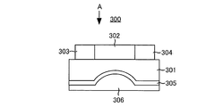
- FIG. 14 is a cross-sectional view showing the configuration of the thin film transistor according to the third embodiment.
- FIG. 15 is a plan view of the thin film transistor viewed from the direction A shown in FIG.
- the thin film transistor 300 includes a silicon substrate 301, a channel layer 302, a source electrode 303, a drain electrode 304, an insulating film 305, and a gate electrode 306. .
- the silicon substrate 301 has a convex portion 11 and a concave portion 12 formed in a stripe shape like the silicon substrate 1 on one main surface (see FIG. 3).
- the thickness of the region in contact with the channel layer 301 is thinner than the thickness of the region in contact with the source electrode 303 and the drain electrode 304.
- the other description of the silicon substrate 301 is the same as the description of the silicon substrate 1.
- the channel layer 302 is disposed on the convex portion 11 along the length direction of the convex portion 11 of the silicon substrate 301.
- the channel layer 302 is made of a carbon nanowall thin film and is arranged substantially perpendicular to the silicon substrate 301.
- the carbon nanowall thin film refers to a thin film having a structure in which a plurality of graphenes are stacked, and indicates a semiconductor characteristic.
- the semiconductor characteristic is a characteristic that the drain-source current changes depending on the gate voltage.
- the source electrode 303 is disposed in contact with the channel layer 302 on one end side of the channel layer 302 in the in-plane direction of the silicon substrate 301.
- the source electrode 303 is made of a metal carbon nanowall thin film.
- the drain electrode 304 is disposed in contact with the channel layer 302 on the other end side of the channel layer 302 so as to face the source electrode 303 in the in-plane direction of the silicon substrate 301.
- the drain electrode 304 is made of a metal carbon nanowall thin film.
- the insulating film 305 is disposed in contact with the back surface of the silicon substrate 301 (the surface opposite to the surface on which the channel layer 302 is formed).
- the other description of the insulating film 305 is the same as the description of the insulating film 5.
- the gate electrode 306 is disposed in contact with the insulating film 305.
- the other description of the gate electrode 306 is the same as the description of the gate electrode 6.
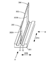
- FIG. 16 is a perspective view of the silicon substrate 301, the channel layer 302, the source electrode 303, and the drain electrode 304 shown in FIG. 14 and FIG.
- the carbon nanowall thin film has a thickness of 10 to 15 nm, a length of 5 to 10 ⁇ m (length in the direction DR1), and a height of 60 to 2500 nm.
- the carbon nanowall thin films are arranged along the length direction of the convex portions 11 of the silicon substrate 301.
- the source electrode 303 is formed on the convex portion 11 of the silicon substrate 301 integrally with the channel layer 302 in contact with the side surface 302A parallel to the thickness direction of the channel layer 302 (carbon nanowall thin film).
- the drain electrode 304 is formed on the convex portion 11 of the silicon substrate 301 integrally with the channel layer 302 in contact with the side surface 302B facing the side surface 302A parallel to the thickness direction of the channel layer 302 (carbon nanowall thin film).
- the channel layer 302, the source electrode 303, and the drain electrode 304 are integrally formed along the length direction (direction DR1) of the convex portion 11 of the silicon substrate 301.
- the source electrode 303, and the drain electrode 304 are integrally formed, between the channel layer 302 and the source electrode 303, and between the channel layer 302 and the drain electrode.
- a dotted line indicates the area 304.
- the channel layer 302 is made of a carbon nanowall thin film
- the source electrode 303 and the drain electrode 304 are made of a metal carbon nanowall thin film
- the channel layer 302, the source electrode 303, and the drain electrode 304 are integrally formed. There is no potential barrier between the channel layer 302 and the source and drain electrodes 303 and 304.
- the driving voltage applied between the source electrode 303 and the drain electrode 304 in order to pass a current through the channel layer 302 can be lowered.
- the thin film transistor 300 is a thin film transistor using a carbon nanowall thin film as the channel layer 302.
- the thin film transistor 300 is a back-gate thin film transistor as in the thin film transistor 10.
- FIG. 17 is a process diagram showing a method of manufacturing the thin film transistor 300 shown in FIGS. 14 and 15.
- FIG. 17C two side views of the silicon substrate 301 viewed from the A direction and the B direction shown in FIG. 16 are shown.
- the silicon substrate 301 viewed from the direction B shown in FIG. 16 is shown.
- steps (a) and (c) shown in FIG. 7 are executed to form silicon substrate 1 (steps (a) and (c). b)).
- a resist is applied to the back surface of the silicon substrate 1, the applied resist is patterned by photolithography and etching, and a resist pattern is formed so as to cover the region of the silicon substrate 1 facing the source electrode 303 and the drain electrode 304. To do. Then, using the formed resist pattern as a mask, the back surface side of the silicon substrate 1 is etched to form a recess 3011. Thereby, the silicon substrate 301 is formed (see step (c)).
- step (d) Thereafter, the resist pattern is removed, and the back surface of the silicon substrate 301 is oxidized at a temperature of 1000 ° C. in an O 2 gas atmosphere to form an insulating film 305 (see step (d)).
- the silicon substrate 301 / insulating film 305 is placed on the holder 32 in the vacuum vessel 20, and the temperature of the silicon substrate 301 / insulating film 305 is raised to 600 ° C. or higher using the heater.
- the region 301A of the silicon substrate 301 facing the concave portion 3012 is not heated to 600 ° C. or higher, and is set to 400 to 500 ° C. and is adjacent to the region 301A.
- the two regions 301B and 301C are set to 600 ° C. or higher.
- the gas inlet 28 supplies 50 sccm CH 4 gas and 50 sccm of H 2 gas or a 100 sccm CH 4 gas, into the vacuum vessel 20. That is, a material gas containing carbon atoms is introduced into the vacuum vessel 20. And the pressure in the vacuum vessel 20 is adjusted to 1.33 Pa.
- the high frequency power supply 62 applies 1 kW high frequency power having a frequency of 13.56 MHz to the planar conductor 50 via the matching circuit 64 and the connection conductor 68.
- plasma 70 is generated in the vacuum vessel 20, and a carbon nanowall thin film and a metal carbon nanowall thin film are formed on the convex portion 11 of the silicon substrate 301 in a self-organizing manner.
- a carbon nanowall thin film is formed on the region 301A of the silicon substrate 301, and a metal carbon nanowall thin film is formed on the two regions 301B and 301C. That is, the channel layer 302 made of a carbon nanowall thin film, and the source electrode 303 and the drain electrode 304 made of a metal carbon nanowall thin film are integrally formed (see step (e)).
- the formation time of the carbon nanowall thin film and the metal carbon nanowall thin film is 10 to 30 minutes.
- the carbon nanowall thin film and the metal carbon nanowall thin film are manufactured using inductively coupled plasma.
- step (e) the same step as step (i) shown in FIG. 8 is performed to form gate electrode 306 in contact with insulating film 305.
- step (f) the thin film transistor 300 is completed (see step (f)).
- the channel layer 302, the source electrode 303, and the drain electrode 304 are integrally formed in one process, and thus, between the channel layer 302, the source electrode 303, and the drain electrode 304, There is no potential barrier at all.
- the driving voltage for flowing current through the channel layer 302 can be very low.
- the number of processes is smaller than that of the thin film transistors 10 and 200.
- the thin film transistor 300 can be manufactured by a number.
- FIG. 18 is a cross-sectional view showing the configuration of another thin film transistor according to the third embodiment.
- FIG. 19 is a plan view of the thin film transistor viewed from the direction A shown in FIG.
- the thin film transistor according to Embodiment 3 may be the thin film transistor 300A shown in FIGS.
- silicon substrate 301, insulating film 305 and gate electrode 306 of thin film transistor 300 shown in FIGS. 14 and 15 are replaced with silicon substrate 1, insulating film 5 and gate electrode 6, respectively. Others are the same as those of the thin film transistor 300.
- the channel layer 302, the source electrode 303, and the drain electrode 304 are integrally formed on the convex portion 11 along the length direction of the convex portion 11 of the silicon substrate 1.
- the silicon substrate 1, the insulating film 5, and the gate electrode 6 are as described in FIGS. Therefore, the gate electrode 6 is disposed below the channel layer 302.
- the thin film transistor 300A is a back-gate thin film transistor, like the thin film transistor 10.
- 20 and 21 are first and second process diagrams showing a method of manufacturing the thin film transistor 300A shown in FIGS. 18 and 19, respectively.
- the silicon substrate 1 viewed from the direction B shown in FIG. 3 is shown.
- the silicon substrate 1 / insulating film 5 is placed on the holder 32 in the vacuum vessel 20 and the temperature of the silicon substrate 1 / insulating film 5 is raised to 600 ° C. or higher using the heater 34.
- the gas inlet 28 supplies 50 sccm CH 4 gas and 50 sccm of H 2 gas or a 100 sccm CH 4 gas, into the vacuum vessel 20. That is, a material gas containing carbon atoms is introduced into the vacuum vessel 20. And the pressure in the vacuum vessel 20 is adjusted to 1.33 Pa.
- the high frequency power supply 62 applies 1 kW high frequency power having a frequency of 13.56 MHz to the planar conductor 50 via the matching circuit 64 and the connection conductor 68.
- the metal carbon nanowall thin film 310 is formed in a self-organized manner on the convex portion 11 of the silicon substrate 1 (see step (d)).
- the formation time of the metal carbon nanowall thin film 310 is 10 to 30 minutes.
- the metal carbon nanowall thin film 310 is manufactured using inductively coupled plasma.
- step (d) a resist is applied on metal carbon nanowall thin film 310, and the applied resist is patterned by photolithography and etching to form resist pattern 320 (see step (e)).
- step (e) dopant is doped into metal carbon nanowall thin film 310 by plasma CVD using resist pattern 320 as a mask (see step (f)).
- the dopant is composed of iodine, carbon dioxide, an inert element, or boron.
- Iodine enters the skeleton of the carbon array constituting the metal carbon nanowall thin film 310.
- Carbon dioxide is adsorbed on the surface of the metal carbon nanowall thin film 310.
- the inert element is made of, for example, Ar, and generates a defect in the metal carbon nanowall thin film 310.
- Boron also generates defects in the metal carbon nanowall thin film 310, like the inert element.
- the metal carbon nanowall thin film 310 becomes a carbon nanowall thin film having semiconductor characteristics.
- step (f) the resist pattern 320 is removed using 1-methyl-2-pyrrolidone.
- a channel layer 302 made of a carbon nanowall thin film, and a source electrode 303 and a drain electrode 304 made of a metal carbon nanowall thin film are formed (see step (g)).
- step (h) the same process as the process (i) shown in FIG. 8 is performed to form the gate electrode 6 in contact with the insulating film 5.
- the thin film transistor 300A is completed (see step (h)).
- the channel layer 302 A source electrode 303 and a drain electrode 304 are formed (see steps (f) and (g)).
- the channel layer 302, the source electrode 303, and the drain electrode 304 are made of the same material in which carbon atoms are arranged, there is no potential barrier between the channel layer 302, the source electrode 303, and the drain electrode 304. No longer exists.
- the driving voltage for flowing current through the channel layer 302 can be very low.
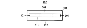
- FIG. 22 is a cross-sectional view showing the configuration of the thin film transistor according to the fourth embodiment.
- FIG. 23 is a plan view of the thin film transistor viewed from the direction A shown in FIG.
- thin film transistor 400 according to the fourth embodiment is obtained by replacing insulating film 305 and gate electrode 306 of thin film transistor 300 shown in FIGS. 14 and 15 with insulating film 410 and gate electrode 420, respectively. Others are the same as those of the thin film transistor 300.
- the insulating film 410 is disposed on the channel layer 302 in contact with the channel layer 302 on the opposite side of the channel layer 302 from the silicon substrate 301 side.
- the insulating film 410 is made of the same material as the insulating film 210 (see FIG. 9).
- the gate electrode 420 is disposed on the insulating film 410 in contact with the insulating film 410.
- the gate electrode 420 is made of the same material as the gate electrode 6.
- the gate electrode 420 is disposed on the upper side of the channel layer 302. Accordingly, the thin film transistor 400 is a top-gate thin film transistor.
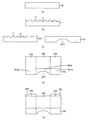
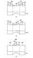
- FIGS. 24 and 25 are first and second process diagrams showing a method of manufacturing the thin film transistor 400 shown in FIGS. 22 and 23, respectively. Note that, in step (c) of FIG. 24, two side views of the silicon substrate 301 viewed from the A direction and the B direction shown in FIG. 16 are shown. Further, in steps (d) to (h), the silicon substrate 301 viewed from the direction B shown in FIG. 16 is shown.
- steps (a) to (c) shown in FIG. 17 are performed to form silicon substrate 301 (steps (a) to (a) to (a) Step (c)).
- a resist is applied on the channel layer 302, the source electrode 303, and the drain electrode 304, and the applied resist is patterned by photolithography and etching to form a resist pattern 430 on the source electrode 303 and the drain electrode 304 (see FIG. Step (e)).
- step (e) insulating film 410 is formed on channel layer 302 using resist pattern 430 as a mask (see step (f)).
- the insulating film 450 is formed on the resist pattern 430.
- the resist pattern 430 is removed using 1-methyl-2-pyrrolidone. Thereby, the insulating film 450 is removed by lift-off.
- a resist is applied onto the source electrode 303, the drain electrode 304, and the insulating film 410, and the applied resist is patterned by photolithography and etching, so that the resist pattern 460 is formed into the source electrode 303, the drain electrode 304, and the insulating film 410. (See step (g)).
- the thin film transistor 400 is completed (see step (h)).
- the channel layer 302, the source electrode 303, and the drain electrode 304 are integrally formed in one step (see step (d)); therefore, the channel layer 302, the source electrode 303, and the drain are formed. There is no potential barrier between the electrode 304 and the electrode 304.
- the driving voltage for flowing current through the channel layer 302 can be very low.
- the channel layer 302, the source electrode 303, and the drain electrode 304 are formed at the same time in one step (see step (d)), and therefore, compared with the thin film transistors 10 and 200.
- the thin film transistor 400 can be manufactured with a small number of steps.
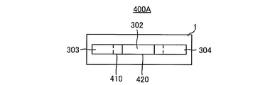
- FIG. 26 is a cross-sectional view showing the configuration of another thin film transistor according to the fourth embodiment.
- FIG. 27 is a plan view of the thin film transistor viewed from the A direction shown in FIG.
- the thin film transistor according to the fourth embodiment may be a thin film transistor 400A shown in FIGS.
- thin film transistor 400A is the same as thin film transistor 400 except that silicon substrate 301 of thin film transistor 400 shown in FIGS. 22 and 23 is replaced with silicon substrate 1.
- the channel layer 302, the source electrode 303, and the drain electrode 304 are integrally formed on the convex portion 11 along the length direction of the convex portion 11 of the silicon substrate 1.
- the silicon substrate 1 is as described above.
- the gate electrode 420 is disposed above the channel layer 302. Accordingly, the thin film transistor 400A is a top-gate thin film transistor.
- steps (a) and (b) shown in FIG. 24 are executed to form silicon substrate 1 (steps (a) and (b). )reference).
- step (b) the same step as the step (d) shown in FIG. 20 is performed to form the metal carbon nanowall thin film 310 on the silicon substrate 1 (see step (c)).
- step (e) shown in FIG. 20 and steps (f) and (g) shown in FIG. 21 are performed to form channel layer 302, source electrode 303 and drain electrode 304 on silicon substrate 1 ( Steps (d) and (e) in FIG. 28 and step (f) in FIG. 29).
- the insulating film 410 and the gate electrode 420 are formed by executing the same process as the process (e) shown in FIG. 24 and the processes (f), (g), and (h) shown in FIG.
- the thin film transistor 400A is completed (see steps (g), (h), (i) in FIG. 29 and step (j) in FIG. 30).
- the channel layer 302 A source electrode 303 and a drain electrode 304 are formed (see steps (e) and (f)).
- the channel layer 302, the source electrode 303, and the drain electrode 304 are made of the same material in which carbon atoms are arranged, there is no potential barrier between the channel layer 302, the source electrode 303, and the drain electrode 304. not exist.
- the driving voltage for flowing current through the channel layer 302 can be very low.
- the back gate type thin film transistor 10 including the channel layer 2 made of graphene and the source electrode 3 and the drain electrode 4 made of a metal carbon nanowall thin film has been described.
- the top gate type thin film transistor 200 including the channel layer 2 made of graphene and the source electrode 3 and the drain electrode 4 made of a metal carbon nanowall thin film has been described.
- the back gate type thin film transistors 300 and 300A including the channel layer 302 made of a carbon nanowall thin film and the source electrode 303 and the drain electrode 304 made of a metal carbon nanowall thin film have been described.
- the top-gate thin film transistors 400 and 400A including the channel layer 302 made of a carbon nanowall thin film and the source electrode 303 and the drain electrode 304 made of a metal carbon nanowall thin film have been described.
- the thin film transistor according to the embodiment of the present invention is arranged on the convex part along the length direction of the convex part of the concave and convex shape, and the silicon substrate in which the concave and convex shape is formed in a stripe shape or a grid pattern on one main surface.
- the channel layer, the source electrode, and the drain electrode are made of the same material in which carbon atoms are arranged, there is no potential barrier between the channel layer, the source electrode, and the drain electrode. This is because the driving voltage applied between the channel layer and the source and drain electrodes can be lowered.
- a thin film transistor manufacturing method is a thin film transistor manufacturing method using a carbon nanowall thin film as a channel layer, and a concavo-convex shape is formed in a stripe shape or a grid shape on one main surface of a silicon substrate.
- a first step of forming, a carbon nanowall thin film serving as a channel layer, a first metal carbon nanowall thin film serving as a source electrode, and a second metal carbon nanowall thin film serving as a drain electrode are formed in an uneven shape.
- the method of manufacturing a thin film transistor according to the embodiment of the present invention is a method of manufacturing a thin film transistor using a carbon nanowall thin film as a channel layer, wherein the concavo-convex shape is formed in a stripe shape or a grid pattern on one main surface of the silicon substrate.
- a third step of forming an electrode on the convex portion, and a carbon nano-wall of the channel layer A fourth step of forming a facing to the insulating film Le thin, it is sufficient that a fifth step of forming a gate electrode in contact with the insulating film.
- the channel layer, the source electrode, and the drain electrode can be made of the same material in which carbon atoms are arranged, and are applied between the channel layer, the source electrode, and the drain electrode in order to pass a current through the channel layer. This is because the driving voltage can be lowered.
- the present invention is applied to a thin film transistor and a manufacturing method thereof.
Landscapes
- Chemical & Material Sciences (AREA)
- Engineering & Computer Science (AREA)
- Materials Engineering (AREA)
- Nanotechnology (AREA)
- Thin Film Transistor (AREA)
- Electroluminescent Light Sources (AREA)
- Insulated Gate Type Field-Effect Transistor (AREA)
Abstract
薄膜トランジスタ10は、シリコン基板1と、チャネル層2と、ソース電極3と、ドレイン電極4と、絶縁膜5と、ゲート電極6とを備える。チャネル層2、ソース電極3およびドレイン電極4は、シリコン基板1の凹凸形状の凸部の長さ方向に沿って凸部上に直線状に配置される。チャネル層2は、カーボンナノウォール薄膜からなり、ソース電極3およびドレイン電極4は、金属カーボンナノウォール薄膜からなる。絶縁膜5は、SiO2からなり、シリコン基板1の裏面に接して配置される。ゲート電極6は、Ti/Auの積層構造からなり、絶縁膜5に接して配置される。
Description
この発明は、薄膜トランジスタおよびその製造方法に関するものである。
従来、カーボンナノウォールを用いた縦型電流駆動デバイスが知られている(特許文献1)。
図31は、従来の縦型電流駆動デバイスの概略図である。図31を参照して、従来の縦型電流駆動デバイス500は、カーボンナノウォール501と、ソース電極502と、ドレイン電極503と、ゲート電極504とを備える。
カーボンナノウォール501は、数層のグラフェンシートが積層された構造からなる。
ソース電極502は、カーボンナノウォール501の一方端に配置され、ドレイン電極503は、カーボンナノウォール501の頂部においてカーボンナノウォール401の最表面または最下面に接して配置される。ゲート電極504は、カーボンナノウォール501の最表面に接して配置される。
特開2006-272491号公報
しかし、特許文献1には、ソース電極およびドレイン電極がチャネル層と同じ材料からなることが記載されていないため、縦型電流駆動デバイスの駆動電圧を低くすることが困難であるという問題がある。
そこで、この発明は、かかる問題を解決するためになされたものであり、その目的は、駆動電圧の低減が可能な薄膜トランジスタを提供することである。
また、この発明の別の目的は、駆動電圧の低減が可能な薄膜トランジスタの製造方法を提供することである。
この発明の実施の形態によれば、薄膜トランジスタは、シリコン基板と、チャネル層と、ソース電極と、ドレイン電極と、ゲート電極と、絶縁膜とを備える。シリコン基板は、一主面に凹凸形状がストライプ状または碁盤目状に形成される。チャネル層は、凹凸形状の凸部の長さ方向に沿って凸部上に配置され、シリコン基板の法線方向に成長したグラフェンまたはカーボンナノウォール薄膜からなる。ソース電極は、グラフェンまたはカーボンナノウォール薄膜においてグラフェンまたはカーボンナノウォール薄膜の厚み方向に平行な第1の側面に接し、金属カーボンナノウォール薄膜からなる。ドレイン電極は、グラフェンまたはカーボンナノウォール薄膜の面内方向においてソース電極に対向するように配置され、グラフェンまたはカーボンナノウォール薄膜において第1の側面に対向する第2の側面に接し、金属カーボンナノウォール薄膜からなる。絶縁膜は、グラフェンまたはカーボンナノウォール薄膜とゲート電極との間に配置される。
また、この発明の実施の形態によれば、薄膜トランジスタの製造方法は、カーボンナノウォール薄膜をチャネル層として用いた薄膜トランジスタの製造方法であって、シリコン基板の一主面に凹凸形状をストライプ状または碁盤目状に形成する第1の工程と、チャネル層となるカーボンナノウォール薄膜と、ソース電極となる第1の金属カーボンナノウォール薄膜と、ドレイン電極となる第2の金属カーボンナノウォール薄膜とを、凹凸形状の凸部の長さ方向に沿って凸部上に同時に形成する第2の工程と、チャネル層のカーボンナノウォール薄膜に対向して絶縁膜を形成する第3の工程と、絶縁膜に接してゲート電極を形成する第4の工程とを備える。
更に、この発明の実施の形態によれば、薄膜トランジスタの製造方法は、カーボンナノウォール薄膜をチャネル層として用いた薄膜トランジスタの製造方法であって、シリコン基板の一主面に凹凸形状をストライプ状または碁盤目状に形成する第1の工程と、金属カーボンナノウォール薄膜を凹凸形状の凸部の長さ方向に沿って前記凸部上に形成する第2の工程と、金属カーボンナノウォール薄膜の一部分にドーパントをドーピングして一部分を半導体特性を有するカーボンナノウォール薄膜に変化させ、カーボンナノウォール薄膜からなるチャネル層と、第1の金属カーボンナノウォール薄膜からなるソース電極と、第2の金属カーボンナノウォール薄膜からなるドレイン電極とを凸部上に形成する第3の工程と、チャネル層のカーボンナノウォール薄膜に対向して絶縁膜を形成する第4の工程と、絶縁膜に接してゲート電極を形成する第5の工程とを備える。
この発明の実施の形態による薄膜トランジスタにおいては、チャネル層、ソース電極およびドレイン電極は、炭素原子が配列された同じ材料からなる。その結果、チャネル層と、ソース電極およびドレイン電極との間に電位的な障壁及び接触抵抗が無い。
従って、チャネル層に電流を流すためにソース電極とドレイン電極との間に印加する駆動電圧及び損失を低くできる。
また、この発明の実施の形態による薄膜トランジスタの製造方法は、カーボンナノウォール薄膜をチャネル層として用いた薄膜トランジスタの製造方法であって、チャネル層となるカーボンナノウォール薄膜と、ソース電極となる第1の金属カーボンナノウォール薄膜と、ドレイン電極となる第2の金属カーボンナノウォール薄膜とを同時に形成する。
従って、駆動電圧の低い薄膜トランジスタを製造できる。また、工程数を少なくして薄膜トランジスタを製造できる。
更に、この発明の実施の形態による薄膜トランジスタの製造方法は、カーボンナノウォール薄膜をチャネル層として用いた薄膜トランジスタの製造方法であって、金属カーボンナノウォール薄膜の一部分をカーボンナノウォール薄膜に変えてカーボンナノウォール薄膜からなるチャネル層と、第1の金属カーボンナノウォール薄膜からなるソース電極と、第2の金属カーボンナノウォール薄膜からなるドレイン電極とを形成する。
従って、駆動電圧の低い薄膜トランジスタを製造できる。また、チャネル層、ソース電極およびドレイン電極を形成する工程数を少なくして薄膜トランジスタを製造できる。
本発明の実施の形態について図面を参照しながら詳細に説明する。なお、図中同一または相当部分には同一符号を付してその説明は繰返さない。
[実施の形態1]
図1は、この発明の実施の形態1による薄膜トランジスタの構成を示す断面図である。また、図2は、図1に示すA方向から見た薄膜トランジスタの平面図である。
図1は、この発明の実施の形態1による薄膜トランジスタの構成を示す断面図である。また、図2は、図1に示すA方向から見た薄膜トランジスタの平面図である。
図1および図2を参照して、この発明の実施の形態1による薄膜トランジスタ10は、シリコン基板1と、チャネル層2と、ソース電極3と、ドレイン電極4と、絶縁膜5と、ゲート電極6とを備える。
シリコン基板1は、n型単結晶シリコン、p型単結晶シリコン、n型多結晶シリコンおよびp型多結晶シリコンのいずれかからなる。そして、シリコン基板1は、例えば、0.1~1Ω・cmの比抵抗を有する。
チャネル層2は、シリコン基板1の一主面上に配置される。そして、チャネル層2は、グラフェンからなり、シリコン基板1に略垂直に配置される。
なお、この明細書においては、グラフェンとは、2次元の平面状炭素シートを言う。
ソース電極3は、シリコン基板1の面内方向において、チャネル層2の一方端に接して配置される。そして、ソース電極3は、金属カーボンナノウォール薄膜からなる。ドレイン電極4は、シリコン基板1の面内方向において、ソース電極3に対向するようにチャネル層2の他方端に接して配置される。そして、ドレイン電極4は、金属カーボンナノウォール薄膜からなる。
なお、この明細書においては、金属カーボンナノウォール薄膜とは、電流-電圧特性が直線状のカーボンナノウォール薄膜を言う。
絶縁膜5は、例えば、二酸化シリコン(SiO2)からなる。そして、絶縁膜5は、シリコン基板1のチャネル層2が配置された一主面と反対側の表面に接して配置される。
ゲート電極6は、絶縁膜5に接して配置される。そして、ゲート電極6は、例えば、Ti/Auの積層構造からなる。この場合、Tiの厚みは、例えば、10nmであり、Auの厚みは、例えば、20nmである。
図3は、図1および図2に示すシリコン基板1、チャネル層2、ソース電極3およびドレイン電極4の斜視図である。
図3を参照して、シリコン基板1は、凸部11と凹部12とを含む。凸部11および凹部12は、方向DR1に沿ってシリコン基板1の一主面に形成される。方向DR1における凸部11および凹部12の長さは、シリコン基板1の長さと同じであっても、シリコン基板1の長さよりも短くてもよい。凸部11および凹部12は、方向DR1に垂直な方向DR2において、交互に形成される。凸部11は、方向DR2において、0.1~0.5μmの長さを有する。凹部12は、方向DR2において、0.6~1.5μmの長さを有する。即ち、凸部11は、0.1~0.5μmの幅を有し、凹部12は、0.6~1.5μmの幅を有する。また、凸部11の高さ(=凹部12の深さ)は、0.3~0.6μmである。
このように、シリコン基板1は、ストライプ状に配置された凹凸形状を一主面に有する。
チャネル層2を構成するグラフェンは、シリコン基板1の凸部11の長さ方向(=方向DR1)に沿って凸部11上に形成される。
そして、グラフェンは、0.3~15nmの厚み、5~10μmの長さ(方向DR1における長さ)および0.0003~10μmの高さを有する。
このように、グラフェンは、シリコン基板1の凸部11の長さ方向に沿って配列される。
ソース電極3は、チャネル層2(グラフェン)の厚み方向に平行な側面2Aに接するようにシリコン基板1の凸部11上に配置される。
ドレイン電極4は、チャネル層2(グラフェン)の厚み方向に平行な側面2Aに対向する側面2Bに接するようにシリコン基板1の凸部11上に配置される。
このように、チャネル層2、ソース電極3およびドレイン電極4は、シリコン基板1の凸部11の長さ方向(方向DR1)に沿って直線状に配置される。
所望の電圧をゲート電極6に印加すると、チャネル層2を構成するグラフェンのシリコン基板1側に電子または正孔が誘起される。そして、電子または正孔が誘起された状態で所望の電圧をソース電極3とドレイン電極4との間に印加すると、グラフェンの電子または正孔が誘起された領域を介して、電流がソース電極3とドレイン電極4との間に流れる。この場合、ソース電極3とドレイン電極4との間に流れる電流値は、ゲート電極6に印加される電圧によって制御される。
薄膜トランジスタ10においては、チャネル層2がグラフェンからなり、ソース電極3およびドレイン電極4が金属カーボンナノウォール薄膜からなるので、チャネル層2、ソース電極3およびドレイン電極4は、炭素原子が配列された同じ材料からなる。その結果、チャネル層2とソース電極3およびドレイン電極4との間に電位的な障壁が存在しない。
従って、チャネル層2に電流を流すためにソース電極3とドレイン電極4との間に印加する駆動電圧を低くできる。
このように、薄膜トランジスタ10は、グラフェンをチャネル層2として用いた薄膜トランジスタである。また、薄膜トランジスタ10は、ゲート電極6がチャネル層2の下側に配置されたバックゲート型の薄膜トランジスタである。
図4は、図1に示すチャネル層2を構成するグラフェンと、ソース電極3およびドレイン電極4を構成する金属カーボンナノウォール薄膜とを製造するプラズマ装置の構成を示す断面図である。図4を参照して、プラズマ装置100は、真空容器20と、天板26と、排気口27と、ガス導入部28と、ホルダ32と、ヒータ34と、軸36と、軸受部38と、マスク42と、仕切り板44と、平面導体50と、給電電極52と、終端電極54と、絶縁フランジ56と、パッキン57,58と、シールドボックス60と、高周波電源62と、整合回路64と、接続導体68,69とを備える。
真空容器20は、金属製であり、排気口27を介して真空排気装置に接続される。また、真空容器20は、電気的に接地ノードに接続される。天板26は、真空容器20の上側を塞ぐように真空容器20に接して配置される。この場合、真空容器20と天板26との間には、真空シール用のパッキン57が配置される。
ガス導入部28は、真空容器20内において仕切り板44よりも上側に配置される。軸36は、軸受部38を介して真空容器20の底面に固定される。ホルダ32は、軸36の一方端に固定される。ヒータ34は、ホルダ32内に配置される。マスク42は、ホルダ32の周縁部においてホルダ32上に配置される。仕切り板44は、ホルダ32よりも上側において真空容器20とホルダ32との間を塞ぐように真空容器20の側壁に固定される。
給電電極52および終端電極54は、絶縁フランジ56を介して天板26に固定される。この場合、天板26と絶縁フランジ56との間には、真空シール用のパッキン58が配置される。
平面導体50は、X方向における両端部がそれぞれ給電電極52および終端電極54に接するように配置される。
給電電極52および終端電極54は、後述するようにY方向(図4の紙面に垂直な方向)において平面導体50とほぼ同じ長さを有する。そして、給電電極52は、接続導体68によって整合回路64の出力バー66に接続される。終端電極54は、接続導体69を介してシールドボックス60に接続される。平面導体50、給電電極52および終端電極54は、例えば、銅およびアルミニウム等からなる。
シールドボックス60は、真空容器20の上側に配置され、天板26に接する。高周波電源62は、整合回路64と接地ノードとの間に接続される。整合回路64は、シールドボックス60上に配置される。
接続導体68,69は、Y方向において給電電極52および終端電極54とほぼ同じ長さを有する板形状からなる。
ガス導入部28は、ガスボンベ(図示せず)から供給されたメタン(CH4)ガスおよび水素(H2)ガス等のガス29を真空容器20内に供給する。ホルダ32は、シリコン基板1を支持する。ヒータ34は、シリコン基板1を所望の温度に加熱する。軸36は、ホルダ32を支持する。マスク42は、シリコン基板1の周縁部を覆う。これによって、生成物がシリコン基板1の周縁部に形成されるのを防止できる。仕切り板44は、プラズマ70がシリコン基板1の保持機構に達するのを防止する。
給電電極52は、接続導体68から供給された高周波電流を平面導体50に流す。終端電極54は、平面導体50の端部を直接またはキャパシタを介して接地ノードに接続し、高周波電源62から平面導体50にかけて高周波電流の閉ループを作る。
高周波電源62は、例えば、13.56MHzの高周波電力を整合回路64へ供給する。整合回路64は、高周波電源62から供給された高周波電力を反射を抑制して接続導体68に供給する。
図5は、図4に示す整合回路64側から見た平面導体50、給電電極52および終端電極54の平面図である。図5を参照して、平面導体50は、例えば、長方形の平面形状からなり、辺50a,50bを有する。辺50aは、辺50bよりも長い。そして、辺50aは、X方向に沿って配置され、辺50bは、Y方向に沿って配置される。
給電電極52および終端電極54は、それぞれ、平面導体50の辺50bに沿って平面導体50のX方向の両端部に配置される。給電電極52および終端電極54のY方向の長さは、高周波電流16をY方向においてできる限り一様に流すために、平面導体50のY方向に平行な辺50bの長さに近づける(例えば、辺50bの長さと実質的に同じにする)のが好ましいが、辺50bの長さよりも幾分短くてもよいし、長くてもよい。数値で表せば、給電電極52および終端電極54のY方向の長さは、辺50bの長さの85%以上の長さに設定すればよい。
このように、給電電極52および終端電極54は、ブロック状の電極からなるので、Y方向において平面導体50にほぼ一様に高周波電流16を流すことができる。
平面導体50に点状の電極を用いて高周波電流を供給した場合、高周波電流は、平面導体50を一様に流れない。一般的に、平面導体に高周波電力を供給しても、平面導体の近傍にプラズマが存在しない状態では、表皮効果等によって、高周波電流は、平面導体の通電方向に直交する断面の四隅に集中して流れる。これは、高周波のインピーダンスの分布が平面導体の四隅で小さく、その他の部分で大きくなるからである。
図6は、Y方向の平面導体50の断面図およびプラズマ密度を示す図である。プラズマ装置100においては、平面導体50の近傍にプラズマ70が発生する。即ち、図6に示すように、高周波電流16を平面導体50に流すと、高周波磁界17が平面導体50の周囲に発生し、それによって高周波電流16と逆方向に誘導電界18が発生する。そして、この誘導電界18によって電子が加速されて平面導体50の近傍のガス29(図4参照)を電離させ、プラズマ70が平面導体50の近傍に発生し、そのプラズマ中を誘導電流19が誘導電界18と同じ方向(即ち、高周波電流16と逆方向)に流れる。
このように、プラズマ70が平面導体50の近傍に発生し、そのプラズマ70中を誘導電流19が高周波電流16と逆方向に流れると、平面導体50を流れる高周波電流16は、通電方向と直交するY方向において一様化するようになる。その理由は、次のとおりである。
配電の技術分野においては、ブスバーのような平面導体に流れる電流に近接した別の導体に逆方向に電流が流れる場合、導体のインピーダンスの分布が相互に変化し、低インピーダンス化およびインピーダンスの一様化が生じることが知られている。これは、電流が互いに逆方向に流れることによって、磁束の鎖交数が減少することが関係していると考えられる。プラズマ装置100においては、このような現象を平面導体とプラズマとの関係に応用したものである。
従って、図6に示すように、平面導体50の近傍にプラズマ、特に高密度のプラズマ70が発生すると、平面導体50内を流れる高周波電流16の分布は、Y方向において一様化する。このことと、上述したブロック状の給電電極52および終端電極54を有していることとが相俟って、高周波電流16は、平面導体50内をY方向においてほぼ一様に分布して流れるようになる。それによって、平面導体50のプラズマ70生成側の面の近傍に、通電方向であるX方向のみならず、X方向と直交するY方向においてもほぼ一様に分布した誘導電界18および誘導電流19が発生し、この誘導電界18によって、平面導体50の面に沿う広範囲に亘って均一性の良いプラズマを発生させることができる。そのプラズマ密度分布D1は、図6に示すようにほぼ一様である。
このように、プラズマ装置100は、高周波電流16を平面導体50に一様に流すことによって誘導結合型のプラズマを発生する。
図7および図8は、それぞれ、図1および図2に示す薄膜トランジスタ10の製造方法を示す第1および第2の工程図である。なお、工程(c)~工程(i)においては、図3に示すB方向から見たシリコン基板1を示す。
図7を参照して、薄膜トランジスタ10の製造が開始されると、n型単結晶シリコンからなるシリコン基板30をエタノール等で洗浄して脱脂し、その後、シリコン基板30をフッ酸(HF)によって洗浄する(工程(a)参照)。これによって、シリコン基板30の表面は、水素によって終端される。
そして、シリコン基板30の裏面を熱酸化してSiO2からなる絶縁膜5を形成する(工程(b)参照)。この場合、熱酸化は、例えば、シリコン基板30を酸素(O2)ガス雰囲気中で1000℃で熱処理することによって行われる。
工程(b)の後、シリコン基板30の一主面(=絶縁膜5が形成された面と反対側の面)を電子ビームリソグラフィによってパターンニングし、反応性イオンエッチングによってシリコン基板30の一主面をエッチングして凸部11および凹部12をシリコン基板30の一主面に形成する(工程(c)参照)。これによって、シリコン基板1が形成される。
この場合、レジストをシリコン基板30の一主面に塗布し、その塗布したレジストを電子ビームリソグラフィによってパターンニングしてレジストパターンを形成し、その形成したレジストパターンをマスクとして反応性イオンエッチングによってシリコン基板30の一主面をエッチングする。
工程(c)の後、シリコン基板1を真空容器20内のホルダ32上に配置し、ヒータ34を用いてシリコン基板1を600℃以上に昇温する。そして、ガス導入部28は、50sccmのCH4ガスおよび50sccmのH2ガス、または100sccmのCH4ガスを真空容器20内に供給する。即ち、真空容器20内に炭素原子を含む材料ガスを導入する。そして、真空容器20内の圧力を1.33Paに調整する。
その後、高周波電源62は、13.56MHzの周波数を有する1kWの高周波電力を整合回路64および接続導体68を介して平面導体50に印加する。
これによって、プラズマ70が真空容器20内に発生し、グラフェン21がシリコン基板1の凸部11上に自己組織的に形成される。この場合、グラフェン21の形成時間は、数分である。
高周波電力を印加し始めてから数分が経過すると、高周波電力の印加を停止し、CH4ガスおよびH2ガス(またはCH4ガス)の供給を停止する。このように、グラフェン21は、誘導結合型のプラズマを用いて製造される。
工程(d)の後、レジストをグラフェン21上に塗布し、その塗布したレジストをフォトリソグラフィによってパターンニングしてレジストパターン40を形成する(工程(e)参照)。
図8を参照して、工程(e)の後、レジストパターン40をマスクとしてグラフェン21をエッチングする(工程(f)参照)。これによって、グラフェンからなるチャネル層2が形成される。
そして、試料を真空容器20内のホルダ32上に配置し、ヒータ34を用いてシリコン基板1を600℃以上に昇温する。ガス導入部28は、50sccmのCH4ガスおよび50sccmのH2ガス、または100sccmのCH4ガスを真空容器20内に供給する。即ち、真空容器20内に炭素原子を含む材料ガスを導入する。そして、真空容器20内の圧力を1.33Paに調整する。
その後、高周波電源62は、13.56MHzの周波数を有する1kWの高周波電力を整合回路64および接続導体68を介して平面導体50に印加する。
これによって、プラズマ70が真空容器20内に発生し、チャネル層2の両側において、金属カーボンナノウォール薄膜がチャネル層2に接してシリコン基板1の凸部11上に自己組織的に形成される。この場合、金属カーボンナノウォール薄膜の形成時間は、10~30分である。また、金属カーボンナノウォール薄膜41がレジストパターン40上に形成される。
高周波電力を印加し始めてから10~30分が経過すると、高周波電力の印加を停止し、CH4ガスおよびH2ガス(またはCH4ガス)の供給を停止する。これによって、金属カーボンナノウォール薄膜からなるソース電極3およびドレイン電極4が形成される(工程(g)参照)。このように、ソース電極3およびドレイン電極4を構成する金属カーボンナノウォール薄膜は、誘導結合型のプラズマを用いて製造される。また、ソース電極3およびドレイン電極4を構成する金属カーボンナノウォール薄膜は、グラフェン21を形成するときの基板温度、材料ガス、高周波電力および反応圧力と同じ基板温度、材料ガス、高周波電力および反応圧力を用いて、形成時間を数分から10~30分に長くすることによって形成される。
工程(g)の後、1-メチル-2-ピロリドンを用いてレジストパターン40を除去する(工程(h)参照)。これによって、金属カーボンナノウォール薄膜41は、リフトオフによって除去される。
そして、電子ビーム蒸着によってTiおよびAuを絶縁膜5上に順次積層してゲート電極6を形成する。これによって、薄膜トランジスタ10が完成する(工程(i)参照)。
なお、図7および図8に示す工程図においては、チャネル層2を形成した後にソース電極3およびドレイン電極4を形成すると説明したが、実施の形態1においては、これに限らず、ソース電極3およびドレイン電極4を形成した後にチャネル層2を形成するようにしてもよい。
なお、上記においては、シリコン基板1は、ストライプ状に形成された凹凸形状を有すると説明したが、実施の形態1においては、これに限らず、シリコン基板1は、碁盤目状に形成された凹凸形状を有していてもよい。この場合、碁盤目状の凹凸形状は、ストライプ状の凹凸形状と同じ方法によって形成される。また、碁盤目状の凹凸形状を有するシリコン基板1を用いて薄膜トランジスタ10を製造する場合、図7に示す工程(c)において、シリコン基板1の一主面に碁盤目状の凹凸形状が形成される。
[実施の形態2]
図9は、実施の形態2による薄膜トランジスタの構成を示す断面図である。また、図10は、図9に示すA方向から見た薄膜トランジスタの平面図である。
図9は、実施の形態2による薄膜トランジスタの構成を示す断面図である。また、図10は、図9に示すA方向から見た薄膜トランジスタの平面図である。
図9および図10を参照して、実施の形態2による薄膜トランジスタ200は、図1および図2に示す薄膜トランジスタ10の絶縁膜5を絶縁膜210に代え、ゲート電極6をゲート電極220に代えたものであり、その他は、薄膜トランジスタ10と同じである。
絶縁膜210は、一般的には、誘電体からなり、チャネル層2の上側にチャネル層2に接して配置される。誘電体は、例えば、酸化シリコン、チタン酸バリウムおよびイオン液体等からなる。
ゲート電極220は、上述したゲート電極6と同じ材料からなり、絶縁膜210に接して絶縁膜210上に配置される。
このように、薄膜トランジスタ200は、ゲート電極220がチャネル層2よりも上側に配置されたトップゲート型の薄膜トランジスタである。
所望の電圧をゲート電極220に印加すると、チャネル層2を構成するグラフェンの絶縁膜210側に電子または正孔が誘起される。そして、電子または正孔が誘起された状態で所望の電圧をソース電極3とドレイン電極4との間に印加すると、グラフェンの電子または正孔が誘起された領域を介して、電流がソース電極3とドレイン電極4との間に流れる。この場合、ソース電極3とドレイン電極4との間に流れる電流値は、ゲート電極220に印加される電圧によって制御される。
薄膜トランジスタ200においては、チャネル層2がグラフェンからなり、ソース電極3およびドレイン電極4が金属カーボンナノウォール薄膜からなるので、チャネル層2、ソース電極3およびドレイン電極4は、炭素原子が配列された同じ材料からなる。その結果、チャネル層2とソース電極3およびドレイン電極4との間に電位的な障壁が存在しない。
従って、チャネル層2に電流を流すためにソース電極3とドレイン電極4との間に印加する駆動電圧を低くできる。
図11から図13は、それぞれ、図9および図10に示す薄膜トランジスタ200の製造方法を示す第1から第3の工程図である。なお、工程(c)~工程(l)においては、図3に示すB方向から見たシリコン基板1を示す。
図11を参照して、薄膜トランジスタ200の製造が開始されると、図7に示す工程(a)と同じ工程が実行される(工程(a)参照)。
そして、図7に示す工程(c)と同じ工程を実行してシリコン基板1を形成する(工程(b)参照)。
その後、図7に示す工程(d),(e)および図8に示す工程(f),(g),(h)と同じ工程を順次実行する(図11に示す工程(c)~工程(e)および図12に示す工程(f),(g)参照)。
図12を参照して、工程(g)の後、レジストをチャネル層2、ソース電極3およびドレイン電極4上に塗布し、その塗布したレジストをフォトリソグラフィおよびエッチングによってパターンニングし、レジストパターン201を形成する(工程(h)参照)。
そして、レジストパターン201をマスクとしてチャネル層2上に絶縁膜210を形成する(工程(i)参照)。この場合、絶縁膜202がレジストパターン201上に形成される。
図13を参照して、工程(i)の後、1-メチル-2-ピロリドンを用いてレジストパターン201を除去する(工程(j)参照)。これによって、絶縁膜202がリフトオフによって除去される。
そして、レジストをソース電極3、ドレイン電極4および絶縁膜210上に塗布し、その塗布したレジストをフォトリソグラフィおよびエッチングによってパターンニングし、レジストパターン203を形成する(工程(k)参照)。
その後、レジストパターン203をマスクとして電子ビーム蒸着によってTiおよびAuを絶縁膜210上に順次積層し、1-メチル-2-ピロリドンを用いてレジストパターン203を除去する。これによって、ゲート電極220が絶縁膜210上に形成され、薄膜トランジスタ200が完成する(工程(l)参照)。
なお、図11から図13に示す工程図においては、チャネル層2を形成した後にソース電極3およびドレイン電極4を形成すると説明したが、実施の形態2においては、これに限らず、ソース電極3およびドレイン電極4を形成した後にチャネル層2を形成するようにしてもよい。
上述したように、薄膜トランジスタ200は、薄膜トランジスタ10と同じ構成からなるチャネル層2、ソース電極3およびドレイン電極4を備える。
従って、チャネル層2に電流を流すためにソース電極3とドレイン電極4との間に印加する駆動電圧を低くできる。
実施の形態2におけるその他の説明は、実施の形態1における説明と同じである。
[実施の形態3]
図14は、実施の形態3による薄膜トランジスタの構成を示す断面図である。また、図15は、図14に示すA方向から見た薄膜トランジスタの平面図である。
図14は、実施の形態3による薄膜トランジスタの構成を示す断面図である。また、図15は、図14に示すA方向から見た薄膜トランジスタの平面図である。
図14および図15を参照して、実施の形態3による薄膜トランジスタ300は、シリコン基板301と、チャネル層302と、ソース電極303と、ドレイン電極304と、絶縁膜305と、ゲート電極306とを備える。
シリコン基板301は、シリコン基板1と同じようにストライプ状に形成された凸部11および凹部12を一主面に有する(図3参照)。そして、シリコン基板301は、チャネル層301に接する領域の厚みがソース電極303およびドレイン電極304に接する領域の厚みよりも薄い。シリコン基板301についてのその他の説明は、シリコン基板1についての説明と同じである。
チャネル層302は、シリコン基板301の凸部11の長さ方向に沿って凸部11上に配置される。そして、チャネル層302は、カーボンナノウォール薄膜からなり、シリコン基板301に略垂直に配置される。
なお、この明細書においては、カーボンナノウォール薄膜とは、複数のグラフェンが積層された構造からなる薄膜を言い、半導体特性を示すものを言う。半導体特性とは、ゲート電圧によりドレイン-ソース電流が変化する特性のことである。
ソース電極303は、シリコン基板301の面内方向において、チャネル層302の一方端側でチャネル層302に接して配置される。そして、ソース電極303は、金属カーボンナノウォール薄膜からなる。ドレイン電極304は、シリコン基板301の面内方向において、ソース電極303に対向するようにチャネル層302の他方端側でチャネル層302に接して配置される。そして、ドレイン電極304は、金属カーボンナノウォール薄膜からなる。
絶縁膜305は、シリコン基板301の裏面(チャネル層302が形成される面と反対側の面)に接して配置される。絶縁膜305についてのその他の説明は、絶縁膜5についての説明と同じである。
ゲート電極306は、絶縁膜305に接して配置される。ゲート電極306についてのその他の説明は、ゲート電極6についての説明と同じである。
図16は、図14および図15に示すシリコン基板301、チャネル層302、ソース電極303およびドレイン電極304の斜視図である。
図16を参照して、チャネル層302を構成するカーボンナノウォール薄膜は、シリコン基板301の凸部11の長さ方向(=方向DR1)に沿って凸部11上に形成される。
そして、カーボンナノウォール薄膜は、10~15nmの厚み、5~10μmの長さ(方向DR1における長さ)および60~2500nmの高さを有する。
このように、カーボンナノウォール薄膜は、シリコン基板301の凸部11の長さ方向に沿って配列される。
ソース電極303は、チャネル層302(カーボンナノウォール薄膜)の厚み方向に平行な側面302Aに接してチャネル層302と一体的にシリコン基板301の凸部11上に形成される。
ドレイン電極304は、チャネル層302(カーボンナノウォール薄膜)の厚み方向に平行な側面302Aに対向する側面302Bに接してチャネル層302と一体的にシリコン基板301の凸部11上に形成される。
このように、チャネル層302、ソース電極303およびドレイン電極304は、シリコン基板301の凸部11の長さ方向(方向DR1)に沿って一体的に形成される。
なお、図16においては、チャネル層302、ソース電極303およびドレイン電極304が一体的に形成されていることを示すために、チャネル層302とソース電極303との間、およびチャネル層302とドレイン電極304との間を点線によって示す。
所望の電圧をゲート電極306に印加すると、チャネル層302を構成するカーボンナノウォール薄膜のシリコン基板1側に電子または正孔が誘起される。そして、電子または正孔が誘起された状態で所望の電圧をソース電極303とドレイン電極304との間に印加すると、カーボンナノウォール薄膜の電子または正孔が誘起された領域を介して、電流がソース電極303とドレイン電極304との間に流れる。そして、ソース電極303とドレイン電極304との間に流れる電流値は、ゲート電極306に印加される電圧によって制御される。
この場合、チャネル層302がカーボンナノウォール薄膜からなり、ソース電極303およびドレイン電極304が金属カーボンナノウォール薄膜からなり、チャネル層302、ソース電極303およびドレイン電極304が一体的に形成されているので、チャネル層302と、ソース電極303およびドレイン電極304との間に電位的な障壁が存在しない。
従って、チャネル層302に電流を流すためにソース電極303とドレイン電極304との間に印加する駆動電圧を低くできる。
このように、薄膜トランジスタ300は、カーボンナノウォール薄膜をチャネル層302として用いた薄膜トランジスタである。また、薄膜トランジスタ300は、薄膜トランジスタ10と同じようにバックゲート型の薄膜トランジスタである。
図17は、図14および図15に示す薄膜トランジスタ300の製造方法を示す工程図である。なお、図17の工程(c)においては、図16に示すA方向およびB方向から見たシリコン基板301の2つの側面図が示されている。また、工程(d)~工程(f)においては、図16に示すB方向から見たシリコン基板301を示す。
図17を参照して、薄膜トランジスタ300の製造が開始されると、図7に示す工程(a),(c)と同じ工程が実行され、シリコン基板1が形成される(工程(a),(b)参照)。
そして、シリコン基板1の裏面にレジストを塗布し、その塗布したレジストをフォトリソグラフィおよびエッチングによってパターンニングし、ソース電極303およびドレイン電極304に対向するシリコン基板1の領域を覆うようにレジストパターンを形成する。そして、その形成したレジストパターンをマスクとしてシリコン基板1の裏面側をエッチングし、凹部3011を形成する。これによって、シリコン基板301が形成される(工程(c)参照)。
その後、レジストパターンを除去し、シリコン基板301の裏面をO2ガス雰囲気中で1000℃の温度で酸化し、絶縁膜305を形成する(工程(d)参照)。
そして、シリコン基板301/絶縁膜305を真空容器20内のホルダ32上に配置し、ヒータ34を用いてシリコン基板301/絶縁膜305を600℃以上に昇温する。この場合、シリコン基板301は、凹部3012を有するため、凹部3012に対向するシリコン基板301の領域301Aは、600℃以上に昇温されず、400~500℃に設定され、領域301Aに隣接する2つの領域301B,301Cは、600℃以上に設定される。なお、領域301Aの温度が400~500℃よりも昇温される場合は、窒素(N2)ガスおよびアルゴン(Ar)ガスを凹部3012に流し、領域301Aの温度を400~500℃に設定してもよい。
その後、ガス導入部28は、50sccmのCH4ガスおよび50sccmのH2ガス、または100sccmのCH4ガスを真空容器20内に供給する。即ち、真空容器20内に炭素原子を含む材料ガスを導入する。そして、真空容器20内の圧力を1.33Paに調整する。
そして、高周波電源62は、13.56MHzの周波数を有する1kWの高周波電力を整合回路64および接続導体68を介して平面導体50に印加する。
これによって、プラズマ70が真空容器20内に発生し、カーボンナノウォール薄膜および金属カーボンナノウォール薄膜がシリコン基板301の凸部11上に自己組織的に形成される。この場合、シリコン基板301の領域301A上には、カーボンナノウォール薄膜が形成され、2つの領域301B,301C上には、金属カーボンナノウォール薄膜が形成される。即ち、カーボンナノウォール薄膜からなるチャネル層302と、金属カーボンナノウォール薄膜からなるソース電極303およびドレイン電極304とが一体的に形成される(工程(e)参照)。そして、カーボンナノウォール薄膜および金属カーボンナノウォール薄膜の形成時間は、10~30分である。
高周波電力を印加し始めてから10~30分が経過すると、高周波電力の印加を停止し、CH4ガスおよびH2ガス(またはCH4ガス)の供給を停止する。このように、カーボンナノウォール薄膜および金属カーボンナノウォール薄膜は、誘導結合型のプラズマを用いて製造される。
工程(e)の後、図8に示す工程(i)と同じ工程を実行してゲート電極306を絶縁膜305に接して形成する。これによって、薄膜トランジスタ300が完成する(工程(f)参照)。
このように、薄膜トランジスタ300においては、チャネル層302、ソース電極303およびドレイン電極304は、1つの工程で一体的に形成されるので、チャネル層302とソース電極303およびドレイン電極304との間には、電位的な障壁が全く存在しない。
従って、チャネル層302に電流を流すための駆動電圧を非常に低くできる。
また、図17に示す工程図においては、チャネル層302、ソース電極303およびドレイン電極304は、1つの工程で同時に形成されるので(工程(e)参照)、薄膜トランジスタ10,200に比べて少ない工程数で薄膜トランジスタ300を製造できる。
図18は、実施の形態3による別の薄膜トランジスタの構成を示す断面図である。また、図19は、図18に示すA方向から見た薄膜トランジスタの平面図である。
実施の形態3による薄膜トランジスタは、図18および図19に示す薄膜トランジスタ300Aであってもよい。
図18および図19を参照して、薄膜トランジスタ300Aは、図14および図15に示す薄膜トランジスタ300のシリコン基板301、絶縁膜305およびゲート電極306をそれぞれシリコン基板1、絶縁膜5およびゲート電極6に代えたものであり、その他は、薄膜トランジスタ300と同じである。
薄膜トランジスタ300Aにおいては、チャネル層302、ソース電極303およびドレイン電極304は、シリコン基板1の凸部11の長さ方向に沿って凸部11上に一体的に形成される。シリコン基板1、絶縁膜5およびゲート電極6については、図1および図2において説明したとおりである。従って、ゲート電極6は、チャネル層302の下側に配置される。
このように、薄膜トランジスタ300Aは、薄膜トランジスタ10と同じようにバックゲート型の薄膜トランジスタである。
図20および図21は、それぞれ、図18および図19に示す薄膜トランジスタ300Aの製造方法を示す第1および第2の工程図である。なお、工程(c)~工程(h)においては、図3に示すB方向から見たシリコン基板1を示す。
図20を参照して、薄膜トランジスタ300Aの製造が開始されると、図7に示す工程(a)~工程(c)と同じ工程を実行する(工程(a)~工程(c)参照)。
そして、工程(c)の後、シリコン基板1/絶縁膜5を真空容器20内のホルダ32上に配置し、ヒータ34を用いてシリコン基板1/絶縁膜5を600℃以上に昇温する。
その後、ガス導入部28は、50sccmのCH4ガスおよび50sccmのH2ガス、または100sccmのCH4ガスを真空容器20内に供給する。即ち、真空容器20内に炭素原子を含む材料ガスを導入する。そして、真空容器20内の圧力を1.33Paに調整する。
そうすると、高周波電源62は、13.56MHzの周波数を有する1kWの高周波電力を整合回路64および接続導体68を介して平面導体50に印加する。
これによって、プラズマ70が真空容器20内に発生し、金属カーボンナノウォール薄膜310がシリコン基板1の凸部11上に自己組織的に形成される(工程(d)参照)。この場合、金属カーボンナノウォール薄膜310の形成時間は、10~30分である。
高周波電力を印加し始めてから10~30分が経過すると、高周波電力の印加を停止し、CH4ガスおよびH2ガス(またはCH4ガス)の供給を停止する。このように、金属カーボンナノウォール薄膜310は、誘導結合型のプラズマを用いて製造される。
工程(d)の後、金属カーボンナノウォール薄膜310上にレジストを塗布し、その塗布したレジストをフォトリソグラフィおよびエッチングによってパターンニングし、レジストパターン320を形成する(工程(e)参照)。
図21を参照して、工程(e)の後、レジストパターン320をマスクとして金属カーボンナノウォール薄膜310にドーパントをプラズマCVD法によってドーピングする(工程(f)参照)。
この場合、ドーパントは、ヨウ素、炭酸ガス、不活性元素およびボロンのいずれかからなる。ヨウ素は、金属カーボンナノウォール薄膜310を構成する炭素配列の骨格に入る。また、炭酸ガスは、金属カーボンナノウォール薄膜310の表面に吸着する。更に、不活性元素は、例えば、Arからなり、金属カーボンナノウォール薄膜310中に欠陥を生成する。ボロンも、不活性元素と同じように、金属カーボンナノウォール薄膜310中に欠陥を生成する。
このように、ヨウ素、炭酸ガス、不活性元素およびボロン等を金属カーボンナノウォール薄膜310中にドーピングすることによって、金属カーボンナノウォール薄膜310が半導体特性を有するカーボンナノウォール薄膜になる。
工程(f)の後、1-メチル-2-ピロリドンを用いてレジストパターン320を除去する。その結果、カーボンナノウォール薄膜からなるチャネル層302と、金属カーボンナノウォール薄膜からなるソース電極303およびドレイン電極304とが形成される(工程(g)参照)。
そして、図8に示す工程(i)と同じ工程を実行してゲート電極6を絶縁膜5に接して形成する。これによって、薄膜トランジスタ300Aが完成する(工程(h)参照)。
このように、シリコン基板1上に金属カーボンナノウォール薄膜310を形成し、その形成した金属カーボンナノウォール薄膜310の一部を半導体特性を有するカーボンナノウォール薄膜に変化させることによって、チャネル層302、ソース電極303およびドレイン電極304を形成する(工程(f),(g)参照)。
その結果、チャネル層302、ソース電極303およびドレイン電極304は、炭素原子が配列された同じ材料からなるので、チャネル層302とソース電極303およびドレイン電極304との間に、電位的な障壁が全く存在しなくなる。
従って、チャネル層302に電流を流すための駆動電圧を非常に低くできる。
実施の形態3におけるその他の説明は、実施の形態1における説明と同じである。
[実施の形態4]
図22は、実施の形態4による薄膜トランジスタの構成を示す断面図である。また、図23は、図22に示すA方向から見た薄膜トランジスタの平面図である。
図22は、実施の形態4による薄膜トランジスタの構成を示す断面図である。また、図23は、図22に示すA方向から見た薄膜トランジスタの平面図である。
図22および図23を参照して、実施の形態4による薄膜トランジスタ400は、図14および図15に示す薄膜トランジスタ300の絶縁膜305およびゲート電極306をそれぞれ絶縁膜410およびゲート電極420に代えたものであり、その他は、薄膜トランジスタ300と同じである。
絶縁膜410は、チャネル層302のシリコン基板301側と反対側においてチャネル層302に接してチャネル層302上に配置される。そして、絶縁膜410は、絶縁膜210(図9参照)と同じ材料からなる。
ゲート電極420は、絶縁膜410に接して絶縁膜410上に配置される。そして、ゲート電極420は、ゲート電極6と同じ材料からなる。
このように、薄膜トランジスタ400においては、ゲート電極420は、チャネル層302の上側に配置される。従って、薄膜トランジスタ400は、トップゲート型の薄膜トランジスタである。
図24および図25は、それぞれ、図22および図23に示す薄膜トランジスタ400の製造方法を示す第1および第2の工程図である。なお、図24の工程(c)においては、図16に示すA方向およびB方向から見たシリコン基板301の2つの側面図が示されている。また、工程(d)~工程(h)においては、図16に示すB方向から見たシリコン基板301を示す。
図24を参照して、薄膜トランジスタ400の製造が開始されると、図17に示す工程(a)~工程(c)と同じ工程が実行され、シリコン基板301が作成される(工程(a)~工程(c)参照)。
そして、図17に示す工程(e)と同じ工程を実行して、チャネル層302、ソース電極303およびドレイン電極304をシリコン基板301上に同時に形成する(工程(d)参照)。
その後、チャネル層302、ソース電極303およびドレイン電極304上にレジストを塗布し、その塗布したレジストをフォトリソグラフィおよびエッチングによってパターンニングし、レジストパターン430をソース電極303およびドレイン電極304上に形成する(工程(e)参照)。
図25を参照して、工程(e)の後、レジストパターン430をマスクとして絶縁膜410をチャネル層302上に形成する(工程(f)参照)。この場合、絶縁膜450がレジストパターン430上に形成される。
そして、1-メチル-2-ピロリドンを用いてレジストパターン430を除去する。これによって、絶縁膜450がリフトオフによって除去される。
その後、ソース電極303、ドレイン電極304および絶縁膜410上にレジストを塗布し、その塗布したレジストをフォトリソグラフィおよびエッチングによってパターンニングし、レジストパターン460をソース電極303、ドレイン電極304、および絶縁膜410の一部の上に形成する(工程(g)参照)。
そして、レジストパターン460をマスクとして、電子ビーム蒸着によってTiおよびAuを絶縁膜410上に順次積層してゲート電極420を形成する。そして、1-メチル-2-ピロリドンを用いてレジストパターン460を除去する。これによって、薄膜トランジスタ400が完成する(工程(h)参照)。
このように、薄膜トランジスタ400においては、チャネル層302、ソース電極303およびドレイン電極304は、1つの工程で一体的に形成されるので(工程(d)参照)、チャネル層302とソース電極303およびドレイン電極304との間には、電位的な障壁が全く存在しない。
従って、チャネル層302に電流を流すための駆動電圧を非常に低くできる。
また、図24および図25に示す工程図においては、チャネル層302、ソース電極303およびドレイン電極304は、1つの工程で同時に形成されるので(工程(d)参照)、薄膜トランジスタ10,200に比べて少ない工程数で薄膜トランジスタ400を製造できる。
図26は、実施の形態4による別の薄膜トランジスタの構成を示す断面図である。また、図27は、図26に示すA方向から見た薄膜トランジスタの平面図である。
実施の形態4による薄膜トランジスタは、図26および図27に示す薄膜トランジスタ400Aであってもよい。
図26および図27を参照して、薄膜トランジスタ400Aは、図22および図23に示す薄膜トランジスタ400のシリコン基板301をシリコン基板1に代えたものであり、その他は、薄膜トランジスタ400と同じである。
薄膜トランジスタ400Aにおいては、チャネル層302、ソース電極303およびドレイン電極304は、シリコン基板1の凸部11の長さ方向に沿って凸部11上に一体的に形成される。
シリコン基板1については、上述したとおりである。
このように、薄膜トランジスタ400Aにおいては、ゲート電極420は、チャネル層302の上側に配置される。従って、薄膜トランジスタ400Aは、トップゲート型の薄膜トランジスタである。
図28から図30は、それぞれ、図26および図27に示す薄膜トランジスタ400Aの製造方法を示す第1から第3の工程図である。なお、工程(c)~工程(j)においては、図3に示すB方向から見たシリコン基板1を示す。
図28を参照して、薄膜トランジスタ400Aの製造が開始されると、図24に示す工程(a),(b)と同じ工程を実行してシリコン基板1を作成する(工程(a),(b)参照)。
そして、工程(b)の後、図20に示す工程(d)と同じ工程を実行して金属カーボンナノウォール薄膜310をシリコン基板1上に形成する(工程(c)参照)。
その後、図20に示す工程(e)および図21に示す工程(f),(g)と同じ工程を実行してチャネル層302、ソース電極303およびドレイン電極304をシリコン基板1上に形成する(図28の工程(d),(e)および図29の工程(f)参照)。
そして、図24に示す工程(e)および図25に示す工程(f),(g),(h)と同じ工程を実行して絶縁膜410およびゲート電極420を形成する。これによって、薄膜トランジスタ400Aが完成する(図29の工程(g),(h),(i)および図30の工程(j)参照)。
このように、シリコン基板1上に金属カーボンナノウォール薄膜310を形成し、その形成した金属カーボンナノウォール薄膜310の一部を半導体特性を有するカーボンナノウォール薄膜に変化させることによって、チャネル層302、ソース電極303およびドレイン電極304を形成する(工程(e),(f)参照)。
その結果、チャネル層302、ソース電極303およびドレイン電極304は、炭素原子が配列された同じ材料からなるので、チャネル層302とソース電極303およびドレイン電極304との間に、電位的な障壁が全く存在しない。
従って、チャネル層302に電流を流すための駆動電圧を非常に低くできる。
実施の形態4におけるその他の説明は、実施の形態1における説明と同じである。
上述した実施の形態1においては、グラフェンからなるチャネル層2と、金属カーボンナノウォール薄膜からなるソース電極3およびドレイン電極4とを備えるバックゲート型の薄膜トランジスタ10について説明した。
また、実施の形態2においては、グラフェンからなるチャネル層2と、金属カーボンナノウォール薄膜からなるソース電極3およびドレイン電極4とを備えるトップゲート型の薄膜トランジスタ200について説明した。
更に、実施の形態3においては、カーボンナノウォール薄膜からなるチャネル層302と、金属カーボンナノウォール薄膜からなるソース電極303およびドレイン電極304とを備えるバックゲート型の薄膜トランジスタ300,300Aについて説明した。
更に、実施の形態4においては、カーボンナノウォール薄膜からなるチャネル層302と、金属カーボンナノウォール薄膜からなるソース電極303およびドレイン電極304とを備えるトップゲート型の薄膜トランジスタ400,400Aについて説明した。
従って、この発明の実施の形態による薄膜トランジスタは、一主面に凹凸形状がストライプ状または碁盤目状に形成されたシリコン基板と、凹凸形状の凸部の長さ方向に沿って凸部上に配置され、シリコン基板の法線方向に成長したグラフェンまたはカーボンナノウォール薄膜からなるチャネル層と、グラフェンまたはカーボンナノウォール薄膜においてグラフェンまたはカーボンナノウォール薄膜の厚み方向に平行な第1の側面に接し、金属カーボンナノウォール薄膜からなるソース電極と、グラフェンまたはカーボンナノウォール薄膜の面内方向においてソース電極に対向するように配置され、グラフェンまたはカーボンナノウォール薄膜において第1の側面に対向する第2の側面に接し、金属カーボンナノウォール薄膜からなるドレイン電極と、ゲート電極と、グラフェンまたはカーボンナノウォール薄膜とゲート電極との間に配置された絶縁膜とを備えていればよい。
チャネル層、ソース電極およびドレイン電極が炭素原子が配列された同じ材料からなっていれば、チャネル層とソース電極およびドレイン電極との間に、電位的な障壁が存在せず、チャネル層に電流を流すためにチャネル層とソース電極およびドレイン電極との間に印加する駆動電圧を低くできるからである。
また、この発明の実施の形態による薄膜トランジスタの製造方法は、カーボンナノウォール薄膜をチャネル層として用いた薄膜トランジスタの製造方法であって、シリコン基板の一主面に凹凸形状をストライプ状または碁盤目状に形成する第1の工程と、チャネル層となるカーボンナノウォール薄膜と、ソース電極となる第1の金属カーボンナノウォール薄膜と、ドレイン電極となる第2の金属カーボンナノウォール薄膜とを、凹凸形状の凸部の長さ方向に沿って凸部上に同時に形成する第2の工程と、チャネル層のカーボンナノウォール薄膜に対向して絶縁膜を形成する第3の工程と、絶縁膜に接してゲート電極を形成する第4の工程とを備えていればよい。
更に、この発明の実施の形態による薄膜トランジスタの製造方法は、カーボンナノウォール薄膜をチャネル層として用いた薄膜トランジスタの製造方法であって、シリコン基板の一主面に凹凸形状をストライプ状または碁盤目状に形成する第1の工程と、金属カーボンナノウォール薄膜を凹凸形状の凸部の長さ方向に沿って凸部上に形成する第2の工程と、金属カーボンナノウォール薄膜の一部分にドーパントをドーピングして一部分を半導体特性を有するカーボンナノウォール薄膜に変化させ、カーボンナノウォール薄膜からなるチャネル層と、第1の金属カーボンナノウォール薄膜からなるソース電極と、第2の金属カーボンナノウォール薄膜からなるドレイン電極とを凸部上に形成する第3の工程と、チャネル層のカーボンナノウォール薄膜に対向して絶縁膜を形成する第4の工程と、絶縁膜に接してゲート電極を形成する第5の工程とを備えていればよい。
これらの製造方法によれば、チャネル層、ソース電極およびドレイン電極を炭素原子が配列された同じ材料によって構成でき、チャネル層に電流を流すためにチャネル層とソース電極およびドレイン電極との間に印加する駆動電圧を低くできるからである。
今回開示された実施の形態はすべての点で例示であって制限的なものではないと考えられるべきである。本発明の範囲は、上記した実施の形態の説明ではなくて特許請求の範囲によって示され、特許請求の範囲と均等の意味および範囲内でのすべての変更が含まれることが意図される。
この発明は、薄膜トランジスタおよびその製造方法に適用される。
Claims (5)
- 一主面に凹凸形状がストライプ状または碁盤目状に形成されたシリコン基板と、
前記凹凸形状の凸部の長さ方向に沿って前記凸部上に配置され、前記シリコン基板の法線方向に成長したグラフェンまたはカーボンナノウォール薄膜からなるチャネル層と、
前記グラフェンまたは前記カーボンナノウォール薄膜において前記グラフェンまたは前記カーボンナノウォール薄膜の厚み方向に平行な第1の側面に接し、金属カーボンナノウォール薄膜からなるソース電極と、
前記グラフェンまたは前記カーボンナノウォール薄膜の面内方向において前記ソース電極に対向するように配置され、前記グラフェンまたは前記カーボンナノウォール薄膜において前記第1の側面に対向する第2の側面に接し、金属カーボンナノウォール薄膜からなるドレイン電極と、
ゲート電極と、
前記グラフェンまたは前記カーボンナノウォール薄膜と前記ゲート電極との間に配置された絶縁膜とを備える薄膜トランジスタ。 - 前記絶縁膜は、前記シリコン基板の前記一主面と反対側の表面に接して配置され、
前記ゲート電極は、前記絶縁膜に接して配置され、
前記ソース電極および前記ドレイン電極は、前記凹凸形状の凸部の長さ方向に沿って配置される、請求項1に記載の薄膜トランジスタ。 - 前記絶縁膜は、前記グラフェンまたは前記カーボンナノウォール薄膜において前記シリコン基板側と反対側で前記グラフェンまたは前記カーボンナノウォール薄膜の厚み方向に平行な第3の側面に接して配置され、
前記ゲート電極は、前記絶縁膜に接して配置され、
前記ソース電極および前記ドレイン電極は、前記凹凸形状の凸部の長さ方向に沿って配置される、請求項1に記載の薄膜トランジスタ。 - カーボンナノウォール薄膜をチャネル層として用いた薄膜トランジスタの製造方法であって、
シリコン基板の一主面に凹凸形状をストライプ状または碁盤目状に形成する第1の工程と、
チャネル層となるカーボンナノウォール薄膜と、ソース電極となる第1の金属カーボンナノウォール薄膜と、ドレイン電極となる第2の金属カーボンナノウォール薄膜とを、前記凹凸形状の凸部の長さ方向に沿って前記凸部上に同時に形成する第2の工程と、
前記チャネル層のカーボンナノウォール薄膜に対向して絶縁膜を形成する第3の工程と、
前記絶縁膜に接してゲート電極を形成する第4の工程とを備える薄膜トランジスタの製造方法。 - カーボンナノウォール薄膜をチャネル層として用いた薄膜トランジスタの製造方法であって、
シリコン基板の一主面に凹凸形状をストライプ状または碁盤目状に形成する第1の工程と、
金属カーボンナノウォール薄膜を前記凹凸形状の凸部の長さ方向に沿って前記凸部上に形成する第2の工程と、
前記金属カーボンナノウォール薄膜の一部分にドーパントをドーピングして前記一部分を半導体特性を有するカーボンナノウォール薄膜に変化させ、前記カーボンナノウォール薄膜からなるチャネル層と、第1の金属カーボンナノウォール薄膜からなるソース電極と、第2の金属カーボンナノウォール薄膜からなるドレイン電極とを前記凸部上に形成する第3の工程と、
前記チャネル層のカーボンナノウォール薄膜に対向して絶縁膜を形成する第4の工程と、
前記絶縁膜に接してゲート電極を形成する第5の工程とを備える薄膜トランジスタの製造方法。
Applications Claiming Priority (2)
| Application Number | Priority Date | Filing Date | Title |
|---|---|---|---|
| JP2013-045952 | 2013-03-07 | ||
| JP2013045952A JP5988304B2 (ja) | 2013-03-07 | 2013-03-07 | 薄膜トランジスタおよびその製造方法 |
Publications (1)
| Publication Number | Publication Date |
|---|---|
| WO2014136591A1 true WO2014136591A1 (ja) | 2014-09-12 |
Family
ID=51491113
Family Applications (1)
| Application Number | Title | Priority Date | Filing Date |
|---|---|---|---|
| PCT/JP2014/054213 Ceased WO2014136591A1 (ja) | 2013-03-07 | 2014-02-21 | 薄膜トランジスタおよびその製造方法 |
Country Status (2)
| Country | Link |
|---|---|
| JP (1) | JP5988304B2 (ja) |
| WO (1) | WO2014136591A1 (ja) |
Citations (4)
| Publication number | Priority date | Publication date | Assignee | Title |
|---|---|---|---|---|
| JP2006272491A (ja) * | 2005-03-28 | 2006-10-12 | Toyota Motor Corp | カーボンナノウォールの処理方法、カーボンナノウォール、カーボンナノウォールデバイス |
| JP2011190156A (ja) * | 2010-03-16 | 2011-09-29 | Nagoya Univ | カーボンナノウォールの選択成長方法、およびカーボンナノウォールを用いた電子デバイス |
| US20120276718A1 (en) * | 2011-04-27 | 2012-11-01 | Shanghai Institute Of Microsystem And Information Technology, Chinese Academy | Method of fabricating graphene-based field effect transistor |
| US20120326126A1 (en) * | 2011-06-23 | 2012-12-27 | International Business Machines Corporation | Graphene or Carbon Nanotube Devices with Localized Bottom Gates and Gate Dielectric |
Family Cites Families (1)
| Publication number | Priority date | Publication date | Assignee | Title |
|---|---|---|---|---|
| JP5886547B2 (ja) * | 2011-07-05 | 2016-03-16 | 学校法人中部大学 | カーボンナノウォール配列体およびカーボンナノウォールの製造方法 |
-
2013
- 2013-03-07 JP JP2013045952A patent/JP5988304B2/ja active Active
-
2014
- 2014-02-21 WO PCT/JP2014/054213 patent/WO2014136591A1/ja not_active Ceased
Patent Citations (4)
| Publication number | Priority date | Publication date | Assignee | Title |
|---|---|---|---|---|
| JP2006272491A (ja) * | 2005-03-28 | 2006-10-12 | Toyota Motor Corp | カーボンナノウォールの処理方法、カーボンナノウォール、カーボンナノウォールデバイス |
| JP2011190156A (ja) * | 2010-03-16 | 2011-09-29 | Nagoya Univ | カーボンナノウォールの選択成長方法、およびカーボンナノウォールを用いた電子デバイス |
| US20120276718A1 (en) * | 2011-04-27 | 2012-11-01 | Shanghai Institute Of Microsystem And Information Technology, Chinese Academy | Method of fabricating graphene-based field effect transistor |
| US20120326126A1 (en) * | 2011-06-23 | 2012-12-27 | International Business Machines Corporation | Graphene or Carbon Nanotube Devices with Localized Bottom Gates and Gate Dielectric |
Non-Patent Citations (1)
| Title |
|---|
| TOSHIO KAWAHARA ET AL.: "Carbon Nanowall no Jiko Hairetsuka Seicho to Denkai Koka Soshi no Sakusei", DAI 73 KAI EXTENDED ABSTRACTS; THE JAPAN SOCIETY OF APPLIED PHYSICS, 2012, pages 17 - 097 * |
Also Published As
| Publication number | Publication date |
|---|---|
| JP2014175418A (ja) | 2014-09-22 |
| JP5988304B2 (ja) | 2016-09-07 |
Similar Documents
| Publication | Publication Date | Title |
|---|---|---|
| JP5578548B2 (ja) | カーボンナノウォールの選択成長方法および形成方法 | |
| TWI518905B (zh) | 具有自我對準閘極之石墨烯電晶體 | |
| US7015142B2 (en) | Patterned thin film graphite devices and method for making same | |
| KR101735712B1 (ko) | 다이아몬드 반도체 장치 및 그 제조 방법 | |
| JP6169328B2 (ja) | グラフェン構造体及びその製造方法、並びにグラフェン素子及びその製造方法 | |
| US10008605B2 (en) | Connecting structure and method for manufacturing the same, and semiconductor device | |
| JP2008227509A (ja) | 非揮発性メモリセルおよびその製造方法 | |
| CN111446288B (zh) | 基于二维材料的ns叠层晶体管及其制备方法 | |
| KR20110084178A (ko) | 측면 성장 반도체 나노와이어 제조 방법 및 상기 방법에 의해 얻어진 트랜지스터 | |
| JP2013520839A (ja) | 内側にへこんだ形状を含んだ縦型トランジスタ | |
| CN104319447A (zh) | 一种基于石墨烯的多层共面波导传输线及其制备方法 | |
| CN112951916A (zh) | 一种基于侧墙工艺的纳米空气沟道晶体管及其制备方法 | |
| JP5886547B2 (ja) | カーボンナノウォール配列体およびカーボンナノウォールの製造方法 | |
| JP5856303B2 (ja) | 薄膜トランジスタおよびその製造方法 | |
| KR101339426B1 (ko) | 그래핀 나노-리본, 그래핀 나노-리본의 제조 방법, 및 그래핀 나노-리본을 이용한 전자 소자 | |
| JP5988304B2 (ja) | 薄膜トランジスタおよびその製造方法 | |
| JP2011512668A (ja) | 常温で動作する単電子トランジスタ及びその製造方法 | |
| CN104894639B (zh) | 一种基于石墨烯场效应管微区加热的原位生长材料的方法 | |
| JP5888685B2 (ja) | カーボンナノウォールを用いた電子デバイス | |
| Feng et al. | Recent Advances of Plasma Technology Applications in 2D Materials and Electronics | |
| CN112133752B (zh) | 一种复合终端表面金刚石高压场效应晶体管及其制作方法 | |
| CN114823917A (zh) | 金属氧化物薄膜晶体管器件及其制作方法和显示面板 | |
| US20250308915A1 (en) | Selective etching of silicon adjacent to silicon-germanium | |
| JP2009231631A (ja) | カーボンナノチューブを用いた電界効果トランジスタ及びその製造方法 | |
| CN121772269A (zh) | 碳基半导体器件及其制备方法 |
Legal Events
| Date | Code | Title | Description |
|---|---|---|---|
| 121 | Ep: the epo has been informed by wipo that ep was designated in this application |
Ref document number: 14760865 Country of ref document: EP Kind code of ref document: A1 |
|
| NENP | Non-entry into the national phase |
Ref country code: DE |
|
| 122 | Ep: pct application non-entry in european phase |
Ref document number: 14760865 Country of ref document: EP Kind code of ref document: A1 |