JP2013520839A - 内側にへこんだ形状を含んだ縦型トランジスタ - Google Patents
内側にへこんだ形状を含んだ縦型トランジスタ Download PDFInfo
- Publication number
- JP2013520839A JP2013520839A JP2012555025A JP2012555025A JP2013520839A JP 2013520839 A JP2013520839 A JP 2013520839A JP 2012555025 A JP2012555025 A JP 2012555025A JP 2012555025 A JP2012555025 A JP 2012555025A JP 2013520839 A JP2013520839 A JP 2013520839A
- Authority
- JP
- Japan
- Prior art keywords
- material layer
- substrate
- layer
- conductive material
- transistor
- Prior art date
- Legal status (The legal status is an assumption and is not a legal conclusion. Google has not performed a legal analysis and makes no representation as to the accuracy of the status listed.)
- Pending
Links
- 239000004020 conductor Substances 0.000 claims abstract description 74
- 239000000758 substrate Substances 0.000 claims abstract description 69
- 239000012777 electrically insulating material Substances 0.000 claims abstract description 38
- 239000000463 material Substances 0.000 claims description 54
- 238000000034 method Methods 0.000 claims description 48
- 239000004065 semiconductor Substances 0.000 claims description 42
- 239000010410 layer Substances 0.000 description 176
- 230000008569 process Effects 0.000 description 39
- 238000000576 coating method Methods 0.000 description 23
- 238000004519 manufacturing process Methods 0.000 description 20
- 239000011248 coating agent Substances 0.000 description 17
- 238000000231 atomic layer deposition Methods 0.000 description 15
- XLOMVQKBTHCTTD-UHFFFAOYSA-N Zinc monoxide Chemical compound [Zn]=O XLOMVQKBTHCTTD-UHFFFAOYSA-N 0.000 description 10
- 239000000615 nonconductor Substances 0.000 description 10
- 239000000945 filler Substances 0.000 description 8
- VYZAMTAEIAYCRO-UHFFFAOYSA-N Chromium Chemical compound [Cr] VYZAMTAEIAYCRO-UHFFFAOYSA-N 0.000 description 7
- 229910052782 aluminium Inorganic materials 0.000 description 7
- XAGFODPZIPBFFR-UHFFFAOYSA-N aluminium Chemical compound [Al] XAGFODPZIPBFFR-UHFFFAOYSA-N 0.000 description 7
- 238000005137 deposition process Methods 0.000 description 7
- 239000002243 precursor Substances 0.000 description 7
- IJGRMHOSHXDMSA-UHFFFAOYSA-N Atomic nitrogen Chemical compound N#N IJGRMHOSHXDMSA-UHFFFAOYSA-N 0.000 description 6
- XUIMIQQOPSSXEZ-UHFFFAOYSA-N Silicon Chemical compound [Si] XUIMIQQOPSSXEZ-UHFFFAOYSA-N 0.000 description 6
- 238000005530 etching Methods 0.000 description 6
- 229910052751 metal Inorganic materials 0.000 description 6
- 239000002184 metal Substances 0.000 description 6
- 239000012811 non-conductive material Substances 0.000 description 6
- TWNQGVIAIRXVLR-UHFFFAOYSA-N oxo(oxoalumanyloxy)alumane Chemical compound O=[Al]O[Al]=O TWNQGVIAIRXVLR-UHFFFAOYSA-N 0.000 description 6
- 229910052710 silicon Inorganic materials 0.000 description 6
- 239000010703 silicon Substances 0.000 description 6
- RTAQQCXQSZGOHL-UHFFFAOYSA-N Titanium Chemical compound [Ti] RTAQQCXQSZGOHL-UHFFFAOYSA-N 0.000 description 5
- 229910052804 chromium Inorganic materials 0.000 description 5
- 239000011651 chromium Substances 0.000 description 5
- 239000011521 glass Substances 0.000 description 5
- 229920002120 photoresistant polymer Polymers 0.000 description 5
- -1 poly (oxy-1,4-phenyleneoxy-1, 4-phenylenecarbonyl-1,4-phenylene) Polymers 0.000 description 5
- 238000012360 testing method Methods 0.000 description 5
- 239000011787 zinc oxide Substances 0.000 description 5
- VYPSYNLAJGMNEJ-UHFFFAOYSA-N Silicium dioxide Chemical group O=[Si]=O VYPSYNLAJGMNEJ-UHFFFAOYSA-N 0.000 description 4
- 239000002019 doping agent Substances 0.000 description 4
- 239000010408 film Substances 0.000 description 4
- 239000011888 foil Substances 0.000 description 4
- 238000012545 processing Methods 0.000 description 4
- 229910052814 silicon oxide Inorganic materials 0.000 description 4
- QTBSBXVTEAMEQO-UHFFFAOYSA-N Acetic acid Chemical compound CC(O)=O QTBSBXVTEAMEQO-UHFFFAOYSA-N 0.000 description 3
- 239000004642 Polyimide Substances 0.000 description 3
- 238000000151 deposition Methods 0.000 description 3
- 230000008021 deposition Effects 0.000 description 3
- 239000003989 dielectric material Substances 0.000 description 3
- 239000011810 insulating material Substances 0.000 description 3
- 229910052757 nitrogen Inorganic materials 0.000 description 3
- 229920002530 polyetherether ketone Polymers 0.000 description 3
- 229920001721 polyimide Polymers 0.000 description 3
- 239000002861 polymer material Substances 0.000 description 3
- 239000010409 thin film Substances 0.000 description 3
- XLYOFNOQVPJJNP-UHFFFAOYSA-N water Substances O XLYOFNOQVPJJNP-UHFFFAOYSA-N 0.000 description 3
- PFNQVRZLDWYSCW-UHFFFAOYSA-N (fluoren-9-ylideneamino) n-naphthalen-1-ylcarbamate Chemical compound C12=CC=CC=C2C2=CC=CC=C2C1=NOC(=O)NC1=CC=CC2=CC=CC=C12 PFNQVRZLDWYSCW-UHFFFAOYSA-N 0.000 description 2
- CSCPPACGZOOCGX-UHFFFAOYSA-N Acetone Chemical compound CC(C)=O CSCPPACGZOOCGX-UHFFFAOYSA-N 0.000 description 2
- 108091006149 Electron carriers Proteins 0.000 description 2
- 239000004593 Epoxy Substances 0.000 description 2
- 229920002430 Fibre-reinforced plastic Polymers 0.000 description 2
- KFZMGEQAYNKOFK-UHFFFAOYSA-N Isopropanol Chemical compound CC(C)O KFZMGEQAYNKOFK-UHFFFAOYSA-N 0.000 description 2
- PXHVJJICTQNCMI-UHFFFAOYSA-N Nickel Chemical compound [Ni] PXHVJJICTQNCMI-UHFFFAOYSA-N 0.000 description 2
- KDLHZDBZIXYQEI-UHFFFAOYSA-N Palladium Chemical compound [Pd] KDLHZDBZIXYQEI-UHFFFAOYSA-N 0.000 description 2
- NBIIXXVUZAFLBC-UHFFFAOYSA-N Phosphoric acid Chemical compound OP(O)(O)=O NBIIXXVUZAFLBC-UHFFFAOYSA-N 0.000 description 2
- 229910052581 Si3N4 Inorganic materials 0.000 description 2
- BOTDANWDWHJENH-UHFFFAOYSA-N Tetraethyl orthosilicate Chemical compound CCO[Si](OCC)(OCC)OCC BOTDANWDWHJENH-UHFFFAOYSA-N 0.000 description 2
- GWEVSGVZZGPLCZ-UHFFFAOYSA-N Titan oxide Chemical compound O=[Ti]=O GWEVSGVZZGPLCZ-UHFFFAOYSA-N 0.000 description 2
- 239000002253 acid Substances 0.000 description 2
- 229910045601 alloy Inorganic materials 0.000 description 2
- 239000000956 alloy Substances 0.000 description 2
- JRPBQTZRNDNNOP-UHFFFAOYSA-N barium titanate Chemical compound [Ba+2].[Ba+2].[O-][Ti]([O-])([O-])[O-] JRPBQTZRNDNNOP-UHFFFAOYSA-N 0.000 description 2
- 229910002113 barium titanate Inorganic materials 0.000 description 2
- 239000003990 capacitor Substances 0.000 description 2
- 239000012159 carrier gas Substances 0.000 description 2
- 238000004140 cleaning Methods 0.000 description 2
- 229920001940 conductive polymer Polymers 0.000 description 2
- 230000007423 decrease Effects 0.000 description 2
- 238000009792 diffusion process Methods 0.000 description 2
- 239000012776 electronic material Substances 0.000 description 2
- 238000005516 engineering process Methods 0.000 description 2
- 239000011151 fibre-reinforced plastic Substances 0.000 description 2
- 229920005570 flexible polymer Polymers 0.000 description 2
- 229910010272 inorganic material Inorganic materials 0.000 description 2
- 239000011147 inorganic material Substances 0.000 description 2
- 239000007788 liquid Substances 0.000 description 2
- 230000007246 mechanism Effects 0.000 description 2
- 239000011368 organic material Substances 0.000 description 2
- BPUBBGLMJRNUCC-UHFFFAOYSA-N oxygen(2-);tantalum(5+) Chemical compound [O-2].[O-2].[O-2].[O-2].[O-2].[Ta+5].[Ta+5] BPUBBGLMJRNUCC-UHFFFAOYSA-N 0.000 description 2
- 238000000206 photolithography Methods 0.000 description 2
- 238000000623 plasma-assisted chemical vapour deposition Methods 0.000 description 2
- BASFCYQUMIYNBI-UHFFFAOYSA-N platinum Chemical compound [Pt] BASFCYQUMIYNBI-UHFFFAOYSA-N 0.000 description 2
- 229920000069 polyphenylene sulfide Polymers 0.000 description 2
- 238000007639 printing Methods 0.000 description 2
- HQVNEWCFYHHQES-UHFFFAOYSA-N silicon nitride Chemical compound N12[Si]34N5[Si]62N3[Si]51N64 HQVNEWCFYHHQES-UHFFFAOYSA-N 0.000 description 2
- 238000004544 sputter deposition Methods 0.000 description 2
- 229910001936 tantalum oxide Inorganic materials 0.000 description 2
- 239000010936 titanium Substances 0.000 description 2
- 229910052719 titanium Inorganic materials 0.000 description 2
- OGIDPMRJRNCKJF-UHFFFAOYSA-N titanium oxide Inorganic materials [Ti]=O OGIDPMRJRNCKJF-UHFFFAOYSA-N 0.000 description 2
- 238000012546 transfer Methods 0.000 description 2
- IGGDKDTUCAWDAN-UHFFFAOYSA-N 1-vinylnaphthalene Chemical compound C1=CC=C2C(C=C)=CC=CC2=C1 IGGDKDTUCAWDAN-UHFFFAOYSA-N 0.000 description 1
- ZYZYQCACSQDPSB-UHFFFAOYSA-N 12,15-dioxatricyclo[8.6.0.02,7]hexadeca-1(10),2,4,6,8-pentaene-11,16-dione Chemical compound O=C1OCCOC(=O)C2=C1C=CC1=CC=CC=C21 ZYZYQCACSQDPSB-UHFFFAOYSA-N 0.000 description 1
- OQOIYECUXDNABI-UHFFFAOYSA-N 2-phenylthiirane Chemical compound C1SC1C1=CC=CC=C1 OQOIYECUXDNABI-UHFFFAOYSA-N 0.000 description 1
- NLXLAEXVIDQMFP-UHFFFAOYSA-N Ammonium chloride Substances [NH4+].[Cl-] NLXLAEXVIDQMFP-UHFFFAOYSA-N 0.000 description 1
- VHUUQVKOLVNVRT-UHFFFAOYSA-N Ammonium hydroxide Chemical compound [NH4+].[OH-] VHUUQVKOLVNVRT-UHFFFAOYSA-N 0.000 description 1
- OKTJSMMVPCPJKN-UHFFFAOYSA-N Carbon Chemical compound [C] OKTJSMMVPCPJKN-UHFFFAOYSA-N 0.000 description 1
- RYGMFSIKBFXOCR-UHFFFAOYSA-N Copper Chemical compound [Cu] RYGMFSIKBFXOCR-UHFFFAOYSA-N 0.000 description 1
- VGGSQFUCUMXWEO-UHFFFAOYSA-N Ethene Chemical compound C=C VGGSQFUCUMXWEO-UHFFFAOYSA-N 0.000 description 1
- 239000005977 Ethylene Substances 0.000 description 1
- GYHNNYVSQQEPJS-UHFFFAOYSA-N Gallium Chemical compound [Ga] GYHNNYVSQQEPJS-UHFFFAOYSA-N 0.000 description 1
- 229920000144 PEDOT:PSS Polymers 0.000 description 1
- 239000004696 Poly ether ether ketone Substances 0.000 description 1
- 229920001609 Poly(3,4-ethylenedioxythiophene) Polymers 0.000 description 1
- 229920012266 Poly(ether sulfone) PES Polymers 0.000 description 1
- 229920001665 Poly-4-vinylphenol Polymers 0.000 description 1
- 239000004952 Polyamide Substances 0.000 description 1
- 239000004721 Polyphenylene oxide Substances 0.000 description 1
- 239000004793 Polystyrene Substances 0.000 description 1
- 239000004372 Polyvinyl alcohol Substances 0.000 description 1
- BQCADISMDOOEFD-UHFFFAOYSA-N Silver Chemical compound [Ag] BQCADISMDOOEFD-UHFFFAOYSA-N 0.000 description 1
- 229910006404 SnO 2 Inorganic materials 0.000 description 1
- 239000005083 Zinc sulfide Substances 0.000 description 1
- WOIHABYNKOEWFG-UHFFFAOYSA-N [Sr].[Ba] Chemical compound [Sr].[Ba] WOIHABYNKOEWFG-UHFFFAOYSA-N 0.000 description 1
- 238000009825 accumulation Methods 0.000 description 1
- NIXOWILDQLNWCW-UHFFFAOYSA-N acrylic acid group Chemical group C(C=C)(=O)O NIXOWILDQLNWCW-UHFFFAOYSA-N 0.000 description 1
- 239000012790 adhesive layer Substances 0.000 description 1
- 229910000147 aluminium phosphate Inorganic materials 0.000 description 1
- 235000011114 ammonium hydroxide Nutrition 0.000 description 1
- ASWWWPTZUPOTHI-UHFFFAOYSA-N azanium cerium chloride Chemical compound [Ce].[Cl-].[NH4+] ASWWWPTZUPOTHI-UHFFFAOYSA-N 0.000 description 1
- 229910052788 barium Inorganic materials 0.000 description 1
- DSAJWYNOEDNPEQ-UHFFFAOYSA-N barium atom Chemical compound [Ba] DSAJWYNOEDNPEQ-UHFFFAOYSA-N 0.000 description 1
- 229910052454 barium strontium titanate Inorganic materials 0.000 description 1
- 229910021523 barium zirconate Inorganic materials 0.000 description 1
- DQBAOWPVHRWLJC-UHFFFAOYSA-N barium(2+);dioxido(oxo)zirconium Chemical compound [Ba+2].[O-][Zr]([O-])=O DQBAOWPVHRWLJC-UHFFFAOYSA-N 0.000 description 1
- 230000004888 barrier function Effects 0.000 description 1
- JUPQTSLXMOCDHR-UHFFFAOYSA-N benzene-1,4-diol;bis(4-fluorophenyl)methanone Chemical compound OC1=CC=C(O)C=C1.C1=CC(F)=CC=C1C(=O)C1=CC=C(F)C=C1 JUPQTSLXMOCDHR-UHFFFAOYSA-N 0.000 description 1
- 229910052793 cadmium Inorganic materials 0.000 description 1
- 229910052799 carbon Inorganic materials 0.000 description 1
- 239000000969 carrier Substances 0.000 description 1
- 239000000919 ceramic Substances 0.000 description 1
- 238000005229 chemical vapour deposition Methods 0.000 description 1
- 150000001875 compounds Chemical class 0.000 description 1
- 238000007796 conventional method Methods 0.000 description 1
- 229910052802 copper Inorganic materials 0.000 description 1
- 239000010949 copper Substances 0.000 description 1
- HQWPLXHWEZZGKY-UHFFFAOYSA-N diethylzinc Chemical compound CC[Zn]CC HQWPLXHWEZZGKY-UHFFFAOYSA-N 0.000 description 1
- 239000007772 electrode material Substances 0.000 description 1
- 238000005566 electron beam evaporation Methods 0.000 description 1
- 238000001017 electron-beam sputter deposition Methods 0.000 description 1
- 238000001704 evaporation Methods 0.000 description 1
- 230000008020 evaporation Effects 0.000 description 1
- 229910052733 gallium Inorganic materials 0.000 description 1
- PCHJSUWPFVWCPO-UHFFFAOYSA-N gold Chemical compound [Au] PCHJSUWPFVWCPO-UHFFFAOYSA-N 0.000 description 1
- 229910052737 gold Inorganic materials 0.000 description 1
- 239000010931 gold Substances 0.000 description 1
- 238000004128 high performance liquid chromatography Methods 0.000 description 1
- AMGQUBHHOARCQH-UHFFFAOYSA-N indium;oxotin Chemical compound [In].[Sn]=O AMGQUBHHOARCQH-UHFFFAOYSA-N 0.000 description 1
- 238000007641 inkjet printing Methods 0.000 description 1
- 239000012212 insulator Substances 0.000 description 1
- 230000003993 interaction Effects 0.000 description 1
- 238000005468 ion implantation Methods 0.000 description 1
- 238000011031 large-scale manufacturing process Methods 0.000 description 1
- 238000000608 laser ablation Methods 0.000 description 1
- 239000002082 metal nanoparticle Substances 0.000 description 1
- 150000002739 metals Chemical class 0.000 description 1
- 229910052759 nickel Inorganic materials 0.000 description 1
- 150000004767 nitrides Chemical class 0.000 description 1
- 125000002524 organometallic group Chemical group 0.000 description 1
- 229910052763 palladium Inorganic materials 0.000 description 1
- 238000000059 patterning Methods 0.000 description 1
- 229910052697 platinum Inorganic materials 0.000 description 1
- 229920003229 poly(methyl methacrylate) Polymers 0.000 description 1
- 229920000636 poly(norbornene) polymer Polymers 0.000 description 1
- 229920002647 polyamide Polymers 0.000 description 1
- 229920000767 polyaniline Polymers 0.000 description 1
- 239000004417 polycarbonate Substances 0.000 description 1
- 229920000515 polycarbonate Polymers 0.000 description 1
- 229910021420 polycrystalline silicon Inorganic materials 0.000 description 1
- 229920001470 polyketone Polymers 0.000 description 1
- 229920000642 polymer Polymers 0.000 description 1
- 229920006380 polyphenylene oxide Polymers 0.000 description 1
- 229920002223 polystyrene Polymers 0.000 description 1
- 229920002451 polyvinyl alcohol Polymers 0.000 description 1
- 229920002981 polyvinylidene fluoride Polymers 0.000 description 1
- 238000003672 processing method Methods 0.000 description 1
- 239000000376 reactant Substances 0.000 description 1
- 230000000717 retained effect Effects 0.000 description 1
- 239000000523 sample Substances 0.000 description 1
- 238000012216 screening Methods 0.000 description 1
- 229910052709 silver Inorganic materials 0.000 description 1
- 239000004332 silver Substances 0.000 description 1
- 238000010129 solution processing Methods 0.000 description 1
- 239000010935 stainless steel Substances 0.000 description 1
- 229910001220 stainless steel Inorganic materials 0.000 description 1
- 238000003860 storage Methods 0.000 description 1
- 239000000725 suspension Substances 0.000 description 1
- 229910052715 tantalum Inorganic materials 0.000 description 1
- GUVRBAGPIYLISA-UHFFFAOYSA-N tantalum atom Chemical compound [Ta] GUVRBAGPIYLISA-UHFFFAOYSA-N 0.000 description 1
- KKEYFWRCBNTPAC-UHFFFAOYSA-L terephthalate(2-) Chemical compound [O-]C(=O)C1=CC=C(C([O-])=O)C=C1 KKEYFWRCBNTPAC-UHFFFAOYSA-L 0.000 description 1
- 238000002207 thermal evaporation Methods 0.000 description 1
- JPJZHBHNQJPGSG-UHFFFAOYSA-N titanium;zirconium;tetrahydrate Chemical compound O.O.O.O.[Ti].[Zr] JPJZHBHNQJPGSG-UHFFFAOYSA-N 0.000 description 1
- JLTRXTDYQLMHGR-UHFFFAOYSA-N trimethylaluminium Chemical compound C[Al](C)C JLTRXTDYQLMHGR-UHFFFAOYSA-N 0.000 description 1
- WFKWXMTUELFFGS-UHFFFAOYSA-N tungsten Chemical compound [W] WFKWXMTUELFFGS-UHFFFAOYSA-N 0.000 description 1
- 229910052721 tungsten Inorganic materials 0.000 description 1
- 239000010937 tungsten Substances 0.000 description 1
- 238000007740 vapor deposition Methods 0.000 description 1
- 229910052725 zinc Inorganic materials 0.000 description 1
- 239000011701 zinc Substances 0.000 description 1
- 229910052984 zinc sulfide Inorganic materials 0.000 description 1
- DRDVZXDWVBGGMH-UHFFFAOYSA-N zinc;sulfide Chemical compound [S-2].[Zn+2] DRDVZXDWVBGGMH-UHFFFAOYSA-N 0.000 description 1
Images


Classifications
-
- H—ELECTRICITY
- H01—ELECTRIC ELEMENTS
- H01L—SEMICONDUCTOR DEVICES NOT COVERED BY CLASS H10
- H01L29/00—Semiconductor devices adapted for rectifying, amplifying, oscillating or switching, or capacitors or resistors with at least one potential-jump barrier or surface barrier, e.g. PN junction depletion layer or carrier concentration layer; Details of semiconductor bodies or of electrodes thereof ; Multistep manufacturing processes therefor
- H01L29/66—Types of semiconductor device ; Multistep manufacturing processes therefor
- H01L29/66007—Multistep manufacturing processes
- H01L29/66075—Multistep manufacturing processes of devices having semiconductor bodies comprising group 14 or group 13/15 materials
- H01L29/66227—Multistep manufacturing processes of devices having semiconductor bodies comprising group 14 or group 13/15 materials the devices being controllable only by the electric current supplied or the electric potential applied, to an electrode which does not carry the current to be rectified, amplified or switched, e.g. three-terminal devices
- H01L29/66409—Unipolar field-effect transistors
- H01L29/66477—Unipolar field-effect transistors with an insulated gate, i.e. MISFET
- H01L29/66787—Unipolar field-effect transistors with an insulated gate, i.e. MISFET with a gate at the side of the channel
-
- H—ELECTRICITY
- H01—ELECTRIC ELEMENTS
- H01L—SEMICONDUCTOR DEVICES NOT COVERED BY CLASS H10
- H01L29/00—Semiconductor devices adapted for rectifying, amplifying, oscillating or switching, or capacitors or resistors with at least one potential-jump barrier or surface barrier, e.g. PN junction depletion layer or carrier concentration layer; Details of semiconductor bodies or of electrodes thereof ; Multistep manufacturing processes therefor
- H01L29/66—Types of semiconductor device ; Multistep manufacturing processes therefor
- H01L29/68—Types of semiconductor device ; Multistep manufacturing processes therefor controllable by only the electric current supplied, or only the electric potential applied, to an electrode which does not carry the current to be rectified, amplified or switched
- H01L29/76—Unipolar devices, e.g. field effect transistors
- H01L29/772—Field effect transistors
- H01L29/78—Field effect transistors with field effect produced by an insulated gate
- H01L29/786—Thin film transistors, i.e. transistors with a channel being at least partly a thin film
- H01L29/78642—Vertical transistors
-
- H—ELECTRICITY
- H01—ELECTRIC ELEMENTS
- H01L—SEMICONDUCTOR DEVICES NOT COVERED BY CLASS H10
- H01L29/00—Semiconductor devices adapted for rectifying, amplifying, oscillating or switching, or capacitors or resistors with at least one potential-jump barrier or surface barrier, e.g. PN junction depletion layer or carrier concentration layer; Details of semiconductor bodies or of electrodes thereof ; Multistep manufacturing processes therefor
- H01L29/66—Types of semiconductor device ; Multistep manufacturing processes therefor
- H01L29/68—Types of semiconductor device ; Multistep manufacturing processes therefor controllable by only the electric current supplied, or only the electric potential applied, to an electrode which does not carry the current to be rectified, amplified or switched
- H01L29/76—Unipolar devices, e.g. field effect transistors
- H01L29/772—Field effect transistors
- H01L29/78—Field effect transistors with field effect produced by an insulated gate
- H01L29/786—Thin film transistors, i.e. transistors with a channel being at least partly a thin film
- H01L29/78681—Thin film transistors, i.e. transistors with a channel being at least partly a thin film having a semiconductor body comprising AIIIBV or AIIBVI or AIVBVI semiconductor materials, or Se or Te
-
- H—ELECTRICITY
- H01—ELECTRIC ELEMENTS
- H01L—SEMICONDUCTOR DEVICES NOT COVERED BY CLASS H10
- H01L29/00—Semiconductor devices adapted for rectifying, amplifying, oscillating or switching, or capacitors or resistors with at least one potential-jump barrier or surface barrier, e.g. PN junction depletion layer or carrier concentration layer; Details of semiconductor bodies or of electrodes thereof ; Multistep manufacturing processes therefor
- H01L29/66—Types of semiconductor device ; Multistep manufacturing processes therefor
- H01L29/68—Types of semiconductor device ; Multistep manufacturing processes therefor controllable by only the electric current supplied, or only the electric potential applied, to an electrode which does not carry the current to be rectified, amplified or switched
- H01L29/76—Unipolar devices, e.g. field effect transistors
- H01L29/772—Field effect transistors
- H01L29/78—Field effect transistors with field effect produced by an insulated gate
- H01L29/786—Thin film transistors, i.e. transistors with a channel being at least partly a thin film
- H01L29/7869—Thin film transistors, i.e. transistors with a channel being at least partly a thin film having a semiconductor body comprising an oxide semiconductor material, e.g. zinc oxide, copper aluminium oxide, cadmium stannate
-
- H—ELECTRICITY
- H03—ELECTRONIC CIRCUITRY
- H03K—PULSE TECHNIQUE
- H03K17/00—Electronic switching or gating, i.e. not by contact-making and –breaking
- H03K17/51—Electronic switching or gating, i.e. not by contact-making and –breaking characterised by the components used
- H03K17/56—Electronic switching or gating, i.e. not by contact-making and –breaking characterised by the components used by the use, as active elements, of semiconductor devices
- H03K17/687—Electronic switching or gating, i.e. not by contact-making and –breaking characterised by the components used by the use, as active elements, of semiconductor devices the devices being field-effect transistors
Abstract
Description
熱酸化膜によって被膜された62.5平方mmのシリコン基板上にスパッタリングによって600nm厚のクロム層を堆積した。この頂部に、米国特許第7413982号に記載のS−ALDプロセス及び米国特許第7456429号に記載のS−ALD装置を用い、有機金属前駆体トリメチルアルミニウム及び水と窒素の不活性キャリアガスとを用いて、200℃で、120nm厚の酸化アルミニウム層をコーティングした。
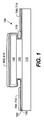
110 基板
120 導電体
130 非導電体
140 レジスト
150 ゲート誘電体
160 半導体
170 凹部形状
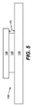
700 電極
710 第2の導電材料層
800 電極
810 第3の導電材料層
Claims (8)
- 基板と、
導電材料層と、
電気絶縁材料層と、
を有し、
前記基板、前記導電材料層及び前記電気絶縁材料層のうちの1つ以上の少なくとも一部が凹部形状を画成している、
トランジスタ。 - 前記電気絶縁材料層は第1の電気絶縁材料層であり、当該トランジスタは更に、前記凹部形状に共形の第2の電気絶縁材料層を有する、請求項1に記載のトランジスタ。
- 前記凹部形状に共形であって前記第2の電気絶縁材料層と接触する半導体材料層、を更に有する請求項2に記載のトランジスタ。
- 前記凹部形状に共形の半導体材料層、を更に有する請求項1に記載のトランジスタ。
- 前記半導体材料層と接触する導電材料層、を更に有する請求項4に記載のトランジスタ。
- 前記基板はフレキシブル基板である、請求項1に記載のトランジスタ。
- 前記電気絶縁材料層と前記導電材料層とが前記凹部形状を画成している、請求項1に記載のトランジスタ。
- 半導体デバイスを作動させる方法であって:
トランジスタを配設し、該トランジスタは:
基板と、
第1の導電材料層と、
電気絶縁材料層であり、該電気絶縁材料層が、前記導電材料層に対して凹部形状を含む、電気絶縁材料層と、
前記電気絶縁材料層上に配置された第2の導電材料層と、
前記基板上に配置された第3の導電材料層と、
を含み;
前記第2の導電材料層と前記第3の導電材料層との間に電圧を印加し;且つ
前記第2の導電材料層と前記第3の導電材料層とを電気的に接続するように前記第1の導電材料層に電圧を印加する;
ことを有する方法。
Applications Claiming Priority (3)
| Application Number | Priority Date | Filing Date | Title |
|---|---|---|---|
| US12/713,264 | 2010-02-26 | ||
| US12/713,264 US8803203B2 (en) | 2010-02-26 | 2010-02-26 | Transistor including reentrant profile |
| PCT/US2011/024310 WO2011106165A1 (en) | 2010-02-26 | 2011-02-10 | Vertical transistor including reentrant profile |
Publications (2)
| Publication Number | Publication Date |
|---|---|
| JP2013520839A true JP2013520839A (ja) | 2013-06-06 |
| JP2013520839A5 JP2013520839A5 (ja) | 2014-02-06 |
Family
ID=43875263
Family Applications (1)
| Application Number | Title | Priority Date | Filing Date |
|---|---|---|---|
| JP2012555025A Pending JP2013520839A (ja) | 2010-02-26 | 2011-02-10 | 内側にへこんだ形状を含んだ縦型トランジスタ |
Country Status (7)
| Country | Link |
|---|---|
| US (2) | US8803203B2 (ja) |
| EP (1) | EP2539924B1 (ja) |
| JP (1) | JP2013520839A (ja) |
| KR (1) | KR20120114372A (ja) |
| CN (1) | CN102782821B (ja) |
| BR (1) | BR112012019907A2 (ja) |
| WO (1) | WO2011106165A1 (ja) |
Cited By (1)
| Publication number | Priority date | Publication date | Assignee | Title |
|---|---|---|---|---|
| JP2016001722A (ja) * | 2014-04-08 | 2016-01-07 | 株式会社半導体エネルギー研究所 | 半導体装置及び該半導体装置を含む電子機器 |
Families Citing this family (9)
| Publication number | Priority date | Publication date | Assignee | Title |
|---|---|---|---|---|
| WO2012094357A2 (en) * | 2011-01-07 | 2012-07-12 | Eastman Kodak Company | Transistor including multiple reentrant profiles |
| US8492769B2 (en) * | 2011-01-07 | 2013-07-23 | Eastman Kodak Company | Transistor including multi-layer reentrant profile |
| US8962988B2 (en) | 2011-02-03 | 2015-02-24 | Solar Junction Corporation | Integrated semiconductor solar cell package |
| US8273654B1 (en) * | 2011-09-29 | 2012-09-25 | Eastman Kodak Company | Producing a vertical transistor including reentrant profile |
| US9006736B2 (en) * | 2013-07-12 | 2015-04-14 | Semiconductor Energy Laboratory Co., Ltd. | Semiconductor device |
| US9147770B1 (en) * | 2014-03-06 | 2015-09-29 | Eastman Kodak Company | VTFT with extended electrode |
| US9123815B1 (en) * | 2014-03-06 | 2015-09-01 | Eastman Kodak Company | VTFTs including offset electrodes |
| US9117914B1 (en) * | 2014-03-06 | 2015-08-25 | Eastman Kodak Company | VTFT with polymer core |
| US9691997B2 (en) * | 2014-06-11 | 2017-06-27 | Eastman Kodak Company | Devices having dielectric layers with thiosulfate-containing polymers |
Citations (3)
| Publication number | Priority date | Publication date | Assignee | Title |
|---|---|---|---|---|
| JPH02140863U (ja) * | 1989-04-26 | 1990-11-26 | ||
| JPH08153878A (ja) * | 1994-11-29 | 1996-06-11 | Sony Corp | 薄膜トランジスタ及びその製造方法 |
| JP2008091379A (ja) * | 2006-09-29 | 2008-04-17 | Sanyo Electric Co Ltd | 電界効果トランジスタ及びその製造方法 |
Family Cites Families (35)
| Publication number | Priority date | Publication date | Assignee | Title |
|---|---|---|---|---|
| JPS63170971A (ja) | 1987-01-09 | 1988-07-14 | Nec Corp | 半導体装置 |
| DE3855889T2 (de) | 1987-12-02 | 1997-08-07 | Advanced Micro Devices Inc | Ein verfahren zur herstellung selbstausrichtender halbleiteranordnungen |
| JPH02140863A (ja) | 1988-11-22 | 1990-05-30 | Nec Corp | 分散型エディタにおける端末側エディタのテキスト送信方式 |
| JPH05144744A (ja) | 1991-11-18 | 1993-06-11 | Nippon Telegr & Teleph Corp <Ntt> | 半導体薄膜形成方法 |
| KR970007965B1 (en) | 1994-05-12 | 1997-05-19 | Lg Semicon Co Ltd | Structure and fabrication method of tft |
| KR0132490B1 (ko) * | 1994-07-21 | 1998-04-16 | 문정환 | 박막트랜지스터 제조방법 |
| US5641694A (en) * | 1994-12-22 | 1997-06-24 | International Business Machines Corporation | Method of fabricating vertical epitaxial SOI transistor |
| KR0165398B1 (ko) * | 1995-05-26 | 1998-12-15 | 윤종용 | 버티칼 트랜지스터의 제조방법 |
| US5780911A (en) * | 1995-11-29 | 1998-07-14 | Lg Semicon Co., Ltd. | Thin film transistor and method for fabricating the same |
| GB0024294D0 (en) * | 2000-10-04 | 2000-11-15 | Univ Cambridge Tech | Solid state embossing of polymer devices |
| DE10234735A1 (de) * | 2002-07-30 | 2004-02-12 | Infineon Technologies Ag | Verfahren zum vertikalen Strukturieren von Substraten in der Halbleiterprozesstechnik mittels inkonformer Abscheidung |
| US6924517B2 (en) * | 2003-08-26 | 2005-08-02 | International Business Machines Corporation | Thin channel FET with recessed source/drains and extensions |
| FR2861501B1 (fr) * | 2003-10-22 | 2006-01-13 | Commissariat Energie Atomique | Dispositif microelectronique a effet de champ apte a former un ou plusiseurs canaux de transistors |
| JP3983222B2 (ja) | 2004-01-13 | 2007-09-26 | Necエレクトロニクス株式会社 | 半導体装置及びその製造方法 |
| US7629633B2 (en) * | 2004-05-20 | 2009-12-08 | Isaac Wing Tak Chan | Vertical thin film transistor with short-channel effect suppression |
| US6972461B1 (en) * | 2004-06-30 | 2005-12-06 | International Business Machines Corporation | Channel MOSFET with strained silicon channel on strained SiGe |
| CN100490180C (zh) * | 2004-10-04 | 2009-05-20 | 松下电器产业株式会社 | 纵向场效应晶体管及其制造方法 |
| JP2006269599A (ja) * | 2005-03-23 | 2006-10-05 | Sony Corp | パターン形成方法、有機電界効果型トランジスタの製造方法、及び、フレキシブルプリント回路板の製造方法 |
| TWI278068B (en) * | 2005-11-03 | 2007-04-01 | Nanya Technology Corp | Growth controlled vertical transistor |
| US7456429B2 (en) * | 2006-03-29 | 2008-11-25 | Eastman Kodak Company | Apparatus for atomic layer deposition |
| US7413982B2 (en) * | 2006-03-29 | 2008-08-19 | Eastman Kodak Company | Process for atomic layer deposition |
| JP2007284766A (ja) | 2006-04-19 | 2007-11-01 | Shimadzu Corp | 縦型プラズマcvd装置 |
| US7410856B2 (en) * | 2006-09-14 | 2008-08-12 | Micron Technology, Inc. | Methods of forming vertical transistors |
| JP2008103636A (ja) | 2006-10-20 | 2008-05-01 | Sumitomo Electric Ind Ltd | 縦型トランジスタ、および縦型トランジスタを作製する方法 |
| JP2008160004A (ja) * | 2006-12-26 | 2008-07-10 | Toshiba Corp | 半導体記憶装置及びその製造方法 |
| US11136667B2 (en) * | 2007-01-08 | 2021-10-05 | Eastman Kodak Company | Deposition system and method using a delivery head separated from a substrate by gas pressure |
| US7789961B2 (en) * | 2007-01-08 | 2010-09-07 | Eastman Kodak Company | Delivery device comprising gas diffuser for thin film deposition |
| JP2008277375A (ja) | 2007-04-26 | 2008-11-13 | Sanyo Electric Co Ltd | 電界効果トランジスタ及びその製造方法 |
| US20090001470A1 (en) * | 2007-06-26 | 2009-01-01 | Anderson Brent A | Method for forming acute-angle spacer for non-orthogonal finfet and the resulting structure |
| KR100889607B1 (ko) | 2007-08-13 | 2009-03-20 | 성균관대학교산학협력단 | 더미 드레인층을 이용한 수직 실린더형 트랜지스터의제조방법 및 이에 의해 제조된 수직 실린더형 트랜지스터 |
| KR100896631B1 (ko) | 2007-08-13 | 2009-05-08 | 성균관대학교산학협력단 | 수직 실린더형 트랜지스터의 제조방법 및 이에 의해 제조된수직 실린더형 트랜지스터 |
| JP2009130165A (ja) * | 2007-11-26 | 2009-06-11 | Sanyo Electric Co Ltd | Cmos半導体装置 |
| KR100960928B1 (ko) * | 2008-01-02 | 2010-06-07 | 주식회사 하이닉스반도체 | 수직형 트랜지스터 및 그의 형성방법 |
| JP2010040580A (ja) | 2008-07-31 | 2010-02-18 | Sanyo Electric Co Ltd | 有機薄膜デバイスの製造方法及び有機薄膜デバイス |
| US8637355B2 (en) * | 2011-08-26 | 2014-01-28 | Eastman Kodak Company | Actuating transistor including single layer reentrant profile |
-
2010
- 2010-02-26 US US12/713,264 patent/US8803203B2/en active Active
-
2011
- 2011-02-10 BR BR112012019907A patent/BR112012019907A2/pt not_active IP Right Cessation
- 2011-02-10 CN CN201180010647.7A patent/CN102782821B/zh not_active Expired - Fee Related
- 2011-02-10 WO PCT/US2011/024310 patent/WO2011106165A1/en active Application Filing
- 2011-02-10 JP JP2012555025A patent/JP2013520839A/ja active Pending
- 2011-02-10 EP EP11704703.5A patent/EP2539924B1/en active Active
- 2011-02-10 KR KR1020127022265A patent/KR20120114372A/ko not_active Application Discontinuation
-
2014
- 2014-05-29 US US14/289,678 patent/US9337828B2/en active Active
Patent Citations (3)
| Publication number | Priority date | Publication date | Assignee | Title |
|---|---|---|---|---|
| JPH02140863U (ja) * | 1989-04-26 | 1990-11-26 | ||
| JPH08153878A (ja) * | 1994-11-29 | 1996-06-11 | Sony Corp | 薄膜トランジスタ及びその製造方法 |
| JP2008091379A (ja) * | 2006-09-29 | 2008-04-17 | Sanyo Electric Co Ltd | 電界効果トランジスタ及びその製造方法 |
Cited By (1)
| Publication number | Priority date | Publication date | Assignee | Title |
|---|---|---|---|---|
| JP2016001722A (ja) * | 2014-04-08 | 2016-01-07 | 株式会社半導体エネルギー研究所 | 半導体装置及び該半導体装置を含む電子機器 |
Also Published As
| Publication number | Publication date |
|---|---|
| US8803203B2 (en) | 2014-08-12 |
| WO2011106165A1 (en) | 2011-09-01 |
| CN102782821A (zh) | 2012-11-14 |
| EP2539924A1 (en) | 2013-01-02 |
| CN102782821B (zh) | 2016-01-13 |
| US20140266402A1 (en) | 2014-09-18 |
| BR112012019907A2 (pt) | 2016-05-10 |
| KR20120114372A (ko) | 2012-10-16 |
| US20110210783A1 (en) | 2011-09-01 |
| US9337828B2 (en) | 2016-05-10 |
| EP2539924B1 (en) | 2019-12-11 |
Similar Documents
| Publication | Publication Date | Title |
|---|---|---|
| JP2013520844A (ja) | 内側にへこんだ形状を含んだトランジスタを製造する方法 | |
| US7985684B1 (en) | Actuating transistor including reduced channel length | |
| US9337828B2 (en) | Transistor including reentrant profile | |
| US8865576B2 (en) | Producing vertical transistor having reduced parasitic capacitance | |
| US8617942B2 (en) | Producing transistor including single layer reentrant profile | |
| US8803227B2 (en) | Vertical transistor having reduced parasitic capacitance | |
| US8409937B2 (en) | Producing transistor including multi-layer reentrant profile | |
| US8623757B2 (en) | Producing a vertical transistor including reentrant profile | |
| US20140377943A1 (en) | Four terminal transistor fabrication | |
| US8674748B2 (en) | Actuating transistor including multi-layer reentrant profile | |
| US8492769B2 (en) | Transistor including multi-layer reentrant profile | |
| US8383469B2 (en) | Producing transistor including reduced channel length | |
| TW201242013A (en) | Transistor including multiple reentrant profiles | |
| US8637355B2 (en) | Actuating transistor including single layer reentrant profile | |
| US20120178246A1 (en) | Producing transistor including multiple reentrant profiles | |
| US8304347B2 (en) | Actuating transistor including multiple reentrant profiles | |
| US8847232B2 (en) | Transistor including reduced channel length | |
| US8847226B2 (en) | Transistor including multiple reentrant profiles | |
| US8592909B2 (en) | Transistor including single layer reentrant profile | |
| WO2012094109A1 (en) | Transistor including reduced channel length |
Legal Events
| Date | Code | Title | Description |
|---|---|---|---|
| A521 | Written amendment |
Free format text: JAPANESE INTERMEDIATE CODE: A523 Effective date: 20131212 |
|
| A621 | Written request for application examination |
Free format text: JAPANESE INTERMEDIATE CODE: A621 Effective date: 20131212 |
|
| A977 | Report on retrieval |
Free format text: JAPANESE INTERMEDIATE CODE: A971007 Effective date: 20141128 |
|
| A131 | Notification of reasons for refusal |
Free format text: JAPANESE INTERMEDIATE CODE: A131 Effective date: 20141202 |
|
| A02 | Decision of refusal |
Free format text: JAPANESE INTERMEDIATE CODE: A02 Effective date: 20150519 |