WO2014136375A1 - 酸化物半導体薄膜トランジスタ用基板 - Google Patents
酸化物半導体薄膜トランジスタ用基板 Download PDFInfo
- Publication number
- WO2014136375A1 WO2014136375A1 PCT/JP2014/000354 JP2014000354W WO2014136375A1 WO 2014136375 A1 WO2014136375 A1 WO 2014136375A1 JP 2014000354 W JP2014000354 W JP 2014000354W WO 2014136375 A1 WO2014136375 A1 WO 2014136375A1
- Authority
- WO
- WIPO (PCT)
- Prior art keywords
- oxide semiconductor
- insulating layer
- protective insulating
- layer
- substrate
- Prior art date
- Legal status (The legal status is an assumption and is not a legal conclusion. Google has not performed a legal analysis and makes no representation as to the accuracy of the status listed.)
- Ceased
Links
Images


Classifications
-
- H—ELECTRICITY
- H10—SEMICONDUCTOR DEVICES; ELECTRIC SOLID-STATE DEVICES NOT OTHERWISE PROVIDED FOR
- H10D—INORGANIC ELECTRIC SEMICONDUCTOR DEVICES
- H10D30/00—Field-effect transistors [FET]
- H10D30/60—Insulated-gate field-effect transistors [IGFET]
- H10D30/67—Thin-film transistors [TFT]
- H10D30/6758—Thin-film transistors [TFT] characterised by the insulating substrates
-
- H—ELECTRICITY
- H10—SEMICONDUCTOR DEVICES; ELECTRIC SOLID-STATE DEVICES NOT OTHERWISE PROVIDED FOR
- H10D—INORGANIC ELECTRIC SEMICONDUCTOR DEVICES
- H10D30/00—Field-effect transistors [FET]
- H10D30/60—Insulated-gate field-effect transistors [IGFET]
- H10D30/67—Thin-film transistors [TFT]
- H10D30/674—Thin-film transistors [TFT] characterised by the active materials
- H10D30/6755—Oxide semiconductors, e.g. zinc oxide, copper aluminium oxide or cadmium stannate
Definitions
- the present invention relates to a substrate used for an oxide semiconductor thin film transistor that can be used in a flexible device such as a display device using liquid crystal or an organic EL element, electronic paper, or an X-ray sensor, a semiconductor device, and a manufacturing method thereof.
- Patent Document 1 a thin film transistor (TFT) using an In—Ga—Zn—O-based oxide semiconductor (InGaZnO) as an active layer can be formed at a relatively low temperature, and a resin substrate can be used. For this reason, it is described that this is a technique suitable for making a flat panel display (FPD) thinner, lighter, and flexible.
- FPD flat panel display
- the threshold voltage of the oxide semiconductor thin film transistor is greatly deviated from 0V. It is disclosed that the problem can be solved by providing a protective layer on the protective layer.
- Patent Document 1 also describes that not only a resin substrate but also a metal substrate such as aluminum whose surface is insulated may be used.
- Patent Document 2 is a patent document relating to a flexible substrate, which has higher heat resistance than a resin substrate by forming an aluminum oxide insulating layer having a porous (porous) structure by anodizing treatment on a metal surface, It is disclosed that a flexible substrate that is excellent in thermal dimensional stability and does not cause a failure such as a short circuit can be obtained.
- Patent Document 3 is a patent document relating to a resin-made flexible substrate, and a gas barrier layer containing a silicon compound is provided on the surface of the resin substrate in order to reduce the permeated gas that permeates the resin substrate.
- a gas barrier layer containing a silicon compound is provided on the surface of the resin substrate in order to reduce the permeated gas that permeates the resin substrate.
- Patent Document 1 describes that a TFT may be manufactured using a metal substrate whose surface is insulated.
- a specific example of the metal substrate and a mode and a specific example of a TFT manufactured using the metal substrate are not described.
- an oxide semiconductor thin film transistor having a configuration described in Patent Document 1 was formed on a metal substrate having a porous aluminum anodized insulating film described in Patent Document 2.
- the manufactured oxide semiconductor thin film transistor does not operate normally. Specifically, the mobility and threshold voltage of the oxide semiconductor thin film transistor did not fall within a predetermined range despite the use of a metal substrate that is expected to have high heat resistance and high gas barrier properties.
- the threshold voltage is slightly minus near zero volts, and is preferably turned off in a state where a slightly negative bias is applied.
- the present invention has been made in view of the above circumstances, a substrate for a flexible oxide semiconductor thin film transistor capable of forming an oxide semiconductor thin film transistor having high mobility and a threshold voltage within a predetermined range, and a substrate for the same.
- a flexible semiconductor device obtained by use is provided.
- the present inventors have adsorbed gas to the porous layer on the surface of the anodized aluminum substrate because the time required for evacuation is long when an aluminum substrate having a porous anodized insulating film is put into a vacuum apparatus. It was speculated that the threshold voltage of the InGaZnO-TFT was greatly changed from 0 V because the adsorbed gas was released during the production or diffused after the production.
- an anodized aluminum substrate provided with a gas barrier layer described in Patent Document 3 was prepared, and an oxide semiconductor thin film transistor was formed thereon to manufacture an oxide semiconductor device.
- a semiconductor device having desired characteristics still cannot be obtained.
- the surface roughness of the anodized aluminum substrate is large, and therefore the gas barrier layer described in Patent Document 3 has one reason that the substrate surface coverage is not sufficient. I understood. Therefore, as a result of further detailed examination of the film configuration of the substrate and the manufacturing method, the above problems have been finally solved and the present invention has been completed.
- a substrate for a flexible oxide semiconductor thin film transistor includes a base material provided with a porous layer formed on at least one surface of a metal base, and the porous layer. And a protective insulating layer containing hydrogen as a main component and containing hydrogen, and the hydrogen concentration in the protective insulating layer is 3.5 ⁇ 10 21 atoms / cm 3 or more and 3.5 ⁇ 10 It is 22 atoms / cm 3 or less, and the thickness of the protective insulating layer is 100 nm or more and 2000 nm or less.
- the silicon compound is preferably at least one selected from silicon nitride, silicon oxide, and silicon oxynitride.
- the porous layer is preferably an anodic oxide film of aluminum or aluminum alloy. Furthermore, the porous layer is preferably formed on both surfaces of the metal base.
- the protective insulating layer is preferably provided at least over the entire region where the active layer formed of an oxide semiconductor is formed.
- the active layer made of an oxide semiconductor preferably contains In, Ga, and Zn.
- the active layer made of an oxide semiconductor is preferably amorphous.
- An oxide semiconductor thin film transistor has at least a gate electrode, a gate insulating film, an active layer made of an oxide semiconductor, a source and a drain electrode.
- the oxide semiconductor thin film transistor is preferably formed over a substrate and includes at least a gate electrode, a gate insulating film, an active layer made of an oxide semiconductor, and a source and drain electrodes in this order. Furthermore, it is preferable that the gate insulating film of the oxide semiconductor thin film transistor has silicon oxide as a main component.
- the method for producing a flexible semiconductor device of the present invention provides a base material having a porous layer on at least one surface on a metal base, and a silicon compound as a main component on at least a part of the porous layer,
- a protective insulating layer having a hydrogen concentration of 3.5 ⁇ 10 21 atoms / cm 3 or more and 3.5 ⁇ 10 22 atoms / cm 3 or less and a thickness of 100 nm or more and 2000 nm or less is formed by plasma CVD (CVD: Chemical Vapor).
- CVD Chemical Vapor
- the substrate having the porous layer before forming the protective insulating layer, it is preferable to heat the substrate having the porous layer under reduced pressure from the atmosphere at 350 ° C. or higher.
- a layer that is provided on the porous layer and mainly contains a silicon compound is referred to as a protective insulating layer.
- main component means that 60% by mass or more of the material constituting the layer is composed of the specified compound.
- an “oxide semiconductor thin film transistor” means a thin film transistor having at least a gate electrode, a gate insulating film, an active layer made of an oxide semiconductor, and source / drain electrodes.
- ... is provided in direct contact with the surface of It shall include both cases where another layer exists and is provided on that layer. Further, in that case,... May be provided in the whole area of ⁇ , or may be provided only in part.
- the substrate for an oxide semiconductor thin film transistor of the present invention includes a porous layer on the surface of the metal base, and further includes a protective insulating layer containing a silicon compound as a main component and containing hydrogen on the porous layer,
- the hydrogen concentration in the protective insulating layer is 3.5 ⁇ 10 21 atoms / cm 3 or more and 3.5 ⁇ 10 22 atoms / cm 3 or less, and the thickness of the protective insulating layer is 100 nm or more and 2000 nm or less.
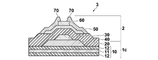
- FIG. 1 is a diagram schematically showing an embodiment of a flexible semiconductor device.
- a flexible oxide semiconductor thin film transistor substrate 1 a includes a base material 10 and a protective insulating layer 20 provided on the base material 10.
- the substrate 10 includes a metal base 11 and a porous layer 12 provided thereon.
- the porous layer 12 is located between the metal base 11 and the protective insulating layer provided thereon, and has a function of improving adhesion of the layer provided thereon by roughening the surface.
- the protective insulating layer 20 prevents the gas adsorbed on the surface of the porous layer 12 from being released into the manufacturing apparatus during the manufacturing process or adversely affecting the oxide semiconductor layer due to diffusion after the manufacturing. Have a role.
- the protective insulating layer 20 also has a role of preventing the base material 10 from being damaged by chemicals such as acid and alkali used, plasma during dry etching and sputtering film formation, and the like during the manufacturing process.
- the protective insulating layer 20 covers the porous layer 12 and has a silicon compound as a main component and a hydrogen concentration of 3.5 ⁇ 10 21 in order to ensure an adsorption gas release prevention function and a manufacturing process damage prevention function.
- a film thickness of atoms / cm 3 or more and 100 nm or more is required. Moreover, in order to ensure the flexibility of the base material 10 and to prevent the protective insulating layer 20 from cracking, the upper limit of the film thickness is 2000 nm.
- the characteristics of the oxide semiconductor thin film transistor are affected by the amount of hydrogen contained in the protective insulating layer 20.
- the protective insulating layer is formed so that the hydrogen concentration is 3.5 ⁇ 10 22 atoms / cm 3 or less.
- the protective insulating layer 20 has a hydrogen concentration set in a range of 3.5 ⁇ 10 21 atoms / cm 3 to 3.5 ⁇ 10 22 atoms / cm 3 and a thickness of 100 nm to 2000 nm.
- the active layer 50 is made of an oxide semiconductor containing at least one element selected from In, Ga, and Zn.
- Patent Document 1 it is known that the threshold voltage of an oxide semiconductor thin film transistor greatly deviates from around 0 V when the active layer is exposed to the atmosphere.
- the base material 10 having the metal base 11 reduces the intrusion of air and water vapor from the outside, the protective insulating layer 20 reduces the gas emission from the porous layer 12, and the protective insulating layer 20 itself also adversely affects the threshold voltage. Therefore, the threshold voltage of the oxide semiconductor thin film transistor is in the vicinity of 0V.
- the substrate the metal base, the porous layer, the protective insulating layer, and the oxide semiconductor thin film transistor will be described in order.
- the substrate 10 includes a metal base 11 and a porous layer 12 formed on at least one surface of the metal base.
- the base material 10 including the metal base 11 and the porous layer 12 is suitable as a flexible substrate for an oxide semiconductor thin film transistor because it has flexibility, gas barrier properties, and process resistance.
- the substrate 10 can be preferably used as long as it has at least the metal base 11 and the porous layer 12, but the metal base 11 is made of a clad material in which aluminum, stainless steel or a steel plate and an aluminum thin plate are integrated. Further, it is more preferable because the anodizing treatment of the aluminum thin plate is simplified and the durability of the base material is increased. Furthermore, in the base material obtained by anodizing the surface of the aluminum thin plate in the clad material in which both surfaces of the steel plate are sandwiched between the aluminum thin plates, the substrate caused by the difference in the thermal expansion coefficient of the material constituting the base material It is more preferable because warpage, film peeling, and the like can be suppressed.
- the substrate 10 provided with the porous layer 12 is preferably subjected to degassing treatment under reduced pressure before forming a protective insulating layer 20 described later.
- degassing treatment By carrying out the degassing treatment, the amount of gas adsorbed on the porous layer can be reduced, which is more preferable.
- a degassing process is performed by heating a substrate provided with a porous layer at 350 ° C. or higher while evacuating the chamber Can be implemented.
- the degassing treatment it is preferable to perform the degassing treatment with a film formation apparatus for forming the protective insulating layer 20 because the protective insulating layer can be provided without being exposed to the atmosphere after the degassing treatment. Further, it is more preferable to perform the treatment in the pretreatment chamber because the possibility that the released gas is taken in again when the protective insulating layer is formed can be reduced.
- This degassing treatment of the porous layer is preferably performed in as short a time as possible in order to avoid deterioration in productivity during mass production.
- the metal base 11 is at least partially made of metal and has a gas barrier property. Further, when a metal base having a thin plate shape is selected, it is preferable because flexibility can be provided while maintaining gas barrier properties.
- Examples of the material of the metal base 11 include aluminum (Al), iron (Fe), zirconium (Zr), titanium (Ti), magnesium (Mg), copper (Cu), niobium (Nb), and tantalum (Ta).
- a substrate containing at least one selected metal or an alloy of the above metals is preferred. Aluminum is preferable from the viewpoint of availability and light weight.
- the metal base 11 may be a single layer or a laminate of a plurality of layers, and the material may be a simple substance or an alloy. For example, for the purpose of adjusting expansion and contraction and warpage due to thermal expansion, it is possible to form a multilayer structure of multiple layers or use an alloy.
- the metal base refers to all portions excluding the porous layer.
- interposed into the porous of both surfaces shall be called a metal base.
- the metal base has a plurality of layers, at least one layer is made of metal.
- FIG. 2 shows an example in which the metal base 11 is composed of a plurality of layers.
- FIG. 2 shows a mode in which the metal base portion 11 has a three-layer configuration, and shows a configuration in which the auxiliary base portion 11a is sandwiched between the main base portions 11b.
- a laminated structure in which the auxiliary base portion 11a and the main base portion 11b are formed one by one is also suitable.
- at least one layer may be a metal, and the other layer may be a metal or not a metal.
- the material used for the metal base may be, for example, a stainless plate or a plate made of carbon fiber.
- the auxiliary base 11a may be employed for the purpose of adjusting the expansion / contraction rate, reinforcing the base material, and reducing the gas permeability.
- a metal thin plate is preferably used, and a stainless steel material is preferably used.
- the total thickness of the metal base 11 (the sum in the case where it is composed of a plurality of layers) can be appropriately selected depending on the application.
- Porous layer 12 is provided on the metal base 11.
- the porous layer 12 is provided on at least a part of the surface of the metal base, and can insulate the surface of the metal base 11 and improve the adhesion of the layer provided thereon by the anchor effect.
- the porous layer 12 is also excellent in the flexibility of the layer itself. From the viewpoint of flexibility, the pore diameter of the porous layer 12 is preferably about 10 nm.
- the porous layer 12 is preferably provided on one entire surface of the metal base, and more preferably on the entire both surfaces of the metal base. When a porous layer is provided equally on both surfaces of the metal base, it is more preferable that the stress becomes uniform and the substrate is less likely to warp.
- FIG. 1 and 2 show a mode in which the metal base 11 and the porous layer 12 are in direct contact with each other, but another layer may be provided between them as necessary.
- an insulating layer for further improving the insulating property of the metal base surface or an underlayer for easily attaching a porous layer may be provided.
- the material of the porous layer 12 is preferably an insulating metal oxide, and more preferably an oxide containing the same metal as the metal base 11.
- the porous layer 12 may be made by any manufacturing method, and a porous layer may be formed by applying a liquid in which insulating porous fine particles and a binder are dispersed to the surface of the metal base 11. May be formed into a porous layer.
- a mode in which a part of the metal base portion is anodized to form a porous layer is preferable.
- the thickness of the porous layer 12 can be appropriately selected depending on the application, but is preferably 0.1 ⁇ m to 100 ⁇ m, more preferably 0.5 ⁇ m to 50 ⁇ m, and more preferably 5 ⁇ m to 20 ⁇ m from the viewpoint of insulation and adhesion. Is most preferred.
- a layer made of a metal oxide is provided as the porous layer 12, it is preferable that the thickness is 50 ⁇ m or less because flexibility is easily secured. Further, it is preferable to set the thickness to 0.5 ⁇ m or more because insulation is easily secured.
- the method for forming the porous layer by the anodizing treatment is not particularly limited, and any method can be used as long as the anodized porous layer can be formed on the metal surface. Below, the porous layer formed by anodic oxidation is demonstrated.
- a method for producing a porous layer using anodization has been known as a simple method capable of forming nanometer-order pores.
- this porous layer is a metal oxide, it is known to have high insulation. Specifically, when a metal substrate is immersed in an acidic or alkaline electrolyte such as sulfuric acid, oxalic acid, or phosphoric acid, and this is used as an anode, oxidation and dissolution occur on the surface of the metal substrate. Simultaneously, an oxide film having pores on its surface can be formed.
- the metal for forming the porous layer using anodization can be selected as appropriate.
- At least one metal selected from copper (Cu), niobium (Nb) and tantalum (Ta), or an alloy of the above metals is preferable.
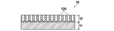
- FIG. 4 shows a schematic diagram of a porous layer obtained by anodizing treatment.
- FIG. 4 shows an embodiment in which a porous layer 12 is provided by anodizing only one side of the metal base 11.
- the surface to be treated of the metal base 11 is uniformly changed to a metal oxide, and nanometer-order pores 120 are formed. Since the surface to be treated is uniformly treated by the anodizing treatment, high insulation can be ensured.
- the porous layer is formed by treating the surface of the original metal base, the metal base 11 and the porous layer 12 are strongly bonded and do not easily peel off.
- the next layer (not shown) is formed on the porous layer, the components of the next layer enter the pores 120 at the time of film formation, so that adhesion is secured by a so-called anchor effect.
- the metal base made of the prepared metal or alloy is washed with water, it is degreased with a metal degreasing agent to remove dirt adhering to the surface, and the degreasing agent is washed away with water washing.
- the nitric acid is washed with a 5% by mass to 20% by mass nitric acid aqueous solution, and then washed again with water.
- the metal base is anodized at a predetermined current density in a sulfuric acid bath or an oxalic acid bath to form a porous anodized film on the surface of the metal base.
- the optimum value of the current flowing during the anodic oxidation process varies depending on the metal species. However, if the current value is too small, the dissolution of the metal becomes dominant and the required porous layer may not be formed. Further, if the current value is too large, the porous layer grows rapidly, so that there is a possibility that the surface is not uniform or a part of the porous layer is easily peeled off.
- a protective insulating layer 20 is provided on at least a part of the surface of the porous layer 12.
- the protective insulating film 20 prevents the gas adsorbed on the surface of the porous layer 12 from being released into the manufacturing apparatus during the manufacturing process or adversely affecting the oxide semiconductor layer due to diffusion after the manufacturing. Have a role.
- the protective insulating layer 20 also has a role of preventing the substrate 10 from being damaged by chemicals such as acids and alkalis used in the manufacturing process, plasma during dry etching and sputtering film formation, and the like.
- FIG. 3 shows a schematic cross-sectional view of a mode in which the protective insulating layer 20 is provided on a part of the porous layer 12.
- the protective insulating layer 20 is preferably provided at least in a region where the active layer 50 of the oxide semiconductor thin film transistor 2 is formed. Moreover, it is more preferable to provide at least the formation region of the oxide semiconductor thin film transistor 2, and it is even more preferable to provide the entire porous layer. Covering only part of the surface of the porous layer with the protective insulating layer can also provide the effect of the invention, but covering the entire surface of the porous layer causes gas to be released from the porous layer during the manufacturing process.
- damage to the substrate 10 due to exposure to plasma, acid / alkali chemicals, and organic solvents during the process of manufacturing the oxide semiconductor thin film transistor is more preferable because the protective insulating layer reduces the damage.
- the protective insulating layer 20 and the base material 10 are described so as to be in direct contact with each other, but another layer may be provided therebetween.
- a planarization layer for reducing unevenness of the porous layer or a base layer for improving adhesion between the porous layer and the protective insulating layer may be provided.
- the protective insulating layer 20 is a layer mainly containing a silicon compound and containing hydrogen.
- any silicon compound may be used as the silicon compound, silicon oxide, silicon nitride, silicon oxynitride, and the like can be prevented in that the base material 10 can be prevented from being damaged during the manufacturing process of the oxide semiconductor thin film transistor 2. It is preferable to do this.
- Such silicon compounds are known to incorporate hydrogen into the film when formed by sputtering or CVD.
- the protective insulating layer is protected by having a silicon compound as a main component, a hydrogen concentration of 3.5 ⁇ 10 21 atoms / cm 3 or more, and a film thickness of 100 nm or more. It was found to function as an insulating layer.
- the function as the protective insulating layer is as follows: (1) Gas adsorbed on the surface of the porous layer 12 is released into the manufacturing apparatus during the manufacturing process, or adversely affects the oxide semiconductor layer by diffusion after manufacturing. (2) The protective insulating layer 20 is damaged during the manufacturing process due to chemicals such as acids and alkalis used in the manufacturing process, plasma during dry etching and sputter deposition, and the like. Three functions: (3) flexibility.
- the base material 10 has a porous layer, and therefore the surface irregularities are severe.
- a protective insulating layer it is necessary to cover a porous layer.
- the hydrogen concentration of the protective insulating layer is less than 3.5 ⁇ 10 21 atoms / cm 3 , the film becomes dense and hard.
- cracks are generated and coverage is poor, it is difficult to satisfactorily coat the porous layer. It was also clarified that even when the hydrogen concentration is 3.5 ⁇ 10 21 atoms / cm 3 or more, a film thickness of 100 nm is required to cover the porous layer with a rough surface.
- the applicants diffuse hydrogen contained in the protective insulating layer and enter the active layer of the oxide semiconductor thin film transistor to increase the amount of carriers in the active layer, thereby increasing the mobility and threshold voltage of the oxide semiconductor thin film transistor. Elucidated the effect. As a result of examining the protective insulating layer in detail, it was found that the threshold voltage of the oxide semiconductor thin film transistor can be controlled within a predetermined range by setting the hydrogen concentration of the protective insulating layer to 3.5 ⁇ 10 22 atoms / cm 3 or less.
- the hydrogen concentration of the protective insulating layer provided on the substrate 10 should be 3.5 ⁇ 10 21 atoms / cm 3 or more and 3.5 ⁇ 10 22 atoms / cm 3 or less.
- atoms / cm 3 means the number of atoms contained per 1 cm 3 .
- the protective insulating layer 20 is provided so as to have the above hydrogen concentration range and film thickness, if the film thickness is too thick, the protective insulating layer 20 cracks when the semiconductor device 3 is bent. As a result, the protective insulating layer 20 may be peeled off, and gas may enter to deteriorate characteristics such as mobility degradation of the oxide semiconductor thin film transistor 2. As a result of investigations by the present inventors, it has been found that, in addition to adjusting the hydrogen concentration, a protective insulating layer having a thickness of 100 nm to 2000 nm is important for solving the problem.
- the protective insulating layer is a layer containing a silicon compound as a main component, and may be a single layer or a plurality of layers of silicon compounds.
- the total film thickness of the plurality of layers is set in a range of 100 nm to 2000 nm.
- the hydrogen concentration of the protective insulating layer closest to the side where the oxide semiconductor thin film transistor is provided is at least 3.5 ⁇ 10 21 atoms / cm 3 among the plurality of protective insulating layers. 5 ⁇ 10 22 atoms / cm 3 or less.
- SIMS Secondary Ion Mass Spectroscopy
- the hydrogen concentration of the protective insulating layer can be measured by a measuring method called dynamic SIMS (D-SIMS: Dynamic-SIMS).
- D-SIMS dynamic SIMS
- the measurement result is obtained as a profile in the depth direction of the constituent element, and the absolute value of the element concentration can be obtained by referring to the profile of the measurement result of the standard substrate whose element content is known in advance.
- cesium ions are used as the primary ions to be collided. Further, since the detection sensitivity is very high, measurement is carried out under ultra-high vacuum (1.0 ⁇ 10- 5 Pa or less).
- the protective insulating layer 20 may be formed by any method, but it is easy to adjust the hydrogen concentration to a range of 3.5 ⁇ 10 21 atoms / cm 3 or more and 3.5 ⁇ 10 22 atoms / cm 3 or less, and 500 ° C. It is preferable that the following low-quality insulating film is formed by plasma CVD (also known as PE-CVD, Plasma Enhanced-CVD) from the viewpoint that a relatively high film formation rate can be realized.
- plasma CVD a reactive gas is brought into a plasma state to generate active radicals and ions, and a chemical reaction is performed in an active environment to form a desired film on an adherend.
- capacitively coupled plasma CVD CCP-CVD
- the hydrogen concentration of the protective insulating layer 20 can be adjusted by the flow rate of the source gas introduced during film formation, the temperature of the substrate on which the protective insulating layer is formed, and the annealing temperature after film formation.
- SiH 4 , NH 3, and H 2 gas are used as the source gas.
- the hydrogen concentration in the protective insulating layer can be adjusted.
- the hydrogen concentration may be adjusted by using a plurality of adjustment methods described above. From the viewpoint of hydrogen concentration reproducibility, hydrogen concentration adjustment by substrate temperature and hydrogen concentration adjustment by H 2 gas flow rate are preferable.
- the protective insulating layer is electrically insulating. Electrical insulation means that the sheet resistance value of the protective insulating layer is 1.0 ⁇ 10 7 ⁇ / ⁇ or more. 1.0 ⁇ 10 9 ⁇ / ⁇ or more is more preferable. The sheet resistance value is preferable because it does not cause a leak or a short circuit between elements of the oxide semiconductor thin film transistor.
- FIG. 1 illustrates a mode in which the oxide semiconductor thin film transistor 2 is provided directly on the protective insulating layer 20, another layer may be provided between the protective insulating layer 20 and the oxide semiconductor thin film transistor 2.
- a planarization film that improves the flatness of the substrate, an insulating layer that further improves insulation, or a base layer that improves adhesion between the oxide semiconductor thin film transistor 2 and the protective insulating layer may be provided.
- a semiconductor device refers to a device including an oxide semiconductor thin film transistor including at least a gate electrode, a gate insulating film, an active layer made of an oxide semiconductor, and source / drain electrodes on a substrate.
- An oxide semiconductor thin film transistor is easy to form on a flexible substrate because of its low film formation temperature, and is a technology that contributes to thinning, lightening, and flexibility of a display device using the oxide semiconductor thin film transistor.
- a device using such an oxide semiconductor generates carriers in the oxide semiconductor when a small amount of impurities are mixed from the outside, so that the base material is thinner than a conventional thin film transistor using silicon as an active layer.
- the impurity content of the adjacent layer is important.
- FIG. 1 includes a gate electrode 30, a gate insulating film 40, an active layer 50, an etching stopper layer 60, and a source / drain electrode 70.
- a bottom gate type oxide semiconductor thin film transistor is described in FIG. 1, a top gate type or a type having a plurality of gate electrodes are within the scope of the present invention.
- the etching stopper layer 60 is shown in FIG. 1, a configuration in which the etching stopper layer 60 is not provided when not particularly necessary is also within the scope of the present invention. Further, other configurations can be changed within the scope of the present invention.
- each part (active layer, etching stopper layer, gate electrode, gate insulating film, source / drain electrode) constituting the oxide semiconductor thin film transistor will be described with reference to FIG.
- the active layer 50 is made of an oxide semiconductor.
- Oxide semiconductors have a relatively low deposition temperature and high mobility even without a high-temperature crystallization step.
- an oxide semiconductor containing at least one element selected from In, Ga, and Zn is used as a material for the active layer 50.
- an oxide semiconductor (InGaZnO) containing In, Ga, and Zn is preferable because high mobility can be obtained.
- an oxide semiconductor carriers are generated by mixing hydrogen without depending on the composition thereof, which causes a problem that the threshold voltage deviates greatly from the vicinity of 0V. Therefore, the effects of the invention can be exhibited in an apparatus including an oxide semiconductor thin film transistor that employs a substrate having a metal base and a porous layer and uses an oxide semiconductor as an active layer.
- the active layer 50 functions as a layer that generates carriers when a voltage is applied to the gate electrode 30.
- the oxide semiconductor constituting the active layer 50 include In 2 O 3 , ZnO, Indium-Zinc-Oxide (InZnO), Gallium-Zinc-Oxide (GaZnO), Indium-Gallium-Oxide (InGaO), and Indium— Gallium-Zinc-Oxide (InGaZnO) is used.
- InGaZnO is preferable in that high mobility and low off-state current can be obtained.
- the active layer 50 is preferably composed of an amorphous oxide semiconductor that can be formed over a substrate having low heat resistance among oxide semiconductors.
- a crystalline oxide semiconductor can be selected.
- an amorphous oxide semiconductor containing at least In, Ga, or Zn is preferable.
- the amorphous oxide semiconductor used for the active layer 50 is configured as an oxide containing In, Ga, and Zn, and is amorphous with a composition in a crystalline state represented by InGaO 3 (ZnO) m (m is a natural number of 5 or less).
- An oxide semiconductor is preferable, and an amorphous oxide semiconductor represented by InGaZnO 4 is particularly preferable.
- an amorphous oxide semiconductor having this composition the electron mobility tends to increase as the electrical conductivity increases.
- the electric conductivity can be controlled by adjusting the oxygen partial pressure during film formation. Whether or not the oxide semiconductor is amorphous can be confirmed by X-ray diffraction measurement. When X-ray diffraction measurement is performed and no diffraction peak is observed, the film is amorphous.
- the active layer 50 preferably has a thickness of 1 nm to 200 nm, more preferably 2.5 nm to 100 nm.
- the method for manufacturing the active layer 50 is not particularly limited. For example, it is formed using a wet method such as a printing method or a coating method, a physical method such as a vacuum deposition method, a sputtering method, or an ion plating method, or a chemical method such as CVD or plasma CVD method.
- a forming method is appropriately selected in consideration of suitability with the material constituting the active layer 50.
- an oxide semiconductor containing In, Ga, and Zn is used as the active layer, it is preferably formed by a sputtering method from the viewpoint that a high-quality film can be formed even at a low temperature.
- oxide semiconductors particularly oxide semiconductor thin film transistors using an amorphous oxide semiconductor as an active layer
- oxide semiconductor thin film transistors using an amorphous oxide semiconductor as an active layer can obtain high mobility even when manufactured on a substrate with a rough surface. Therefore, it is suitable as a thin film transistor provided over the substrate of the present invention.
- a thin film transistor using Si as an active layer and a thin film transistor using an organic semiconductor as an active layer are sensitive to the surface shape of the substrate, and desired characteristics cannot be obtained unless the substrate surface is flat. Therefore, it is not suitable as a transistor provided over the substrate of the present invention having relatively large surface irregularities.
- the etching stopper layer 60 functions as an etching stopper that protects the active layer 50, particularly the channel region C, from being etched when the source / drain electrodes 70 are patterned.
- the etching stopper layer also serves to prevent impurities from entering the active layer from the outside.
- This etching stopper layer 60 is preferably provided so as to cover at least the channel region C of the active layer 50.
- the etching stopper layer is preferably made of silicon or gallium oxide. For example, silicon oxide, gallium oxide, silicon nitride, silicon oxynitride, and titanium oxide are preferably used.
- the etching stopper layer 60 preferably has a thickness of 10 nm to 300 nm, more preferably 50 nm to 150 nm.
- the manufacturing method of the etching stopper layer 60 is not particularly limited, but is a wet method such as a printing method and a coating method, a physical method such as a vacuum deposition method, a sputtering method, and an ion plating method, CVD, plasma CVD. It is formed using a chemical method such as a method. Among these, a forming method is appropriately selected in consideration of suitability with the material constituting the etching stopper layer 60. For example, when silicon oxide is used as the etching stopper layer 60, a plasma CVD method is preferably used.
- the gate electrode 30 is made of, for example, a metal such as Al, Mo, Cr, Ta, Ti, Au, or Ag, or an alloy thereof, an alloy such as Al—Nd, APC, tin oxide, zinc oxide, indium oxide, or indium tin oxide. It is formed using a metal oxide conductive material such as (ITO) or indium zinc oxide (InZnO), an organic conductive compound such as polyaniline, polythiophene, or polypyrrole, or a mixture thereof. As the gate electrode 30, it is preferable to use Mo, an Mo alloy (Mo-5 at% Nb or the like) or Cr.
- the thickness of the gate electrode 30 is, for example, 10 nm to 1000 nm. Further, it is more preferably 20 nm to 500 nm, and further preferably 40 nm to 100 nm.
- the formation method of the gate electrode 30 is not particularly limited. For example, it is formed using a wet method such as a printing method or a coating method, a physical method such as a vacuum deposition method, a sputtering method, or an ion plating method, or a chemical method such as CVD or plasma CVD method. Among these, a formation method is appropriately selected in consideration of suitability with the material constituting the gate electrode 30. For example, when the gate electrode 30 is formed using Mo or Mo alloy, it is preferable to use a DC sputtering method.
- the gate insulating film 40 includes an insulator such as SiO 2 , SiN x , SiON, Al 2 O 3 , Y s O 3 , Ta 2 O 5 , or HfO 2 , or a mixed crystal compound containing at least two of these compounds. Is used.
- SiO 2 is most preferably used from the viewpoint of insulation. In the oxide semiconductor thin film transistor, it is preferable to use SiO 2 for the gate insulating film because an excellent semiconductor device having both high mobility and low off-state current can be realized.
- the thickness of the gate insulating film 40 is preferably 10 nm to 10 ⁇ m.
- the gate insulating film 40 needs to be thick to some extent in order to reduce leakage current and increase voltage resistance.
- the thickness of the gate insulating film 40 is more preferably 50 nm to 1000 nm. More preferably, it is 100 nm to 500 nm.
- a high dielectric constant insulator such as HfO 2 can be used for the gate insulating film 40.
- the oxide semiconductor thin film transistor can be driven at a low voltage.
- the formation method of the gate insulating film 40 is not particularly limited. For example, it is formed using a wet method such as a printing method or a coating method, a physical method such as a vacuum deposition method, a sputtering method, or an ion plating method, or a chemical method such as CVD or plasma CVD method.
- the source electrode / drain electrode 70 is made of, for example, a metal such as Al, Mo, Cr, Ta, Ti, Au, or Ag, or an alloy thereof, an alloy such as Al—Nd, APC, tin oxide, zinc oxide, indium oxide, It is formed using a metal oxide conductive material such as indium tin oxide (ITO) or indium zinc oxide (InZnO).
- ITO indium tin oxide
- InZnO indium zinc oxide
- the ITO may be amorphous ITO or crystallized ITO.
- the source / drain electrode 70 it is preferable to use Mo or Mo alloy.
- the thickness of the source / drain electrode 70 is, for example, 10 nm to 1000 nm. A particularly preferred range is 50 nm to 400 nm.
- the formation method of the source electrode / drain electrode 70 is not particularly limited.
- the conductive film having the above composition is, for example, a printing method, a wet method such as a coating method, a physical method such as a vacuum deposition method, a sputtering method, or an ion plating method, a chemical method such as CVD or a plasma CVD method, etc. It is formed using.
- the source / drain electrode 70 is formed of Mo, Mo alloy, or amorphous ITO
- a resist pattern is formed on the Mo film, Mo alloy film, or amorphous ITO film using a photolithography method, and an acid etching solution is used. Then, the source electrode / drain electrode 70 is formed by etching the Mo film, the Mo alloy film, or the amorphous ITO film.
- the protective film may be an inorganic film such as silicon oxide or silicon nitride, an organic film such as an acrylic resin or a polyimide resin, or a laminated structure of an inorganic film / organic film.
- a pixel electrode is provided and is electrically connected to a source electrode of the oxide semiconductor thin film transistor.
- the flexible oxide semiconductor thin film transistor substrate of the present invention and the semiconductor device using the substrate have been described based on the preferred embodiments, but the present invention is not limited to the above embodiments.
- the semiconductor device of the present invention can be used for a display device using liquid crystal, an EL element, electronic paper, and an X-ray sensor.
- the display device using the semiconductor device of this embodiment can be applied to a wide range of fields including a mobile phone display, a personal digital assistant (PDA), a computer display, an automobile information display, and a TV monitor.
- PDA personal digital assistant
- the semiconductor device of the present invention will be specifically described based on examples, but the present invention is not limited thereto.
- the base material used by the Example of this invention and a comparative example is demonstrated.
- -Manufacture of substrate A- A method for manufacturing the substrate 10 having the configuration shown in FIG. 1 will be described.
- a commercially available high-purity aluminum (purity 99.99%) was rolled to prepare an aluminum thin plate having a thickness of 40 ⁇ m.
- the end face of this thin plate was covered with a masking film, then ultrasonically cleaned with ethanol, and electropolished with an acetic acid + perchloric acid solution.
- a porous layer (aluminum anodic oxide film) is formed on the surface of aluminum (both surfaces of two layers of aluminum) by constant-voltage electrolysis at 40 V in an 80 g / L oxalic acid aqueous solution. B was obtained.
- the cross-section TEM of the obtained base material B was measured, it was the structure of the base material 10 of FIG.
- the thickness of the auxiliary base portion 11a (made of stainless steel) was 50 ⁇ m
- the thickness of the main base portion 11b (made of aluminum). Both were 20 ⁇ m
- the thickness of the porous layer 12 was about 10 ⁇ m on both sides.
- the average pore size of the porous layer 12 was confirmed from the cross-sectional TEM image, it was about 10 nm.
- Example 1 Degassing treatment of base material and formation of protective insulating layer ⁇
- the base material A was put into the pretreatment chamber of the protective insulating layer deposition apparatus, and the pretreatment chamber was evacuated to 10 Pa or less, and then the base material A was heated to 450 ° C. and subjected to degassing for 30 minutes. .
- the substrate A When the temperature of the substrate A is lowered, the substrate A is moved from the pretreatment chamber to the film formation chamber, and silicon nitride is formed on the porous layer of the substrate A under the conditions described in the following film formation conditions 1-1 in Table 1. A protective insulating layer containing as a main component was formed on both sides. As a result, an oxide semiconductor thin film transistor substrate having the configuration shown in FIG. 1a was obtained (hereinafter, the substrate having this configuration is referred to as substrate A).
- the film formation temperature represents the average temperature of the base material during the formation of the protective insulating layer.
- the annealing temperature indicates the processing temperature when annealing is performed by heating after the protective insulating layer is formed. In this case, the annealing time is constant at 60 minutes.
- a support made of alkali-free glass having a thickness of 0.7 mm is separately prepared, and the substrate A and the alkali-free glass substrate are bonded (not shown) with a heat-foamable adhesive (Riva Alpha 31950E manufactured by Nitto Denko Corporation). A substrate was obtained. In this manner, the flexible substrate can be easily handled by bonding to a highly rigid support, and the influence of warpage and expansion / contraction can be reduced.
- oxide semiconductor thin-film transistor 2 of FIG. 1 the manufacturing method of the oxide semiconductor thin-film transistor 2 of FIG. 1 is demonstrated.
- the substrate A described above was used as the oxide semiconductor thin film transistor substrate 1a in FIG.
- a MoNb (Mo-5 at% Nb) film having a thickness of 50 nm is used on the surface of the substrate A (the surface of the porous layer 20) by DC magnetron sputtering using Ar gas as the sputtering gas at a substrate temperature of room temperature.
- Ar gas as the sputtering gas at a substrate temperature of room temperature.
- a resist film (TSMR-8900LB, manufactured by Tokyo Ohka Kogyo Co., Ltd.) is formed on the MoNb film by spin coating, and a predetermined pattern is exposed and developed by a photolithography method (Developer: Tokyo Ohka Kogyo Co., Ltd., NMD). -W) to form a resist pattern.
- the MoNb film at the opening of the resist film was etched using phosphoric acid-acetic acid water (Hayashi Junyaku Kogyo Co., Ltd., Mo etchant TSL). Thereafter, the resist film was peeled off (stripping solution: manufactured by Tokyo Ohka Kogyo Co., Ltd., stripping solution 104). As a result, the gate electrode 30 made of MoNb was formed on the protective insulating layer of the substrate A as shown in FIG.
- a gate insulating film 40 made of silicon oxide having a thickness of 200 nm was formed using an RF gas sputtering method so as to cover the gate electrode 30 and using Ar gas and O 2 gas as sputtering gases.
- the substrate temperature was set to room temperature
- the flow rate of Ar gas was 30 sccm
- the flow rate of O 2 gas was 4.0 sccm
- the pressure when introducing Ar gas and O 2 gas was 0.16 Pa.
- an active layer 50 made of InGaZnO having a thickness of 50 nm was formed on the gate insulating film 40 by DC sputtering without opening to the atmosphere.
- the active layer was formed using a polycrystalline sintered body having a composition of InGaZnO 4 as a target and using Ar gas and O 2 gas as sputtering gases.
- the flow rate of Ar gas was 97 sccm
- the flow rate of O 2 gas was 4.2 sccm
- the pressure when introducing Ar gas and O 2 gas was 0.37 Pa.
- an active layer was separately formed on a glass substrate, and X-ray diffraction measurement was performed. Since no diffraction peak was observed, it was confirmed that the active layer was amorphous.
- a resist film (TSMR-8900LB, manufactured by Tokyo Ohka Kogyo Co., Ltd.) is formed on the active layer 50 by spin coating, and is exposed and developed into a predetermined pattern by a photolithography method (developer: manufactured by Tokyo Ohka Kogyo Co., Ltd., NMD-W) to form a resist pattern.
- the active layer 50 at the opening of the resist film was etched using oxalic acid water (ITO-06N, manufactured by Kanto Chemical Co., Inc.). Thereafter, the resist film was peeled off (stripping solution: manufactured by Tokyo Ohka Kogyo Co., Ltd., stripping solution 104).
- an active layer 50 made of an InGaZnO film was formed on the gate insulating film 40 as shown in FIG.
- a silicon oxide film having a thickness of 100 nm was formed as an etching stopper layer 60 so as to cover the active layer 50 by RF sputtering using Ar gas and O 2 gas as sputtering gases.
- the substrate temperature was set to room temperature
- the flow rate of Ar gas was 30 sccm
- the flow rate of O 2 gas was 4.0 sccm
- the pressure when introducing Ar gas and O 2 gas was 0.16 Pa.
- a resist film manufactured by Tokyo Ohka Kogyo Co., Ltd., SMR-8900LB
- the resist film was patterned by exposing and developing (developing solution: stripping solution 104 manufactured by Tokyo Ohka Kogyo Co., Ltd.) so that the resist covering the channel region C (see FIG. 1) remains.
- developer solution stripping solution 104 manufactured by Tokyo Ohka Kogyo Co., Ltd.
- the etching stopper layer 60 exposed in the opening of the resist film was etched by dry etching using CHF 3 gas with an RIE (Reactive ion etching) apparatus. After etching, the resist film was peeled off after oxygen ashing using an RIE apparatus (stripping solution: NMD-W, manufactured by Tokyo Ohka Kogyo Co., Ltd.).
- a molybdenum film having a thickness of 200 nm was formed as the source / drain electrode 70 so as to cover the patterned active layer 50 and the etching stopper layer 60.
- the film was formed by DC sputtering using Ar gas as the sputtering gas and the substrate temperature at room temperature.
- a resist film (manufactured by Tokyo Ohka Kogyo Co., Ltd., SMR-8900LB) is formed on the molybdenum film, and a predetermined pattern is exposed and developed by a photolithography method (developer: Tokyo Ohka Kogyo Co., Ltd., NMD-W).
- a photolithography method developer: Tokyo Ohka Kogyo Co., Ltd., NMD-W
- the molybdenum film in the resist opening was etched using phosphorous nitrate acetic acid (Kanto Chemical Co., Ltd., Al etching solution). Thereafter, the resist film was peeled off (stripping solution: manufactured by Tokyo Ohka Kogyo Co., Ltd., stripping solution 104).
- stripping solution manufactured by Tokyo Ohka Kogyo Co., Ltd., stripping solution 104.
- source / drain electrodes 70 made of molybdenum were formed.
- the active layer 50 of the oxide semiconductor thin film transistor 2 manufactured in this example is covered with the etching stopper layer 60 and the source / drain electrodes 70, and has no structure exposed to the outside air. With this configuration, a semiconductor device 3 that is not affected by the outside air environment can be manufactured without forming a protective film over the oxide semiconductor thin film transistor 2.
- the obtained laminate was placed on a hot plate and heated to 200 ° C., whereby the support made of non-alkali glass and the substrate A were peeled off. Further, the substrate A (the oxide semiconductor thin film transistor provided) obtained by peeling was annealed at 250 ° C. for 1 hour.
- the manufactured oxide semiconductor thin film transistor has a channel length of 30 ⁇ m and a channel width of 90 ⁇ m.
- the semiconductor device of Example 1 was obtained by the above method.
- the hydrogen concentration, mobility, threshold voltage, and flexibility of the protective insulating layer of the obtained semiconductor device were measured by the following methods, and the results are shown in Table 3.
- the hydrogen concentration of the protective insulating layer 20 provided on the substrate 10 was measured as follows.
- the obtained oxide semiconductor thin film transistor was put into a D-SIMS apparatus (AMETEK, IMS-6f), the inside of the chamber was evacuated to a high vacuum, and then the primary ion was formed in the region provided with the active layer made of the oxide semiconductor.
- the sample was set so as to be irradiated. While digging a sample by sputtering, mass analysis of secondary ions was performed. Cesium ions were used as primary ions. A profile in the depth direction of the elements composing the sample was obtained. The position of the protective insulating layer was identified from the profile of the constituent elements, and the average amount of hydrogen atoms detected in the entire protective insulating layer was defined as the hydrogen concentration of the protective insulating layer.
- the hydrogen concentration obtained by measuring a standard substrate in which the amount of doped hydrogen is known in advance under exactly the same conditions as the sample is used.
- the hydrogen concentration in the protective insulating layer was calibrated.
- the standard substrate is made of the same material as the protective insulating layer.
- the protective insulating film is mainly composed of silicon nitride (SiN)
- SiN substrate is used as the standard substrate.
- the protective insulating film is mainly composed of silicon oxide (SiO 2 )
- the standard substrate is composed of SiO 2.
- a substrate is used.
- the voltage between the drain and gate electrodes is fixed at 10 V
- the voltage between the gate and source electrodes is manipulated from ⁇ 10 V to 15 V
- the current flowing between the drain and gate electrodes is Measured (FIG. 5).
- the measurement was performed using a semiconductor parameter analyzer 4156C (manufactured by Agilent Technologies) at room temperature in a dark room. Based on this measurement result, the mobility of the oxide semiconductor thin film transistor was calculated. In this measurement region, the oxide semiconductor thin film transistor is in the saturation region, and thus the mobility was calculated using the following equation.
- Mobility ⁇ [2L / (W * Cox)] ⁇ ( ⁇ Id / ⁇ Vg) 1/2 (L: channel length of oxide semiconductor thin film transistor, W: channel width of oxide semiconductor thin film transistor, Cox: capacitance per unit area of gate insulating film, Id: drain-gate current, Vg: gate-source voltage ) Evaluation was given as follows according to the obtained mobility value.
- V on the threshold voltage of the oxide semiconductor thin film transistor
- evaluation was performed based on the following criteria. When the threshold voltage falls within the range of evaluation A, the driving voltage of the thin film transistor can be lowered, and the current when off (for example, the gate voltage is 0 V) can be reduced.
- the obtained oxide semiconductor thin film transistor was continuously bent 10 times so as to have a curvature radius of 100 mm, and then the mobility of the oxide semiconductor thin film transistor was measured. The obtained mobility was compared with the mobility before bending, and evaluation was given as follows.
- Example 2 A semiconductor device in the same manner as in Example 1 except that the base material A in Example 1 was changed to the base material B (the substrate B was degassed and the substrate provided with the protective insulating layer was referred to as the substrate B). Were manufactured and evaluated.
- Example 3 A semiconductor device was manufactured and evaluated in the same manner as in Example 1 except that the film formation condition 1-1 of the protective insulating layer in Example 1 was changed to the film formation condition 1-2.
- Example 4 A semiconductor device was manufactured and evaluated in the same manner as in Example 3 except that the base material A in Example 3 was changed to the base material B.
- Example 5 A semiconductor device was manufactured and evaluated in the same manner as in Example 1 except that the film forming condition 1-1 of the protective insulating layer in Example 1 was changed to the film forming condition 1-3.
- Example 6 A semiconductor device was manufactured and evaluated in the same manner as in Example 5 except that the base material A in Example 5 was changed to the base material B.
- Example 1 The semiconductor is the same as in Example 1 except that the porous layer and the protective insulating layer obtained by replacing the base material A of Example 1 with a glass substrate are not provided, and that the bonding with the support is not performed. A device was manufactured and evaluated.
- Example 1 A semiconductor device was manufactured and evaluated in the same manner as in Example 1 except that the film formation condition 1-1 of the protective insulating layer in Example 1 was changed to the film formation condition 1-S in Table 2 below. It was. Note that in the method of film formation condition 1-S, the annealing treatment after the formation of the protective insulating layer is not performed.
- Example 2 A semiconductor device was manufactured and evaluated in the same manner as in Example 1 except that the film formation condition 1-1 of the protective insulating layer in Example 1 was changed to the film formation condition 1-4 in Table 1.
- Comparative Example 3 A semiconductor device was manufactured and evaluated in the same manner as in Comparative Example 2 except that the base material A in Comparative Example 2 was replaced with the base material B.
- Example 4 A semiconductor device was manufactured and evaluated in the same manner as in Example 1 except that the film formation condition 1-1 of the protective insulating layer in Example 1 was changed to the film formation condition 1-5 in Table 1.
- Comparative Example 5 A semiconductor device was manufactured and evaluated in the same manner as in Comparative Example 4 except that the base material A in Comparative Example 4 was replaced with the base material B.
- Examples 1 to 6 and Comparative Examples 1 to 5 are semiconductor devices manufactured by using silicon nitride as the material for the protective insulating layer and adjusting the hydrogen concentration.
- Reference Example 1 is a semiconductor device using a glass substrate as a substrate. Table 3 shows the main points of the configuration and the evaluation results.
- the semiconductor devices of Examples 1 to 6 of the present invention have high mobility, a threshold voltage of a predetermined value, and excellent flexibility.
- the semiconductor device of Comparative Example 1 since the hydrogen concentration of the protective insulating layer formed by RF sputtering is too low, the protective insulating layer cannot completely cover the porous layer, and gas is generated during the process. Oxide semiconductor thin film transistors did not operate because they were generated or the substrate was damaged. Further, in the semiconductor devices of Comparative Example 2 and Comparative Example 3, although the protective insulating layer was formed by plasma CVD, since the hydrogen concentration of the protective insulating layer was reduced too much, the protective insulating layer was cracked, and the mobility was low. The transistor did not work after the bending test.
- Example 11 A semiconductor device was manufactured and evaluated in the same manner as in Example 1 except that the film formation condition 1-1 of the protective insulating layer in Example 1 was changed to the film formation condition 2-1 in Table 4 below. It was.
- the source gas TEOS means Tetra ethylene silane.
- the film forming temperature represents the temperature of the base material on which the protective insulating layer is being formed. Note that none of the film forming conditions 2-1 to 2-5 is subjected to annealing after the formation of the protective insulating layer.
- Example 12 A semiconductor device was manufactured and evaluated in the same manner as in Example 11 except that the base material A in Example 11 was changed to the base material B.
- Example 13 A semiconductor device was manufactured and evaluated in the same manner as in Example 11 except that the film formation condition 2-1 of the protective insulating layer in Example 11 was changed to the film formation condition 2-2.
- Example 14 A semiconductor device was manufactured and evaluated in the same manner as in Example 13 except that the base material A in Example 13 was changed to the base material B.
- Example 15 A semiconductor device was manufactured and evaluated in the same manner as in Example 11 except that the film formation condition 2-1 of the protective insulating layer in Example 11 was changed to the film formation condition 2-3.
- Example 16 A semiconductor device was manufactured and evaluated in the same manner as in Example 15 except that the base material A in Example 15 was changed to the base material B.
- Example 11 A semiconductor device was manufactured and evaluated in the same manner as in Example 11 except that the film formation condition 2-1 of the protective insulating layer in Example 11 was changed to the film formation condition 2-4.
- Comparative Example 12 A semiconductor device was manufactured and evaluated in the same manner as in Comparative Example 11 except that the base material A in Comparative Example 11 was replaced with the base material B.
- Example 13 A semiconductor device was manufactured and evaluated in the same manner as in Example 11 except that the film formation condition 2-1 of the protective insulating layer in Example 11 was changed to the film formation condition 2-5.
- Comparative Example 14 A semiconductor device was manufactured and evaluated in the same manner as in Comparative Example 13 except that the base material A in Comparative Example 13 was replaced with the base material B.
- Examples 11 to 16 and Comparative Examples 11 to 14 are semiconductor devices manufactured by using silicon oxide as a material for the protective insulating layer and adjusting the hydrogen concentration.
- Table 5 shows the main points of the configuration and the evaluation results.
- the semiconductor devices of Examples 11 to 16 of the present invention have high mobility, a threshold voltage in the vicinity of 0 V, and excellent flexibility.
- the protective insulating layer was formed by plasma CVD, the protective insulating layer was cracked by bending because the hydrogen concentration of the protective insulating layer was excessively lowered. The mobility after the test changed greatly.
- the threshold voltage deviated greatly from the vicinity of 0 V due to the adverse effect of hydrogen. From the results shown in Tables 4 and 5, it can be seen that the hydrogen concentration range that can solve the problem does not change even if the material of the protective insulating layer changes.
- Example 21 A semiconductor device was manufactured and evaluated in the same manner as in Example 1 except that the protective insulating layer thickness in Example 1 was changed from 400 nm to 100 nm.
- Example 22 A semiconductor device was manufactured and evaluated in the same manner as in Example 21 except that the base material A in Example 21 was changed to the base material B.
- Example 23 A semiconductor device was manufactured and evaluated in the same manner as in Example 1 except that the thickness of the protective insulating layer in Example 1 was changed from 400 nm to 2000 nm.
- Example 24 A semiconductor device was manufactured and evaluated in the same manner as in Example 23 except that the base material A in Example 23 was changed to the base material B.
- Example 25 A semiconductor device was manufactured and evaluated in the same manner as in Example 3 except that the thickness of the protective insulating layer in Example 3 was changed from 400 nm to 2000 nm.
- Example 26 A semiconductor device was manufactured and evaluated in the same manner as in Example 25 except that the base material A in Example 25 was changed to the base material B.
- Example 21 A semiconductor device was manufactured and evaluated in the same manner as in Example 1 except that the thickness of the protective insulating layer in Example 1 was changed from 400 nm to 80 nm.
- Comparative Example 22 A semiconductor device was manufactured and evaluated in the same manner as in Comparative Example 21 except that the base material A in Comparative Example 21 was changed to the base material B.
- Example 23 A semiconductor device was manufactured and evaluated in the same manner as in Example 1 except that the thickness of the protective insulating layer in Example 1 was changed from 400 nm to 2500 nm.
- Comparative Example 24 A semiconductor device was manufactured and evaluated in the same manner as in Comparative Example 23 except that the base material A in Comparative Example 23 was replaced with the base material B.
- Examples 21 to 26 and Comparative Examples 21 to 24 are semiconductor devices prepared by changing the thickness of the protective insulating layer made of silicon nitride. Table 6 shows the main points of the configuration and the evaluation results.
- the semiconductor devices of Examples 21 to 26 of the present invention have high mobility, a threshold voltage in the vicinity of 0 V, and excellent flexibility.
- the semiconductor devices of Comparative Example 21 and Comparative Example 22 since the protective insulating layer is too thin, the mobility of the oxide semiconductor thin film transistor is low due to the influence of the gas from the porous layer, and the threshold voltage is low. It is out of the predetermined value.
- the oxide semiconductor thin film transistors of Comparative Example 23 and Comparative Example 24 since the protective insulating layer is too thick, the protective insulating layer is cracked by the bending test, and the mobility before and after the bending test changes greatly. Was.
- Example 31 A semiconductor device was manufactured and evaluated in the same manner as in Example 11 except that the thickness of the protective insulating layer in Example 11 was changed from 400 nm to 100 nm.
- Example 32 A semiconductor device was manufactured and evaluated in the same manner as in Example 31 except that the base material A in Example 31 was changed to the base material B.
- Example 33 A semiconductor device was manufactured and evaluated in the same manner as in Example 11 except that the thickness of the protective insulating layer in Example 11 was changed from 400 nm to 2000 nm.
- Example 34 A semiconductor device was manufactured and evaluated in the same manner as in Example 33 except that the base material A in Example 33 was changed to the base material B.
- Example 35 A semiconductor device was manufactured and evaluated in the same manner as in Example 15 except that the thickness of the protective insulating layer in Example 15 was changed from 400 nm to 100 nm.
- Example 36 A semiconductor device was manufactured and evaluated in the same manner as in Example 35 except that the base material A in Example 35 was changed to the base material B.
- Example 37 A semiconductor device was manufactured and evaluated in the same manner as in Example 13 except that the thickness of the protective insulating layer in Example 13 was changed from 400 nm to 2000 nm.
- Example 38 A semiconductor device was manufactured and evaluated in the same manner as in Example 37 except that the base material A in Example 37 was changed to the base material B.
- Example 31 A semiconductor device was manufactured and evaluated in the same manner as in Example 11 except that the thickness of the protective insulating layer in Example 11 was changed from 400 nm to 80 nm.
- Comparative Example 32 A semiconductor device was manufactured and evaluated in the same manner as in Comparative Example 31 except that the base material A in Comparative Example 31 was replaced with the base material B.
- Example 33 A semiconductor device was manufactured and evaluated in the same manner as in Example 11 except that the thickness of the protective insulating layer in Example 11 was changed from 400 nm to 2500 nm.
- Comparative Example 34 A semiconductor device was manufactured and evaluated in the same manner as in Comparative Example 33 except that the base material A in Comparative Example 33 was replaced with the base material B.
- Examples 31 to 38 and Comparative Examples 31 to 34 are semiconductor devices created by changing the thickness of the protective insulating layer made of silicon oxide. Table 7 shows the main points of the configuration and the evaluation results.
- the semiconductor devices of Examples 31 to 38 of the present invention have high mobility, a threshold voltage in the vicinity of 0 V, and excellent flexibility.
- the oxide semiconductor thin film transistor did not operate due to the influence of the gas from the porous layer because the protective insulating layer was too thin.
- the protective insulating layer was too thick, the protective insulating layer was cracked by the bending test, and the mobility before and after the bending test was greatly changed. From the results of Tables 6 and 7, it can be seen that there is no difference in the film thickness range that can solve the problem even if the material of the protective insulating layer changes.
- Example 41 A semiconductor device was manufactured and evaluated in the same manner as in Example 1 except that the active layer of Example 1 was changed from InGaZnO to InZnO.
- Example 42 A semiconductor device was manufactured and evaluated in the same manner as in Example 41 except that the base material A in Example 41 was changed to the base material B.
- Example 43 A semiconductor device was manufactured and evaluated in the same manner as in Example 11 except that the active layer of Example 11 was changed from InGaZnO to InZnO.
- Example 44 A semiconductor device was manufactured and evaluated in the same manner as in Example 43 except that the base material A in Example 43 was changed to the base material B.
- Examples 41 to 44 are semiconductor devices manufactured by changing the material of an oxide semiconductor layer of an oxide semiconductor thin film transistor from InGaZnO to InZnO.
- Table 8 shows the main points of the configuration and the evaluation results.
- the semiconductor devices of Examples 41 to 44 of the present invention have high mobility, the threshold voltage is in the vicinity of 0 V, and are excellent in flexibility. From the comparison of the results in Tables 6 and 7 and Tables 6 and 8, it can be seen that the present invention can solve the problem even if the material of the oxide semiconductor is changed.
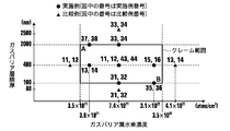
- FIG. 6 and FIG. 7 plots data of an example and a comparative example in which the material of the protective insulating layer is silicon nitride
- FIG. 7 plots data of an example and a comparative example using silicon oxide.
- the point ⁇ represents the example, and the point ⁇ represents the comparative example.
- the numbers written beside each point indicate the example or comparative example number.
- region enclosed with the square in each figure is an area
- the vicinity of B is a region where the protective insulating layer is thin and the hydrogen concentration in the protective insulating layer is the highest, so the threshold voltage is expected to be largely deviated from 0V. From the example, it can be seen that the threshold voltage is in a predetermined range. Moreover, it can be seen from the comparison between FIGS. 6 and 7 that the effective range does not change even if the material of the protective insulating layer is changed.
Landscapes
- Thin Film Transistor (AREA)
Priority Applications (1)
| Application Number | Priority Date | Filing Date | Title |
|---|---|---|---|
| KR1020157027464A KR101778874B1 (ko) | 2013-03-08 | 2014-01-24 | 산화물 반도체 박막 트랜지스터용 기판 |
Applications Claiming Priority (2)
| Application Number | Priority Date | Filing Date | Title |
|---|---|---|---|
| JP2013046827A JP5936568B2 (ja) | 2013-03-08 | 2013-03-08 | 酸化物半導体薄膜トランジスタ用基板およびその基板を用いた半導体装置 |
| JP2013-046827 | 2013-03-08 |
Publications (1)
| Publication Number | Publication Date |
|---|---|
| WO2014136375A1 true WO2014136375A1 (ja) | 2014-09-12 |
Family
ID=51490914
Family Applications (1)
| Application Number | Title | Priority Date | Filing Date |
|---|---|---|---|
| PCT/JP2014/000354 Ceased WO2014136375A1 (ja) | 2013-03-08 | 2014-01-24 | 酸化物半導体薄膜トランジスタ用基板 |
Country Status (3)
| Country | Link |
|---|---|
| JP (1) | JP5936568B2 (enExample) |
| KR (1) | KR101778874B1 (enExample) |
| WO (1) | WO2014136375A1 (enExample) |
Cited By (1)
| Publication number | Priority date | Publication date | Assignee | Title |
|---|---|---|---|---|
| CN112114460A (zh) * | 2020-09-23 | 2020-12-22 | 北海惠科光电技术有限公司 | 基于阵列基板的绝缘单元及其制备方法、阵列基板及其制备方法、显示机构 |
Families Citing this family (2)
| Publication number | Priority date | Publication date | Assignee | Title |
|---|---|---|---|---|
| TWI809075B (zh) * | 2018-03-30 | 2023-07-21 | 美商非結晶公司 | 電子裝置及具有其之顯示器 |
| KR102299087B1 (ko) | 2019-08-09 | 2021-09-08 | 김 철 환 | 광섬유사가 내장되어서 발광하는 혈관 및 피하용 카테터 |
Citations (4)
| Publication number | Priority date | Publication date | Assignee | Title |
|---|---|---|---|---|
| JP2011159807A (ja) * | 2010-02-01 | 2011-08-18 | Fujifilm Corp | 絶縁性金属基板および半導体装置 |
| JP2011181895A (ja) * | 2010-02-08 | 2011-09-15 | Fujifilm Corp | 絶縁層付金属基板およびその製造方法、半導体装置およびその製造方法ならびに太陽電池およびその製造方法 |
| JP2012094757A (ja) * | 2010-10-28 | 2012-05-17 | Fujifilm Corp | 薄膜トランジスタおよびその製造方法 |
| JP2013044000A (ja) * | 2011-08-22 | 2013-03-04 | Fujifilm Corp | 絶縁層付金属基板およびその製造方法、半導体装置およびその製造方法、太陽電池およびその製造方法、電子回路およびその製造方法、ならびに発光素子およびその製造方法 |
Family Cites Families (4)
| Publication number | Priority date | Publication date | Assignee | Title |
|---|---|---|---|---|
| JP2006196851A (ja) | 2004-12-16 | 2006-07-27 | Toppan Printing Co Ltd | 薄膜トランジスタ及びその製造方法 |
| US9129801B2 (en) | 2009-06-16 | 2015-09-08 | Basf Se | Thermally labile precursor compounds for improving the interparticulate contact sites and for filling the interstices in semiconductive metal oxide particle layers |
| JP5394867B2 (ja) * | 2009-09-17 | 2014-01-22 | 富士フイルム株式会社 | ガスバリア膜およびガスバリアフィルム |
| JP2011249674A (ja) * | 2010-05-28 | 2011-12-08 | Fujifilm Corp | 薄膜トランジスタおよびその製造方法 |
-
2013
- 2013-03-08 JP JP2013046827A patent/JP5936568B2/ja active Active
-
2014
- 2014-01-24 WO PCT/JP2014/000354 patent/WO2014136375A1/ja not_active Ceased
- 2014-01-24 KR KR1020157027464A patent/KR101778874B1/ko active Active
Patent Citations (4)
| Publication number | Priority date | Publication date | Assignee | Title |
|---|---|---|---|---|
| JP2011159807A (ja) * | 2010-02-01 | 2011-08-18 | Fujifilm Corp | 絶縁性金属基板および半導体装置 |
| JP2011181895A (ja) * | 2010-02-08 | 2011-09-15 | Fujifilm Corp | 絶縁層付金属基板およびその製造方法、半導体装置およびその製造方法ならびに太陽電池およびその製造方法 |
| JP2012094757A (ja) * | 2010-10-28 | 2012-05-17 | Fujifilm Corp | 薄膜トランジスタおよびその製造方法 |
| JP2013044000A (ja) * | 2011-08-22 | 2013-03-04 | Fujifilm Corp | 絶縁層付金属基板およびその製造方法、半導体装置およびその製造方法、太陽電池およびその製造方法、電子回路およびその製造方法、ならびに発光素子およびその製造方法 |
Cited By (2)
| Publication number | Priority date | Publication date | Assignee | Title |
|---|---|---|---|---|
| CN112114460A (zh) * | 2020-09-23 | 2020-12-22 | 北海惠科光电技术有限公司 | 基于阵列基板的绝缘单元及其制备方法、阵列基板及其制备方法、显示机构 |
| CN112114460B (zh) * | 2020-09-23 | 2022-12-23 | 北海惠科光电技术有限公司 | 基于阵列基板的绝缘单元及其制备方法、阵列基板及其制备方法、显示机构 |
Also Published As
| Publication number | Publication date |
|---|---|
| KR101778874B1 (ko) | 2017-09-14 |
| KR20150129767A (ko) | 2015-11-20 |
| JP2014175464A (ja) | 2014-09-22 |
| JP5936568B2 (ja) | 2016-06-22 |
Similar Documents
| Publication | Publication Date | Title |
|---|---|---|
| US9224839B2 (en) | Method for manufacturing semiconductor device | |
| TWI496197B (zh) | Wiring structure | |
| US8222158B2 (en) | Electronic device, method of manufacturing the same, display and sensor | |
| KR101919212B1 (ko) | 박막 트랜지스터 | |
| JP5520084B2 (ja) | 電界効果型トランジスタの製造方法 | |
| KR101795194B1 (ko) | 박막 트랜지스터 및 그의 제조 방법 | |
| US9024322B2 (en) | Wiring structure and display device | |
| US10121898B2 (en) | Thin-film transistor substrate and method of manufacturing the same | |
| US8680526B2 (en) | Electronic device, method of producing the same, and display device | |
| JP6357665B2 (ja) | 薄膜トランジスタ基板及びその製造方法 | |
| WO2012124444A1 (ja) | 薄膜トランジスタの製造方法、薄膜トランジスタ、表示装置、センサ及びx線デジタル撮影装置 | |
| JP5437776B2 (ja) | 酸化物半導体を用いた薄膜トランジスタおよびその製造方法 | |
| KR101132989B1 (ko) | 박막 트랜지스터의 제조 방법 및 전기 광학 장치의 제조 방법 | |
| JP5936568B2 (ja) | 酸化物半導体薄膜トランジスタ用基板およびその基板を用いた半導体装置 | |
| TW201813003A (zh) | 薄膜電晶體 | |
| US20110006298A1 (en) | Electronic device and method for producing the same | |
| JP6550514B2 (ja) | ディスプレイ用酸化物半導体薄膜、ディスプレイ用薄膜トランジスタ及びディスプレイ用スパッタリングターゲット | |
| TWI541900B (zh) | 絕緣膜及其製造方法 | |
| WO2016035554A1 (ja) | 薄膜トランジスタの酸化物半導体薄膜、薄膜トランジスタ、およびスパッタリングターゲット | |
| US20200357924A1 (en) | Oxide semiconductor thin film | |
| WO2019107043A1 (ja) | 酸化物半導体薄膜、薄膜トランジスタ及びスパッタリングターゲット | |
| JP2011091365A (ja) | 配線構造およびその製造方法、並びに配線構造を備えた表示装置 | |
| WO2012173035A1 (ja) | 半導体装置およびその製造方法 |
Legal Events
| Date | Code | Title | Description |
|---|---|---|---|
| 121 | Ep: the epo has been informed by wipo that ep was designated in this application |
Ref document number: 14760558 Country of ref document: EP Kind code of ref document: A1 |
|
| NENP | Non-entry into the national phase |
Ref country code: DE |
|
| ENP | Entry into the national phase |
Ref document number: 20157027464 Country of ref document: KR Kind code of ref document: A |
|
| 122 | Ep: pct application non-entry in european phase |
Ref document number: 14760558 Country of ref document: EP Kind code of ref document: A1 |