WO2014136375A1 - 酸化物半導体薄膜トランジスタ用基板 - Google Patents
酸化物半導体薄膜トランジスタ用基板 Download PDFInfo
- Publication number
- WO2014136375A1 WO2014136375A1 PCT/JP2014/000354 JP2014000354W WO2014136375A1 WO 2014136375 A1 WO2014136375 A1 WO 2014136375A1 JP 2014000354 W JP2014000354 W JP 2014000354W WO 2014136375 A1 WO2014136375 A1 WO 2014136375A1
- Authority
- WO
- WIPO (PCT)
- Prior art keywords
- oxide semiconductor
- insulating layer
- protective insulating
- layer
- substrate
- Prior art date
Links
- 239000004065 semiconductor Substances 0.000 title claims abstract description 237
- 239000000758 substrate Substances 0.000 title claims abstract description 121
- 239000010409 thin film Substances 0.000 title claims abstract description 103
- 239000000463 material Substances 0.000 claims abstract description 107
- 229910052751 metal Inorganic materials 0.000 claims abstract description 85
- 239000002184 metal Substances 0.000 claims abstract description 85
- 239000001257 hydrogen Substances 0.000 claims abstract description 62
- 229910052739 hydrogen Inorganic materials 0.000 claims abstract description 62
- UFHFLCQGNIYNRP-UHFFFAOYSA-N Hydrogen Chemical compound [H][H] UFHFLCQGNIYNRP-UHFFFAOYSA-N 0.000 claims abstract description 60
- 150000003377 silicon compounds Chemical class 0.000 claims abstract description 18
- 230000001681 protective effect Effects 0.000 claims description 168
- 239000010408 film Substances 0.000 claims description 134
- 238000000034 method Methods 0.000 claims description 52
- 238000004519 manufacturing process Methods 0.000 claims description 36
- 229910052782 aluminium Inorganic materials 0.000 claims description 30
- XAGFODPZIPBFFR-UHFFFAOYSA-N aluminium Chemical compound [Al] XAGFODPZIPBFFR-UHFFFAOYSA-N 0.000 claims description 28
- 229910052814 silicon oxide Inorganic materials 0.000 claims description 19
- VYPSYNLAJGMNEJ-UHFFFAOYSA-N Silicium dioxide Chemical compound O=[Si]=O VYPSYNLAJGMNEJ-UHFFFAOYSA-N 0.000 claims description 17
- 229910052581 Si3N4 Inorganic materials 0.000 claims description 16
- HQVNEWCFYHHQES-UHFFFAOYSA-N silicon nitride Chemical compound N12[Si]34N5[Si]62N3[Si]51N64 HQVNEWCFYHHQES-UHFFFAOYSA-N 0.000 claims description 16
- 238000005268 plasma chemical vapour deposition Methods 0.000 claims description 15
- 229910052733 gallium Inorganic materials 0.000 claims description 12
- 229910052738 indium Inorganic materials 0.000 claims description 12
- 229910052725 zinc Inorganic materials 0.000 claims description 11
- 230000002829 reductive effect Effects 0.000 claims description 8
- XUIMIQQOPSSXEZ-UHFFFAOYSA-N Silicon Chemical compound [Si] XUIMIQQOPSSXEZ-UHFFFAOYSA-N 0.000 claims description 6
- 239000012298 atmosphere Substances 0.000 claims description 6
- 239000010703 silicon Substances 0.000 claims description 6
- 229910052710 silicon Inorganic materials 0.000 claims description 5
- 229910000838 Al alloy Inorganic materials 0.000 claims description 2
- 125000004429 atom Chemical group 0.000 abstract description 23
- 125000004435 hydrogen atom Chemical class [H]* 0.000 abstract description 2
- 239000010410 layer Substances 0.000 description 372
- 239000002585 base Substances 0.000 description 138
- 230000000052 comparative effect Effects 0.000 description 64
- 239000007789 gas Substances 0.000 description 60
- 230000015572 biosynthetic process Effects 0.000 description 43
- 238000005530 etching Methods 0.000 description 25
- 238000004544 sputter deposition Methods 0.000 description 20
- 238000011156 evaluation Methods 0.000 description 15
- 239000000243 solution Substances 0.000 description 14
- MUBZPKHOEPUJKR-UHFFFAOYSA-N Oxalic acid Chemical compound OC(=O)C(O)=O MUBZPKHOEPUJKR-UHFFFAOYSA-N 0.000 description 12
- XLOMVQKBTHCTTD-UHFFFAOYSA-N Zinc monoxide Chemical compound [Zn]=O XLOMVQKBTHCTTD-UHFFFAOYSA-N 0.000 description 12
- 150000002500 ions Chemical class 0.000 description 12
- 239000000126 substance Substances 0.000 description 11
- 239000011701 zinc Substances 0.000 description 11
- 238000007743 anodising Methods 0.000 description 10
- 238000005452 bending Methods 0.000 description 10
- 230000000694 effects Effects 0.000 description 10
- 239000011521 glass Substances 0.000 description 10
- 229910045601 alloy Inorganic materials 0.000 description 9
- 239000000956 alloy Substances 0.000 description 9
- 230000004888 barrier function Effects 0.000 description 9
- 238000005259 measurement Methods 0.000 description 9
- 239000000203 mixture Substances 0.000 description 9
- 229910052750 molybdenum Inorganic materials 0.000 description 9
- 238000007872 degassing Methods 0.000 description 8
- 238000009413 insulation Methods 0.000 description 8
- 230000002411 adverse Effects 0.000 description 7
- 239000011148 porous material Substances 0.000 description 7
- 239000011347 resin Substances 0.000 description 7
- 229920005989 resin Polymers 0.000 description 7
- 238000012360 testing method Methods 0.000 description 7
- 239000011787 zinc oxide Substances 0.000 description 7
- QTBSBXVTEAMEQO-UHFFFAOYSA-N Acetic acid Chemical compound CC(O)=O QTBSBXVTEAMEQO-UHFFFAOYSA-N 0.000 description 6
- LFQSCWFLJHTTHZ-UHFFFAOYSA-N Ethanol Chemical compound CCO LFQSCWFLJHTTHZ-UHFFFAOYSA-N 0.000 description 6
- 229910001182 Mo alloy Inorganic materials 0.000 description 6
- 238000000137 annealing Methods 0.000 description 6
- 229910044991 metal oxide Inorganic materials 0.000 description 6
- 150000004706 metal oxides Chemical class 0.000 description 6
- 239000010955 niobium Substances 0.000 description 6
- 229910001220 stainless steel Inorganic materials 0.000 description 6
- 239000010936 titanium Substances 0.000 description 6
- 229910004298 SiO 2 Inorganic materials 0.000 description 5
- 239000002253 acid Substances 0.000 description 5
- 238000000576 coating method Methods 0.000 description 5
- 238000007733 ion plating Methods 0.000 description 5
- 238000000206 photolithography Methods 0.000 description 5
- 238000000053 physical method Methods 0.000 description 5
- 238000007639 printing Methods 0.000 description 5
- 239000000523 sample Substances 0.000 description 5
- 239000010935 stainless steel Substances 0.000 description 5
- 238000001771 vacuum deposition Methods 0.000 description 5
- XLYOFNOQVPJJNP-UHFFFAOYSA-N water Chemical compound O XLYOFNOQVPJJNP-UHFFFAOYSA-N 0.000 description 5
- ZOKXTWBITQBERF-UHFFFAOYSA-N Molybdenum Chemical compound [Mo] ZOKXTWBITQBERF-UHFFFAOYSA-N 0.000 description 4
- QAOWNCQODCNURD-UHFFFAOYSA-N Sulfuric acid Chemical compound OS(O)(=O)=O QAOWNCQODCNURD-UHFFFAOYSA-N 0.000 description 4
- 238000003917 TEM image Methods 0.000 description 4
- 238000004458 analytical method Methods 0.000 description 4
- 239000000969 carrier Substances 0.000 description 4
- -1 cesium ions Chemical class 0.000 description 4
- 230000008859 change Effects 0.000 description 4
- 150000001875 compounds Chemical class 0.000 description 4
- 239000000470 constituent Substances 0.000 description 4
- 239000010949 copper Substances 0.000 description 4
- 238000001312 dry etching Methods 0.000 description 4
- 239000011777 magnesium Substances 0.000 description 4
- 239000011733 molybdenum Substances 0.000 description 4
- 229910052758 niobium Inorganic materials 0.000 description 4
- 235000006408 oxalic acid Nutrition 0.000 description 4
- VLTRZXGMWDSKGL-UHFFFAOYSA-N perchloric acid Chemical compound OCl(=O)(=O)=O VLTRZXGMWDSKGL-UHFFFAOYSA-N 0.000 description 4
- 230000008569 process Effects 0.000 description 4
- 229910052715 tantalum Inorganic materials 0.000 description 4
- 229910052719 titanium Inorganic materials 0.000 description 4
- 229960001296 zinc oxide Drugs 0.000 description 4
- 238000002441 X-ray diffraction Methods 0.000 description 3
- 239000003513 alkali Substances 0.000 description 3
- 239000007864 aqueous solution Substances 0.000 description 3
- 229910052792 caesium Inorganic materials 0.000 description 3
- 238000005229 chemical vapour deposition Methods 0.000 description 3
- 230000008602 contraction Effects 0.000 description 3
- 238000000151 deposition Methods 0.000 description 3
- 238000009792 diffusion process Methods 0.000 description 3
- 229910001195 gallium oxide Inorganic materials 0.000 description 3
- 239000012535 impurity Substances 0.000 description 3
- 239000012212 insulator Substances 0.000 description 3
- 230000003647 oxidation Effects 0.000 description 3
- 238000007254 oxidation reaction Methods 0.000 description 3
- 239000001301 oxygen Substances 0.000 description 3
- 229910052760 oxygen Inorganic materials 0.000 description 3
- 238000001020 plasma etching Methods 0.000 description 3
- 238000004528 spin coating Methods 0.000 description 3
- YVTHLONGBIQYBO-UHFFFAOYSA-N zinc indium(3+) oxygen(2-) Chemical compound [O--].[Zn++].[In+3] YVTHLONGBIQYBO-UHFFFAOYSA-N 0.000 description 3
- RYGMFSIKBFXOCR-UHFFFAOYSA-N Copper Chemical compound [Cu] RYGMFSIKBFXOCR-UHFFFAOYSA-N 0.000 description 2
- XEEYBQQBJWHFJM-UHFFFAOYSA-N Iron Chemical compound [Fe] XEEYBQQBJWHFJM-UHFFFAOYSA-N 0.000 description 2
- FYYHWMGAXLPEAU-UHFFFAOYSA-N Magnesium Chemical compound [Mg] FYYHWMGAXLPEAU-UHFFFAOYSA-N 0.000 description 2
- GRYLNZFGIOXLOG-UHFFFAOYSA-N Nitric acid Chemical compound O[N+]([O-])=O GRYLNZFGIOXLOG-UHFFFAOYSA-N 0.000 description 2
- NBIIXXVUZAFLBC-UHFFFAOYSA-N Phosphoric acid Chemical compound OP(O)(O)=O NBIIXXVUZAFLBC-UHFFFAOYSA-N 0.000 description 2
- 229910000831 Steel Inorganic materials 0.000 description 2
- RTAQQCXQSZGOHL-UHFFFAOYSA-N Titanium Chemical compound [Ti] RTAQQCXQSZGOHL-UHFFFAOYSA-N 0.000 description 2
- 150000007513 acids Chemical class 0.000 description 2
- 239000010407 anodic oxide Substances 0.000 description 2
- 238000002048 anodisation reaction Methods 0.000 description 2
- QVGXLLKOCUKJST-UHFFFAOYSA-N atomic oxygen Chemical compound [O] QVGXLLKOCUKJST-UHFFFAOYSA-N 0.000 description 2
- 229910052804 chromium Inorganic materials 0.000 description 2
- 239000004020 conductor Substances 0.000 description 2
- 229910052802 copper Inorganic materials 0.000 description 2
- 239000013527 degreasing agent Substances 0.000 description 2
- 238000005237 degreasing agent Methods 0.000 description 2
- 230000008021 deposition Effects 0.000 description 2
- 238000010586 diagram Methods 0.000 description 2
- AJNVQOSZGJRYEI-UHFFFAOYSA-N digallium;oxygen(2-) Chemical compound [O-2].[O-2].[O-2].[Ga+3].[Ga+3] AJNVQOSZGJRYEI-UHFFFAOYSA-N 0.000 description 2
- 238000004090 dissolution Methods 0.000 description 2
- 238000005868 electrolysis reaction Methods 0.000 description 2
- 238000005516 engineering process Methods 0.000 description 2
- 229910052737 gold Inorganic materials 0.000 description 2
- 238000010438 heat treatment Methods 0.000 description 2
- 229910003437 indium oxide Inorganic materials 0.000 description 2
- PJXISJQVUVHSOJ-UHFFFAOYSA-N indium(iii) oxide Chemical compound [O-2].[O-2].[O-2].[In+3].[In+3] PJXISJQVUVHSOJ-UHFFFAOYSA-N 0.000 description 2
- AMGQUBHHOARCQH-UHFFFAOYSA-N indium;oxotin Chemical compound [In].[Sn]=O AMGQUBHHOARCQH-UHFFFAOYSA-N 0.000 description 2
- 238000003475 lamination Methods 0.000 description 2
- 239000004973 liquid crystal related substance Substances 0.000 description 2
- 229910052749 magnesium Inorganic materials 0.000 description 2
- 230000000873 masking effect Effects 0.000 description 2
- 150000002739 metals Chemical class 0.000 description 2
- GUCVJGMIXFAOAE-UHFFFAOYSA-N niobium atom Chemical compound [Nb] GUCVJGMIXFAOAE-UHFFFAOYSA-N 0.000 description 2
- 229910017604 nitric acid Inorganic materials 0.000 description 2
- 230000002265 prevention Effects 0.000 description 2
- 239000011241 protective layer Substances 0.000 description 2
- 238000001552 radio frequency sputter deposition Methods 0.000 description 2
- 239000002994 raw material Substances 0.000 description 2
- 238000001004 secondary ion mass spectrometry Methods 0.000 description 2
- VSZWPYCFIRKVQL-UHFFFAOYSA-N selanylidenegallium;selenium Chemical compound [Se].[Se]=[Ga].[Se]=[Ga] VSZWPYCFIRKVQL-UHFFFAOYSA-N 0.000 description 2
- 230000035945 sensitivity Effects 0.000 description 2
- 239000002356 single layer Substances 0.000 description 2
- 239000010959 steel Substances 0.000 description 2
- GUVRBAGPIYLISA-UHFFFAOYSA-N tantalum atom Chemical compound [Ta] GUVRBAGPIYLISA-UHFFFAOYSA-N 0.000 description 2
- XOLBLPGZBRYERU-UHFFFAOYSA-N tin dioxide Chemical compound O=[Sn]=O XOLBLPGZBRYERU-UHFFFAOYSA-N 0.000 description 2
- 229910001887 tin oxide Inorganic materials 0.000 description 2
- 239000004925 Acrylic resin Substances 0.000 description 1
- 229920000178 Acrylic resin Polymers 0.000 description 1
- 229910018072 Al 2 O 3 Inorganic materials 0.000 description 1
- 229920000049 Carbon (fiber) Polymers 0.000 description 1
- BOTDANWDWHJENH-UHFFFAOYSA-N Tetraethyl orthosilicate Chemical compound CCO[Si](OCC)(OCC)OCC BOTDANWDWHJENH-UHFFFAOYSA-N 0.000 description 1
- GWEVSGVZZGPLCZ-UHFFFAOYSA-N Titan oxide Chemical compound O=[Ti]=O GWEVSGVZZGPLCZ-UHFFFAOYSA-N 0.000 description 1
- 229910007541 Zn O Inorganic materials 0.000 description 1
- GPFIZJURHXINSQ-UHFFFAOYSA-N acetic acid;nitric acid Chemical compound CC(O)=O.O[N+]([O-])=O GPFIZJURHXINSQ-UHFFFAOYSA-N 0.000 description 1
- IZQZNLBFNMTRMF-UHFFFAOYSA-N acetic acid;phosphoric acid Chemical compound CC(O)=O.OP(O)(O)=O IZQZNLBFNMTRMF-UHFFFAOYSA-N 0.000 description 1
- 230000002378 acidificating effect Effects 0.000 description 1
- 239000000853 adhesive Substances 0.000 description 1
- 230000001070 adhesive effect Effects 0.000 description 1
- 229910000147 aluminium phosphate Inorganic materials 0.000 description 1
- 238000004380 ashing Methods 0.000 description 1
- 239000011230 binding agent Substances 0.000 description 1
- 239000004917 carbon fiber Substances 0.000 description 1
- 230000015556 catabolic process Effects 0.000 description 1
- 238000006243 chemical reaction Methods 0.000 description 1
- 238000005097 cold rolling Methods 0.000 description 1
- 238000005336 cracking Methods 0.000 description 1
- 239000013078 crystal Substances 0.000 description 1
- 238000002425 crystallisation Methods 0.000 description 1
- 230000008025 crystallization Effects 0.000 description 1
- 238000006731 degradation reaction Methods 0.000 description 1
- 238000001514 detection method Methods 0.000 description 1
- 230000006866 deterioration Effects 0.000 description 1
- 238000010292 electrical insulation Methods 0.000 description 1
- 239000003792 electrolyte Substances 0.000 description 1
- LUCJEPREDVDXKU-UHFFFAOYSA-N ethene silane Chemical compound [SiH4].C=C LUCJEPREDVDXKU-UHFFFAOYSA-N 0.000 description 1
- 230000002349 favourable effect Effects 0.000 description 1
- 239000010419 fine particle Substances 0.000 description 1
- BHEPBYXIRTUNPN-UHFFFAOYSA-N hydridophosphorus(.) (triplet) Chemical compound [PH] BHEPBYXIRTUNPN-UHFFFAOYSA-N 0.000 description 1
- 150000002431 hydrogen Chemical class 0.000 description 1
- 238000011835 investigation Methods 0.000 description 1
- 239000007788 liquid Substances 0.000 description 1
- 238000001755 magnetron sputter deposition Methods 0.000 description 1
- VNWKTOKETHGBQD-UHFFFAOYSA-N methane Chemical compound C VNWKTOKETHGBQD-UHFFFAOYSA-N 0.000 description 1
- 238000002156 mixing Methods 0.000 description 1
- 239000003960 organic solvent Substances 0.000 description 1
- ZDYUUBIMAGBMPY-UHFFFAOYSA-N oxalic acid;hydrate Chemical compound O.OC(=O)C(O)=O ZDYUUBIMAGBMPY-UHFFFAOYSA-N 0.000 description 1
- TWNQGVIAIRXVLR-UHFFFAOYSA-N oxo(oxoalumanyloxy)alumane Chemical compound O=[Al]O[Al]=O TWNQGVIAIRXVLR-UHFFFAOYSA-N 0.000 description 1
- 230000036961 partial effect Effects 0.000 description 1
- 238000000059 patterning Methods 0.000 description 1
- 230000035699 permeability Effects 0.000 description 1
- 239000012466 permeate Substances 0.000 description 1
- 238000000623 plasma-assisted chemical vapour deposition Methods 0.000 description 1
- 229920000767 polyaniline Polymers 0.000 description 1
- 229920001721 polyimide Polymers 0.000 description 1
- 239000009719 polyimide resin Substances 0.000 description 1
- 229920000128 polypyrrole Polymers 0.000 description 1
- 229920000123 polythiophene Polymers 0.000 description 1
- 238000002360 preparation method Methods 0.000 description 1
- 238000012545 processing Methods 0.000 description 1
- 239000013074 reference sample Substances 0.000 description 1
- 230000003014 reinforcing effect Effects 0.000 description 1
- 238000007788 roughening Methods 0.000 description 1
- 238000001179 sorption measurement Methods 0.000 description 1
- 230000003746 surface roughness Effects 0.000 description 1
- OGIDPMRJRNCKJF-UHFFFAOYSA-N titanium oxide Inorganic materials [Ti]=O OGIDPMRJRNCKJF-UHFFFAOYSA-N 0.000 description 1
- 230000000007 visual effect Effects 0.000 description 1
- 238000005406 washing Methods 0.000 description 1
Images


Classifications
-
- H—ELECTRICITY
- H01—ELECTRIC ELEMENTS
- H01L—SEMICONDUCTOR DEVICES NOT COVERED BY CLASS H10
- H01L29/00—Semiconductor devices specially adapted for rectifying, amplifying, oscillating or switching and having potential barriers; Capacitors or resistors having potential barriers, e.g. a PN-junction depletion layer or carrier concentration layer; Details of semiconductor bodies or of electrodes thereof ; Multistep manufacturing processes therefor
- H01L29/66—Types of semiconductor device ; Multistep manufacturing processes therefor
- H01L29/68—Types of semiconductor device ; Multistep manufacturing processes therefor controllable by only the electric current supplied, or only the electric potential applied, to an electrode which does not carry the current to be rectified, amplified or switched
- H01L29/76—Unipolar devices, e.g. field effect transistors
- H01L29/772—Field effect transistors
- H01L29/78—Field effect transistors with field effect produced by an insulated gate
- H01L29/786—Thin film transistors, i.e. transistors with a channel being at least partly a thin film
- H01L29/78603—Thin film transistors, i.e. transistors with a channel being at least partly a thin film characterised by the insulating substrate or support
-
- H—ELECTRICITY
- H01—ELECTRIC ELEMENTS
- H01L—SEMICONDUCTOR DEVICES NOT COVERED BY CLASS H10
- H01L29/00—Semiconductor devices specially adapted for rectifying, amplifying, oscillating or switching and having potential barriers; Capacitors or resistors having potential barriers, e.g. a PN-junction depletion layer or carrier concentration layer; Details of semiconductor bodies or of electrodes thereof ; Multistep manufacturing processes therefor
- H01L29/66—Types of semiconductor device ; Multistep manufacturing processes therefor
- H01L29/68—Types of semiconductor device ; Multistep manufacturing processes therefor controllable by only the electric current supplied, or only the electric potential applied, to an electrode which does not carry the current to be rectified, amplified or switched
- H01L29/76—Unipolar devices, e.g. field effect transistors
- H01L29/772—Field effect transistors
- H01L29/78—Field effect transistors with field effect produced by an insulated gate
- H01L29/786—Thin film transistors, i.e. transistors with a channel being at least partly a thin film
- H01L29/7869—Thin film transistors, i.e. transistors with a channel being at least partly a thin film having a semiconductor body comprising an oxide semiconductor material, e.g. zinc oxide, copper aluminium oxide, cadmium stannate
Definitions
- the present invention relates to a substrate used for an oxide semiconductor thin film transistor that can be used in a flexible device such as a display device using liquid crystal or an organic EL element, electronic paper, or an X-ray sensor, a semiconductor device, and a manufacturing method thereof.
- Patent Document 1 a thin film transistor (TFT) using an In—Ga—Zn—O-based oxide semiconductor (InGaZnO) as an active layer can be formed at a relatively low temperature, and a resin substrate can be used. For this reason, it is described that this is a technique suitable for making a flat panel display (FPD) thinner, lighter, and flexible.
- FPD flat panel display
- the threshold voltage of the oxide semiconductor thin film transistor is greatly deviated from 0V. It is disclosed that the problem can be solved by providing a protective layer on the protective layer.
- Patent Document 1 also describes that not only a resin substrate but also a metal substrate such as aluminum whose surface is insulated may be used.
- Patent Document 2 is a patent document relating to a flexible substrate, which has higher heat resistance than a resin substrate by forming an aluminum oxide insulating layer having a porous (porous) structure by anodizing treatment on a metal surface, It is disclosed that a flexible substrate that is excellent in thermal dimensional stability and does not cause a failure such as a short circuit can be obtained.
- Patent Document 3 is a patent document relating to a resin-made flexible substrate, and a gas barrier layer containing a silicon compound is provided on the surface of the resin substrate in order to reduce the permeated gas that permeates the resin substrate.
- a gas barrier layer containing a silicon compound is provided on the surface of the resin substrate in order to reduce the permeated gas that permeates the resin substrate.
- Patent Document 1 describes that a TFT may be manufactured using a metal substrate whose surface is insulated.
- a specific example of the metal substrate and a mode and a specific example of a TFT manufactured using the metal substrate are not described.
- an oxide semiconductor thin film transistor having a configuration described in Patent Document 1 was formed on a metal substrate having a porous aluminum anodized insulating film described in Patent Document 2.
- the manufactured oxide semiconductor thin film transistor does not operate normally. Specifically, the mobility and threshold voltage of the oxide semiconductor thin film transistor did not fall within a predetermined range despite the use of a metal substrate that is expected to have high heat resistance and high gas barrier properties.
- the threshold voltage is slightly minus near zero volts, and is preferably turned off in a state where a slightly negative bias is applied.
- the present invention has been made in view of the above circumstances, a substrate for a flexible oxide semiconductor thin film transistor capable of forming an oxide semiconductor thin film transistor having high mobility and a threshold voltage within a predetermined range, and a substrate for the same.
- a flexible semiconductor device obtained by use is provided.
- the present inventors have adsorbed gas to the porous layer on the surface of the anodized aluminum substrate because the time required for evacuation is long when an aluminum substrate having a porous anodized insulating film is put into a vacuum apparatus. It was speculated that the threshold voltage of the InGaZnO-TFT was greatly changed from 0 V because the adsorbed gas was released during the production or diffused after the production.
- an anodized aluminum substrate provided with a gas barrier layer described in Patent Document 3 was prepared, and an oxide semiconductor thin film transistor was formed thereon to manufacture an oxide semiconductor device.
- a semiconductor device having desired characteristics still cannot be obtained.
- the surface roughness of the anodized aluminum substrate is large, and therefore the gas barrier layer described in Patent Document 3 has one reason that the substrate surface coverage is not sufficient. I understood. Therefore, as a result of further detailed examination of the film configuration of the substrate and the manufacturing method, the above problems have been finally solved and the present invention has been completed.
- a substrate for a flexible oxide semiconductor thin film transistor includes a base material provided with a porous layer formed on at least one surface of a metal base, and the porous layer. And a protective insulating layer containing hydrogen as a main component and containing hydrogen, and the hydrogen concentration in the protective insulating layer is 3.5 ⁇ 10 21 atoms / cm 3 or more and 3.5 ⁇ 10 It is 22 atoms / cm 3 or less, and the thickness of the protective insulating layer is 100 nm or more and 2000 nm or less.
- the silicon compound is preferably at least one selected from silicon nitride, silicon oxide, and silicon oxynitride.
- the porous layer is preferably an anodic oxide film of aluminum or aluminum alloy. Furthermore, the porous layer is preferably formed on both surfaces of the metal base.
- the protective insulating layer is preferably provided at least over the entire region where the active layer formed of an oxide semiconductor is formed.
- the active layer made of an oxide semiconductor preferably contains In, Ga, and Zn.
- the active layer made of an oxide semiconductor is preferably amorphous.
- An oxide semiconductor thin film transistor has at least a gate electrode, a gate insulating film, an active layer made of an oxide semiconductor, a source and a drain electrode.
- the oxide semiconductor thin film transistor is preferably formed over a substrate and includes at least a gate electrode, a gate insulating film, an active layer made of an oxide semiconductor, and a source and drain electrodes in this order. Furthermore, it is preferable that the gate insulating film of the oxide semiconductor thin film transistor has silicon oxide as a main component.
- the method for producing a flexible semiconductor device of the present invention provides a base material having a porous layer on at least one surface on a metal base, and a silicon compound as a main component on at least a part of the porous layer,
- a protective insulating layer having a hydrogen concentration of 3.5 ⁇ 10 21 atoms / cm 3 or more and 3.5 ⁇ 10 22 atoms / cm 3 or less and a thickness of 100 nm or more and 2000 nm or less is formed by plasma CVD (CVD: Chemical Vapor).
- CVD Chemical Vapor
- the substrate having the porous layer before forming the protective insulating layer, it is preferable to heat the substrate having the porous layer under reduced pressure from the atmosphere at 350 ° C. or higher.
- a layer that is provided on the porous layer and mainly contains a silicon compound is referred to as a protective insulating layer.
- main component means that 60% by mass or more of the material constituting the layer is composed of the specified compound.
- an “oxide semiconductor thin film transistor” means a thin film transistor having at least a gate electrode, a gate insulating film, an active layer made of an oxide semiconductor, and source / drain electrodes.
- ... is provided in direct contact with the surface of It shall include both cases where another layer exists and is provided on that layer. Further, in that case,... May be provided in the whole area of ⁇ , or may be provided only in part.
- the substrate for an oxide semiconductor thin film transistor of the present invention includes a porous layer on the surface of the metal base, and further includes a protective insulating layer containing a silicon compound as a main component and containing hydrogen on the porous layer,
- the hydrogen concentration in the protective insulating layer is 3.5 ⁇ 10 21 atoms / cm 3 or more and 3.5 ⁇ 10 22 atoms / cm 3 or less, and the thickness of the protective insulating layer is 100 nm or more and 2000 nm or less.
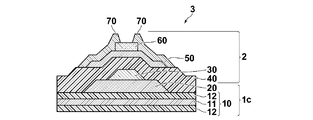
- FIG. 1 is a diagram schematically showing an embodiment of a flexible semiconductor device.
- a flexible oxide semiconductor thin film transistor substrate 1 a includes a base material 10 and a protective insulating layer 20 provided on the base material 10.
- the substrate 10 includes a metal base 11 and a porous layer 12 provided thereon.
- the porous layer 12 is located between the metal base 11 and the protective insulating layer provided thereon, and has a function of improving adhesion of the layer provided thereon by roughening the surface.
- the protective insulating layer 20 prevents the gas adsorbed on the surface of the porous layer 12 from being released into the manufacturing apparatus during the manufacturing process or adversely affecting the oxide semiconductor layer due to diffusion after the manufacturing. Have a role.
- the protective insulating layer 20 also has a role of preventing the base material 10 from being damaged by chemicals such as acid and alkali used, plasma during dry etching and sputtering film formation, and the like during the manufacturing process.
- the protective insulating layer 20 covers the porous layer 12 and has a silicon compound as a main component and a hydrogen concentration of 3.5 ⁇ 10 21 in order to ensure an adsorption gas release prevention function and a manufacturing process damage prevention function.
- a film thickness of atoms / cm 3 or more and 100 nm or more is required. Moreover, in order to ensure the flexibility of the base material 10 and to prevent the protective insulating layer 20 from cracking, the upper limit of the film thickness is 2000 nm.
- the characteristics of the oxide semiconductor thin film transistor are affected by the amount of hydrogen contained in the protective insulating layer 20.
- the protective insulating layer is formed so that the hydrogen concentration is 3.5 ⁇ 10 22 atoms / cm 3 or less.
- the protective insulating layer 20 has a hydrogen concentration set in a range of 3.5 ⁇ 10 21 atoms / cm 3 to 3.5 ⁇ 10 22 atoms / cm 3 and a thickness of 100 nm to 2000 nm.
- the active layer 50 is made of an oxide semiconductor containing at least one element selected from In, Ga, and Zn.
- Patent Document 1 it is known that the threshold voltage of an oxide semiconductor thin film transistor greatly deviates from around 0 V when the active layer is exposed to the atmosphere.
- the base material 10 having the metal base 11 reduces the intrusion of air and water vapor from the outside, the protective insulating layer 20 reduces the gas emission from the porous layer 12, and the protective insulating layer 20 itself also adversely affects the threshold voltage. Therefore, the threshold voltage of the oxide semiconductor thin film transistor is in the vicinity of 0V.
- the substrate the metal base, the porous layer, the protective insulating layer, and the oxide semiconductor thin film transistor will be described in order.
- the substrate 10 includes a metal base 11 and a porous layer 12 formed on at least one surface of the metal base.
- the base material 10 including the metal base 11 and the porous layer 12 is suitable as a flexible substrate for an oxide semiconductor thin film transistor because it has flexibility, gas barrier properties, and process resistance.
- the substrate 10 can be preferably used as long as it has at least the metal base 11 and the porous layer 12, but the metal base 11 is made of a clad material in which aluminum, stainless steel or a steel plate and an aluminum thin plate are integrated. Further, it is more preferable because the anodizing treatment of the aluminum thin plate is simplified and the durability of the base material is increased. Furthermore, in the base material obtained by anodizing the surface of the aluminum thin plate in the clad material in which both surfaces of the steel plate are sandwiched between the aluminum thin plates, the substrate caused by the difference in the thermal expansion coefficient of the material constituting the base material It is more preferable because warpage, film peeling, and the like can be suppressed.
- the substrate 10 provided with the porous layer 12 is preferably subjected to degassing treatment under reduced pressure before forming a protective insulating layer 20 described later.
- degassing treatment By carrying out the degassing treatment, the amount of gas adsorbed on the porous layer can be reduced, which is more preferable.
- a degassing process is performed by heating a substrate provided with a porous layer at 350 ° C. or higher while evacuating the chamber Can be implemented.
- the degassing treatment it is preferable to perform the degassing treatment with a film formation apparatus for forming the protective insulating layer 20 because the protective insulating layer can be provided without being exposed to the atmosphere after the degassing treatment. Further, it is more preferable to perform the treatment in the pretreatment chamber because the possibility that the released gas is taken in again when the protective insulating layer is formed can be reduced.
- This degassing treatment of the porous layer is preferably performed in as short a time as possible in order to avoid deterioration in productivity during mass production.
- the metal base 11 is at least partially made of metal and has a gas barrier property. Further, when a metal base having a thin plate shape is selected, it is preferable because flexibility can be provided while maintaining gas barrier properties.
- Examples of the material of the metal base 11 include aluminum (Al), iron (Fe), zirconium (Zr), titanium (Ti), magnesium (Mg), copper (Cu), niobium (Nb), and tantalum (Ta).
- a substrate containing at least one selected metal or an alloy of the above metals is preferred. Aluminum is preferable from the viewpoint of availability and light weight.
- the metal base 11 may be a single layer or a laminate of a plurality of layers, and the material may be a simple substance or an alloy. For example, for the purpose of adjusting expansion and contraction and warpage due to thermal expansion, it is possible to form a multilayer structure of multiple layers or use an alloy.
- the metal base refers to all portions excluding the porous layer.
- interposed into the porous of both surfaces shall be called a metal base.
- the metal base has a plurality of layers, at least one layer is made of metal.
- FIG. 2 shows an example in which the metal base 11 is composed of a plurality of layers.
- FIG. 2 shows a mode in which the metal base portion 11 has a three-layer configuration, and shows a configuration in which the auxiliary base portion 11a is sandwiched between the main base portions 11b.
- a laminated structure in which the auxiliary base portion 11a and the main base portion 11b are formed one by one is also suitable.
- at least one layer may be a metal, and the other layer may be a metal or not a metal.
- the material used for the metal base may be, for example, a stainless plate or a plate made of carbon fiber.
- the auxiliary base 11a may be employed for the purpose of adjusting the expansion / contraction rate, reinforcing the base material, and reducing the gas permeability.
- a metal thin plate is preferably used, and a stainless steel material is preferably used.
- the total thickness of the metal base 11 (the sum in the case where it is composed of a plurality of layers) can be appropriately selected depending on the application.
- Porous layer 12 is provided on the metal base 11.
- the porous layer 12 is provided on at least a part of the surface of the metal base, and can insulate the surface of the metal base 11 and improve the adhesion of the layer provided thereon by the anchor effect.
- the porous layer 12 is also excellent in the flexibility of the layer itself. From the viewpoint of flexibility, the pore diameter of the porous layer 12 is preferably about 10 nm.
- the porous layer 12 is preferably provided on one entire surface of the metal base, and more preferably on the entire both surfaces of the metal base. When a porous layer is provided equally on both surfaces of the metal base, it is more preferable that the stress becomes uniform and the substrate is less likely to warp.
- FIG. 1 and 2 show a mode in which the metal base 11 and the porous layer 12 are in direct contact with each other, but another layer may be provided between them as necessary.
- an insulating layer for further improving the insulating property of the metal base surface or an underlayer for easily attaching a porous layer may be provided.
- the material of the porous layer 12 is preferably an insulating metal oxide, and more preferably an oxide containing the same metal as the metal base 11.
- the porous layer 12 may be made by any manufacturing method, and a porous layer may be formed by applying a liquid in which insulating porous fine particles and a binder are dispersed to the surface of the metal base 11. May be formed into a porous layer.
- a mode in which a part of the metal base portion is anodized to form a porous layer is preferable.
- the thickness of the porous layer 12 can be appropriately selected depending on the application, but is preferably 0.1 ⁇ m to 100 ⁇ m, more preferably 0.5 ⁇ m to 50 ⁇ m, and more preferably 5 ⁇ m to 20 ⁇ m from the viewpoint of insulation and adhesion. Is most preferred.
- a layer made of a metal oxide is provided as the porous layer 12, it is preferable that the thickness is 50 ⁇ m or less because flexibility is easily secured. Further, it is preferable to set the thickness to 0.5 ⁇ m or more because insulation is easily secured.
- the method for forming the porous layer by the anodizing treatment is not particularly limited, and any method can be used as long as the anodized porous layer can be formed on the metal surface. Below, the porous layer formed by anodic oxidation is demonstrated.
- a method for producing a porous layer using anodization has been known as a simple method capable of forming nanometer-order pores.
- this porous layer is a metal oxide, it is known to have high insulation. Specifically, when a metal substrate is immersed in an acidic or alkaline electrolyte such as sulfuric acid, oxalic acid, or phosphoric acid, and this is used as an anode, oxidation and dissolution occur on the surface of the metal substrate. Simultaneously, an oxide film having pores on its surface can be formed.
- the metal for forming the porous layer using anodization can be selected as appropriate.
- At least one metal selected from copper (Cu), niobium (Nb) and tantalum (Ta), or an alloy of the above metals is preferable.
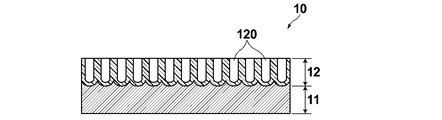
- FIG. 4 shows a schematic diagram of a porous layer obtained by anodizing treatment.
- FIG. 4 shows an embodiment in which a porous layer 12 is provided by anodizing only one side of the metal base 11.
- the surface to be treated of the metal base 11 is uniformly changed to a metal oxide, and nanometer-order pores 120 are formed. Since the surface to be treated is uniformly treated by the anodizing treatment, high insulation can be ensured.
- the porous layer is formed by treating the surface of the original metal base, the metal base 11 and the porous layer 12 are strongly bonded and do not easily peel off.
- the next layer (not shown) is formed on the porous layer, the components of the next layer enter the pores 120 at the time of film formation, so that adhesion is secured by a so-called anchor effect.
- the metal base made of the prepared metal or alloy is washed with water, it is degreased with a metal degreasing agent to remove dirt adhering to the surface, and the degreasing agent is washed away with water washing.
- the nitric acid is washed with a 5% by mass to 20% by mass nitric acid aqueous solution, and then washed again with water.
- the metal base is anodized at a predetermined current density in a sulfuric acid bath or an oxalic acid bath to form a porous anodized film on the surface of the metal base.
- the optimum value of the current flowing during the anodic oxidation process varies depending on the metal species. However, if the current value is too small, the dissolution of the metal becomes dominant and the required porous layer may not be formed. Further, if the current value is too large, the porous layer grows rapidly, so that there is a possibility that the surface is not uniform or a part of the porous layer is easily peeled off.
- a protective insulating layer 20 is provided on at least a part of the surface of the porous layer 12.
- the protective insulating film 20 prevents the gas adsorbed on the surface of the porous layer 12 from being released into the manufacturing apparatus during the manufacturing process or adversely affecting the oxide semiconductor layer due to diffusion after the manufacturing. Have a role.
- the protective insulating layer 20 also has a role of preventing the substrate 10 from being damaged by chemicals such as acids and alkalis used in the manufacturing process, plasma during dry etching and sputtering film formation, and the like.
- FIG. 3 shows a schematic cross-sectional view of a mode in which the protective insulating layer 20 is provided on a part of the porous layer 12.
- the protective insulating layer 20 is preferably provided at least in a region where the active layer 50 of the oxide semiconductor thin film transistor 2 is formed. Moreover, it is more preferable to provide at least the formation region of the oxide semiconductor thin film transistor 2, and it is even more preferable to provide the entire porous layer. Covering only part of the surface of the porous layer with the protective insulating layer can also provide the effect of the invention, but covering the entire surface of the porous layer causes gas to be released from the porous layer during the manufacturing process.
- damage to the substrate 10 due to exposure to plasma, acid / alkali chemicals, and organic solvents during the process of manufacturing the oxide semiconductor thin film transistor is more preferable because the protective insulating layer reduces the damage.
- the protective insulating layer 20 and the base material 10 are described so as to be in direct contact with each other, but another layer may be provided therebetween.
- a planarization layer for reducing unevenness of the porous layer or a base layer for improving adhesion between the porous layer and the protective insulating layer may be provided.
- the protective insulating layer 20 is a layer mainly containing a silicon compound and containing hydrogen.
- any silicon compound may be used as the silicon compound, silicon oxide, silicon nitride, silicon oxynitride, and the like can be prevented in that the base material 10 can be prevented from being damaged during the manufacturing process of the oxide semiconductor thin film transistor 2. It is preferable to do this.
- Such silicon compounds are known to incorporate hydrogen into the film when formed by sputtering or CVD.
- the protective insulating layer is protected by having a silicon compound as a main component, a hydrogen concentration of 3.5 ⁇ 10 21 atoms / cm 3 or more, and a film thickness of 100 nm or more. It was found to function as an insulating layer.
- the function as the protective insulating layer is as follows: (1) Gas adsorbed on the surface of the porous layer 12 is released into the manufacturing apparatus during the manufacturing process, or adversely affects the oxide semiconductor layer by diffusion after manufacturing. (2) The protective insulating layer 20 is damaged during the manufacturing process due to chemicals such as acids and alkalis used in the manufacturing process, plasma during dry etching and sputter deposition, and the like. Three functions: (3) flexibility.
- the base material 10 has a porous layer, and therefore the surface irregularities are severe.
- a protective insulating layer it is necessary to cover a porous layer.
- the hydrogen concentration of the protective insulating layer is less than 3.5 ⁇ 10 21 atoms / cm 3 , the film becomes dense and hard.
- cracks are generated and coverage is poor, it is difficult to satisfactorily coat the porous layer. It was also clarified that even when the hydrogen concentration is 3.5 ⁇ 10 21 atoms / cm 3 or more, a film thickness of 100 nm is required to cover the porous layer with a rough surface.
- the applicants diffuse hydrogen contained in the protective insulating layer and enter the active layer of the oxide semiconductor thin film transistor to increase the amount of carriers in the active layer, thereby increasing the mobility and threshold voltage of the oxide semiconductor thin film transistor. Elucidated the effect. As a result of examining the protective insulating layer in detail, it was found that the threshold voltage of the oxide semiconductor thin film transistor can be controlled within a predetermined range by setting the hydrogen concentration of the protective insulating layer to 3.5 ⁇ 10 22 atoms / cm 3 or less.
- the hydrogen concentration of the protective insulating layer provided on the substrate 10 should be 3.5 ⁇ 10 21 atoms / cm 3 or more and 3.5 ⁇ 10 22 atoms / cm 3 or less.
- atoms / cm 3 means the number of atoms contained per 1 cm 3 .
- the protective insulating layer 20 is provided so as to have the above hydrogen concentration range and film thickness, if the film thickness is too thick, the protective insulating layer 20 cracks when the semiconductor device 3 is bent. As a result, the protective insulating layer 20 may be peeled off, and gas may enter to deteriorate characteristics such as mobility degradation of the oxide semiconductor thin film transistor 2. As a result of investigations by the present inventors, it has been found that, in addition to adjusting the hydrogen concentration, a protective insulating layer having a thickness of 100 nm to 2000 nm is important for solving the problem.
- the protective insulating layer is a layer containing a silicon compound as a main component, and may be a single layer or a plurality of layers of silicon compounds.
- the total film thickness of the plurality of layers is set in a range of 100 nm to 2000 nm.
- the hydrogen concentration of the protective insulating layer closest to the side where the oxide semiconductor thin film transistor is provided is at least 3.5 ⁇ 10 21 atoms / cm 3 among the plurality of protective insulating layers. 5 ⁇ 10 22 atoms / cm 3 or less.
- SIMS Secondary Ion Mass Spectroscopy
- the hydrogen concentration of the protective insulating layer can be measured by a measuring method called dynamic SIMS (D-SIMS: Dynamic-SIMS).
- D-SIMS dynamic SIMS
- the measurement result is obtained as a profile in the depth direction of the constituent element, and the absolute value of the element concentration can be obtained by referring to the profile of the measurement result of the standard substrate whose element content is known in advance.
- cesium ions are used as the primary ions to be collided. Further, since the detection sensitivity is very high, measurement is carried out under ultra-high vacuum (1.0 ⁇ 10- 5 Pa or less).
- the protective insulating layer 20 may be formed by any method, but it is easy to adjust the hydrogen concentration to a range of 3.5 ⁇ 10 21 atoms / cm 3 or more and 3.5 ⁇ 10 22 atoms / cm 3 or less, and 500 ° C. It is preferable that the following low-quality insulating film is formed by plasma CVD (also known as PE-CVD, Plasma Enhanced-CVD) from the viewpoint that a relatively high film formation rate can be realized.
- plasma CVD a reactive gas is brought into a plasma state to generate active radicals and ions, and a chemical reaction is performed in an active environment to form a desired film on an adherend.
- capacitively coupled plasma CVD CCP-CVD
- the hydrogen concentration of the protective insulating layer 20 can be adjusted by the flow rate of the source gas introduced during film formation, the temperature of the substrate on which the protective insulating layer is formed, and the annealing temperature after film formation.
- SiH 4 , NH 3, and H 2 gas are used as the source gas.
- the hydrogen concentration in the protective insulating layer can be adjusted.
- the hydrogen concentration may be adjusted by using a plurality of adjustment methods described above. From the viewpoint of hydrogen concentration reproducibility, hydrogen concentration adjustment by substrate temperature and hydrogen concentration adjustment by H 2 gas flow rate are preferable.
- the protective insulating layer is electrically insulating. Electrical insulation means that the sheet resistance value of the protective insulating layer is 1.0 ⁇ 10 7 ⁇ / ⁇ or more. 1.0 ⁇ 10 9 ⁇ / ⁇ or more is more preferable. The sheet resistance value is preferable because it does not cause a leak or a short circuit between elements of the oxide semiconductor thin film transistor.
- FIG. 1 illustrates a mode in which the oxide semiconductor thin film transistor 2 is provided directly on the protective insulating layer 20, another layer may be provided between the protective insulating layer 20 and the oxide semiconductor thin film transistor 2.
- a planarization film that improves the flatness of the substrate, an insulating layer that further improves insulation, or a base layer that improves adhesion between the oxide semiconductor thin film transistor 2 and the protective insulating layer may be provided.
- a semiconductor device refers to a device including an oxide semiconductor thin film transistor including at least a gate electrode, a gate insulating film, an active layer made of an oxide semiconductor, and source / drain electrodes on a substrate.
- An oxide semiconductor thin film transistor is easy to form on a flexible substrate because of its low film formation temperature, and is a technology that contributes to thinning, lightening, and flexibility of a display device using the oxide semiconductor thin film transistor.
- a device using such an oxide semiconductor generates carriers in the oxide semiconductor when a small amount of impurities are mixed from the outside, so that the base material is thinner than a conventional thin film transistor using silicon as an active layer.
- the impurity content of the adjacent layer is important.
- FIG. 1 includes a gate electrode 30, a gate insulating film 40, an active layer 50, an etching stopper layer 60, and a source / drain electrode 70.
- a bottom gate type oxide semiconductor thin film transistor is described in FIG. 1, a top gate type or a type having a plurality of gate electrodes are within the scope of the present invention.
- the etching stopper layer 60 is shown in FIG. 1, a configuration in which the etching stopper layer 60 is not provided when not particularly necessary is also within the scope of the present invention. Further, other configurations can be changed within the scope of the present invention.
- each part (active layer, etching stopper layer, gate electrode, gate insulating film, source / drain electrode) constituting the oxide semiconductor thin film transistor will be described with reference to FIG.
- the active layer 50 is made of an oxide semiconductor.
- Oxide semiconductors have a relatively low deposition temperature and high mobility even without a high-temperature crystallization step.
- an oxide semiconductor containing at least one element selected from In, Ga, and Zn is used as a material for the active layer 50.
- an oxide semiconductor (InGaZnO) containing In, Ga, and Zn is preferable because high mobility can be obtained.
- an oxide semiconductor carriers are generated by mixing hydrogen without depending on the composition thereof, which causes a problem that the threshold voltage deviates greatly from the vicinity of 0V. Therefore, the effects of the invention can be exhibited in an apparatus including an oxide semiconductor thin film transistor that employs a substrate having a metal base and a porous layer and uses an oxide semiconductor as an active layer.
- the active layer 50 functions as a layer that generates carriers when a voltage is applied to the gate electrode 30.
- the oxide semiconductor constituting the active layer 50 include In 2 O 3 , ZnO, Indium-Zinc-Oxide (InZnO), Gallium-Zinc-Oxide (GaZnO), Indium-Gallium-Oxide (InGaO), and Indium— Gallium-Zinc-Oxide (InGaZnO) is used.
- InGaZnO is preferable in that high mobility and low off-state current can be obtained.
- the active layer 50 is preferably composed of an amorphous oxide semiconductor that can be formed over a substrate having low heat resistance among oxide semiconductors.
- a crystalline oxide semiconductor can be selected.
- an amorphous oxide semiconductor containing at least In, Ga, or Zn is preferable.
- the amorphous oxide semiconductor used for the active layer 50 is configured as an oxide containing In, Ga, and Zn, and is amorphous with a composition in a crystalline state represented by InGaO 3 (ZnO) m (m is a natural number of 5 or less).
- An oxide semiconductor is preferable, and an amorphous oxide semiconductor represented by InGaZnO 4 is particularly preferable.
- an amorphous oxide semiconductor having this composition the electron mobility tends to increase as the electrical conductivity increases.
- the electric conductivity can be controlled by adjusting the oxygen partial pressure during film formation. Whether or not the oxide semiconductor is amorphous can be confirmed by X-ray diffraction measurement. When X-ray diffraction measurement is performed and no diffraction peak is observed, the film is amorphous.
- the active layer 50 preferably has a thickness of 1 nm to 200 nm, more preferably 2.5 nm to 100 nm.
- the method for manufacturing the active layer 50 is not particularly limited. For example, it is formed using a wet method such as a printing method or a coating method, a physical method such as a vacuum deposition method, a sputtering method, or an ion plating method, or a chemical method such as CVD or plasma CVD method.
- a forming method is appropriately selected in consideration of suitability with the material constituting the active layer 50.
- an oxide semiconductor containing In, Ga, and Zn is used as the active layer, it is preferably formed by a sputtering method from the viewpoint that a high-quality film can be formed even at a low temperature.
- oxide semiconductors particularly oxide semiconductor thin film transistors using an amorphous oxide semiconductor as an active layer
- oxide semiconductor thin film transistors using an amorphous oxide semiconductor as an active layer can obtain high mobility even when manufactured on a substrate with a rough surface. Therefore, it is suitable as a thin film transistor provided over the substrate of the present invention.
- a thin film transistor using Si as an active layer and a thin film transistor using an organic semiconductor as an active layer are sensitive to the surface shape of the substrate, and desired characteristics cannot be obtained unless the substrate surface is flat. Therefore, it is not suitable as a transistor provided over the substrate of the present invention having relatively large surface irregularities.
- the etching stopper layer 60 functions as an etching stopper that protects the active layer 50, particularly the channel region C, from being etched when the source / drain electrodes 70 are patterned.
- the etching stopper layer also serves to prevent impurities from entering the active layer from the outside.
- This etching stopper layer 60 is preferably provided so as to cover at least the channel region C of the active layer 50.
- the etching stopper layer is preferably made of silicon or gallium oxide. For example, silicon oxide, gallium oxide, silicon nitride, silicon oxynitride, and titanium oxide are preferably used.
- the etching stopper layer 60 preferably has a thickness of 10 nm to 300 nm, more preferably 50 nm to 150 nm.
- the manufacturing method of the etching stopper layer 60 is not particularly limited, but is a wet method such as a printing method and a coating method, a physical method such as a vacuum deposition method, a sputtering method, and an ion plating method, CVD, plasma CVD. It is formed using a chemical method such as a method. Among these, a forming method is appropriately selected in consideration of suitability with the material constituting the etching stopper layer 60. For example, when silicon oxide is used as the etching stopper layer 60, a plasma CVD method is preferably used.
- the gate electrode 30 is made of, for example, a metal such as Al, Mo, Cr, Ta, Ti, Au, or Ag, or an alloy thereof, an alloy such as Al—Nd, APC, tin oxide, zinc oxide, indium oxide, or indium tin oxide. It is formed using a metal oxide conductive material such as (ITO) or indium zinc oxide (InZnO), an organic conductive compound such as polyaniline, polythiophene, or polypyrrole, or a mixture thereof. As the gate electrode 30, it is preferable to use Mo, an Mo alloy (Mo-5 at% Nb or the like) or Cr.
- the thickness of the gate electrode 30 is, for example, 10 nm to 1000 nm. Further, it is more preferably 20 nm to 500 nm, and further preferably 40 nm to 100 nm.
- the formation method of the gate electrode 30 is not particularly limited. For example, it is formed using a wet method such as a printing method or a coating method, a physical method such as a vacuum deposition method, a sputtering method, or an ion plating method, or a chemical method such as CVD or plasma CVD method. Among these, a formation method is appropriately selected in consideration of suitability with the material constituting the gate electrode 30. For example, when the gate electrode 30 is formed using Mo or Mo alloy, it is preferable to use a DC sputtering method.
- the gate insulating film 40 includes an insulator such as SiO 2 , SiN x , SiON, Al 2 O 3 , Y s O 3 , Ta 2 O 5 , or HfO 2 , or a mixed crystal compound containing at least two of these compounds. Is used.
- SiO 2 is most preferably used from the viewpoint of insulation. In the oxide semiconductor thin film transistor, it is preferable to use SiO 2 for the gate insulating film because an excellent semiconductor device having both high mobility and low off-state current can be realized.
- the thickness of the gate insulating film 40 is preferably 10 nm to 10 ⁇ m.
- the gate insulating film 40 needs to be thick to some extent in order to reduce leakage current and increase voltage resistance.
- the thickness of the gate insulating film 40 is more preferably 50 nm to 1000 nm. More preferably, it is 100 nm to 500 nm.
- a high dielectric constant insulator such as HfO 2 can be used for the gate insulating film 40.
- the oxide semiconductor thin film transistor can be driven at a low voltage.
- the formation method of the gate insulating film 40 is not particularly limited. For example, it is formed using a wet method such as a printing method or a coating method, a physical method such as a vacuum deposition method, a sputtering method, or an ion plating method, or a chemical method such as CVD or plasma CVD method.
- the source electrode / drain electrode 70 is made of, for example, a metal such as Al, Mo, Cr, Ta, Ti, Au, or Ag, or an alloy thereof, an alloy such as Al—Nd, APC, tin oxide, zinc oxide, indium oxide, It is formed using a metal oxide conductive material such as indium tin oxide (ITO) or indium zinc oxide (InZnO).
- ITO indium tin oxide
- InZnO indium zinc oxide
- the ITO may be amorphous ITO or crystallized ITO.
- the source / drain electrode 70 it is preferable to use Mo or Mo alloy.
- the thickness of the source / drain electrode 70 is, for example, 10 nm to 1000 nm. A particularly preferred range is 50 nm to 400 nm.
- the formation method of the source electrode / drain electrode 70 is not particularly limited.
- the conductive film having the above composition is, for example, a printing method, a wet method such as a coating method, a physical method such as a vacuum deposition method, a sputtering method, or an ion plating method, a chemical method such as CVD or a plasma CVD method, etc. It is formed using.
- the source / drain electrode 70 is formed of Mo, Mo alloy, or amorphous ITO
- a resist pattern is formed on the Mo film, Mo alloy film, or amorphous ITO film using a photolithography method, and an acid etching solution is used. Then, the source electrode / drain electrode 70 is formed by etching the Mo film, the Mo alloy film, or the amorphous ITO film.
- the protective film may be an inorganic film such as silicon oxide or silicon nitride, an organic film such as an acrylic resin or a polyimide resin, or a laminated structure of an inorganic film / organic film.
- a pixel electrode is provided and is electrically connected to a source electrode of the oxide semiconductor thin film transistor.
- the flexible oxide semiconductor thin film transistor substrate of the present invention and the semiconductor device using the substrate have been described based on the preferred embodiments, but the present invention is not limited to the above embodiments.
- the semiconductor device of the present invention can be used for a display device using liquid crystal, an EL element, electronic paper, and an X-ray sensor.
- the display device using the semiconductor device of this embodiment can be applied to a wide range of fields including a mobile phone display, a personal digital assistant (PDA), a computer display, an automobile information display, and a TV monitor.
- PDA personal digital assistant
- the semiconductor device of the present invention will be specifically described based on examples, but the present invention is not limited thereto.
- the base material used by the Example of this invention and a comparative example is demonstrated.
- -Manufacture of substrate A- A method for manufacturing the substrate 10 having the configuration shown in FIG. 1 will be described.
- a commercially available high-purity aluminum (purity 99.99%) was rolled to prepare an aluminum thin plate having a thickness of 40 ⁇ m.
- the end face of this thin plate was covered with a masking film, then ultrasonically cleaned with ethanol, and electropolished with an acetic acid + perchloric acid solution.
- a porous layer (aluminum anodic oxide film) is formed on the surface of aluminum (both surfaces of two layers of aluminum) by constant-voltage electrolysis at 40 V in an 80 g / L oxalic acid aqueous solution. B was obtained.
- the cross-section TEM of the obtained base material B was measured, it was the structure of the base material 10 of FIG.
- the thickness of the auxiliary base portion 11a (made of stainless steel) was 50 ⁇ m
- the thickness of the main base portion 11b (made of aluminum). Both were 20 ⁇ m
- the thickness of the porous layer 12 was about 10 ⁇ m on both sides.
- the average pore size of the porous layer 12 was confirmed from the cross-sectional TEM image, it was about 10 nm.
- Example 1 Degassing treatment of base material and formation of protective insulating layer ⁇
- the base material A was put into the pretreatment chamber of the protective insulating layer deposition apparatus, and the pretreatment chamber was evacuated to 10 Pa or less, and then the base material A was heated to 450 ° C. and subjected to degassing for 30 minutes. .
- the substrate A When the temperature of the substrate A is lowered, the substrate A is moved from the pretreatment chamber to the film formation chamber, and silicon nitride is formed on the porous layer of the substrate A under the conditions described in the following film formation conditions 1-1 in Table 1. A protective insulating layer containing as a main component was formed on both sides. As a result, an oxide semiconductor thin film transistor substrate having the configuration shown in FIG. 1a was obtained (hereinafter, the substrate having this configuration is referred to as substrate A).
- the film formation temperature represents the average temperature of the base material during the formation of the protective insulating layer.
- the annealing temperature indicates the processing temperature when annealing is performed by heating after the protective insulating layer is formed. In this case, the annealing time is constant at 60 minutes.
- a support made of alkali-free glass having a thickness of 0.7 mm is separately prepared, and the substrate A and the alkali-free glass substrate are bonded (not shown) with a heat-foamable adhesive (Riva Alpha 31950E manufactured by Nitto Denko Corporation). A substrate was obtained. In this manner, the flexible substrate can be easily handled by bonding to a highly rigid support, and the influence of warpage and expansion / contraction can be reduced.
- oxide semiconductor thin-film transistor 2 of FIG. 1 the manufacturing method of the oxide semiconductor thin-film transistor 2 of FIG. 1 is demonstrated.
- the substrate A described above was used as the oxide semiconductor thin film transistor substrate 1a in FIG.
- a MoNb (Mo-5 at% Nb) film having a thickness of 50 nm is used on the surface of the substrate A (the surface of the porous layer 20) by DC magnetron sputtering using Ar gas as the sputtering gas at a substrate temperature of room temperature.
- Ar gas as the sputtering gas at a substrate temperature of room temperature.
- a resist film (TSMR-8900LB, manufactured by Tokyo Ohka Kogyo Co., Ltd.) is formed on the MoNb film by spin coating, and a predetermined pattern is exposed and developed by a photolithography method (Developer: Tokyo Ohka Kogyo Co., Ltd., NMD). -W) to form a resist pattern.
- the MoNb film at the opening of the resist film was etched using phosphoric acid-acetic acid water (Hayashi Junyaku Kogyo Co., Ltd., Mo etchant TSL). Thereafter, the resist film was peeled off (stripping solution: manufactured by Tokyo Ohka Kogyo Co., Ltd., stripping solution 104). As a result, the gate electrode 30 made of MoNb was formed on the protective insulating layer of the substrate A as shown in FIG.
- a gate insulating film 40 made of silicon oxide having a thickness of 200 nm was formed using an RF gas sputtering method so as to cover the gate electrode 30 and using Ar gas and O 2 gas as sputtering gases.
- the substrate temperature was set to room temperature
- the flow rate of Ar gas was 30 sccm
- the flow rate of O 2 gas was 4.0 sccm
- the pressure when introducing Ar gas and O 2 gas was 0.16 Pa.
- an active layer 50 made of InGaZnO having a thickness of 50 nm was formed on the gate insulating film 40 by DC sputtering without opening to the atmosphere.
- the active layer was formed using a polycrystalline sintered body having a composition of InGaZnO 4 as a target and using Ar gas and O 2 gas as sputtering gases.
- the flow rate of Ar gas was 97 sccm
- the flow rate of O 2 gas was 4.2 sccm
- the pressure when introducing Ar gas and O 2 gas was 0.37 Pa.
- an active layer was separately formed on a glass substrate, and X-ray diffraction measurement was performed. Since no diffraction peak was observed, it was confirmed that the active layer was amorphous.
- a resist film (TSMR-8900LB, manufactured by Tokyo Ohka Kogyo Co., Ltd.) is formed on the active layer 50 by spin coating, and is exposed and developed into a predetermined pattern by a photolithography method (developer: manufactured by Tokyo Ohka Kogyo Co., Ltd., NMD-W) to form a resist pattern.
- the active layer 50 at the opening of the resist film was etched using oxalic acid water (ITO-06N, manufactured by Kanto Chemical Co., Inc.). Thereafter, the resist film was peeled off (stripping solution: manufactured by Tokyo Ohka Kogyo Co., Ltd., stripping solution 104).
- an active layer 50 made of an InGaZnO film was formed on the gate insulating film 40 as shown in FIG.
- a silicon oxide film having a thickness of 100 nm was formed as an etching stopper layer 60 so as to cover the active layer 50 by RF sputtering using Ar gas and O 2 gas as sputtering gases.
- the substrate temperature was set to room temperature
- the flow rate of Ar gas was 30 sccm
- the flow rate of O 2 gas was 4.0 sccm
- the pressure when introducing Ar gas and O 2 gas was 0.16 Pa.
- a resist film manufactured by Tokyo Ohka Kogyo Co., Ltd., SMR-8900LB
- the resist film was patterned by exposing and developing (developing solution: stripping solution 104 manufactured by Tokyo Ohka Kogyo Co., Ltd.) so that the resist covering the channel region C (see FIG. 1) remains.
- developer solution stripping solution 104 manufactured by Tokyo Ohka Kogyo Co., Ltd.
- the etching stopper layer 60 exposed in the opening of the resist film was etched by dry etching using CHF 3 gas with an RIE (Reactive ion etching) apparatus. After etching, the resist film was peeled off after oxygen ashing using an RIE apparatus (stripping solution: NMD-W, manufactured by Tokyo Ohka Kogyo Co., Ltd.).
- a molybdenum film having a thickness of 200 nm was formed as the source / drain electrode 70 so as to cover the patterned active layer 50 and the etching stopper layer 60.
- the film was formed by DC sputtering using Ar gas as the sputtering gas and the substrate temperature at room temperature.
- a resist film (manufactured by Tokyo Ohka Kogyo Co., Ltd., SMR-8900LB) is formed on the molybdenum film, and a predetermined pattern is exposed and developed by a photolithography method (developer: Tokyo Ohka Kogyo Co., Ltd., NMD-W).
- a photolithography method developer: Tokyo Ohka Kogyo Co., Ltd., NMD-W
- the molybdenum film in the resist opening was etched using phosphorous nitrate acetic acid (Kanto Chemical Co., Ltd., Al etching solution). Thereafter, the resist film was peeled off (stripping solution: manufactured by Tokyo Ohka Kogyo Co., Ltd., stripping solution 104).
- stripping solution manufactured by Tokyo Ohka Kogyo Co., Ltd., stripping solution 104.
- source / drain electrodes 70 made of molybdenum were formed.
- the active layer 50 of the oxide semiconductor thin film transistor 2 manufactured in this example is covered with the etching stopper layer 60 and the source / drain electrodes 70, and has no structure exposed to the outside air. With this configuration, a semiconductor device 3 that is not affected by the outside air environment can be manufactured without forming a protective film over the oxide semiconductor thin film transistor 2.
- the obtained laminate was placed on a hot plate and heated to 200 ° C., whereby the support made of non-alkali glass and the substrate A were peeled off. Further, the substrate A (the oxide semiconductor thin film transistor provided) obtained by peeling was annealed at 250 ° C. for 1 hour.
- the manufactured oxide semiconductor thin film transistor has a channel length of 30 ⁇ m and a channel width of 90 ⁇ m.
- the semiconductor device of Example 1 was obtained by the above method.
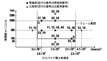
- the hydrogen concentration, mobility, threshold voltage, and flexibility of the protective insulating layer of the obtained semiconductor device were measured by the following methods, and the results are shown in Table 3.
- the hydrogen concentration of the protective insulating layer 20 provided on the substrate 10 was measured as follows.
- the obtained oxide semiconductor thin film transistor was put into a D-SIMS apparatus (AMETEK, IMS-6f), the inside of the chamber was evacuated to a high vacuum, and then the primary ion was formed in the region provided with the active layer made of the oxide semiconductor.
- the sample was set so as to be irradiated. While digging a sample by sputtering, mass analysis of secondary ions was performed. Cesium ions were used as primary ions. A profile in the depth direction of the elements composing the sample was obtained. The position of the protective insulating layer was identified from the profile of the constituent elements, and the average amount of hydrogen atoms detected in the entire protective insulating layer was defined as the hydrogen concentration of the protective insulating layer.
- the hydrogen concentration obtained by measuring a standard substrate in which the amount of doped hydrogen is known in advance under exactly the same conditions as the sample is used.
- the hydrogen concentration in the protective insulating layer was calibrated.
- the standard substrate is made of the same material as the protective insulating layer.
- the protective insulating film is mainly composed of silicon nitride (SiN)
- SiN substrate is used as the standard substrate.
- the protective insulating film is mainly composed of silicon oxide (SiO 2 )
- the standard substrate is composed of SiO 2.
- a substrate is used.
- the voltage between the drain and gate electrodes is fixed at 10 V
- the voltage between the gate and source electrodes is manipulated from ⁇ 10 V to 15 V
- the current flowing between the drain and gate electrodes is Measured (FIG. 5).
- the measurement was performed using a semiconductor parameter analyzer 4156C (manufactured by Agilent Technologies) at room temperature in a dark room. Based on this measurement result, the mobility of the oxide semiconductor thin film transistor was calculated. In this measurement region, the oxide semiconductor thin film transistor is in the saturation region, and thus the mobility was calculated using the following equation.
- Mobility ⁇ [2L / (W * Cox)] ⁇ ( ⁇ Id / ⁇ Vg) 1/2 (L: channel length of oxide semiconductor thin film transistor, W: channel width of oxide semiconductor thin film transistor, Cox: capacitance per unit area of gate insulating film, Id: drain-gate current, Vg: gate-source voltage ) Evaluation was given as follows according to the obtained mobility value.
- V on the threshold voltage of the oxide semiconductor thin film transistor
- evaluation was performed based on the following criteria. When the threshold voltage falls within the range of evaluation A, the driving voltage of the thin film transistor can be lowered, and the current when off (for example, the gate voltage is 0 V) can be reduced.
- the obtained oxide semiconductor thin film transistor was continuously bent 10 times so as to have a curvature radius of 100 mm, and then the mobility of the oxide semiconductor thin film transistor was measured. The obtained mobility was compared with the mobility before bending, and evaluation was given as follows.
- Example 2 A semiconductor device in the same manner as in Example 1 except that the base material A in Example 1 was changed to the base material B (the substrate B was degassed and the substrate provided with the protective insulating layer was referred to as the substrate B). Were manufactured and evaluated.
- Example 3 A semiconductor device was manufactured and evaluated in the same manner as in Example 1 except that the film formation condition 1-1 of the protective insulating layer in Example 1 was changed to the film formation condition 1-2.
- Example 4 A semiconductor device was manufactured and evaluated in the same manner as in Example 3 except that the base material A in Example 3 was changed to the base material B.
- Example 5 A semiconductor device was manufactured and evaluated in the same manner as in Example 1 except that the film forming condition 1-1 of the protective insulating layer in Example 1 was changed to the film forming condition 1-3.
- Example 6 A semiconductor device was manufactured and evaluated in the same manner as in Example 5 except that the base material A in Example 5 was changed to the base material B.
- Example 1 The semiconductor is the same as in Example 1 except that the porous layer and the protective insulating layer obtained by replacing the base material A of Example 1 with a glass substrate are not provided, and that the bonding with the support is not performed. A device was manufactured and evaluated.
- Example 1 A semiconductor device was manufactured and evaluated in the same manner as in Example 1 except that the film formation condition 1-1 of the protective insulating layer in Example 1 was changed to the film formation condition 1-S in Table 2 below. It was. Note that in the method of film formation condition 1-S, the annealing treatment after the formation of the protective insulating layer is not performed.
- Example 2 A semiconductor device was manufactured and evaluated in the same manner as in Example 1 except that the film formation condition 1-1 of the protective insulating layer in Example 1 was changed to the film formation condition 1-4 in Table 1.
- Comparative Example 3 A semiconductor device was manufactured and evaluated in the same manner as in Comparative Example 2 except that the base material A in Comparative Example 2 was replaced with the base material B.
- Example 4 A semiconductor device was manufactured and evaluated in the same manner as in Example 1 except that the film formation condition 1-1 of the protective insulating layer in Example 1 was changed to the film formation condition 1-5 in Table 1.
- Comparative Example 5 A semiconductor device was manufactured and evaluated in the same manner as in Comparative Example 4 except that the base material A in Comparative Example 4 was replaced with the base material B.
- Examples 1 to 6 and Comparative Examples 1 to 5 are semiconductor devices manufactured by using silicon nitride as the material for the protective insulating layer and adjusting the hydrogen concentration.
- Reference Example 1 is a semiconductor device using a glass substrate as a substrate. Table 3 shows the main points of the configuration and the evaluation results.
- the semiconductor devices of Examples 1 to 6 of the present invention have high mobility, a threshold voltage of a predetermined value, and excellent flexibility.
- the semiconductor device of Comparative Example 1 since the hydrogen concentration of the protective insulating layer formed by RF sputtering is too low, the protective insulating layer cannot completely cover the porous layer, and gas is generated during the process. Oxide semiconductor thin film transistors did not operate because they were generated or the substrate was damaged. Further, in the semiconductor devices of Comparative Example 2 and Comparative Example 3, although the protective insulating layer was formed by plasma CVD, since the hydrogen concentration of the protective insulating layer was reduced too much, the protective insulating layer was cracked, and the mobility was low. The transistor did not work after the bending test.
- Example 11 A semiconductor device was manufactured and evaluated in the same manner as in Example 1 except that the film formation condition 1-1 of the protective insulating layer in Example 1 was changed to the film formation condition 2-1 in Table 4 below. It was.
- the source gas TEOS means Tetra ethylene silane.
- the film forming temperature represents the temperature of the base material on which the protective insulating layer is being formed. Note that none of the film forming conditions 2-1 to 2-5 is subjected to annealing after the formation of the protective insulating layer.
- Example 12 A semiconductor device was manufactured and evaluated in the same manner as in Example 11 except that the base material A in Example 11 was changed to the base material B.
- Example 13 A semiconductor device was manufactured and evaluated in the same manner as in Example 11 except that the film formation condition 2-1 of the protective insulating layer in Example 11 was changed to the film formation condition 2-2.
- Example 14 A semiconductor device was manufactured and evaluated in the same manner as in Example 13 except that the base material A in Example 13 was changed to the base material B.
- Example 15 A semiconductor device was manufactured and evaluated in the same manner as in Example 11 except that the film formation condition 2-1 of the protective insulating layer in Example 11 was changed to the film formation condition 2-3.
- Example 16 A semiconductor device was manufactured and evaluated in the same manner as in Example 15 except that the base material A in Example 15 was changed to the base material B.
- Example 11 A semiconductor device was manufactured and evaluated in the same manner as in Example 11 except that the film formation condition 2-1 of the protective insulating layer in Example 11 was changed to the film formation condition 2-4.
- Comparative Example 12 A semiconductor device was manufactured and evaluated in the same manner as in Comparative Example 11 except that the base material A in Comparative Example 11 was replaced with the base material B.
- Example 13 A semiconductor device was manufactured and evaluated in the same manner as in Example 11 except that the film formation condition 2-1 of the protective insulating layer in Example 11 was changed to the film formation condition 2-5.
- Comparative Example 14 A semiconductor device was manufactured and evaluated in the same manner as in Comparative Example 13 except that the base material A in Comparative Example 13 was replaced with the base material B.
- Examples 11 to 16 and Comparative Examples 11 to 14 are semiconductor devices manufactured by using silicon oxide as a material for the protective insulating layer and adjusting the hydrogen concentration.
- Table 5 shows the main points of the configuration and the evaluation results.
- the semiconductor devices of Examples 11 to 16 of the present invention have high mobility, a threshold voltage in the vicinity of 0 V, and excellent flexibility.
- the protective insulating layer was formed by plasma CVD, the protective insulating layer was cracked by bending because the hydrogen concentration of the protective insulating layer was excessively lowered. The mobility after the test changed greatly.
- the threshold voltage deviated greatly from the vicinity of 0 V due to the adverse effect of hydrogen. From the results shown in Tables 4 and 5, it can be seen that the hydrogen concentration range that can solve the problem does not change even if the material of the protective insulating layer changes.
- Example 21 A semiconductor device was manufactured and evaluated in the same manner as in Example 1 except that the protective insulating layer thickness in Example 1 was changed from 400 nm to 100 nm.
- Example 22 A semiconductor device was manufactured and evaluated in the same manner as in Example 21 except that the base material A in Example 21 was changed to the base material B.
- Example 23 A semiconductor device was manufactured and evaluated in the same manner as in Example 1 except that the thickness of the protective insulating layer in Example 1 was changed from 400 nm to 2000 nm.
- Example 24 A semiconductor device was manufactured and evaluated in the same manner as in Example 23 except that the base material A in Example 23 was changed to the base material B.
- Example 25 A semiconductor device was manufactured and evaluated in the same manner as in Example 3 except that the thickness of the protective insulating layer in Example 3 was changed from 400 nm to 2000 nm.
- Example 26 A semiconductor device was manufactured and evaluated in the same manner as in Example 25 except that the base material A in Example 25 was changed to the base material B.
- Example 21 A semiconductor device was manufactured and evaluated in the same manner as in Example 1 except that the thickness of the protective insulating layer in Example 1 was changed from 400 nm to 80 nm.
- Comparative Example 22 A semiconductor device was manufactured and evaluated in the same manner as in Comparative Example 21 except that the base material A in Comparative Example 21 was changed to the base material B.
- Example 23 A semiconductor device was manufactured and evaluated in the same manner as in Example 1 except that the thickness of the protective insulating layer in Example 1 was changed from 400 nm to 2500 nm.
- Comparative Example 24 A semiconductor device was manufactured and evaluated in the same manner as in Comparative Example 23 except that the base material A in Comparative Example 23 was replaced with the base material B.
- Examples 21 to 26 and Comparative Examples 21 to 24 are semiconductor devices prepared by changing the thickness of the protective insulating layer made of silicon nitride. Table 6 shows the main points of the configuration and the evaluation results.
- the semiconductor devices of Examples 21 to 26 of the present invention have high mobility, a threshold voltage in the vicinity of 0 V, and excellent flexibility.
- the semiconductor devices of Comparative Example 21 and Comparative Example 22 since the protective insulating layer is too thin, the mobility of the oxide semiconductor thin film transistor is low due to the influence of the gas from the porous layer, and the threshold voltage is low. It is out of the predetermined value.
- the oxide semiconductor thin film transistors of Comparative Example 23 and Comparative Example 24 since the protective insulating layer is too thick, the protective insulating layer is cracked by the bending test, and the mobility before and after the bending test changes greatly. Was.
- Example 31 A semiconductor device was manufactured and evaluated in the same manner as in Example 11 except that the thickness of the protective insulating layer in Example 11 was changed from 400 nm to 100 nm.
- Example 32 A semiconductor device was manufactured and evaluated in the same manner as in Example 31 except that the base material A in Example 31 was changed to the base material B.
- Example 33 A semiconductor device was manufactured and evaluated in the same manner as in Example 11 except that the thickness of the protective insulating layer in Example 11 was changed from 400 nm to 2000 nm.
- Example 34 A semiconductor device was manufactured and evaluated in the same manner as in Example 33 except that the base material A in Example 33 was changed to the base material B.
- Example 35 A semiconductor device was manufactured and evaluated in the same manner as in Example 15 except that the thickness of the protective insulating layer in Example 15 was changed from 400 nm to 100 nm.
- Example 36 A semiconductor device was manufactured and evaluated in the same manner as in Example 35 except that the base material A in Example 35 was changed to the base material B.
- Example 37 A semiconductor device was manufactured and evaluated in the same manner as in Example 13 except that the thickness of the protective insulating layer in Example 13 was changed from 400 nm to 2000 nm.
- Example 38 A semiconductor device was manufactured and evaluated in the same manner as in Example 37 except that the base material A in Example 37 was changed to the base material B.
- Example 31 A semiconductor device was manufactured and evaluated in the same manner as in Example 11 except that the thickness of the protective insulating layer in Example 11 was changed from 400 nm to 80 nm.
- Comparative Example 32 A semiconductor device was manufactured and evaluated in the same manner as in Comparative Example 31 except that the base material A in Comparative Example 31 was replaced with the base material B.
- Example 33 A semiconductor device was manufactured and evaluated in the same manner as in Example 11 except that the thickness of the protective insulating layer in Example 11 was changed from 400 nm to 2500 nm.
- Comparative Example 34 A semiconductor device was manufactured and evaluated in the same manner as in Comparative Example 33 except that the base material A in Comparative Example 33 was replaced with the base material B.
- Examples 31 to 38 and Comparative Examples 31 to 34 are semiconductor devices created by changing the thickness of the protective insulating layer made of silicon oxide. Table 7 shows the main points of the configuration and the evaluation results.
- the semiconductor devices of Examples 31 to 38 of the present invention have high mobility, a threshold voltage in the vicinity of 0 V, and excellent flexibility.
- the oxide semiconductor thin film transistor did not operate due to the influence of the gas from the porous layer because the protective insulating layer was too thin.
- the protective insulating layer was too thick, the protective insulating layer was cracked by the bending test, and the mobility before and after the bending test was greatly changed. From the results of Tables 6 and 7, it can be seen that there is no difference in the film thickness range that can solve the problem even if the material of the protective insulating layer changes.
- Example 41 A semiconductor device was manufactured and evaluated in the same manner as in Example 1 except that the active layer of Example 1 was changed from InGaZnO to InZnO.
- Example 42 A semiconductor device was manufactured and evaluated in the same manner as in Example 41 except that the base material A in Example 41 was changed to the base material B.
- Example 43 A semiconductor device was manufactured and evaluated in the same manner as in Example 11 except that the active layer of Example 11 was changed from InGaZnO to InZnO.
- Example 44 A semiconductor device was manufactured and evaluated in the same manner as in Example 43 except that the base material A in Example 43 was changed to the base material B.
- Examples 41 to 44 are semiconductor devices manufactured by changing the material of an oxide semiconductor layer of an oxide semiconductor thin film transistor from InGaZnO to InZnO.
- Table 8 shows the main points of the configuration and the evaluation results.
- the semiconductor devices of Examples 41 to 44 of the present invention have high mobility, the threshold voltage is in the vicinity of 0 V, and are excellent in flexibility. From the comparison of the results in Tables 6 and 7 and Tables 6 and 8, it can be seen that the present invention can solve the problem even if the material of the oxide semiconductor is changed.
- FIG. 6 and FIG. 7 plots data of an example and a comparative example in which the material of the protective insulating layer is silicon nitride
- FIG. 7 plots data of an example and a comparative example using silicon oxide.
- the point ⁇ represents the example, and the point ⁇ represents the comparative example.
- the numbers written beside each point indicate the example or comparative example number.
- region enclosed with the square in each figure is an area
- the vicinity of B is a region where the protective insulating layer is thin and the hydrogen concentration in the protective insulating layer is the highest, so the threshold voltage is expected to be largely deviated from 0V. From the example, it can be seen that the threshold voltage is in a predetermined range. Moreover, it can be seen from the comparison between FIGS. 6 and 7 that the effective range does not change even if the material of the protective insulating layer is changed.
Landscapes
- Engineering & Computer Science (AREA)
- Microelectronics & Electronic Packaging (AREA)
- Power Engineering (AREA)
- Physics & Mathematics (AREA)
- Ceramic Engineering (AREA)
- Condensed Matter Physics & Semiconductors (AREA)
- General Physics & Mathematics (AREA)
- Computer Hardware Design (AREA)
- Thin Film Transistor (AREA)
Abstract
本発明は、移動度が高く、閾値電圧が所定の範囲にある酸化物半導体薄膜トランジスタ用基板及びそれを備えた可撓性の半導体装置を提供するものである。 本発明は、金属基部(11)と多孔質層(12)とを有する基材(10)を酸化物半導体薄膜トランジスタ用の基板として使用する場合に、この多孔質層上にシリコン化合物を主成分とし、かつ、水素を含む絶縁性を有する保護絶縁層(20)であって、水素濃度が3.5×10²¹atoms/cm3以上3.5×1022atoms/cm3以下であって、かつ、厚みが100nm以上2000nm以下の保護絶縁層(20)を形成するものである。この保護絶縁層(20)上に、活性層に酸化物半導体を含む薄膜トランジスタを設ける。
Description
本発明は、液晶、有機EL素子などを用いた表示装置、電子ペーパー、X線センサーなどの可撓性デバイスに使用できる酸化物半導体薄膜トランジスタに用いられる基板、半導体装置、およびその製造方法に関する。
特許文献1には、In-Ga-Zn-O系の酸化物半導体(InGaZnO)を活性層に用いた薄膜トランジスタ(TFT)が、比較的低温で成膜できて、樹脂基板の使用が可能となることから、フラットパネルディスプレイ(FPD)の薄型化、軽量化、可撓化に適した技術であることが記載されている。また、酸化物半導体薄膜トランジスタの活性層は、大気や、パターニングの際のエッチング液に暴露されると、酸化物半導体薄膜トランジスタの閾値電圧が0Vから大きく外れてしまうことが課題として挙げられ、活性層上に保護層を設けて保護することにより、課題を解決可能であることが開示されている。また、特許文献1には、樹脂基板だけでなく、表面を絶縁処理したアルミニウムなどの金属基板を用いてもよいことも記載されている。
特許文献2は、可撓性基板に関する特許文献であって、金属表面に陽極酸化処理によりポーラス(多孔質)構造を持つ酸化アルミニウム絶縁層を形成することにより、樹脂基板よりも耐熱性が高く、熱寸法安定性に優れ、かつショート等の故障を起さない可撓性基板が得られることが開示されている。
また、特許文献3は、樹脂製の可撓性基板に関する特許文献であって、樹脂基板を透過してくる透過ガスを低減するために、シリコン化合物を含有するガスバリア層を樹脂基板表面に設けることが提案されている。シリコン化合物に水素が10~30原子%含まれるように調節することにより、透過ガスをバリアするとともに、透明性と可撓性を両立できることが記載されている。
上記したように、特許文献1では、表面を絶縁処理した金属基板を用いてTFTを作製してもよいことが記載されている。しかしながら、かかる金属基板の具体例や、金属基板を用いて製造されたTFTの態様や具体例については説明がなされていない。
本出願人は、樹脂基板よりも耐熱性が高く、かつ、樹脂基板と比べ、ガスバリア性に問題が無い金属基板上に、酸化物半導体薄膜トランジスタを製造することを試みた。具体的には、特許文献2に記載の、多孔質アルミニウム陽極酸化絶縁膜を有する金属基板上に、特許文献1に記載された構成の酸化物半導体薄膜トランジスタを形成した。
しかし予想に反して、製造された酸化物半導体薄膜トランジスタは正常に動作しないことが分かった。具体的には、耐熱性が高く、ガスバリア性が高いと予想される金属基板を用いたにもかかわらず、酸化物半導体薄膜トランジスタの移動度、閾値電圧は所定の範囲にならなかった。一般に、閾値電圧は、ゼロボルト近傍でややマイナス寄りでありややマイナスにバイアス印加した状態でオフすることが好ましいとされている。
本発明は、上記の事情に鑑みてなされたものであり、移動度が高く、閾値電圧が所定の範囲にある酸化物半導体薄膜トランジスタを形成可能な可撓性酸化物半導体薄膜トランジスタ用基板および、それを用いて得られる可撓性半導体装置を提供するものである。
本発明者らは、多孔質陽極酸化絶縁膜を有するアルミニウム基板を真空装置に投入した際に真空引きに必要な時間が長いことなどから、陽極酸化アルミニウム基板表面の多孔質層にガスが吸着され、吸着したガスが製造中に放出されたり、製造後に拡散したりすることにより、InGaZnO-TFTの閾値電圧が0Vから大きく変化していると推測した。
そこで、特許文献3に記載のガスバリア層を設けた陽極酸化アルミニウム基板を準備し、その上に酸化物半導体薄膜トランジスタを形成して、酸化物半導体装置を作製した。しかし、特許文献3に記載のガスバリア層を設けても、依然として所望の特性を持つ半導体装置を得ることができなった。本出願人の詳細な検討の結果、陽極酸化アルミニウム基板の表面凹凸が大きいために、特許文献3に記載のガスバリア層では、基板の表面のカバレッジが十分ではなかったことが一つの原因であることがわかった。そこで、さらに基板の膜構成や製造方法を詳細に検討した結果、ついに上記の課題を解決し、本発明を完成するに至った。
上記目的を達成するために、本発明の可撓性酸化物半導体薄膜トランジスタ用基板は、金属基部の少なくとも一方の面上に形成された多孔質層を備えた基材と、前記多孔質層上に形成された、シリコン化合物を主成分とし、かつ、水素を含む保護絶縁層とを備えてなり、この保護絶縁層中の水素濃度が3.5×10²¹atoms/cm3以上3.5×1022atoms/cm3以下であって、かつ、保護絶縁層の厚みが100nm以上2000nm以下である。
本発明においては、シリコン化合物が窒化シリコン、酸化シリコン、酸窒化シリコンから選ばれる少なくとも1種であることが好ましい。
また、多孔質層はアルミニウムもしくはアルミニウム合金の陽極酸化膜とするのが好ましい。さらにまた、多孔質層は金属基部の両面に形成することが好ましい。
また、金属基部上に多孔質層が設けられこの多孔質層上に保護絶縁層が設けられた基板と、この保護絶縁層上に形成されたIn,Ga及びZnから選ばれる少なくとも1つの元素を含む酸化物半導体からなる活性層を備えた酸化物半導体薄膜トランジスタとを備えた、可撓性半導体装置とすることが好ましい。ここで、保護絶縁層は、少なくとも酸化物半導体からなる活性層が形成される領域の全域に設けられることが好ましい。さらに、酸化物半導体からなる活性層は、In,Ga,及びZnを含むことが好ましい。さらにまた、酸化物半導体からなる活性層がアモルファス性であることが好ましい。
酸化物半導体薄膜トランジスタは少なくとも、ゲート電極、ゲート絶縁膜、酸化物半導体からなる活性層、ソースおよびドレイン電極を有する。また、酸化物半導体薄膜トランジスタは基板上に形成され、少なくともゲート電極、ゲート絶縁膜、酸化物半導体からなる活性層、ソースおよびドレイン電極をこの順に有することが好ましい。さらにまた、前記酸化物半導体薄膜トランジスタのゲート絶縁膜が酸化シリコンを主成分とすることが好ましい。
本発明の可撓性半導体装置の製造方法は、金属基部上の少なくとも一表面に多孔質層を有する基材を準備し、前記多孔質層上の少なくとも一部に、シリコン化合物を主成分とし、水素濃度が3.5×10²¹atoms/cm3以上3.5×1022atoms/cm3以下であって、かつ、厚みが100nm以上2000nm以下である保護絶縁層をプラズマCVD(CVD:Chemical Vapor Deposition-化学気相成長)によって成膜し、該保護絶縁層の上にIn,Ga及びZnから選ばれる少なくとも1つの元素を含む酸化物半導体からなる活性層を有する酸化物半導体薄膜トランジスタを設けることを特徴とする。
本態様においては、保護絶縁層を成膜する前に、多孔質層を有する基材を大気より減圧下、かつ、350℃以上で加熱することが好ましい。
本発明においては、多孔質層上に設けられており、シリコン化合物を主成分とする層を保護絶縁層と呼ぶものとする。
本発明において、「主成分」とは、層を構成する材料の内、60質量%以上が指定の化合物からなることを意味する。
本発明において、「酸化物半導体薄膜トランジスタ」とは、少なくとも、ゲート電極、ゲート絶縁膜、酸化物半導体からなる活性層、ソース・ドレイン電極を有する薄膜トランジスタのことを意味する。
本発明において、「~の上に・・・」あるいは「~上に・・・」と記載した場合は、~の表面に直接に接して・・・を設けてある場合と、~の上に別の層が存在し、その層の上に・・・を設けた場合の両方を含むものとする。また、その場合、・・・は~の全域に設けられていてもよく、一部にのみ設けられていてもよい。
本発明の酸化物半導体薄膜トランジスタ用基板は、金属基部の表面に多孔質層を備え、更に、多孔質層上にシリコン化合物を主成分とし、かつ、水素を含む保護絶縁層とを備えてなり、保護絶縁層中の水素濃度が3.5×10²¹atoms/cm3以上3.5×1022atoms/cm3以下とし、保護絶縁層の厚みを100nm以上2000nm以下としている。本発明の酸化物半導体薄膜トランジスタ用基板を用いることにより、移動度が高く、閾値電圧が所定の範囲にある酸化物半導体薄膜トランジスタ及びそれを備えた可撓性の半導体装置を形成することができる。
以下に、添付の図面に基づいて、本発明の可撓性酸化物半導体薄膜トランジスタ用基板および可撓性半導体装置の実施形態を説明する。視認しやすくするために、図面の各部の縮尺は適宜変更して示してある。
図1は、可撓性半導体装置の実施態様を模式的に示す図である。
図1に示されるように、可撓性酸化物半導体薄膜トランジスタ用基板1aは、基材10と、基材10上に設けられた保護絶縁層20とからなる。また基材10は、金属基部11とその上に設けられた多孔質層12からなっている。多孔質層12は、金属基部11と上に設けられる保護絶縁層との間に位置し、表面の粗面化により上に設けられる層の密着を改善する働きを有する。
保護絶縁層20は、多孔質層12の表面に吸着されたガスが、製造プロセス中に製造装置内に放出されたり、製造後の拡散によって酸化物半導体層に悪影響を及ぼしたりすることを防止する役割を有する。また、保護絶縁層20は、製造プロセス中において、使用する酸やアルカリ等の薬品や、ドライエッチングおよびスパッタ成膜時のプラズマなどにより基材10がダメージを受けるのを防止する役割も有する。ここで、保護絶縁層20は、多孔質層12を被覆し、吸着ガス放出防止機能および製造プロセスダメージ防止機能を確保するために、シリコン化合物を主成分とし、水素濃度が3.5×10²¹atoms/cm3以上で、かつ100nm以上の膜厚を必要とする。また、基材10の可撓性を確保するため、および保護絶縁層20のクラックを防止するために、膜厚の上限は2000nmである。
また、酸化物半導体薄膜トランジスタの特性は、保護絶縁層20に含まれる水素量に影響を受ける。酸化物半導体薄膜トランジスタの閾値電圧を望ましい値にする為には保護絶縁層中の水素濃度が3.5×10²²atoms/cm3以下となるように形成される。
よって、保護絶縁層20は、水素濃度が3.5×10²¹atoms/cm3以上3.5×1022atoms/cm3以下の範囲に設定され、かつ、厚みが100nm以上2000nm以下に設定される。
図1においては、保護絶縁層20の上に、ゲート電極30、ゲート絶縁膜40、活性層50、エッチングストッパ層60およびソース・ドレイン電極70からなる酸化物半導体薄膜トランジスタ2が示してある。活性層50はIn,Ga及びZnから選ばれる少なくとも1つの元素を含む酸化物半導体からなる。ここで、特許文献1に示されるように、酸化物半導体薄膜トランジスタは、活性層が大気に暴露されると閾値電圧が0V近傍から大きく外れることが知られているが、図1の構成によれば、金属基部11を有する基材10によって、外部からの大気や水蒸気の侵入が低減され、保護絶縁層20により多孔質層12からのガス放出が低減され、保護絶縁層20自身も閾値電圧に悪影響を及ぼす水素成分が低減された構成とされているため、酸化物半導体薄膜トランジスタの閾値電圧が0V近傍となる。
以下に、基材、金属基部、多孔質層、保護絶縁層、酸化物半導体薄膜トランジスタについて順に説明する。
<基材>
基材10は、金属基部11と、該金属基部の少なくとも一表面上に形成された多孔質層12から構成される。金属基部11と多孔質層12からなる基材10は、可撓性とガスバリア性、プロセス耐性を有するので、酸化物半導体薄膜トランジスタ用の可撓性基板として、好適である。
基材10は、金属基部11と、該金属基部の少なくとも一表面上に形成された多孔質層12から構成される。金属基部11と多孔質層12からなる基材10は、可撓性とガスバリア性、プロセス耐性を有するので、酸化物半導体薄膜トランジスタ用の可撓性基板として、好適である。
基材10は、少なくとも金属基部11と多孔質層12を備えていれば好ましく使用することができるが、金属基部11をアルミニウム、ステンレスまたは鉄鋼板とアルミニウム薄板を一体化したクラッド材とすることで、アルミニウム薄板の陽極酸化処理が簡易となること、また、基材の耐久性が高くなることからより好ましい。さらに、鋼板の両面をアルミニウム薄板で挟んで一体化したクラッド材において、アルミニウム薄板表面を陽極酸化処理して得られた基材では、基材を構成する素材の熱膨張係数差に起因した基板の反り、及び膜剥がれ等を抑制することができるため、より好ましい。
多孔質層12を設けた基材10は、後に述べる保護絶縁層20を形成する前に減圧下で脱ガス処理を行うことが好ましい。脱ガス処理を実施することで、多孔質層に吸着されたガスの量を減らせるため、より好ましい。例えば、保護絶縁層を形成する成膜装置(例えばプラズマCVD装置)の前処理室にて、チャンバーを真空引きしながら350℃以上で多孔質層を設けた基材を加熱することで脱ガス処理が実施できる。保護絶縁層20を形成する成膜装置で脱ガス処理を行うことで、脱ガス処理後に大気に曝さずに保護絶縁層を設けられるため好ましい。また、前処理室にて処理することで、放出されたガスが、保護絶縁層成膜時に再度取り込まれる可能性を低くできるためより好ましい。この多孔質層の脱ガス処理は量産時の生産性の悪化を回避するため、できるだけ短い時間で脱ガス処理するのが好ましい。
次に、基材を構成する金属基部と、多孔質層について説明する。
<<金属基部>>
金属基部11は少なくとも一部が金属からなり、ガスバリア性を有する。また、薄板状にした金属基部を選択した場合には、ガスバリア性を維持しつつ可撓性を持たせることができ好ましい。
金属基部11は少なくとも一部が金属からなり、ガスバリア性を有する。また、薄板状にした金属基部を選択した場合には、ガスバリア性を維持しつつ可撓性を持たせることができ好ましい。
金属基部11の材質としては、アルミニウム(Al)、鉄(Fe)、ジルコニウム(Zr)、チタン(Ti)、マグネシウム(Mg)、銅(Cu)、ニオブ(Nb)およびタンタル(Ta)の中から選ばれる少なくとも1つの金属を含有する基板、あるいは上記金属の合金が好ましい。入手容易性、軽量性の観点からアルミニウムであることが好ましい。
金属基部11は単層であっても、複数層を積層したものであってもよく、素材が単体であっても合金であってもよい。たとえば熱膨張による伸縮や反りを調節する目的で、複数層の積層構成にしたり、合金を用いたりすることも可能である。金属基部の片面に多孔質層を設けた態様では、金属基部は多孔質層を除外した部分全てを指すものとする。また、金属基部の両面に多孔質層を設けた態様では、両面の多孔質に挟まれた領域全てを金属基部と呼ぶものとする。金属基部を複数層の構成とした場合には、少なくとも一層が金属からなる。
図2に、金属基部11が複数層から成る態様の一例を示した。図2では、金属基部11が3層構成からなる態様を示しており、補助基部11aが主要基部11bに挟まれた構成を記載している。例えば、補助基部11aと主要基部11bが一層ずつからなる積層構成としても好適である。複数層の構成とする場合には少なくとも一層が金属であればよく、もう一方の層は金属であっても、金属でなくてもよい。
金属基部に用いられる材質としては、例えば、ステンレス板や炭素繊維からなる板であってもよい。補助基部11aは、伸縮率の調整や、基材の補強、ガス透過率の低減などの目的で採用してもよい。補助基部11aとしては、金属薄板を用いるのが好ましく、ステンレス鋼材を用いるのが好ましい。
また、金属基部11の総厚み(複数層から成る場合はその和)は用途によって適宜選択可能であり、例えば、基板の強度と可撓性の観点から、5μm~200μmが好ましい。
<<多孔質層>>
図1に示されるように、金属基部11の上には多孔質層12が設けられる。
図1に示されるように、金属基部11の上には多孔質層12が設けられる。
多孔質層12は金属基部の表面の少なくとも一部分に設けられ、金属基部11の表面を絶縁化するとともに、アンカー効果によって、その上に設けられる層の密着性を改善できる。また、多孔質層12は、層自体の可撓性にも優れている。可撓性の観点では、多孔質層12の細孔の径は、約10nm前後であることが好ましい。
多孔質層12は金属基部の一方の面全体に設けるのが好ましく、金属基部の両面全体に設けるのがさらに好ましい。金属基部の両面に等しく多孔質層を設けた場合には、応力が均一となり、基板に反りが発生しにくくより好ましい。
図1、図2では、金属基部11と多孔質層12が直接に接している態様を示しているが、必要に応じて別の層を間に設けてもよい。例えば金属基部表面の絶縁性をさらに向上させるための絶縁層や、多孔質層を付設しやすくするための下地層を設けてもよい。
多孔質層12の素材としては、絶縁性の金属酸化物であるのが好ましく、金属基部11と同じ金属を含む酸化物であるのがさらに好ましい。多孔質層12はどんな製造方法で作られてもよく、絶縁性多孔質微粒子とバインダーを分散した液を金属基部11の表面に塗工して多孔質層としてもよく、金属基部11の表面部分を多孔質層化してもよい。中でも、金属基部11と多孔質層12との密着性、絶縁性(ピンホールが生じにくい)の観点から、金属基部の一部を陽極酸化処理することで多孔質層化した態様が好ましい。
また、多孔質層12の厚みは用途によって適宜選択可能であるが、絶縁性と密着性の観点から、0.1μm~100μmとすることが好ましく、0.5μm~50μmがさらに好ましく、5μm~20μmがもっとも好ましい。多孔質層12として、金属酸化物からなる層を設けた場合は、厚みを50μm以下とすることで、可撓性を確保しやすいため好ましい。また厚みを0.5μm以上とすることで、絶縁性が確保されやすいため好ましい。
<<<陽極酸化処理により得られる多孔質層>>>
陽極酸化処理による多孔質層の形成方法は特に限定されるものではなく、金属表面に陽極酸化多孔質層が形成できればどんな方法で行っても本発明の範疇である。以下に、陽極酸化によって形成された多孔質層について説明する。
陽極酸化処理による多孔質層の形成方法は特に限定されるものではなく、金属表面に陽極酸化多孔質層が形成できればどんな方法で行っても本発明の範疇である。以下に、陽極酸化によって形成された多孔質層について説明する。
従来から、陽極酸化を利用した多孔質層の製造方法は、ナノメートルオーダーの細孔を形成できる簡易な方法として知られている。また、この多孔質層は金属酸化物であるため、高い絶縁性を有することが知られている。具体的には、硫酸、シュウ酸、または燐酸等の酸性電解液またはアルカリ性電解液中に、金属基材を浸漬し、これを陽極として電流を流すと、金属基材の表面で酸化と溶解が同時に進行し、その表面に細孔を有する酸化膜を形成することができる。
陽極酸化を利用した多孔質層を形成するための金属としては、適宜選択可能であるが、例えば、アルミニウム(Al)、鉄(Fe)、ジルコニウム(Zr)、チタン(Ti)、マグネシウム(Mg)、銅(Cu)、ニオブ(Nb)およびタンタル(Ta)の中から選ばれる少なくとも1つの金属、あるいは上記金属の合金が好ましい。
図4に、陽極酸化処理により得られる多孔質層の模式図を示す。図4では、金属基部11の片面にのみ陽極酸化処理を施し、多孔質層12を設けた態様を示す。金属基部11の被処理面は一様に金属酸化物に変化するとともに、ナノメートルオーダーの細孔120が形成される。陽極酸化処理により被処理面が一様に処理されるため、高い絶縁性を確保できる。また、もともとの金属基部の表面を処理して形成した多孔質層であるため、金属基部11と多孔質層12は強く結合して容易に剥離しない。さらに、この多孔質層上に次の層(図示せず)を形成した場合には、成膜時に細孔120内にも次の層の成分が入り込むため、いわゆるアンカー効果により密着性が確保される。
次に陽極酸化処理の方法の一例を記載する。準備した金属、または合金からなる金属基部を水洗した後、金属用の脱脂剤で脱脂して表面に付着した汚れを落とし、水洗により脱脂剤を洗い流す。次に、5質量%~20質量%の硝酸水溶液で硝酸洗浄を行い、しかる後に、再び水洗を行う。次に、金属基部を硫酸浴中、あるいはシュウ酸浴中で所定の電流密度で陽極酸化処理し、金属基部の表面に、多孔質の陽極酸化皮膜を形成する。また、陽極酸化処理時に流す電流値は、金属種によって最適値が異なるが、電流値が小さすぎると金属の溶解が支配的になり、必要とする多孔質層が形成されない可能性がある。また、電流値が大きすぎると多孔質層が急激に成長するため、表面に一様で無い状態となったり、一部が剥がれやすくなったりする可能性がある。
<保護絶縁層>
図1に示されるように、多孔質層12の少なくとも一部の表面上には保護絶縁層20が設けられる。保護絶縁膜20は、多孔質層12の表面に吸着されたガスが、製造プロセス中に製造装置内に放出されたり、製造後の拡散によって酸化物半導体層に悪影響を及ぼしたりすることを防止する役割を有する。また、保護絶縁層20は製造プロセスで使用する酸やアルカリ等の薬品や、ドライエッチングおよびスパッタ成膜時のプラズマなどにより基材10がダメージを受けるのを防止する役割も有する。
図1に示されるように、多孔質層12の少なくとも一部の表面上には保護絶縁層20が設けられる。保護絶縁膜20は、多孔質層12の表面に吸着されたガスが、製造プロセス中に製造装置内に放出されたり、製造後の拡散によって酸化物半導体層に悪影響を及ぼしたりすることを防止する役割を有する。また、保護絶縁層20は製造プロセスで使用する酸やアルカリ等の薬品や、ドライエッチングおよびスパッタ成膜時のプラズマなどにより基材10がダメージを受けるのを防止する役割も有する。
図3に、保護絶縁層20が多孔質層12の一部に設けられた態様の断面模式図を示す。図3に一例を示すように、保護絶縁層20は、少なくとも酸化物半導体薄膜トランジスタ2の活性層50が形成された領域に設けることが好ましい。また、少なくとも酸化物半導体薄膜トランジスタ2の形成領域に設けることがより好ましく、多孔質層の全域を覆うように設けることがさらに好ましい。多孔質層の表面の一部のみを保護絶縁層で覆うことでも発明の効果は得られるが、多孔質層の表面全域を覆っておくことで製造プロセス中に多孔質層からガスが放出されて成膜装置を汚染したり、放出されたガスが活性層に取り込まれたりすることを防止できるため好ましい。また、酸化物半導体薄膜トランジスタを製造するプロセス中に、基材10がプラズマ、酸・アルカリの薬品や有機溶剤に暴露されて受けるダメージが、保護絶縁層により低減されるためより好ましい。
図1~図3においては、保護絶縁層20と基材10は直接に接するように記載されているが、この間に別の層を有していてもよい。例えば多孔質層の凹凸を低減するための平坦化層や、多孔質層と保護絶縁層の密着を改善するための下地層を設けてもよい。
保護絶縁層20は、シリコン化合物を主成分とし、かつ、水素を含む層である。シリコン化合物としてはどんなシリコン化合物であってもよいが、酸化物半導体薄膜トランジスタ2の製造プロセス中に、基材10がダメージを受けるのを防止できるという点で、酸化シリコン、窒化シリコン、酸窒化シリコンとするのが好ましい。このようなシリコン化合物は、スパッタやCVDにより成膜した場合には、水素が膜中に取り込まれることが知られている。
本出願人らの様々な検討により、上記の保護絶縁層が、シリコン化合物を主成分とし、水素濃度が3.5×10²¹atoms/cm3以上でかつ膜厚が100nm以上とすることで保護絶縁層として機能することがわかった。保護絶縁層としての機能とは、(1)多孔質層12の表面に吸着されたガスが、製造プロセス中に製造装置内に放出されたり、製造後の拡散によって酸化物半導体層に悪影響を及ぼしたりすることを防止する機能、(2)保護絶縁層20は製造プロセス中に製造プロセスで使用させる酸やアルカリなどの薬品やドライエッチングおよびスパッタ成膜時のプラズマなどにより基材10がダメージを受けるのを防止する機能、(3)可撓性、の3つである。
基材10は多孔質層を有しており、そのために表面の凹凸が激しい。保護絶縁層として機能する為には、多孔質層を被覆する必要があるが、保護絶縁層の水素濃度が3.5×10²¹atoms/cm3未満になると、膜が緻密になり硬くなるため、クラックが発生したり、またカバレッジ性に劣ったりするため、多孔質層を良好に被覆することが難しい。また水素濃度が3.5×1021atoms/cm3以上の場合でも、表面の凹凸が激しい多孔質層を被覆するには膜厚が100nm必要であることも明らかにした。
さらに本出願人らは、保護絶縁層に含まれる水素が拡散して、酸化物半導体薄膜トランジスタの活性層に入り込み、活性層中のキャリヤ量を増加させて酸化物半導体薄膜トランジスタの移動度、閾値電圧に影響を及ぼすことを解明した。保護絶縁層を詳細に検討した結果、保護絶縁層の水素濃度を3.5×10²²atoms/cm3以下とすることで酸化物半導体薄膜トランジスタの閾値電圧を所定の範囲に制御できることがわかった。
結果として、基材10上に設ける保護絶縁層の水素濃度は3.5×10²¹atoms/cm3以上3.5×1022atoms/cm3以下とすべきことが判明した。なお、ここで、「atoms/cm3」は1cm3あたりに含まれる原子の個数を意味する。
また、たとえ上記の水素濃度範囲および膜厚となるように保護絶縁層20を設けたとしても、膜厚が厚すぎる場合は、半導体装置3を屈曲させた際に保護絶縁層20にクラックが入りやすくなったり、保護絶縁層20の膜剥がれを生じたりして、ガスが侵入して酸化物半導体薄膜トランジスタ2の移動度劣化等の特性悪化を生じてしまう。本発明者らによる検討の結果、水素濃度の調節に加え、100nm以上2000nm以下の厚みを有する保護絶縁層とすることが課題の解決に重要であることも判明した。
保護絶縁層は、シリコン化合物を主成分とする層であり、単層であっても複数のシリコン化合物の層から成っていてもよい。保護絶縁層が複数層から成る場合には、複数層の合計膜厚が100nm~2000nmの範囲となるようにする。また、複数層を設ける場合は、複数の保護絶縁層の内、少なくとも酸化物半導体薄膜トランジスタが設けられる側に最も近い保護絶縁層の水素濃度を、3.5×10²¹atoms/cm3以上3.5×1022atoms/cm3以下とする。
保護絶縁層の水素濃度の測定は、二次イオン質量分析法(SIMS:Secondary Ion Mass Spectroscopy)により行うことができる。SIMSは対象物を構成する元素を非常に高感度で検出することができる分析法として知られており、分析対象物にビーム状のイオン(一次イオン)を衝突させ、衝突により対象物を構成する物質をイオン化(二次イオン)させる。この二次イオンを質量分析することで構成元素とその量を検出するものである。
SIMSの中でもダイナミックSIMS(D-SIMS:Dynamic-SIMS)と呼ばれる測定方法により保護絶縁層の水素濃度が測定できる。D-SIMSでは、セシウムイオンや酸素イオン(一次イオン)をサンプルに衝突させて、構成元素の二次イオンを発生させ、対象物を深さ方向に掘り進めながら分析を行うことができる。測定結果は、構成元素の深さ方向のプロファイルとして得られ、元素濃度の絶対値は、あらかじめ元素含有量が判明している標準基板の測定結果のプロファイルを参照することで求めることができる。水素濃度を測定するために、衝突させる一次イオンとしては、セシウムイオンを使用する。また、検出感度が非常に高いため、測定は超高真空下(1.0×10⁻⁵Pa以下)で行う。
保護絶縁層20は、どんな方法により形成されてもよいが、水素濃度を3.5×10²¹atoms/cm3以上3.5×1022atoms/cm3以下の範囲に調節しやすく、500℃以下の低温で良質な絶縁膜を、比較的高い成膜レートを実現できる点からプラズマCVD(別名PE-CVD、Plasma Enhanced-CVD)により形成されるのが好ましい。プラズマCVDでは、反応ガスをプラズマ状態にして活性なラジカルやイオンを生成させ,活性環境下で化学反応を行わせて所望の膜を被着体上に形成する。プラズマCVDとしては、200℃以下の低温でも所望の保護絶縁層を成膜することができるので、容量結合プラズマCVD(CCP-CVD:Capacitive Coupled Plasma-CVD)が特に好ましい。
保護絶縁層20の水素濃度は、成膜中に導入する原料ガスの流量や、保護絶縁層を成膜中の基板の温度、また、成膜後のアニール温度によって調節することができる。例えば窒化シリコンを保護絶縁層として用いる場合には原料ガスとしてSiH4とNH3とH2ガスを用いるが、H2の流量を調節しながら膜を形成することで、保護絶縁層中の水素濃度を調節することができる。また、上記の複数の調節方法を併用して水素濃度を調節してもよい。水素濃度再現性の観点から、基板温度による水素濃度調節、H2ガス流量による水素濃度調節が好ましい。
保護絶縁層の上に、後述の酸化物半導体薄膜トランジスタを直接設置する場合には、保護絶縁層は電気絶縁性である。電気絶縁性とは、保護絶縁層のシート抵抗値が1.0×10⁷Ω/□以上であることを指す。1.0×109Ω/□以上であればより好ましい。前記のシート抵抗値とすることで、酸化物半導体薄膜トランジスタの素子間のリークやショートなどを引き起こさないため好ましい。
また、図1では保護絶縁層20の上に直接酸化物半導体薄膜トランジスタ2を設けた態様を示しているが、保護絶縁層20と酸化物半導体薄膜トランジスタ2の間に、別の層を設けていてもよい。例えば、基板の平坦性を良くする平坦化膜、絶縁性をさらに改善する絶縁層や、酸化物半導体薄膜トランジスタ2と保護絶縁層の密着を改善する下地層を設けてもよい。この場合には、平坦化膜、絶縁層や下地層においても酸化物半導体薄膜トランジスタ2に悪影響を及ぼさないように、水素濃度を調節することが好ましい。
<半導体装置>
半導体装置とは、基板上に、少なくともゲート電極、ゲート絶縁膜、酸化物半導体からなる活性層、ソース・ドレイン電極、からなる酸化物半導体薄膜トランジスタを備えた装置のことを指す。
半導体装置とは、基板上に、少なくともゲート電極、ゲート絶縁膜、酸化物半導体からなる活性層、ソース・ドレイン電極、からなる酸化物半導体薄膜トランジスタを備えた装置のことを指す。
酸化物半導体薄膜トランジスタは、成膜温度が低いことから可撓性基板上に形成しやすく、これを用いた表示装置等の薄型化、軽量化、可撓化に貢献する技術である。一方で、このような酸化物半導体を用いた装置は外界から不純物が少量でも混入すると、酸化物半導体内でキャリヤが発生してしまうため、従来のシリコンを活性層として用いた薄膜トランジスタよりも基材や隣接層の不純物含有量が重要となる。
図1に示す酸化物半導体薄膜トランジスタ2は、ゲート電極30、ゲート絶縁膜40、活性層50、エッチングストッパ層60、ソース・ドレイン電極70からなる。図1ではボトムゲートタイプの酸化物半導体薄膜トランジスタを記載したが、トップゲートタイプであっても、ゲート電極が複数あるタイプであっても本発明の範疇である。図1にはエッチングストッパ層60を記載したが、特に必要ない場合は設けない構成でも本発明の範疇である。また、その他の構成についても本発明の範囲で変更が可能である。以降に、酸化物半導体薄膜トランジスタを構成する各部(活性層、エッチングストッパ層、ゲート電極、ゲート絶縁膜、ソース・ドレイン電極)について、図1に基づいて説明する。
<<活性層>>
活性層50は、酸化物半導体からなる。酸化物半導体は成膜温度が比較的低く、高温の結晶化工程が無くとも高い移動度を有するため、精力的に研究開発が進められている。活性層50の素材としては、In、Ga及びZnから選ばれる少なくとも1つの元素を含む酸化物半導体を用いる。中でも、In、Ga及びZnを含む酸化物半導体(InGaZnO)を用いると、高い移動度が得られるため好ましい。
活性層50は、酸化物半導体からなる。酸化物半導体は成膜温度が比較的低く、高温の結晶化工程が無くとも高い移動度を有するため、精力的に研究開発が進められている。活性層50の素材としては、In、Ga及びZnから選ばれる少なくとも1つの元素を含む酸化物半導体を用いる。中でも、In、Ga及びZnを含む酸化物半導体(InGaZnO)を用いると、高い移動度が得られるため好ましい。
酸化物半導体であればその組成に依存せず、水素の混入によりキャリヤが発生するため、閾値電圧が0V近傍から大きく外れるという課題が生じる。よって、発明の効果は、金属基部と多孔質層とを有する基板を採用し、酸化物半導体を活性層に用いた酸化物半導体薄膜トランジスタを備えた装置において発揮されうる。
活性層50は、ゲート電極30に電圧を印加した際にキャリヤを発生する層として機能するものである。活性層50を構成する酸化物半導体としては、例えば、In2O3、ZnO、Indium-Zinc-Oxide(InZnO)、Gallium-Zinc-Oxide(GaZnO)、Indium-Gallium-Oxide(InGaO)、Indium-Gallium-Zinc-Oxide(InGaZnO)が用いられる。高い移動度および低オフ電流が得られる点でInGaZnOが好ましい。
活性層50は、酸化物半導体のうち、耐熱性が低い基板に形成することができるアモルファス酸化物半導体により構成されることが好ましい。また、基板等の耐熱性に心配が無い場合には結晶性の酸化物半導体を選択することも可能である。低温で作製可能な良好なアモルファス酸化物半導体としては、少なくともIn、GaあるいはZnを含むアモルファス酸化物半導体であることが好ましい。活性層50に用いられるアモルファス酸化物半導体としては、In、Ga及びZnを含む酸化物として構成され、結晶状態における組成がInGaO3(ZnO)m(mは5以下の自然数)で表されるアモルファス酸化物半導体が好ましく、特に、InGaZnO4で表されるアモルファス酸化物半導体がより好ましい。この組成のアモルファス酸化物半導体の特徴としては、電気伝導度が増加するにつれ、電子移動度が増加する傾向を示す。また、電気伝導度を制御するには、成膜中の酸素分圧の調整により制御が可能である。酸化物半導体がアモルファスであるかどうかは、エックス線回折測定により確認できる。エックス線回折測定を行い、回折ピークが見られなければアモルファスである。
なお、活性層50は、その厚さが、1nm~200nmであることが好ましく、より好ましくは2.5nm~100nmである。
活性層50の製造方法は、特に限定されるものではない。例えば、印刷方式、コ-ティング方式等の湿式方式、真空蒸着法、スパッタ法、イオンプレ-ティング法等の物理的方式、CVD、プラズマCVD法等の化学的方式等を用いて形成される。これらの中から、活性層50を構成する材料との適性を考慮して適宜形成方法が選択される。例えば、InとGaとZnを含む酸化物半導体を活性層として用いる場合には、低温でも良質な膜質の成膜が可能であるとの観点から、スパッタ法により成膜されるのが好ましい。
これらの酸化物半導体、特にアモルファス酸化物半導体を活性層に用いた酸化物半導体薄膜トランジスタは、表面の凹凸が激しい基板上に作製した場合にも高い移動度が得られる。よって、本発明の基板上に設ける薄膜トランジスタとして適している。逆にSiを活性層に用いた薄膜トランジスタおよび有機半導体を活性層に用いた薄膜トランジスタは、基板の表面形状に敏感であって、基板表面がフラットでないと所望の特性が得られない。よって、表面の凹凸が比較的大きい本発明の基板上に設けるトランジスタとしては、不適である。
<<エッチングストッパ層>>
図1において、エッチングストッパ層60は、活性層50、特にチャネル領域Cが、ソース・ドレイン電極70のパターン時にエッチングされないように保護するエッチングストッパとして機能するものである。また、エッチングストッパ層は、外界から活性層に不純物が混入することを防ぐ役割も果たす。このエッチングストッパ層60は、少なくとも活性層50のチャネル領域Cを覆うように設けられることが好ましい。また、エッチングストッパ層はシリコンあるいはガリウムの酸化物により構成されることが好ましい。例えば、酸化シリコン、酸化ガリウム、窒化シリコン、酸窒化シリコンや酸化チタンが好ましく用いられる。
図1において、エッチングストッパ層60は、活性層50、特にチャネル領域Cが、ソース・ドレイン電極70のパターン時にエッチングされないように保護するエッチングストッパとして機能するものである。また、エッチングストッパ層は、外界から活性層に不純物が混入することを防ぐ役割も果たす。このエッチングストッパ層60は、少なくとも活性層50のチャネル領域Cを覆うように設けられることが好ましい。また、エッチングストッパ層はシリコンあるいはガリウムの酸化物により構成されることが好ましい。例えば、酸化シリコン、酸化ガリウム、窒化シリコン、酸窒化シリコンや酸化チタンが好ましく用いられる。
エッチングストッパ層60は、厚さ10nm~300nmであることが好ましく、より好ましくは50nm~150nmである。また、エッチングストッパ層60の製造方法としては、特に限定されないが、印刷方式、コ-ティング方式等の湿式方式、真空蒸着法、スパッタ法、イオンプレ-ティング法等の物理的方式、CVD、プラズマCVD法等の化学的方式等を用いて形成される。これらの中から、エッチングストッパ層60を構成する材料との適性を考慮して適宜形成方法が選択される。例えば、酸化シリコンをエッチングストッパ層60として用いる場合には、プラズマCVD法が好適に用いられる。
<<ゲート電極>>
ゲート電極30は、例えば、Al、Mo、Cr、Ta、Ti、Au、またはAg等の金属もしくはそれらの合金、Al-Nd、APC等の合金、酸化錫、酸化亜鉛、酸化インジウム、酸化インジウム錫(ITO)、酸化インジウム亜鉛(InZnO)等の金属酸化物導電物質、ポリアニリン、ポリチオフェン、ポリピロ-ル等の有機導電性化合物、またはこれらの混合物を用いて形成される。ゲート電極30としては、Mo、Mo合金(Mo-5at%Nbなど)またはCrを用いることが好ましい。このゲート電極30の厚さは、例えば、10nm~1000nmである。また、より好ましくは、20nm~500nmであり、さらに好ましくは40nm~100nmである。
ゲート電極30は、例えば、Al、Mo、Cr、Ta、Ti、Au、またはAg等の金属もしくはそれらの合金、Al-Nd、APC等の合金、酸化錫、酸化亜鉛、酸化インジウム、酸化インジウム錫(ITO)、酸化インジウム亜鉛(InZnO)等の金属酸化物導電物質、ポリアニリン、ポリチオフェン、ポリピロ-ル等の有機導電性化合物、またはこれらの混合物を用いて形成される。ゲート電極30としては、Mo、Mo合金(Mo-5at%Nbなど)またはCrを用いることが好ましい。このゲート電極30の厚さは、例えば、10nm~1000nmである。また、より好ましくは、20nm~500nmであり、さらに好ましくは40nm~100nmである。
ゲート電極30の形成方法は、特に限定されるものではない。例えば、印刷方式、コ-ティング方式等の湿式方式、真空蒸着法、スパッタ法、イオンプレ-ティング法等の物理的方式、CVD、プラズマCVD法等の化学的方式等を用いて形成される。これらの中から、ゲート電極30を構成する材料との適性を考慮して適宜形成方法が選択される。例えば、MoまたはMo合金を用いてゲート電極30を形成する場合、DCスパッタ法が用いられるのが好ましい。
<<ゲート絶縁膜>>
ゲート絶縁膜40にはSiO2、SiNx、SiON、Al2O3、YsO3、Ta2O5、もしくはHfO2等の絶縁体、またはそれらの化合物を少なくとも二つ以上含む混晶化合物が用いられる。ゲート絶縁膜としては、絶縁性の観点からSiO2が最も好ましく用いられる。酸化物半導体薄膜トランジスタにおいて、ゲート絶縁膜にSiO2を用いることにより、高移動度かつ低オフ電流を両立した、優れた半導体装置が実現できるので、好ましい。
ゲート絶縁膜40にはSiO2、SiNx、SiON、Al2O3、YsO3、Ta2O5、もしくはHfO2等の絶縁体、またはそれらの化合物を少なくとも二つ以上含む混晶化合物が用いられる。ゲート絶縁膜としては、絶縁性の観点からSiO2が最も好ましく用いられる。酸化物半導体薄膜トランジスタにおいて、ゲート絶縁膜にSiO2を用いることにより、高移動度かつ低オフ電流を両立した、優れた半導体装置が実現できるので、好ましい。
ゲート絶縁膜40の厚さは、10nm~10μmが好ましい。ゲート絶縁膜40は、リーク電流を減らすため、電圧耐性を上げるために、ある程度膜厚を厚くする必要がある。しかしながら、ゲート絶縁膜40の膜厚を厚くすると、酸化物半導体薄膜トランジスタの駆動電圧の上昇を招く。このため、ゲート絶縁膜40の厚さは、50nm~1000nmであることがより好ましい。また、より好ましくは、100nm~500nmである。
なお、HfO2のような高誘電率絶縁体をゲート絶縁膜40に用いることができる。高誘電率絶縁体を用いると、低電圧での酸化物半導体薄膜トランジスタの駆動が可能である。
ゲート絶縁膜40の形成方法は、特に限定されるものではない。例えば、印刷方式、コ-ティング方式等の湿式方式、真空蒸着法、スパッタ法、イオンプレ-ティング法等の物理的方式、CVD、プラズマCVD法等の化学的方式等を用いて形成される。
<<ソース・ドレイン電極>>
ソース電極・ドレイン電極70は、例えば、Al、Mo、Cr、Ta、Ti、Au、またはAg等の金属もしくはこれらの合金、Al-Nd、APC等の合金、酸化錫、酸化亜鉛、酸化インジウム、酸化インジウム錫(ITO)、酸化インジウム亜鉛(InZnO)等の金属酸化物導電物質を用いて形成される。なお、ITOについては、アモルファスITOでも、結晶化ITOでもよい。
ソース電極・ドレイン電極70は、例えば、Al、Mo、Cr、Ta、Ti、Au、またはAg等の金属もしくはこれらの合金、Al-Nd、APC等の合金、酸化錫、酸化亜鉛、酸化インジウム、酸化インジウム錫(ITO)、酸化インジウム亜鉛(InZnO)等の金属酸化物導電物質を用いて形成される。なお、ITOについては、アモルファスITOでも、結晶化ITOでもよい。
ソース電極・ドレイン電極70としては、MoまたはMo合金を用いることが好ましい。なお、ソース電極・ドレイン電極70の厚さは、例えば、10nm~1000nmである。特に好ましい範囲は50nm~400nmである。
なお、ソース電極・ドレイン電極70の形成方法は特に限定されるものではない。上述の組成の導電膜は、例えば、印刷方式、コ-ティング方式等の湿式方式、真空蒸着法、スパッタ法、イオンプレ-ティング法等の物理的方式、CVD、プラズマCVD法等の化学的方式等を用いて形成される。
例えば、ソース電極・ドレイン電極70を、MoもしくはMo合金、アモルファスITOで形成する場合、フォトリソグラフィー法を用いてMo膜もしくはMo合金膜またはアモルファスITO膜にレジストパターンを形成し、酸のエッチング液により、Mo膜もしくはMo合金膜またはアモルファスITO膜をエッチングしてソース電極・ドレイン電極70を形成する。
<<保護膜ならびその他の層>>
図1には、図示されていないが、酸化物半導体薄膜トランジスタ2上には必要に応じて保護膜が形成される。保護膜は酸化シリコン、窒化シリコン等の無機膜でもよいし、アクリル樹脂、ポリイミド樹脂などの有機膜でもよく、無機膜/有機膜の積層構造でもよい。
図1には、図示されていないが、酸化物半導体薄膜トランジスタ2上には必要に応じて保護膜が形成される。保護膜は酸化シリコン、窒化シリコン等の無機膜でもよいし、アクリル樹脂、ポリイミド樹脂などの有機膜でもよく、無機膜/有機膜の積層構造でもよい。
また、酸化物半導体薄膜トランジスタを表示装置に応用する場合は、画素電極が設けられて、それらは酸化物半導体薄膜トランジスタのソース電極と電気的に接続される。
以上、本発明の可撓性酸化物半導体薄膜トランジスタ用基板、および、この基板を用いた半導体装置について好ましい実施形態を元に説明したが、本発明は上記実施形態に限定されるものではない。また、本発明の半導体装置は、液晶、EL素子などを用いた表示装置、電子ペーパー、X線センサーに使用できる。さらに、本実施形態の半導体装置を用いた表示装置は、携帯電話のディスプレイ、パーソナルデジタルアシスタント(PDA)、コンピュータディスプレイ、自動車の情報ディスプレイ、TV用モニターを含む、幅広い分野に応用可能である。
以下、本発明の半導体装置について、実施例を元に具体的に説明するが、本発明はこれに限定されるものではない。
本発明の実施例、比較例で使用する基材について説明する。
~基材Aの製造~
図1に示される構成の、基材10の製造方法を説明する。
市販の高純度アルミニウム(純度99.99%)を用い、圧延して、厚さが40μmのアルミニウム薄板を用意した。次に、この薄板の端面をマスキングフイルムで被覆した後、エタノールで超音波洗浄して、酢酸+過塩素酸溶液で電解研磨した。その後、80g/Lのシュウ酸水溶液中で40Vの定電圧電解を実施することにより、多孔質層(アルミニウムの陽極酸化膜)をアルミニウム薄板の両面に形成して基材Aを得た。得られた基材Aの断面TEMを測定したところ、図1の基材10の構成となっていた。断面TEM画像から各層の厚さを任意で5箇所測定して平均厚さを確認したところ、金属基部11の厚さは約20μm、多孔質層12の厚さは両面ともに約10μmであった。
断面TEM画像からで多孔質層12の平均細孔サイズを確認したところ、約10nmであった。
~基材Bの製造~
図2に示される構成の、基材10の製造方法を説明する。
図2に示される構成の、基材10の製造方法を説明する。
市販のフェライト系ステンレス鋼(SUS430)と市販の高純度アルミニウム(純度99.99%)とを用い、冷間圧延法によりアルミニウム/ステンレス鋼/アルミニウムの3層構成となるように積層した。得られた上記の積層体は、アルミニウム部分の厚さが30μm、ステンレス鋼の厚さが50μmの3層構成の金属薄板(総厚さ110μm)であった。次に、この薄板の端面をマスキングフイルムで被覆した後、エタノールで超音波洗浄して、酢酸+過塩素酸溶液で電解研磨した。その後、80g/Lのシュウ酸水溶液中で40Vの定電圧電解することにより、多孔質層(アルミニウムの陽極酸化膜)をアルミニウムの表面(2層あるアルミニウムの両方の表面)に形成して基材Bを得た。
得られた基材Bの断面TEMを測定したところ、図2の基材10の構成となっていた。断面TEM画像から各層の厚さを任意に5箇所測定して平均厚みを確認したところ、補助基部11a(ステンレス鋼からなる)の厚さが50μm、主要基部11b(アルミニウムからなる)の厚さがどちらも20μm、多孔質層12の厚さが両面ともに約10μmであった。
断面TEM画像から多孔質層12の平均細孔サイズを確認したところ、約10nmであった。
断面TEM画像から多孔質層12の平均細孔サイズを確認したところ、約10nmであった。
~ガラス基板の準備~
市販の0.7mm厚みの無アルカリガラス基板を準備し、エタノールで超音波洗浄した。本発明の効果を説明するための参考基板として使用するため、多孔質層や保護絶縁層を設けることなく、また後述の支持体との貼りあわせも行わずに使用した。
市販の0.7mm厚みの無アルカリガラス基板を準備し、エタノールで超音波洗浄した。本発明の効果を説明するための参考基板として使用するため、多孔質層や保護絶縁層を設けることなく、また後述の支持体との貼りあわせも行わずに使用した。
以下に上記の基材A,基材B、ガラス基板を使用した実施例、比較例、参考例について説明する。
(実施例1)
~基材の脱ガス処理と保護絶縁層の形成~
基材Aを、保護絶縁層成膜装置の前処理室に投入し、前処理室を10Pa以下に真空引きした後、基材Aを450℃に加熱して30分間の脱ガス処理を実施した。
~基材の脱ガス処理と保護絶縁層の形成~
基材Aを、保護絶縁層成膜装置の前処理室に投入し、前処理室を10Pa以下に真空引きした後、基材Aを450℃に加熱して30分間の脱ガス処理を実施した。
基材Aの温度が下がったら、前処理室から成膜室に移動させ、基材Aの多孔質層の上に、下記の表1の成膜条件1-1に記載の条件で、窒化シリコンを主成分とする保護絶縁層を両面に成膜した。これにより図1の1aで示される構成の酸化物半導体薄膜トランジスタ用基板が得られた(以降は、この構成の基板を基板Aと呼ぶ)。
ここで、表1に記載の項目を簡単に説明する(表2も共通である)。成膜温度は、保護絶縁層を成膜中の基材の平均温度を表している。また、アニール温度は保護絶縁層を成膜した後に、加熱によるアニール処理を施した場合の処理温度を記載している。その場合のアニール時間は60分で一定としている。

~支持体との貼りあわせ~
0.7mm厚みの無アルカリガラスからなる支持体を別途準備し、熱発泡性接着剤(日東電工社製、リバアルファ31950E)によって、基板Aと無アルカリガラス基板を接着(図示せず)することで基板とした。このように、剛性の高い支持体に貼り合せることで可撓性基板を取り扱いやすくなり、反りや伸縮の影響を少なくできる。
0.7mm厚みの無アルカリガラスからなる支持体を別途準備し、熱発泡性接着剤(日東電工社製、リバアルファ31950E)によって、基板Aと無アルカリガラス基板を接着(図示せず)することで基板とした。このように、剛性の高い支持体に貼り合せることで可撓性基板を取り扱いやすくなり、反りや伸縮の影響を少なくできる。
~酸化物半導体薄膜トランジスタの形成~
以下に、図1に記載の酸化物半導体薄膜トランジスタ2の製造方法を説明する。
以下に、図1に記載の酸化物半導体薄膜トランジスタ2の製造方法を説明する。
図1の酸化物半導体薄膜トランジスタ用基板1aとして、前述の基板Aを使用した。基板Aの表面(多孔質層20の表面)に、DCマグネトロンスパッタ法により、スパッタガスにArガスを使用し、基板温度を室温にて、厚さが50nmのMoNb(Mo-5at%Nb)膜を成膜した。次に、MoNb膜上にレジスト膜(東京応化工業社製、TSMR-8900LB)をスピンコートにより形成し、フォトリソグラフィー法によって所定のパターンに露光、現像する(現像液:東京応化工業社製、NMD-W)ことでレジストパターンを形成した。次に、燐硝酢酸水(林純薬工業社製、Mo用エッチャントTSL)を用いて、レジスト膜の開口部のMoNb膜をエッチングした。その後、レジスト膜を剥離した(剥離液:東京応化工業社製、剥離液104)。これにより、図1に示すように、MoNbからなるゲート電極30が基板Aの保護絶縁層上に形成された。
次に、ゲート電極30を覆うようにして、200nmの厚さの酸化シリコンからなるゲート絶縁膜40を、RFスパッタ法を用いて、スパッタガスとしてArガスとO2ガスを用いて成膜した。基板温度を室温にて、Arガスの流量を30sccm、O2ガスの流量を4.0sccm、ArガスとO2ガス導入時の圧力を0.16Paとし、基板の全面に形成した。
次に、大気開放することなく、50nmの厚さのInGaZnOからなる活性層50を、DCスパッタ法によりゲート絶縁膜40上に形成した。活性層の成膜は、ターゲットにInGaZnO4の組成を有する多結晶焼結体を用い、スパッタガスとしてArガスとO2ガスを用いて行った。Arガスの流量を97sccm、O2ガスの流量を4.2sccm、ArガスとO2ガス導入時の圧力を0.37Paとした。成膜された活性層50の組成は、In:Ga:Zn=1.0:0.9:0.6であった。また、活性層を別途ガラス基板に成膜し、エックス線回折測定を行った。回折ピークが見られないことから、活性層がアモルファスであることが確認できた。
次に、活性層50上にレジスト膜(東京応化工業社製、TSMR-8900LB)をスピンコートにより形成し、フォトリソグラフィー法によって所定のパターンに露光、現像する(現像液:東京応化工業社製、NMD-W)ことでレジストパターンを形成した。次に、シュウ酸水(関東化学株式会社製、ITO-06N)を用いて、レジスト膜の開口部の活性層50をエッチングした。その後、レジスト膜を剥離した(剥離液:東京応化工業社製、剥離液104)。これにより、図1に示すように、InGaZnO膜からなる活性層50がゲート絶縁膜40上に形成された。
次に、活性層50を覆うように、エッチングストッパ層60として100nmの厚さの酸化シリコン膜を、RFスパッタ法により、スパッタガスとしてArガスとO2ガスを用いて成膜した。基板温度を室温とし、Arガスの流量を30sccm、O2ガスの流量を4.0sccm、ArガスとO2ガス導入時の圧力を0.16Paとした。次いで、エッチングストッパ層60の表面に、レジスト膜(東京応化工業社製、SMR-8900LB)をスピンコートにより形成した。フォトリソグラフィー法を用いて、チャネル領域C(図1参照)を覆うレジストが残るようにレジスト膜を露光、現像(現像液:東京応化工業社製、剥離液104)してパターン化した。次いで、レジスト膜の開口部に露出しているエッチングストッパ層60を、RIE(Reactive ion etching)装置にて、CHF3ガスを用いて、ドライエッチングにてエッチングした。エッチング後、RIE装置にて酸素アッシング処理した後にレジスト膜を剥離した(剥離液:東京応化工業社製、NMD-W)。
次に、ソース・ドレイン電極70として、パターン化された活性層50とエッチングストッパ層60を覆うように、200nmの厚さのモリブデン膜を成膜した。成膜は、DCスパッタ法により、スパッタガスにArガスを使用し、基板温度を室温で行った。次に、モリブデン膜上にレジスト膜(東京応化工業社製、SMR-8900LB)を形成し、フォトリソグラフィー法によって所定のパターンに露光、現像(現像液:東京応化工業社製、NMD-W)して、レジストパターンを形成した。次に、燐硝酢酸水(関東化学社製、Alエッチング液)を用いて、レジスト開口部のモリブデン膜をエッチングした。その後、レジスト膜を剥離した(剥離液:東京応化工業社製、剥離液104)。これにより、図1に示すように、モリブデンからなるソース・ドレイン電極70が形成された。本実施例で作製した酸化物半導体薄膜トランジスタ2の活性層50は、上記エッチングストッパ層60および上記ソース・ドレイン電極70により覆われており、外気に露出している部が無い構成とした。本構成とすることにより、特に酸化物半導体薄膜トランジスタ2上に保護膜を形成せずに、外気環境に影響されない半導体装置3が作製できる。
次に、得られた積層体をホットプレート上に設置し、200℃に加熱することで、無アルカリガラスからなる支持体と基板Aを剥離した。さらに、剥離して得られた基板A(酸化物半導体薄膜トランジスタが設けられている)を250℃で1時間アニール処理した。
本実施例で、作製した酸化物半導体薄膜トランジスタのチャネル長は30μm、チャネル幅は90μmである。
本実施例で、作製した酸化物半導体薄膜トランジスタのチャネル長は30μm、チャネル幅は90μmである。
上記の方法により、実施例1の半導体装置が得られた。得られた半導体装置の保護絶縁層の水素濃度、移動度、閾値電圧、可撓性を下記の方法により測定し、表3に結果を示した。評価については、何れの評価項目についてもA,B判定が許容できる結果である。
<保護絶縁層の水素濃度の測定>
基材10上に設けた保護絶縁層20の水素濃度は次のように測定した。
基材10上に設けた保護絶縁層20の水素濃度は次のように測定した。
得られた酸化物半導体薄膜トランジスタをD-SIMS装置(AMETEK社製、IMS-6f)に投入し、チャンバー内を超高真空にした後、酸化物半導体からなる活性層が設けられた領域に一次イオンが照射されるようにサンプルをセットした。スパッタによりサンプルを掘りながら、二次イオンの質量分析を行った。一次イオンとしてはセシウムイオンを用いた。サンプルを構成する元素の深さ方向のプロファイルが得られた。構成元素のプロファイルから保護絶縁層の位置を特定し、保護絶縁層の全体で検出された水素原子の平均量を、保護絶縁層の水素濃度とした。なお、水素濃度の絶対量を校正するための基準サンプルとしては、ドープされた水素量があらかじめ分かっている標準基板をサンプルと全く同じ条件で測定して得られた水素濃度を基準値として、サンプルの保護絶縁層の水素濃度を校正した。尚、標準基板の材質は保護絶縁層の材質と同質のものを用いる。例えば、保護絶縁膜が窒化シリコン(SiN)を主成分とするなら、標準基板にはSiN基板を用い、保護絶縁膜が酸化シリコン(SiO2)を主成分とするなら、標準基板にはSiO2基板を用いる。
<酸化物半導体薄膜トランジスタの移動度、閾値電圧の測定>
得られた酸化物半導体薄膜トランジスタに対して、ドレイン・ゲート電極間の電圧を10Vで固定し、ゲート・ソース電極間の電圧を-10V~15Vまで操引し、ドレイン・ゲート電極間に流れる電流を測定した(図5)。測定は、半導体パラメータ・アナライザー4156C(アジレントテクノロジー社製)を用いて、室温・暗室下で行った。この測定結果に基づいて、酸化物半導体薄膜トランジスタの移動度を算出した。本測定領域では、酸化物半導体薄膜トランジスタは飽和領域であるので、移動度の計算方法は以下の式を用いて行った。
得られた酸化物半導体薄膜トランジスタに対して、ドレイン・ゲート電極間の電圧を10Vで固定し、ゲート・ソース電極間の電圧を-10V~15Vまで操引し、ドレイン・ゲート電極間に流れる電流を測定した(図5)。測定は、半導体パラメータ・アナライザー4156C(アジレントテクノロジー社製)を用いて、室温・暗室下で行った。この測定結果に基づいて、酸化物半導体薄膜トランジスタの移動度を算出した。本測定領域では、酸化物半導体薄膜トランジスタは飽和領域であるので、移動度の計算方法は以下の式を用いて行った。
移動度μ=[2L/(W*Cox)]×(δ√Id/δVg)1/2
(L:酸化物半導体薄膜トランジスタのチャネル長、W:酸化物半導体薄膜トランジスタのチャネル幅、Cox:ゲート絶縁膜の単位面積当たりの静電容量、Id:ドレイン・ゲート間電流、Vg:ゲート・ソース間電圧)
得られた移動度の値によって以下のとおり評価を付与した。
(L:酸化物半導体薄膜トランジスタのチャネル長、W:酸化物半導体薄膜トランジスタのチャネル幅、Cox:ゲート絶縁膜の単位面積当たりの静電容量、Id:ドレイン・ゲート間電流、Vg:ゲート・ソース間電圧)
得られた移動度の値によって以下のとおり評価を付与した。
移動度の評価基準
A:移動度が7cm2/Vs以上であり、特に優れたレベル
B:移動度が5cm2/Vs以上7cm2/Vs未満であり、優れたレベル
C:移動度が5cm2/Vs未満であり、問題があるレベル
D:TFTが動作せず、かなり問題があるレベル
図5に示すように、ゲート・ソース間電圧を上昇させていった際に、電流値が急激に立ち上がる位置を酸化物半導体薄膜トランジスタの閾値電圧(Von)と定義し、以下の基準を元に評価した。なお、評価Aの範囲に閾値電圧が入ることで、薄膜トランジスタの駆動電圧を低くでき、かつオフ時(例えばゲート電圧が0V)の電流を小さくできる。
A:移動度が7cm2/Vs以上であり、特に優れたレベル
B:移動度が5cm2/Vs以上7cm2/Vs未満であり、優れたレベル
C:移動度が5cm2/Vs未満であり、問題があるレベル
D:TFTが動作せず、かなり問題があるレベル
図5に示すように、ゲート・ソース間電圧を上昇させていった際に、電流値が急激に立ち上がる位置を酸化物半導体薄膜トランジスタの閾値電圧(Von)と定義し、以下の基準を元に評価した。なお、評価Aの範囲に閾値電圧が入ることで、薄膜トランジスタの駆動電圧を低くでき、かつオフ時(例えばゲート電圧が0V)の電流を小さくできる。
閾値電圧の評価基準
A:閾値電圧が-5V以上1V未満で、優れたレベル
C:閾値電圧が-5V未満で、問題があるレベル
D:TFTが動作せず、かなり問題があるレベル
<可撓性の評価>
得られた酸化物半導体薄膜トランジスタを、曲率半径100mmとなるように連続して10回屈曲させた後に、酸化物半導体薄膜トランジスタの移動度の測定を行った。得られた移動度を屈曲前の移動度と比較して、以下のとおり評価を付与した。
A:閾値電圧が-5V以上1V未満で、優れたレベル
C:閾値電圧が-5V未満で、問題があるレベル
D:TFTが動作せず、かなり問題があるレベル
<可撓性の評価>
得られた酸化物半導体薄膜トランジスタを、曲率半径100mmとなるように連続して10回屈曲させた後に、酸化物半導体薄膜トランジスタの移動度の測定を行った。得られた移動度を屈曲前の移動度と比較して、以下のとおり評価を付与した。
可撓性の評価基準
A:屈曲前後の移動度の変化量が20%未満で、優れたレベル
C:屈曲前後の移動度の変化量が20%以上で、問題があるレベル
D:屈曲後にTFTが動作せず、かなり問題があるレベル
(実施例2)
実施例1の基材Aを基材Bに替えた(基材Bを脱ガス処理し、保護絶縁層を設けた基板を基板Bと呼ぶ)こと以外は、実施例1と同様にして半導体装置を製造し、評価を行った。
A:屈曲前後の移動度の変化量が20%未満で、優れたレベル
C:屈曲前後の移動度の変化量が20%以上で、問題があるレベル
D:屈曲後にTFTが動作せず、かなり問題があるレベル
(実施例2)
実施例1の基材Aを基材Bに替えた(基材Bを脱ガス処理し、保護絶縁層を設けた基板を基板Bと呼ぶ)こと以外は、実施例1と同様にして半導体装置を製造し、評価を行った。
(実施例3)
実施例1の保護絶縁層の成膜条件1-1を成膜条件1-2に替えたこと以外は、実施例1と同様にして半導体装置を製造し、評価を行った。
実施例1の保護絶縁層の成膜条件1-1を成膜条件1-2に替えたこと以外は、実施例1と同様にして半導体装置を製造し、評価を行った。
(実施例4)
実施例3の基材Aを基材Bに替えたこと以外は、実施例3と同様にして半導体装置を製造し、評価を行った。
実施例3の基材Aを基材Bに替えたこと以外は、実施例3と同様にして半導体装置を製造し、評価を行った。
(実施例5)
実施例1の保護絶縁層の成膜条件1-1を成膜条件1-3に替えたこと以外は、実施例1と同様にして半導体装置を製造し、評価を行った。
実施例1の保護絶縁層の成膜条件1-1を成膜条件1-3に替えたこと以外は、実施例1と同様にして半導体装置を製造し、評価を行った。
(実施例6)
実施例5の基材Aを基材Bに替えたこと以外は、実施例5と同様にして半導体装置を製造し、評価を行った。
実施例5の基材Aを基材Bに替えたこと以外は、実施例5と同様にして半導体装置を製造し、評価を行った。
(参考例1)
実施例1の基材Aをガラス基板に替えた多孔質層、保護絶縁層を設けなかったこと、また、支持体との貼り合せを行わなかったこと以外は、実施例1と同様にして半導体装置を製造し、評価を行った。
実施例1の基材Aをガラス基板に替えた多孔質層、保護絶縁層を設けなかったこと、また、支持体との貼り合せを行わなかったこと以外は、実施例1と同様にして半導体装置を製造し、評価を行った。
(比較例1)
実施例1の保護絶縁層の成膜条件1-1を、下記の表2の成膜条件1-Sに替えたこと以外は、実施例1と同様にして半導体装置を製造し、評価を行った。なお、成膜条件1-Sの方法では、保護絶縁層形成後のアニール処理は行っていない。

実施例1の保護絶縁層の成膜条件1-1を、下記の表2の成膜条件1-Sに替えたこと以外は、実施例1と同様にして半導体装置を製造し、評価を行った。なお、成膜条件1-Sの方法では、保護絶縁層形成後のアニール処理は行っていない。
(比較例2)
実施例1の保護絶縁層の成膜条件1-1を、表1の成膜条件1-4に替えたこと以外は、実施例1と同様にして半導体装置を製造し、評価を行った。
実施例1の保護絶縁層の成膜条件1-1を、表1の成膜条件1-4に替えたこと以外は、実施例1と同様にして半導体装置を製造し、評価を行った。
(比較例3)
比較例2の基材Aを基材Bに替えたこと以外は、比較例2と同様にして半導体装置を製造し、評価を行った。
比較例2の基材Aを基材Bに替えたこと以外は、比較例2と同様にして半導体装置を製造し、評価を行った。
(比較例4)
実施例1の保護絶縁層の成膜条件1-1を、表1の成膜条件1-5に替えたこと以外は、実施例1と同様にして半導体装置を製造し、評価を行った。
実施例1の保護絶縁層の成膜条件1-1を、表1の成膜条件1-5に替えたこと以外は、実施例1と同様にして半導体装置を製造し、評価を行った。
(比較例5)
比較例4の基材Aを基材Bに替えたこと以外は、比較例4と同様にして半導体装置を製造し、評価を行った。
比較例4の基材Aを基材Bに替えたこと以外は、比較例4と同様にして半導体装置を製造し、評価を行った。
実施例1~6、比較例1~5は保護絶縁層の素材を窒化シリコンとし、水素濃度を調節して作成した半導体装置である。また、参考例1は、基板としてガラス基板を用いた半導体装置である。構成の要点と評価結果を表3に示す。

表3からわかるように、実施例1~6の本発明の半導体装置は、移動度が高く、閾値電圧も所定値であって、かつ、可撓性に優れることがわかる。それに対して、比較例1の半導体装置は、RFスパッタにより形成した保護絶縁層の水素濃度が低すぎるために、保護絶縁層が多孔質層を完全に覆うことができず、プロセス中にガスが発生したり、基板がダメージを受けたりした為に酸化物半導体薄膜トランジスタは動作をしなかった。また、比較例2および比較例3の半導体装置は、プラズマCVDにより保護絶縁層を形成したものの、保護絶縁層の水素濃度を下げすぎたために、保護絶縁層にクラックが入り、移動度が低く、屈曲試験後にはトランジスタが動作しなかった。また、比較例4および比較例5の半導体装置は、逆に保護絶縁層の水素濃度が高くなりすぎたために、水素の悪影響により所定の閾値電圧とならなかった。なお、参考例1の半導体装置は、可撓性の無いガラス基板を使用したため、薄膜トランジスタの移動度が高く、閾値電圧が所定の範囲となったが、可撓性試験を行うことができなかった。
次に、保護絶縁層の素材を酸化シリコンとした実施例と比較例により、本発明の効果が保護絶縁層の素材に寄らずに発揮されることを示す。
(実施例11)
実施例1の保護絶縁層の成膜条件1-1を、以下の表4の成膜条件2-1に替えたこと以外は、実施例1と同様にして半導体装置を製造し、評価を行った。
実施例1の保護絶縁層の成膜条件1-1を、以下の表4の成膜条件2-1に替えたこと以外は、実施例1と同様にして半導体装置を製造し、評価を行った。
ここで、表3に記載の項目を簡単に説明する。原料ガスのTEOSは、Tetra ethoxy silaneを意味する。成膜温度は、保護絶縁層を形成中の基材の温度を表している。なお、成膜条件2-1~2-5については、いずれも保護絶縁層形成後のアニール処理は行っていない。

(実施例12)
実施例11の基材Aを基材Bに替えたこと以外は、実施例11と同様にして半導体装置を製造し、評価を行った。
実施例11の基材Aを基材Bに替えたこと以外は、実施例11と同様にして半導体装置を製造し、評価を行った。
(実施例13)
実施例11の保護絶縁層の成膜条件2-1を、成膜条件2-2に替えたこと以外は、実施例11と同様にして半導体装置を製造し、評価を行った。
実施例11の保護絶縁層の成膜条件2-1を、成膜条件2-2に替えたこと以外は、実施例11と同様にして半導体装置を製造し、評価を行った。
(実施例14)
実施例13の基材Aを基材Bに替えたこと以外は、実施例13と同様にして半導体装置を製造し、評価を行った。
実施例13の基材Aを基材Bに替えたこと以外は、実施例13と同様にして半導体装置を製造し、評価を行った。
(実施例15)
実施例11の保護絶縁層の成膜条件2-1を、成膜条件2-3に替えたこと以外は、実施例11と同様にして半導体装置を製造し、評価を行った。
実施例11の保護絶縁層の成膜条件2-1を、成膜条件2-3に替えたこと以外は、実施例11と同様にして半導体装置を製造し、評価を行った。
(実施例16)
実施例15の基材Aを基材Bに替えたこと以外は、実施例15と同様にして半導体装置を製造し、評価を行った。
実施例15の基材Aを基材Bに替えたこと以外は、実施例15と同様にして半導体装置を製造し、評価を行った。
(比較例11)
実施例11の保護絶縁層の成膜条件2-1を、成膜条件2-4に替えたこと以外は、実施例11と同様にして半導体装置を製造し、評価を行った。
実施例11の保護絶縁層の成膜条件2-1を、成膜条件2-4に替えたこと以外は、実施例11と同様にして半導体装置を製造し、評価を行った。
(比較例12)
比較例11の基材Aを基材Bに替えたこと以外は、比較例11と同様にして半導体装置を製造し、評価を行った。
比較例11の基材Aを基材Bに替えたこと以外は、比較例11と同様にして半導体装置を製造し、評価を行った。
(比較例13)
実施例11の保護絶縁層の成膜条件2-1を、成膜条件2-5に替えたこと以外は、実施例11と同様にして半導体装置を製造し、評価を行った。
実施例11の保護絶縁層の成膜条件2-1を、成膜条件2-5に替えたこと以外は、実施例11と同様にして半導体装置を製造し、評価を行った。
(比較例14)
比較例13の基材Aを基材Bに替えたこと以外は、比較例13と同様にして半導体装置を製造し、評価を行った。
比較例13の基材Aを基材Bに替えたこと以外は、比較例13と同様にして半導体装置を製造し、評価を行った。
実施例11~16、比較例11~14は、保護絶縁層の素材を酸化シリコンとし、水素濃度を調節して作成した半導体装置である。構成の要点と評価結果を表5に示す。

表5からわかるように、実施例11~16の本発明の半導体装置は、移動度が高く、閾値電圧が0V近傍にあり、かつ、可撓性に優れることがわかる。それに対して、比較例11および比較例12の半導体装置は、プラズマCVDにより保護絶縁層を形成したものの、保護絶縁層の水素濃度を下げすぎたために、屈曲により保護絶縁層にクラックが入り、屈曲試験後の移動度が大きく変化していた。また、比較例13および比較例14の半導体装置は、逆に保護絶縁層の水素濃度が高くなりすぎたために、水素の悪影響により閾値電圧が0V近傍から大きく外れていた。表4と表5に示された結果から、保護絶縁層の素材が変化しても、課題を解決できる水素濃度範囲は変化しないことがわかる。
次に、保護絶縁層の素材を窒化シリコンとした場合の保護絶縁層の膜厚依存性について示す。
(実施例21)
実施例1の保護絶縁層膜厚を、400nmから100nmに替えたこと以外は、実施例1と同様にして半導体装置を製造し、評価を行った。
実施例1の保護絶縁層膜厚を、400nmから100nmに替えたこと以外は、実施例1と同様にして半導体装置を製造し、評価を行った。
(実施例22)
実施例21の基材Aを基材Bに替えたこと以外は、実施例21と同様にして半導体装置を製造し、評価を行った。
実施例21の基材Aを基材Bに替えたこと以外は、実施例21と同様にして半導体装置を製造し、評価を行った。
(実施例23)
実施例1の保護絶縁層膜厚を、400nmから2000nmに替えたこと以外は、実施例1と同様にして半導体装置を製造し、評価を行った。
実施例1の保護絶縁層膜厚を、400nmから2000nmに替えたこと以外は、実施例1と同様にして半導体装置を製造し、評価を行った。
(実施例24)
実施例23の基材Aを基材Bに替えたこと以外は、実施例23と同様にして半導体装置を製造し、評価を行った。
実施例23の基材Aを基材Bに替えたこと以外は、実施例23と同様にして半導体装置を製造し、評価を行った。
(実施例25)
実施例3の保護絶縁層膜厚を、400nmから2000nmに替えたこと以外は、実施例3と同様にして半導体装置を製造し、評価を行った。
実施例3の保護絶縁層膜厚を、400nmから2000nmに替えたこと以外は、実施例3と同様にして半導体装置を製造し、評価を行った。
(実施例26)
実施例25の基材Aを基材Bに替えたこと以外は、実施例25と同様にして半導体装置を製造し、評価を行った。
実施例25の基材Aを基材Bに替えたこと以外は、実施例25と同様にして半導体装置を製造し、評価を行った。
(比較例21)
実施例1の保護絶縁層膜厚を、400nmから80nmに替えたこと以外は、実施例1と同様にして半導体装置を製造し、評価を行った。
実施例1の保護絶縁層膜厚を、400nmから80nmに替えたこと以外は、実施例1と同様にして半導体装置を製造し、評価を行った。
(比較例22)
比較例21の基材Aを基材Bに替えたこと以外は、比較例21と同様にして半導体装置を製造し、評価を行った。
比較例21の基材Aを基材Bに替えたこと以外は、比較例21と同様にして半導体装置を製造し、評価を行った。
(比較例23)
実施例1の保護絶縁層膜厚を、400nmから2500nmに替えたこと以外は、実施例1と同様にして半導体装置を製造し、評価を行った。
実施例1の保護絶縁層膜厚を、400nmから2500nmに替えたこと以外は、実施例1と同様にして半導体装置を製造し、評価を行った。
(比較例24)
比較例23の基材Aを基材Bに替えたこと以外は、比較例23と同様にして半導体装置を製造し、評価を行った。
比較例23の基材Aを基材Bに替えたこと以外は、比較例23と同様にして半導体装置を製造し、評価を行った。
実施例21~26、比較例21~24は窒化シリコンからなる保護絶縁層の膜厚を替えて作成した半導体装置である。構成の要点と評価結果を表6に示す。

表6からわかるように、実施例21~26の本発明の半導体装置は、移動度が高く、閾値電圧が0V近傍にあり、かつ、可撓性に優れることがわかる。それに対して、比較例21および比較例22の半導体装置は、保護絶縁層の膜厚が薄すぎるために、多孔質層からのガスの影響により酸化物半導体薄膜トランジスタの移動度が低く、閾値電圧が所定値から外れている。また、比較例23および比較例24の酸化物半導体薄膜トランジスタは、逆に保護絶縁層の膜厚が厚すぎるために、屈曲試験によって保護絶縁層にクラックが入り、屈曲試験前後の移動度が大きく変化していた。
次に、保護絶縁層の素材を酸化シリコンとした場合の保護絶縁層の膜厚依存性について示す。
(実施例31)
実施例11の保護絶縁層膜厚を、400nmから100nmに替えたこと以外は、実施例11と同様にして半導体装置を製造し、評価を行った。
実施例11の保護絶縁層膜厚を、400nmから100nmに替えたこと以外は、実施例11と同様にして半導体装置を製造し、評価を行った。
(実施例32)
実施例31の基材Aを基材Bに替えたこと以外は、実施例31と同様にして半導体装置を製造し、評価を行った。
実施例31の基材Aを基材Bに替えたこと以外は、実施例31と同様にして半導体装置を製造し、評価を行った。
(実施例33)
実施例11の保護絶縁層膜厚を、400nmから2000nmに替えたこと以外は、実施例11と同様にして半導体装置を製造し、評価を行った。
実施例11の保護絶縁層膜厚を、400nmから2000nmに替えたこと以外は、実施例11と同様にして半導体装置を製造し、評価を行った。
(実施例34)
実施例33の基材Aを基材Bに替えたこと以外は、実施例33と同様にして半導体装置を製造し、評価を行った。
実施例33の基材Aを基材Bに替えたこと以外は、実施例33と同様にして半導体装置を製造し、評価を行った。
(実施例35)
実施例15の保護絶縁層膜厚を、400nmから100nmに替えたこと以外は、実施例15と同様にして半導体装置を製造し、評価を行った。
実施例15の保護絶縁層膜厚を、400nmから100nmに替えたこと以外は、実施例15と同様にして半導体装置を製造し、評価を行った。
(実施例36)
実施例35の基材Aを基材Bに替えたこと以外は、実施例35と同様にして半導体装置を製造し、評価を行った。
実施例35の基材Aを基材Bに替えたこと以外は、実施例35と同様にして半導体装置を製造し、評価を行った。
(実施例37)
実施例13の保護絶縁層膜厚を、400nmから2000nmに替えたこと以外は、実施例13と同様にして半導体装置を製造し、評価を行った。
実施例13の保護絶縁層膜厚を、400nmから2000nmに替えたこと以外は、実施例13と同様にして半導体装置を製造し、評価を行った。
(実施例38)
実施例37の基材Aを基材Bに替えたこと以外は、実施例37と同様にして半導体装置を製造し、評価を行った。
実施例37の基材Aを基材Bに替えたこと以外は、実施例37と同様にして半導体装置を製造し、評価を行った。
(比較例31)
実施例11の保護絶縁層膜厚を、400nmから80nmに替えたこと以外は、実施例11と同様にして半導体装置を製造し、評価を行った。
実施例11の保護絶縁層膜厚を、400nmから80nmに替えたこと以外は、実施例11と同様にして半導体装置を製造し、評価を行った。
(比較例32)
比較例31の基材Aを基材Bに替えたこと以外は、比較例31と同様にして半導体装置を製造し、評価を行った。
比較例31の基材Aを基材Bに替えたこと以外は、比較例31と同様にして半導体装置を製造し、評価を行った。
(比較例33)
実施例11の保護絶縁層膜厚を、400nmから2500nmに替えたこと以外は、実施例11と同様にして半導体装置を製造し、評価を行った。
実施例11の保護絶縁層膜厚を、400nmから2500nmに替えたこと以外は、実施例11と同様にして半導体装置を製造し、評価を行った。
(比較例34)
比較例33の基材Aを基材Bに替えたこと以外は、比較例33と同様にして半導体装置を製造し、評価を行った。
比較例33の基材Aを基材Bに替えたこと以外は、比較例33と同様にして半導体装置を製造し、評価を行った。
実施例31~38、比較例31~34は酸化シリコンからなる保護絶縁層の膜厚を替えて作成した半導体装置である。構成の要点と評価結果を表7に示す。

表7からわかるように、実施例31~38の本発明の半導体装置は、移動度が高く、閾値電圧が0V近傍にあり、かつ、可撓性に優れることがわかる。それに対して、比較例31および比較例32の半導体装置は、保護絶縁層の膜厚が薄すぎるために、多孔質層からのガスの影響により酸化物半導体薄膜トランジスタが動作しなかった。また、比較例33及び比較例34の半導体装置は、保護絶縁層の膜厚が厚すぎるために、屈曲試験によって保護絶縁層にクラックが入り、屈曲試験前後の移動度が大きく変化していた。表6と表7の結果から、保護絶縁層の素材が変化しても、課題を解決できる膜厚範囲には違いが無いことがわかる。
次に、酸化物半導体薄膜トランジスタの酸化物半導体層の素材を、InGaZnOからInZnOに変えた場合について示す。
(実施例41)
実施例1の活性層を、InGaZnOからInZnOに変えたこと以外は、実施例1と同様にして半導体装置を製造し、評価を行った。なお、InZnOの成膜にはIn2O3:ZnO(ZnO-10質量%)の組成を有する焼結体(出光興産(株)製)のターゲットを用い、成膜された活性層の組成比はIn:Zn=1.00:0.15であった。
実施例1の活性層を、InGaZnOからInZnOに変えたこと以外は、実施例1と同様にして半導体装置を製造し、評価を行った。なお、InZnOの成膜にはIn2O3:ZnO(ZnO-10質量%)の組成を有する焼結体(出光興産(株)製)のターゲットを用い、成膜された活性層の組成比はIn:Zn=1.00:0.15であった。
(実施例42)
実施例41の基材Aを基材Bに替えたこと以外は、実施例41と同様にして半導体装置を製造し、評価を行った。
実施例41の基材Aを基材Bに替えたこと以外は、実施例41と同様にして半導体装置を製造し、評価を行った。
(実施例43)
実施例11の活性層を、InGaZnOからInZnOに替えたこと以外は、実施例11と同様にして半導体装置を製造し、評価を行った。
実施例11の活性層を、InGaZnOからInZnOに替えたこと以外は、実施例11と同様にして半導体装置を製造し、評価を行った。
(実施例44)
実施例43の基材Aを基材Bに替えたこと以外は、実施例43と同様にして半導体装置を製造し、評価を行った。
実施例43の基材Aを基材Bに替えたこと以外は、実施例43と同様にして半導体装置を製造し、評価を行った。
実施例41~44は、酸化物半導体薄膜トランジスタの酸化物半導体層の素材をInGaZnOからInZnOに替えて作成した半導体装置である。構成の要点と評価結果を表8に示す。

表8からわかるように、実施例41~44の本発明の半導体装置は、移動度が高く、閾値電圧が0V近傍にあり、かつ、可撓性に優れることがわかる。表6と表7、また表6と表8の結果の比較から、酸化物半導体の素材が変化しても、本発明により課題が解決できることがわかる。
実施例、比較例で採用した保護絶縁層の膜厚と、保護絶縁層の水素濃度を図6、図7にプロットした。図6は保護絶縁層の素材を窒化シリコンとした実施例と比較例のデータを、図7には酸化シリコンを用いた実施例と比較例のデータをプロットした。図中の●の点が実施例、▲の点が比較例を示している。各点のそばに記載された数字は、実施例あるいは比較例番号を示している。また、各図中の四角で囲んだ領域は本発明の効果が得られる領域である。四角で囲んだ領域の内、A付近は、保護絶縁層の膜厚が厚く、水素濃度が低い領域となるため最も保護絶縁層が割れやすい設計と予想されるが、実施例から、可撓性に問題が生じていないことがわかる。また四角で囲んだ領域の内、B付近は、保護絶縁層が薄く、かつ保護絶縁層中の水素濃度が最も高い領域であるため、閾値電圧が0Vから大きく外れやすい設計と予想されるが、実施例から、閾値電圧は所定の範囲にあることがわかる。また、図6、図7の比較から、保護絶縁層の素材を変えても効果のある範囲が変わらないことがわかる。
Claims (11)
- 金属基部の少なくとも一表面上に形成された多孔質層を備えた基材と、
前記多孔質層上に形成された、シリコン化合物を主成分とし、かつ、水素を含む保護絶縁層とを備えてなり、
該保護絶縁層中の水素濃度が3.5×10²¹atoms/cm3以上3.5×1022atoms/cm3以下であって、かつ、前記保護絶縁層の厚みが100nm以上2000nm以下である可撓性酸化物半導体薄膜トランジスタ用基板。 - 前記シリコン化合物が、窒化シリコン、酸化シリコン、酸窒化シリコンから選ばれる少なくとも1種である請求項1に記載の可撓性酸化物半導体薄膜トランジスタ用基板。
- 前記多孔質層がアルミニウムもしくはアルミニウム合金の陽極酸化膜である請求項1または2に記載の可撓性酸化物半導体薄膜トランジスタ用基板。
- 前記金属基部の両面に前記多孔質層を有する請求項1~3のいずれか1項に記載の可撓性酸化物半導体薄膜トランジスタ用基板。
- 請求項1~4のいずれか1項に記載の可撓性酸化物半導体薄膜トランジスタ用基板と、
該基板の前記保護絶縁層上に形成された、
少なくともゲート電極、ゲート絶縁膜、In,Ga及びZnから選ばれる少なくとも1つの元素を含む酸化物半導体からなる活性層、およびソース・ドレイン電極を有する酸化物半導体薄膜トランジスタとを備えた、
可撓性半導体装置。 - 前記保護絶縁層は、少なくとも前記活性層が形成される領域の全域に設けられる請求項5に記載の可撓性半導体装置。
- 前記活性層がIn,Ga及びZnを含む酸化物半導体である請求項5または6に記載の可撓性半導体装置。
- 前記酸化物半導体はアモルファス酸化物半導体である請求項5~7のいずれか1項に記載の可撓性半導体装置。
- 前記ゲート絶縁膜が酸化シリコンを主成分として含む請求項5~8のいずれか1項に記載の可撓性半導体装置。
- 金属基部上の少なくとも一表面に多孔質層を有する基材を準備し、
前記多孔質層上の少なくとも一部に、シリコン化合物を主成分とする、水素濃度が3.5×10²¹atoms/cm3以上3.5×1022atoms/cm3以下であって、かつ、厚みが100nm以上2000nm以下である絶縁性の保護絶縁層をプラズマCVDによって成膜し、
該保護絶縁層の上に少なくともIn,Ga及びZnから選ばれる少なくとも1つの元素を含む酸化物半導体からなる活性層を設ける、請求項5~9のいずれか1項に記載の可撓性半導体装置の製造方法。 - 前記保護絶縁層を成膜する前に、前記基材を大気より減圧下、かつ、350℃以上で加熱する、請求項10に記載の可撓性半導体装置の製造方法。
Priority Applications (1)
| Application Number | Priority Date | Filing Date | Title |
|---|---|---|---|
| KR1020157027464A KR101778874B1 (ko) | 2013-03-08 | 2014-01-24 | 산화물 반도체 박막 트랜지스터용 기판 |
Applications Claiming Priority (2)
| Application Number | Priority Date | Filing Date | Title |
|---|---|---|---|
| JP2013046827A JP5936568B2 (ja) | 2013-03-08 | 2013-03-08 | 酸化物半導体薄膜トランジスタ用基板およびその基板を用いた半導体装置 |
| JP2013-046827 | 2013-03-08 |
Publications (1)
| Publication Number | Publication Date |
|---|---|
| WO2014136375A1 true WO2014136375A1 (ja) | 2014-09-12 |
Family
ID=51490914
Family Applications (1)
| Application Number | Title | Priority Date | Filing Date |
|---|---|---|---|
| PCT/JP2014/000354 WO2014136375A1 (ja) | 2013-03-08 | 2014-01-24 | 酸化物半導体薄膜トランジスタ用基板 |
Country Status (3)
| Country | Link |
|---|---|
| JP (1) | JP5936568B2 (ja) |
| KR (1) | KR101778874B1 (ja) |
| WO (1) | WO2014136375A1 (ja) |
Cited By (1)
| Publication number | Priority date | Publication date | Assignee | Title |
|---|---|---|---|---|
| CN112114460A (zh) * | 2020-09-23 | 2020-12-22 | 北海惠科光电技术有限公司 | 基于阵列基板的绝缘单元及其制备方法、阵列基板及其制备方法、显示机构 |
Families Citing this family (1)
| Publication number | Priority date | Publication date | Assignee | Title |
|---|---|---|---|---|
| KR102299087B1 (ko) | 2019-08-09 | 2021-09-08 | 김 철 환 | 광섬유사가 내장되어서 발광하는 혈관 및 피하용 카테터 |
Citations (4)
| Publication number | Priority date | Publication date | Assignee | Title |
|---|---|---|---|---|
| JP2011159807A (ja) * | 2010-02-01 | 2011-08-18 | Fujifilm Corp | 絶縁性金属基板および半導体装置 |
| JP2011181895A (ja) * | 2010-02-08 | 2011-09-15 | Fujifilm Corp | 絶縁層付金属基板およびその製造方法、半導体装置およびその製造方法ならびに太陽電池およびその製造方法 |
| JP2012094757A (ja) * | 2010-10-28 | 2012-05-17 | Fujifilm Corp | 薄膜トランジスタおよびその製造方法 |
| JP2013044000A (ja) * | 2011-08-22 | 2013-03-04 | Fujifilm Corp | 絶縁層付金属基板およびその製造方法、半導体装置およびその製造方法、太陽電池およびその製造方法、電子回路およびその製造方法、ならびに発光素子およびその製造方法 |
Family Cites Families (4)
| Publication number | Priority date | Publication date | Assignee | Title |
|---|---|---|---|---|
| JP2006196851A (ja) | 2004-12-16 | 2006-07-27 | Toppan Printing Co Ltd | 薄膜トランジスタ及びその製造方法 |
| KR20120039638A (ko) | 2009-06-16 | 2012-04-25 | 바스프 에스이 | 반도체 금속 산화물 입자 층에서 미립자간 접촉 부위를 개선하고 간극을 충전하기 위한 열 불안정성 전구체 화합물 |
| JP5394867B2 (ja) * | 2009-09-17 | 2014-01-22 | 富士フイルム株式会社 | ガスバリア膜およびガスバリアフィルム |
| JP2011249674A (ja) * | 2010-05-28 | 2011-12-08 | Fujifilm Corp | 薄膜トランジスタおよびその製造方法 |
-
2013
- 2013-03-08 JP JP2013046827A patent/JP5936568B2/ja active Active
-
2014
- 2014-01-24 WO PCT/JP2014/000354 patent/WO2014136375A1/ja active Application Filing
- 2014-01-24 KR KR1020157027464A patent/KR101778874B1/ko active IP Right Grant
Patent Citations (4)
| Publication number | Priority date | Publication date | Assignee | Title |
|---|---|---|---|---|
| JP2011159807A (ja) * | 2010-02-01 | 2011-08-18 | Fujifilm Corp | 絶縁性金属基板および半導体装置 |
| JP2011181895A (ja) * | 2010-02-08 | 2011-09-15 | Fujifilm Corp | 絶縁層付金属基板およびその製造方法、半導体装置およびその製造方法ならびに太陽電池およびその製造方法 |
| JP2012094757A (ja) * | 2010-10-28 | 2012-05-17 | Fujifilm Corp | 薄膜トランジスタおよびその製造方法 |
| JP2013044000A (ja) * | 2011-08-22 | 2013-03-04 | Fujifilm Corp | 絶縁層付金属基板およびその製造方法、半導体装置およびその製造方法、太陽電池およびその製造方法、電子回路およびその製造方法、ならびに発光素子およびその製造方法 |
Cited By (2)
| Publication number | Priority date | Publication date | Assignee | Title |
|---|---|---|---|---|
| CN112114460A (zh) * | 2020-09-23 | 2020-12-22 | 北海惠科光电技术有限公司 | 基于阵列基板的绝缘单元及其制备方法、阵列基板及其制备方法、显示机构 |
| CN112114460B (zh) * | 2020-09-23 | 2022-12-23 | 北海惠科光电技术有限公司 | 基于阵列基板的绝缘单元及其制备方法、阵列基板及其制备方法、显示机构 |
Also Published As
| Publication number | Publication date |
|---|---|
| KR101778874B1 (ko) | 2017-09-14 |
| JP2014175464A (ja) | 2014-09-22 |
| JP5936568B2 (ja) | 2016-06-22 |
| KR20150129767A (ko) | 2015-11-20 |
Similar Documents
| Publication | Publication Date | Title |
|---|---|---|
| US9224839B2 (en) | Method for manufacturing semiconductor device | |
| KR101919212B1 (ko) | 박막 트랜지스터 | |
| TWI496197B (zh) | Wiring structure | |
| US8222158B2 (en) | Electronic device, method of manufacturing the same, display and sensor | |
| KR101795194B1 (ko) | 박막 트랜지스터 및 그의 제조 방법 | |
| US9024322B2 (en) | Wiring structure and display device | |
| US10121898B2 (en) | Thin-film transistor substrate and method of manufacturing the same | |
| WO2014104229A1 (ja) | 薄膜トランジスタおよびその製造方法 | |
| JP2011181801A (ja) | 電界効果型トランジスタの製造方法 | |
| US8680526B2 (en) | Electronic device, method of producing the same, and display device | |
| JP5437776B2 (ja) | 酸化物半導体を用いた薄膜トランジスタおよびその製造方法 | |
| CN110416314A (zh) | Tft器件及其制备方法、tft阵列基板 | |
| KR101132989B1 (ko) | 박막 트랜지스터의 제조 방법 및 전기 광학 장치의 제조 방법 | |
| WO2014125820A1 (ja) | 薄膜トランジスタ | |
| JP6357665B2 (ja) | 薄膜トランジスタ基板及びその製造方法 | |
| US8324625B2 (en) | Electronic device and method for producing the same | |
| JP5936568B2 (ja) | 酸化物半導体薄膜トランジスタ用基板およびその基板を用いた半導体装置 | |
| TWI541900B (zh) | 絕緣膜及其製造方法 | |
| JP6550514B2 (ja) | ディスプレイ用酸化物半導体薄膜、ディスプレイ用薄膜トランジスタ及びディスプレイ用スパッタリングターゲット | |
| WO2016035554A1 (ja) | 薄膜トランジスタの酸化物半導体薄膜、薄膜トランジスタ、およびスパッタリングターゲット | |
| US20200357924A1 (en) | Oxide semiconductor thin film | |
| WO2012173035A1 (ja) | 半導体装置およびその製造方法 |
Legal Events
| Date | Code | Title | Description |
|---|---|---|---|
| 121 | Ep: the epo has been informed by wipo that ep was designated in this application |
Ref document number: 14760558 Country of ref document: EP Kind code of ref document: A1 |
|
| NENP | Non-entry into the national phase |
Ref country code: DE |
|
| ENP | Entry into the national phase |
Ref document number: 20157027464 Country of ref document: KR Kind code of ref document: A |
|
| 122 | Ep: pct application non-entry in european phase |
Ref document number: 14760558 Country of ref document: EP Kind code of ref document: A1 |