WO2014097770A1 - 結晶半導体膜の製造方法 - Google Patents
結晶半導体膜の製造方法 Download PDFInfo
- Publication number
- WO2014097770A1 WO2014097770A1 PCT/JP2013/080418 JP2013080418W WO2014097770A1 WO 2014097770 A1 WO2014097770 A1 WO 2014097770A1 JP 2013080418 W JP2013080418 W JP 2013080418W WO 2014097770 A1 WO2014097770 A1 WO 2014097770A1
- Authority
- WO
- WIPO (PCT)
- Prior art keywords
- irradiation
- semiconductor film
- pulse
- pulse laser
- laser
- Prior art date
- Legal status (The legal status is an assumption and is not a legal conclusion. Google has not performed a legal analysis and makes no representation as to the accuracy of the status listed.)
- Ceased
Links
Images




Classifications
-
- H—ELECTRICITY
- H10—SEMICONDUCTOR DEVICES; ELECTRIC SOLID-STATE DEVICES NOT OTHERWISE PROVIDED FOR
- H10D—INORGANIC ELECTRIC SEMICONDUCTOR DEVICES
- H10D86/00—Integrated devices formed in or on insulating or conducting substrates, e.g. formed in silicon-on-insulator [SOI] substrates or on stainless steel or glass substrates
- H10D86/01—Manufacture or treatment
- H10D86/021—Manufacture or treatment of multiple TFTs
- H10D86/0221—Manufacture or treatment of multiple TFTs comprising manufacture, treatment or patterning of TFT semiconductor bodies
- H10D86/0223—Manufacture or treatment of multiple TFTs comprising manufacture, treatment or patterning of TFT semiconductor bodies comprising crystallisation of amorphous, microcrystalline or polycrystalline semiconductor materials
- H10D86/0229—Manufacture or treatment of multiple TFTs comprising manufacture, treatment or patterning of TFT semiconductor bodies comprising crystallisation of amorphous, microcrystalline or polycrystalline semiconductor materials characterised by control of the annealing or irradiation parameters
-
- H—ELECTRICITY
- H10—SEMICONDUCTOR DEVICES; ELECTRIC SOLID-STATE DEVICES NOT OTHERWISE PROVIDED FOR
- H10P—GENERIC PROCESSES OR APPARATUS FOR THE MANUFACTURE OR TREATMENT OF DEVICES COVERED BY CLASS H10
- H10P14/00—Formation of materials, e.g. in the shape of layers or pillars
- H10P14/20—Formation of materials, e.g. in the shape of layers or pillars of semiconductor materials
- H10P14/34—Deposited materials, e.g. layers
- H10P14/3402—Deposited materials, e.g. layers characterised by the chemical composition
- H10P14/3404—Deposited materials, e.g. layers characterised by the chemical composition being Group IVA materials
- H10P14/3411—Silicon, silicon germanium or germanium
-
- H—ELECTRICITY
- H10—SEMICONDUCTOR DEVICES; ELECTRIC SOLID-STATE DEVICES NOT OTHERWISE PROVIDED FOR
- H10P—GENERIC PROCESSES OR APPARATUS FOR THE MANUFACTURE OR TREATMENT OF DEVICES COVERED BY CLASS H10
- H10P14/00—Formation of materials, e.g. in the shape of layers or pillars
- H10P14/20—Formation of materials, e.g. in the shape of layers or pillars of semiconductor materials
- H10P14/38—Formation of materials, e.g. in the shape of layers or pillars of semiconductor materials characterised by treatments done after the formation of the materials
- H10P14/3802—Crystallisation or recrystallisation of non-monocrystalline semiconductor materials, e.g. regrowth
- H10P14/3808—Crystallisation or recrystallisation of non-monocrystalline semiconductor materials, e.g. regrowth using laser beams
- H10P14/381—Beam shaping, e.g. using a mask
-
- H—ELECTRICITY
- H10—SEMICONDUCTOR DEVICES; ELECTRIC SOLID-STATE DEVICES NOT OTHERWISE PROVIDED FOR
- H10P—GENERIC PROCESSES OR APPARATUS FOR THE MANUFACTURE OR TREATMENT OF DEVICES COVERED BY CLASS H10
- H10P14/00—Formation of materials, e.g. in the shape of layers or pillars
- H10P14/20—Formation of materials, e.g. in the shape of layers or pillars of semiconductor materials
- H10P14/38—Formation of materials, e.g. in the shape of layers or pillars of semiconductor materials characterised by treatments done after the formation of the materials
- H10P14/3802—Crystallisation or recrystallisation of non-monocrystalline semiconductor materials, e.g. regrowth
- H10P14/3808—Crystallisation or recrystallisation of non-monocrystalline semiconductor materials, e.g. regrowth using laser beams
- H10P14/3816—Pulsed laser beam
-
- H—ELECTRICITY
- H10—SEMICONDUCTOR DEVICES; ELECTRIC SOLID-STATE DEVICES NOT OTHERWISE PROVIDED FOR
- H10P—GENERIC PROCESSES OR APPARATUS FOR THE MANUFACTURE OR TREATMENT OF DEVICES COVERED BY CLASS H10
- H10P14/00—Formation of materials, e.g. in the shape of layers or pillars
- H10P14/20—Formation of materials, e.g. in the shape of layers or pillars of semiconductor materials
- H10P14/38—Formation of materials, e.g. in the shape of layers or pillars of semiconductor materials characterised by treatments done after the formation of the materials
- H10P14/3802—Crystallisation or recrystallisation of non-monocrystalline semiconductor materials, e.g. regrowth
- H10P14/382—Scanning of a beam
Definitions
- the present invention relates to a method for manufacturing a crystalline semiconductor film in which a line beam-shaped pulse laser is moved on a non-single crystal semiconductor film a plurality of times (overlap irradiation).
- Thin film transistors generally used in TVs and PC displays are composed of amorphous (non-crystalline) silicon (hereinafter referred to as a-silicon), but silicon is crystallized (hereinafter referred to as p-silicon) by some means.
- a-silicon amorphous (non-crystalline) silicon
- p-silicon silicon is crystallized
- the performance as a TFT can be remarkably improved.
- excimer laser annealing technology has already been put into practical use as a Si crystallization process at low temperature, and is frequently used for small displays such as mobile phones. Has been made.
- a non-single crystal semiconductor film is irradiated with an excimer laser having a high pulse energy, so that the semiconductor that has absorbed the light energy is in a molten or semi-molten state, and then rapidly cooled and solidified. It is a mechanism to make it.
- a pulse laser shaped into a line beam shape is irradiated while scanning in a relatively short axis direction.
- pulse laser scanning is performed by moving an installation table on which a single crystal semiconductor film is installed.
- Patent Document 1 has a problem that non-uniformity (variation) in crystallinity due to sequential scanning of a laser causes variations among elements.
- a pattern in which the crystal distribution of the crystalline Si film periodically changes in the scanning direction of the pulsed laser beam, and the crystalline Si film in the channel region of each thin film transistor has the same periodic change in the pattern of crystallinity distribution. I have to.
- the scanning pitch it is difficult to control the scanning pitch to an integral multiple of the size according to the size of the channel area, and if the scanning is performed with high accuracy, the cost of the apparatus will be greatly increased. End up. If the width in the minor axis direction of the beam is sufficient, the scanning pitch can be increased, and the beam edge for each pulse can be prevented from being applied to the channel region as much as possible. However, in this state, the transistor in which the beam edge irradiation is performed once in the channel region and the transistor in which the beam edge irradiation is not performed in the channel region coexist (0 times), and the characteristics vary among the transistors. End up.
- the variation in crystallinity can be reduced by reducing the scanning pitch so that the beam edge for each pulse is always irradiated a predetermined number of times in the channel region. This eliminates the coexistence of the transistor that has been irradiated with the edge and the transistor that has not been irradiated with the edge portion. In addition, since the difference in the number of times can be suppressed to one time, the variation in characteristics is remarkably reduced as compared with the presence or absence of edge irradiation.
- the transistor whose channel width is equal to or less than the channel length (channel width / channel length is equal to or less than 1) has a relative channel width as compared with the transistor whose channel width / channel length is greater than 1. Therefore, the linear region irradiated with the edge and the region not irradiated with the edge coexist in the width direction in the channel region.
- non-uniformity such as resistance occurs in the channel width direction, and there is a problem that non-uniformity occurs in the width direction during carrier movement, which may affect transistor characteristics.
- the edge is applied to a part of the source and drain to cause non-uniformity in the width direction.
- the present invention has been made against the background of the above circumstances, and manufacture of a crystalline semiconductor film capable of reducing variability in transistor characteristics and performing good crystallization without requiring high-precision pulse laser scanning. It aims to provide a method.
- a pulse laser having a line beam shape with a beam short axis width of 100 to 500 ⁇ m and a flat section in a beam cross-sectional shape in the beam short axis direction is used.
- a method for manufacturing a crystalline semiconductor film wherein the non-single crystal semiconductor film is overlap-irradiated with the number of irradiations n by moving each pulse by relatively scanning,
- the channel length of the transistor formed in the semiconductor film is b (100 ⁇ m or less)
- the pulse laser has an irradiation pulse energy density E that is lower than an irradiation pulse energy density at which microcrystallization occurs in the non-single-crystal semiconductor film by the irradiation of the pulse laser and at which a crystal grain size growth is saturated by a plurality of irradiations.
- n is (n0-1) or more, where n0 is the number of times of irradiation when the crystal grain size growth is saturated by irradiation of the pulse laser having the irradiation pulse energy density E.
- the scanning direction of the pulse laser is the channel length direction of the transistor, and the movement amount c for each pulse is less than b.
- the method for producing a crystalline semiconductor film according to a second aspect of the present invention is characterized in that, in the first aspect of the present invention, the pulse laser irradiation number n is (n0-1) or more and 3.n0 or less.
- the method for producing a crystalline semiconductor film of the third aspect of the present invention is characterized in that, in the first or second aspect of the present invention, the amount of movement is less than b / 2.
- the method for producing a crystalline semiconductor film according to a fourth aspect of the present invention is characterized in that, in any of the first to third aspects of the present invention, the amount of movement is 5 ⁇ m or more.
- a ratio of a channel width to a channel length (channel width / channel length) of the transistor is 1 or less. It is characterized by that.
- the method for manufacturing a crystalline semiconductor film according to a sixth aspect of the present invention is characterized in that, in any of the first to fifth aspects of the present invention, the non-single-crystal semiconductor is Si.
- the method for manufacturing a crystalline semiconductor film according to a seventh aspect of the present invention is characterized in that, in any of the first to sixth aspects of the present invention, the pulse laser is an excimer laser.
- the pulse laser has a flat portion (beam width a) with a flat intensity in the beam cross-sectional shape in the minor axis direction.
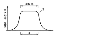
- the maximum energy intensity of the pulse laser can be calculated by averaging the intensity of the flat portion. Further, usually, on both sides of the flat portion, there are steepness portions whose strength gradually decreases toward the outside.
- the minimum number of times of irradiation when the crystal grain size growth is saturated by the irradiation of the pulse laser with the irradiation energy density E of the pulse laser is n0.
- the irradiation pulse energy density E is lower than the irradiation pulse energy density at which microcrystallization occurs in the non-single-crystal semiconductor film by irradiation with a pulse laser. Whether or not microcrystallization occurs can be determined by an electron micrograph or the like. If the irradiation pulse energy density is set to a value larger than the value at which microcrystallization occurs, the crystal grain size becomes extremely small, and the electron mobility as a semiconductor becomes about 1/10.
- the fact that the crystal grain size growth is saturated by irradiation with a pulse laser having an irradiation pulse energy density E means a state in which individual grain sizes are uniform and the grain size does not increase even when the number of irradiations is increased. Further, if the number of times of laser irradiation does not reach (n0-1), the crystal grain size does not grow sufficiently, and crystals with different grain sizes are mixed, resulting in variations in electron mobility. For the same reason, it is preferably n0 or more. The number of times of laser irradiation n is desirably 3 ⁇ n0 or less. If it exceeds 3 ⁇ n0, the productivity is significantly reduced. Furthermore, 2 ⁇ n0 or less is more desirable for the same reason.
- the scanning pitch of the pulse laser that is, the movement amount c for each pulse is less than b.
- the number of laser pulse seams appearing in each channel region is one or two or more, and variations in transistor performance can be reduced.
- the movement amount c is less than b / 2
- the number of seams in the channel region is n or (n + 1) or more (where n is an integer of 2 or more).
- the movement amount c is larger than b, the number of seams in the channel region becomes zero or one, and the performance variation of the transistor in the channel region increases.
- the transistor may be one in which a channel region is formed when pulsed laser irradiation is performed, or may be one in which a channel region is formed thereafter.
- the channel length of the semiconductor film targeted by the present invention is 100 ⁇ m or less. Within this range, the present invention is not particularly limited, but a channel length of 6 to 40 ⁇ m can be preferably shown.
- This beam width is preferably 100 to 500 ⁇ m. If the beam width is made too large, the beam length in the major axis direction of the pulse laser becomes small when the energy density is made constant, so that the area that can be processed in one scan is reduced and the processing efficiency is lowered. On the other hand, when the beam width is less than 100 ⁇ m, the scanning pitch is reduced and the production efficiency is lowered.
- distance for every pulse is not limited to a specific amount as this invention, 5 micrometers or more can be illustrated suitably.
- the semiconductor to be processed in the present invention is not limited to a specific material, but Si can be cited as a suitable material.
- An excimer laser can be cited as a suitable pulse laser.
- the manufacturing method of the present invention includes a method for modifying a crystalline semiconductor film such as single crystallization.
- a line having a beam short axis width of 100 to 500 ⁇ m and a flat portion in the beam cross-sectional direction in the beam short axis direction with respect to the non-single crystal semiconductor film is a line having a beam short axis width of 100 to 500 ⁇ m and a flat portion in the beam cross-sectional direction in the beam short axis direction with respect to the non-single crystal semiconductor film.
- the channel length of the transistor formed in the semiconductor film is b (100 ⁇ m or less)
- the pulse laser has an irradiation pulse energy density E that is lower than an irradiation pulse energy density at which microcrystallization occurs in the non-single-crystal semiconductor film by the irradiation of the pulse laser and at which a crystal grain size growth is saturated by a plurality of irradiations.
- n is (n0-1) or more, where n0 is the number of times of irradiation when the crystal grain size growth is saturated by irradiation of the pulse laser having the irradiation pulse energy density E. Since the scanning direction of the pulse laser is the channel length direction of the transistor and the movement amount c for each pulse is less than b, the laser annealing process can be efficiently performed with an appropriate number of pulse laser irradiations and the movement amount for each pulse. It can be carried out. In addition, variation in transistor characteristics due to beam edge irradiation can be reduced.
- FIG. 1 shows a state in which a substrate placed on a moving table 1 is irradiated with a pulse laser 3 made of a line beam excimer laser.
- a non-single-crystal semiconductor film 2 such as amorphous Si having a thickness of 35 to 55 nm is formed on the substrate.
- the film thickness is not limited to the above range.
- the pulse laser 3 has a line beam length L and a beam width a. By moving the movable table 1 at a predetermined pitch, the pulse laser 3 is scanned with the non-single crystal at a predetermined pitch and the number of irradiation times.
- the semiconductor film 2 is irradiated.
- FIG. 2 shows a beam cross-sectional shape of the pulse laser 3 in the scanning direction. It has a high intensity region having an energy intensity of 96% or more with respect to the maximum energy intensity, and most of the high intensity region is a flat portion. The width of the flat portion is indicated as a beam width a.
- the pulse laser 3 is set to an irradiation pulse energy density E that does not cause the non-single crystal semiconductor film 2 to be microcrystallized when the non-single crystal semiconductor film 2 is irradiated.
- the irradiation pulse energy density include 320 to 420 mJ / cm 2 .
- the irradiation pulse energy density is not limited to a specific range.
- FIG. 3 is a diagram showing the relationship between the irradiation pulse energy density and the crystal grain size due to laser pulse irradiation. In the region where the irradiation pulse energy density is low, the crystal grain size increases as the irradiation pulse energy density increases.
- the irradiation pulse energy density E becomes larger than the irradiation pulse energy density E1 in the middle of the process, the crystal grain size rapidly increases.
- the irradiation pulse energy density E2 is exceeded, the crystal grain size rapidly increases. It becomes small and microcrystallization occurs. Therefore, the irradiation pulse energy density E can be expressed by E ⁇ E2.
- FIG. 4 is a diagram showing the relationship of the crystal grain size with respect to the number of irradiations when the irradiation pulse energy density E is set to the irradiation pulse energy density E1 or the irradiation pulse energy density E2.
- the crystal grain size increases as the number of irradiations increases, but at a certain number of irradiations, the crystal grain size growth does not progress any further and is saturated. To do.
- This number of times of irradiation is shown as the number of times of irradiation n0 in the present invention.
- the actual number of irradiations n is set to (n0-1) or more and 3.n0 or less with respect to the number of irradiations n0. Thereby, the non-single-crystal semiconductor film 2 can be crystallized effectively and efficiently.
- FIG. 5 shows a planned arrangement state of the thin film semiconductors 10 on the non-single crystal semiconductor film 2.
- Each thin film semiconductor 10 has a source 11, a drain 12, and a channel portion 13 located between the source and drain, and the scanning direction of the pulse laser in the channel portion 13 is a channel length b.
- FIG. 5A shows the state of occurrence of the beam joint 3a when the movement amount c for each pulse is larger than the channel length b.
- the beam seam 3a is not positioned in the channel portion 13 (0) or one, so that the performance variation of the thin film semiconductor 10 is increased.
- FIG. 5B shows the state of occurrence of the beam joint 3a when the movement amount c for each pulse is 1 ⁇ 2 or more of the channel length b and less than the channel length b.
- one or two beam joints 3a appear in the channel portion 13, and the performance variation of the thin film semiconductor 10 is greatly reduced as compared with FIG.
- FIG. 5C shows the state of occurrence of the beam joint 3a when the movement amount c for each pulse is less than 1 ⁇ 2 of the channel region width b.
- n or (n + 1) or more (n is an integer of 2 or more) beam joints 3a appear in the channel portion 13, and the performance variation of the thin film semiconductor 10 is remarkably reduced.
- Amorphous Si with a thickness of 50 nm was used as a non-single crystal semiconductor film, and irradiation with a pulsed laser was performed under the following conditions while changing the number of irradiations.
- Excimer laser LSX315C / wavelength 308nm, frequency 300Hz
- Beam size beam length 500 mm x beam width 0.16 mm
- the beam width is a flat part in a high intensity region where the maximum energy intensity is 96% or more.
- Scan pitch 40 ⁇ m to 8 ⁇ m
- Irradiation pulse energy density 370 mJ / cm 2 Channel length: 20 ⁇ m
- the irradiation pulse energy density is lower than the irradiation pulse energy density at which microcrystals are generated, and it is recognized that the crystal grain diameter gradually grows from 4 times to 8 times.
- the crystal grain size growth is saturated after the number of irradiation times of 8 or more.
- FIG. 6 shows the change in crystal grain size according to the number of irradiations, and the crystal grain size increases as the number of irradiations increases until the number of irradiations reaches eight. No increase in crystal grain size was observed after 8 irradiations.
- an arbitrary number of irradiations that is, the amount of movement between pulses can be determined when the number of irradiations is eight or more. In nine irradiations, the amount of movement is less than the channel length. The amount is less than channel length / 2.
Landscapes
- Recrystallisation Techniques (AREA)
- Thin Film Transistor (AREA)
- Physics & Mathematics (AREA)
- Optics & Photonics (AREA)
Abstract
非単結晶半導体膜をレーザアニールする際に、適切な走査ピッチと照射回数によって半導体膜を結晶化するため、非単結晶半導体膜に対し、短軸幅100~500μmで短軸方向のビーム断面形状に平坦部を有するラインビーム形状のパルスレーザを相対的に走査することでパルス毎に移動させ、照射回数nでオーバーラップ照射する製造方法であって、トランジスタのチャンネル長をbとして、パルスレーザは、パルスレーザの照射により非単結晶半導体膜に微結晶化が生じる照射パルスエネルギ密度より低く、複数回数照射により結晶粒径成長が飽和する照射パルスエネルギ密度Eを有し、照射回数nは、照射パルスエネルギ密度Eのパルスレーザ照射によって結晶粒径成長が飽和する照射回数をn0として(n0-1)以上とし、パルスレーザの走査方向を前記トランジスタのチャンネル長方向とし、かつ前記パルス毎の移動量cをb未満とする。
Description
この発明は、非単結晶半導体膜上に、ラインビーム形状のパルスレーザを移動させつつ複数回照射(オーバラップ照射)する結晶半導体膜の製造方法に関するものである。
一般的にTVやPCディスプレイで用いられている薄膜トランジスタは、アモルファス(非結晶)シリコン(以降a-シリコンという)により構成されているが、何らかの手段でシリコンを結晶化(以降p-シリコンという)して利用することでTFTとしての性能を格段に向上させることができる。現在は、低温度でのSi結晶化プロセスとしてエキシマレーザアニール技術がすでに実用化されており、携帯電話等の小型ディスプレイ向け用途で頻繁に利用されており、さらに大画面ディスプレイなどへの実用化がなされている。
このレーザアニール法では、高いパルスエネルギを持つエキシマレーザを非単結晶半導体膜に照射することで、光エネルギを吸収した半導体が溶融または半溶融状態になり、その後急速に冷却され凝固する際に結晶化する仕組みである。この際には、広い領域を処理するために、ラインビーム形状に整形したパルスレーザを相対的に短軸方向に走査しながら照射する。通常は、単結晶半導体膜を設置した設置台を移動させることでパルスレーザの走査が行われる。
このレーザアニール法では、高いパルスエネルギを持つエキシマレーザを非単結晶半導体膜に照射することで、光エネルギを吸収した半導体が溶融または半溶融状態になり、その後急速に冷却され凝固する際に結晶化する仕組みである。この際には、広い領域を処理するために、ラインビーム形状に整形したパルスレーザを相対的に短軸方向に走査しながら照射する。通常は、単結晶半導体膜を設置した設置台を移動させることでパルスレーザの走査が行われる。
上記パルスレーザの走査においては、非単結晶半導体膜の同一位置にパルスレーザが複数回照射(オーバーラップ照射)されるように、所定のピッチでパルスレーザを走査方向に移動させている(例えば特許文献1参照)。これにより、サイズの大きい半導体膜のレーザアニール処理を可能にしている。なお、特許文献1では、レーザの順次走査に伴う結晶性の不均一性(ばらつき)が素子間のばらつきを生じさせる原因となることを課題にしている。そしてこの課題解決のため、特許文献1では、パルスレーザの走査方向におけるチャンネル領域のサイズSと、パルスレーザの走査ピッチPとが概略S=nP(nは0を除く整数)となるようにして、結晶性Si膜の結晶分布がパルスレーザ光の走査方向に周期的に変化するパターンとし、各薄膜トランジスタのチャンネル領域における結晶性Si膜は、結晶性分布のパターンの周期的な変化が等しくなるようにしている。
しかし、走査ピッチをチャンネル領域のサイズに合わせてサイズの整数倍に制御することは精度的に困難性を伴うものであり、高精度の走査を行うものとすれば装置コストが大幅にアップしてしまう。
ビームの短軸方向幅が十分にあれば走査ピッチを大きくすることができ、チャンネル領域にパルス毎のビームエッジができるだけ掛からないようにすることができる。しかし、この状態では、ビームエッジの照射がチャンネル領域に1回されたトランジスタとビームエッジの照射がチャンネル領域にされていない(0回)トランジスタとが併存し、トランジスタ間で特性にバラツキが生じてしまう。
ビームの短軸方向幅が十分にあれば走査ピッチを大きくすることができ、チャンネル領域にパルス毎のビームエッジができるだけ掛からないようにすることができる。しかし、この状態では、ビームエッジの照射がチャンネル領域に1回されたトランジスタとビームエッジの照射がチャンネル領域にされていない(0回)トランジスタとが併存し、トランジスタ間で特性にバラツキが生じてしまう。
このため、走査ピッチを小さくして、チャンネル領域においてパルス毎のビームエッジが所定回数必ず照射されるようにして結晶性のバラツキを小さくすることができる。これによれば、上記エッジの照射がなされたトランジスタとエッジ部分の照射がされていないトランジスタとの併存はなくなる。また、回数の相違も1回に抑えられるため、エッジの照射有無に比べれば、特性のバラツキは格段に小さくなる。
このようなエッジ部分で照射された半導体上の線状の領域では、チャンネルにおけるキャリアの移動に影響が生じると考えられるため、線状のエッジがチャンネル幅と直交する方向、すなわち、チャンネル内でのキャリアの移動方向に沿って位置するようにパルスレーザの走査方向を設定することが考えられる。これによりビームエッジの照射が行われていないチャンネル領域の部分で良好なキャリア移動の特性が期待される。
しかし、上記走査方向においては、チャンネル幅がチャンネル長以下(チャンネル幅/チャンネル長が1以下)であるようなトランジスタでは、(チャンネル幅/チャンネル長が1超)のものに比べてチャンネル幅が相対的に小さくなっているので、チャンネル領域において上記エッジが照射された線状の領域とエッジが照射されていない領域とが幅方向に併存する。これによりチャンネル幅方向で抵抗などの不均一性が生じ、キャリアの移動において幅方向で不均一性が生じトランジスタ特性に影響を与えるおそれがあるという問題がある。また、エッジがソースやドレインの一部に掛かって幅方向の不均一性を招くという問題もある。
本願発明は、上記事情を背景としてなされたものであり、高精度のパルスレーザの走査を要することなくトランジスタの特性のバラツキを低減して結晶化などを良好に行うことができる結晶半導体膜の製造方法を提供することを目的とする。
すなわち、本発明の結晶半導体膜の製造方法は、非単結晶半導体膜に対し、ビーム短軸幅が100~500μmでビーム短軸方向のビーム断面形状に平坦部を有するラインビーム形状のパルスレーザを相対的に走査することでパルス毎に移動させ、照射回数nで前記非単結晶半導体膜にオーバーラップ照射する結晶半導体膜の製造方法であって、
前記半導体膜に形成されるトランジスタのチャンネル長をb(100μm以下)として、
前記パルスレーザは、該パルスレーザの照射によって前記非単結晶半導体膜に微結晶化が生じる照射パルスエネルギ密度よりも低く、かつ複数回数の照射によって結晶粒径成長が飽和する照射パルスエネルギ密度Eを有し、
前記パルスレーザの照射回数nは、前記照射パルスエネルギ密度Eのパルスレーザの照射によって前記結晶粒径成長が飽和する際の照射回数をn0として(n0-1)以上とし、
前記パルスレーザの走査方向を前記トランジスタのチャンネル長方向とし、かつ前記パルス毎の移動量cをb未満とすることを特徴とする。
前記半導体膜に形成されるトランジスタのチャンネル長をb(100μm以下)として、
前記パルスレーザは、該パルスレーザの照射によって前記非単結晶半導体膜に微結晶化が生じる照射パルスエネルギ密度よりも低く、かつ複数回数の照射によって結晶粒径成長が飽和する照射パルスエネルギ密度Eを有し、
前記パルスレーザの照射回数nは、前記照射パルスエネルギ密度Eのパルスレーザの照射によって前記結晶粒径成長が飽和する際の照射回数をn0として(n0-1)以上とし、
前記パルスレーザの走査方向を前記トランジスタのチャンネル長方向とし、かつ前記パルス毎の移動量cをb未満とすることを特徴とする。
第2の本発明の結晶半導体膜の製造方法は、前記第1の本発明において、前記パルスレーザ照射回数nは、(n0-1)以上、3・n0以下であることを特徴とする。
第3の本発明の結晶半導体膜の製造方法は、前記第1または第2の本発明において、前記移動量がb/2未満であることを特徴とする。
第4の本発明の結晶半導体膜の製造方法は、前記第1~第3の本発明のいずれかにおいて、前記移動量が5μm以上であることを特徴とする。
第5の本発明の結晶半導体膜の製造方法は、前記第1~第4の本発明のいずれかにおいて、前記トランジスタのチャンネル幅とチャンネル長の比(チャンネル幅/チャンネル長)が1以下であることを特徴とする。
第6の本発明の結晶半導体膜の製造方法は、前記第1~第5の本発明のいずれかにおいて、前記非単結晶半導体がSiであることを特徴とする。
第7の本発明の結晶半導体膜の製造方法は、前記第1~第6の本発明のいずれかにおいて、前記パルスレーザがエキシマレーザであることを特徴とする。
上記パルスレーザは、上記したように、短軸方向のビーム断面形状に強度が平坦な平坦部(ビーム幅a)を有している。この平坦部の強度を平均化することでパルスレーザの最大エネルギ強度を算出することができる。また、通常、平坦部の両側には、外側に向けて次第に強度が低下するスティープネス部を有している。
上記パルスレーザの照射パルスエネルギ密度Eのパルスレーザの照射によって結晶粒径成長が飽和する際の照射回数の最小回数をn0とする。なお、照射パルスエネルギ密度Eは、パルスレーザの照射によって前記非単結晶半導体膜に微結晶化が生じる照射パルスエネルギ密度よりも低い値とする。微結晶化が生じるか否かは、電子顕微鏡写真等により判定することができる。
照射パルスエネルギ密度を微結晶化が生じる値よりも大きな値とすると、結晶粒径が極端に小さくなり、半導体としての電子移動度が1/10程度になってしまう。
また、照射パルスエネルギ密度Eのパルスレーザの照射によって結晶粒径成長が飽和するとは、個々の粒径が揃い、照射回数を増しても粒径が大きくならない状態をいう。
さらに、レーザ照射回数が、(n0-1)に達しないと、結晶粒径の成長が十分になされず、異なる粒径の結晶が混在し、電子移動度のバラツキが生じる。同様の理由で望ましくはn0以上である。
また、レーザ照射回数nは、3・n0以下とするのが望ましい。3・n0を越えると、著しく生産性が低下する。さらには、同様の理由で、2・n0以下が一層望ましい。
照射パルスエネルギ密度を微結晶化が生じる値よりも大きな値とすると、結晶粒径が極端に小さくなり、半導体としての電子移動度が1/10程度になってしまう。
また、照射パルスエネルギ密度Eのパルスレーザの照射によって結晶粒径成長が飽和するとは、個々の粒径が揃い、照射回数を増しても粒径が大きくならない状態をいう。
さらに、レーザ照射回数が、(n0-1)に達しないと、結晶粒径の成長が十分になされず、異なる粒径の結晶が混在し、電子移動度のバラツキが生じる。同様の理由で望ましくはn0以上である。
また、レーザ照射回数nは、3・n0以下とするのが望ましい。3・n0を越えると、著しく生産性が低下する。さらには、同様の理由で、2・n0以下が一層望ましい。
上記パルスレーザの照射がおこなわれる半導体膜上のトランジスタのチャンネル長をbとすると、パルスレーザの走査ピッチ、すなわちパルス毎の移動量cは、b未満とする。これにより、各チャンネル領域で現れるレーザパルスの継ぎ目は1本または2本以上となり、トランジスタの性能ばらつきを低減することができる。一方、移動量cがb/2未満であると、チャンネル領域における前記継ぎ目はn本または(n+1)本以上(但しnは2以上の整数)になる。移動量cがbよりも大きくなるとチャンネル領域における前記継ぎ目は0本もしくは1本になり、チャンネル領域でのトランジスタの性能ばらつきが大きくなる。
なお、トランジスタは、パルスレーザの照射に際し、チャンネル領域が形成されているものであってもよく、また、その後チャンネル領域が形成されるものであってもよい。
なお、本発明が対象とする半導体膜のチャンネル長は100μm以下とされる。なお、この範囲であれば本発明としては特に限定されるものではないが、好適には6~40μmのチャンネル長を示すことができる。
なお、本発明が対象とする半導体膜のチャンネル長は100μm以下とされる。なお、この範囲であれば本発明としては特に限定されるものではないが、好適には6~40μmのチャンネル長を示すことができる。
上記レーザ照射回数nおよびパルス毎の移動量cによって、パルスレーザのビーム幅aは、a=n・cで示される。このビーム幅は、100~500μmとするのが望ましい。ビーム幅を大きくしすぎると、エネルギ密度を一定にする場合、パルスレーザの長軸方向におけるビーム長が小さくなるので、一走査で処理できる面積が小さくなり、処理効率が低下する。また、ビーム幅が100μm未満になると、走査ピッチが小さくなり、生産効率が低下する。
なお、パルス毎の移動量は、本発明としては特定の量に限定されるものではないが、好適には5μm以上を例示することができる。
なお、パルス毎の移動量は、本発明としては特定の量に限定されるものではないが、好適には5μm以上を例示することができる。
本発明の処理対象となる半導体は、特定の材質に限定されないが、Siを好適なものとして挙げることができる。また、パルスレーザとしては、エキシマレーザを好適なものとして挙げることができる。また、本発明の製造方法では、非晶質の半導体膜を結晶化させるものの他、結晶質の半導体膜を単結晶化などの改質を行うものも含まれる。
以上説明したように、本発明の結晶半導体膜の製造方法によれば、非単結晶半導体膜に対し、ビーム短軸幅が100~500μmでビーム短軸方向のビーム断面形状に平坦部を有するラインビーム形状のパルスレーザを相対的に走査することでパルス毎に移動させ、照射回数nで前記非単結晶半導体膜にオーバーラップ照射して結晶化を行う結晶半導体膜の製造方法であって、
前記半導体膜に形成されるトランジスタのチャンネル長をb(100μm以下)として、
前記パルスレーザは、該パルスレーザの照射によって前記非単結晶半導体膜に微結晶化が生じる照射パルスエネルギ密度よりも低く、かつ複数回数の照射によって結晶粒径成長が飽和する照射パルスエネルギ密度Eを有し、
前記パルスレーザの照射回数nは、前記照射パルスエネルギ密度Eのパルスレーザの照射によって前記結晶粒径成長が飽和する際の照射回数をn0として(n0-1)以上とし、
前記パルスレーザの走査方向を前記トランジスタのチャンネル長方向とし、かつ前記パルス毎の移動量cをb未満とするので、適正なパルスレーザ照射回数およびパルス毎の移動量により効率的にレーザアニール処理を行うことができる。また、ビームエッジの照射によるトランジスタ特性のバラツキを小さくすることができる。
前記半導体膜に形成されるトランジスタのチャンネル長をb(100μm以下)として、
前記パルスレーザは、該パルスレーザの照射によって前記非単結晶半導体膜に微結晶化が生じる照射パルスエネルギ密度よりも低く、かつ複数回数の照射によって結晶粒径成長が飽和する照射パルスエネルギ密度Eを有し、
前記パルスレーザの照射回数nは、前記照射パルスエネルギ密度Eのパルスレーザの照射によって前記結晶粒径成長が飽和する際の照射回数をn0として(n0-1)以上とし、
前記パルスレーザの走査方向を前記トランジスタのチャンネル長方向とし、かつ前記パルス毎の移動量cをb未満とするので、適正なパルスレーザ照射回数およびパルス毎の移動量により効率的にレーザアニール処理を行うことができる。また、ビームエッジの照射によるトランジスタ特性のバラツキを小さくすることができる。
以下に、本発明の一実施形態を説明する。
図1は、移動台1上に載置された基板にラインビーム状のエキシマレーザからなるパルスレーザ3が照射されている状態を示している。基板には、例えば膜厚35~55nmのアモルファスSiなどの非単結晶半導体膜2が形成されている。なお、本発明としては、膜厚が上記範囲に限定されるものではない。
パルスレーザ3は、ラインビーム長Lおよびビーム幅aを有しており、移動台1を所定のピッチで移動させることで、パルスレーザ3が走査されつつ、所定のピッチおよび照射回数で非単結晶半導体膜2上に照射される。なお、パルスレーザ3の走査は、非単結晶半導体膜2に対し相対的に行われるものであればよく、上記のように非単結晶半導体膜2を移動させることで実現してもよく、パルスレーザ3側を移動させるものであってもよい。また、両者を組み合わせることも可能である。
図2は、パルスレーザ3の走査方向のビーム断面形状を示すものである。最大エネルギ強度に対し、96%以上のエネルギ強度を有する高強度領域を有し、該高強度領域の殆どが平坦部になっている。該平坦部の幅がビーム幅aとして示される。
図1は、移動台1上に載置された基板にラインビーム状のエキシマレーザからなるパルスレーザ3が照射されている状態を示している。基板には、例えば膜厚35~55nmのアモルファスSiなどの非単結晶半導体膜2が形成されている。なお、本発明としては、膜厚が上記範囲に限定されるものではない。
パルスレーザ3は、ラインビーム長Lおよびビーム幅aを有しており、移動台1を所定のピッチで移動させることで、パルスレーザ3が走査されつつ、所定のピッチおよび照射回数で非単結晶半導体膜2上に照射される。なお、パルスレーザ3の走査は、非単結晶半導体膜2に対し相対的に行われるものであればよく、上記のように非単結晶半導体膜2を移動させることで実現してもよく、パルスレーザ3側を移動させるものであってもよい。また、両者を組み合わせることも可能である。
図2は、パルスレーザ3の走査方向のビーム断面形状を示すものである。最大エネルギ強度に対し、96%以上のエネルギ強度を有する高強度領域を有し、該高強度領域の殆どが平坦部になっている。該平坦部の幅がビーム幅aとして示される。
また、パルスレーザ3は、非単結晶半導体膜2に照射される際に、該非単結晶半導体膜2が微結晶化しない照射パルスエネルギ密度Eに設定されている。照射パルスエネルギ密度としては、例えば320~420mJ/cm2が例示される。但し、本発明としては、照射パルスエネルギ密度が特定の範囲に限定されるものではない。
図3は、照射パルスエネルギ密度とレーザパルスの照射による結晶粒径の大きさの関係を示す図である。照射パルスエネルギ密度が低い領域では、照射パルスエネルギ密度が増すに連れて結晶粒径が大きくなっている。例えば、その途中の照射パルスエネルギ密度E1よりも照射パルスエネルギ密度が大きくなると結晶粒径が急激に大きくなる。一方、照射パルスエネルギ密度がある程度に迄大きくなると、それ以上に照射パルスエネルギ密度が大きくなっても結晶粒径の増大は殆どなく、ある照射パルスエネルギ密度E2を越えると、結晶粒径が急激に小さくなって微結晶化が生じる。したがって上記照射パルスエネルギ密度Eは、E≦E2で示すことができる。
図3は、照射パルスエネルギ密度とレーザパルスの照射による結晶粒径の大きさの関係を示す図である。照射パルスエネルギ密度が低い領域では、照射パルスエネルギ密度が増すに連れて結晶粒径が大きくなっている。例えば、その途中の照射パルスエネルギ密度E1よりも照射パルスエネルギ密度が大きくなると結晶粒径が急激に大きくなる。一方、照射パルスエネルギ密度がある程度に迄大きくなると、それ以上に照射パルスエネルギ密度が大きくなっても結晶粒径の増大は殆どなく、ある照射パルスエネルギ密度E2を越えると、結晶粒径が急激に小さくなって微結晶化が生じる。したがって上記照射パルスエネルギ密度Eは、E≦E2で示すことができる。
照射パルスエネルギ密度を上記Eの値に設定して、非単結晶半導体膜2に照射する際には、ある回数以上に照射回数を設定しても、結晶粒径成長が飽和する。結晶粒径成長の飽和は、SEM写真により判定する。
図4は、照射パルスエネルギ密度Eを、上記照射パルスエネルギ密度E1または照射パルスエネルギ密度E2に設定した場合に、照射回数に対する結晶粒径の関係を示す図である。いずれの照射パルスエネルギ密度の場合も、ある照射回数までは、照射回数が増加するに連れて結晶粒径が大きくなるが、ある照射回数になると結晶粒径成長はそれ以上には進行せず飽和する。この照射回数が本発明における照射回数n0として示される。
実際の照射回数nは、前記照射回数n0に対し、(n0-1)以上、3・n0以下に設定する。これにより、非単結晶半導体膜2を効果的かつ効率的に結晶化することができる。
図4は、照射パルスエネルギ密度Eを、上記照射パルスエネルギ密度E1または照射パルスエネルギ密度E2に設定した場合に、照射回数に対する結晶粒径の関係を示す図である。いずれの照射パルスエネルギ密度の場合も、ある照射回数までは、照射回数が増加するに連れて結晶粒径が大きくなるが、ある照射回数になると結晶粒径成長はそれ以上には進行せず飽和する。この照射回数が本発明における照射回数n0として示される。
実際の照射回数nは、前記照射回数n0に対し、(n0-1)以上、3・n0以下に設定する。これにより、非単結晶半導体膜2を効果的かつ効率的に結晶化することができる。
上記パルスレーザの照射によって結晶化された結晶化半導体膜では、所定の間隔で薄膜半導体が形成される。該間隔は、好適には1mm以下に設定される。また、薄膜半導体では、それぞれ所定のチャンネル長bを有しており、チャンネル長bは、100μm以下、好適には6~40μmの長さに設計される。
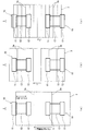
非単結晶半導体膜2上における薄膜半導体10の配列予定状態を図5に示す。各薄膜半導体10では、ソース11、ドレイン12、ソース、ドレイン間に位置するチャンネル部13を有しており、該チャンネル部13のパルスレーザの走査方向が、チャンネル長bとなっている。上記非単結晶半導体膜2に対し走査ピッチ(パルス毎の移動量)cによってパルスレーザ3を照射、移動させると、パルス毎の移動に応じて結晶化半導体膜上にビームの継ぎ目3aが現れる。
非単結晶半導体膜2上における薄膜半導体10の配列予定状態を図5に示す。各薄膜半導体10では、ソース11、ドレイン12、ソース、ドレイン間に位置するチャンネル部13を有しており、該チャンネル部13のパルスレーザの走査方向が、チャンネル長bとなっている。上記非単結晶半導体膜2に対し走査ピッチ(パルス毎の移動量)cによってパルスレーザ3を照射、移動させると、パルス毎の移動に応じて結晶化半導体膜上にビームの継ぎ目3aが現れる。
図5(a)は、パルス毎の移動量cを前記チャンネル長bよりも大きくした場合のビーム継ぎ目3aの発生状況を示している。この例では、ビーム継ぎ目3aは、チャンネル部13に位置しないか(0本)、1本現れることになり、薄膜半導体10の性能ばらつきを大きくする。
図5(b)は、パルス毎の移動量cを前記チャンネル長bの1/2以上で、チャンネル長b未満とした場合のビーム継ぎ目3aの発生状況を示している。この例では、ビーム継ぎ目3aは、チャンネル部13に1本または2本現れることになり、薄膜半導体10の性能ばらつきは図5(a)に比べて大幅に低減される。
図5(c)は、パルス毎の移動量cを前記チャンネル領域幅bの1/2未満にした場合のビーム継ぎ目3aの発生状況を示している。この例では、ビーム継ぎ目3aは、チャンネル部13にn本または(n+1)本以上(但しnは2以上の整数)現れることになり、薄膜半導体10の性能ばらつきは顕著に低減される。
図5(b)は、パルス毎の移動量cを前記チャンネル長bの1/2以上で、チャンネル長b未満とした場合のビーム継ぎ目3aの発生状況を示している。この例では、ビーム継ぎ目3aは、チャンネル部13に1本または2本現れることになり、薄膜半導体10の性能ばらつきは図5(a)に比べて大幅に低減される。
図5(c)は、パルス毎の移動量cを前記チャンネル領域幅bの1/2未満にした場合のビーム継ぎ目3aの発生状況を示している。この例では、ビーム継ぎ目3aは、チャンネル部13にn本または(n+1)本以上(但しnは2以上の整数)現れることになり、薄膜半導体10の性能ばらつきは顕著に低減される。
以下に、本発明の一実施例を説明する。
50nm厚のアモルファスSiを非単結晶半導体膜として、以下の条件で照射回数を変えてパルスレーザの照射を行った。
エキシマレーザ :LSX315C/波長308nm、周波数300Hz
ビームサイズ :ビーム長500mm×ビーム幅0.16mm
ビーム幅は、最大エネルギー強度96%以上の高強度域内の平坦部
スキャンピッチ :40μm~8μm
照射パルスエネルギ密度
:370mJ/cm2
チャンネル長 :20μm
50nm厚のアモルファスSiを非単結晶半導体膜として、以下の条件で照射回数を変えてパルスレーザの照射を行った。
エキシマレーザ :LSX315C/波長308nm、周波数300Hz
ビームサイズ :ビーム長500mm×ビーム幅0.16mm
ビーム幅は、最大エネルギー強度96%以上の高強度域内の平坦部
スキャンピッチ :40μm~8μm
照射パルスエネルギ密度
:370mJ/cm2
チャンネル長 :20μm
上記パルスレーザでは、照射パルスエネルギ密度は、微結晶が生じる照射パルスエネルギ密度以下になっており、照射回数4回から照射回数8回までは結晶粒径が次第に成長していることが認められるが、照射回数8回以降では結晶粒径成長が飽和する。
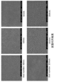
所定の照射回数でパルスレーザを照射した部位について、SEM写真により観察し、該写真を図6で示した。図6に示すように、照射回数8回で、良好に結晶化がなされており、照射回数を12、16、20回に増やした場合でも、結晶粒径の増加は殆ど見られなかった。
図7は、照射回数に応じた結晶粒径の変化を示すものであり、照射回数8回に至るまでは、照射回数の増加に応じて結晶粒径が増大している。照射回数8回以降では結晶粒径の増大は見られなかった。
したがって、照射回数8回以上で任意の照射回数、すなわちパルス間の移動量を決定することができ、9回の照射回数において、移動量は、チャンネル長未満となり、17回の照射回数において、移動量はチャンネル長/2未満になる。
図7は、照射回数に応じた結晶粒径の変化を示すものであり、照射回数8回に至るまでは、照射回数の増加に応じて結晶粒径が増大している。照射回数8回以降では結晶粒径の増大は見られなかった。
したがって、照射回数8回以上で任意の照射回数、すなわちパルス間の移動量を決定することができ、9回の照射回数において、移動量は、チャンネル長未満となり、17回の照射回数において、移動量はチャンネル長/2未満になる。
1 移動台
2 非単結晶半導体膜
3 パルスレーザ
3a ビーム継ぎ目
10 薄膜半導体
11 ソース
12 ドレイン
13 チャンネル部
2 非単結晶半導体膜
3 パルスレーザ
3a ビーム継ぎ目
10 薄膜半導体
11 ソース
12 ドレイン
13 チャンネル部
Claims (7)
- 非単結晶半導体膜に対し、ビーム短軸幅が100~500μmでビーム短軸方向のビーム断面形状に平坦部を有するラインビーム形状のパルスレーザを相対的に走査することでパルス毎に移動させ、照射回数nで前記非単結晶半導体膜にオーバーラップ照射する結晶半導体膜の製造方法であって、
前記半導体膜に形成されるトランジスタのチャンネル長をb(100μm以下)として、
前記パルスレーザは、該パルスレーザの照射によって前記非単結晶半導体膜に微結晶化が生じる照射パルスエネルギ密度よりも低く、かつ複数回数の照射によって結晶粒径成長が飽和する照射パルスエネルギ密度Eを有し、
前記パルスレーザの照射回数nは、前記照射パルスエネルギ密度Eのパルスレーザの照射によって前記結晶粒径成長が飽和する際の照射回数をn0として(n0-1)以上とし、
前記パルスレーザの走査方向を前記トランジスタのチャンネル長方向とし、かつ前記パルス毎の移動量cをb未満とすることを特徴とする結晶半導体膜の製造方法。 - 前記パルスレーザ照射回数nは、(n0-1)以上、3・n0以下であることを特徴とする請求項1記載の結晶半導体膜の製造方法。
- 前記移動量がb/2未満であることを特徴とする請求項1または2に記載の結晶半導体膜の製造方法。
- 前記移動量が5μm以上であることを特徴とする請求項1~3のいずれかに記載の結晶半導体膜の製造方法。
- 前記トランジスタのチャンネル幅とチャンネル長の比(チャンネル幅/チャンネル長)が1以下であることを特徴とする請求項1~4のいずれかに記載の結晶半導体膜の製造方法。
- 前記非単結晶半導体がSiであることを特徴とする請求項1~5のいずれかに記載の結晶半導体膜の製造方法。
- 前記パルスレーザがエキシマレーザであることを特徴とする請求項1~6のいずれかに記載の結晶半導体膜の製造方法。
Priority Applications (3)
| Application Number | Priority Date | Filing Date | Title |
|---|---|---|---|
| KR1020157014644A KR102111956B1 (ko) | 2012-12-18 | 2013-11-11 | 결정 반도체막의 제조 방법 |
| SG11201504654PA SG11201504654PA (en) | 2012-12-18 | 2013-11-11 | Manufacturing method of crystalline semiconductor film |
| CN201380065862.6A CN104871291B (zh) | 2012-12-18 | 2013-11-11 | 结晶半导体膜的制造方法 |
Applications Claiming Priority (2)
| Application Number | Priority Date | Filing Date | Title |
|---|---|---|---|
| JP2012276217A JP5918118B2 (ja) | 2012-12-18 | 2012-12-18 | 結晶半導体膜の製造方法 |
| JP2012-276217 | 2012-12-18 |
Publications (1)
| Publication Number | Publication Date |
|---|---|
| WO2014097770A1 true WO2014097770A1 (ja) | 2014-06-26 |
Family
ID=50978116
Family Applications (1)
| Application Number | Title | Priority Date | Filing Date |
|---|---|---|---|
| PCT/JP2013/080418 Ceased WO2014097770A1 (ja) | 2012-12-18 | 2013-11-11 | 結晶半導体膜の製造方法 |
Country Status (6)
| Country | Link |
|---|---|
| JP (1) | JP5918118B2 (ja) |
| KR (1) | KR102111956B1 (ja) |
| CN (1) | CN104871291B (ja) |
| SG (1) | SG11201504654PA (ja) |
| TW (1) | TWI606493B (ja) |
| WO (1) | WO2014097770A1 (ja) |
Cited By (1)
| Publication number | Priority date | Publication date | Assignee | Title |
|---|---|---|---|---|
| CN109643644A (zh) * | 2016-08-22 | 2019-04-16 | 万佳雷射有限公司 | 用于对半导体材料的层进行退火的设备、对半导体材料的层进行退火的方法以及平板显示器 |
Families Citing this family (5)
| Publication number | Priority date | Publication date | Assignee | Title |
|---|---|---|---|---|
| JP6086394B2 (ja) * | 2015-03-11 | 2017-03-01 | 株式会社ブイ・テクノロジー | 薄膜トランジスタ基板、表示パネル、レーザーアニール方法 |
| CN107924827B (zh) * | 2015-06-29 | 2022-07-01 | Ipg光子公司 | 用于非晶硅衬底的均匀结晶的基于光纤激光器的系统 |
| JP6687497B2 (ja) * | 2016-10-20 | 2020-04-22 | 株式会社日本製鋼所 | 結晶半導体膜製造方法、結晶半導体膜製造装置および結晶半導体膜製造装置の制御方法 |
| WO2018074282A1 (ja) * | 2016-10-20 | 2018-04-26 | 株式会社日本製鋼所 | レーザアニール方法およびレーザアニール装置 |
| JP6941473B2 (ja) | 2017-04-26 | 2021-09-29 | 株式会社日本製鋼所 | ディスプレイの製造方法、ディスプレイ及び液晶テレビ |
Citations (7)
| Publication number | Priority date | Publication date | Assignee | Title |
|---|---|---|---|---|
| JPH10163495A (ja) * | 1996-11-26 | 1998-06-19 | Sharp Corp | 半導体装置及びその製造方法 |
| JPH1164883A (ja) * | 1997-08-12 | 1999-03-05 | Toshiba Corp | 多結晶半導体薄膜の製造方法および製造装置 |
| JP2001093854A (ja) * | 1999-09-22 | 2001-04-06 | Sony Corp | 多結晶膜の製造方法および半導体装置の製造方法 |
| JP3276900B2 (ja) * | 1997-09-30 | 2002-04-22 | 三洋電機株式会社 | 半導体装置及び表示装置 |
| JP2002176063A (ja) * | 2000-09-29 | 2002-06-21 | Sanyo Electric Co Ltd | 半導体装置 |
| JP2002175029A (ja) * | 2000-09-29 | 2002-06-21 | Sanyo Electric Co Ltd | 半導体装置及び表示装置 |
| JP2011108987A (ja) * | 2009-11-20 | 2011-06-02 | Japan Steel Works Ltd:The | 結晶半導体膜の製造方法 |
Family Cites Families (5)
| Publication number | Priority date | Publication date | Assignee | Title |
|---|---|---|---|---|
| US6573161B1 (en) * | 1999-03-05 | 2003-06-03 | Seiko Epson Corporation | Thin film semiconductor device fabrication process |
| US6737672B2 (en) * | 2000-08-25 | 2004-05-18 | Fujitsu Limited | Semiconductor device, manufacturing method thereof, and semiconductor manufacturing apparatus |
| CN100485928C (zh) * | 2000-09-29 | 2009-05-06 | 三洋电机株式会社 | 半导体器件以及显示装置 |
| US7160762B2 (en) | 2002-11-08 | 2007-01-09 | Semiconductor Energy Laboratory Co., Ltd. | Method for manufacturing semiconductor device, semiconductor device, and laser irradiation apparatus |
| JP2011040594A (ja) * | 2009-08-12 | 2011-02-24 | Seiko Epson Corp | 薄膜トランジスターの製造方法 |
-
2012
- 2012-12-18 JP JP2012276217A patent/JP5918118B2/ja active Active
-
2013
- 2013-11-11 KR KR1020157014644A patent/KR102111956B1/ko active Active
- 2013-11-11 WO PCT/JP2013/080418 patent/WO2014097770A1/ja not_active Ceased
- 2013-11-11 SG SG11201504654PA patent/SG11201504654PA/en unknown
- 2013-11-11 CN CN201380065862.6A patent/CN104871291B/zh active Active
- 2013-11-28 TW TW102143352A patent/TWI606493B/zh not_active IP Right Cessation
Patent Citations (7)
| Publication number | Priority date | Publication date | Assignee | Title |
|---|---|---|---|---|
| JPH10163495A (ja) * | 1996-11-26 | 1998-06-19 | Sharp Corp | 半導体装置及びその製造方法 |
| JPH1164883A (ja) * | 1997-08-12 | 1999-03-05 | Toshiba Corp | 多結晶半導体薄膜の製造方法および製造装置 |
| JP3276900B2 (ja) * | 1997-09-30 | 2002-04-22 | 三洋電機株式会社 | 半導体装置及び表示装置 |
| JP2001093854A (ja) * | 1999-09-22 | 2001-04-06 | Sony Corp | 多結晶膜の製造方法および半導体装置の製造方法 |
| JP2002176063A (ja) * | 2000-09-29 | 2002-06-21 | Sanyo Electric Co Ltd | 半導体装置 |
| JP2002175029A (ja) * | 2000-09-29 | 2002-06-21 | Sanyo Electric Co Ltd | 半導体装置及び表示装置 |
| JP2011108987A (ja) * | 2009-11-20 | 2011-06-02 | Japan Steel Works Ltd:The | 結晶半導体膜の製造方法 |
Cited By (1)
| Publication number | Priority date | Publication date | Assignee | Title |
|---|---|---|---|---|
| CN109643644A (zh) * | 2016-08-22 | 2019-04-16 | 万佳雷射有限公司 | 用于对半导体材料的层进行退火的设备、对半导体材料的层进行退火的方法以及平板显示器 |
Also Published As
| Publication number | Publication date |
|---|---|
| JP5918118B2 (ja) | 2016-05-18 |
| TWI606493B (zh) | 2017-11-21 |
| KR20150096388A (ko) | 2015-08-24 |
| KR102111956B1 (ko) | 2020-05-18 |
| JP2014120686A (ja) | 2014-06-30 |
| CN104871291A (zh) | 2015-08-26 |
| SG11201504654PA (en) | 2015-07-30 |
| TW201430914A (zh) | 2014-08-01 |
| CN104871291B (zh) | 2018-06-19 |
Similar Documents
| Publication | Publication Date | Title |
|---|---|---|
| US7645337B2 (en) | Systems and methods for creating crystallographic-orientation controlled poly-silicon films | |
| JP5918118B2 (ja) | 結晶半導体膜の製造方法 | |
| KR101212378B1 (ko) | 결정 방위 제어형 폴리실리콘막을 생성하기 위한 장치 및 방법 | |
| WO2005029543A2 (en) | Laser-irradiated thin films having variable thickness | |
| JP2004311935A (ja) | 単結晶シリコン膜の製造方法 | |
| WO2010056990A1 (en) | Systems and methods for the crystallization of thin films | |
| JP4947667B2 (ja) | 結晶半導体膜の製造方法 | |
| KR100740124B1 (ko) | 다결정 실리콘 박막 트랜지스터 및 그 제조방법 | |
| US20020102821A1 (en) | Mask pattern design to improve quality uniformity in lateral laser crystallized poly-Si films | |
| JP2012243818A (ja) | レーザ処理装置 | |
| JP4691331B2 (ja) | 非晶質シリコン膜の結晶化方法 | |
| JP2005197658A (ja) | 多結晶シリコン膜の形成方法 | |
| JP6687497B2 (ja) | 結晶半導体膜製造方法、結晶半導体膜製造装置および結晶半導体膜製造装置の制御方法 | |
| KR20110103222A (ko) | 비정질 실리콘막의 결정화 방법 | |
| JP5339322B2 (ja) | レーザによるシリコン結晶成長方法 | |
| JP4365757B2 (ja) | 多結晶シリコン薄膜トランジスタの多結晶シリコン膜の形成方法 | |
| JP2005064134A (ja) | 薄膜半導体及びその形成方法 | |
| JP2007281465A (ja) | 多結晶膜の形成方法 | |
| CN101009219B (zh) | 硅结晶掩模、结晶硅的装置及使用其的方法 | |
| JP4881197B2 (ja) | 結晶化パターンおよびこれを用いた非晶質シリコンの結晶化方法 | |
| KR101915692B1 (ko) | 비정질 실리콘의 결정화 방법 |
Legal Events
| Date | Code | Title | Description |
|---|---|---|---|
| 121 | Ep: the epo has been informed by wipo that ep was designated in this application |
Ref document number: 13865028 Country of ref document: EP Kind code of ref document: A1 |
|
| ENP | Entry into the national phase |
Ref document number: 20157014644 Country of ref document: KR Kind code of ref document: A |
|
| NENP | Non-entry into the national phase |
Ref country code: DE |
|
| 122 | Ep: pct application non-entry in european phase |
Ref document number: 13865028 Country of ref document: EP Kind code of ref document: A1 |