WO2014057684A1 - ラダー化合物、及びそれを用いた有機エレクトロルミネッセンス素子 - Google Patents
ラダー化合物、及びそれを用いた有機エレクトロルミネッセンス素子 Download PDFInfo
- Publication number
- WO2014057684A1 WO2014057684A1 PCT/JP2013/006061 JP2013006061W WO2014057684A1 WO 2014057684 A1 WO2014057684 A1 WO 2014057684A1 JP 2013006061 W JP2013006061 W JP 2013006061W WO 2014057684 A1 WO2014057684 A1 WO 2014057684A1
- Authority
- WO
- WIPO (PCT)
- Prior art keywords
- group
- substituted
- unsubstituted
- carbon atoms
- organic
- Prior art date
- Legal status (The legal status is an assumption and is not a legal conclusion. Google has not performed a legal analysis and makes no representation as to the accuracy of the status listed.)
- Ceased
Links
- 0 C*c1c(*C)[n](C)c(*2)c1C(*C1=C(C(*=***)=C(*)N3C)C3=**)=C2C1=C Chemical compound C*c1c(*C)[n](C)c(*2)c1C(*C1=C(C(*=***)=C(*)N3C)C3=**)=C2C1=C 0.000 description 2
- VGBXIAFMCFRDPB-UHFFFAOYSA-N c(cc1)ccc1-[n]1c2c(c3ccccc3[n]3-c4ccc5[s]c6ccccc6c5c4)c3ccc2c(cc2)c1c(c1c3cccc1)c2[n]3-c(cc1)cc2c1[o]c1c2cccc1 Chemical compound c(cc1)ccc1-[n]1c2c(c3ccccc3[n]3-c4ccc5[s]c6ccccc6c5c4)c3ccc2c(cc2)c1c(c1c3cccc1)c2[n]3-c(cc1)cc2c1[o]c1c2cccc1 VGBXIAFMCFRDPB-UHFFFAOYSA-N 0.000 description 1
Images


Classifications
-
- C—CHEMISTRY; METALLURGY
- C07—ORGANIC CHEMISTRY
- C07D—HETEROCYCLIC COMPOUNDS
- C07D487/00—Heterocyclic compounds containing nitrogen atoms as the only ring hetero atoms in the condensed system, not provided for by groups C07D451/00 - C07D477/00
- C07D487/12—Heterocyclic compounds containing nitrogen atoms as the only ring hetero atoms in the condensed system, not provided for by groups C07D451/00 - C07D477/00 in which the condensed system contains three hetero rings
- C07D487/14—Ortho-condensed systems
-
- C—CHEMISTRY; METALLURGY
- C07—ORGANIC CHEMISTRY
- C07D—HETEROCYCLIC COMPOUNDS
- C07D491/00—Heterocyclic compounds containing in the condensed ring system both one or more rings having oxygen atoms as the only ring hetero atoms and one or more rings having nitrogen atoms as the only ring hetero atoms, not provided for by groups C07D451/00 - C07D459/00, C07D463/00, C07D477/00 or C07D489/00
- C07D491/12—Heterocyclic compounds containing in the condensed ring system both one or more rings having oxygen atoms as the only ring hetero atoms and one or more rings having nitrogen atoms as the only ring hetero atoms, not provided for by groups C07D451/00 - C07D459/00, C07D463/00, C07D477/00 or C07D489/00 in which the condensed system contains three hetero rings
- C07D491/14—Ortho-condensed systems
-
- C—CHEMISTRY; METALLURGY
- C07—ORGANIC CHEMISTRY
- C07D—HETEROCYCLIC COMPOUNDS
- C07D491/00—Heterocyclic compounds containing in the condensed ring system both one or more rings having oxygen atoms as the only ring hetero atoms and one or more rings having nitrogen atoms as the only ring hetero atoms, not provided for by groups C07D451/00 - C07D459/00, C07D463/00, C07D477/00 or C07D489/00
- C07D491/12—Heterocyclic compounds containing in the condensed ring system both one or more rings having oxygen atoms as the only ring hetero atoms and one or more rings having nitrogen atoms as the only ring hetero atoms, not provided for by groups C07D451/00 - C07D459/00, C07D463/00, C07D477/00 or C07D489/00 in which the condensed system contains three hetero rings
- C07D491/14—Ortho-condensed systems
- C07D491/147—Ortho-condensed systems the condensed system containing one ring with oxygen as ring hetero atom and two rings with nitrogen as ring hetero atom
-
- C—CHEMISTRY; METALLURGY
- C07—ORGANIC CHEMISTRY
- C07D—HETEROCYCLIC COMPOUNDS
- C07D491/00—Heterocyclic compounds containing in the condensed ring system both one or more rings having oxygen atoms as the only ring hetero atoms and one or more rings having nitrogen atoms as the only ring hetero atoms, not provided for by groups C07D451/00 - C07D459/00, C07D463/00, C07D477/00 or C07D489/00
- C07D491/22—Heterocyclic compounds containing in the condensed ring system both one or more rings having oxygen atoms as the only ring hetero atoms and one or more rings having nitrogen atoms as the only ring hetero atoms, not provided for by groups C07D451/00 - C07D459/00, C07D463/00, C07D477/00 or C07D489/00 in which the condensed system contains four or more hetero rings
-
- C—CHEMISTRY; METALLURGY
- C07—ORGANIC CHEMISTRY
- C07D—HETEROCYCLIC COMPOUNDS
- C07D495/00—Heterocyclic compounds containing in the condensed system at least one hetero ring having sulfur atoms as the only ring hetero atoms
- C07D495/12—Heterocyclic compounds containing in the condensed system at least one hetero ring having sulfur atoms as the only ring hetero atoms in which the condensed system contains three hetero rings
- C07D495/14—Ortho-condensed systems
-
- C—CHEMISTRY; METALLURGY
- C07—ORGANIC CHEMISTRY
- C07D—HETEROCYCLIC COMPOUNDS
- C07D495/00—Heterocyclic compounds containing in the condensed system at least one hetero ring having sulfur atoms as the only ring hetero atoms
- C07D495/22—Heterocyclic compounds containing in the condensed system at least one hetero ring having sulfur atoms as the only ring hetero atoms in which the condensed system contains four or more hetero rings
-
- C—CHEMISTRY; METALLURGY
- C07—ORGANIC CHEMISTRY
- C07D—HETEROCYCLIC COMPOUNDS
- C07D519/00—Heterocyclic compounds containing more than one system of two or more relevant hetero rings condensed among themselves or condensed with a common carbocyclic ring system not provided for in groups C07D453/00 or C07D455/00
-
- C—CHEMISTRY; METALLURGY
- C09—DYES; PAINTS; POLISHES; NATURAL RESINS; ADHESIVES; COMPOSITIONS NOT OTHERWISE PROVIDED FOR; APPLICATIONS OF MATERIALS NOT OTHERWISE PROVIDED FOR
- C09K—MATERIALS FOR MISCELLANEOUS APPLICATIONS, NOT PROVIDED FOR ELSEWHERE
- C09K11/00—Luminescent materials, e.g. electroluminescent or chemiluminescent
- C09K11/06—Luminescent materials, e.g. electroluminescent or chemiluminescent containing organic luminescent materials
-
- H—ELECTRICITY
- H05—ELECTRIC TECHNIQUES NOT OTHERWISE PROVIDED FOR
- H05B—ELECTRIC HEATING; ELECTRIC LIGHT SOURCES NOT OTHERWISE PROVIDED FOR; CIRCUIT ARRANGEMENTS FOR ELECTRIC LIGHT SOURCES, IN GENERAL
- H05B33/00—Electroluminescent light sources
- H05B33/12—Light sources with substantially two-dimensional [2D] radiating surfaces
- H05B33/20—Light sources with substantially two-dimensional [2D] radiating surfaces characterised by the chemical or physical composition or the arrangement of the material in which the electroluminescent material is embedded
-
- H—ELECTRICITY
- H10—SEMICONDUCTOR DEVICES; ELECTRIC SOLID-STATE DEVICES NOT OTHERWISE PROVIDED FOR
- H10K—ORGANIC ELECTRIC SOLID-STATE DEVICES
- H10K85/00—Organic materials used in the body or electrodes of devices covered by this subclass
- H10K85/30—Coordination compounds
- H10K85/341—Transition metal complexes, e.g. Ru(II)polypyridine complexes
- H10K85/342—Transition metal complexes, e.g. Ru(II)polypyridine complexes comprising iridium
-
- H—ELECTRICITY
- H10—SEMICONDUCTOR DEVICES; ELECTRIC SOLID-STATE DEVICES NOT OTHERWISE PROVIDED FOR
- H10K—ORGANIC ELECTRIC SOLID-STATE DEVICES
- H10K85/00—Organic materials used in the body or electrodes of devices covered by this subclass
- H10K85/60—Organic compounds having low molecular weight
- H10K85/649—Aromatic compounds comprising a hetero atom
- H10K85/657—Polycyclic condensed heteroaromatic hydrocarbons
-
- H—ELECTRICITY
- H10—SEMICONDUCTOR DEVICES; ELECTRIC SOLID-STATE DEVICES NOT OTHERWISE PROVIDED FOR
- H10K—ORGANIC ELECTRIC SOLID-STATE DEVICES
- H10K85/00—Organic materials used in the body or electrodes of devices covered by this subclass
- H10K85/60—Organic compounds having low molecular weight
- H10K85/649—Aromatic compounds comprising a hetero atom
- H10K85/657—Polycyclic condensed heteroaromatic hydrocarbons
- H10K85/6572—Polycyclic condensed heteroaromatic hydrocarbons comprising only nitrogen in the heteroaromatic polycondensed ring system, e.g. phenanthroline or carbazole
-
- H—ELECTRICITY
- H10—SEMICONDUCTOR DEVICES; ELECTRIC SOLID-STATE DEVICES NOT OTHERWISE PROVIDED FOR
- H10K—ORGANIC ELECTRIC SOLID-STATE DEVICES
- H10K85/00—Organic materials used in the body or electrodes of devices covered by this subclass
- H10K85/60—Organic compounds having low molecular weight
- H10K85/649—Aromatic compounds comprising a hetero atom
- H10K85/657—Polycyclic condensed heteroaromatic hydrocarbons
- H10K85/6574—Polycyclic condensed heteroaromatic hydrocarbons comprising only oxygen in the heteroaromatic polycondensed ring system, e.g. cumarine dyes
-
- H—ELECTRICITY
- H10—SEMICONDUCTOR DEVICES; ELECTRIC SOLID-STATE DEVICES NOT OTHERWISE PROVIDED FOR
- H10K—ORGANIC ELECTRIC SOLID-STATE DEVICES
- H10K85/00—Organic materials used in the body or electrodes of devices covered by this subclass
- H10K85/60—Organic compounds having low molecular weight
- H10K85/649—Aromatic compounds comprising a hetero atom
- H10K85/657—Polycyclic condensed heteroaromatic hydrocarbons
- H10K85/6576—Polycyclic condensed heteroaromatic hydrocarbons comprising only sulfur in the heteroaromatic polycondensed ring system, e.g. benzothiophene
-
- C—CHEMISTRY; METALLURGY
- C09—DYES; PAINTS; POLISHES; NATURAL RESINS; ADHESIVES; COMPOSITIONS NOT OTHERWISE PROVIDED FOR; APPLICATIONS OF MATERIALS NOT OTHERWISE PROVIDED FOR
- C09K—MATERIALS FOR MISCELLANEOUS APPLICATIONS, NOT PROVIDED FOR ELSEWHERE
- C09K2211/00—Chemical nature of organic luminescent or tenebrescent compounds
- C09K2211/10—Non-macromolecular compounds
- C09K2211/1003—Carbocyclic compounds
- C09K2211/1007—Non-condensed systems
-
- C—CHEMISTRY; METALLURGY
- C09—DYES; PAINTS; POLISHES; NATURAL RESINS; ADHESIVES; COMPOSITIONS NOT OTHERWISE PROVIDED FOR; APPLICATIONS OF MATERIALS NOT OTHERWISE PROVIDED FOR
- C09K—MATERIALS FOR MISCELLANEOUS APPLICATIONS, NOT PROVIDED FOR ELSEWHERE
- C09K2211/00—Chemical nature of organic luminescent or tenebrescent compounds
- C09K2211/10—Non-macromolecular compounds
- C09K2211/1018—Heterocyclic compounds
- C09K2211/1025—Heterocyclic compounds characterised by ligands
- C09K2211/1029—Heterocyclic compounds characterised by ligands containing one nitrogen atom as the heteroatom
-
- C—CHEMISTRY; METALLURGY
- C09—DYES; PAINTS; POLISHES; NATURAL RESINS; ADHESIVES; COMPOSITIONS NOT OTHERWISE PROVIDED FOR; APPLICATIONS OF MATERIALS NOT OTHERWISE PROVIDED FOR
- C09K—MATERIALS FOR MISCELLANEOUS APPLICATIONS, NOT PROVIDED FOR ELSEWHERE
- C09K2211/00—Chemical nature of organic luminescent or tenebrescent compounds
- C09K2211/10—Non-macromolecular compounds
- C09K2211/1018—Heterocyclic compounds
- C09K2211/1025—Heterocyclic compounds characterised by ligands
- C09K2211/1029—Heterocyclic compounds characterised by ligands containing one nitrogen atom as the heteroatom
- C09K2211/1033—Heterocyclic compounds characterised by ligands containing one nitrogen atom as the heteroatom with oxygen
-
- C—CHEMISTRY; METALLURGY
- C09—DYES; PAINTS; POLISHES; NATURAL RESINS; ADHESIVES; COMPOSITIONS NOT OTHERWISE PROVIDED FOR; APPLICATIONS OF MATERIALS NOT OTHERWISE PROVIDED FOR
- C09K—MATERIALS FOR MISCELLANEOUS APPLICATIONS, NOT PROVIDED FOR ELSEWHERE
- C09K2211/00—Chemical nature of organic luminescent or tenebrescent compounds
- C09K2211/10—Non-macromolecular compounds
- C09K2211/1018—Heterocyclic compounds
- C09K2211/1025—Heterocyclic compounds characterised by ligands
- C09K2211/1044—Heterocyclic compounds characterised by ligands containing two nitrogen atoms as heteroatoms
- C09K2211/1048—Heterocyclic compounds characterised by ligands containing two nitrogen atoms as heteroatoms with oxygen
-
- C—CHEMISTRY; METALLURGY
- C09—DYES; PAINTS; POLISHES; NATURAL RESINS; ADHESIVES; COMPOSITIONS NOT OTHERWISE PROVIDED FOR; APPLICATIONS OF MATERIALS NOT OTHERWISE PROVIDED FOR
- C09K—MATERIALS FOR MISCELLANEOUS APPLICATIONS, NOT PROVIDED FOR ELSEWHERE
- C09K2211/00—Chemical nature of organic luminescent or tenebrescent compounds
- C09K2211/10—Non-macromolecular compounds
- C09K2211/1018—Heterocyclic compounds
- C09K2211/1025—Heterocyclic compounds characterised by ligands
- C09K2211/1059—Heterocyclic compounds characterised by ligands containing three nitrogen atoms as heteroatoms
-
- C—CHEMISTRY; METALLURGY
- C09—DYES; PAINTS; POLISHES; NATURAL RESINS; ADHESIVES; COMPOSITIONS NOT OTHERWISE PROVIDED FOR; APPLICATIONS OF MATERIALS NOT OTHERWISE PROVIDED FOR
- C09K—MATERIALS FOR MISCELLANEOUS APPLICATIONS, NOT PROVIDED FOR ELSEWHERE
- C09K2211/00—Chemical nature of organic luminescent or tenebrescent compounds
- C09K2211/10—Non-macromolecular compounds
- C09K2211/1018—Heterocyclic compounds
- C09K2211/1025—Heterocyclic compounds characterised by ligands
- C09K2211/1059—Heterocyclic compounds characterised by ligands containing three nitrogen atoms as heteroatoms
- C09K2211/1062—Heterocyclic compounds characterised by ligands containing three nitrogen atoms as heteroatoms with oxygen
-
- C—CHEMISTRY; METALLURGY
- C09—DYES; PAINTS; POLISHES; NATURAL RESINS; ADHESIVES; COMPOSITIONS NOT OTHERWISE PROVIDED FOR; APPLICATIONS OF MATERIALS NOT OTHERWISE PROVIDED FOR
- C09K—MATERIALS FOR MISCELLANEOUS APPLICATIONS, NOT PROVIDED FOR ELSEWHERE
- C09K2211/00—Chemical nature of organic luminescent or tenebrescent compounds
- C09K2211/10—Non-macromolecular compounds
- C09K2211/1018—Heterocyclic compounds
- C09K2211/1025—Heterocyclic compounds characterised by ligands
- C09K2211/1088—Heterocyclic compounds characterised by ligands containing oxygen as the only heteroatom
-
- C—CHEMISTRY; METALLURGY
- C09—DYES; PAINTS; POLISHES; NATURAL RESINS; ADHESIVES; COMPOSITIONS NOT OTHERWISE PROVIDED FOR; APPLICATIONS OF MATERIALS NOT OTHERWISE PROVIDED FOR
- C09K—MATERIALS FOR MISCELLANEOUS APPLICATIONS, NOT PROVIDED FOR ELSEWHERE
- C09K2211/00—Chemical nature of organic luminescent or tenebrescent compounds
- C09K2211/10—Non-macromolecular compounds
- C09K2211/1018—Heterocyclic compounds
- C09K2211/1025—Heterocyclic compounds characterised by ligands
- C09K2211/1092—Heterocyclic compounds characterised by ligands containing sulfur as the only heteroatom
-
- H—ELECTRICITY
- H10—SEMICONDUCTOR DEVICES; ELECTRIC SOLID-STATE DEVICES NOT OTHERWISE PROVIDED FOR
- H10K—ORGANIC ELECTRIC SOLID-STATE DEVICES
- H10K2101/00—Properties of the organic materials covered by group H10K85/00
- H10K2101/10—Triplet emission
-
- H—ELECTRICITY
- H10—SEMICONDUCTOR DEVICES; ELECTRIC SOLID-STATE DEVICES NOT OTHERWISE PROVIDED FOR
- H10K—ORGANIC ELECTRIC SOLID-STATE DEVICES
- H10K2102/00—Constructional details relating to the organic devices covered by this subclass
-
- H—ELECTRICITY
- H10—SEMICONDUCTOR DEVICES; ELECTRIC SOLID-STATE DEVICES NOT OTHERWISE PROVIDED FOR
- H10K—ORGANIC ELECTRIC SOLID-STATE DEVICES
- H10K2102/00—Constructional details relating to the organic devices covered by this subclass
- H10K2102/10—Transparent electrodes, e.g. using graphene
- H10K2102/101—Transparent electrodes, e.g. using graphene comprising transparent conductive oxides [TCO]
- H10K2102/103—Transparent electrodes, e.g. using graphene comprising transparent conductive oxides [TCO] comprising indium oxides, e.g. ITO
-
- H—ELECTRICITY
- H10—SEMICONDUCTOR DEVICES; ELECTRIC SOLID-STATE DEVICES NOT OTHERWISE PROVIDED FOR
- H10K—ORGANIC ELECTRIC SOLID-STATE DEVICES
- H10K50/00—Organic light-emitting devices
- H10K50/10—OLEDs or polymer light-emitting diodes [PLED]
- H10K50/11—OLEDs or polymer light-emitting diodes [PLED] characterised by the electroluminescent [EL] layers
-
- H—ELECTRICITY
- H10—SEMICONDUCTOR DEVICES; ELECTRIC SOLID-STATE DEVICES NOT OTHERWISE PROVIDED FOR
- H10K—ORGANIC ELECTRIC SOLID-STATE DEVICES
- H10K50/00—Organic light-emitting devices
- H10K50/10—OLEDs or polymer light-emitting diodes [PLED]
- H10K50/14—Carrier transporting layers
- H10K50/15—Hole transporting layers
-
- H—ELECTRICITY
- H10—SEMICONDUCTOR DEVICES; ELECTRIC SOLID-STATE DEVICES NOT OTHERWISE PROVIDED FOR
- H10K—ORGANIC ELECTRIC SOLID-STATE DEVICES
- H10K50/00—Organic light-emitting devices
- H10K50/10—OLEDs or polymer light-emitting diodes [PLED]
- H10K50/17—Carrier injection layers
-
- H—ELECTRICITY
- H10—SEMICONDUCTOR DEVICES; ELECTRIC SOLID-STATE DEVICES NOT OTHERWISE PROVIDED FOR
- H10K—ORGANIC ELECTRIC SOLID-STATE DEVICES
- H10K50/00—Organic light-emitting devices
- H10K50/10—OLEDs or polymer light-emitting diodes [PLED]
- H10K50/17—Carrier injection layers
- H10K50/171—Electron injection layers
-
- H—ELECTRICITY
- H10—SEMICONDUCTOR DEVICES; ELECTRIC SOLID-STATE DEVICES NOT OTHERWISE PROVIDED FOR
- H10K—ORGANIC ELECTRIC SOLID-STATE DEVICES
- H10K50/00—Organic light-emitting devices
- H10K50/80—Constructional details
- H10K50/805—Electrodes
- H10K50/81—Anodes
-
- H—ELECTRICITY
- H10—SEMICONDUCTOR DEVICES; ELECTRIC SOLID-STATE DEVICES NOT OTHERWISE PROVIDED FOR
- H10K—ORGANIC ELECTRIC SOLID-STATE DEVICES
- H10K50/00—Organic light-emitting devices
- H10K50/80—Constructional details
- H10K50/805—Electrodes
- H10K50/82—Cathodes
-
- H—ELECTRICITY
- H10—SEMICONDUCTOR DEVICES; ELECTRIC SOLID-STATE DEVICES NOT OTHERWISE PROVIDED FOR
- H10K—ORGANIC ELECTRIC SOLID-STATE DEVICES
- H10K85/00—Organic materials used in the body or electrodes of devices covered by this subclass
- H10K85/60—Organic compounds having low molecular weight
- H10K85/631—Amine compounds having at least two aryl rest on at least one amine-nitrogen atom, e.g. triphenylamine
Definitions
- the present invention relates to a novel ladder compound, a material for an organic electroluminescence device using the same, and an organic electroluminescence device.
- Organic electroluminescence (EL) elements include a fluorescent type and a phosphorescent type, and an optimum element design has been studied according to each light emission mechanism.
- phosphorescent organic EL elements it is known from their light emission characteristics that high-performance elements cannot be obtained by simple diversion of fluorescent element technology. Since phosphorescence emission is emission using triplet excitons, the energy gap of the compound used for the light emitting layer must be large. This is because the value of the energy gap (hereinafter also referred to as singlet energy) of a compound usually refers to the triplet energy of the compound (in the present invention, the energy difference between the lowest excited triplet state and the ground state). This is because it is larger than the value of.
- Patent Document 1 discloses a phosphorescent host material having a line-symmetric structure.
- An object of the present invention is to provide a compound capable of increasing the efficiency of an organic EL device.
- a compound represented by the following formula (1) (In the formula (1), X is a group represented by O, S, or N-Ra. Y 1 to Y 12 are each a group represented by N or C—Ra. Ar 1 and Ar 2 are each a substituted or unsubstituted aryl group having 6 to 30 ring carbon atoms, or a substituted or unsubstituted heteroaryl group having 5 to 30 ring atoms.
- Ra represents a hydrogen atom, a deuterium atom, a substituent or an unsubstituted aryl group having 6 to 30 ring carbon atoms, a substituted or unsubstituted heteroaryl group having 5 to 30 ring atoms, a substituted or unsubstituted carbon.
- the plurality of Ras may be the same or different.
- L 1 represents a substituted or unsubstituted arylene group having 6 to 30 ring carbon atoms or a substituted or unsubstituted heteroarylene group having 5 to 30 ring atoms, and R 1 is substituted or unsubstituted. And an aryl group having 6 to 30 ring carbon atoms or a substituted or unsubstituted heteroaryl group having 5 to 30 ring atoms.
- L 1 represents a substituted or unsubstituted arylene group having 6 to 30 ring carbon atoms.
- L 1 represents a substituted or unsubstituted heteroarylene group having 5 to 30 ring atoms. 10.
- a material for an organic electroluminescence device comprising the compound according to any one of 10.1 to 9. 11.
- the hole transport material for organic electroluminescent elements represented by following formula (2).
- X is a group represented by O, S, or N-Ra.
- Y 1 to Y 12 are each a group represented by N or C—Ra.
- Two Ar 3 are the same substituted or unsubstituted heteroaryl group having 5 to 30 ring atoms.
- Ra represents a hydrogen atom, a deuterium atom, a substituent or an unsubstituted aryl group having 6 to 30 ring carbon atoms, a substituted or unsubstituted heteroaryl group having 5 to 30 ring atoms, a substituted or unsubstituted carbon.
- the plurality of Ras may be the same or different.
- Y 1 and Y 12 , Y 2 and Y 11 , Y 3 and Y 10 , Y 4 and Y 9 , Y 5 and Y 8 , and Y 6 and Y 7 are all the same group.
- the hole transport material for organic electroluminescent elements represented by following formula (3).
- X is a group represented by O, S, or N-Ra.
- Y 1 to Y 12 are each a group represented by N or C—Ra.
- Two Ar 4 groups are the same substituted or unsubstituted aryl group having 6 to 30 ring carbon atoms.
- Ra represents a hydrogen atom, a deuterium atom, a substituent or an unsubstituted aryl group having 6 to 30 ring carbon atoms, a substituted or unsubstituted heteroaryl group having 5 to 30 ring atoms, a substituted or unsubstituted carbon.
- the plurality of Ra may be the same or different.
- An organic electroluminescence device comprising one or more organic thin film layers including a light emitting layer between an anode and a cathode, wherein at least one of the organic thin film layers contains the material for an organic electroluminescence device according to 10. 14 14. The organic electroluminescence device according to 13, wherein the light emitting layer contains the material for an organic electroluminescence device. 15. 15.
- An organic electroluminescence device comprising a hole transporting material for an organic electroluminescence device according to 12, which has a hole transporting zone between the anode and the light emitting layer. 18.
- the light emitting layer contains a phosphorescent material, and the phosphorescent material is an orthometalated complex of metal atoms selected from iridium (Ir), osmium (Os), and platinum (Pt).
- Ir iridium
- Os osmium
- Pt platinum
- a compound that enables an organic EL device to emit light with high efficiency can be provided.
- the compound of the present invention is represented by the following formula (1).
- X is a group represented by O, S, or N-Ra.
- Y 1 to Y 12 are each a group represented by N or C—Ra.
- Ar 1 and Ar 2 are each a substituted or unsubstituted aryl group having 6 to 30 ring carbon atoms, or a substituted or unsubstituted heteroaryl group having 5 to 30 ring atoms.
- Ra represents a hydrogen atom, a deuterium atom, a substituent or an unsubstituted aryl group having 6 to 30 ring carbon atoms, a substituted or unsubstituted heteroaryl group having 5 to 30 ring atoms, a substituted or unsubstituted carbon.
- the plurality of Ras may be the same or different.
- the compound of the present invention has a bisindolobenzofuran skeleton, a bisindolobenzobenzothiophene skeleton, or a bisindolocarbazole skeleton, which is a skeleton having a ⁇ -conjugated plane spread as a central skeleton, and constitutes a ladder structure.
- Excellent carrier transportability By using the compound of the present invention having excellent carrier transportability as a material for an organic EL device, the carrier balance in the device can be adjusted and the device can be made highly efficient.
- a ladder structure is formed by bonding with a structure containing a heteroatom X at positions 3 and 4 of the two carbazolyl groups constituting the formula (1), which contributes to obtaining a compound having a large triplet energy. is doing.
- Ar 1 and Ar 2 are the same group, they are different substituents because they do not take a line-symmetric structure when the position of bonding to the ladder structure is different.
- one of two dibenzofuranyl groups constituting Ar 1 and Ar 2 is bonded to the ladder structure at the 2-position, and the other is bonded at the 4-position.
- a group having a different structure before bonding with the ladder structure is preferable.
- the compound of the present invention is an asymmetric structure compound, the crystallinity is reduced, and appropriate charge transport can be maintained by maintaining an amorphous organic film.
- Ar 1 and Ar 2 are each preferably a substituted or unsubstituted aryl group having 6 to 30 ring carbon atoms, or a substituted or unsubstituted heteroaryl group having 5 to 30 ring atoms.
- Ar 1 is represented by -L 1 -R 1 .
- L 1 represents a substituted or unsubstituted arylene group having 6 to 30 ring carbon atoms, or a substituted or unsubstituted heteroarylene group having 5 to 30 ring atoms
- R 1 represents a substituted or unsubstituted ring aryl group. It represents an aryl group having 6 to 30 ring carbon atoms or a substituted or unsubstituted heteroaryl group having 5 to 30 ring atoms.
- X is preferably a group represented by N—Ra, or O or S.
- Y 1 to Y 12 are each preferably a group represented by C—Ra from the viewpoint of extending the life. More preferred is —CH.
- the adjacent groups of Y 1 to Y 12 are C—Ra (may be —CH), these adjacent groups may be bonded to form a ring.
- the ring formed by combining adjacent groups is preferably an aromatic ring.
- the ring-forming atom may be an aromatic ring containing a heteroatom such as N, O, or S.
- an organic EL device is produced by forming an organic thin film of the compound of formula (1) using a vapor deposition method, a compound that forms a ladder with seven rings as shown in formula (1) is preferable.
- alkyl group having 1 to 30 carbon atoms examples include linear or branched alkyl groups, and specifically include methyl group, ethyl group, propyl group, isopropyl group, n-butyl group, isobutyl group, sec- Examples include butyl group, tert-butyl group, n-pentyl group, n-hexyl group, n-heptyl group, n-octyl group and the like, preferably methyl group, ethyl group, propyl group, isopropyl group, n-butyl Group, isobutyl group, sec-butyl group and tert-butyl group, and more preferred are methyl group, ethyl group, propyl group, isopropyl group, n-butyl group, sec-butyl group and tert-butyl group.
- Examples of the fluoroalkyl group having 1 to 30 carbon atoms include groups in which one or more fluorine atoms are substituted on the above-described alkyl group. Specific examples include a fluoromethyl group, a difluoromethyl group, a trifluoromethyl group, a fluoroethyl group, a trifluoromethylmethyl group, and a pentafluoroethyl group. Preferably, they are a trifluoromethyl group and a pentafluoroethyl group.
- Examples of the cycloalkyl group having 3 to 30 ring carbon atoms include a cyclopropyl group, a cyclobutyl group, a cyclopentyl group, a cyclohexyl group, a 1-adamantyl group, a 2-adamantyl group, a 1-norbornyl group, and a 2-norbornyl group. Of these, a cyclopentyl group and a cyclohexyl group are preferable.
- the “ring-forming carbon” means a carbon atom constituting a saturated ring, an unsaturated ring, or an aromatic ring.
- the aryl group having 6 to 30 ring carbon atoms is preferably an aryl group having 6 to 20 ring carbon atoms.
- Specific examples of the aryl group include phenyl, naphthyl, anthryl, phenanthryl, naphthacenyl, pyrenyl, chrysenyl, benzo [c] phenanthryl, benzo [g] chrysenyl, triphenylenyl, fluorenyl, benzoyl Fluorenyl group, dibenzofluorenyl group, biphenylyl group, terphenyl group, quarterphenyl group, fluoranthenyl group, etc.
- the arylene group having 6 to 30 ring carbon atoms is preferably an arylene group having 6 to 20 ring carbon atoms. Specific examples include divalent groups in the above aryl group.
- hetero atom constituting the heteroaryl group having 5 to 30 ring atoms examples include an oxygen atom, a sulfur atom and a nitrogen atom.
- the heteroaryl group may be a heteroaryl group having 3 to 30 ring atoms or a heteroaryl group having 3 to 30 ring carbon atoms.
- the heteroatoms constituting these heteroaryl groups are the same as described above.
- heteroaryl group examples include pyrrolyl group, pyrazinyl group, pyridinyl group, pyrimidinyl group, triazinyl group, indolyl group, isoindolyl group, imidazolyl group, furyl group, benzofuranyl group, isobenzofuranyl group, dibenzofuranyl group, Dibenzothiophenyl group, azadibenzofuranyl group, azadibenzothiophenyl group, diazadibenzofuranyl group, diazadibenzothiophenyl group, quinolyl group, isoquinolyl group, quinoxalinyl group, carbazolyl group, phenanthridinyl group, acridinyl Group, phenanthrolinyl group, phenazinyl group, phenothiazinyl group, phenoxazinyl group, oxazolyl group, oxadiazolyl group
- a diazadibenzothiophenyl group, a carbazolyl group, an azacarbazolyl group, and a diazacarbazolyl group are preferable.
- a dibenzofuranyl group, a dibenzothiophenyl group, an azadibenzofuranyl group, an azadibenzothiophenyl group, a diazadibenzofuranyl group , A diazadibenzothiophenyl group, a carbazolyl group, an azacarbazolyl group, and a diazacarbazolyl group are preferable.
- Specific examples of the heteroarylene group having 5 to 30 ring atoms include a divalent group in the above heteroaryl group.
- the aralkyl group having 7 to 30 carbon atoms is represented by —Y—Z.
- Y include an alkylene group corresponding to the above alkyl group
- Z include the above aryl group.
- the aryl part of the aralkyl group preferably has 6 to 20 ring carbon atoms.
- the alkyl moiety preferably has 1 to 8 carbon atoms.
- the aralkyl group include a benzyl group, a phenylethyl group, and a 2-phenylpropan-2-yl group.
- the substituted phosphoryl group is, for example, a group represented by —P ( ⁇ O) RbRc
- the substituted silyl group is, for example, a group represented by —SiRbRcRd
- the substituted germanium group is, for example, a group represented by -GeRbRcRd.
- Rb, Rc and Rd are each a substituted or unsubstituted aryl group having 6 to 30 ring carbon atoms, a substituted or unsubstituted heteroaryl group having 5 to 30 ring atoms, a substituted or unsubstituted carbon atom having 1 to 30 alkyl groups, substituted or unsubstituted fluoroalkyl groups having 1 to 30 carbon atoms, or substituted or unsubstituted cycloalkyl groups having 3 to 30 ring carbon atoms.
- Rb, Rc and Rd groups are the same as those described above.
- substituent of “substituted or unsubstituted...” the above alkyl group, cycloalkyl group, fluoroalkyl group, aryl group, heteroaryl group, and other halogen atoms (fluorine, chlorine, Bromine, iodine, etc., preferably a fluorine atom.), Hydroxyl group, nitro group, cyano group, carboxy group, aryloxy group, substituted phosphoryl group, substituted silyl group, substituted germanium group and the like.
- Examples of the substituent of a substituted or unsubstituted aryl group having 6 to 30 ring carbon atoms include a substituted or unsubstituted aryl group having 6 to 30 ring carbon atoms, a substituted or unsubstituted ring group having 5 to 30 ring atoms.
- a heteroaryl group is preferred, and specific examples of the aryl group include phenyl, naphthyl, anthryl, phenanthryl, naphthacenyl, pyrenyl, chrysenyl, benzo [c] phenanthryl, benzo [g] chrysenyl, Examples include triphenylenyl group, fluorenyl group, benzofluorenyl group, dibenzofluorenyl group, biphenylyl group, terphenyl group, quarterphenyl group, fluoranthenyl group, etc., preferably phenyl group, naphthyl group, triphenylenyl group, Fluorenyl group, biphenylyl group and the like heteroaryl Specific examples of the group include pyrrolyl, pyrazinyl, pyridinyl, pyrimidinyl, triazinyl, indolyl, isoindolyl, imidazolyl
- Examples of the substituent of the substituted or unsubstituted heteroaryl group having 5 to 30 ring atoms include a substituted or unsubstituted aryl group having 6 to 30 ring carbon atoms, and a substituted or unsubstituted ring atom having 5 to 30 ring atoms.
- the aryl group is specifically a phenyl group, naphthyl group, anthryl group, phenanthryl group, naphthacenyl group, pyrenyl group, chrysenyl group, benzo [c] phenanthryl group, benzo [g] chrysenyl group.
- Triphenylenyl group Triphenylenyl group, fluorenyl group, benzofluorenyl group, dibenzofluorenyl group, biphenylyl group, terphenyl group, quarterphenyl group, fluoranthenyl group, etc., preferably phenyl group, naphthyl group, triphenylenyl group , Fluorenyl group, biphenylyl group, Specific examples of the reel group include pyrrolyl, pyrazinyl, pyridinyl, pyrimidinyl, triazinyl, indolyl, isoindolyl, imidazolyl, furyl, benzofuranyl, isobenzofuranyl, dibenzofuranyl, dibenzofuran Thiophenyl group, azadibenzofuranyl group, azadibenzothiophenyl group, diazadibenzofuranyl group, diazadibenzothiopheny
- dibenzofuranyl group preferably dibenzothiophenyl group, azadibenzofuranyl group, azadibenzothiophenyl group, diazadibenzofuranyl group, diazadibenzothiophenyl group, carbazolyl Group, azacarbazolyl group, diazacarbazolyl group.
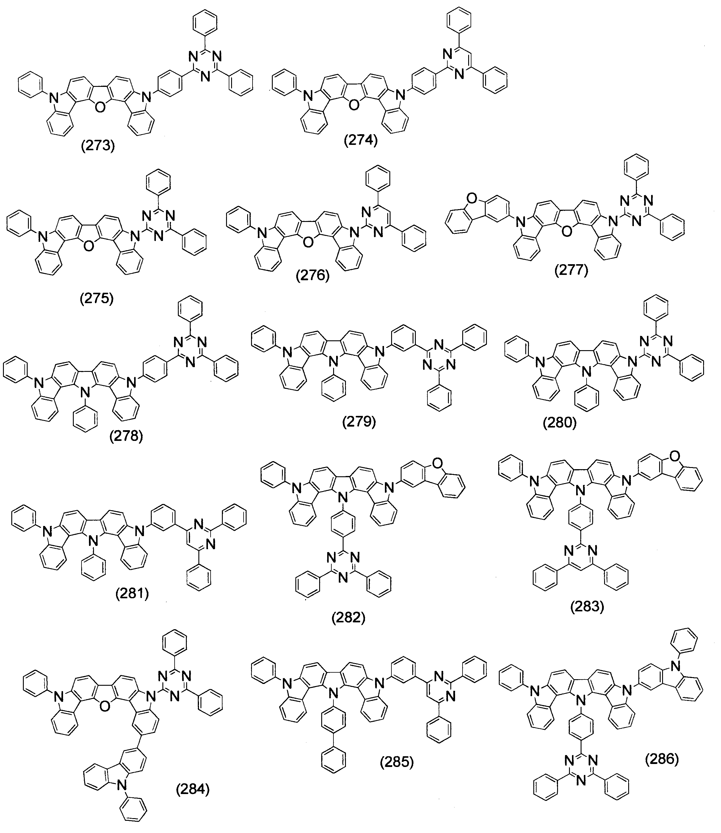
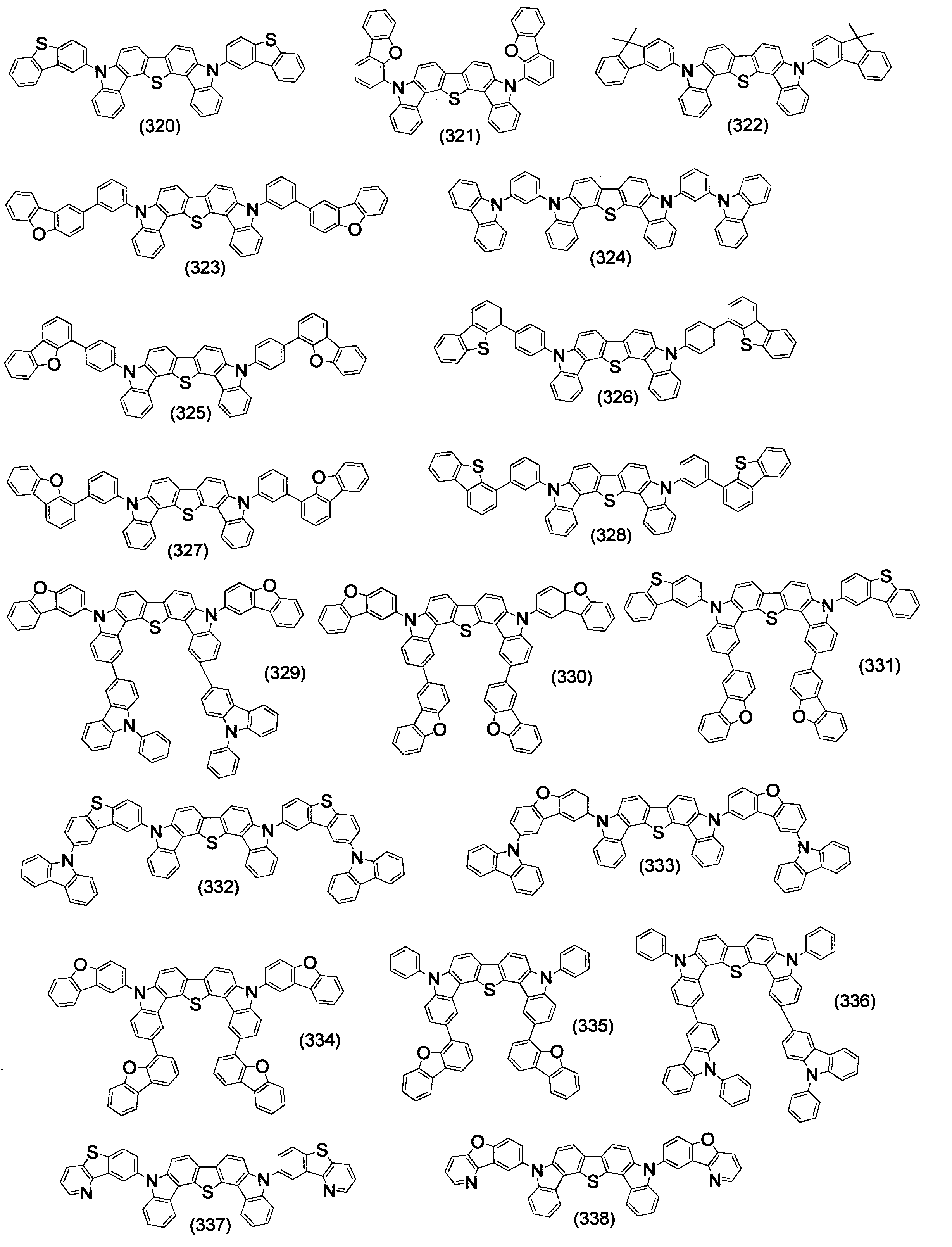
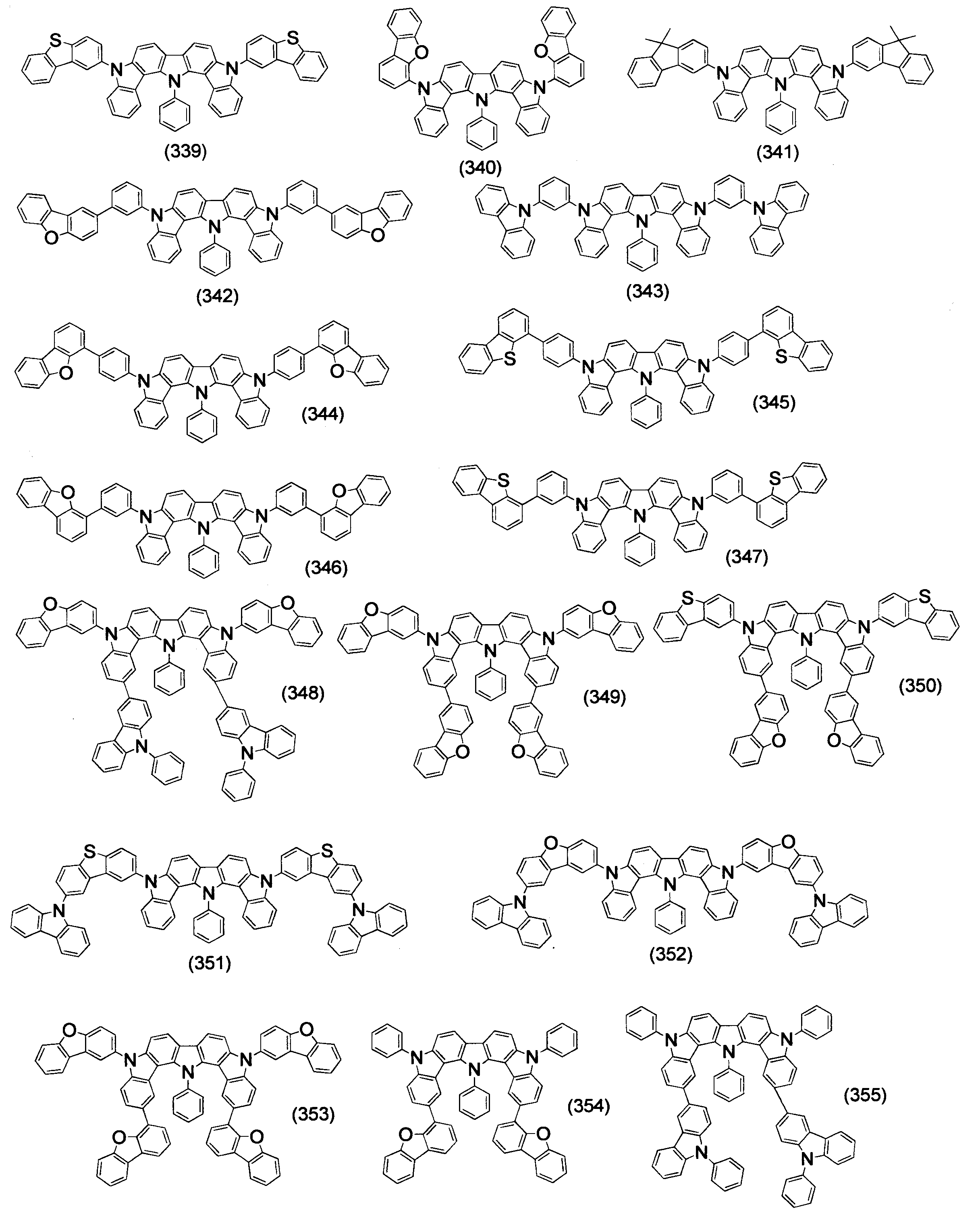
- the manufacturing method of the compound represented by Formula (1) of this invention is not specifically limited, It can manufacture by a well-known method. Specific examples of the compound represented by the formula (1) are shown below:
- the compound represented by Formula (1) of this invention can be used conveniently as an organic EL element material.
- the material for an organic EL element of the present invention contains a compound represented by the formula (1), preferably a light emitting layer material for an organic EL element, an electron barrier (blocking) layer material for an organic EL element, or a hole for an organic EL element. Used as a barrier (blocking) layer material, more preferably used as a light emitting layer material for an organic EL element and an electronic barrier (blocking) layer material for an organic EL element (collectively, hereinafter referred to as the organic EL element material of the present invention). Sometimes).
- the organic EL device material of the present invention may contain only the compound represented by the formula (1) of the present invention, and includes other materials in addition to the compound represented by the formula (1) of the present invention. You may go out.
- the hole transport material for organic EL devices of the present invention is a compound represented by the following formula (2) or formula (3).
- X is a group represented by O, S, or N-Ra.
- Y 1 to Y 12 are each a group represented by N or C—Ra.
- Two Ar 3 are the same substituted or unsubstituted heteroaryl group having 5 to 30 ring atoms.
- Ra represents a hydrogen atom, a deuterium atom, a substituent or an unsubstituted aryl group having 6 to 30 ring carbon atoms, a substituted or unsubstituted heteroaryl group having 5 to 30 ring atoms, a substituted or unsubstituted carbon.
- the plurality of Ras may be the same or different. However, Y 1 and Y 12 , Y 2 and Y 11 , Y 3 and Y 10 , Y 4 and Y 9 , Y 5 and Y 8 , and Y 6 and Y 7 are all the same group. )
- X, Y 1 to Y 12 and Ra in the formula (2) are the same as in the formula (1).
- Two Ar 3 in the formula (2) are the same substituted or unsubstituted heteroaryl group having 5 to 30 ring atoms, and this substituted or unsubstituted heteroaryl group having 5 to 30 ring atoms is The same as the substituted or unsubstituted heteroaryl group having 5 to 30 ring atoms in the formula (1).
- the heteroaryl group having 5 to 30 ring atoms of Ar 3 is preferably a nitrogen-containing heteroaryl group, an oxygen-containing heteroaryl group, or a sulfur-containing heteroaryl group, more preferably an oxygen-containing heteroaryl group, or It is a sulfur-containing heteroaryl group.
- X is a group represented by O, S, or N-Ra.
- Y 1 to Y 12 are each a group represented by N or C—Ra.
- Two Ar 4 groups are the same substituted or unsubstituted aryl group having 6 to 30 ring carbon atoms.
- Ra represents a hydrogen atom, a deuterium atom, a substituent or an unsubstituted aryl group having 6 to 30 ring carbon atoms, a substituted or unsubstituted heteroaryl group having 5 to 30 ring atoms, a substituted or unsubstituted carbon.
- the plurality of Ra may be the same or different.
- Y 1 and Y 12 , Y 2 and Y 11 , Y 3 and Y 10 , Y 4 and Y 9 , Y 5 and Y 8 , and Y 6 and Y 7 are all the same group.
- X, Y 1 to Y 12 and Ra in the formula (3) are the same as in the formula (1).
- Two Ar 4 of formula (3) has the same substituted or unsubstituted ring aryl group having 6 to 30, an aryl group of the substituted or unsubstituted ring carbon number of 6 to 30, wherein This is the same as the substituted or unsubstituted aryl group having 6 to 30 ring carbon atoms in (1).
- the aryl group having 6 to 30 ring carbon atoms of Ar 4 is preferably, for example, a phenyl group, a 9,9-dimethylfluorenyl group, a 9,9-diphenylfluorenyl group, a spirofluorenyl group, Examples include groups derived from a triphenylene ring. Examples of the aryl group having a substituent include a dibenzofuranylphenyl group and a dibenzofluorenylphenyl group.
- the organic EL element of the present invention will be described.
- the first organic EL device of the present invention has one or more organic thin film layers including a light emitting layer between an anode and a cathode. And at least 1 layer of an organic thin film layer contains the organic EL element material of this invention.
- One aspect of the first organic EL device of the present invention preferably has one or more organic thin film layers including a light emitting layer between the anode and the cathode, and the light emitting layer is a material for the organic EL device of the present invention. Containing.
- the organic EL element material containing the compound represented by the formula (1) is more preferably contained as a host material for the light emitting layer.
- one or more organic thin film layers including a light emitting layer are preferably provided between the anode and the cathode, and electrons adjacent to the light emitting layer between the anode and the light emitting layer. It has a barrier (blocking) layer, and the electron barrier (blocking) layer contains the organic EL device material of the present invention.
- One aspect of the second organic EL device of the present invention has one or more organic thin film layers including a light emitting layer between an anode and a cathode, and has a hole transport band between the anode and the light emitting layer.
- the hole transport zone contains a hole transport material for an organic electroluminescence device, which is a compound represented by the formula (2).
- Another aspect of the second organic EL device of the present invention has one or more organic thin film layers including a light emitting layer between an anode and a cathode, and a hole transport zone between the anode and the light emitting layer.
- a hole transport material for an organic electroluminescence device wherein the hole transport zone is a compound represented by the formula (3).
- FIG. 1 is a schematic view showing a layer structure of an embodiment of the organic EL device of the present invention.
- the organic EL element 1 has a configuration in which an anode 20, a hole transport zone 30, a phosphorescent light emitting layer 40, an electron transport zone 50, and a cathode 60 are laminated on a substrate 10 in this order.
- the hole transport zone 30 means a hole transport layer, a hole injection layer, an electron blocking layer, or the like.
- the electron transport zone 50 means an electron transport layer, an electron injection layer, a hole blocking layer, and the like. These need not be formed, but preferably one or more layers are formed.
- the organic thin film layer is each organic layer provided in the hole transport zone 30, each phosphor layer and the organic layer provided in the electron transport zone 50.
- at least one layer contains the organic EL device material of the present invention, or any one or more layers of the hole transport zone 30 contain the hole transport material for the organic EL device of the present invention.
- the content of the compound represented by the formula (1) with respect to the organic thin film layer containing the organic EL device material of the present invention is preferably 1 to 100% by weight.
- the content of the compound represented by formula (2) or formula (3) with respect to any layer in the hole transport zone containing the hole transport material for organic EL devices of the present invention is preferably 1 to 100. % By weight.
- the phosphorescent light emitting layer 40 preferably contains the organic EL device material of the present invention, and more preferably used as a host material of the light emitting layer. Since the organic EL device material of the present invention has sufficiently high triplet energy, even if a blue phosphorescent dopant material is used, the triplet energy of the phosphorescent dopant material is efficiently incorporated into the light emitting layer. Can be confined.
- the light emitting layer can be used not only for the blue light emitting layer but also for light emitting layers of longer wavelengths (such as green to red), but is preferably used for the blue light emitting layer.
- the phosphorescent light emitting layer contains a phosphorescent material (phosphorescent dopant).
- the phosphorescent material include metal complex compounds, preferably a compound having a metal atom selected from Ir, Pt, Os, Au, Cu, Re and Ru and a ligand.
- the ligand preferably has an ortho metal bond.
- the phosphorescent material is preferably a compound containing a metal atom selected from Ir, Os and Pt in that the phosphorescent quantum yield is high and the external quantum efficiency of the light-emitting element can be further improved.
- the phosphorescent material may be a single material or a mixture of two or more materials. Examples of the blue phosphorescent material include BD1 described later.
- the addition concentration of the phosphorescent material in the phosphorescent layer is not particularly limited, but is preferably 0.1 to 40% by weight (wt%), more preferably 0.1 to 30% by weight (wt%). is there.
- the organic EL element material of the present invention for the organic thin film layer adjacent to the phosphorescent light emitting layer 40.
- the layer functions as an electron barrier layer or excitons. It functions as a blocking layer.
- the barrier layer is a layer having a function of a carrier movement barrier or an exciton diffusion barrier.
- the organic layer for preventing electrons from leaking from the light-emitting layer to the hole transport zone is mainly defined as an electron barrier layer, and the organic layer for preventing holes from leaking from the light-emitting layer to the electron transport zone is defined as a hole barrier. Sometimes defined as a layer.
- an exciton blocking layer is an organic layer for preventing triplet excitons generated in the light emitting layer from diffusing into a peripheral layer having triplet energy lower than that of the light emitting layer. It may be defined as Further, the organic EL device material of the present invention can be used for an organic thin film layer adjacent to the phosphorescent light emitting layer 40 and further used for another organic thin film layer bonded to the adjacent organic thin film layer.
- the organic EL element of the present invention can employ various known configurations. Further, light emission of the light emitting layer can be taken out from the anode side, the cathode side, or both sides.
- an electron donating dopant and an organometallic complex is added to the interface region between the cathode and the organic thin film layer.
- the electron donating dopant include at least one selected from alkali metals, alkali metal compounds, alkaline earth metals, alkaline earth metal compounds, rare earth metals, rare earth metal compounds, and the like.
- the organometallic complex include at least one selected from an organometallic complex containing an alkali metal, an organometallic complex containing an alkaline earth metal, an organometallic complex containing a rare earth metal, and the like.
- alkali metal examples include lithium (Li) (work function: 2.93 eV), sodium (Na) (work function: 2.36 eV), potassium (K) (work function: 2.28 eV), rubidium (Rb) (work Function: 2.16 eV), cesium (Cs) (work function: 1.95 eV) and the like, and those having a work function of 2.9 eV or less are particularly preferable.
- K, Rb, and Cs are preferred, Rb and Cs are more preferred, and Cs is most preferred.
- alkaline earth metal examples include calcium (Ca) (work function: 2.9 eV), strontium (Sr) (work function: 2.0 eV to 2.5 eV), barium (Ba) (work function: 2.52 eV).
- a work function of 2.9 eV or less is particularly preferable.
- the rare earth metal examples include scandium (Sc), yttrium (Y), cerium (Ce), terbium (Tb), ytterbium (Yb) and the like, and those having a work function of 2.9 eV or less are particularly preferable.
- preferred metals are particularly high in reducing ability, and by adding a relatively small amount to the electron injection region, it is possible to improve the light emission luminance and extend the life of the organic EL element.
- alkali metal compound examples include lithium oxide (Li 2 O), cesium oxide (Cs 2 O), alkali oxides such as potassium oxide (K 2 O), lithium fluoride (LiF), sodium fluoride (NaF), fluorine.
- alkali halides such as cesium fluoride (CsF) and potassium fluoride (KF), and lithium fluoride (LiF), lithium oxide (Li 2 O), and sodium fluoride (NaF) are preferable.
- alkaline earth metal compound examples include barium oxide (BaO), strontium oxide (SrO), calcium oxide (CaO), and barium strontium oxide (Ba x Sr 1-x O) (0 ⁇ x ⁇ 1), Examples thereof include barium calcium oxide (Ba x Ca 1-x O) (0 ⁇ x ⁇ 1), and BaO, SrO, and CaO are preferable.
- the rare earth metal compound ytterbium fluoride (YbF 3), scandium fluoride (ScF 3), scandium oxide (ScO 3), yttrium oxide (Y 2 O 3), cerium oxide (Ce 2 O 3), gadolinium fluoride (GdF 3), include such terbium fluoride (TbF 3) is, YbF 3, ScF 3, TbF 3 are preferable.
- the organometallic complex is not particularly limited as long as it contains at least one of an alkali metal ion, an alkaline earth metal ion, and a rare earth metal ion as a metal ion as described above.
- the ligands include quinolinol, benzoquinolinol, acridinol, phenanthridinol, hydroxyphenyl oxazole, hydroxyphenyl thiazole, hydroxydiaryl thiadiazole, hydroxydiaryl thiadiazole, hydroxyphenylpyridine, hydroxyphenylbenzimidazole, hydroxybenzotriazole, Hydroxyfulborane, bipyridyl, phenanthroline, phthalocyanine, porphyrin, cyclopentadiene, ⁇ -diketones, azomethines, and derivatives thereof are preferred, but are not limited thereto.
- the electron donating dopant and the organometallic complex it is preferable to form a layer or an island in the interface region.
- a forming method while depositing at least one of an electron donating dopant and an organometallic complex by a resistance heating vapor deposition method, an organic material as a light emitting material or an electron injection material for forming an interface region is simultaneously deposited, and an electron is deposited in the organic material.
- a method of dispersing at least one of a donor dopant and an organometallic complex reducing dopant is preferable.
- the dispersion concentration is usually organic substance: electron donating dopant and / or organometallic complex in a molar ratio of 100: 1 to 1: 100, preferably 5: 1 to 1: 5.
- At least one of the electron donating dopant and the organometallic complex is formed in a layered form
- at least one of the electron donating dopant and the organometallic complex is formed.
- These are vapor-deposited by a resistance heating vapor deposition method alone, preferably with a layer thickness of 0.1 nm to 15 nm.
- an electron donating dopant and an organometallic complex is formed in an island shape
- a light emitting material or an electron injecting material which is an organic layer at the interface is formed in an island shape, and then the electron donating dopant and the organometallic complex are formed. At least one of them is vapor-deposited by a resistance heating vapor deposition method, preferably with an island thickness of 0.05 nm to 1 nm.
- the ratio of at least one of the main component (light-emitting material or electron injection material), the electron-donating dopant, and the organometallic complex is, as a molar ratio, the main component: the electron-donating dopant and / or
- the organometallic complex is preferably 5: 1 to 1: 5, more preferably 2: 1 to 1: 2.
- the configuration other than the layer using the organic EL element material of the present invention described above is not particularly limited, and a known material or the like can be used.
- a known material or the like can be used.
- the layer of a 1st element is demonstrated easily, the material applied to the 1st organic EL element of this invention is not limited to the following.
- a glass plate, a polymer plate or the like can be used as the substrate.
- the glass plate include soda lime glass, barium / strontium-containing glass, lead glass, aluminosilicate glass, borosilicate glass, barium borosilicate glass, and quartz.
- the polymer plate include polycarbonate, acrylic, polyethylene terephthalate, polyether sulfone, and polysulfone.
- the anode is made of, for example, a conductive material, and a conductive material having a work function larger than 4 eV is suitable.
- the conductive material include carbon, aluminum, vanadium, iron, cobalt, nickel, tungsten, silver, gold, platinum, palladium, and their alloys, ITO substrate, tin oxide used for NESA substrate, indium oxide, and the like. Examples thereof include metal oxides and organic conductive resins such as polythiophene and polypyrrole.
- the anode may be formed with a layer structure of two or more layers if necessary. When light emitted from the light emitting layer is extracted from the anode, the transmittance of the cathode for light emission is preferably greater than 10%.
- the cathode is made of, for example, a conductive material, and a conductive material having a work function smaller than 4 eV is suitable.
- the conductive material include, but are not limited to, magnesium, calcium, tin, lead, titanium, yttrium, lithium, ruthenium, manganese, aluminum, lithium fluoride, and alloys thereof.
- the alloy include magnesium / silver, magnesium / indium, lithium / aluminum, and the like, but are not limited thereto.
- the ratio of the alloy is controlled by the temperature of the vapor deposition source, the atmosphere, the degree of vacuum, etc., and is selected to an appropriate ratio.
- the cathode may be formed with a layer structure of two or more layers, and the cathode can be produced by forming a thin film from the conductive material by a method such as vapor deposition or sputtering.
- the transmittance of the cathode for light emission is preferably greater than 10%.
- the sheet resistance as the cathode is preferably several hundred ⁇ / ⁇ or less, and the film thickness is usually 10 nm to 1 ⁇ m, preferably 50 to 200 nm.
- the phosphorescent light emitting layer is formed of a material other than the organic EL element material of the present invention
- a known material can be used as the material of the phosphorescent light emitting layer.
- Japanese Patent Application No. 2005-517938 may be referred to.
- the 1st organic EL element of this invention may have the fluorescence light emitting layer 70 like the element shown in FIG.
- known materials can be used in addition to the organic EL device material of the present invention.
- the light emitting layer may be a double host (also referred to as a host / cohost) using two types of host materials. Specifically, the carrier balance in the light emitting layer may be adjusted by combining an electron transporting host and a hole transporting host in the light emitting layer.
- the material for an organic EL device of the present invention can be used as a host or a cohost. Moreover, it is good also as a double dopant using two types of luminescent materials (dopant material).
- each dopant emits light by adding two or more dopant materials having a high quantum yield. For example, a yellow light emitting layer may be realized by co-evaporating a host, a red dopant, and a green dopant.
- the light emitting layer may be a single layer or a laminated structure.
- the recombination region may be concentrated on the light emitting layer interface by accumulating electrons and holes at the light emitting layer interface. In such a case, quantum efficiency is improved.
- the hole injection / transport layer is a layer that assists hole injection into the light emitting layer and transports it to the light emitting region, and has a high hole mobility and a low ionization energy.
- the hole injection / transport layer may have a single layer structure or a multilayer structure in which a hole injection layer and a hole transport layer are stacked. Furthermore, the hole injection layer may have a multilayer structure, and the hole transport layer may have a multilayer structure.
- the layer in contact with the light emitting layer may be an electron barrier (blocking) layer.
- the electron barrier (blocking) material a material containing the organic EL element material of the present invention can be used.
- the material for the hole injection / transport layer a material that transports holes to the light emitting layer with lower electric field strength is preferable. Further, when an electric field is applied with a hole mobility of, for example, 10 4 to 10 6 V / cm, At least 10 ⁇ 4 cm 2 / V ⁇ sec is preferable.
- the material for the hole injection / transport layer include triazole derivatives (see US Pat. No. 3,112,197) and oxadiazole derivatives (see US Pat. No. 3,189,447). ), Imidazole derivatives (see JP-B-37-16096, etc.), polyarylalkane derivatives (US Pat. Nos. 3,615,402, 3,820,989, 3,542,544) Nos. 45-555, 51-10983, 51-93224, 55-17105, 56-4148, 55-108667, 55-156953, 56-36656, etc.), pyrazoline derivatives and pyrazolone derivatives (US Pat. No. 3,180,729, No. 4) Nos.
- Gazette 55-52063, 55-52064, 55-46760, 57-11350, 57- No. 148749, JP-A-2-311591, etc.), stilbene derivatives (JP-A Nos. 61-210363, 61-228451, 61-14642, 61-72255, etc.) 62-47646, 62-36684, 62-10652, 62-30255, 60-93455, 60-94462, 60-174749, 60 -175052, etc.), silazane derivatives (US Pat. No. 4,950,950), polysilanes (JP-A-2-204996), aniline copolymers (JP-A-2-282263) Etc.
- inorganic compounds such as p-type Si and p-type SiC can also be used as the hole injection material.
- a cross-linkable material can be used as the material for the hole injection / transport layer.
- Mater. 2008, 20, 413-422, Chem. Mater. Examples include a layer obtained by insolubilizing a cross-linking material such as 2011, 23 (3), 658-681, WO2008108430, WO2009102027, WO2009123269, WO2010016555, WO2010018813 by heat, light or the like.
- the electron injection / transport layer is a layer that assists the injection of electrons into the light emitting layer and transports it to the light emitting region, and has a high electron mobility.
- the electron injection / transport layer may have a single layer structure or a multilayer structure in which an electron injection layer and an electron transport layer are stacked. Furthermore, the electron injection layer may have a multilayer structure, and the electron transport layer may have a multilayer structure.
- the layer in contact with the light emitting layer may be a hole blocking (blocking) layer.
- a known material can be used as the hole blocking (blocking) material. Examples thereof include the compound (H1) used in Example 2 described later.
- the electron injecting / transporting layer is appropriately selected with a film thickness of several nm to several ⁇ m. However, particularly when the film thickness is large, in order to avoid a voltage increase, 10 4 to 10 6.
- the electron mobility is preferably at least 10 ⁇ 5 cm 2 / Vs or more when an electric field of V / cm is applied.
- an aromatic heterocyclic compound containing one or more heteroatoms in the molecule is preferably used, and a nitrogen-containing ring derivative is particularly preferable.
- the nitrogen-containing ring derivative is preferably an aromatic ring having a nitrogen-containing 6-membered ring or 5-membered ring skeleton, or a condensed aromatic ring compound having a nitrogen-containing 6-membered ring or 5-membered ring skeleton, such as a pyridine ring. , Pyrimidine ring, triazine ring, benzimidazole ring, phenanthroline ring, quinazoline ring and the like.
- an organic layer having semiconductivity may be formed by doping a donor material (n) and acceptor material (p).
- a donor material (n) and acceptor material (p) may be doped by doping a donor material (n) and acceptor material (p).
- N doping is to dope a metal such as Li or Cs into an electron transporting material
- P doping is to dope an acceptor material such as F4TCNQ into a hole transporting material (for example, see Japanese Patent No. 3695714).
- each layer of the organic EL device of the present invention a known method such as a dry film forming method such as vacuum deposition, sputtering, plasma, or ion plating, or a wet film forming method such as spin coating, dipping, or flow coating is applied. be able to.
- the thickness of each layer is not particularly limited, but must be set to an appropriate thickness. If the film thickness is too thick, a large applied voltage is required to obtain a constant light output, resulting in poor efficiency. If the film thickness is too thin, pinholes and the like are generated, and sufficient light emission luminance cannot be obtained even when an electric field is applied.
- the normal film thickness is suitably in the range of 5 nm to 10 ⁇ m, but more preferably in the range of 10 nm to 0.2 ⁇ m.
- the 2nd organic EL element of this invention it is not specifically limited about structures other than the layer using the hole transport material for organic EL elements of this invention mentioned above, A well-known material etc. can be used.
- the material applied to the 2nd organic EL element of this invention is not limited to the following.
- the substrate, the anode, the cathode, the electron injection layer, and the electron transport layer constituting the organic EL element are the same as those of the first organic EL element described above.
- the light emitting layer is the same as the first organic EL element described above, but the material for the organic EL element of the present invention is not necessarily used.
- the organic EL element material of the present invention is used for the light emitting layer.
- the hole injection layer and the hole transport layer are also the same as the first organic EL element described above, but the hole transport material for the organic EL element of the present invention is used as a hole transport layer, a hole injection layer, or an electron blocking layer. It is necessary to use any one of these.
- Example 1 Synthesis of Compound (7) (1) Synthesis of compound (7-a) A three-necked flask was charged with 20.0 g (80.9 mmol) of dibenzofuran and 200 ml of dehydrated tetrahydrofuran, and the reactor was cooled to ⁇ 70 ° C. in a nitrogen atmosphere. To the reactor, 53 ml (88.9 mmol) of a 1.68M s-butyllithium hexane solution was added dropwise and stirred at -70 ° C. for 1 hour. To this, 37.3 ml (162 mmol) of triisopropyl borate was further added and stirred at room temperature for 6 hours.
- Example 2 A glass substrate with a 130 nm-thick ITO electrode line (manufactured by Geomatic) was ultrasonically cleaned in isopropyl alcohol for 5 minutes, followed by UV ozone cleaning for 30 minutes. The glass substrate with the ITO electrode line after the cleaning is mounted on the substrate holder of the vacuum deposition apparatus, and the compound (HI1) is first thickened so as to cover the ITO electrode line on the surface on which the ITO electrode line is formed. The compound (HT1) was deposited by resistance heating at a thickness of 60 nm at a thickness of 20 nm, and thin films were sequentially formed. The film formation rate was 1 ⁇ / s.
- These thin films function as a hole injection layer and a hole transport layer, respectively.
- the compound (7) and the compound (BD1) were simultaneously deposited by resistance heating to form a thin film having a thickness of 50 nm.
- the compound (BD1) was deposited so as to have a mass ratio of 20% with respect to the total mass of the compound (7) and the compound (BD1).
- the film formation rates were 1.2 ⁇ / s and 0.3 ⁇ / s, respectively.
- This thin film functions as a phosphorescent light emitting layer.
- a thin film having a thickness of 10 nm was formed on the phosphorescent light emitting layer by resistance heating vapor deposition of the compound (H1).
- the film formation rate was 1.2 liter / s. This thin film functions as a barrier layer.
- a thin film having a thickness of 10 nm was formed on this barrier layer by resistance heating vapor deposition of the compound (ET1).
- the film formation rate was 1 ⁇ / s.
- This film functions as an electron injection layer.
- LiF having a film thickness of 1.0 nm was deposited on the electron injection layer at a film formation rate of 0.1 ⁇ / s.
- metal aluminum was vapor-deposited on the LiF film at a film formation rate of 8.0 ⁇ / s to form a metal cathode having a film thickness of 80 nm, thereby manufacturing an organic EL element.
- Comparative Example 1 An organic EL device was prepared and evaluated in the same manner as in Example 1 except that the compound (H2) was used instead of the compound (7) as the phosphorescent host material. The results are shown in Table 1.
- the organic EL device of Example 2 using the compound of the present invention of Example 1 for the light emitting layer has improved luminous efficiency compared to the device of Comparative Example 1.
- the emission wavelength of the organic EL element of Example 2 was 475 nm.
- Example 3 Synthesis of Compound (40) (1) Synthesis of compound (40-a) In a reaction vessel, 34.6 g (100 mmol) of compound (7-c), 24.7 g (100 mmol) of 2-bromodibenzofuran, 19.0 g (100 mmol) of copper iodide, 21.2 g (100 mmol) of tripotassium phosphate, cyclohexanediamine 5.9 g (50 mmol) and dehydrated 1,4-dioxane 500 mL were added and refluxed for 48 hours under an argon atmosphere.
- Example 4 Synthesis of Compound (41)
- a reaction vessel 3.5 g (10 mmol) of compound (40-a), 3.6 g (11 mmol) of 3-bromo-9-phenylcarbazole, 1.9 g (10 mmol) of copper iodide, 2.1 g (10 mmol) of tripotassium phosphate ), 0.6 g (5 mmol) of cyclohexanediamine and 50 mL of dehydrated 1,4-dioxane were added and refluxed for 40 hours under an argon atmosphere.
- the reaction product was filtered through Celite, transferred to a separatory funnel, and extracted several times with dichloromethane.
- Example 5 Synthesis of Compound (42)
- a reaction vessel 3.5 g (10 mmol) of compound (40-a), 3.0 g (12 mmol) of intermediate (A) synthesized by the method described in WO2013-038650, 1.9 g (10 mmol) of copper iodide, Tripotassium phosphate (2.1 g, 10 mmol), cyclohexanediamine (1.2 g, 10 mmol) and dehydrated 1,4-dioxane (40 mL) were added, and the mixture was refluxed for 72 hours under an argon atmosphere.
- Tripotassium phosphate 2.1 g, 10 mmol
- cyclohexanediamine 1.2 g, 10 mmol
- dehydrated 1,4-dioxane 40 mL
- Example 6 Synthesis of Compound (51)
- Compound (51) was synthesized according to the method described in Example 1 by using dibenzothiophene instead of dibenzofuran as a starting material.
- Example 7 (Synthesis of Compound (128)) (1) Synthesis of compound (128-a) In a reaction vessel, 24.9 g (100 mmol) of 2-iodonitrobenzene, 20.0 g (100 mmol) of 2-bromophenylboronic acid, 2.3 g (2 mmol) of Pd (PPh 3 ) 4 , 2OmM sodium carbonate aqueous solution 100 mL, toluene 150 mL, 1 , 2-Dimethoxyethane (DME) (150 mL) was added, and the mixture was refluxed for 24 hours under an argon atmosphere.
- DME 2-Dimethoxyethane
- Example 8 An organic EL device was produced in the same manner as in Example 2 except that the compound (H3) was used instead of the compound (H1). The produced organic EL element was made to emit light by direct current drive, the luminance and current density were measured, and the voltage and luminous efficiency (external quantum efficiency) at a current density of 1 mA / cm 2 were obtained. Furthermore, the 70% luminance lifetime (the time during which the luminance decreases to 70%) at an initial luminance of 3,000 cd / m 2 is described as a relative value when the element of the comparative example is taken as 100. Table 2 shows the evaluation results of these light emission performances.
- Examples 9-21 An organic EL device was prepared and evaluated in the same manner as in Example 8 except that the compounds shown in Table 2 were used instead of the compound (7) as the phosphorescent host material. The results are shown in Table 2.
- Comparative Example 2 An organic EL device was prepared and evaluated in the same manner as in Example 8 except that the compound (H2) was used instead of the compound (7) as the phosphorescent host material. The results are shown in Table 2.
- Comparative Example 3 An organic EL device was prepared and evaluated in the same manner as in Example 8 except that the compound (H4) was used instead of the compound (7) as the phosphorescent host material. The results are shown in Table 2.
- Comparative Example 4 An organic EL device was prepared and evaluated in the same manner as in Example 8 except that the compound (H5) was used instead of the compound (7) as the phosphorescent host material. The results are shown in Table 2.
- the organic EL devices using the compounds of the present invention of Examples 8 to 21 as the phosphorescent host material in the light emitting layer have lower voltage and longer life than the comparative devices, and the luminous efficiency.
- the compound of the present invention having no symmetry axis has higher performance as a material for organic EL devices than the comparative compound having the symmetry axis.
- the compound of the present invention can be used as a material for an organic EL device.
- the organic EL device of the present invention can be used for a flat light emitter such as a flat panel display of a wall-mounted television, a light source such as a copying machine, a printer, a backlight of a liquid crystal display or instruments, a display board, a marker lamp, and the like.
Landscapes
- Chemical & Material Sciences (AREA)
- Organic Chemistry (AREA)
- Engineering & Computer Science (AREA)
- Materials Engineering (AREA)
- Physics & Mathematics (AREA)
- Spectroscopy & Molecular Physics (AREA)
- Crystallography & Structural Chemistry (AREA)
- Inorganic Chemistry (AREA)
- Electroluminescent Light Sources (AREA)
- Nitrogen Condensed Heterocyclic Rings (AREA)
- Heterocyclic Carbon Compounds Containing A Hetero Ring Having Oxygen Or Sulfur (AREA)
- Nitrogen And Oxygen Or Sulfur-Condensed Heterocyclic Ring Systems (AREA)
Abstract
Description
燐光発光は、三重項励起子を利用した発光であるため、発光層に用いる化合物のエネルギーギャップが大きくなくてはならない。これは、ある化合物のエネルギーギャップ(以下、一重項エネルギーともいう。)の値は、通常、その化合物の三重項エネルギー(本発明では、最低励起三重項状態と基底状態とのエネルギー差をいう。)の値よりも大きいからである。
燐光型の有機EL素子の材料として、例えば特許文献1は、線対称構造を有するりん光ホスト材料を開示する。
1.下記式(1)で表わされる化合物。

Xは、O、S、又はN-Raで表わされる基である。
Y1~Y12は、それぞれN又はC-Raで表わされる基である。
Ar1及びAr2は、それぞれ置換若しくは無置換の環形成炭素数6~30のアリール基、又は、置換若しくは無置換の環形成原子数5~30のヘテロアリール基である。
Raは、水素原子、重水素原子、置換基若しくは無置換の環形成炭素数6~30のアリール基、置換若しくは無置換の環形成原子数5~30のヘテロアリール基、置換若しくは無置換の炭素数1~30のアルキル基、置換若しくは無置換の炭素数1~30のフルオロアルキル基、置換若しくは無置換の環形成炭素数3~30のシクロアルキル基、置換若しくは無置換の炭素数7~30のアラルキル基、置換ホスホリル基、置換シリル基、置換ゲルマニウム基、シアノ基、ニトロ基、又はカルボキシ基である。
式(1)中に、Raが2つ以上ある場合は、複数のRaは、それぞれ同一でも異なっていてもよい。
但し、Ar1とAr2が同一の置換基である場合、Y1とY12、Y2とY11、Y3とY10、Y4とY9、Y5とY8、及びY6とY7の全てが、それぞれ互いに同じ基とはならない。)
2.前記式(1)のAr1及びAr2が、それぞれ置換若しくは無置換の環形成炭素数6~30のアリール基である1に記載の化合物。
3.前記式(1)のAr1及びAr2が、それぞれ置換若しくは無置換の環形成原子数5~30のヘテロアリール基である1に記載の化合物。
4.前記式(1)のXが、N-Raで表わされる基である1~3のいずれかに記載の化合物。
5.前記式(1)のXが、O又はSである1~3のいずれかに記載の化合物。
6.前記式(1)のY1~Y12が、それぞれC-Raで表わされる基である1~5のいずれかに記載の化合物。
7.前記式(1)のAr1が、-L1-R1で表される1~6のいずれかに記載の化合物。
(L1は、置換若しくは無置換の環形成炭素数6~30のアリーレン基、又は、置換若しくは無置換の環形成原子数5~30のヘテロアリーレン基を表し、R1は、置換若しくは無置換の環形成炭素数6~30のアリール基、又は、置換若しくは無置換の環形成原子数5~30のヘテロアリール基を表す。)
8.L1が、置換若しくは無置換の環形成炭素数6~30のアリーレン基を表す7に記載の化合物。
9.L1が、置換若しくは無置換の環形成原子数5~30のヘテロアリーレン基を表す7に記載の化合物。
10.1~9のいずれかに記載の化合物を含む有機エレクトロルミネッセンス素子用材料。
11.下記式(2)で表わされる有機エレクトロルミネッセンス素子用正孔輸送材料。

Xは、O、S、又はN-Raで表わされる基である。
Y1~Y12は、それぞれN又はC-Raで表わされる基である。
2つのAr3は、同一の置換若しくは無置換の環形成原子数5~30のヘテロアリール基である。
Raは、水素原子、重水素原子、置換基若しくは無置換の環形成炭素数6~30のアリール基、置換若しくは無置換の環形成原子数5~30のヘテロアリール基、置換若しくは無置換の炭素数1~30のアルキル基、置換若しくは無置換の炭素数1~30のフルオロアルキル基、置換若しくは無置換の環形成炭素数3~30のシクロアルキル基、置換若しくは無置換の炭素数7~30のアラルキル基、置換ホスホリル基、置換シリル基、シアノ基、ニトロ基、又はカルボキシ基である。
式(2)中に、Raが2つ以上ある場合は、複数のRaは、それぞれ同一でも異なっていてもよい。
但し、Y1とY12、Y2とY11、Y3とY10、Y4とY9、Y5とY8、及びY6とY7の全てが、それぞれ互いに同じ基である。)
12.下記式(3)で表わされる有機エレクトロルミネッセンス素子用正孔輸送材料。
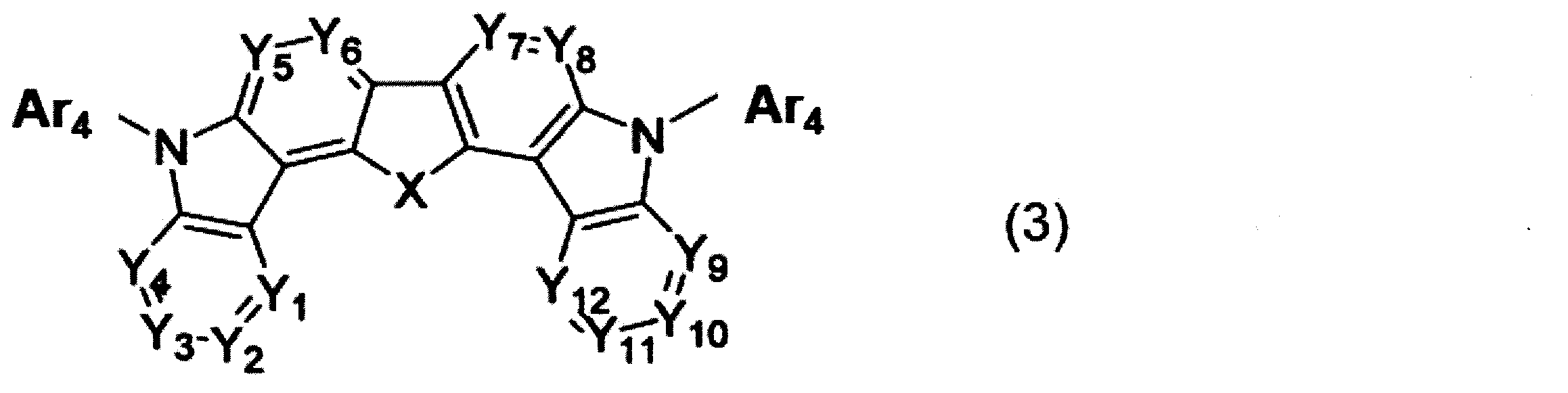
Xは、O、S、又はN-Raで表わされる基である。
Y1~Y12は、それぞれN又はC-Raで表わされる基である。
2つのAr4は、同一の置換若しくは無置換の環形成炭素数6~30のアリール基である。
Raは、水素原子、重水素原子、置換基若しくは無置換の環形成炭素数6~30のアリール基、置換若しくは無置換の環形成原子数5~30のヘテロアリール基、置換若しくは無置換の炭素数1~30のアルキル基、置換若しくは無置換の炭素数1~30のフルオロアルキル基、置換若しくは無置換の環形成炭素数3~30のシクロアルキル基、置換若しくは無置換の炭素数7~30のアラルキル基、置換ホスホリル基、置換シリル基、シアノ基、ニトロ基、又はカルボキシ基である。
式(3)中に、Raが2つ以上ある場合は、複数のRaは、それぞれ同一でも異なっていてもよい。
但し、Y1とY12、Y2とY11、Y3とY10、Y4とY9、Y5とY8、及びY6とY7の全てが、それぞれ互いに同じ基である。)
13.陽極と陰極の間に、発光層を含む1層以上の有機薄膜層を有し、前記有機薄膜層の少なくとも1層が10に記載の有機エレクトロルミネッセンス素子用材料を含有する有機エレクトロルミネッセンス素子。
14.前記発光層が前記有機エレクトロルミネッセンス素子用材料を含む13に記載の有機エレクトロルミネッセンス素子。
15.前記陰極と前記発光層の間に電子輸送帯域を有し、該電子輸送帯域が前記有機エレクトロルミネッセンス素子用材料を含む14に記載の有機エレクトロルミネッセンス素子。
16.陽極と陰極の間に、発光層を含む1層以上の有機薄膜層を有し、
前記陽極と前記発光層の間に正孔輸送帯域を有し、該正孔輸送帯域が11に記載の有機エレクトロルミネッセンス素子用正孔輸送材料を含有する有機エレクトロルミネッセンス素子。
17.陽極と陰極の間に、発光層を含む1層以上の有機薄膜層を有し、
前記陽極と前記発光層の間に正孔輸送帯域を有し、該正孔輸送帯域が12に記載の有機エレクトロルミネッセンス素子用正孔輸送材料を含有する有機エレクトロルミネッセンス素子。
18.前記発光層が燐光発光材料を含有し、前記燐光発光材料がイリジウム(Ir)、オスミウム(Os)及び白金(Pt)から選択される金属原子のオルトメタル化錯体である13~17のいずれかに記載の有機エレクトロルミネッセンス素子。
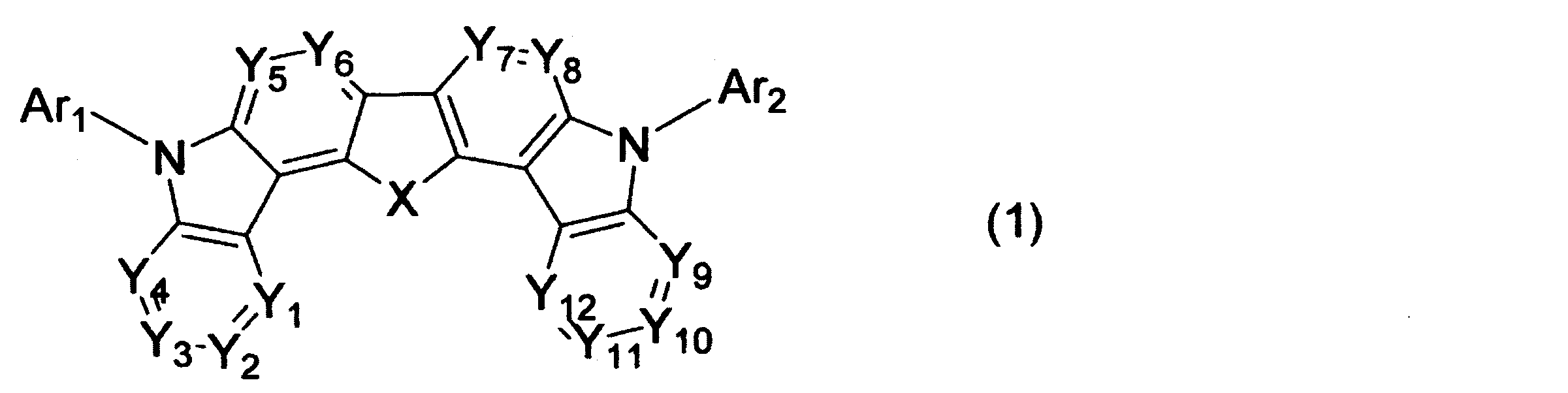
Xは、O、S、又はN-Raで表わされる基である。
Y1~Y12は、それぞれN又はC-Raで表わされる基である。
Ar1及びAr2は、それぞれ置換若しくは無置換の環形成炭素数6~30のアリール基、又は、置換若しくは無置換の環形成原子数5~30のヘテロアリール基である。
Raは、水素原子、重水素原子、置換基若しくは無置換の環形成炭素数6~30のアリール基、置換若しくは無置換の環形成原子数5~30のヘテロアリール基、置換若しくは無置換の炭素数1~30のアルキル基、置換若しくは無置換の炭素数1~30のフルオロアルキル基、置換若しくは無置換の環形成炭素数3~30のシクロアルキル基、置換若しくは無置換の炭素数7~30のアラルキル基、置換ホスホリル基、置換シリル基、置換ゲルマニウム基、シアノ基、ニトロ基、又はカルボキシ基である。
式(1)中に、Raが2つ以上ある場合は、複数のRaは、それぞれ同一でも異なっていてもよい。
但し、Ar1とAr2が同一の置換基である場合、Y1とY12、Y2とY11、Y3とY10、Y4とY9、Y5とY8、及びY6とY7の全てが、それぞれ互いに同じ基とはならない。)
キャリア輸送性に優れる本発明の化合物を、有機EL素子の材料として用いることで、素子内のキャリアバランスを整え、素子を高効率化させることができる。
また、式(1)を構成する2つのカルバゾリル基の3,4位でヘテロ原子Xを含む構造と結合し、ラダー構造を形成していることが、三重項エネルギーの大きな化合物を得ることに寄与している。
本発明の化合物は、Ar1とAr2が異なる置換基である方が好ましい。ここで、Ar1とAr2が同一の基であっても、ラダー構造と結合する位置が異なる場合は、線対称構造を取らないため、異なる置換基である。このような例として、例えば、Ar1とAr2を構成する2個のジベンゾフラニル基の一方が2位でラダー構造と結合し、他方が4位で結合する構造である。しかしながら、ラダー構造と結合する前の構造が異なる基の方が好ましい。
本発明の化合物が非対称構造化合物であることで、結晶性が低減し、アモルファスな有機膜を維持することで、適切な電荷輸送を維持することができる。
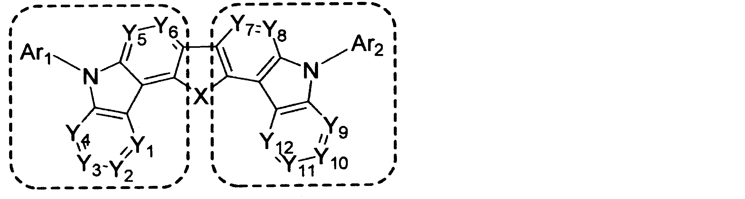
一の態様において、Ar1は、-L1-R1で表される。L1は、置換若しくは無置換の環形成炭素数6~30のアリーレン基、又は、置換若しくは無置換の環形成原子数5~30のヘテロアリーレン基を表し、R1は、置換若しくは無置換の環形成炭素数6~30のアリール基、又は、置換若しくは無置換の環形成原子数5~30のヘテロアリール基を表す。
Y1~Y12は、長寿命化の点で好ましくはそれぞれC-Raで表わされる基である。更に好ましくは、-CHである。Y1~Y12の隣接する基がC-Ra(-CHでもよい。)の場合、この隣接する基が結合して環を形成しても良い。π共役平面の広がりの維持という点では、隣接する基が結合して形成する環は芳香族環が好ましい。この場合、環形成原子として、N,O,Sのようなヘテロ原子を含む芳香族環でもよい。一方、蒸着法を用いて式(1)の化合物の有機薄膜を形成して有機EL素子を製造する場合には、式(1)に示すような7つの環でラダーを形成する化合物が好ましい。
炭素数1~30のアルキル基としては、直鎖状若しくは分岐状のアルキル基があり、具体的には、メチル基、エチル基、プロピル基、イソプロピル基、n-ブチル基、イソブチル基、sec-ブチル基、tert-ブチル基、n-ペンチル基、n-ヘキシル基、n-ヘプチル基、n-オクチル基等が挙げられ、好ましくは、メチル基、エチル基、プロピル基、イソプロピル基、n-ブチル基、イソブチル基、sec-ブチル基、tert-ブチル基が挙げられ、より好ましくはメチル基、エチル基、プロピル基、イソプロピル基、n-ブチル基、sec-ブチル基、tert-ブチル基である。
尚、「環形成炭素」とは飽和環、不飽和環、又は芳香環を構成する炭素原子を意味する。
アリール基の具体例としては、フェニル基、ナフチル基、アントリル基、フェナントリル基、ナフタセニル基、ピレニル基、クリセニル基、ベンゾ[c]フェナントリル基、ベンゾ[g]クリセニル基、トリフェニレニル基、フルオレニル基、ベンゾフルオレニル基、ジベンゾフルオレニル基、ビフェニルイル基、ターフェニル基、クォーターフェニル基、フルオランテニル基等が挙げられ、好ましくはナフチル基、アントリル基、フェナントリル基、ナフタセニル基、ピレニル基、クリセニル基である。
環形成炭素数6~30のアリーレン基は、好ましくは環形成炭素数6~20のアリーレン基である。具体例としては、上記のアリール基における2価の基が挙げられる。
ヘテロアリール基の具体例としては、ピロリル基、ピラジニル基、ピリジニル基、ピリミジニル基、トリアジニル基、インドリル基、イソインドリル基、イミダゾリル基、フリル基、ベンゾフラニル基、イソベンゾフラニル基、ジベンゾフラニル基、ジベンゾチオフェニル基、アザジベンゾフラニル基、アザジベンゾチオフェニル基、ジアザジベンゾフラニル基、ジアザジベンゾチオフェニル基、キノリル基、イソキノリル基、キノキサリニル基、カルバゾリル基、フェナントリジニル基、アクリジニル基、フェナントロリニル基、フェナジニル基、フェノチアジニル基、フェノキサジニル基、オキサゾリル基、オキサジアゾリル基、フラザニル基、チエニル基、ベンゾチオフェニル基、ジヒドロアクリジニル基、アザカルバゾリル基、ジアザカルバゾリル基、キナゾリニル基等が挙げられ、好ましくは、ピリジニル基、ピリミジニル基、トリアジニル基、ジベンゾフラニル基、ジベンゾチオフェニル基、アザジベンゾフラニル基、アザジベンゾチオフェニル基、ジアザジベンゾフラニル基、ジアザジベンゾチオフェニル基、カルバゾリル基、アザカルバゾリル基、ジアザカルバゾリル基である。
式(1)で表される化合物を青色燐光発光有機EL素子に使用する場合は、ジベンゾフラニル基、ジベンゾチオフェニル基、アザジベンゾフラニル基、アザジベンゾチオフェニル基、ジアザジベンゾフラニル基、ジアザジベンゾチオフェニル基、カルバゾリル基、アザカルバゾリル基、ジアザカルバゾリル基が好ましい。
環形成原子数5~30のヘテロアリーレン基としては、具体的には、上記のヘテロアリール基における2価の基が挙げられる。
アラルキル基のアリール部分は、環形成炭素数が6~20が好ましい。アルキル部分は炭素数1~8が好ましい。アラルキル基としては、例えば、ベンジル基、フェニルエチル基、2-フェニルプロパン-2-イル基である。
置換ゲルマニウム基は、例えば、-GeRbRcRdで表される基である。
Rb、Rc及びRdは、それぞれ置換若しくは無置換の環形成炭素数6~30のアリール基、置換若しくは無置換の環形成原子数5~30のヘテロアリール基、置換若しくは無置換の炭素数1~30のアルキル基、置換若しくは無置換の炭素数1~30のフルオロアルキル基、又は置換若しくは無置換の環形成炭素数3~30のシクロアルキル基である。
これらRb、Rc及びRdの各基は、上述したものと同じである。
以下に、式(1)で表わされる化合物の具体例を示す:
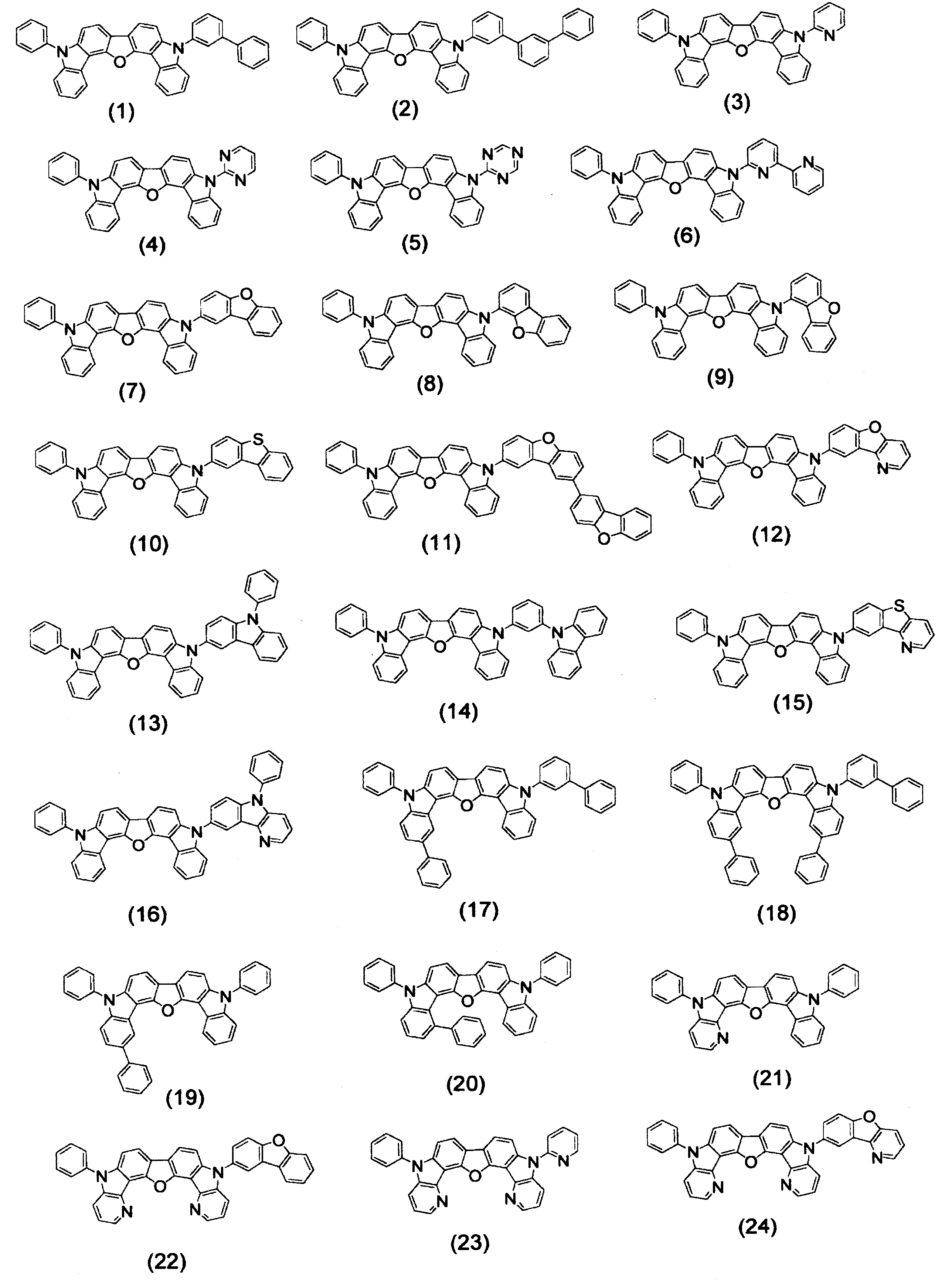
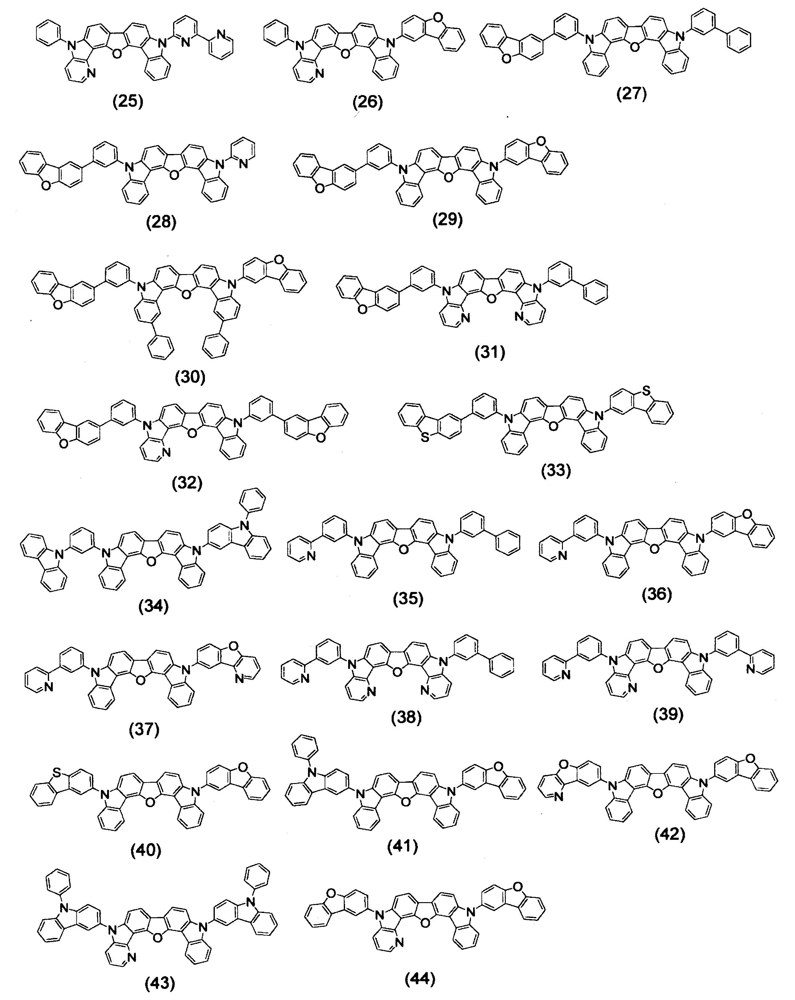
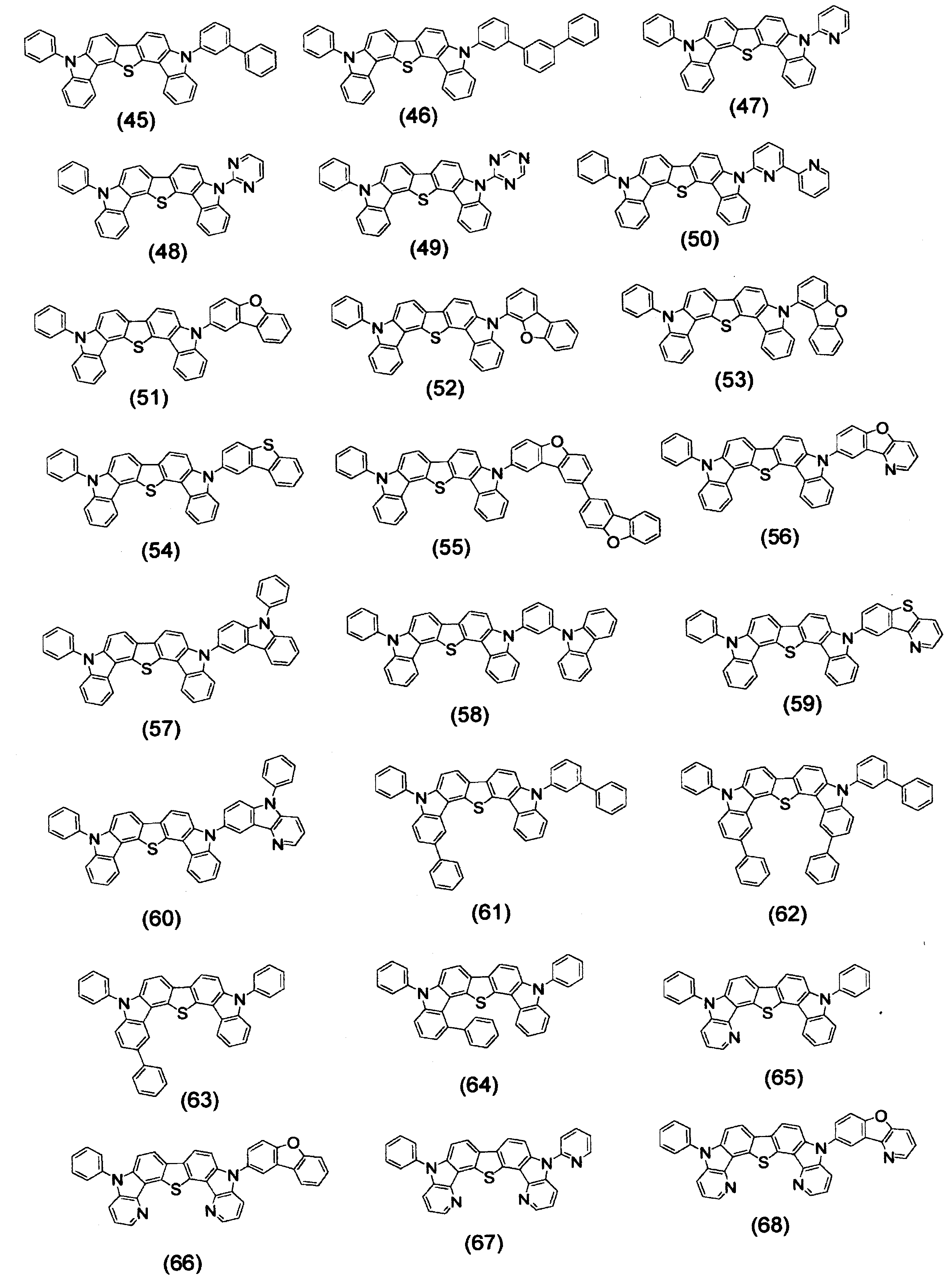
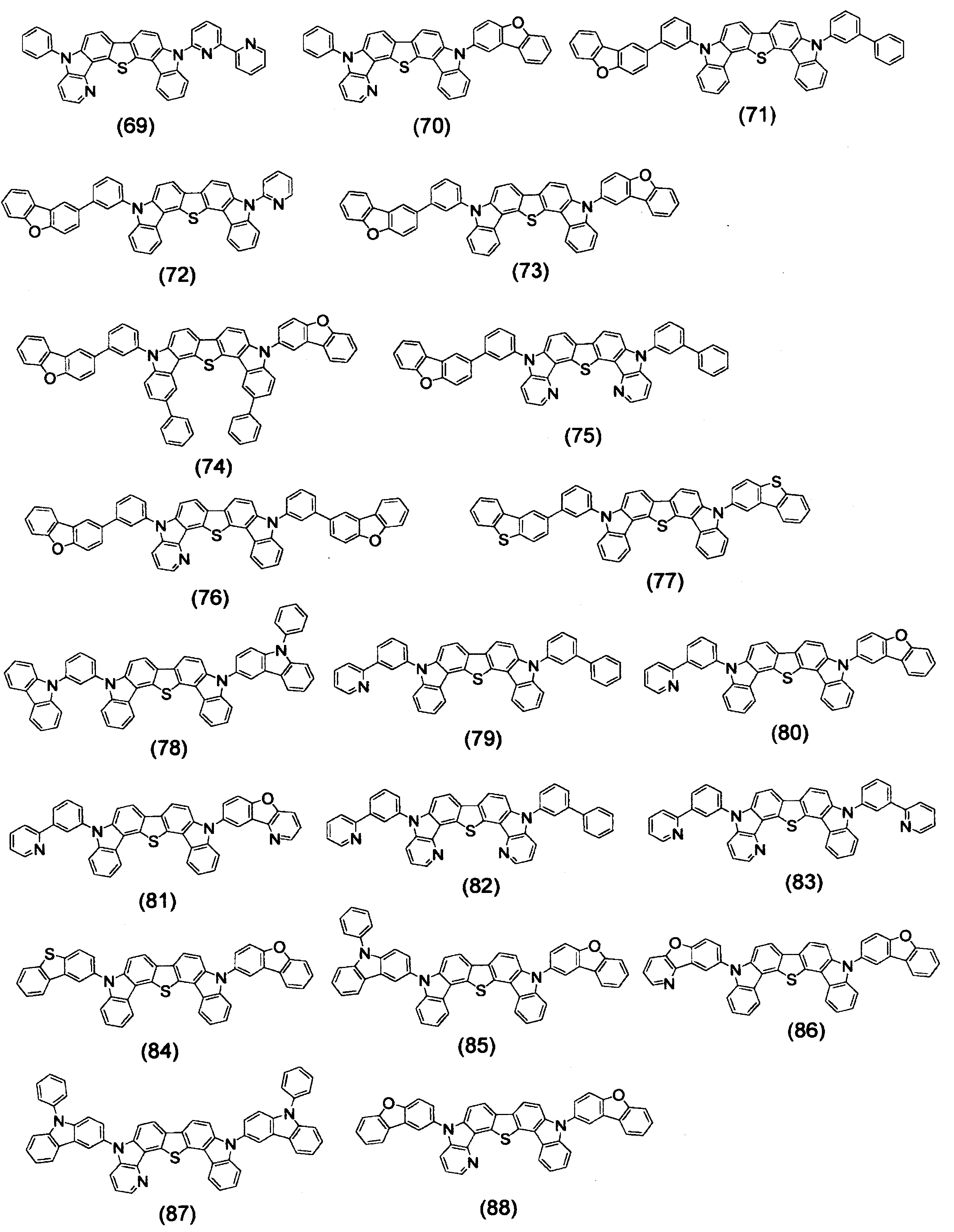


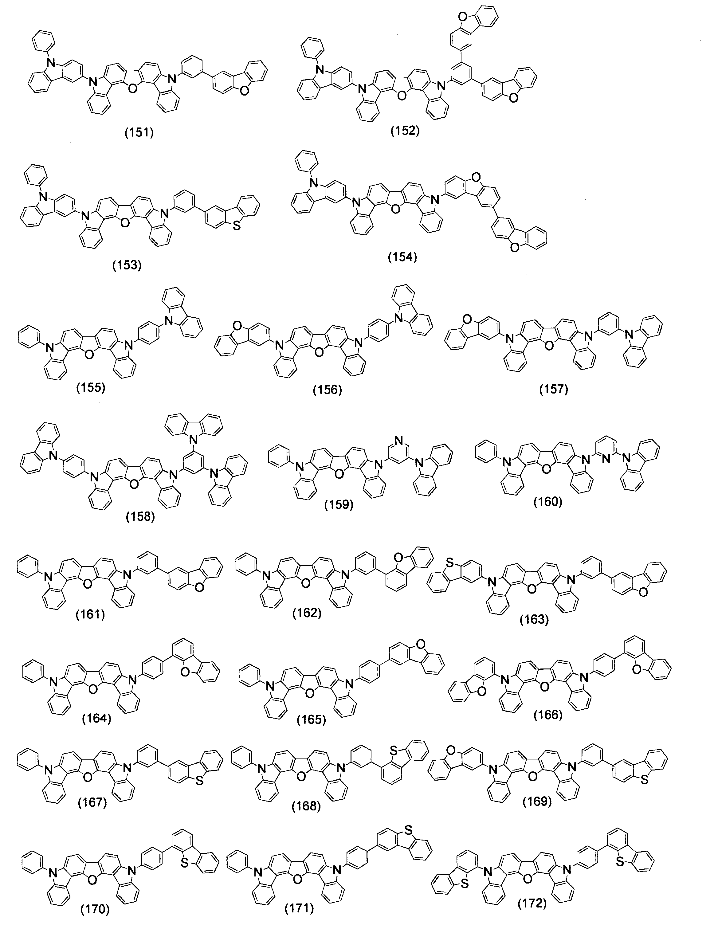

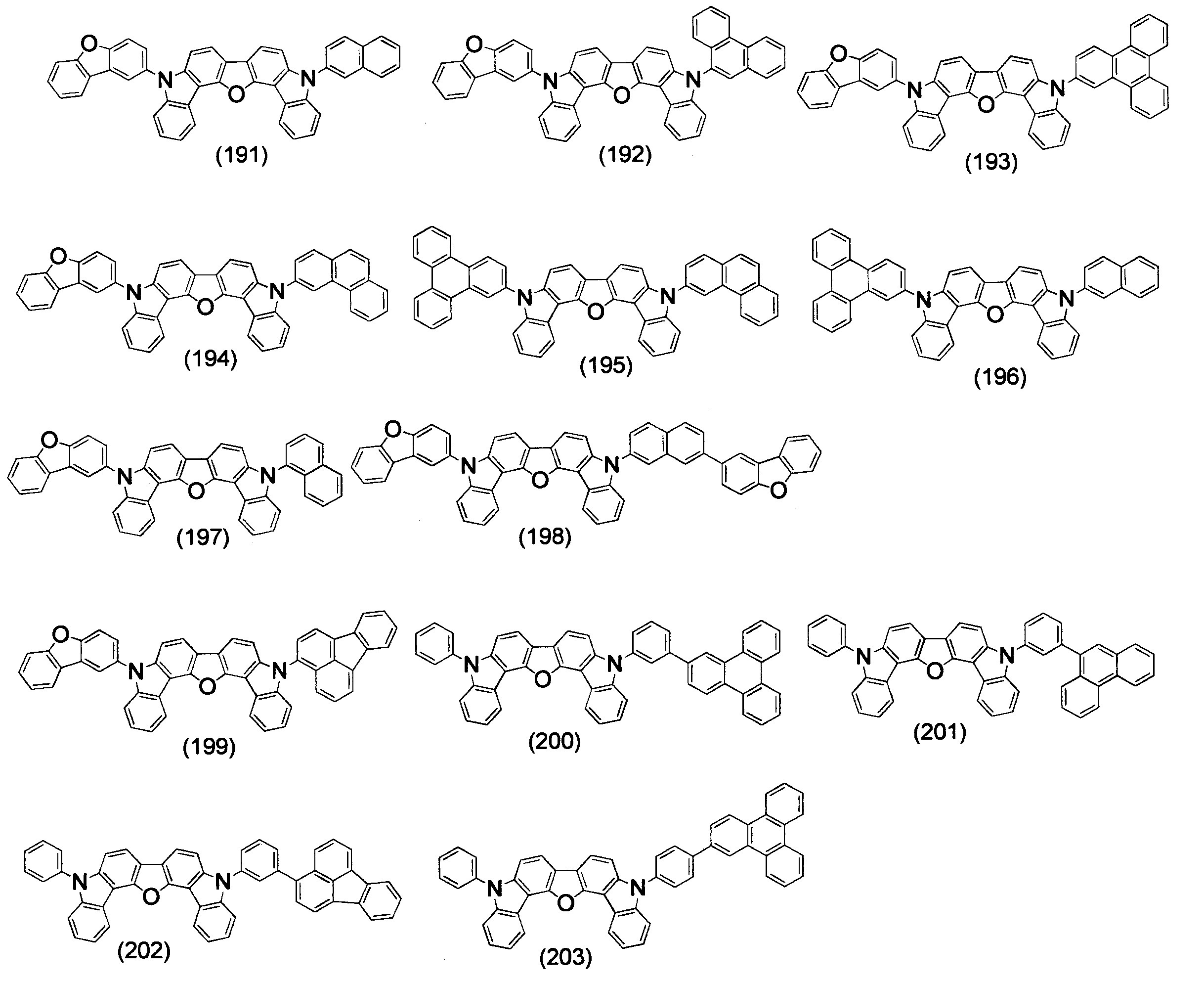

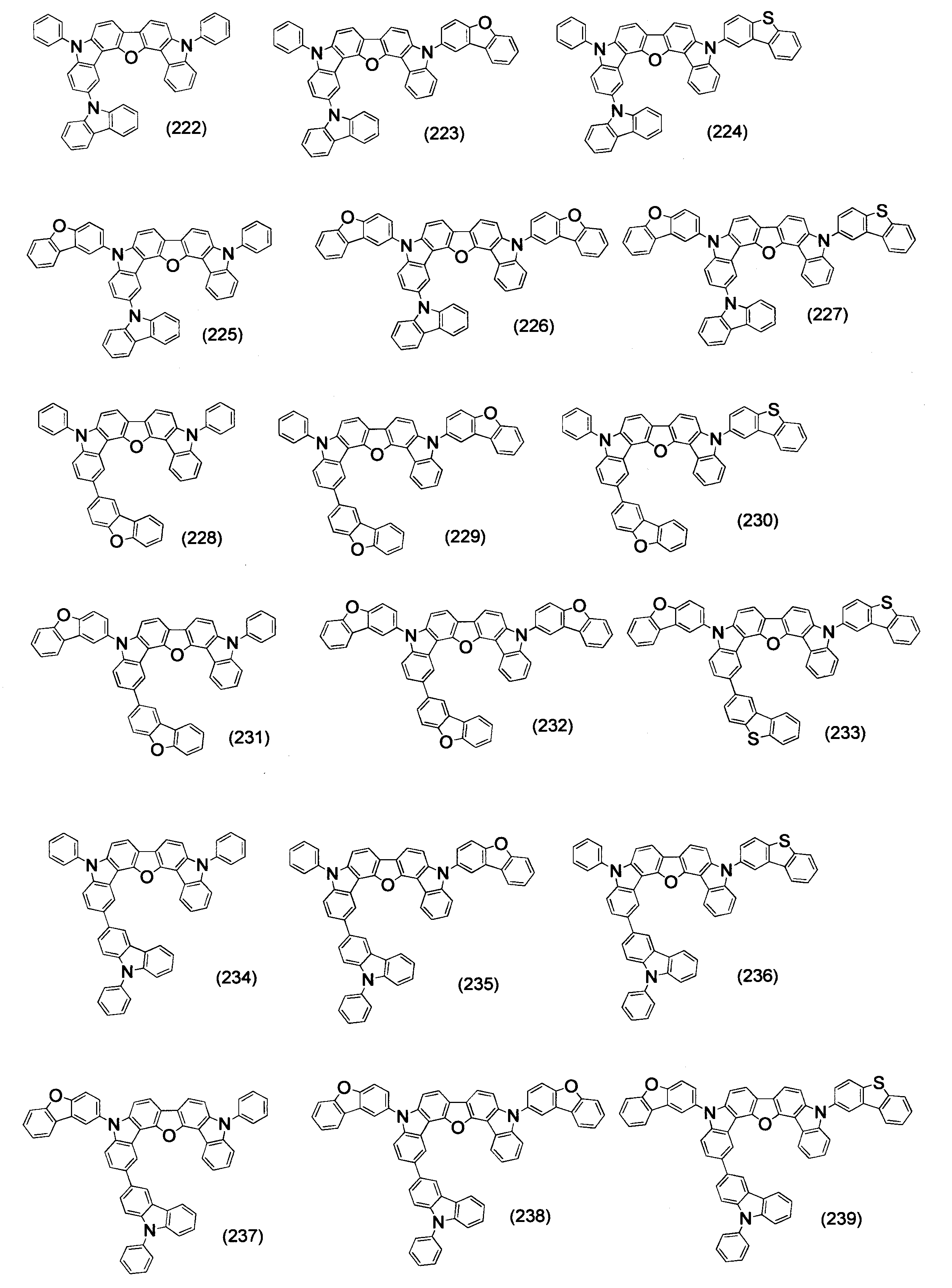
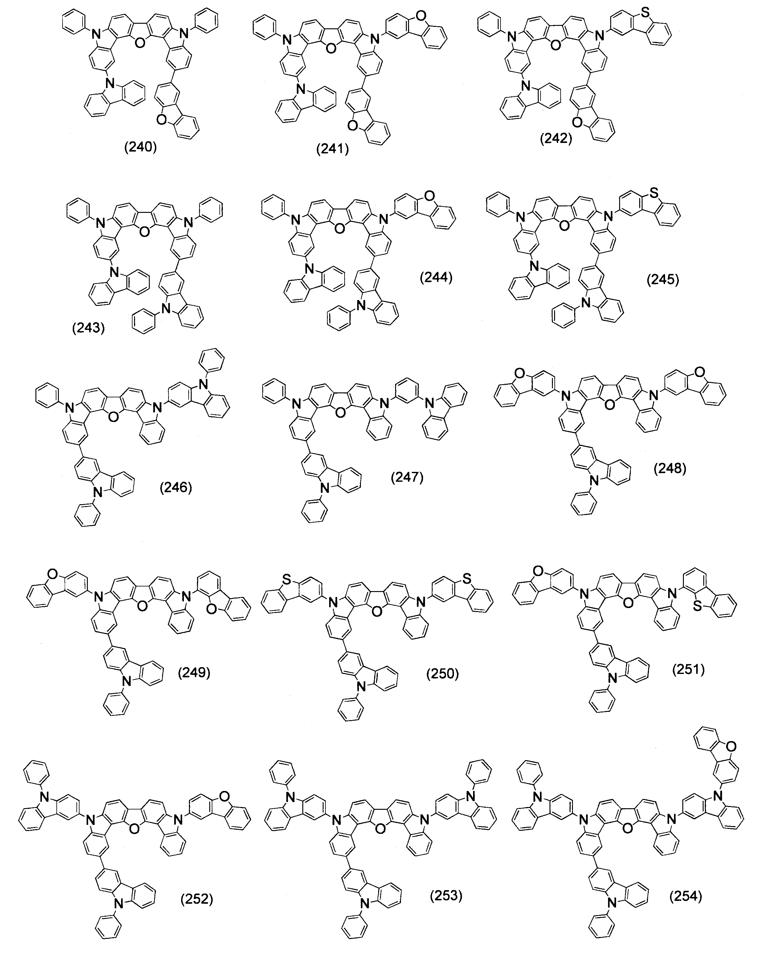
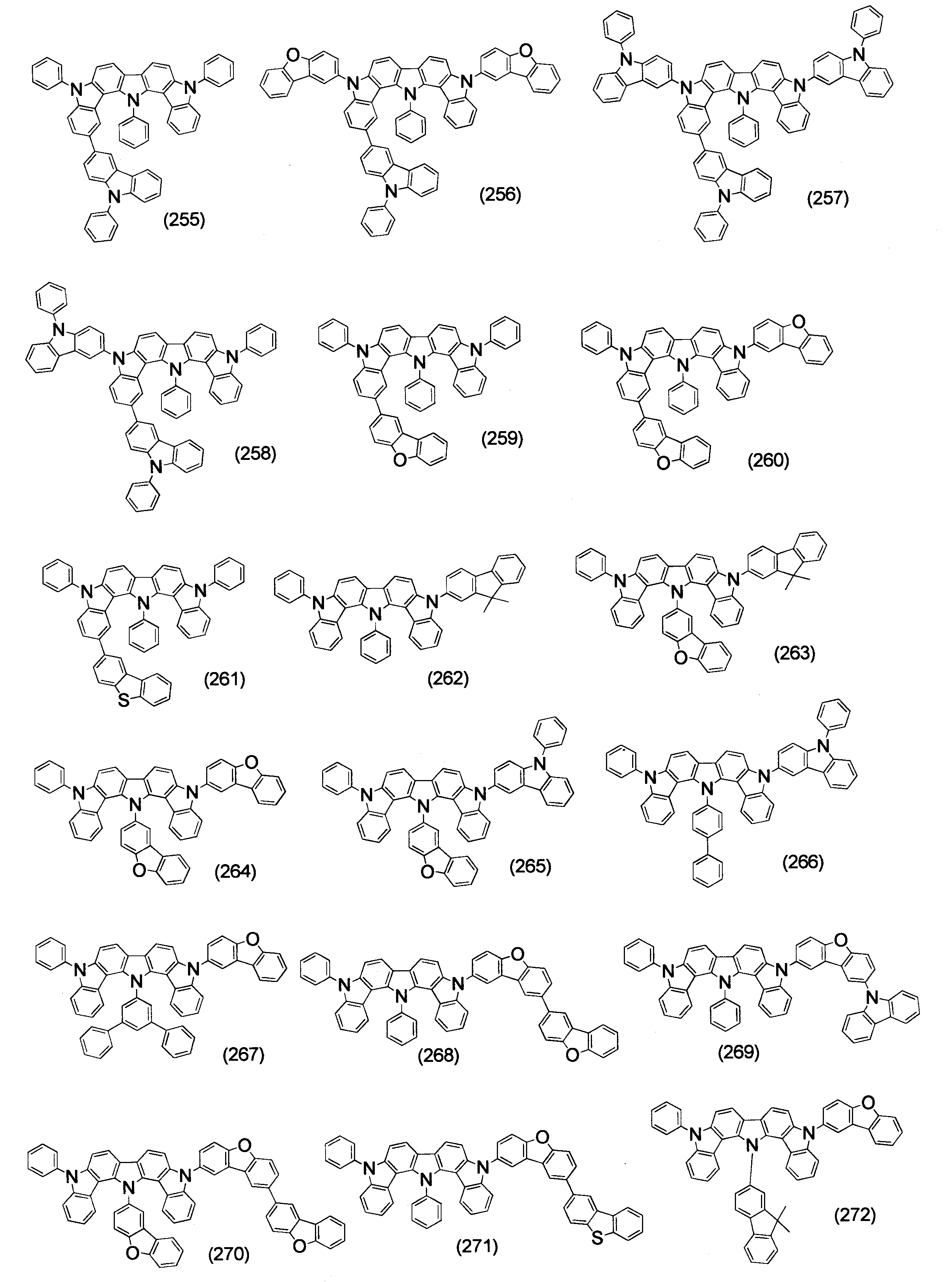
本発明の式(1)で表わされる化合物は、有機EL素子用材料として好適に使用できる。
本発明の有機EL素子用材料は、式(1)で表わされる化合物を含み、好ましくは有機EL素子用発光層材料、有機EL素子用電子障壁(阻止)層材料、又は有機EL素子用正孔障壁(阻止)層材料として用い、より好ましくは有機EL素子用発光層材料、有機EL素子用電子障壁(阻止)層材料として用いる(これらをまとめて、以下、本発明の有機EL素子用材料という場合がある)。
尚、本発明の有機EL素子用材料は、本発明の式(1)で表わされる化合物のみを含んでいてもよく、本発明の式(1)で表わされる化合物に加えて他の材料を含んでいてもよい。
本発明の有機EL素子用正孔輸送材料は、下記式(2)又は式(3)で表わされる化合物である。
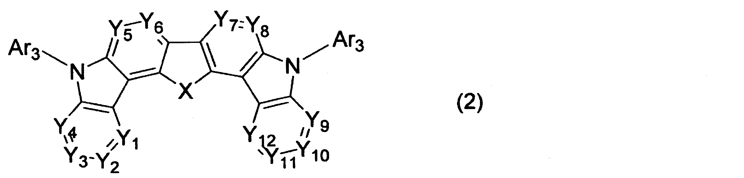
Xは、O、S、又はN-Raで表わされる基である。
Y1~Y12は、それぞれN又はC-Raで表わされる基である。
2つのAr3は、同一の置換若しくは無置換の環形成原子数5~30のヘテロアリール基である。
Raは、水素原子、重水素原子、置換基若しくは無置換の環形成炭素数6~30のアリール基、置換若しくは無置換の環形成原子数5~30のヘテロアリール基、置換若しくは無置換の炭素数1~30のアルキル基、置換若しくは無置換の炭素数1~30のフルオロアルキル基、置換若しくは無置換の環形成炭素数3~30のシクロアルキル基、置換若しくは無置換の炭素数7~30のアラルキル基、置換ホスホリル基、置換シリル基、シアノ基、ニトロ基、又はカルボキシ基である。
式(2)中に、Raが2つ以上ある場合は、複数のRaは、それぞれ同一でも異なっていてもよい。
但し、Y1とY12、Y2とY11、Y3とY10、Y4とY9、Y5とY8、及びY6とY7の全てが、それぞれ互いに同じ基である。)
式(2)の2つのAr3は、同一の置換若しくは無置換の環形成原子数5~30のヘテロアリール基であり、この置換若しくは無置換の環形成原子数5~30のヘテロアリール基は、式(1)の置換若しくは無置換の環形成原子数5~30のヘテロアリール基と同様である。
上記Ar3の環形成原子数5~30のヘテロアリール基は、好ましくは含窒素ヘテロアリール基、含酸素ヘテロアリール基、又は含硫黄ヘテロアリール基であり、より好ましくは含酸素ヘテロアリール基、又は含硫黄ヘテロアリール基である。

Xは、O、S、又はN-Raで表わされる基である。
Y1~Y12は、それぞれN又はC-Raで表わされる基である。
2つのAr4は、同一の置換若しくは無置換の環形成炭素数6~30のアリール基である。
Raは、水素原子、重水素原子、置換基若しくは無置換の環形成炭素数6~30のアリール基、置換若しくは無置換の環形成原子数5~30のヘテロアリール基、置換若しくは無置換の炭素数1~30のアルキル基、置換若しくは無置換の炭素数1~30のフルオロアルキル基、置換若しくは無置換の環形成炭素数3~30のシクロアルキル基、置換若しくは無置換の炭素数7~30のアラルキル基、置換ホスホリル基、置換シリル基、シアノ基、ニトロ基、又はカルボキシ基である。
式(3)中に、Raが2つ以上ある場合は、複数のRaは、それぞれ同一でも異なっていてもよい。
但し、Y1とY12、Y2とY11、Y3とY10、Y4とY9、Y5とY8、及びY6とY7の全てが、それぞれ互いに同じ基である。)
式(3)の2つのAr4は、同一の置換若しくは無置換の環形成炭素数6~30のアリール基であり、この置換若しくは無置換の環形成炭素数6~30のアリール基は、式(1)の置換若しくは無置換の環形成炭素数6~30のアリール基と同様である。
上記Ar4の環形成炭素数6~30のアリール基は、好ましくは、例えば、フェニル基、9,9-ジメチルフルオレニル基、9,9-ジフェニルフルオレニル基、スピロフルオレニル基、トリフェニレン環に由来する基が挙げられる。置換基を有するアリール基としては、ジベンゾフラニルフェニル基やジベンゾフルオレニルフェニル基などが挙げられる。



本発明の有機EL素子について説明する。
本発明の第1の有機EL素子は、陽極と陰極の間に、発光層を含む1層以上の有機薄膜層を有する。そして、有機薄膜層の少なくとも1層が、本発明の有機EL素子用材料を含有する。
本発明の第1の有機EL素子の一態様は、好ましくは陽極と陰極の間に、発光層を含む1層以上の有機薄膜層を有し、発光層が、本発明の有機EL素子用材料を含有する。式(1)で表わされる化合物を含む有機EL素子用材料は、発光層のホスト材料として含有するとさらに好ましい。
本発明の第1の有機EL素子の他の態様は、好ましくは陽極と陰極の間に、発光層を含む1層以上の有機薄膜層と、陽極と発光層の間にあって発光層と隣接する電子障壁(阻止)層を有し、電子障壁(阻止)層が、本発明の有機EL素子用材料を含有する。
本発明の第2の有機EL素子の他の態様は、陽極と陰極の間に、発光層を含む1層以上の有機薄膜層を有し、且つ陽極と発光層の間に正孔輸送帯域を有し、当該正孔輸送帯域が式(3)で表わされる化合物である有機エレクトロルミネッセンス素子用正孔輸送材料を含有する。
有機EL素子1は、基板10上に、陽極20、正孔輸送帯域30、燐光発光層40、電子輸送帯域50及び陰極60を、この順で積層した構成を有する。正孔輸送帯域30は、正孔輸送層、正孔注入層、電子阻止層等を意味する。同様に、電子輸送帯域50は、電子輸送層、電子注入層、正孔阻止層等を意味する。これらは形成しなくともよいが、好ましくは1層以上形成する。この素子において有機薄膜層は、正孔輸送帯域30に設けられる各有機層、燐光発光層40及び電子輸送帯域50に設けられる各有機層である。これら有機薄膜層のうち、少なくとも1層が本発明の有機EL素子用材料を含有する、又は正孔輸送帯域30のいずれか1以上の層が本発明の有機EL素子用正孔輸送材料を含有する。これにより、有機EL素子は高効率に発光できる。
尚、本発明の有機EL素子用材料を含有する有機薄膜層に対する式(1)で表わされる化合物の含有量は、好ましくは1~100重量%である。同様に、本発明の有機EL素子用正孔輸送材料を含有する正孔輸送帯域のいずれかの層に対する式(2)又は式(3)で表わされる化合物の含有量は、好ましくは1~100重量%である。
燐光量子収率が高く、発光素子の外部量子効率をより向上させることができるという点で、燐光発光性材料は、Ir,Os及びPtから選ばれる金属原子を含有する化合物であると好ましく、イリジウム錯体、オスミウム錯体、白金錯体等の金属錯体であるとさらに好ましく、中でもイリジウム錯体及び白金錯体がより好ましく、オルトメタル化イリジウム錯体が最も好ましい。燐光発光性材料は、1種単独でも、2種以上の混合物でもよい。青色の燐光発光性材料としては、例えば、後述するBD1を挙げることができる。また、ビス[2-(4’,6’-ジフルオロフェニル)ピリジナト-N,C2’]イリジウム(III)テトラキス(1-ピラゾリル)ボラート(略称:FIr6)、ビス[2-(4’,6’-ジフルオロフェニル)ピリジナト-N,C2’]イリジウム(III)ピコリナート(略称:FIrpic)、ビス[2-(3’,5’ビストリフルオロメチルフェニル)ピリジナト-N,C2’]イリジウム(III)ピコリナート(略称:Ir(CF3ppy)2(pic))、ビス[2-(4’,6’-ジフルオロフェニル)ピリジナト-N,C2’]イリジウム(III)アセチルアセトナート(略称:FIracac)などが挙げられる。
尚、障壁層(阻止層)とは、キャリアの移動障壁、又は励起子の拡散障壁の機能を有する層である。発光層から正孔輸送帯域へ電子が漏れることを防ぐための有機層を主に電子障壁層と定義し、発光層から電子輸送帯域へ正孔が漏れることを防ぐための有機層を正孔障壁層と定義することがある。また、発光層で生成された三重項励起子が、三重項エネルギーが発光層よりも低い準位を有する周辺層へ拡散することを防止するための有機層を励起子阻止層(トリプレット障壁層)と定義することがある。
また本発明の有機EL素子用材料を燐光発光層40に隣接する有機薄膜層に用い、かつさらにその隣接する有機薄膜層に接合する他の有機薄膜層に用いることもできる。
電子供与性ドーパントとしては、アルカリ金属、アルカリ金属化合物、アルカリ土類金属、アルカリ土類金属化合物、希土類金属、及び希土類金属化合物等から選ばれた少なくとも一種類が挙げられる。
有機金属錯体としては、アルカリ金属を含む有機金属錯体、アルカリ土類金属を含む有機金属錯体、及び希土類金属を含む有機金属錯体等から選ばれた少なくとも一種類が挙げられる。
アルカリ土類金属としては、カルシウム(Ca)(仕事関数:2.9eV)、ストロンチウム(Sr)(仕事関数:2.0eV以上2.5eV以下)、バリウム(Ba)(仕事関数:2.52eV)等が挙げられ、仕事関数が2.9eV以下のものが特に好ましい。
希土類金属としては、スカンジウム(Sc)、イットリウム(Y)、セリウム(Ce)、テルビウム(Tb)、イッテルビウム(Yb)等が挙げられ、仕事関数が2.9eV以下のものが特に好ましい。
以上の金属のうち好ましい金属は、特に還元能力が高く、電子注入域への比較的少量の添加により、有機EL素子における発光輝度の向上や長寿命化が可能である。
アルカリ土類金属化合物としては、酸化バリウム(BaO)、酸化ストロンチウム(SrO)、酸化カルシウム(CaO)及びこれらを混合したストロンチウム酸バリウム(BaxSr1-xO)(0<x<1)、カルシウム酸バリウム(BaxCa1-xO)(0<x<1)等が挙げられ、BaO、SrO、CaOが好ましい。
希土類金属化合物としては、フッ化イッテルビウム(YbF3)、フッ化スカンジウム(ScF3)、酸化スカンジウム(ScO3)、酸化イットリウム(Y2O3)、酸化セリウム(Ce2O3)、フッ化ガドリニウム(GdF3)、フッ化テルビウム(TbF3)等が挙げられ、YbF3、ScF3、TbF3が好ましい。
基板としてはガラス板、ポリマー板等を用いることができる。
ガラス板としては、特にソーダ石灰ガラス、バリウム・ストロンチウム含有ガラス、鉛ガラス、アルミノケイ酸ガラス、ホウケイ酸ガラス、バリウムホウケイ酸ガラス、石英等が挙げられる。また、ポリマー板としては、ポリカーボネート、アクリル、ポリエチレンテレフタレート、ポリエーテルサルフォン、ポリサルフォン等を挙げることができる。
陽極は例えば導電性材料からなり、4eVより大きな仕事関数を有する導電性材料が適している。
上記導電性材料としては、炭素、アルミニウム、バナジウム、鉄、コバルト、ニッケル、タングステン、銀、金、白金、パラジウム等及びそれらの合金、ITO基板、NESA基板に使用される酸化スズ、酸化インジウム等の酸化金属、さらにはポリチオフェンやポリピロール等の有機導電性樹脂が挙げられる。
陽極は、必要があれば2層以上の層構成により形成されていてもよい。発光層からの発光を陽極から取り出す場合、陰極の発光に対する透過率は10%より大きくすることが好ましい。
陰極は例えば導電性材料からなり、4eVより小さな仕事関数を有する導電性材料が適している。
上記導電性材料としては、マグネシウム、カルシウム、錫、鉛、チタニウム、イットリウム、リチウム、ルテニウム、マンガン、アルミニウム、フッ化リチウム等及びこれらの合金が挙げられるが、これらに限定されるものではない。
また、上記合金としては、マグネシウム/銀、マグネシウム/インジウム、リチウム/アルミニウム等が代表例として挙げられるが、これらに限定されるものではない。合金の比率は、蒸着源の温度、雰囲気、真空度等により制御され、適切な比率に選択される。
陰極は、必要があれば2層以上の層構成により形成されていてもよく、陰極は上記導電性材料を蒸着やスパッタリング等の方法により薄膜を形成させることにより、作製することができる。
また、陰極としてのシート抵抗は数百Ω/□以下が好ましく、膜厚は通常10nm~1μmであり、好ましくは50~200nmである。
本発明の有機EL素子用材料以外の材料で燐光発光層を形成する場合、燐光発光層の材料として公知の材料が使用できる。具体的には、特願2005-517938等を参照すればよい。
本発明の第1の有機EL素子は、図2に示す素子のように蛍光発光層70を有していてもよい。蛍光発光層としては、本発明の有機EL素子用材料の他、公知の材料が使用できる。
また、2種類の発光材料(ドーパント材料)を用いるダブルドーパントとしてもよい。発光層において、量子収率の高いドーパント材料を2種類以上入れることによって、それぞれのドーパントが発光する。例えば、ホストと赤色ドーパント、緑色のドーパントを共蒸着することによって、黄色の発光層を実現することがある。
発光層は単層でもよく、また、積層構造でもよい。発光層を積層させると、発光層界面に電子と正孔を蓄積させることによって再結合領域を発光層界面に集中させることができる場合がある。このような場合、量子効率を向上させる。
正孔注入・輸送層は、発光層への正孔注入を助け、発光領域まで輸送する層であって、正孔移動度が大きく、イオン化エネルギーが小さい層である。正孔注入・輸送層は、単層構造でもよく、正孔注入層と正孔輸送層が積層された多層構造でもよい。更に、正孔注入層が多層構造であってもよく、正孔輸送層が多層構造であってもよい。この場合、発光層と接する層を、電子障壁(阻止)層としてもよい。電子障壁(阻止)用材料として、本発明の有機EL素子用材料を含有する材料を用いることができる。
正孔注入・輸送層の材料としては、より低い電界強度で正孔を発光層に輸送する材料が好ましく、さらに正孔の移動度が、例えば104~106V/cmの電界印加時に、少なくとも10-4cm2/V・秒であれば好ましい。
また、p型Si、p型SiC等の無機化合物も正孔注入材料として使用することができる。
電子注入・輸送層は、発光層への電子の注入を助け、発光領域まで輸送する層であって、電子移動度が大きい層である。電子注入・輸送層は、単層構造でもよく、電子注入層と電子輸送層が積層された多層構造でもよい。更に、電子注入層が多層構造であってもよく、電子輸送層が多層構造であってもよい。この場合、発光層と接する層を、正孔障壁(阻止)層としてもよい。正孔障壁(阻止)用材料としては、公知の材料を用いることができる。例えば、後述する実施例2で用いた化合物(H1)が挙げられる。
有機EL素子は発光した光が電極(例えば陰極)により反射するため、直接陽極から取り出される発光と、電極による反射を経由して取り出される発光とが干渉することが知られている。この干渉効果を効率的に利用するため、電子注入・輸送層は数nm~数μmの膜厚で適宜選ばれるが、特に膜厚が厚いとき、電圧上昇を避けるために、104~106V/cmの電界印加時に電子移動度が少なくとも10-5cm2/Vs以上であることが好ましい。
各層の膜厚は特に限定されるものではないが、適切な膜厚に設定する必要がある。膜厚が厚すぎると、一定の光出力を得るために大きな印加電圧が必要になり効率が悪くなる。膜厚が薄すぎるとピンホール等が発生して、電界を印加しても充分な発光輝度が得られない。通常の膜厚は5nm~10μmの範囲が適しているが、10nm~0.2μmの範囲がさらに好ましい。
本発明の第2の有機EL素子では、上述した本発明の有機EL素子用正孔輸送材料を使用した層以外の構成については、特に限定されず、公知の材料等を使用できる。以下、第2の有機EL素子の各層について簡単に説明するが、本発明の第2の有機EL素子に適用される材料は以下に限定されない。
有機EL素子を構成する、基板、陽極、陰極、電子注入層及び電子輸送層は、上述した第1の有機EL素子と同様である。
発光層も上述した第1の有機EL素子と同様であるが、本発明の有機EL素子用材料を必ずしも用いなくてもよい。好適には、発光層に本発明の有機EL素子用材料を用いる。
正孔注入層及び正孔輸送層も、上述した第1の有機EL素子と同様であるが、本発明の有機EL素子用正孔輸送材料を正孔輸送層、正孔注入層又は電子阻止層のいずれか1層以上に用いる必要がある。
実施例1(化合物(7)の合成)
(1)化合物(7-a)の合成
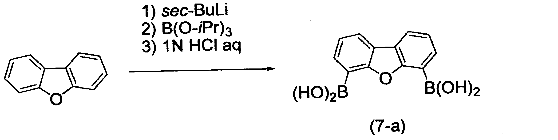
収量は15.9g、収率は93%であった。
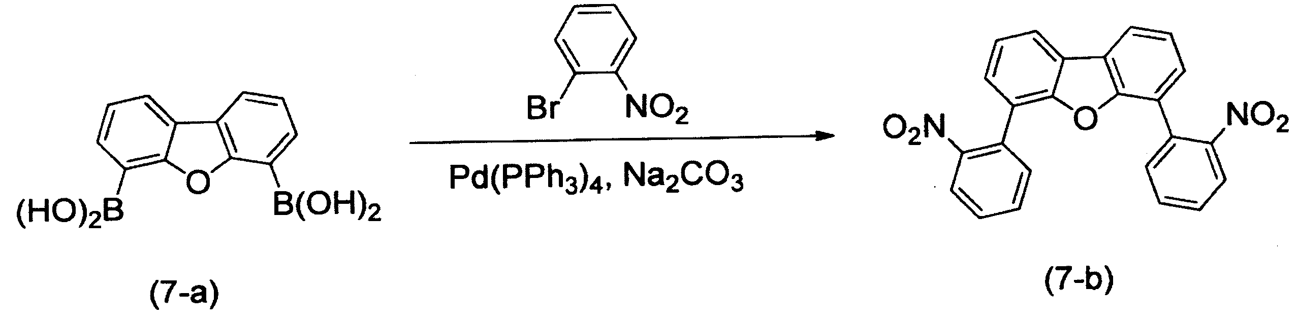
反応終了後、試料溶液をろ過し、得られた固体をメタノール,ヘキサンにて洗浄して、化合物(7-b)を得た。
収量は26.5g、収率は66%であった。

反応終了後、蒸留を行い、残った亜リン酸トリエチル、亜リン酸トリエチル残差を除去し、得られた有機層をシリカゲルクロマトグラフィー(ヘキサン:ジクロロメタン=10:1~5:1~1:1)で精製し、黄色の固体である化合物(7-c)を得た。
収量は2.22g、収率は54%であった。
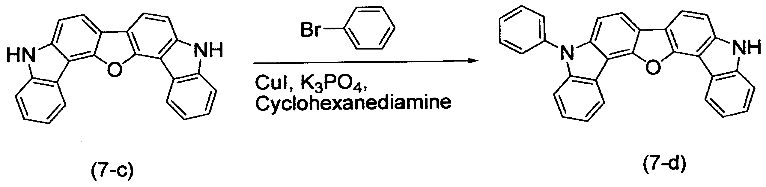
反応終了後、反応物をセライトろ過し、これを分液ロートに移し、ジクロロメタンにて数回抽出した。得られた有機層を無水硫酸マグネシウムで乾燥、ろ過、濃縮した。これをシリカゲルクロマトグラフィー(ヘキサン:ジクロロメタン=10:1~5:1)で精製し、白色の固体である化合物(7-d)を得た。
収量は0.644g、収率は53%であった。
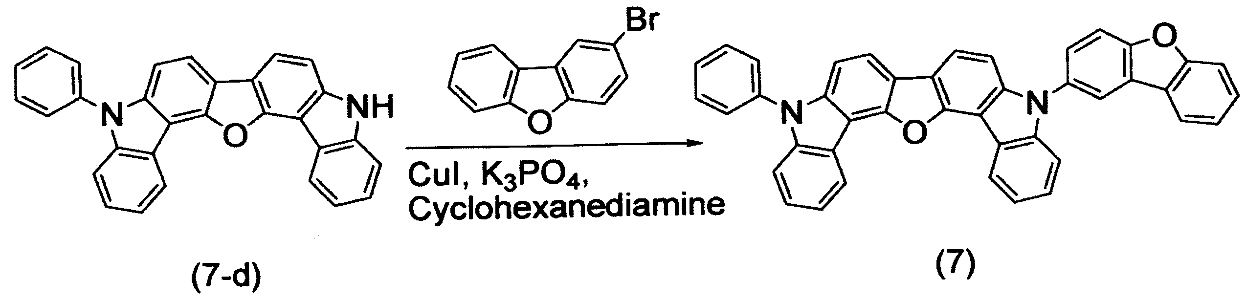
反応終了後、反応物をセライトろ過し、これを分液ロートに移し、ジクロロメタンにて数回抽出した。得られた有機層を無水硫酸マグネシウムで乾燥、ろ過、濃縮した。これをシリカゲルクロマトグラフィー(ヘキサン:ジクロロメタン=10:1~5:1)で精製し、白色の固体である化合物(7)を得た。
収量は0.644g、収率は78%であった。
同定はFD/MSによる分子量測定によって行い、分子量588に対してm/e=588であった。
実施例2
膜厚130nmのITO電極ライン付きガラス基板(ジオマティック社製)を、イソプロピルアルコール中で5分間、超音波洗浄した後、UVオゾン洗浄を30分間行なった。
洗浄後のITO電極ライン付きガラス基板を真空蒸着装置の基板ホルダーに装着し、まずITO電極ラインが形成されている側の面上に、ITO電極ラインを覆うようにして化合物(HI1)を厚さ20nmで、次いで化合物(HT1)を厚さ60nmで抵抗加熱蒸着し、順次薄膜を成膜した。成膜レートは1Å/sとした。これらの薄膜は、それぞれ正孔注入層及び正孔輸送層として機能する。
次に、正孔注入・輸送層上に、化合物(7)と化合物(BD1)を同時に抵抗加熱蒸着して膜厚50nmの薄膜を成膜した。このとき、化合物(BD1)を、化合物(7)と化合物(BD1)の総質量に対し質量比で20%になるように蒸着した。成膜レートはそれぞれ1.2Å/s、0.3Å/sとした。この薄膜は、燐光発光層として機能する。
次に、この燐光発光層上に、化合物(H1)を抵抗加熱蒸着して膜厚10nmの薄膜を成膜した。成膜レートは1.2Å/sとした。この薄膜は障壁層として機能する。
次に、この障壁層上に、化合物(ET1)を抵抗加熱蒸着して膜厚10nmの薄膜を成膜した。成膜レートは1Å/sとした。この膜は電子注入層として機能する。
次に、この電子注入層上に膜厚1.0nmのLiFを成膜レート0.1Å/sで蒸着した。
次に、このLiF膜上に金属アルミニウムを成膜レート8.0Å/sにて蒸着し、膜厚80nmの金属陰極を形成して有機EL素子を製造した。

(1)外部量子効率(%)
23℃、乾燥窒素ガス雰囲気下で、輝度1000cd/m2時の外部量子効率を輝度計(ミノルタ社製分光輝度放射計CS-1000)を用いて測定した。
燐光ホスト材料として化合物(7)の代わりに化合物(H2)を用いた以外は、実施例1と同様にして有機EL素子を作製し、評価した。結果を表1に示す。
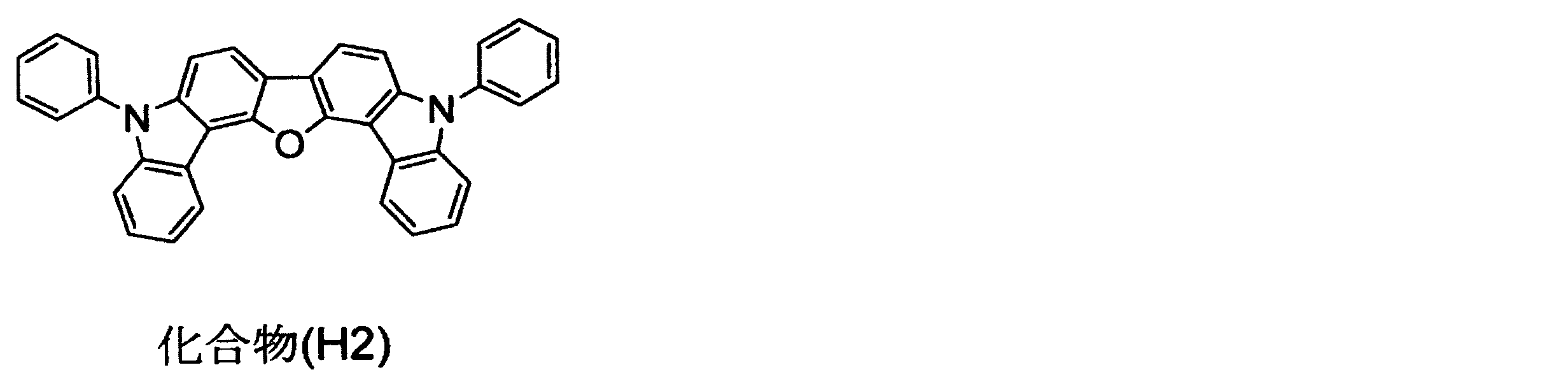

実施例3(化合物(40)の合成)
(1)化合物(40-a)の合成

反応終了後、反応物をセライトろ過し、これを分液ロートに移し、トルエンにて数回抽出した。得られた有機層を無水硫酸マグネシウムで乾燥、ろ過、濃縮した。これをシリカゲルクロマトグラフィー(ヘキサン:トルエン=10:1~5:1~2:1)で精製し、白色の固体である化合物(40-a)を得た。
収量は11.8g、収率は23%であった。

反応終了後、溶媒を減圧下で留去し、残渣にトルエン2000mLを加えて、100℃に加熱した。不溶物をシリカゲルで濾去し、濾液を濃縮することにより得られた固体をアセトンによる懸濁洗浄で精製し、白色の固体である化合物(40)を得た。
収量は3.1g、収率は45%であった。
同定はFD/MSによる分子量測定によって行い、分子量694に対してm/e=694であった。
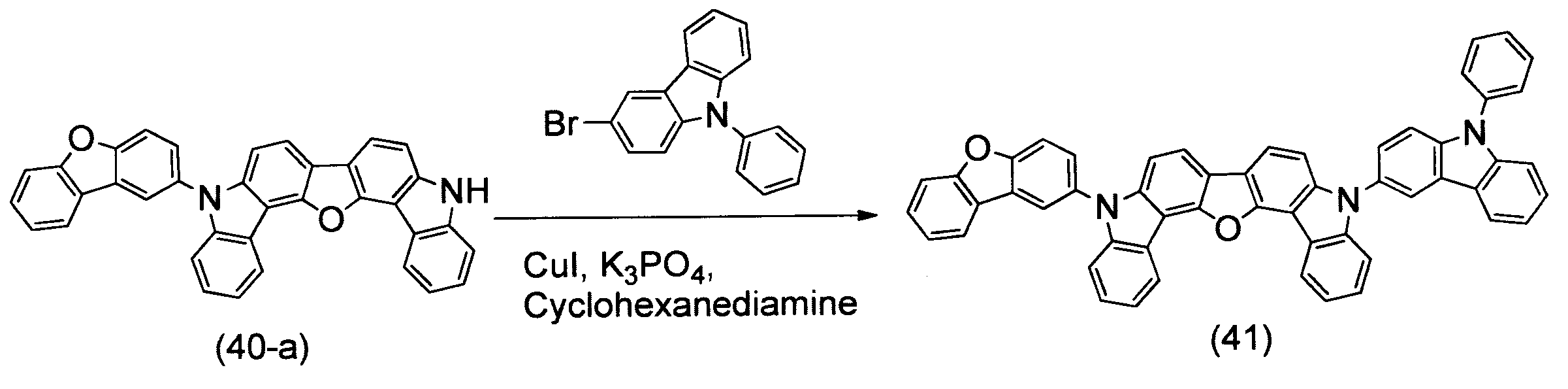
反応終了後、反応物をセライトろ過し、これを分液ロートに移し、ジクロロメタンにて数回抽出した。得られた有機層を無水硫酸マグネシウムで乾燥、ろ過、濃縮した。これをシリカゲルクロマトグラフィー(ヘキサン:ジクロロメタン=4:1~2:1)で精製し、白色の固体である化合物(41)を得た。
収量は2.9g、収率は38%であった。
同定はFD/MSによる分子量測定によって行い、分子量753に対してm/e=753であった。

反応終了後、反応物をセライトろ過し、これを分液ロートに移し、トルエン及びジクロロメタンにて数回抽出した。得られた有機層を合わせて無水硫酸マグネシウムで乾燥、ろ過、濃縮した。これをシリカゲルクロマトグラフィー(ヘキサン:ジクロロメタン=2:1~1:2~1:10)で精製し、白色の固体である化合物(42)を得た。
収量は1.4g、収率は21%であった。
同定はFD/MSによる分子量測定によって行い、分子量679に対してm/e=679であった。

(1)化合物(128-a)の合成

反応終了後、有機相を分取し、無水硫酸マグネシウムで乾燥後、溶媒を減圧下で留去した。残渣をシリカゲルカラムクロマトグラフィー(ヘキサン:トルエン=2:1~1:2)で精製し、白色の固体である化合物(128-a)を得た。
収量は15.3g、収率は55%であった。

反応終了後、溶媒を減圧下で留去して得られた残渣をトルエンで希釈し、析出物を濾別してから、シリカゲルカラムクロマトグラフィー(ヘキサン:トルエン=1:1~1:3)で精製し、白色の固体である化合物(128-b)を得た。
収量は6.1g、収率は45%であった。

反応終了後、溶媒を減圧下で留去して得られた残渣をシリカゲルカラムクロマトグラフィー(ヘキサン:トルエン=1:1~1:3)で精製し、白色の固体である化合物(128-c)を得た。
収量は1.4g、収率は33%であった。

反応終了後、溶媒を減圧下で留去して得られた残渣をシリカゲルカラムクロマトグラフィー(ヘキサン:トルエン=1:1~1:3)で精製し、白色の固体である化合物(128-c)を得た。
収量は0.9g、収率は64%であった。
出発原料として化合物(7-c)の代わりに、化合物(128-d)を用いることにより、実施例3に記載した方法に従い、化合物(128)を合成した。

実施例8
化合物(H1)の代わりに、化合物(H3)を用いた以外は、実施例2と同様にして有機EL素子を作製した。
作製した有機EL素子は直流電流駆動により発光させ、輝度、電流密度を測定し、電流密度1mA/cm2における電圧及び発光効率(外部量子効率)を求めた。さらに初期輝度3,000cd/m2における輝度70%寿命(輝度が70%まで低下する時間)を比較例の素子を100とした場合の相対値で記載した。これら発光性能の評価結果を表2に示す。
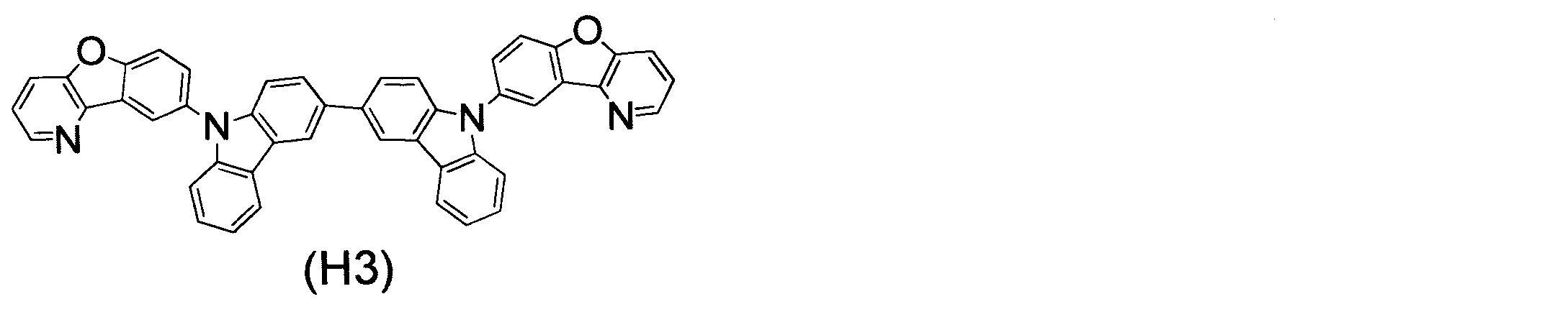
燐光ホスト材料として化合物(7)の代わりに、それぞれ表2に記載した化合物を用いた以外は、実施例8と同様にして有機EL素子を作製し、評価した。結果を表2に示す。
燐光ホスト材料として化合物(7)の代わりに化合物(H2)を用いた以外は、実施例8と同様にして有機EL素子を作製し、評価した。結果を表2に示す。
燐光ホスト材料として化合物(7)の代わりに化合物(H4)を用いた以外は、実施例8と同様にして有機EL素子を作製し、評価した。結果を表2に示す。
燐光ホスト材料として化合物(7)の代わりに化合物(H5)を用いた以外は、実施例8と同様にして有機EL素子を作製し、評価した。結果を表2に示す。
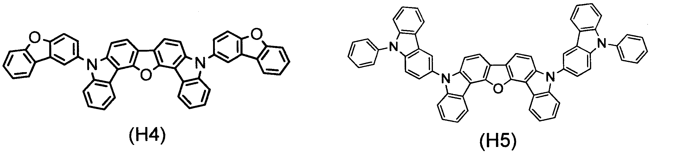

本発明の有機EL素子は、壁掛けテレビのフラットパネルディスプレイ等の平面発光体、複写機、プリンター、液晶ディスプレイのバックライト又は計器類等の光源、表示板、標識灯等に利用できる。
本願のパリ優先の基礎となる日本出願明細書の内容を全てここに援用する。
Claims (18)
- 下記式(1)で表わされる化合物。
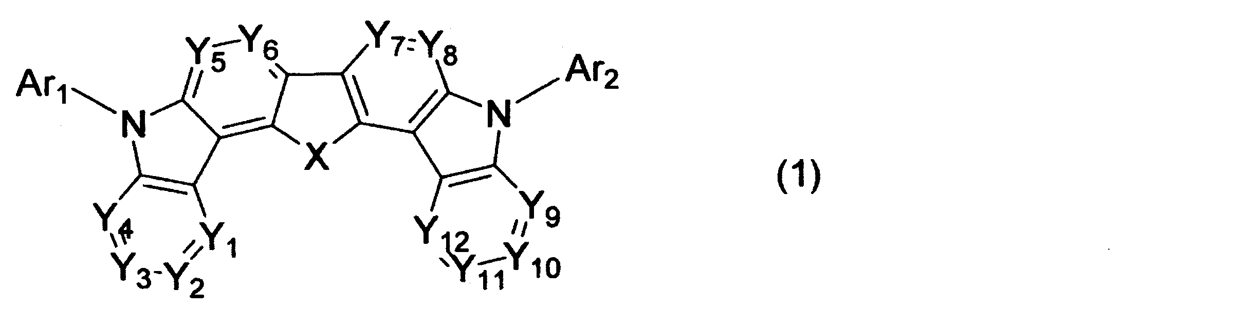
Xは、O、S、又はN-Raで表わされる基である。
Y1~Y12は、それぞれN又はC-Raで表わされる基である。
Ar1及びAr2は、それぞれ置換若しくは無置換の環形成炭素数6~30のアリール基、又は、置換若しくは無置換の環形成原子数5~30のヘテロアリール基である。
Raは、水素原子、重水素原子、置換基若しくは無置換の環形成炭素数6~30のアリール基、置換若しくは無置換の環形成原子数5~30のヘテロアリール基、置換若しくは無置換の炭素数1~30のアルキル基、置換若しくは無置換の炭素数1~30のフルオロアルキル基、置換若しくは無置換の環形成炭素数3~30のシクロアルキル基、置換若しくは無置換の炭素数7~30のアラルキル基、置換ホスホリル基、置換シリル基、置換ゲルマニウム基、シアノ基、ニトロ基、又はカルボキシ基である。
式(1)中に、Raが2つ以上ある場合は、複数のRaは、それぞれ同一でも異なっていてもよい。
但し、Ar1とAr2が同一の置換基である場合、Y1とY12、Y2とY11、Y3とY10、Y4とY9、Y5とY8、及びY6とY7の全てが、それぞれ互いに同じ基とはならない。) - 前記式(1)のAr1及びAr2が、それぞれ置換若しくは無置換の環形成炭素数6~30のアリール基である請求項1に記載の化合物。
- 前記式(1)のAr1及びAr2が、それぞれ置換若しくは無置換の環形成原子数53~30のヘテロアリール基である請求項1に記載の化合物。
- 前記式(1)のXが、N-Raで表わされる基である請求項1~3のいずれかに記載の化合物。
- 前記式(1)のXが、O又はSである請求項1~3のいずれかに記載の化合物。
- 前記式(1)のY1~Y12が、それぞれC-Raで表わされる基である請求項1~5のいずれかに記載の化合物。
- 前記式(1)のAr1が、-L1-R1で表される請求項1~6のいずれかに記載の化合物。
(L1は、置換若しくは無置換の環形成炭素数6~30のアリーレン基、又は、置換若しくは無置換の環形成原子数5~30のヘテロアリーレン基を表し、R1は、置換若しくは無置換の環形成炭素数6~30のアリール基、又は、置換若しくは無置換の環形成原子数5~30のヘテロアリール基を表す。) - L1が、置換若しくは無置換の環形成炭素数6~30のアリーレン基を表す請求項7に記載の化合物。
- L1が、置換若しくは無置換の環形成原子数5~30のヘテロアリーレン基を表す請求項7に記載の化合物。
- 請求項1~9のいずれかに記載の化合物を含む有機エレクトロルミネッセンス素子用材料。
- 下記式(2)で表わされる有機エレクトロルミネッセンス素子用正孔輸送材料。
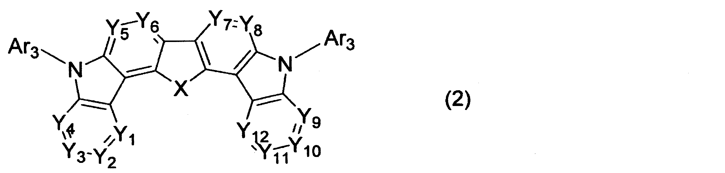
Xは、O、S、又はN-Raで表わされる基である。
Y1~Y12は、それぞれN又はC-Raで表わされる基である。
2つのAr3は、同一の置換若しくは無置換の環形成原子数5~30のヘテロアリール基である。
Raは、水素原子、重水素原子、置換基若しくは無置換の環形成炭素数6~30のアリール基、置換若しくは無置換の環形成原子数5~30のヘテロアリール基、置換若しくは無置換の炭素数1~30のアルキル基、置換若しくは無置換の炭素数1~30のフルオロアルキル基、置換若しくは無置換の環形成炭素数3~30のシクロアルキル基、置換若しくは無置換の炭素数7~30のアラルキル基、置換ホスホリル基、置換シリル基、シアノ基、ニトロ基、又はカルボキシ基である。
式(2)中に、Raが2つ以上ある場合は、複数のRaは、それぞれ同一でも異なっていてもよい。
但し、Y1とY12、Y2とY11、Y3とY10、Y4とY9、Y5とY8、及びY6とY7の全てが、それぞれ互いに同じ基である。) - 下記式(3)で表わされる有機エレクトロルミネッセンス素子用正孔輸送材料。

Xは、O、S、又はN-Raで表わされる基である。
Y1~Y12は、それぞれN又はC-Raで表わされる基である。
2つのAr4は、同一の置換若しくは無置換の環形成炭素数6~30のアリール基である。
Raは、水素原子、重水素原子、置換基若しくは無置換の環形成炭素数6~30のアリール基、置換若しくは無置換の環形成原子数5~30のヘテロアリール基、置換若しくは無置換の炭素数1~30のアルキル基、置換若しくは無置換の炭素数1~30のフルオロアルキル基、置換若しくは無置換の環形成炭素数3~30のシクロアルキル基、置換若しくは無置換の炭素数7~30のアラルキル基、置換ホスホリル基、置換シリル基、シアノ基、ニトロ基、又はカルボキシ基である。
式(3)中に、Raが2つ以上ある場合は、複数のRaは、それぞれ同一でも異なっていてもよい。
但し、Y1とY12、Y2とY11、Y3とY10、Y4とY9、Y5とY8、及びY6とY7の全てが、それぞれ互いに同じ基である。) - 陽極と陰極の間に、発光層を含む1層以上の有機薄膜層を有し、前記有機薄膜層の少なくとも1層が請求項10に記載の有機エレクトロルミネッセンス素子用材料を含有する有機エレクトロルミネッセンス素子。
- 前記発光層が前記有機エレクトロルミネッセンス素子用材料を含む請求項13に記載の有機エレクトロルミネッセンス素子。
- 前記陰極と前記発光層の間に電子輸送帯域を有し、該電子輸送帯域が前記有機エレクトロルミネッセンス素子用材料を含む請求項14に記載の有機エレクトロルミネッセンス素子。
- 陽極と陰極の間に、発光層を含む1層以上の有機薄膜層を有し、
前記陽極と前記発光層の間に正孔輸送帯域を有し、該正孔輸送帯域が請求項11に記載の有機エレクトロルミネッセンス素子用正孔輸送材料を含有する有機エレクトロルミネッセンス素子。 - 陽極と陰極の間に、発光層を含む1層以上の有機薄膜層を有し、
前記陽極と前記発光層の間に正孔輸送帯域を有し、該正孔輸送帯域が請求項12に記載の有機エレクトロルミネッセンス素子用正孔輸送材料を含有する有機エレクトロルミネッセンス素子。 - 前記発光層が燐光発光材料を含有し、前記燐光発光材料がイリジウム(Ir)、オスミウム(Os)及び白金(Pt)から選択される金属原子のオルトメタル化錯体である請求項13~17のいずれかに記載の有機エレクトロルミネッセンス素子。
Priority Applications (4)
| Application Number | Priority Date | Filing Date | Title |
|---|---|---|---|
| JP2014540752A JP6220341B2 (ja) | 2012-10-11 | 2013-10-10 | ラダー化合物、及びそれを用いた有機エレクトロルミネッセンス素子 |
| KR1020157009039A KR102232990B1 (ko) | 2012-10-11 | 2013-10-10 | 래더 화합물 및 그것을 사용한 유기 전계 발광 소자 |
| CN201380053087.2A CN104718210B (zh) | 2012-10-11 | 2013-10-10 | 梯形化合物以及使用其的有机电致发光元件 |
| US14/435,126 US9960364B2 (en) | 2012-10-11 | 2013-10-10 | Ladder compound, and organic electroluminescent element using same |
Applications Claiming Priority (2)
| Application Number | Priority Date | Filing Date | Title |
|---|---|---|---|
| JP2012-225916 | 2012-10-11 | ||
| JP2012225916 | 2012-10-11 |
Publications (1)
| Publication Number | Publication Date |
|---|---|
| WO2014057684A1 true WO2014057684A1 (ja) | 2014-04-17 |
Family
ID=50477166
Family Applications (1)
| Application Number | Title | Priority Date | Filing Date |
|---|---|---|---|
| PCT/JP2013/006061 Ceased WO2014057684A1 (ja) | 2012-10-11 | 2013-10-10 | ラダー化合物、及びそれを用いた有機エレクトロルミネッセンス素子 |
Country Status (5)
| Country | Link |
|---|---|
| US (1) | US9960364B2 (ja) |
| JP (1) | JP6220341B2 (ja) |
| KR (1) | KR102232990B1 (ja) |
| CN (1) | CN104718210B (ja) |
| WO (1) | WO2014057684A1 (ja) |
Cited By (10)
| Publication number | Priority date | Publication date | Assignee | Title |
|---|---|---|---|---|
| WO2014148047A1 (ja) * | 2013-03-22 | 2014-09-25 | 出光興産株式会社 | ヘテロ縮合環を有するアミン化合物及びそれを用いた有機エレクトロルミネッセンス素子 |
| WO2015159706A1 (ja) * | 2014-04-16 | 2015-10-22 | 出光興産株式会社 | 化合物、有機エレクトロルミネッセンス素子および電子機器 |
| WO2015198988A1 (ja) * | 2014-06-26 | 2015-12-30 | 出光興産株式会社 | 有機エレクトロルミネッセンス素子、有機エレクトロルミネッセンス素子用材料、および電子機器 |
| WO2015198987A1 (ja) * | 2014-06-26 | 2015-12-30 | 出光興産株式会社 | 有機エレクトロルミネッセンス素子、有機エレクトロルミネッセンス素子用材料、および電子機器 |
| WO2017038728A1 (ja) * | 2015-08-28 | 2017-03-09 | 出光興産株式会社 | 化合物、有機エレクトロルミネッセンス素子用材料、有機エレクトロルミネッセンス素子、及び電子機器 |
| WO2017118155A1 (zh) * | 2016-01-07 | 2017-07-13 | 广州华睿光电材料有限公司 | 一种有机光电材料及其用途 |
| CN110494436A (zh) * | 2017-05-12 | 2019-11-22 | 株式会社Lg化学 | 杂环化合物及包含其的有机发光元件 |
| KR20200122854A (ko) * | 2019-04-19 | 2020-10-28 | (주)알로스 | 신규한 유기 발광 화합물 및 이를 포함하는 유기 발광 소자 |
| US11124521B2 (en) | 2018-04-11 | 2021-09-21 | Samsung Electronics Co., Ltd. | Condensed cyclic compound and organic light-emitting device including the same |
| US12144249B2 (en) | 2020-07-17 | 2024-11-12 | Samsung Sdi Co., Ltd. | Compound for organic optoelectronic device, composition for organic optoelectronic device, organic optoelectronic device and display device |
Families Citing this family (2)
| Publication number | Priority date | Publication date | Assignee | Title |
|---|---|---|---|---|
| EP3333918B1 (en) * | 2015-08-04 | 2020-03-04 | FUJIFILM Corporation | Organic thin-film transistor and method for producing same, organic thin-film transistor material, organic thin-film transistor composition, compound, and organic semiconductor film |
| CN111785849B (zh) * | 2020-07-14 | 2021-02-02 | 长春海谱润斯科技股份有限公司 | 一种含有覆盖层的顶发射有机电致发光器件 |
Citations (7)
| Publication number | Priority date | Publication date | Assignee | Title |
|---|---|---|---|---|
| US20040192871A1 (en) * | 2003-02-12 | 2004-09-30 | Hailiang Wang | Monomers, conjugated polymers and electronic devices using such polymers |
| JP2007039406A (ja) * | 2005-08-05 | 2007-02-15 | Idemitsu Kosan Co Ltd | 含窒素複素環誘導体及びそれを用いた有機エレクトロルミネッセンス素子 |
| WO2010050496A1 (ja) * | 2008-10-28 | 2010-05-06 | 出光興産株式会社 | 含窒素複素環誘導体及びそれを用いた有機エレクトロルミネッセンス素子 |
| KR20100094414A (ko) * | 2009-02-17 | 2010-08-26 | 에스에프씨 주식회사 | 안트라센 유도체 및 이를 채용한 유기전계발광소자 |
| JP2011198900A (ja) * | 2010-03-18 | 2011-10-06 | Nippon Steel Chem Co Ltd | 有機電界発光素子 |
| US20120168734A1 (en) * | 2009-08-11 | 2012-07-05 | Duksan High Metal Co., Ltd. | Compound containing 5-membered heterocycles, organic light-emitting device using same, and terminal comprising the latter |
| WO2012108389A1 (ja) * | 2011-02-07 | 2012-08-16 | 出光興産株式会社 | ビスカルバゾール誘導体及びそれを用いた有機エレクトロルミネッセンス素子 |
Family Cites Families (1)
| Publication number | Priority date | Publication date | Assignee | Title |
|---|---|---|---|---|
| KR101288567B1 (ko) | 2010-06-01 | 2013-07-22 | 제일모직주식회사 | 유기광전소자용 화합물 및 이를 포함하는 유기광전소자 |
-
2013
- 2013-10-10 US US14/435,126 patent/US9960364B2/en active Active
- 2013-10-10 KR KR1020157009039A patent/KR102232990B1/ko active Active
- 2013-10-10 JP JP2014540752A patent/JP6220341B2/ja active Active
- 2013-10-10 WO PCT/JP2013/006061 patent/WO2014057684A1/ja not_active Ceased
- 2013-10-10 CN CN201380053087.2A patent/CN104718210B/zh active Active
Patent Citations (7)
| Publication number | Priority date | Publication date | Assignee | Title |
|---|---|---|---|---|
| US20040192871A1 (en) * | 2003-02-12 | 2004-09-30 | Hailiang Wang | Monomers, conjugated polymers and electronic devices using such polymers |
| JP2007039406A (ja) * | 2005-08-05 | 2007-02-15 | Idemitsu Kosan Co Ltd | 含窒素複素環誘導体及びそれを用いた有機エレクトロルミネッセンス素子 |
| WO2010050496A1 (ja) * | 2008-10-28 | 2010-05-06 | 出光興産株式会社 | 含窒素複素環誘導体及びそれを用いた有機エレクトロルミネッセンス素子 |
| KR20100094414A (ko) * | 2009-02-17 | 2010-08-26 | 에스에프씨 주식회사 | 안트라센 유도체 및 이를 채용한 유기전계발광소자 |
| US20120168734A1 (en) * | 2009-08-11 | 2012-07-05 | Duksan High Metal Co., Ltd. | Compound containing 5-membered heterocycles, organic light-emitting device using same, and terminal comprising the latter |
| JP2011198900A (ja) * | 2010-03-18 | 2011-10-06 | Nippon Steel Chem Co Ltd | 有機電界発光素子 |
| WO2012108389A1 (ja) * | 2011-02-07 | 2012-08-16 | 出光興産株式会社 | ビスカルバゾール誘導体及びそれを用いた有機エレクトロルミネッセンス素子 |
Non-Patent Citations (1)
| Title |
|---|
| HANS-J. TEUBER ET AL.: "Heterohelicene aus Cyclohexandion-(1.4)-bis-phenylhydrazon", CHEM.BER., vol. 103, no. ISS.10, October 1970 (1970-10-01), pages 3319 - 3342 * |
Cited By (23)
| Publication number | Priority date | Publication date | Assignee | Title |
|---|---|---|---|---|
| JPWO2014148047A1 (ja) * | 2013-03-22 | 2017-02-16 | 出光興産株式会社 | ヘテロ縮合環を有するアミン化合物及びそれを用いた有機エレクトロルミネッセンス素子 |
| KR20150132095A (ko) * | 2013-03-22 | 2015-11-25 | 이데미쓰 고산 가부시키가이샤 | 헤테로 축합환을 갖는 아민 화합물 및 그것을 사용한 유기 전계발광 소자 |
| KR102216817B1 (ko) | 2013-03-22 | 2021-02-18 | 이데미쓰 고산 가부시키가이샤 | 헤테로 축합환을 갖는 아민 화합물 및 그것을 사용한 유기 전계발광 소자 |
| WO2014148047A1 (ja) * | 2013-03-22 | 2014-09-25 | 出光興産株式会社 | ヘテロ縮合環を有するアミン化合物及びそれを用いた有機エレクトロルミネッセンス素子 |
| US9842996B2 (en) | 2013-03-22 | 2017-12-12 | Idemitsu Kosan Co., Ltd. | Amine compound having hetero-fused ring and organic electroluminescent element using amine compound |
| WO2015159706A1 (ja) * | 2014-04-16 | 2015-10-22 | 出光興産株式会社 | 化合物、有機エレクトロルミネッセンス素子および電子機器 |
| US10249826B2 (en) | 2014-04-16 | 2019-04-02 | Idemitsu Kosan Co., Ltd. | Compound, organic electroluminescent element and electronic device |
| JP2016027606A (ja) * | 2014-06-26 | 2016-02-18 | 出光興産株式会社 | 有機エレクトロルミネッセンス素子、有機エレクトロルミネッセンス素子用材料、および電子機器 |
| US10910565B2 (en) | 2014-06-26 | 2021-02-02 | Idemitsu Kosan Co., Ltd. | Organic electroluminescent element, material for organic electroluminescent elements, and electronic device |
| US11968894B2 (en) | 2014-06-26 | 2024-04-23 | Idemitsu Kosan Co., Ltd. | Organic electroluminescent element, material for organic electroluminescent elements, and electronic device |
| JP2016027605A (ja) * | 2014-06-26 | 2016-02-18 | 出光興産株式会社 | 有機エレクトロルミネッセンス素子、有機エレクトロルミネッセンス素子用材料、および電子機器 |
| WO2015198988A1 (ja) * | 2014-06-26 | 2015-12-30 | 出光興産株式会社 | 有機エレクトロルミネッセンス素子、有機エレクトロルミネッセンス素子用材料、および電子機器 |
| WO2015198987A1 (ja) * | 2014-06-26 | 2015-12-30 | 出光興産株式会社 | 有機エレクトロルミネッセンス素子、有機エレクトロルミネッセンス素子用材料、および電子機器 |
| JPWO2017038728A1 (ja) * | 2015-08-28 | 2018-06-14 | 出光興産株式会社 | 化合物、有機エレクトロルミネッセンス素子用材料、有機エレクトロルミネッセンス素子、及び電子機器 |
| US10703762B2 (en) | 2015-08-28 | 2020-07-07 | Idemitsu Kosan Co., Ltd. | Compound, material for organic electroluminescence device, organic electroluminescence device and electronic apparatus |
| WO2017038728A1 (ja) * | 2015-08-28 | 2017-03-09 | 出光興産株式会社 | 化合物、有機エレクトロルミネッセンス素子用材料、有機エレクトロルミネッセンス素子、及び電子機器 |
| WO2017118155A1 (zh) * | 2016-01-07 | 2017-07-13 | 广州华睿光电材料有限公司 | 一种有机光电材料及其用途 |
| CN110494436A (zh) * | 2017-05-12 | 2019-11-22 | 株式会社Lg化学 | 杂环化合物及包含其的有机发光元件 |
| CN110494436B (zh) * | 2017-05-12 | 2022-04-12 | 株式会社Lg化学 | 杂环化合物及包含其的有机发光元件 |
| US11124521B2 (en) | 2018-04-11 | 2021-09-21 | Samsung Electronics Co., Ltd. | Condensed cyclic compound and organic light-emitting device including the same |
| KR20200122854A (ko) * | 2019-04-19 | 2020-10-28 | (주)알로스 | 신규한 유기 발광 화합물 및 이를 포함하는 유기 발광 소자 |
| KR102173478B1 (ko) | 2019-04-19 | 2020-11-03 | (주)알로스 | 신규한 유기 발광 화합물 및 이를 포함하는 유기 발광 소자 |
| US12144249B2 (en) | 2020-07-17 | 2024-11-12 | Samsung Sdi Co., Ltd. | Compound for organic optoelectronic device, composition for organic optoelectronic device, organic optoelectronic device and display device |
Also Published As
| Publication number | Publication date |
|---|---|
| JP6220341B2 (ja) | 2017-10-25 |
| CN104718210B (zh) | 2018-09-11 |
| CN104718210A (zh) | 2015-06-17 |
| JPWO2014057684A1 (ja) | 2016-09-05 |
| KR102232990B1 (ko) | 2021-03-29 |
| KR20150064737A (ko) | 2015-06-11 |
| US9960364B2 (en) | 2018-05-01 |
| US20150270496A1 (en) | 2015-09-24 |
Similar Documents
| Publication | Publication Date | Title |
|---|---|---|
| JP6148982B2 (ja) | 含窒素へテロ芳香族環化合物 | |
| JP6220341B2 (ja) | ラダー化合物、及びそれを用いた有機エレクトロルミネッセンス素子 | |
| JP6212391B2 (ja) | 有機エレクトロルミネッセンス素子 | |
| JP6012611B2 (ja) | 有機エレクトロルミネッセンス素子用材料及びそれを用いた有機エレクトロルミネッセンス素子 | |
| JP6196554B2 (ja) | 有機エレクトロルミネッセンス素子用材料及びそれを用いた有機エレクトロルミネッセンス素子 | |
| WO2013175746A1 (ja) | 有機エレクトロルミネッセンス素子 | |
| WO2013175747A1 (ja) | 有機エレクトロルミネッセンス素子 | |
| WO2013105206A1 (ja) | 有機エレクトロルミネッセンス素子用材料及びそれを用いた素子 | |
| WO2013102992A1 (ja) | 有機エレクトロルミネッセンス素子用材料とそれを用いた素子 | |
| WO2013179645A1 (ja) | 有機エレクトロルミネッセンス素子用材料及びそれを用いた有機エレクトロルミネッセンス素子 | |
| KR20140090133A (ko) | 유기 전계 발광 소자용 재료 및 그것을 이용한 유기 전계 발광 소자 | |
| JP2013108015A (ja) | 有機エレクトロルミネッセンス素子用材料 | |
| JPWO2013108589A1 (ja) | 新規化合物、有機エレクトロルミネッセンス素子用材料及び有機エレクトロルミネッセンス素子 | |
| JP6031302B2 (ja) | ヘテロ芳香族化合物及びそれを用いた有機エレクトロルミネッセンス素子 | |
| US9496508B2 (en) | Material for organic electroluminescent element and organic electroluminescent element using same | |
| WO2014112359A1 (ja) | 有機エレクトロルミネッセンス素子 |
Legal Events
| Date | Code | Title | Description |
|---|---|---|---|
| 121 | Ep: the epo has been informed by wipo that ep was designated in this application |
Ref document number: 13846053 Country of ref document: EP Kind code of ref document: A1 |
|
| ENP | Entry into the national phase |
Ref document number: 2014540752 Country of ref document: JP Kind code of ref document: A |
|
| ENP | Entry into the national phase |
Ref document number: 20157009039 Country of ref document: KR Kind code of ref document: A |
|
| WWE | Wipo information: entry into national phase |
Ref document number: 14435126 Country of ref document: US |
|
| NENP | Non-entry into the national phase |
Ref country code: DE |
|
| 122 | Ep: pct application non-entry in european phase |
Ref document number: 13846053 Country of ref document: EP Kind code of ref document: A1 |