US9842996B2 - Amine compound having hetero-fused ring and organic electroluminescent element using amine compound - Google Patents
Amine compound having hetero-fused ring and organic electroluminescent element using amine compound Download PDFInfo
- Publication number
- US9842996B2 US9842996B2 US14/771,170 US201414771170A US9842996B2 US 9842996 B2 US9842996 B2 US 9842996B2 US 201414771170 A US201414771170 A US 201414771170A US 9842996 B2 US9842996 B2 US 9842996B2
- Authority
- US
- United States
- Prior art keywords
- group
- substituted
- unsubstituted
- compound
- formula
- Prior art date
- Legal status (The legal status is an assumption and is not a legal conclusion. Google has not performed a legal analysis and makes no representation as to the accuracy of the status listed.)
- Active, expires
Links
- HMULSERSVNWQDY-UHFFFAOYSA-N CN(C)[Ar].CN(C)[Ar].CN(C)[Ar].[Ar].[Ar].[Ar].[Ar].[Ar].[Ar].[Ar].[Ar].[Ar].[Ar].[Ar].[Ar].[Ar].[Ar].[Ar].[Ar].[Ar].[Ar].[Ar].[Ar].[Ar].[Ar].[Ar].[Ar].[Ar].[Ar].[Ar].[Ar].[Ar].[Ar].[Ar].[Ar].[Ar].[Ar].[Ar].[Ar].[Ar].[Ar].[Ar].[Ar].[Ar].[Ar].[Ar].[Ar].[Ar].[Ar]N([Ar])CN1C2=C(C3=C(C4=C(C3)C3=C(N([Ar]N([Ar])[Ar])C5=C3[Y]([Y][Y][Y][Y][Y][Y][Y][Y][Y][Y][Y])=[Y]([Y][Y][Y][Y][Y][Y][Y][Y][Y][Y])[Y]([Y][Y][Y][Y][Y][Y][Y][Y][Y])=[Y]5[Y][Y][Y][Y][Y][Y][Y][Y])/[Y]([Y][Y][Y][Y][Y][Y][Y])=[Y]\4[Y][Y][Y][Y][Y][Y])[Y]([Y][Y][Y][Y][Y])=[Y]2[Y][Y][Y][Y])C2=C1[Y]([Y][Y][Y])=[Y]([Y][Y])[Y]([Y])=[Y]2 Chemical compound CN(C)[Ar].CN(C)[Ar].CN(C)[Ar].[Ar].[Ar].[Ar].[Ar].[Ar].[Ar].[Ar].[Ar].[Ar].[Ar].[Ar].[Ar].[Ar].[Ar].[Ar].[Ar].[Ar].[Ar].[Ar].[Ar].[Ar].[Ar].[Ar].[Ar].[Ar].[Ar].[Ar].[Ar].[Ar].[Ar].[Ar].[Ar].[Ar].[Ar].[Ar].[Ar].[Ar].[Ar].[Ar].[Ar].[Ar].[Ar].[Ar].[Ar].[Ar].[Ar]N([Ar])CN1C2=C(C3=C(C4=C(C3)C3=C(N([Ar]N([Ar])[Ar])C5=C3[Y]([Y][Y][Y][Y][Y][Y][Y][Y][Y][Y][Y])=[Y]([Y][Y][Y][Y][Y][Y][Y][Y][Y][Y])[Y]([Y][Y][Y][Y][Y][Y][Y][Y][Y])=[Y]5[Y][Y][Y][Y][Y][Y][Y][Y])/[Y]([Y][Y][Y][Y][Y][Y][Y])=[Y]\4[Y][Y][Y][Y][Y][Y])[Y]([Y][Y][Y][Y][Y])=[Y]2[Y][Y][Y][Y])C2=C1[Y]([Y][Y][Y])=[Y]([Y][Y])[Y]([Y])=[Y]2 HMULSERSVNWQDY-UHFFFAOYSA-N 0.000 description 4
- YNKUXEFCIPSVNZ-UHFFFAOYSA-N *.C.C1=CC2=C(C=C1)C1=C(/C=C\C3=C1OC1=C3C=CC=C1)N2.C1=CC=C(N2C3=C(C=CC=C3)C3=C2/C=C\C2=C3OC3=C2C=CC=C3)C=C1.IC1=CC=CC=C1 Chemical compound *.C.C1=CC2=C(C=C1)C1=C(/C=C\C3=C1OC1=C3C=CC=C1)N2.C1=CC=C(N2C3=C(C=CC=C3)C3=C2/C=C\C2=C3OC3=C2C=CC=C3)C=C1.IC1=CC=CC=C1 YNKUXEFCIPSVNZ-UHFFFAOYSA-N 0.000 description 1
- QNQLGONENOPLQF-UHFFFAOYSA-N BrC1=C2OC3=C(C=CC=C3)C2=CC=C1.C1=CC=C(NC2=C3OC4=C(C=CC=C4)C3=CC=C2)C=C1.NC1=CC=CC=C1 Chemical compound BrC1=C2OC3=C(C=CC=C3)C2=CC=C1.C1=CC=C(NC2=C3OC4=C(C=CC=C4)C3=CC=C2)C=C1.NC1=CC=CC=C1 QNQLGONENOPLQF-UHFFFAOYSA-N 0.000 description 1
- CJKFWWHBZOBQAE-UHFFFAOYSA-N BrC1=CC(N(C2=CC=CC=C2)C2=CC=CC=C2)=CC=C1.C.C1=CC=C(N(C2=CC=CC=C2)C2=CC=CC(N3C4=C(C=CC=C4)C4=C3/C=C\C3=C4OC4=C3C=CC3=C4C4=C(C=CC=C4)N3C3=CC=CC=C3)=C2)C=C1.C1=CC=C(N2C3=C(C=CC=C3)C3=C2C=CC2=C3OC3=C2/C=C\C2=C3C3=C(C=CC=C3)N2)C=C1 Chemical compound BrC1=CC(N(C2=CC=CC=C2)C2=CC=CC=C2)=CC=C1.C.C1=CC=C(N(C2=CC=CC=C2)C2=CC=CC(N3C4=C(C=CC=C4)C4=C3/C=C\C3=C4OC4=C3C=CC3=C4C4=C(C=CC=C4)N3C3=CC=CC=C3)=C2)C=C1.C1=CC=C(N2C3=C(C=CC=C3)C3=C2C=CC2=C3OC3=C2/C=C\C2=C3C3=C(C=CC=C3)N2)C=C1 CJKFWWHBZOBQAE-UHFFFAOYSA-N 0.000 description 1
- ZJGJKROPFPKXGO-UHFFFAOYSA-N BrC1=CC(N(C2=CC=CC=C2)C2=CC=CC=C2)=CC=C1.C1=CC2=C(C=C1)C1=C(/C=C\C3=C1OC1=C3C=CC3=C1C1=C(C=CC=C1)N3C1=CC=C3OC4=C(C=CC=C4)C3=C1)N2.C1=CC=C(N(C2=CC=CC=C2)C2=CC=CC(N3C4=C(C=CC=C4)C4=C3/C=C\C3=C4OC4=C3C=CC3=C4C4=C(C=CC=C4)N3C3=CC=C4OC5=C(C=CC=C5)C4=C3)=C2)C=C1.CB(F)(F)(F)F Chemical compound BrC1=CC(N(C2=CC=CC=C2)C2=CC=CC=C2)=CC=C1.C1=CC2=C(C=C1)C1=C(/C=C\C3=C1OC1=C3C=CC3=C1C1=C(C=CC=C1)N3C1=CC=C3OC4=C(C=CC=C4)C3=C1)N2.C1=CC=C(N(C2=CC=CC=C2)C2=CC=CC(N3C4=C(C=CC=C4)C4=C3/C=C\C3=C4OC4=C3C=CC3=C4C4=C(C=CC=C4)N3C3=CC=C4OC5=C(C=CC=C5)C4=C3)=C2)C=C1.CB(F)(F)(F)F ZJGJKROPFPKXGO-UHFFFAOYSA-N 0.000 description 1
- ICGBQCWQRKTPGM-UHFFFAOYSA-N BrC1=CC=C(C2=CC=C(N(C3=CC=CC=C3)C3=CC4=C(C=CC=C4)C=C3)C=C2)C=C1.C1=CC=C(N(C2=CC=C(C3=CC=C(N4C5=C(C=CC=C5)C5=C4/C=C\C4=C5OC5=C4C=CC4=C5C5=C(C=CC=C5)N4C4=CC=CC=C4)C=C3)C=C2)C2=CC=C3C=CC=CC3=C2)C=C1.C1=CC=C(N2C3=C(C=CC=C3)C3=C2C=CC2=C3OC3=C2/C=C\C2=C3C3=C(C=CC=C3)N2)C=C1.CB(F)(F)(F)F Chemical compound BrC1=CC=C(C2=CC=C(N(C3=CC=CC=C3)C3=CC4=C(C=CC=C4)C=C3)C=C2)C=C1.C1=CC=C(N(C2=CC=C(C3=CC=C(N4C5=C(C=CC=C5)C5=C4/C=C\C4=C5OC5=C4C=CC4=C5C5=C(C=CC=C5)N4C4=CC=CC=C4)C=C3)C=C2)C2=CC=C3C=CC=CC3=C2)C=C1.C1=CC=C(N2C3=C(C=CC=C3)C3=C2C=CC2=C3OC3=C2/C=C\C2=C3C3=C(C=CC=C3)N2)C=C1.CB(F)(F)(F)F ICGBQCWQRKTPGM-UHFFFAOYSA-N 0.000 description 1
- NWPAIQWJQZODTC-UHFFFAOYSA-N BrC1=CC=C(C2=CC=C(N(C3=CC=CC=C3)C3=CC=CC4=C3C=CC=C4)C=C2)C=C1.C1=CC=C(N(C2=CC=C(C3=CC=C(N4C5=C(C=CC=C5)C5=C4/C=C\C4=C5OC5=C4C=CC4=C5C5=C(C=CC=C5)N4C4=CC=CC=C4)C=C3)C=C2)C2=CC=CC3=C2C=CC=C3)C=C1.C1=CC=C(N2C3=C(C=CC=C3)C3=C2C=CC2=C3OC3=C2/C=C\C2=C3C3=C(C=CC=C3)N2)C=C1.CB(F)(F)(F)F Chemical compound BrC1=CC=C(C2=CC=C(N(C3=CC=CC=C3)C3=CC=CC4=C3C=CC=C4)C=C2)C=C1.C1=CC=C(N(C2=CC=C(C3=CC=C(N4C5=C(C=CC=C5)C5=C4/C=C\C4=C5OC5=C4C=CC4=C5C5=C(C=CC=C5)N4C4=CC=CC=C4)C=C3)C=C2)C2=CC=CC3=C2C=CC=C3)C=C1.C1=CC=C(N2C3=C(C=CC=C3)C3=C2C=CC2=C3OC3=C2/C=C\C2=C3C3=C(C=CC=C3)N2)C=C1.CB(F)(F)(F)F NWPAIQWJQZODTC-UHFFFAOYSA-N 0.000 description 1
- TYFSQFQNQFTUOJ-UHFFFAOYSA-N BrC1=CC=C(C2=CC=C(N(C3=CC=CC=C3)C3=CC=CC=C3)C=C2)C=C1.C.C1=CC=C(N(C2=CC=CC=C2)C2=CC=C(C3=CC=C(N4C5=C(C=CC=C5)C5=C4/C=C\C4=C5OC5=C4C=CC4=C5C5=C(C=CC=C5)N4C4=CC=CC=C4)C=C3)C=C2)C=C1.C1=CC=C(N2C3=C(C=CC=C3)C3=C2C=CC2=C3OC3=C2/C=C\C2=C3C3=C(C=CC=C3)N2)C=C1 Chemical compound BrC1=CC=C(C2=CC=C(N(C3=CC=CC=C3)C3=CC=CC=C3)C=C2)C=C1.C.C1=CC=C(N(C2=CC=CC=C2)C2=CC=C(C3=CC=C(N4C5=C(C=CC=C5)C5=C4/C=C\C4=C5OC5=C4C=CC4=C5C5=C(C=CC=C5)N4C4=CC=CC=C4)C=C3)C=C2)C=C1.C1=CC=C(N2C3=C(C=CC=C3)C3=C2C=CC2=C3OC3=C2/C=C\C2=C3C3=C(C=CC=C3)N2)C=C1 TYFSQFQNQFTUOJ-UHFFFAOYSA-N 0.000 description 1
- YQCVJCUJZSGQIZ-UHFFFAOYSA-N BrC1=CC=C(I)C=C1.BrC1=CC=C(N(C2=CC=CC=C2)C2=C3OC4=C(C=CC=C4)C3=CC=C2)C=C1.C1=CC=C(NC2=C3OC4=C(C=CC=C4)C3=CC=C2)C=C1 Chemical compound BrC1=CC=C(I)C=C1.BrC1=CC=C(N(C2=CC=CC=C2)C2=C3OC4=C(C=CC=C4)C3=CC=C2)C=C1.C1=CC=C(NC2=C3OC4=C(C=CC=C4)C3=CC=C2)C=C1 YQCVJCUJZSGQIZ-UHFFFAOYSA-N 0.000 description 1
- VVOGFHDUWZUBTN-UHFFFAOYSA-N BrC1=CC=C(N(C2=CC=CC=C2)C2=C3C=CC=CC3=CC=C2)C=C1.C.C1=CC=C(N(C2=CC=C(N3C4=C(C=CC=C4)C4=C3/C=C\C3=C4OC4=C3C=CC3=C4C4=C(C=CC=C4)N3C3=CC=CC=C3)C=C2)C2=C3C=CC=CC3=CC=C2)C=C1.C1=CC=C(N2C3=C(C=CC=C3)C3=C2C=CC2=C3OC3=C2/C=C\C2=C3C3=C(C=CC=C3)N2)C=C1 Chemical compound BrC1=CC=C(N(C2=CC=CC=C2)C2=C3C=CC=CC3=CC=C2)C=C1.C.C1=CC=C(N(C2=CC=C(N3C4=C(C=CC=C4)C4=C3/C=C\C3=C4OC4=C3C=CC3=C4C4=C(C=CC=C4)N3C3=CC=CC=C3)C=C2)C2=C3C=CC=CC3=CC=C2)C=C1.C1=CC=C(N2C3=C(C=CC=C3)C3=C2C=CC2=C3OC3=C2/C=C\C2=C3C3=C(C=CC=C3)N2)C=C1 VVOGFHDUWZUBTN-UHFFFAOYSA-N 0.000 description 1
- GLJNCZMTSLAUDV-UHFFFAOYSA-N BrC1=CC=C(N(C2=CC=CC=C2)C2=C3OC4=C(C=CC=C4)C3=CC=C2)C=C1.C1=CC=C(N(C2=CC=C(N3C4=C(C=CC=C4)C4=C3/C=C\C3=C4OC4=C3C=CC3=C4C4=C(C=CC=C4)N3C3=CC=CC=C3)C=C2)C2=C3OC4=C(C=CC=C4)C3=CC=C2)C=C1.C1=CC=C(N2C3=C(C=CC=C3)C3=C2C=CC2=C3OC3=C2/C=C\C2=C3C3=C(C=CC=C3)N2)C=C1.CB(F)(F)(F)F Chemical compound BrC1=CC=C(N(C2=CC=CC=C2)C2=C3OC4=C(C=CC=C4)C3=CC=C2)C=C1.C1=CC=C(N(C2=CC=C(N3C4=C(C=CC=C4)C4=C3/C=C\C3=C4OC4=C3C=CC3=C4C4=C(C=CC=C4)N3C3=CC=CC=C3)C=C2)C2=C3OC4=C(C=CC=C4)C3=CC=C2)C=C1.C1=CC=C(N2C3=C(C=CC=C3)C3=C2C=CC2=C3OC3=C2/C=C\C2=C3C3=C(C=CC=C3)N2)C=C1.CB(F)(F)(F)F GLJNCZMTSLAUDV-UHFFFAOYSA-N 0.000 description 1
- CEAKXHRLLMFWMG-UHFFFAOYSA-N BrC1=CC=C(N(C2=CC=CC=C2)C2=CC=C(C3=CC=CC=C3)C=C2)C=C1.C.C1=CC=C(C2=CC=C(N(C3=CC=CC=C3)C3=CC=C(N4C5=C(C=CC=C5)C5=C4/C=C\C4=C5OC5=C6C(=CC=C45)N(C4=CC=CC=C4)C4=C6C=CC=C4)C=C3)C=C2)C=C1.C1=CC=C(N2C3=CC=C4C5=C(OC4=C3C3=C2C=CC=C3)C2=C(/C=C\5)NC3=C2C=CC=C3)C=C1 Chemical compound BrC1=CC=C(N(C2=CC=CC=C2)C2=CC=C(C3=CC=CC=C3)C=C2)C=C1.C.C1=CC=C(C2=CC=C(N(C3=CC=CC=C3)C3=CC=C(N4C5=C(C=CC=C5)C5=C4/C=C\C4=C5OC5=C6C(=CC=C45)N(C4=CC=CC=C4)C4=C6C=CC=C4)C=C3)C=C2)C=C1.C1=CC=C(N2C3=CC=C4C5=C(OC4=C3C3=C2C=CC=C3)C2=C(/C=C\5)NC3=C2C=CC=C3)C=C1 CEAKXHRLLMFWMG-UHFFFAOYSA-N 0.000 description 1
- DNLQPJIXKAURNB-UHFFFAOYSA-N BrC1=CC=C(N(C2=CC=CC=C2)C2=CC=CC=C2)C=C1.C.C1=CC=C(N(C2=CC=CC=C2)C2=CC=C(N3C4=C(C=CC=C4)C4=C3/C=C\C3=C4OC4=C5C(=CC=C34)N(C3=CC=CC=C3)C3=C5C=CC=C3)C=C2)C=C1.C1=CC=C(N2C3=CC=C4C5=C(OC4=C3C3=C2C=CC=C3)C2=C(/C=C\5)NC3=C2C=CC=C3)C=C1 Chemical compound BrC1=CC=C(N(C2=CC=CC=C2)C2=CC=CC=C2)C=C1.C.C1=CC=C(N(C2=CC=CC=C2)C2=CC=C(N3C4=C(C=CC=C4)C4=C3/C=C\C3=C4OC4=C5C(=CC=C34)N(C3=CC=CC=C3)C3=C5C=CC=C3)C=C2)C=C1.C1=CC=C(N2C3=CC=C4C5=C(OC4=C3C3=C2C=CC=C3)C2=C(/C=C\5)NC3=C2C=CC=C3)C=C1 DNLQPJIXKAURNB-UHFFFAOYSA-N 0.000 description 1
- TYQQOLNMABRXDV-UHFFFAOYSA-N BrC1=CC=C(N(C2=CC=CC=C2)C2=CC=CC=C2)C=C1.C1=CC2=C(C=C1)C1=C(/C=C\C3=C1OC1=C3C=CC3=C1C1=C(C=CC=C1)N3C1=CC=C3OC4=C(C=CC=C4)C3=C1)N2.C1=CC=C(N(C2=CC=CC=C2)C2=CC=C(N3C4=C(C=CC=C4)C4=C3/C=C\C3=C4OC4=C3C=CC3=C4C4=C(C=CC=C4)N3C3=CC=C4OC5=C(C=CC=C5)C4=C3)C=C2)C=C1.CB(F)(F)(F)F Chemical compound BrC1=CC=C(N(C2=CC=CC=C2)C2=CC=CC=C2)C=C1.C1=CC2=C(C=C1)C1=C(/C=C\C3=C1OC1=C3C=CC3=C1C1=C(C=CC=C1)N3C1=CC=C3OC4=C(C=CC=C4)C3=C1)N2.C1=CC=C(N(C2=CC=CC=C2)C2=CC=C(N3C4=C(C=CC=C4)C4=C3/C=C\C3=C4OC4=C3C=CC3=C4C4=C(C=CC=C4)N3C3=CC=C4OC5=C(C=CC=C5)C4=C3)C=C2)C=C1.CB(F)(F)(F)F TYQQOLNMABRXDV-UHFFFAOYSA-N 0.000 description 1
- PIEQLMFGZAEGIX-UHFFFAOYSA-N BrC1=CC=C2OC3=C(C=CC=C3)C2=C1.C1=CC2=C(C=C1)C1=C(/C=C\C3=C1OC1=C4C(=CC=C31)N(C1=CC=C3OC5=C(C=CC=C5)C3=C1)C1=C4C=CC=C1)N2.C1=CC2=C(C=C1)C1=C(/C=C\C3=C1OC1=C4C(=CC=C31)NC1=C4C=CC=C1)N2 Chemical compound BrC1=CC=C2OC3=C(C=CC=C3)C2=C1.C1=CC2=C(C=C1)C1=C(/C=C\C3=C1OC1=C4C(=CC=C31)N(C1=CC=C3OC5=C(C=CC=C5)C3=C1)C1=C4C=CC=C1)N2.C1=CC2=C(C=C1)C1=C(/C=C\C3=C1OC1=C4C(=CC=C31)NC1=C4C=CC=C1)N2 PIEQLMFGZAEGIX-UHFFFAOYSA-N 0.000 description 1
- UZSPMHOOYSLXNZ-UHFFFAOYSA-N Brc(cc1)ccc1-c(cc1)ccc1N(c1ccccc1)c1cc2ccccc2cc1 Chemical compound Brc(cc1)ccc1-c(cc1)ccc1N(c1ccccc1)c1cc2ccccc2cc1 UZSPMHOOYSLXNZ-UHFFFAOYSA-N 0.000 description 1
- AFDFEVPHXYRVDH-UHFFFAOYSA-N Brc(cc1)ccc1N(c1ccccc1)c(cc1)ccc1-c1ccccc1 Chemical compound Brc(cc1)ccc1N(c1ccccc1)c(cc1)ccc1-c1ccccc1 AFDFEVPHXYRVDH-UHFFFAOYSA-N 0.000 description 1
- JQSMGFGBQLYOTK-UHFFFAOYSA-N Brc(cc1)ccc1N(c1ccccc1)c1cccc2c1[o]c1c2cccc1 Chemical compound Brc(cc1)ccc1N(c1ccccc1)c1cccc2c1[o]c1c2cccc1 JQSMGFGBQLYOTK-UHFFFAOYSA-N 0.000 description 1
- IDKSEDRDYGWSKN-UHFFFAOYSA-N C.C.C1=CC=C(C2=CC=C(N(C3=CC=CC=C3)C3=CC4=C(C=C3)N(C3=CC=CC=C3)C3=C4C4=C(C=C3)C3=C(O4)C4=C(/C=C\3)N(C3=CC=CC=C3)C3=C4C=CC=C3)C=C2)C=C1.C1=CC=C(NC2=CC=C(C3=CC=CC=C3)C=C2)C=C1.CB(F)(F)(F)F.ClC1=CC2=C(C=C1)N(C1=CC=CC=C1)C1=C2C2=C(C=C1)C1=C(O2)C2=C(/C=C\1)N(C1=CC=CC=C1)C1=C2C=CC=C1 Chemical compound C.C.C1=CC=C(C2=CC=C(N(C3=CC=CC=C3)C3=CC4=C(C=C3)N(C3=CC=CC=C3)C3=C4C4=C(C=C3)C3=C(O4)C4=C(/C=C\3)N(C3=CC=CC=C3)C3=C4C=CC=C3)C=C2)C=C1.C1=CC=C(NC2=CC=C(C3=CC=CC=C3)C=C2)C=C1.CB(F)(F)(F)F.ClC1=CC2=C(C=C1)N(C1=CC=CC=C1)C1=C2C2=C(C=C1)C1=C(O2)C2=C(/C=C\1)N(C1=CC=CC=C1)C1=C2C=CC=C1 IDKSEDRDYGWSKN-UHFFFAOYSA-N 0.000 description 1
- LBLXOERHCDCNEM-UHFFFAOYSA-N C.C.C1=CC=C(N2C3=C(C=CC=C3)C3=C2/C=C\C2=C3OC3=C2C=CC=C3)C=C1.OBOC1=CC=CC2=C1OC1=C2/C=C\C2=C1C1=C(C=CC=C1)N2C1=CC=CC=C1 Chemical compound C.C.C1=CC=C(N2C3=C(C=CC=C3)C3=C2/C=C\C2=C3OC3=C2C=CC=C3)C=C1.OBOC1=CC=CC2=C1OC1=C2/C=C\C2=C1C1=C(C=CC=C1)N2C1=CC=CC=C1 LBLXOERHCDCNEM-UHFFFAOYSA-N 0.000 description 1
- WGPZWIBSVYHBMY-UHFFFAOYSA-N C.C.C1=CC=C(P(C2=CC=CC=C2)C2=CC=CC=C2)C=C1.ClC1=CC2=C(C=C1)NC1=C2C2=C(C=C1)C1=C(O2)C2=C(/C=C\1)N(C1=CC=CC=C1)C1=C2C=CC=C1.O=[N+]([O-])C1=C(C2=CC=CC3=C2OC2=C3/C=C\C3=C2C2=C(C=CC=C2)N3C2=CC=CC=C2)C=C(Cl)C=C1 Chemical compound C.C.C1=CC=C(P(C2=CC=CC=C2)C2=CC=CC=C2)C=C1.ClC1=CC2=C(C=C1)NC1=C2C2=C(C=C1)C1=C(O2)C2=C(/C=C\1)N(C1=CC=CC=C1)C1=C2C=CC=C1.O=[N+]([O-])C1=C(C2=CC=CC3=C2OC2=C3/C=C\C3=C2C2=C(C=CC=C2)N3C2=CC=CC=C2)C=C(Cl)C=C1 WGPZWIBSVYHBMY-UHFFFAOYSA-N 0.000 description 1
- IZAQTYUKFACASM-UHFFFAOYSA-N C.C.ClC1=CC2=C(C=C1)N(C1=CC=CC=C1)C1=C2C2=C(C=C1)C1=C(O2)C2=C(/C=C\1)N(C1=CC=CC=C1)C1=C2C=CC=C1.ClC1=CC2=C(C=C1)NC1=C2C2=C(C=C1)C1=C(O2)C2=C(/C=C\1)N(C1=CC=CC=C1)C1=C2C=CC=C1.IC1=CC=CC=C1 Chemical compound C.C.ClC1=CC2=C(C=C1)N(C1=CC=CC=C1)C1=C2C2=C(C=C1)C1=C(O2)C2=C(/C=C\1)N(C1=CC=CC=C1)C1=C2C=CC=C1.ClC1=CC2=C(C=C1)NC1=C2C2=C(C=C1)C1=C(O2)C2=C(/C=C\1)N(C1=CC=CC=C1)C1=C2C=CC=C1.IC1=CC=CC=C1 IZAQTYUKFACASM-UHFFFAOYSA-N 0.000 description 1
- ICTMPMVWQUTFHC-UHFFFAOYSA-N C.C.O=[N+]([O-])C1=C(C2=CC=CC3=C2OC2=C3/C=C\C3=C2C2=C(C=CC=C2)N3C2=CC=CC=C2)C=C(Cl)C=C1.O=[N+]([O-])C1=CC=C(Cl)C=C1Br.OBOC1=CC=CC2=C1OC1=C2/C=C\C2=C1C1=C(C=CC=C1)N2C1=CC=CC=C1 Chemical compound C.C.O=[N+]([O-])C1=C(C2=CC=CC3=C2OC2=C3/C=C\C3=C2C2=C(C=CC=C2)N3C2=CC=CC=C2)C=C(Cl)C=C1.O=[N+]([O-])C1=CC=C(Cl)C=C1Br.OBOC1=CC=CC2=C1OC1=C2/C=C\C2=C1C1=C(C=CC=C1)N2C1=CC=CC=C1 ICTMPMVWQUTFHC-UHFFFAOYSA-N 0.000 description 1
- LIWKWFDTCJPEIC-UHFFFAOYSA-N C.C1=CC2=C(C=C1)C1=C(/C=C\C3=C1OC1=C4C(=CC=C31)NC1=C4C=CC=C1)N2.C1=CC=C(N2C3=CC=C4C5=C(OC4=C3C3=C2C=CC=C3)C2=C(/C=C\5)NC3=C2C=CC=C3)C=C1.IC1=CC=CC=C1 Chemical compound C.C1=CC2=C(C=C1)C1=C(/C=C\C3=C1OC1=C4C(=CC=C31)NC1=C4C=CC=C1)N2.C1=CC=C(N2C3=CC=C4C5=C(OC4=C3C3=C2C=CC=C3)C2=C(/C=C\5)NC3=C2C=CC=C3)C=C1.IC1=CC=CC=C1 LIWKWFDTCJPEIC-UHFFFAOYSA-N 0.000 description 1
- DTSGNOTUINHGSW-UHFFFAOYSA-N C.C1=CC=C(C2=CC=C(N(C3=CC=CC=C3)C3=CC=C(N4C5=C(C=CC=C5)C5=C4/C=C\C4=C5N(C5=CC=C(C6=CC=CC=C6)C=C5)C5=C4C=CC4=C5C5=C(C=CC=C5)N4C4=CC=C5OC6=C(C=CC=C6)C5=C4)C=C3)C=C2)C=C1.C1=CC=C(C2=CC=C(N3C4=C(C=CC5=C4C4=C(C=CC=C4)N5C4=CC=C5OC6=C(C=CC=C6)C5=C4)C4=C3C3=C(/C=C\4)N(C4=CC5=C(C=C4)OC4=C5C=C(N(C5=CC=CC=C5)C5=CC=CC=C5)C=C4)C4=C3C=CC=C4)C=C2)C=C1.C1=CC=C(N(C2=CC=CC=C2)C2=CC=C(C3=CC=C(N4C5=C(C=CC=C5)C5=C4/C=C\C4=C5N(C5=CC=CC=C5)C5=C4C=CC4=C5C5=C(C=CC=C5)N4C4=CC=C(N5C6=C(C=CC=C6)C6=C5C=CC=C6)C=C4)C=C3)C=C2)C=C1.CC1(C)C2=CC(N3C4=C(C=CC=C4)C4=C3C=CC3=C4N(C4=CC=CC=C4)C4=C3/C=C\C3=C4C4=C(C=CC=C4)N3C3=CC=C(N(C4=CC=CC=C4)C4=C5C=CC=CC5=CC=C4)C=C3)=CC=C2C2=C1C=CC=C2 Chemical compound C.C1=CC=C(C2=CC=C(N(C3=CC=CC=C3)C3=CC=C(N4C5=C(C=CC=C5)C5=C4/C=C\C4=C5N(C5=CC=C(C6=CC=CC=C6)C=C5)C5=C4C=CC4=C5C5=C(C=CC=C5)N4C4=CC=C5OC6=C(C=CC=C6)C5=C4)C=C3)C=C2)C=C1.C1=CC=C(C2=CC=C(N3C4=C(C=CC5=C4C4=C(C=CC=C4)N5C4=CC=C5OC6=C(C=CC=C6)C5=C4)C4=C3C3=C(/C=C\4)N(C4=CC5=C(C=C4)OC4=C5C=C(N(C5=CC=CC=C5)C5=CC=CC=C5)C=C4)C4=C3C=CC=C4)C=C2)C=C1.C1=CC=C(N(C2=CC=CC=C2)C2=CC=C(C3=CC=C(N4C5=C(C=CC=C5)C5=C4/C=C\C4=C5N(C5=CC=CC=C5)C5=C4C=CC4=C5C5=C(C=CC=C5)N4C4=CC=C(N5C6=C(C=CC=C6)C6=C5C=CC=C6)C=C4)C=C3)C=C2)C=C1.CC1(C)C2=CC(N3C4=C(C=CC=C4)C4=C3C=CC3=C4N(C4=CC=CC=C4)C4=C3/C=C\C3=C4C4=C(C=CC=C4)N3C3=CC=C(N(C4=CC=CC=C4)C4=C5C=CC=CC5=CC=C4)C=C3)=CC=C2C2=C1C=CC=C2 DTSGNOTUINHGSW-UHFFFAOYSA-N 0.000 description 1
- VWEFLZBTYVRINN-UHFFFAOYSA-N C1=CC(C2=C/C3=C(\C=C/2)OC2=CC=C(N4C5=C(C=CC=C5)C5=C4C=CC=C5)C=C23)=CC(N2C3=C(C=CC=C3)C3=C2C=CC=C3)=C1.C1=CC2=C(C=C1)N(C1=CC=C3OC4=C(/C=C(C5=CC(N6C7=C(C=CC=C7)C7=C6C=CC=C7)=CN=C5)\C=C/4)C3=C1)C1=C2C=CC=C1.C1=CC=C(C2=CC=C(C3=CC=C(N(C4=CC=CC=C4)C4=CC=C(C5=CC=C(N(C6=CC=C(C7=CC=CC=C7)C=C6)C6=CC=C(C7=CC=CC=C7)C=C6)C=C5)C=C4)C=C3)C=C2)C=C1.C1=CC=C(N(C2=CC=CC=C2)C2=CC=C(N(C3=CC=C(C4=CC=C(N(C5=CC=C(N(C6=CC=CC=C6)C6=CC=CC=C6)C=C5)C5=C6C=CC=CC6=CC=C5)C=C4)C=C3)C3=CC=CC4=C3C=CC=C4)C=C2)C=C1.CC1=CC(C)=C(N2C=CN3=C2C2=C(C=CC=C2)[Ir]3)C(C)=C1 Chemical compound C1=CC(C2=C/C3=C(\C=C/2)OC2=CC=C(N4C5=C(C=CC=C5)C5=C4C=CC=C5)C=C23)=CC(N2C3=C(C=CC=C3)C3=C2C=CC=C3)=C1.C1=CC2=C(C=C1)N(C1=CC=C3OC4=C(/C=C(C5=CC(N6C7=C(C=CC=C7)C7=C6C=CC=C7)=CN=C5)\C=C/4)C3=C1)C1=C2C=CC=C1.C1=CC=C(C2=CC=C(C3=CC=C(N(C4=CC=CC=C4)C4=CC=C(C5=CC=C(N(C6=CC=C(C7=CC=CC=C7)C=C6)C6=CC=C(C7=CC=CC=C7)C=C6)C=C5)C=C4)C=C3)C=C2)C=C1.C1=CC=C(N(C2=CC=CC=C2)C2=CC=C(N(C3=CC=C(C4=CC=C(N(C5=CC=C(N(C6=CC=CC=C6)C6=CC=CC=C6)C=C5)C5=C6C=CC=CC6=CC=C5)C=C4)C=C3)C3=CC=CC4=C3C=CC=C4)C=C2)C=C1.CC1=CC(C)=C(N2C=CN3=C2C2=C(C=CC=C2)[Ir]3)C(C)=C1 VWEFLZBTYVRINN-UHFFFAOYSA-N 0.000 description 1
- FNBXOIPKAAYIJF-UHFFFAOYSA-N C1=CC2=C(C=C1)C1=C(/C=C\C3=C1OC1=C4C(=CC=C31)NC1=C4C=CC=C1)N2.CCOP(OCC)OCC.O=[N+]([O-])C1=CC=CC=C1/C1=C/C=C\C2=C1OC1=C(C3=C([N+](=O)[O-])C=CC=C3)C=CC=C21 Chemical compound C1=CC2=C(C=C1)C1=C(/C=C\C3=C1OC1=C4C(=CC=C31)NC1=C4C=CC=C1)N2.CCOP(OCC)OCC.O=[N+]([O-])C1=CC=CC=C1/C1=C/C=C\C2=C1OC1=C(C3=C([N+](=O)[O-])C=CC=C3)C=CC=C21 FNBXOIPKAAYIJF-UHFFFAOYSA-N 0.000 description 1
- RSBLKRIAOBIPLA-UHFFFAOYSA-N C1=CC2=C(C=C1)C1=CC(N(C3=CC=C(N4C5=C(C=CC=C5)C5=C4/C=C\C4=C5OC5=C4C=CC4=C5C5=C(C=CC=C5)N4C4=CC=C5OC6=C(C=CC=C6)C5=C4)C=C3)C3=CC4=C(C=C3)OC3=C4C=CC=C3)=CC=C1O2.C1=CC=C(C2=CC=C(N(C3=CC=CC=C3)C3=CC=C(N4C5=C(C=CC=C5)C5=C4/C=C\C4=C5OC5=C4C=CC4=C5C5=C(C=CC(C6=CC=C7OC8=C(C=CC=C8)C7=C6)=C5)N4C4=CC=C5OC6=C(C=CC=C6)C5=C4)C=C3)C=C2)C=C1.C1=CC=C(N(C2=CC=CC=C2)C2=CC=C(C3=CC=CC(N4C5=C(C=CC=C5)C5=C4/C=C\C4=C5OC5=C4C=CC4=C5C5=C(C=CC=C5)N4C4=CC=CC=C4)=C3)C=C2)C=C1.C1=CC=C(N(C2=CC=CC=C2)C2=CC=CC(N3C4=C(C=CC=C4)C4=C3/C=C\C3=C4OC4=C3C=CC3=C4C4=C(C=CC=C4)N3C3=CC=CC=C3)=C2)C=C1.C1=CC=C(N2C3=C(C=CC=C3)C3=C2C=CC2=C3OC3=C2/C=C\C2=C3C3=C(C=CC=C3)N2C2=CC=C(N(C3=CC=C4SC5=C(C=CC=C5)C4=C3)C3=CC4=C(C=C3)SC3=C4C=CC=C3)C=C2)C=C1 Chemical compound C1=CC2=C(C=C1)C1=CC(N(C3=CC=C(N4C5=C(C=CC=C5)C5=C4/C=C\C4=C5OC5=C4C=CC4=C5C5=C(C=CC=C5)N4C4=CC=C5OC6=C(C=CC=C6)C5=C4)C=C3)C3=CC4=C(C=C3)OC3=C4C=CC=C3)=CC=C1O2.C1=CC=C(C2=CC=C(N(C3=CC=CC=C3)C3=CC=C(N4C5=C(C=CC=C5)C5=C4/C=C\C4=C5OC5=C4C=CC4=C5C5=C(C=CC(C6=CC=C7OC8=C(C=CC=C8)C7=C6)=C5)N4C4=CC=C5OC6=C(C=CC=C6)C5=C4)C=C3)C=C2)C=C1.C1=CC=C(N(C2=CC=CC=C2)C2=CC=C(C3=CC=CC(N4C5=C(C=CC=C5)C5=C4/C=C\C4=C5OC5=C4C=CC4=C5C5=C(C=CC=C5)N4C4=CC=CC=C4)=C3)C=C2)C=C1.C1=CC=C(N(C2=CC=CC=C2)C2=CC=CC(N3C4=C(C=CC=C4)C4=C3/C=C\C3=C4OC4=C3C=CC3=C4C4=C(C=CC=C4)N3C3=CC=CC=C3)=C2)C=C1.C1=CC=C(N2C3=C(C=CC=C3)C3=C2C=CC2=C3OC3=C2/C=C\C2=C3C3=C(C=CC=C3)N2C2=CC=C(N(C3=CC=C4SC5=C(C=CC=C5)C4=C3)C3=CC4=C(C=C3)SC3=C4C=CC=C3)C=C2)C=C1 RSBLKRIAOBIPLA-UHFFFAOYSA-N 0.000 description 1
- IADXCHBOKYXFES-UHFFFAOYSA-N C1=CC=C(C2=CC(C3=CC=CC=C3)=CC(N3C4=C(C=CC=C4)C4=C3C=CC3=C4OC4=C3/C=C\C3=C4C4=C(C=CC=C4)N3C3=CC=C(N(C4=CC=NC=C4)C4=CC=NC=C4)C=C3)=C2)C=C1.C1=CC=C(C2=CC=C(N(C3=CC=C(C4=CC=CC=C4)C=C3)C3=CC=C(N4C5=C(C=CC=C5)C5=C4C=CC4=C5OC5=C4/C=C\C4=C5C5=C(C=CC(N(C6=CC=C(C7=CC=CC=C7)C=C6)C6=CC=C(C7=CC=CC=C7)C=C6)=C5)N4C4=CC=C(N(C5=CC=C(C6=CC=CC=C6)C=C5)C5=CC=C(C6=CC=CC=C6)C=C5)C=C4)C=C3)C=C2)C=C1.C1=CC=C(N(C2=CC=C(N3C4=C(C=CC=C4)C4=C3/C=C\C3=C4OC4=C3C=CC3=C4C4=C(C=CC=C4)N3C3=CC=CC=C3)C=C2)C2=CC=C3OC4=C(N=CC=C4)C3=C2)C=C1.C1=CC=C(N2C3=C(C=CC=C3)C3=C2C=CC2=C3OC3=C2/C=C\C2=C3C3=C(C=CC=C3)N2C2=CC=C(N(C3=CC=NC=C3)C3=CC=NC=C3)C=C2)C=C1 Chemical compound C1=CC=C(C2=CC(C3=CC=CC=C3)=CC(N3C4=C(C=CC=C4)C4=C3C=CC3=C4OC4=C3/C=C\C3=C4C4=C(C=CC=C4)N3C3=CC=C(N(C4=CC=NC=C4)C4=CC=NC=C4)C=C3)=C2)C=C1.C1=CC=C(C2=CC=C(N(C3=CC=C(C4=CC=CC=C4)C=C3)C3=CC=C(N4C5=C(C=CC=C5)C5=C4C=CC4=C5OC5=C4/C=C\C4=C5C5=C(C=CC(N(C6=CC=C(C7=CC=CC=C7)C=C6)C6=CC=C(C7=CC=CC=C7)C=C6)=C5)N4C4=CC=C(N(C5=CC=C(C6=CC=CC=C6)C=C5)C5=CC=C(C6=CC=CC=C6)C=C5)C=C4)C=C3)C=C2)C=C1.C1=CC=C(N(C2=CC=C(N3C4=C(C=CC=C4)C4=C3/C=C\C3=C4OC4=C3C=CC3=C4C4=C(C=CC=C4)N3C3=CC=CC=C3)C=C2)C2=CC=C3OC4=C(N=CC=C4)C3=C2)C=C1.C1=CC=C(N2C3=C(C=CC=C3)C3=C2C=CC2=C3OC3=C2/C=C\C2=C3C3=C(C=CC=C3)N2C2=CC=C(N(C3=CC=NC=C3)C3=CC=NC=C3)C=C2)C=C1 IADXCHBOKYXFES-UHFFFAOYSA-N 0.000 description 1
- ZFDRYNHSKGRWQM-UHFFFAOYSA-N C1=CC=C(C2=CC(N3C4=C(C=CC=C4)C4=C3/C=C\C3=C4OC4=C3C=CC3=C4C4=C(C=CC=C4)N3C3=C4SC5=C(C=CC=C5)C4=CC=C3)=CC(C3=CC(N(C4=CC=CC=C4)C4=CC=CC=C4)=CC(N(C4=CC=CC=C4)C4=CC=CC=C4)=C3)=C2)C=C1.C1=CC=C(N(C2=CC=CC=C2)C2=CC(C3=CC=C(N4C5=C(C=CC=C5)C5=C4/C=C\C4=C5OC5=C4C=CC4=C5C5=C(C=CC=C5)N4C4=CC=C5SC6=C(C=CC=C6)C5=C4)C=C3)=CC(N(C3=CC=CC=C3)C3=CC=CC=C3)=C2)C=C1.C1=CC=C(N(C2=CC=CC=C2)C2=CC(C3=CC=CC(N4C5=C(C=CC=C5)C5=C4/C=C\C4=C5OC5=C4C=CC4=C5C5=C(C=CC=C5)N4C4=C5SC6=C(C=CC=C6)C5=CC=C4)=C3)=CC(N(C3=CC=CC=C3)C3=CC=CC=C3)=C2)C=C1 Chemical compound C1=CC=C(C2=CC(N3C4=C(C=CC=C4)C4=C3/C=C\C3=C4OC4=C3C=CC3=C4C4=C(C=CC=C4)N3C3=C4SC5=C(C=CC=C5)C4=CC=C3)=CC(C3=CC(N(C4=CC=CC=C4)C4=CC=CC=C4)=CC(N(C4=CC=CC=C4)C4=CC=CC=C4)=C3)=C2)C=C1.C1=CC=C(N(C2=CC=CC=C2)C2=CC(C3=CC=C(N4C5=C(C=CC=C5)C5=C4/C=C\C4=C5OC5=C4C=CC4=C5C5=C(C=CC=C5)N4C4=CC=C5SC6=C(C=CC=C6)C5=C4)C=C3)=CC(N(C3=CC=CC=C3)C3=CC=CC=C3)=C2)C=C1.C1=CC=C(N(C2=CC=CC=C2)C2=CC(C3=CC=CC(N4C5=C(C=CC=C5)C5=C4/C=C\C4=C5OC5=C4C=CC4=C5C5=C(C=CC=C5)N4C4=C5SC6=C(C=CC=C6)C5=CC=C4)=C3)=CC(N(C3=CC=CC=C3)C3=CC=CC=C3)=C2)C=C1 ZFDRYNHSKGRWQM-UHFFFAOYSA-N 0.000 description 1
- MWRDXFFMQOOUJQ-UHFFFAOYSA-N C1=CC=C(C2=CC(N3C4=C(C=CC=C4)C4=C3/C=C\C3=C4OC4=C3C=CC3=C4C4=C(C=CC=C4)N3C3=CC=CC=C3)=CC(C3=CC(N(C4=CC=CC=C4)C4=CC=CC=C4)=CC(N(C4=CC=CC=C4)C4=CC=CC=C4)=C3)=C2)C=C1.C1=CC=C(N(C2=CC=CC=C2)C2=CC(C3=CC=CC(N4C5=C(C=CC=C5)C5=C4/C=C\C4=C5OC5=C4C=CC4=C5C5=C(C=CC=C5)N4C4=CC=C5OC6=C(C=CC=C6)C5=C4)=C3)=CC(N(C3=CC=CC=C3)C3=CC=CC=C3)=C2)C=C1.C1=CC=C(N(C2=CC=CC=C2)C2=CC(C3=CC=CC(N4C5=C(C=CC=C5)C5=C4/C=C\C4=C5OC5=C4C=CC4=C5C5=C(C=CC=C5)N4C4=CC=CC=C4)=C3)=CC(N(C3=CC=CC=C3)C3=CC=CC=C3)=C2)C=C1.C1=CC=C(N(C2=CC=CC=C2)C2=CC(N(C3=CC=CC=C3)C3=CC4=C(C=CC=C4)C=C3)=CC(N3C4=C(C=CC=C4)C4=C3/C=C\C3=C4OC4=C3C=CC3=C4C4=C(C=CC=C4)N3C3=CC4=C(C=CC=C4)C=C3)=C2)C=C1.C1=CC=C(N(C2=CC=CC=C2)C2=CC(N(C3=CC=CC=C3)C3=CC=CC=C3)=CC(N3C4=C(C=CC=C4)C4=C3/C=C\C3=C4OC4=C3C=CC3=C4C4=C(C=CC=C4)N3C3=CC=C4OC5=C(C=CC=C5)C4=C3)=C2)C=C1 Chemical compound C1=CC=C(C2=CC(N3C4=C(C=CC=C4)C4=C3/C=C\C3=C4OC4=C3C=CC3=C4C4=C(C=CC=C4)N3C3=CC=CC=C3)=CC(C3=CC(N(C4=CC=CC=C4)C4=CC=CC=C4)=CC(N(C4=CC=CC=C4)C4=CC=CC=C4)=C3)=C2)C=C1.C1=CC=C(N(C2=CC=CC=C2)C2=CC(C3=CC=CC(N4C5=C(C=CC=C5)C5=C4/C=C\C4=C5OC5=C4C=CC4=C5C5=C(C=CC=C5)N4C4=CC=C5OC6=C(C=CC=C6)C5=C4)=C3)=CC(N(C3=CC=CC=C3)C3=CC=CC=C3)=C2)C=C1.C1=CC=C(N(C2=CC=CC=C2)C2=CC(C3=CC=CC(N4C5=C(C=CC=C5)C5=C4/C=C\C4=C5OC5=C4C=CC4=C5C5=C(C=CC=C5)N4C4=CC=CC=C4)=C3)=CC(N(C3=CC=CC=C3)C3=CC=CC=C3)=C2)C=C1.C1=CC=C(N(C2=CC=CC=C2)C2=CC(N(C3=CC=CC=C3)C3=CC4=C(C=CC=C4)C=C3)=CC(N3C4=C(C=CC=C4)C4=C3/C=C\C3=C4OC4=C3C=CC3=C4C4=C(C=CC=C4)N3C3=CC4=C(C=CC=C4)C=C3)=C2)C=C1.C1=CC=C(N(C2=CC=CC=C2)C2=CC(N(C3=CC=CC=C3)C3=CC=CC=C3)=CC(N3C4=C(C=CC=C4)C4=C3/C=C\C3=C4OC4=C3C=CC3=C4C4=C(C=CC=C4)N3C3=CC=C4OC5=C(C=CC=C5)C4=C3)=C2)C=C1 MWRDXFFMQOOUJQ-UHFFFAOYSA-N 0.000 description 1
- XSHRPVCTFYHSRP-UHFFFAOYSA-N C1=CC=C(C2=CC3=C(C=C2)N(C2=CC=C(C4=CC=C(N(C5=CC=CC=C5)C5=CC=CC=C5)C=C4)C=C2)C2=C3C3=C(C=C2N(C2=CC=CC=C2)C2=CC=CC=C2)C2=C(O3)C3=C(/C(N(C4=CC=CC=C4)C4=CC=CC=C4)=C\2)N(C2=CC=C(C4=CC=C(N(C5=CC=CC=C5)C5=CC=CC=C5)C=C4)C=C2)C2=C3C=CC(N(C3=CC=CC=C3)C3=CC=CC=C3)=C2)C=C1.C1=CC=C(C2=CC=C(N(C3=CC=CC=C3)C3=CC=C(N4C5=C(C=CC=C5)C5=C4C=CC4=C5OC5=C4/C=C\C4=C5C5=C(C=C(N(C6=CC=CC=C6)C6=CC=CC=C6)C=C5N(C5=CC=CC=C5)C5=CC=CC=C5)N4C4=CC=C(N(C5=CC=CC=C5)C5=CC=C(C6=CC=CC=C6)C=C5)C=C4)C=C3)C=C2)C=C1.C1=CC=C(N(C2=CC=C(N3C4=C(C(N(C5=CC=CC=C5)C5=CC=CC=C5)=CC(N(C5=CC=CC=C5)C5=CC=CC=C5)=C4)C4=C3/C(N(C3=CC=CC=C3)C3=CC=CC=C3)=C\C3=C4OC4=C3C=C(N(C3=CC=CC=C3)C3=CC=CC=C3)C3=C4C4=C(C=CC=C4)N3C3=CC=C(N(C4=CC=CC=C4)C4=CC=CC5=C4C=CC=C5)C=C3)C=C2)C2=CC=C3OC4=C(C=CC=C4)C3=C2)C=C1 Chemical compound C1=CC=C(C2=CC3=C(C=C2)N(C2=CC=C(C4=CC=C(N(C5=CC=CC=C5)C5=CC=CC=C5)C=C4)C=C2)C2=C3C3=C(C=C2N(C2=CC=CC=C2)C2=CC=CC=C2)C2=C(O3)C3=C(/C(N(C4=CC=CC=C4)C4=CC=CC=C4)=C\2)N(C2=CC=C(C4=CC=C(N(C5=CC=CC=C5)C5=CC=CC=C5)C=C4)C=C2)C2=C3C=CC(N(C3=CC=CC=C3)C3=CC=CC=C3)=C2)C=C1.C1=CC=C(C2=CC=C(N(C3=CC=CC=C3)C3=CC=C(N4C5=C(C=CC=C5)C5=C4C=CC4=C5OC5=C4/C=C\C4=C5C5=C(C=C(N(C6=CC=CC=C6)C6=CC=CC=C6)C=C5N(C5=CC=CC=C5)C5=CC=CC=C5)N4C4=CC=C(N(C5=CC=CC=C5)C5=CC=C(C6=CC=CC=C6)C=C5)C=C4)C=C3)C=C2)C=C1.C1=CC=C(N(C2=CC=C(N3C4=C(C(N(C5=CC=CC=C5)C5=CC=CC=C5)=CC(N(C5=CC=CC=C5)C5=CC=CC=C5)=C4)C4=C3/C(N(C3=CC=CC=C3)C3=CC=CC=C3)=C\C3=C4OC4=C3C=C(N(C3=CC=CC=C3)C3=CC=CC=C3)C3=C4C4=C(C=CC=C4)N3C3=CC=C(N(C4=CC=CC=C4)C4=CC=CC5=C4C=CC=C5)C=C3)C=C2)C2=CC=C3OC4=C(C=CC=C4)C3=C2)C=C1 XSHRPVCTFYHSRP-UHFFFAOYSA-N 0.000 description 1
- KFFBGNCDMSFNGU-UHFFFAOYSA-N C1=CC=C(C2=CC=C(N(C3=CC=C(C4=CC=CC=C4)C=C3)C3=CC4=C(C=C3)N(C3=CC=C(N(C5=CC=CC=C5)C5=C6C=CC=CC6=CC=C5)C=C3)C3=C4C4=C(/C=C\3)C3=C(O4)C4=C(C=C3)N(C3=CC=C5SC6=C(C=CC=C6)C5=C3)C3=C4C=CC=C3)C=C2)C=C1.C1=CC=C(C2=CC=C(N(C3=CC=C(C4=CC=CC=C4)C=C3)C3=CC4=C(C=C3)N(C3=CC=C(N(C5=CC=CC=C5)C5=CC=C(C6=C7OC8=C(C=CC=C8)C7=CC=C6)C=C5)C=C3)C3=C4C4=C(/C=C\3)C3=C(O4)C4=C(C=C3)N(C3=CC=CC=C3)C3=C4C=CC=C3)C=C2)C=C1.C1=CC=C(N2C3=C(C=CC=C3)C3=C2C=CC2=C3OC3=C2/C=C(/N(C2=CC=CC=C2)C2=CC=CC=C2)C2=C3C3=C(C=CC=C3)N2C2=CC=CC=C2)C=C1 Chemical compound C1=CC=C(C2=CC=C(N(C3=CC=C(C4=CC=CC=C4)C=C3)C3=CC4=C(C=C3)N(C3=CC=C(N(C5=CC=CC=C5)C5=C6C=CC=CC6=CC=C5)C=C3)C3=C4C4=C(/C=C\3)C3=C(O4)C4=C(C=C3)N(C3=CC=C5SC6=C(C=CC=C6)C5=C3)C3=C4C=CC=C3)C=C2)C=C1.C1=CC=C(C2=CC=C(N(C3=CC=C(C4=CC=CC=C4)C=C3)C3=CC4=C(C=C3)N(C3=CC=C(N(C5=CC=CC=C5)C5=CC=C(C6=C7OC8=C(C=CC=C8)C7=CC=C6)C=C5)C=C3)C3=C4C4=C(/C=C\3)C3=C(O4)C4=C(C=C3)N(C3=CC=CC=C3)C3=C4C=CC=C3)C=C2)C=C1.C1=CC=C(N2C3=C(C=CC=C3)C3=C2C=CC2=C3OC3=C2/C=C(/N(C2=CC=CC=C2)C2=CC=CC=C2)C2=C3C3=C(C=CC=C3)N2C2=CC=CC=C2)C=C1 KFFBGNCDMSFNGU-UHFFFAOYSA-N 0.000 description 1
- HDNUSESZDPCGBU-UHFFFAOYSA-N C1=CC=C(C2=CC=C(N(C3=CC=C(C4=CC=CC=C4)C=C3)C3=CC=C(C4=CC=C(N(C5=CC=C(C6=CC=CC=C6)C=C5)C5=CC=C(N6C7=C(C=CC=C7)C7=C6/C=C\C6=C7OC7=C6C=CC6=C7C7=C(C=CC=C7)N6C6=CC=C(C7=CC=C(N(C8=CC=CC=C8)C8=CC=CC=C8)C=C7)C=C6)C=C5)C=C4)C=C3)C=C2)C=C1.C1=CC=C(N(C2=CC=CC=C2)C2=CC=C(C3=CC=C(N(C4=CC=CC=C4)C4=CC5=C(C=C4)C4=C(/C=C\C6=C4OC4=C6C=CC6=C4C4=C(C=CC=C4)N6C4=CC=CC=C4)N5C4=CC=CC=C4)C=C3)C=C2)C=C1.C1=CC=C(N(C2=CC=CC=C2)C2=CC=C(C3=CC=C(N(C4=CC=CC=C4)C4=CC5=C(C=C4)C4=C(/C=C\C6=C4SC4=C6C=CC6=C4C4=C(C=CC=C4)N6C4=CC=CC=C4)N5C4=CC=CC=C4)C=C3)C=C2)C=C1.C1=CC=C(N(C2=CC=CC=C2)C2=CC=C(C3=CC=C(N(C4=CC=CC=C4)C4=CC=C(N5C6=C(C=CC=C6)C6=C5/C=C\C5=C6OC6=C5C=CC5=C6C6=C(C=CC=C6)N5C5=CC=C(N(C6=CC=CC=C6)C6=C7C=CC=CC7=CC=C6)C=C5)C=C4)C=C3)C=C2)C=C1 Chemical compound C1=CC=C(C2=CC=C(N(C3=CC=C(C4=CC=CC=C4)C=C3)C3=CC=C(C4=CC=C(N(C5=CC=C(C6=CC=CC=C6)C=C5)C5=CC=C(N6C7=C(C=CC=C7)C7=C6/C=C\C6=C7OC7=C6C=CC6=C7C7=C(C=CC=C7)N6C6=CC=C(C7=CC=C(N(C8=CC=CC=C8)C8=CC=CC=C8)C=C7)C=C6)C=C5)C=C4)C=C3)C=C2)C=C1.C1=CC=C(N(C2=CC=CC=C2)C2=CC=C(C3=CC=C(N(C4=CC=CC=C4)C4=CC5=C(C=C4)C4=C(/C=C\C6=C4OC4=C6C=CC6=C4C4=C(C=CC=C4)N6C4=CC=CC=C4)N5C4=CC=CC=C4)C=C3)C=C2)C=C1.C1=CC=C(N(C2=CC=CC=C2)C2=CC=C(C3=CC=C(N(C4=CC=CC=C4)C4=CC5=C(C=C4)C4=C(/C=C\C6=C4SC4=C6C=CC6=C4C4=C(C=CC=C4)N6C4=CC=CC=C4)N5C4=CC=CC=C4)C=C3)C=C2)C=C1.C1=CC=C(N(C2=CC=CC=C2)C2=CC=C(C3=CC=C(N(C4=CC=CC=C4)C4=CC=C(N5C6=C(C=CC=C6)C6=C5/C=C\C5=C6OC6=C5C=CC5=C6C6=C(C=CC=C6)N5C5=CC=C(N(C6=CC=CC=C6)C6=C7C=CC=CC7=CC=C6)C=C5)C=C4)C=C3)C=C2)C=C1 HDNUSESZDPCGBU-UHFFFAOYSA-N 0.000 description 1
- XSRAJANQBAMJIE-UHFFFAOYSA-N C1=CC=C(C2=CC=C(N(C3=CC=C(C4=CC=CC=C4)C=C3)C3=CC=C(N4C5=C(C=CC(N(C6=CC=CC=C6)C6=CC=CC=C6)=C5)C5=C4/C=C\C4=C5OC5=C4C=CC4=C5C5=C(C=CC=C5)N4C4=CC=C(N(C5=CC=CC=C5)C5=C6C=CC=CC6=CC=C5)C=C4)C=C3)C=C2)C=C1.C1=CC=C(C2=CC=C(N(C3=CC=C(C4=CC=CC=C4)C=C3)C3=CC=C(N4C5=C(C=CC=C5)C5=C4C=CC4=C5OC5=C4/C=C\C4=C5C5=C(C=C(N(C6=CC=CC=C6)C6=CC=CC=C6)C=C5)N4C4=CC=C(N(C5=CC=CC=C5)C5=CC=C(C6=CC=C(N(C7=CC=CC=C7)C7=CC=CC=C7)C=C6)C=C5)C=C4)C=C3)C=C2)C=C1.C1=CC=C(N(C2=CC=CC=C2)C2=CC=C(C3=CC=C(N(C4=CC=CC=C4)C4=CC=C(N5C6=C(C=CC=C6)C6=C5/C=C\C5=C6OC6=C5C=CC5=C6C6=C(C=CC=C6)N5C5=CC=C6OC7=C(C=CC=C7)C6=C5)C=C4)C=C3)C=C2)C=C1 Chemical compound C1=CC=C(C2=CC=C(N(C3=CC=C(C4=CC=CC=C4)C=C3)C3=CC=C(N4C5=C(C=CC(N(C6=CC=CC=C6)C6=CC=CC=C6)=C5)C5=C4/C=C\C4=C5OC5=C4C=CC4=C5C5=C(C=CC=C5)N4C4=CC=C(N(C5=CC=CC=C5)C5=C6C=CC=CC6=CC=C5)C=C4)C=C3)C=C2)C=C1.C1=CC=C(C2=CC=C(N(C3=CC=C(C4=CC=CC=C4)C=C3)C3=CC=C(N4C5=C(C=CC=C5)C5=C4C=CC4=C5OC5=C4/C=C\C4=C5C5=C(C=C(N(C6=CC=CC=C6)C6=CC=CC=C6)C=C5)N4C4=CC=C(N(C5=CC=CC=C5)C5=CC=C(C6=CC=C(N(C7=CC=CC=C7)C7=CC=CC=C7)C=C6)C=C5)C=C4)C=C3)C=C2)C=C1.C1=CC=C(N(C2=CC=CC=C2)C2=CC=C(C3=CC=C(N(C4=CC=CC=C4)C4=CC=C(N5C6=C(C=CC=C6)C6=C5/C=C\C5=C6OC6=C5C=CC5=C6C6=C(C=CC=C6)N5C5=CC=C6OC7=C(C=CC=C7)C6=C5)C=C4)C=C3)C=C2)C=C1 XSRAJANQBAMJIE-UHFFFAOYSA-N 0.000 description 1
- FSMBMZRZGQXIHH-UHFFFAOYSA-N C1=CC=C(C2=CC=C(N(C3=CC=C(C4=CC=CC=C4)C=C3)C3=CC=C(N4C5=C(C=CC=C5)C5=C4/C=C\C4=C5OC5=C4C=CC4=C5C5=C(C=CC=C5)N4C4=CC=C(N(C5=CC=CC=C5)C5=C6C=CC=CC6=CC=C5)C=C4)C=C3)C=C2)C=C1.C1=CC=C(C2=CC=C(N(C3=CC=CC=C3)C3=CC=C(N4C5=C(C=CC=C5)C5=C4C=CC4=C5OC5=C4/C=C\C4=C5C5=C(C=CC=C5)N4C4=CC=C(N(C5=CC=CC=C5)C5=C6C=CC=CC6=CC=C5)C=C4)C=C3)C=C2)C=C1.C1=CC=C(N(C2=CC=C(C3=CC=CC4=C3OC3=C4C=CC=C3)C=C2)C2=CC3=C(C=C2)N(C2=CC=CC=C2)C2=C3C3=C(/C=C\2)C2=C(O3)C3=C(C=C2)N(C2=CC=C4OC5=C(C=CC=C5)C4=C2)C2=C3C=CC=C2)C=C1.CC1(C)C2=C(C=CC=C2)C2=C1C=C(N(C1=CC=C(C3=CC=CC=C3)C=C1)C1=CC=C(N3C4=C(C=CC=C4)C4=C3/C=C\C3=C4OC4=C3C=CC3=C4C4=C(C=CC=C4)N3C3=CC=C(N(C4=CC=CC=C4)C4=C5C=CC=CC5=CC=C4)C=C3)C=C1)C=C2 Chemical compound C1=CC=C(C2=CC=C(N(C3=CC=C(C4=CC=CC=C4)C=C3)C3=CC=C(N4C5=C(C=CC=C5)C5=C4/C=C\C4=C5OC5=C4C=CC4=C5C5=C(C=CC=C5)N4C4=CC=C(N(C5=CC=CC=C5)C5=C6C=CC=CC6=CC=C5)C=C4)C=C3)C=C2)C=C1.C1=CC=C(C2=CC=C(N(C3=CC=CC=C3)C3=CC=C(N4C5=C(C=CC=C5)C5=C4C=CC4=C5OC5=C4/C=C\C4=C5C5=C(C=CC=C5)N4C4=CC=C(N(C5=CC=CC=C5)C5=C6C=CC=CC6=CC=C5)C=C4)C=C3)C=C2)C=C1.C1=CC=C(N(C2=CC=C(C3=CC=CC4=C3OC3=C4C=CC=C3)C=C2)C2=CC3=C(C=C2)N(C2=CC=CC=C2)C2=C3C3=C(/C=C\2)C2=C(O3)C3=C(C=C2)N(C2=CC=C4OC5=C(C=CC=C5)C4=C2)C2=C3C=CC=C2)C=C1.CC1(C)C2=C(C=CC=C2)C2=C1C=C(N(C1=CC=C(C3=CC=CC=C3)C=C1)C1=CC=C(N3C4=C(C=CC=C4)C4=C3/C=C\C3=C4OC4=C3C=CC3=C4C4=C(C=CC=C4)N3C3=CC=C(N(C4=CC=CC=C4)C4=C5C=CC=CC5=CC=C4)C=C3)C=C1)C=C2 FSMBMZRZGQXIHH-UHFFFAOYSA-N 0.000 description 1
- BKDANINDCRJISK-UHFFFAOYSA-N C1=CC=C(C2=CC=C(N(C3=CC=C(C4=CC=CC=C4)C=C3)C3=CC=C(N4C5=C(C=CC=C5)C5=C4C=CC4=C5OC5=C4/C=C\C4=C5C5=C(C=CC=C5)N4C4=CC=C(N(C5=CC=C(C6=CC=CC=C6)C=C5)C5=CC=C(C6=CC=CC=C6)C=C5)C=C4)C=C3)C=C2)C=C1.C1=CC=C(C2=CC=C(N(C3=CC=CC=C3)C3=CC=C(N4C5=C(C=CC=C5)C5=C4C=CC4=C5OC5=C4/C=C\C4=C5C5=C(C=CC=C5)N4C4=CC=C(N(C5=CC=CC=C5)C5=CC=C(C6=CC=CC=C6)C=C5)C=C4)C=C3)C=C2)C=C1.C1=CC=C(N(C2=CC=C(N3C4=C(C=CC=C4)C4=C3/C=C\C3=C4OC4=C3C=CC3=C4C4=C(C=CC=C4)N3C3=CC=C(N(C4=CC=CC=C4)C4=C5C=CC=CC5=CC=C4)C=C3)C=C2)C2=CC=CC3=C2C=CC=C3)C=C1.C1=CC=C(N(C2=CC=CC=C2)C2=CC=C(C3=CC=C(N(C4=CC=CC=C4)C4=CC5=C(C=C4)C4=C(/C=C\C6=C4OC4=C6C=CC6=C4C4=C(C=CC=C4)N6C4=CC=C6OC7=C(C=CC=C7)C6=C4)N5C4=CC=CC=C4)C=C3)C=C2)C=C1 Chemical compound C1=CC=C(C2=CC=C(N(C3=CC=C(C4=CC=CC=C4)C=C3)C3=CC=C(N4C5=C(C=CC=C5)C5=C4C=CC4=C5OC5=C4/C=C\C4=C5C5=C(C=CC=C5)N4C4=CC=C(N(C5=CC=C(C6=CC=CC=C6)C=C5)C5=CC=C(C6=CC=CC=C6)C=C5)C=C4)C=C3)C=C2)C=C1.C1=CC=C(C2=CC=C(N(C3=CC=CC=C3)C3=CC=C(N4C5=C(C=CC=C5)C5=C4C=CC4=C5OC5=C4/C=C\C4=C5C5=C(C=CC=C5)N4C4=CC=C(N(C5=CC=CC=C5)C5=CC=C(C6=CC=CC=C6)C=C5)C=C4)C=C3)C=C2)C=C1.C1=CC=C(N(C2=CC=C(N3C4=C(C=CC=C4)C4=C3/C=C\C3=C4OC4=C3C=CC3=C4C4=C(C=CC=C4)N3C3=CC=C(N(C4=CC=CC=C4)C4=C5C=CC=CC5=CC=C4)C=C3)C=C2)C2=CC=CC3=C2C=CC=C3)C=C1.C1=CC=C(N(C2=CC=CC=C2)C2=CC=C(C3=CC=C(N(C4=CC=CC=C4)C4=CC5=C(C=C4)C4=C(/C=C\C6=C4OC4=C6C=CC6=C4C4=C(C=CC=C4)N6C4=CC=C6OC7=C(C=CC=C7)C6=C4)N5C4=CC=CC=C4)C=C3)C=C2)C=C1 BKDANINDCRJISK-UHFFFAOYSA-N 0.000 description 1
- LKUZEURKWLZHRE-UHFFFAOYSA-N C1=CC=C(C2=CC=C(N(C3=CC=C(C4=CC=CC=C4)C=C3)C3=CC=C(N4C5=C(N=CC=C5)C5=C4/C=C\C4=C5SC5=C4C=CC4=C5C5=C(C=CC=C5)N4C4=CC=CC=C4)C=C3)C=C2)C=C1.C1=CC=C(C2=CC=C(N(C3=CC=CC=C3)C3=CC=C(N4C5=C(N=CC=C5)C5=C4/C=C\C4=C5OC5=C4N=CC4=C5C5=C(C=CC=C5)N4C4=CC=CC=C4)N=C3)C=C2)C=C1.C1=CC=C(N(C2=CC=CC=C2)C2=CC=C(N3C4=C(N=CC=C4)C4=C3/C=C\C3=C4OC4=C3C=CC3=C4C4=C(C=CC=C4)N3C3=CC=CC=C3)N=C2)C=C1.C1=CC=C(N(C2=CC=CC=C2)C2=CC=C(N3C4=C(N=CC=C4)C4=C3/C=C\C3=C4OC4=C3C=CC3=C4C4=C(C=CC=C4)N3C3=CC=CC=C3)N=C2)C=C1.C1=CC=C(N(C2=CC=CC=C2)C2=CC=CC(N3C4=C(N=CC=C4)C4=C3/C=C\C3=C4SC4=C3C=CC3=C4C4=C(C=CC=C4)N3C3=CC=C4OC5=C(C=CC=C5)C4=C3)=C2)C=C1 Chemical compound C1=CC=C(C2=CC=C(N(C3=CC=C(C4=CC=CC=C4)C=C3)C3=CC=C(N4C5=C(N=CC=C5)C5=C4/C=C\C4=C5SC5=C4C=CC4=C5C5=C(C=CC=C5)N4C4=CC=CC=C4)C=C3)C=C2)C=C1.C1=CC=C(C2=CC=C(N(C3=CC=CC=C3)C3=CC=C(N4C5=C(N=CC=C5)C5=C4/C=C\C4=C5OC5=C4N=CC4=C5C5=C(C=CC=C5)N4C4=CC=CC=C4)N=C3)C=C2)C=C1.C1=CC=C(N(C2=CC=CC=C2)C2=CC=C(N3C4=C(N=CC=C4)C4=C3/C=C\C3=C4OC4=C3C=CC3=C4C4=C(C=CC=C4)N3C3=CC=CC=C3)N=C2)C=C1.C1=CC=C(N(C2=CC=CC=C2)C2=CC=C(N3C4=C(N=CC=C4)C4=C3/C=C\C3=C4OC4=C3C=CC3=C4C4=C(C=CC=C4)N3C3=CC=CC=C3)N=C2)C=C1.C1=CC=C(N(C2=CC=CC=C2)C2=CC=CC(N3C4=C(N=CC=C4)C4=C3/C=C\C3=C4SC4=C3C=CC3=C4C4=C(C=CC=C4)N3C3=CC=C4OC5=C(C=CC=C5)C4=C3)=C2)C=C1 LKUZEURKWLZHRE-UHFFFAOYSA-N 0.000 description 1
- QYWZGTIIHBSUDU-UHFFFAOYSA-N C1=CC=C(C2=CC=C(N(C3=CC=C(C4=CC=CC=C4)C=C3)C3=CC=C(N4C5=C(N=CC=C5)C5=C4/C=N\C4=C5OC5=C4N=CC4=C5C5=C(C=CC=C5)N4C4=CC=CC=C4)C=C3)C=C2)C=C1.C1=CC=C(C2=CC=C(N(C3=CC=CC=C3)C3=CC=C(N4C5=C(N=CC=C5)C5=C4/C=C\C4=C5OC5=C4C=CC4=C5C5=C(C=CC=C5)N4C4=CC=C5OC6=C(C=CC=C6)C5=C4)C=C3)C=C2)C=C1.C1=CC=C(C2=CC=C(N(C3=CC=CC=C3)C3=CC=C(N4C5=C(N=CC=C5)C5=C4/C=C\C4=C5OC5=C4C=CC4=C5C5=C(C=CC=C5)N4C4=CC=C5OC6=C(N=CC=C6)C5=C4)C=C3)C=C2)C=C1 Chemical compound C1=CC=C(C2=CC=C(N(C3=CC=C(C4=CC=CC=C4)C=C3)C3=CC=C(N4C5=C(N=CC=C5)C5=C4/C=N\C4=C5OC5=C4N=CC4=C5C5=C(C=CC=C5)N4C4=CC=CC=C4)C=C3)C=C2)C=C1.C1=CC=C(C2=CC=C(N(C3=CC=CC=C3)C3=CC=C(N4C5=C(N=CC=C5)C5=C4/C=C\C4=C5OC5=C4C=CC4=C5C5=C(C=CC=C5)N4C4=CC=C5OC6=C(C=CC=C6)C5=C4)C=C3)C=C2)C=C1.C1=CC=C(C2=CC=C(N(C3=CC=CC=C3)C3=CC=C(N4C5=C(N=CC=C5)C5=C4/C=C\C4=C5OC5=C4C=CC4=C5C5=C(C=CC=C5)N4C4=CC=C5OC6=C(N=CC=C6)C5=C4)C=C3)C=C2)C=C1 QYWZGTIIHBSUDU-UHFFFAOYSA-N 0.000 description 1
- CICDROLCXZXURG-UHFFFAOYSA-N C1=CC=C(C2=CC=C(N(C3=CC=CC=C3)C3=CC4=C(C=C3)N(C3=CC=C(C5=CC=C(N(C6=CC=CC=C6)C6=CC=CC=C6)C=C5)C=C3)C3=C4C4=C(/C=C\3)C3=C(O4)C4=C(C=C3)N(C3=CC=C(C5=CC=C(N(C6=CC=CC=C6)C6=CC=CC=C6)C=C5)C=C3)C3=C4C=CC=C3)C=C2)C=C1.C1=CC=C(C2=CC=C(N(C3=CC=CC=C3)C3=CC4=C(C=C3)N(C3=CC=C(C5=CC=C(N(C6=CC=CC=C6)C6=CC=CC=C6)C=C5)C=C3)C3=C4C4=C(/C=C\3)C3=C(O4)C4=C(C=C3)N(C3=CC=C5OC6=C(C=CC=C6)C5=C3)C3=C4C=CC=C3)C=C2)C=C1.C1=CC=C(C2=CC=C(N(C3=CC=CC=C3)C3=CC=C(N4C5=C(C=C(N(C6=CC=CC=C6)C6=CC=CC=C6)C=C5)C5=C4/C=C\C4=C5OC5=C4C=CC4=C5C5=C(C=CC=C5)N4C4=CC=CC5=C4OC4=C5C=CC=C4)C=C3)C=C2)C=C1 Chemical compound C1=CC=C(C2=CC=C(N(C3=CC=CC=C3)C3=CC4=C(C=C3)N(C3=CC=C(C5=CC=C(N(C6=CC=CC=C6)C6=CC=CC=C6)C=C5)C=C3)C3=C4C4=C(/C=C\3)C3=C(O4)C4=C(C=C3)N(C3=CC=C(C5=CC=C(N(C6=CC=CC=C6)C6=CC=CC=C6)C=C5)C=C3)C3=C4C=CC=C3)C=C2)C=C1.C1=CC=C(C2=CC=C(N(C3=CC=CC=C3)C3=CC4=C(C=C3)N(C3=CC=C(C5=CC=C(N(C6=CC=CC=C6)C6=CC=CC=C6)C=C5)C=C3)C3=C4C4=C(/C=C\3)C3=C(O4)C4=C(C=C3)N(C3=CC=C5OC6=C(C=CC=C6)C5=C3)C3=C4C=CC=C3)C=C2)C=C1.C1=CC=C(C2=CC=C(N(C3=CC=CC=C3)C3=CC=C(N4C5=C(C=C(N(C6=CC=CC=C6)C6=CC=CC=C6)C=C5)C5=C4/C=C\C4=C5OC5=C4C=CC4=C5C5=C(C=CC=C5)N4C4=CC=CC5=C4OC4=C5C=CC=C4)C=C3)C=C2)C=C1 CICDROLCXZXURG-UHFFFAOYSA-N 0.000 description 1
- RPXWVSLLFMGAOY-UHFFFAOYSA-N C1=CC=C(C2=CC=C(N(C3=CC=CC=C3)C3=CC4=C(C=C3)N(C3=CC=CC=C3)C3=C4C4=C(/C=C\3)C3=C(O4)C4=C(C=C3)N(C3=CC=CC=C3)C3=C4C=CC=C3)C=C2)C=C1.C1=CC=C(N(C2=CC=C(C3=CC=CC4=C3OC3=C4C=CC=C3)C=C2)C2=CC3=C(C=C2)N(C2=CC=CC=C2)C2=C3C3=C(/C=C\2)C2=C(O3)C3=C(C=C2)N(C2=CC=CC=C2)C2=C3C=CC=C2)C=C1.C1=CC=C(N(C2=CC=CC=C2)C2=CC3=C(C(N(C4=CC=CC=C4)C4=CC=CC=C4)=C2)C2=C(/C=C\C4=C2OC2=C4C=CC4=C2C2=C(C=CC=C2)N4C2=CC=C4OC5=C(C=CC=C5)C4=C2)N3C2=CC=CC=C2)C=C1.C1=CC=C(N(C2=CC=CC=C2)C2=CC3=C(C=C2)N(C2=CC4=C(C=C2)OC2=C4C=CC=C2)C2=C3C3=C(/C=C\2)C2=C(O3)C3=C(C=C2)N(C2=CC=C4C(=C2)C2=C(C=CC=C2)N4C2=CC=CC=C2)C2=C3C=CC=C2)C=C1 Chemical compound C1=CC=C(C2=CC=C(N(C3=CC=CC=C3)C3=CC4=C(C=C3)N(C3=CC=CC=C3)C3=C4C4=C(/C=C\3)C3=C(O4)C4=C(C=C3)N(C3=CC=CC=C3)C3=C4C=CC=C3)C=C2)C=C1.C1=CC=C(N(C2=CC=C(C3=CC=CC4=C3OC3=C4C=CC=C3)C=C2)C2=CC3=C(C=C2)N(C2=CC=CC=C2)C2=C3C3=C(/C=C\2)C2=C(O3)C3=C(C=C2)N(C2=CC=CC=C2)C2=C3C=CC=C2)C=C1.C1=CC=C(N(C2=CC=CC=C2)C2=CC3=C(C(N(C4=CC=CC=C4)C4=CC=CC=C4)=C2)C2=C(/C=C\C4=C2OC2=C4C=CC4=C2C2=C(C=CC=C2)N4C2=CC=C4OC5=C(C=CC=C5)C4=C2)N3C2=CC=CC=C2)C=C1.C1=CC=C(N(C2=CC=CC=C2)C2=CC3=C(C=C2)N(C2=CC4=C(C=C2)OC2=C4C=CC=C2)C2=C3C3=C(/C=C\2)C2=C(O3)C3=C(C=C2)N(C2=CC=C4C(=C2)C2=C(C=CC=C2)N4C2=CC=CC=C2)C2=C3C=CC=C2)C=C1 RPXWVSLLFMGAOY-UHFFFAOYSA-N 0.000 description 1
- ZSSSXFGSMKANOR-UHFFFAOYSA-N C1=CC=C(C2=CC=C(N(C3=CC=CC=C3)C3=CC=C(C4=CC=C(N5C6=C(C=CC=C6)C6=C5/C=C\C5=C6N(C6=CC=CC=C6)C6=C5C=CC5=C6C6=C(C=CC=C6)N5C5=CC=C6C(=C5)C5=C(C=CC=C5)N6C5=CC=CC=C5)C=C4)C=C3)C=C2)C=C1.C1=CC=C(C2=CC=C(N(C3=CC=CC=C3)C3=CC=C(N4C5=C(C=CC=C5)C5=C4/C=C\C4=C5N(C5=CC=CC=C5)C5=C4C=CC4=C5C5=C(C=CC=C5)N4C4=CC=C5OC6=C(C=CC=C6)C5=C4)C=C3)C=C2)C=C1.C1=CC=C(N(C2=CC=CC=C2)C2=CC=C(C3=CC=C(N4C5=C(C=CC=C5)C5=C4/C=C\C4=C5N(C5=CC=CC=C5)C5=C4C=CC4=C5C5=C(C=CC=C5)N4C4=CC=C5OC6=C(C=CC=C6)C5=C4)C=C3)C=C2)C=C1.CC1(C)C2=C(C=CC(N(C3=CC=CC=C3)C3=CC=CC=C3)=C2)C2=C1C=C(N1C3=C(C=CC=C3)C3=C1/C=C\C1=C3N(C3=CC=CC=C3)C3=C1C=CC1=C3C3=C(C=CC=C3)N1C1=CC=CC=C1)C=C2 Chemical compound C1=CC=C(C2=CC=C(N(C3=CC=CC=C3)C3=CC=C(C4=CC=C(N5C6=C(C=CC=C6)C6=C5/C=C\C5=C6N(C6=CC=CC=C6)C6=C5C=CC5=C6C6=C(C=CC=C6)N5C5=CC=C6C(=C5)C5=C(C=CC=C5)N6C5=CC=CC=C5)C=C4)C=C3)C=C2)C=C1.C1=CC=C(C2=CC=C(N(C3=CC=CC=C3)C3=CC=C(N4C5=C(C=CC=C5)C5=C4/C=C\C4=C5N(C5=CC=CC=C5)C5=C4C=CC4=C5C5=C(C=CC=C5)N4C4=CC=C5OC6=C(C=CC=C6)C5=C4)C=C3)C=C2)C=C1.C1=CC=C(N(C2=CC=CC=C2)C2=CC=C(C3=CC=C(N4C5=C(C=CC=C5)C5=C4/C=C\C4=C5N(C5=CC=CC=C5)C5=C4C=CC4=C5C5=C(C=CC=C5)N4C4=CC=C5OC6=C(C=CC=C6)C5=C4)C=C3)C=C2)C=C1.CC1(C)C2=C(C=CC(N(C3=CC=CC=C3)C3=CC=CC=C3)=C2)C2=C1C=C(N1C3=C(C=CC=C3)C3=C1/C=C\C1=C3N(C3=CC=CC=C3)C3=C1C=CC1=C3C3=C(C=CC=C3)N1C1=CC=CC=C1)C=C2 ZSSSXFGSMKANOR-UHFFFAOYSA-N 0.000 description 1
- OJQLNKGKSLJITN-UHFFFAOYSA-N C1=CC=C(C2=CC=C(N(C3=CC=CC=C3)C3=CC=C(N4C5=C(C=C(C6=CC=C7OC8=C(C=CC=C8)C7=C6)C=C5)C5=C4C=CC4=C5OC5=C4/C=C\C4=C5C5=C(C=CC=C5)N4C4=CC=C(N(C5=CC=CC=C5)C5=CC=C(C6=CC=CC=C6)C=C5)C=C4)C=C3)C=C2)C=C1.C1=CC=C(N(C2=CC=C(N3C4=C(C=CC=C4)C4=C3C=CC3=C4OC4=C3/C=C\C3=C4C4=C(C=CC=C4)N3C3=CC=C(N(C4=CC=C(C5=CC=CC6=C5OC5=C6C=CC=C5)C=C4)C4=CC=C(C5=C6OC7=C(C=CC=C7)C6=CC=C5)C=C4)C=C3)C=C2)C2=C3C=CC=CC3=CC=C2)C=C1.C1=CC=C(N(C2=CC=C(N3C4=C(C=CC=C4)C4=C3C=CC3=C4OC4=C3/C=C\C3=C4C4=C(C=CC=C4)N3C3=CC=C(N(C4=CC=CC=C4)C4=C5C=CC=CC5=C5C=CC=CC5=C4)C=C3)C=C2)C2=C3C=CC=CC3=CC=C2)C=C1 Chemical compound C1=CC=C(C2=CC=C(N(C3=CC=CC=C3)C3=CC=C(N4C5=C(C=C(C6=CC=C7OC8=C(C=CC=C8)C7=C6)C=C5)C5=C4C=CC4=C5OC5=C4/C=C\C4=C5C5=C(C=CC=C5)N4C4=CC=C(N(C5=CC=CC=C5)C5=CC=C(C6=CC=CC=C6)C=C5)C=C4)C=C3)C=C2)C=C1.C1=CC=C(N(C2=CC=C(N3C4=C(C=CC=C4)C4=C3C=CC3=C4OC4=C3/C=C\C3=C4C4=C(C=CC=C4)N3C3=CC=C(N(C4=CC=C(C5=CC=CC6=C5OC5=C6C=CC=C5)C=C4)C4=CC=C(C5=C6OC7=C(C=CC=C7)C6=CC=C5)C=C4)C=C3)C=C2)C2=C3C=CC=CC3=CC=C2)C=C1.C1=CC=C(N(C2=CC=C(N3C4=C(C=CC=C4)C4=C3C=CC3=C4OC4=C3/C=C\C3=C4C4=C(C=CC=C4)N3C3=CC=C(N(C4=CC=CC=C4)C4=C5C=CC=CC5=C5C=CC=CC5=C4)C=C3)C=C2)C2=C3C=CC=CC3=CC=C2)C=C1 OJQLNKGKSLJITN-UHFFFAOYSA-N 0.000 description 1
- AMCLOFLQUZWMAW-UHFFFAOYSA-N C1=CC=C(C2=CC=C(N(C3=CC=CC=C3)C3=CC=C(N4C5=C(C=C(N(C6=CC=CC=C6)C6=C7\OC8=C(C=CC=C8)\C7=C/C=C\6)C=C5)C5=C4C=CC4=C5OC5=C4/C=C\C4=C5C5=C(C=CC(N(C6=CC=CC=C6)C6=C\C=C/C7=C\6OC6=C7C=CC=C6)=C5)N4C4=CC=C(N(C5=CC=CC=C5)C5=CC=C(C6=CC=CC=C6)C=C5)C=C4)C=C3)C=C2)C=C1.C1=CC=C(C2=CC=C(N(C3=CC=CC=C3)C3=CC=C(N4C5=C(C=C(N(C6=CC=CC=C6)C6=CC=C(C7=CC=CC=C7)C=C6)C=C5)C5=C4C=CC4=C5OC5=C4/C=C\C4=C5C5=C(C=CC(N(C6=CC=CC=C6)C6=CC=C(C7=CC=CC=C7)C=C6)=C5)N4C4=CC=C(N(C5=CC=CC=C5)C5=CC=C(C6=CC=CC=C6)C=C5)C=C4)C=C3)C=C2)C=C1.C1=CC=C(N(C2=CC=CC=C2)C2=CC3=C(C4=C(C=CC=C4)N3C3=CC=CC=C3)C3=C2C2=C(O3)C3=C(/C=C\2N(C2=CC=CC=C2)C2=CC=CC=C2)N(C2=CC=CC=C2)C2=C3C=CC=C2)C=C1.C1=CC=C(N(C2=CC=CC=C2)C2=CC3=C(C4=C(C=CC=C4)N3C3=CC=CC=C3)C3=C2C2=C(O3)C3=C(/C=C\2N(C2=CC=CC=C2)C2=CC=CC=C2)N(C2=CC=CC=C2)C2=C3C=CC=C2)C=C1 Chemical compound C1=CC=C(C2=CC=C(N(C3=CC=CC=C3)C3=CC=C(N4C5=C(C=C(N(C6=CC=CC=C6)C6=C7\OC8=C(C=CC=C8)\C7=C/C=C\6)C=C5)C5=C4C=CC4=C5OC5=C4/C=C\C4=C5C5=C(C=CC(N(C6=CC=CC=C6)C6=C\C=C/C7=C\6OC6=C7C=CC=C6)=C5)N4C4=CC=C(N(C5=CC=CC=C5)C5=CC=C(C6=CC=CC=C6)C=C5)C=C4)C=C3)C=C2)C=C1.C1=CC=C(C2=CC=C(N(C3=CC=CC=C3)C3=CC=C(N4C5=C(C=C(N(C6=CC=CC=C6)C6=CC=C(C7=CC=CC=C7)C=C6)C=C5)C5=C4C=CC4=C5OC5=C4/C=C\C4=C5C5=C(C=CC(N(C6=CC=CC=C6)C6=CC=C(C7=CC=CC=C7)C=C6)=C5)N4C4=CC=C(N(C5=CC=CC=C5)C5=CC=C(C6=CC=CC=C6)C=C5)C=C4)C=C3)C=C2)C=C1.C1=CC=C(N(C2=CC=CC=C2)C2=CC3=C(C4=C(C=CC=C4)N3C3=CC=CC=C3)C3=C2C2=C(O3)C3=C(/C=C\2N(C2=CC=CC=C2)C2=CC=CC=C2)N(C2=CC=CC=C2)C2=C3C=CC=C2)C=C1.C1=CC=C(N(C2=CC=CC=C2)C2=CC3=C(C4=C(C=CC=C4)N3C3=CC=CC=C3)C3=C2C2=C(O3)C3=C(/C=C\2N(C2=CC=CC=C2)C2=CC=CC=C2)N(C2=CC=CC=C2)C2=C3C=CC=C2)C=C1 AMCLOFLQUZWMAW-UHFFFAOYSA-N 0.000 description 1
- GNNCRYPWQPCVPI-UHFFFAOYSA-N C1=CC=C(C2=CC=C(N(C3=CC=CC=C3)C3=CC=C(N4C5=C(C=C(N(C6=CC=CC=C6)C6=CC=C(C7=CC=CC=C7)C=C6)C=C5)C5=C4/C=C\C4=C5OC5=C4C=CC4=C5C5=C(C=CC=C5)N4C4=CC=CC=C4)C=C3)C=C2)C=C1.C1=CC=C(C2=CC=C(N(C3=CC=CC=C3)C3=CC=C(N4C5=C(C=CC=C5)C5=C4C=CC4=C5OC5=C4/C=C\C4=C5C5=C(C=CC(C6=CC=CC=C6)=C5)N4C4=CC=C(N(C5=CC=CC=C5)C5=CC=C(C6=CC=CC=C6)C=C5)C=C4)C=C3)C=C2)C=C1.CC1(C)C2=CC(N(C3=CC=CC=C3)C3=CC=C(N4C5=C(C=CC=C5)C5=C4/C=C\C4=C5OC5=C4C=CC4=C5C5=C(C=CC=C5)N4C4=CC=C(C5=CC=C(N(C6=CC=CC=C6)C6=CC=CC=C6)C=C5)C=C4)C=C3)=CC=C2C2=C1C=CC=C2 Chemical compound C1=CC=C(C2=CC=C(N(C3=CC=CC=C3)C3=CC=C(N4C5=C(C=C(N(C6=CC=CC=C6)C6=CC=C(C7=CC=CC=C7)C=C6)C=C5)C5=C4/C=C\C4=C5OC5=C4C=CC4=C5C5=C(C=CC=C5)N4C4=CC=CC=C4)C=C3)C=C2)C=C1.C1=CC=C(C2=CC=C(N(C3=CC=CC=C3)C3=CC=C(N4C5=C(C=CC=C5)C5=C4C=CC4=C5OC5=C4/C=C\C4=C5C5=C(C=CC(C6=CC=CC=C6)=C5)N4C4=CC=C(N(C5=CC=CC=C5)C5=CC=C(C6=CC=CC=C6)C=C5)C=C4)C=C3)C=C2)C=C1.CC1(C)C2=CC(N(C3=CC=CC=C3)C3=CC=C(N4C5=C(C=CC=C5)C5=C4/C=C\C4=C5OC5=C4C=CC4=C5C5=C(C=CC=C5)N4C4=CC=C(C5=CC=C(N(C6=CC=CC=C6)C6=CC=CC=C6)C=C5)C=C4)C=C3)=CC=C2C2=C1C=CC=C2 GNNCRYPWQPCVPI-UHFFFAOYSA-N 0.000 description 1
- RVKQFWWSXQUNLG-UHFFFAOYSA-N C1=CC=C(C2=CC=C(N(C3=CC=CC=C3)C3=CC=C(N4C5=C(C=CC=C5)C5=C4/C=C\C4=C5OC5=C4C=CC4=C5C5=C(C=CC=C5)N4C4=CC(C5=CC=CC=C5)=CC(C5=CC=CC=C5)=C4)C=C3)C=C2)C=C1.C1=CC=C(C2=CC=C(N(C3=CC=CC=C3)C3=CC=C(N4C5=C(C=CC=C5)C5=C4/C=C\C4=C5OC5=C4C=CC4=C5C5=C(C=CC=C5)N4C4=CC=C(C5=CC=CC6=C5SC5=C6C=CC=C5)C=C4)C=C3)C=C2)C=C1.C1=CC=C(C2=CC=C(N(C3=CC=CC=C3)C3=CC=C(N4C5=C(C=CC=C5)C5=C4/C=C\C4=C5OC5=C4C=CC4=C5C5=C(C=CC=C5)N4C4=CC=C(C5=CC=CC=C5)C=C4)C=C3)C=C2)C=C1.C1=CC=C(N(C2=CC=CC=C2)C2=CC3=C(C=C2)OC2=C3C=C(N3C4=C(C=CC=C4)C4=C3/C=C\C3=C4OC4=C3C=CC3=C4C4=C(C=CC=C4)N3C3=CC=C4OC5=C(C=CC=C5)C4=C3)C=C2)C=C1.C1=CC=C(N(C2=CC=CC=C2)C2=CC3=C(C=C2)SC2=C3C=C(N3C4=C(C=CC=C4)C4=C3/C=C\C3=C4OC4=C3C=CC3=C4C4=C(C=CC=C4)N3C3=CC=C4OC5=C(C=CC=C5)C4=C3)C=C2)C=C1 Chemical compound C1=CC=C(C2=CC=C(N(C3=CC=CC=C3)C3=CC=C(N4C5=C(C=CC=C5)C5=C4/C=C\C4=C5OC5=C4C=CC4=C5C5=C(C=CC=C5)N4C4=CC(C5=CC=CC=C5)=CC(C5=CC=CC=C5)=C4)C=C3)C=C2)C=C1.C1=CC=C(C2=CC=C(N(C3=CC=CC=C3)C3=CC=C(N4C5=C(C=CC=C5)C5=C4/C=C\C4=C5OC5=C4C=CC4=C5C5=C(C=CC=C5)N4C4=CC=C(C5=CC=CC6=C5SC5=C6C=CC=C5)C=C4)C=C3)C=C2)C=C1.C1=CC=C(C2=CC=C(N(C3=CC=CC=C3)C3=CC=C(N4C5=C(C=CC=C5)C5=C4/C=C\C4=C5OC5=C4C=CC4=C5C5=C(C=CC=C5)N4C4=CC=C(C5=CC=CC=C5)C=C4)C=C3)C=C2)C=C1.C1=CC=C(N(C2=CC=CC=C2)C2=CC3=C(C=C2)OC2=C3C=C(N3C4=C(C=CC=C4)C4=C3/C=C\C3=C4OC4=C3C=CC3=C4C4=C(C=CC=C4)N3C3=CC=C4OC5=C(C=CC=C5)C4=C3)C=C2)C=C1.C1=CC=C(N(C2=CC=CC=C2)C2=CC3=C(C=C2)SC2=C3C=C(N3C4=C(C=CC=C4)C4=C3/C=C\C3=C4OC4=C3C=CC3=C4C4=C(C=CC=C4)N3C3=CC=C4OC5=C(C=CC=C5)C4=C3)C=C2)C=C1 RVKQFWWSXQUNLG-UHFFFAOYSA-N 0.000 description 1
- JEJSRKUSKKCAIZ-UHFFFAOYSA-N C1=CC=C(C2=CC=C(N(C3=CC=CC=C3)C3=CC=C(N4C5=C(C=CC=C5)C5=C4/C=C\C4=C5OC5=C4C=CC4=C5C5=C(C=CC=C5)N4C4=CC=C(C5=CC=CC6=C5OC5=C6C=CC=C5)C=C4)C=C3)C=C2)C=C1.C1=CC=C(C2=CC=C(N(C3=CC=CC=C3)C3=CC=C(N4C5=C(C=CC=C5)C5=C4/C=C\C4=C5OC5=C4C=CC4=C5C5=C(C=CC=C5)N4C4=CC=CC(C5=CC6=C(C=C5)OC5=C6C=CC=C5)=C4)C=C3)C=C2)C=C1.C1=CC=C(C2=CC=C(N3C4=C(C=CC=C4)C4=C3C=CC3=C4OC4=C3/C=C\C3=C4C4=C(C=CC=C4)N3C3=CC=C(C4=CC=C(N(C5=CC=CC=C5)C5=CC=CC=C5)C=C4)C=C3)C=C2)C=C1.CC1(C)C2=CC(N3C4=C(C=CC=C4)C4=C3C=CC3=C4OC4=C3/C=C\C3=C4C4=C(C=CC=C4)N3C3=CC4=C(C=C3)C3=C(C=C(N(C5=CC=CC=C5)C5=CC=CC=C5)C=C3)C4(C)C)=CC=C2C2=C1C=CC=C2 Chemical compound C1=CC=C(C2=CC=C(N(C3=CC=CC=C3)C3=CC=C(N4C5=C(C=CC=C5)C5=C4/C=C\C4=C5OC5=C4C=CC4=C5C5=C(C=CC=C5)N4C4=CC=C(C5=CC=CC6=C5OC5=C6C=CC=C5)C=C4)C=C3)C=C2)C=C1.C1=CC=C(C2=CC=C(N(C3=CC=CC=C3)C3=CC=C(N4C5=C(C=CC=C5)C5=C4/C=C\C4=C5OC5=C4C=CC4=C5C5=C(C=CC=C5)N4C4=CC=CC(C5=CC6=C(C=C5)OC5=C6C=CC=C5)=C4)C=C3)C=C2)C=C1.C1=CC=C(C2=CC=C(N3C4=C(C=CC=C4)C4=C3C=CC3=C4OC4=C3/C=C\C3=C4C4=C(C=CC=C4)N3C3=CC=C(C4=CC=C(N(C5=CC=CC=C5)C5=CC=CC=C5)C=C4)C=C3)C=C2)C=C1.CC1(C)C2=CC(N3C4=C(C=CC=C4)C4=C3C=CC3=C4OC4=C3/C=C\C3=C4C4=C(C=CC=C4)N3C3=CC4=C(C=C3)C3=C(C=C(N(C5=CC=CC=C5)C5=CC=CC=C5)C=C3)C4(C)C)=CC=C2C2=C1C=CC=C2 JEJSRKUSKKCAIZ-UHFFFAOYSA-N 0.000 description 1
- KTKWPJDMZSYBEX-UHFFFAOYSA-N C1=CC=C(C2=CC=C(N(C3=CC=CC=C3)C3=CC=C(N4C5=C(C=CC=C5)C5=C4/C=C\C4=C5OC5=C4C=CC4=C5C5=C(C=CC=C5)N4C4=CC=C(N5C6=CC=CC=C6C6=C5C=CC=C6)C=C4)C=C3)C=C2)C=C1.C1=CC=C(C2=CC=C(N(C3=CC=CC=C3)C3=CC=C(N4C5=C(C=CC=C5)C5=C4/C=C\C4=C5OC5=C4C=CC4=C5C5=C(C=CC=C5)N4C4=CC=C5C(=C4)C4=C(C=CC=C4)N5C4=CC=CC=C4)C=C3)C=C2)C=C1.C1=CC=C(C2=CC=C(N(C3=CC=CC=C3)C3=CC=C(N4C5=C(C=CC=C5)C5=C4/C=C\C4=C5OC5=C4C=CC4=C5C5=C(C=CC=C5)N4C4=CC=CC(N5C6=C(C=CC=C6)C6=C5C=CC=C6)=C4)C=C3)C=C2)C=C1.C1=CC=C(C2=CC=CC(N(C3=CC=CC=C3)C3=CC=C(N4C5=C(C=CC=C5)C5=C4/C=C\C4=C5OC5=C4C=CC4=C5C5=C(C=CC=C5)N4C4=CC=C(N5C6=C(C=CC=C6)C6=C5C=CC=C6)C=C4)C=C3)=C2)C=C1.C1=CC=C(N(C2=CC=C(C3=CC=C(N4C5=C(C=CC=C5)C5=C4/C=C\C4=C5OC5=C4C=CC4=C5C5=C(C=CC=C5)N4C4=CC=CC=C4)C=C3)C=C2)C2=CC=CC3=C2C=CC=C3)C=C1 Chemical compound C1=CC=C(C2=CC=C(N(C3=CC=CC=C3)C3=CC=C(N4C5=C(C=CC=C5)C5=C4/C=C\C4=C5OC5=C4C=CC4=C5C5=C(C=CC=C5)N4C4=CC=C(N5C6=CC=CC=C6C6=C5C=CC=C6)C=C4)C=C3)C=C2)C=C1.C1=CC=C(C2=CC=C(N(C3=CC=CC=C3)C3=CC=C(N4C5=C(C=CC=C5)C5=C4/C=C\C4=C5OC5=C4C=CC4=C5C5=C(C=CC=C5)N4C4=CC=C5C(=C4)C4=C(C=CC=C4)N5C4=CC=CC=C4)C=C3)C=C2)C=C1.C1=CC=C(C2=CC=C(N(C3=CC=CC=C3)C3=CC=C(N4C5=C(C=CC=C5)C5=C4/C=C\C4=C5OC5=C4C=CC4=C5C5=C(C=CC=C5)N4C4=CC=CC(N5C6=C(C=CC=C6)C6=C5C=CC=C6)=C4)C=C3)C=C2)C=C1.C1=CC=C(C2=CC=CC(N(C3=CC=CC=C3)C3=CC=C(N4C5=C(C=CC=C5)C5=C4/C=C\C4=C5OC5=C4C=CC4=C5C5=C(C=CC=C5)N4C4=CC=C(N5C6=C(C=CC=C6)C6=C5C=CC=C6)C=C4)C=C3)=C2)C=C1.C1=CC=C(N(C2=CC=C(C3=CC=C(N4C5=C(C=CC=C5)C5=C4/C=C\C4=C5OC5=C4C=CC4=C5C5=C(C=CC=C5)N4C4=CC=CC=C4)C=C3)C=C2)C2=CC=CC3=C2C=CC=C3)C=C1 KTKWPJDMZSYBEX-UHFFFAOYSA-N 0.000 description 1
- IVFSJDAXNVLMQL-UHFFFAOYSA-N C1=CC=C(C2=CC=C(N(C3=CC=CC=C3)C3=CC=C(N4C5=C(C=CC=C5)C5=C4/C=C\C4=C5OC5=C4C=CC4=C5C5=C(C=CC=C5)N4C4=CC=C5C(=C4)C4=C(C=CC=N4)N5C4=CC=CC=C4)C=C3)C=C2)C=C1.C1=CC=C(C2=CC=C(N(C3=CC=CC=C3)C3=CC=C(N4C5=C(C=CC=C5)C5=C4/C=C\C4=C5OC5=C4C=CC4=C5C5=C(C=CC=C5)N4C4=CC=C5OC6=C(N=CC=C6)C5=C4)C=C3)C=C2)C=C1.C1=CC=C(N(C2=CC=C(N3C4=C(C=CC=C4)C4=C3/C=C\C3=C4OC4=C3C=CC3=C4C4=C(C=CC=C4)N3C3=NC=CC=C3)C=C2)C2=CC=CC3=C2C=CC=C3)C=C1.CC1(C)C2=C(C=CC=C2)C2=C1C=C(N1C3=C(C=CC4=C3C3=C(C=CC=C3)N4C3=CC=C4OC5=C(C=CC=C5)C4=C3)C3=C1C1=C(/C=C\3)N(C3=CC=C(N(C4=CC=CC=C4)C4=C5OC6=C(C=CC=C6)C5=CC=C4)C=C3)C3=C1C=CC=C3)C=C2 Chemical compound C1=CC=C(C2=CC=C(N(C3=CC=CC=C3)C3=CC=C(N4C5=C(C=CC=C5)C5=C4/C=C\C4=C5OC5=C4C=CC4=C5C5=C(C=CC=C5)N4C4=CC=C5C(=C4)C4=C(C=CC=N4)N5C4=CC=CC=C4)C=C3)C=C2)C=C1.C1=CC=C(C2=CC=C(N(C3=CC=CC=C3)C3=CC=C(N4C5=C(C=CC=C5)C5=C4/C=C\C4=C5OC5=C4C=CC4=C5C5=C(C=CC=C5)N4C4=CC=C5OC6=C(N=CC=C6)C5=C4)C=C3)C=C2)C=C1.C1=CC=C(N(C2=CC=C(N3C4=C(C=CC=C4)C4=C3/C=C\C3=C4OC4=C3C=CC3=C4C4=C(C=CC=C4)N3C3=NC=CC=C3)C=C2)C2=CC=CC3=C2C=CC=C3)C=C1.CC1(C)C2=C(C=CC=C2)C2=C1C=C(N1C3=C(C=CC4=C3C3=C(C=CC=C3)N4C3=CC=C4OC5=C(C=CC=C5)C4=C3)C3=C1C1=C(/C=C\3)N(C3=CC=C(N(C4=CC=CC=C4)C4=C5OC6=C(C=CC=C6)C5=CC=C4)C=C3)C3=C1C=CC=C3)C=C2 IVFSJDAXNVLMQL-UHFFFAOYSA-N 0.000 description 1
- WOLKPQBOVWBRLQ-UHFFFAOYSA-N C1=CC=C(C2=CC=C(N(C3=CC=CC=C3)C3=CC=C(N4C5=C(C=CC=C5)C5=C4/C=C\C4=C5OC5=C4C=CC4=C5C5=C(C=CC=C5)N4C4=CC=C5OC6=C(C=CC=C6)C5=C4)C=C3)C=C2)C=C1.C1=CC=C(C2=CC=C(N(C3=CC=CC=C3)C3=CC=C(N4C5=C(C=CC=C5)C5=C4/C=C\C4=C5OC5=C4C=CC4=C5C5=C(C=CC=C5)N4C4=CC=C5SC6=C(C=CC=C6)C5=C4)C=C3)C=C2)C=C1.C1=CC=C(C2=CC=C(N(C3=CC=CC=C3)C3=CC=C(N4C5=C(C=CC=C5)C5=C4/C=C\C4=C5OC5=C4C=CC4=C5C5=C(C=CC=C5)N4C4=CC=CC=C4)C=C3)C=C2)C=C1.C1=CC=C(N(C2=CC=CC=C2)C2=CC=C(C3=CC=C(N4C5=C(C=CC=C5)C5=C4/C=C\C4=C5OC5=C4C=CC4=C5C5=C(C=CC=C5)N4C4=CC=CC=C4)C=C3)C=C2)C=C1.CC1(C)C2=C(C=CC(N(C3=CC=CC=C3)C3=CC=CC=C3)=C2)C2=C1C=C(N1C3=C(C=CC=C3)C3=C1/C=C\C1=C3OC3=C1C=CC1=C3C3=C(C=CC=C3)N1C1=CC=CC=C1)C=C2 Chemical compound C1=CC=C(C2=CC=C(N(C3=CC=CC=C3)C3=CC=C(N4C5=C(C=CC=C5)C5=C4/C=C\C4=C5OC5=C4C=CC4=C5C5=C(C=CC=C5)N4C4=CC=C5OC6=C(C=CC=C6)C5=C4)C=C3)C=C2)C=C1.C1=CC=C(C2=CC=C(N(C3=CC=CC=C3)C3=CC=C(N4C5=C(C=CC=C5)C5=C4/C=C\C4=C5OC5=C4C=CC4=C5C5=C(C=CC=C5)N4C4=CC=C5SC6=C(C=CC=C6)C5=C4)C=C3)C=C2)C=C1.C1=CC=C(C2=CC=C(N(C3=CC=CC=C3)C3=CC=C(N4C5=C(C=CC=C5)C5=C4/C=C\C4=C5OC5=C4C=CC4=C5C5=C(C=CC=C5)N4C4=CC=CC=C4)C=C3)C=C2)C=C1.C1=CC=C(N(C2=CC=CC=C2)C2=CC=C(C3=CC=C(N4C5=C(C=CC=C5)C5=C4/C=C\C4=C5OC5=C4C=CC4=C5C5=C(C=CC=C5)N4C4=CC=CC=C4)C=C3)C=C2)C=C1.CC1(C)C2=C(C=CC(N(C3=CC=CC=C3)C3=CC=CC=C3)=C2)C2=C1C=C(N1C3=C(C=CC=C3)C3=C1/C=C\C1=C3OC3=C1C=CC1=C3C3=C(C=CC=C3)N1C1=CC=CC=C1)C=C2 WOLKPQBOVWBRLQ-UHFFFAOYSA-N 0.000 description 1
- TUIALUFOGMKNPX-UHFFFAOYSA-N C1=CC=C(C2=CC=C(N(C3=CC=CC=C3)C3=CC=C(N4C5=C(C=CC=C5)C5=C4/C=C\C4=C5OC5=C4C=CC4=C5C5=C(C=CC=C5)N4C4=CC=CC(C5=CC=CC=C5)=C4)C=C3)C=C2)C=C1.C1=CC=C(N(C2=CC=CC=C2)C2=CC3=C(C=C2)OC2=C3C=C(N3C4=C(C=CC=C4)C4=C3/C=C\C3=C4OC4=C3C=CC3=C4C4=C(C=CC=C4)N3C3=CC=CC=C3)C=C2)C=C1.C1=CC=C(N(C2=CC=CC=C2)C2=CC3=C(C=C2)SC2=C3C=C(N3C4=C(C=CC=C4)C4=C3/C=C\C3=C4OC4=C3C=CC3=C4C4=C(C=CC=C4)N3C3=CC=CC=C3)C=C2)C=C1.CC1(C)C2=CC(N(C3=CC=CC=C3)C3=CC=C(N4C5=C(C=CC=C5)C5=C4/C=C\C4=C5OC5=C4C=CC4=C5C5=C(C=CC=C5)N4C4=CC=CC=C4)C=C3)=CC=C2C2=C1C=CC=C2.CC1(C)C2=CC(N3C4=C(C=CC=C4)C4=C3C=CC3=C4OC4=C3/C=C\C3=C4C4=C(C=CC=C4)N3C3=CC=C(N(C4=CC=CC=C4)C4=CC=C(C5=CC=CC=C5)C=C4)C=C3)=CC=C2C2=C1C=CC=C2 Chemical compound C1=CC=C(C2=CC=C(N(C3=CC=CC=C3)C3=CC=C(N4C5=C(C=CC=C5)C5=C4/C=C\C4=C5OC5=C4C=CC4=C5C5=C(C=CC=C5)N4C4=CC=CC(C5=CC=CC=C5)=C4)C=C3)C=C2)C=C1.C1=CC=C(N(C2=CC=CC=C2)C2=CC3=C(C=C2)OC2=C3C=C(N3C4=C(C=CC=C4)C4=C3/C=C\C3=C4OC4=C3C=CC3=C4C4=C(C=CC=C4)N3C3=CC=CC=C3)C=C2)C=C1.C1=CC=C(N(C2=CC=CC=C2)C2=CC3=C(C=C2)SC2=C3C=C(N3C4=C(C=CC=C4)C4=C3/C=C\C3=C4OC4=C3C=CC3=C4C4=C(C=CC=C4)N3C3=CC=CC=C3)C=C2)C=C1.CC1(C)C2=CC(N(C3=CC=CC=C3)C3=CC=C(N4C5=C(C=CC=C5)C5=C4/C=C\C4=C5OC5=C4C=CC4=C5C5=C(C=CC=C5)N4C4=CC=CC=C4)C=C3)=CC=C2C2=C1C=CC=C2.CC1(C)C2=CC(N3C4=C(C=CC=C4)C4=C3C=CC3=C4OC4=C3/C=C\C3=C4C4=C(C=CC=C4)N3C3=CC=C(N(C4=CC=CC=C4)C4=CC=C(C5=CC=CC=C5)C=C4)C=C3)=CC=C2C2=C1C=CC=C2 TUIALUFOGMKNPX-UHFFFAOYSA-N 0.000 description 1
- FAIJYLMUSUHFMY-UHFFFAOYSA-N C1=CC=C(C2=CC=C(N(C3=CC=CC=C3)C3=CC=C(N4C5=C(C=CC=C5)C5=C4/C=C\C4=C5SC5=C4C=CC4=C5C5=C(C=CC=C5)N4C4=CC=C5OC6=C(C=CC=C6)C5=C4)C=C3)C=C2)C=C1.C1=CC=C(N(C2=CC3=C(C=C2)OC2=C3C=CC=C2)/C2=C/C3=C(C4=C(C=CC=C4)N3C3=CC4=C(C=C3)OC3=C4C=CC=C3)C3=C2C2=C(O3)C3=C(C=C2)N(C2=CC=C4OC5=C(C=CC=C5)C4=C2)C2=C3C=CC=C2)C=C1.C1=CC=C(N(C2=CC=CC=C2)/C2=C/C3=C(C4=C(C=CC=C4)N3C3=CC4=C(C=C3)OC3=C4C=CC=C3)C3=C2C2=C(O3)C3=C(C=C2)N(C2=CC=C4SC5=C(C=CC=C5)C4=C2)C2=C3C=CC=C2)C=C1.C1=CC=C(N(C2=CC=CC=C2)C2=CC=C(C3=CC=C(N4C5=C(C=CC=C5)C5=C4/C=C\C4=C5SC5=C4C=CC4=C5C5=C(C=CC=C5)N4C4=CC=C5OC6=C(C=CC=C6)C5=C4)C=C3)C=C2)C=C1 Chemical compound C1=CC=C(C2=CC=C(N(C3=CC=CC=C3)C3=CC=C(N4C5=C(C=CC=C5)C5=C4/C=C\C4=C5SC5=C4C=CC4=C5C5=C(C=CC=C5)N4C4=CC=C5OC6=C(C=CC=C6)C5=C4)C=C3)C=C2)C=C1.C1=CC=C(N(C2=CC3=C(C=C2)OC2=C3C=CC=C2)/C2=C/C3=C(C4=C(C=CC=C4)N3C3=CC4=C(C=C3)OC3=C4C=CC=C3)C3=C2C2=C(O3)C3=C(C=C2)N(C2=CC=C4OC5=C(C=CC=C5)C4=C2)C2=C3C=CC=C2)C=C1.C1=CC=C(N(C2=CC=CC=C2)/C2=C/C3=C(C4=C(C=CC=C4)N3C3=CC4=C(C=C3)OC3=C4C=CC=C3)C3=C2C2=C(O3)C3=C(C=C2)N(C2=CC=C4SC5=C(C=CC=C5)C4=C2)C2=C3C=CC=C2)C=C1.C1=CC=C(N(C2=CC=CC=C2)C2=CC=C(C3=CC=C(N4C5=C(C=CC=C5)C5=C4/C=C\C4=C5SC5=C4C=CC4=C5C5=C(C=CC=C5)N4C4=CC=C5OC6=C(C=CC=C6)C5=C4)C=C3)C=C2)C=C1 FAIJYLMUSUHFMY-UHFFFAOYSA-N 0.000 description 1
- HPLMNVGNISYVLH-UHFFFAOYSA-N C1=CC=C(C2=CC=C(N(C3=CC=CC=C3)C3=CC=C(N4C5=C(C=CC=C5)C5=C4C(N(C4=CC=CC=C4)C4=CC=CC=C4)=CC4=C5OC5=C4/C=C(/N(C4=CC=CC=C4)C4=CC=CC=C4)C4=C5C5=C(C=C(N(C6=CC=CC=C6)C6=CC=CC=C6)C=C5)N4C4=CC=C(N(C5=CC=CC=C5)C5=CC=C(C6=CC=CC=C6)C=C5)C=C4)C=C3)C=C2)C=C1.C1=CC=C(C2=CC=C(N(C3=CC=CC=C3)C3=CC=C(N4C5=C(C=CC=C5)C5=C4C=CC4=C5OC5=C4/C(N(C4=CC=CC=C4)C4=CC=CC=C4)=C\C4=C5C5=C(C=CC(N(C6=CC=CC=C6)C6=CC=C(C7=CC=CC=C7)C=C6)=C5)N4C4=CC=C(N(C5=CC=CC=C5)C5=CC=C(C6=CC=CC=C6)C=C5)C=C4)C=C3)C=C2)C=C1.C1=CC=C(N(C2=CC=C(N3C4=C(C=CC=C4)C4=C3C=CC3=C4OC4=C3/C(N(C3=CC=CC=C3)C3=CC=CC=C3)=C\C3=C4C4=C(C=CC(N(C5=CC=CC=C5)C5=CC=CC6=C5C=CC=C6)=C4)N3C3=CC=C(N(C4=CC=CC=C4)C4=CC=CC5=C4C=CC=C5)C=C3)C=C2)C2=CC=CC3=C2C=CC=C3)C=C1 Chemical compound C1=CC=C(C2=CC=C(N(C3=CC=CC=C3)C3=CC=C(N4C5=C(C=CC=C5)C5=C4C(N(C4=CC=CC=C4)C4=CC=CC=C4)=CC4=C5OC5=C4/C=C(/N(C4=CC=CC=C4)C4=CC=CC=C4)C4=C5C5=C(C=C(N(C6=CC=CC=C6)C6=CC=CC=C6)C=C5)N4C4=CC=C(N(C5=CC=CC=C5)C5=CC=C(C6=CC=CC=C6)C=C5)C=C4)C=C3)C=C2)C=C1.C1=CC=C(C2=CC=C(N(C3=CC=CC=C3)C3=CC=C(N4C5=C(C=CC=C5)C5=C4C=CC4=C5OC5=C4/C(N(C4=CC=CC=C4)C4=CC=CC=C4)=C\C4=C5C5=C(C=CC(N(C6=CC=CC=C6)C6=CC=C(C7=CC=CC=C7)C=C6)=C5)N4C4=CC=C(N(C5=CC=CC=C5)C5=CC=C(C6=CC=CC=C6)C=C5)C=C4)C=C3)C=C2)C=C1.C1=CC=C(N(C2=CC=C(N3C4=C(C=CC=C4)C4=C3C=CC3=C4OC4=C3/C(N(C3=CC=CC=C3)C3=CC=CC=C3)=C\C3=C4C4=C(C=CC(N(C5=CC=CC=C5)C5=CC=CC6=C5C=CC=C6)=C4)N3C3=CC=C(N(C4=CC=CC=C4)C4=CC=CC5=C4C=CC=C5)C=C3)C=C2)C2=CC=CC3=C2C=CC=C3)C=C1 HPLMNVGNISYVLH-UHFFFAOYSA-N 0.000 description 1
- UQFDQBAWBCOWMO-UHFFFAOYSA-N C1=CC=C(C2=CC=C(N(C3=CC=CC=C3)C3=CC=C(N4C5=C(C=CC=C5)C5=C4C=CC4=C5SC5=C4/C=C\C4=C5C5=C(C=CC=C5)N4C4=CC=C(N(C5=CC=CC=C5)C5=CC=C(C6=CC=CC=C6)C=C5)C=C4)C=C3)C=C2)C=C1.C1=CC=C(N(C2=CC=C(N3C4=C(C=CC=C4)C4=C3C=CC3=C4N(C4=CC=CC=C4)C4=C3/C=C\C3=C4C4=C(C=CC=C4)N3C3=CC=C(N(C4=CC=CC=C4)C4=C5C=CC=CC5=CC=C4)C=C3)C=C2)C2=CC=CC3=C2C=CC=C3)C=C1.C1=CC=C(N(C2=CC=C(N3C4=C(C=CC=C4)C4=C3C=CC3=C4SC4=C3/C=C\C3=C4C4=C(C=CC=C4)N3C3=CC=C(N(C4=CC=CC=C4)C4=C5C=CC=CC5=CC=C4)C=C3)C=C2)C2=CC=CC3=C2C=CC=C3)C=C1.C1=CC=C(N(C2=CC=CC=C2)C2=CC3=C(C=C2)OC2=CC=C(N4C5=C(C=CC=C5)C5=C4C=CC4=C5N(C5=CC=CC=C5)C5=C4/C=C\C4=C5C5=C(C=CC=C5)N4C4=CC5=C(C=C4)OC4=C5C=C(N(C5=CC=CC=C5)C5=CC=CC=C5)C=C4)C=C23)C=C1 Chemical compound C1=CC=C(C2=CC=C(N(C3=CC=CC=C3)C3=CC=C(N4C5=C(C=CC=C5)C5=C4C=CC4=C5SC5=C4/C=C\C4=C5C5=C(C=CC=C5)N4C4=CC=C(N(C5=CC=CC=C5)C5=CC=C(C6=CC=CC=C6)C=C5)C=C4)C=C3)C=C2)C=C1.C1=CC=C(N(C2=CC=C(N3C4=C(C=CC=C4)C4=C3C=CC3=C4N(C4=CC=CC=C4)C4=C3/C=C\C3=C4C4=C(C=CC=C4)N3C3=CC=C(N(C4=CC=CC=C4)C4=C5C=CC=CC5=CC=C4)C=C3)C=C2)C2=CC=CC3=C2C=CC=C3)C=C1.C1=CC=C(N(C2=CC=C(N3C4=C(C=CC=C4)C4=C3C=CC3=C4SC4=C3/C=C\C3=C4C4=C(C=CC=C4)N3C3=CC=C(N(C4=CC=CC=C4)C4=C5C=CC=CC5=CC=C4)C=C3)C=C2)C2=CC=CC3=C2C=CC=C3)C=C1.C1=CC=C(N(C2=CC=CC=C2)C2=CC3=C(C=C2)OC2=CC=C(N4C5=C(C=CC=C5)C5=C4C=CC4=C5N(C5=CC=CC=C5)C5=C4/C=C\C4=C5C5=C(C=CC=C5)N4C4=CC5=C(C=C4)OC4=C5C=C(N(C5=CC=CC=C5)C5=CC=CC=C5)C=C4)C=C23)C=C1 UQFDQBAWBCOWMO-UHFFFAOYSA-N 0.000 description 1
- MUIKYNVVTIEBDF-UHFFFAOYSA-N C1=CC=C(C2=CC=C(N(C3=CC=CC=C3)C3=CC=C(N4C5=C(N=CC=C5)C5=C4/C=C\C4=C5OC5=C4C=CC4=C5C5=C(C=CC=C5)N4C4=CC=CC=C4)C=C3)C=C2)C=C1.C1=CC=C(C2=CC=C(N(C3=CC=CC=C3)C3=CC=C(N4C5=C(N=CC=C5)C5=C4/C=C\C4=C5OC5=C4N=CC4=C5C5=C(C=CC=C5)N4C4=CC=CC=C4)C=C3)C=C2)C=C1.C1=CC=C(N(C2=CC=CC=C2)C2=CC=C(C3=CC=C(N4C5=C(C=CC=C5)C5=C4/C=C\C4=C5SC5=C4C=CC4=C5C5=C(C=CC=C5)N4C4=CC=C(N5C6=C(C=CC=C6)C6=C5C=CC=C6)C=C4)C=C3)C=C2)C=C1 Chemical compound C1=CC=C(C2=CC=C(N(C3=CC=CC=C3)C3=CC=C(N4C5=C(N=CC=C5)C5=C4/C=C\C4=C5OC5=C4C=CC4=C5C5=C(C=CC=C5)N4C4=CC=CC=C4)C=C3)C=C2)C=C1.C1=CC=C(C2=CC=C(N(C3=CC=CC=C3)C3=CC=C(N4C5=C(N=CC=C5)C5=C4/C=C\C4=C5OC5=C4N=CC4=C5C5=C(C=CC=C5)N4C4=CC=CC=C4)C=C3)C=C2)C=C1.C1=CC=C(N(C2=CC=CC=C2)C2=CC=C(C3=CC=C(N4C5=C(C=CC=C5)C5=C4/C=C\C4=C5SC5=C4C=CC4=C5C5=C(C=CC=C5)N4C4=CC=C(N5C6=C(C=CC=C6)C6=C5C=CC=C6)C=C4)C=C3)C=C2)C=C1 MUIKYNVVTIEBDF-UHFFFAOYSA-N 0.000 description 1
- LGXOUVHCEZDDPZ-UHFFFAOYSA-N C1=CC=C(N(C2=CC=C(C3=CC=C(N4C5=C(C=CC=C5)C5=C4/C=C\C4=C5SC5=C4C=CC4=C5C5=C(C=CC=C5)N4C4=CC=C5C(=C4)C4=C(C=CC=C4)N5C4=CC=CC=C4)C=C3)C=C2)C2=CC=CC3=C2C=CC=C3)C=C1.CC1(C)C2=C(C=CC(N(C3=CC=CC=C3)C3=CC=CC=C3)=C2)C2=C1C=C(N1C3=C(N=CC=C3)C3=C1/C=C\C1=C3OC3=C1C=CC1=C3C3=C(C=CC=C3)N1C1=CC=CC=C1)C=C2.CC1(C)C2=CC(N3C4=C(C=CC=C4)C4=C3C=CC3=C4SC4=C3/C=C\C3=C4C4=C(C=CC=C4)N3C3=CC=C(C4=CC=C(N(C5=CC=CC=C5)C5=CC=CC=C5)C=C4)C=C3)=CC=C2C2=C1C=CC=C2 Chemical compound C1=CC=C(N(C2=CC=C(C3=CC=C(N4C5=C(C=CC=C5)C5=C4/C=C\C4=C5SC5=C4C=CC4=C5C5=C(C=CC=C5)N4C4=CC=C5C(=C4)C4=C(C=CC=C4)N5C4=CC=CC=C4)C=C3)C=C2)C2=CC=CC3=C2C=CC=C3)C=C1.CC1(C)C2=C(C=CC(N(C3=CC=CC=C3)C3=CC=CC=C3)=C2)C2=C1C=C(N1C3=C(N=CC=C3)C3=C1/C=C\C1=C3OC3=C1C=CC1=C3C3=C(C=CC=C3)N1C1=CC=CC=C1)C=C2.CC1(C)C2=CC(N3C4=C(C=CC=C4)C4=C3C=CC3=C4SC4=C3/C=C\C3=C4C4=C(C=CC=C4)N3C3=CC=C(C4=CC=C(N(C5=CC=CC=C5)C5=CC=CC=C5)C=C4)C=C3)=CC=C2C2=C1C=CC=C2 LGXOUVHCEZDDPZ-UHFFFAOYSA-N 0.000 description 1
- LPJATYAGOVHUHU-UHFFFAOYSA-N C1=CC=C(N(C2=CC=C(C3=CC=CC4=C3OC3=C4C=CC=C3)C=C2)C2=CC=C(N3C4=C(C=CC=C4)C4=C3/C=C\C3=C4OC4=C3C=CC3=C4C4=C(C=CC=C4)N3C3=CC=CC=C3)C=C2)C=C1.C1=CC=C(N(C2=CC=C(N3C4=C(C=CC=C4)C4=C3/C=C\C3=C4OC4=C3C=CC3=C4C4=C(C=CC=C4)N3C3=CC=CC=C3)C=C2)C2=C3OC4=C(C=CC=C4)C3=CC=C2)C=C1.C1=CC=C(N(C2=CC=C(N3C4=C(C=CC=C4)C4=C3/C=C\C3=C4OC4=C3C=CC3=C4C4=C(C=CC=C4)N3C3=CC=CC=C3)C=C2)C2=C3SC4=C(C=CC=C4)C3=CC=C2)C=C1.CC1(C)C2=CC(C3=CC=C(N4C5=C(C=CC=C5)C5=C4C=CC4=C5OC5=C4/C=C\C4=C5C5=C(C=CC=C5)N4C4=CC=C(N(C5=CC=CC=C5)C5=CC=C(C6=CC=CC=C6)C=C5)C=C4)C=C3)=CC=C2C2=C1C=CC=C2.CC1(C)C2=CC(C3=CC=C(N4C5=C(C=CC=C5)C5=C4C=CC4=C5OC5=C4/C=C\C4=C5C5=C(C=CC=C5)N4C4=CC=C(N(C5=CC=CC=C5)C5=CC=C6C(=C5)C(C)(C)C5=C6C=CC=C5)C=C4)C=C3)=CC=C2C2=C1C=CC=C2 Chemical compound C1=CC=C(N(C2=CC=C(C3=CC=CC4=C3OC3=C4C=CC=C3)C=C2)C2=CC=C(N3C4=C(C=CC=C4)C4=C3/C=C\C3=C4OC4=C3C=CC3=C4C4=C(C=CC=C4)N3C3=CC=CC=C3)C=C2)C=C1.C1=CC=C(N(C2=CC=C(N3C4=C(C=CC=C4)C4=C3/C=C\C3=C4OC4=C3C=CC3=C4C4=C(C=CC=C4)N3C3=CC=CC=C3)C=C2)C2=C3OC4=C(C=CC=C4)C3=CC=C2)C=C1.C1=CC=C(N(C2=CC=C(N3C4=C(C=CC=C4)C4=C3/C=C\C3=C4OC4=C3C=CC3=C4C4=C(C=CC=C4)N3C3=CC=CC=C3)C=C2)C2=C3SC4=C(C=CC=C4)C3=CC=C2)C=C1.CC1(C)C2=CC(C3=CC=C(N4C5=C(C=CC=C5)C5=C4C=CC4=C5OC5=C4/C=C\C4=C5C5=C(C=CC=C5)N4C4=CC=C(N(C5=CC=CC=C5)C5=CC=C(C6=CC=CC=C6)C=C5)C=C4)C=C3)=CC=C2C2=C1C=CC=C2.CC1(C)C2=CC(C3=CC=C(N4C5=C(C=CC=C5)C5=C4C=CC4=C5OC5=C4/C=C\C4=C5C5=C(C=CC=C5)N4C4=CC=C(N(C5=CC=CC=C5)C5=CC=C6C(=C5)C(C)(C)C5=C6C=CC=C5)C=C4)C=C3)=CC=C2C2=C1C=CC=C2 LPJATYAGOVHUHU-UHFFFAOYSA-N 0.000 description 1
- KXUAZCOVNNVFMM-UHFFFAOYSA-N C1=CC=C(N(C2=CC=C(C3=CC=CC4=C3SC3=C4C=CC=C3)C=C2)C2=CC=C(N3C4=C(C=CC=C4)C4=C3/C=C\C3=C4OC4=C3C=CC3=C4C4=C(C=CC=C4)N3C3=CC=CC=C3)C=C2)C=C1.C1=CC=C(N2C3=C(C=CC=C3)C3=C2C=CC2=C3OC3=C2/C=C\C2=C3C3=C(C=CC=C3)N2C2=CC=C(N(C3=CC=C(C4=CC=CC5=C4OC4=C5C=CC=C4)C=C3)C3=CC=C(C4=C5OC6=C(C=CC=C6)C5=CC=C4)C=C3)C=C2)C=C1.C1=CC=C(N2C3=C(C=CC=C3)C3=C2C=CC2=C3OC3=C2/C=C\C2=C3C3=C(C=CC=C3)N2C2=CC=C(N(C3=CC=C4OC5=C(C=CC=C5)C4=C3)C3=CC4=C(C=C3)OC3=C4C=CC=C3)C=C2)C=C1.C1=CC=C(N2C3=C(C=CC=C3)C3=C2C=CC2=C3OC3=C2/C=C\C2=C3C3=C(C=CC=C3)N2C2=CC=C(N(C3=CC=CC4=C3OC3=C4C=CC=C3)C3=C4OC5=C(C=CC=C5)C4=CC=C3)C=C2)C=C1 Chemical compound C1=CC=C(N(C2=CC=C(C3=CC=CC4=C3SC3=C4C=CC=C3)C=C2)C2=CC=C(N3C4=C(C=CC=C4)C4=C3/C=C\C3=C4OC4=C3C=CC3=C4C4=C(C=CC=C4)N3C3=CC=CC=C3)C=C2)C=C1.C1=CC=C(N2C3=C(C=CC=C3)C3=C2C=CC2=C3OC3=C2/C=C\C2=C3C3=C(C=CC=C3)N2C2=CC=C(N(C3=CC=C(C4=CC=CC5=C4OC4=C5C=CC=C4)C=C3)C3=CC=C(C4=C5OC6=C(C=CC=C6)C5=CC=C4)C=C3)C=C2)C=C1.C1=CC=C(N2C3=C(C=CC=C3)C3=C2C=CC2=C3OC3=C2/C=C\C2=C3C3=C(C=CC=C3)N2C2=CC=C(N(C3=CC=C4OC5=C(C=CC=C5)C4=C3)C3=CC4=C(C=C3)OC3=C4C=CC=C3)C=C2)C=C1.C1=CC=C(N2C3=C(C=CC=C3)C3=C2C=CC2=C3OC3=C2/C=C\C2=C3C3=C(C=CC=C3)N2C2=CC=C(N(C3=CC=CC4=C3OC3=C4C=CC=C3)C3=C4OC5=C(C=CC=C5)C4=CC=C3)C=C2)C=C1 KXUAZCOVNNVFMM-UHFFFAOYSA-N 0.000 description 1
- AUJAVLSMAYCLFH-UHFFFAOYSA-N C1=CC=C(N(C2=CC=C(N3C4=C(C=CC=C4)C4=C3/C=C\C3=C4OC4=C3C=CC3=C4C4=C(C=CC=C4)N3C3=CC=C(N(C4=CC=CC=C4)C4=C5OC6=C(C=CC=C6)C5=CC=C4)C=C3)C=C2)C2=CC=CC3=C2OC2=C3C=CC=C2)C=C1.C1=CC=C(N(C2=CC=CC=C2)C2=C3C=CC=CC3=C(N3C4=C(C=CC=C4)C4=C3C=CC3=C4OC4=C3/C=C\C3=C4C4=C(C=CC=C4)N3C3=C4C=CC=CC4=C(N(C4=CC=CC=C4)C4=CC=CC=C4)C4=C3C=CC=C4)C3=C2C=CC=C3)C=C1.C1=CC=C(N(C2=CC=CC=C2)C2=CC3=C(C=C2)OC2=CC=C(N4C5=C(C=CC=C5)C5=C4C=CC4=C5OC5=C4/C=C\C4=C5C5=C(C=CC=C5)N4C4=CC5=C(C=C4)OC4=C5C=C(N(C5=CC=CC=C5)C5=CC=CC=C5)C=C4)C=C23)C=C1.C1=CC=C(N(C2=CC=CC=C2)C2=CC=C(N3C4=C(C=CC=C4)C4=C3C=CC3=C4OC4=C3/C=C\C3=C4C4=C(C=CC=C4)N3C3=C4C=CC=CC4=C(N(C4=CC=CC=C4)C4=CC=CC=C4)C=C3)C3=C2C=CC=C3)C=C1.CC1(C)C2=CC(N3C4=C(C=CC=C4)C4=C3C=CC3=C4OC4=C3/C=C\C3=C4C4=C(C=CC=C4)N3C3=CC4=C(C=C3)C3=C(C=C(N(C5=CC=CC=C5)C5=CC=CC=C5)C=C3)C4(C)C)=CC=C2C2=C1C=C(N(C1=CC=CC=C1)C1=CC=CC=C1)C=C2 Chemical compound C1=CC=C(N(C2=CC=C(N3C4=C(C=CC=C4)C4=C3/C=C\C3=C4OC4=C3C=CC3=C4C4=C(C=CC=C4)N3C3=CC=C(N(C4=CC=CC=C4)C4=C5OC6=C(C=CC=C6)C5=CC=C4)C=C3)C=C2)C2=CC=CC3=C2OC2=C3C=CC=C2)C=C1.C1=CC=C(N(C2=CC=CC=C2)C2=C3C=CC=CC3=C(N3C4=C(C=CC=C4)C4=C3C=CC3=C4OC4=C3/C=C\C3=C4C4=C(C=CC=C4)N3C3=C4C=CC=CC4=C(N(C4=CC=CC=C4)C4=CC=CC=C4)C4=C3C=CC=C4)C3=C2C=CC=C3)C=C1.C1=CC=C(N(C2=CC=CC=C2)C2=CC3=C(C=C2)OC2=CC=C(N4C5=C(C=CC=C5)C5=C4C=CC4=C5OC5=C4/C=C\C4=C5C5=C(C=CC=C5)N4C4=CC5=C(C=C4)OC4=C5C=C(N(C5=CC=CC=C5)C5=CC=CC=C5)C=C4)C=C23)C=C1.C1=CC=C(N(C2=CC=CC=C2)C2=CC=C(N3C4=C(C=CC=C4)C4=C3C=CC3=C4OC4=C3/C=C\C3=C4C4=C(C=CC=C4)N3C3=C4C=CC=CC4=C(N(C4=CC=CC=C4)C4=CC=CC=C4)C=C3)C3=C2C=CC=C3)C=C1.CC1(C)C2=CC(N3C4=C(C=CC=C4)C4=C3C=CC3=C4OC4=C3/C=C\C3=C4C4=C(C=CC=C4)N3C3=CC4=C(C=C3)C3=C(C=C(N(C5=CC=CC=C5)C5=CC=CC=C5)C=C3)C4(C)C)=CC=C2C2=C1C=C(N(C1=CC=CC=C1)C1=CC=CC=C1)C=C2 AUJAVLSMAYCLFH-UHFFFAOYSA-N 0.000 description 1
- IWCVWHAFZBZTLH-UHFFFAOYSA-N C1=CC=C(N(C2=CC=C3OC4=C(C=CC=C4)C3=C2)/C2=C/C3=C(OC4=C3C=CC3=C4C4=C(C=CC=C4)N3C3=CC=C4OC5=C(C=CC=C5)C4=C3)C3=C2N(C2=CC4=C(C=C2)OC2=C4C=CC=C2)C2=C3C=CC=C2)C=C1.C1=CC=C(N(C2=CC=CC=C2)/C2=C/C3=C(C4=C(C=CC=C4)N3C3=CC4=C(C=C3)OC3=C4C=CC=C3)C3=C2C2=C(O3)C3=C(C=C2)N(C2=CC=C4OC5=C(C=CC=C5)C4=C2)C2=C3C=CC=C2)C=C1.C1=CC=C(N(C2=CC=CC=C2)/C2=C/C3=C(C4=C(C=CC=C4)N3C3=CC4=C(C=C3)SC3=C4C=CC=C3)C3=C2C2=C(O3)C3=C(C=C2)N(C2=CC=C4SC5=C(C=CC=C5)C4=C2)C2=C3C=CC=C2)C=C1.C1=CC=C(N2C3=C(C=CC=C3)C3=C2C=CC2=C3OC3=C2/C(N(C2=CC=CC=C2)C2=CC=CC=C2)=C\C2=C3C3=C(C=CC=C3)N2C2=CC3=C(C=C2)OC2=C3C=CC=C2)C=C1.C1=CC=C(N2C3=C(C=CC=C3)C3=C2C=CC2=C3OC3=C2/C(N(C2=CC=CC=C2)C2=CC=CC=C2)=C\C2=C3C3=C(C=CC=C3)N2C2=CC=CC=C2)C=C1.CC1(C)C2=C(C=CC=C2)C2=C1C=C(N1C3=C(C=CC=C3)C3=C1/C=C(/N(C1=CC=CC=C1)C1=CC=CC=C1)C1=C3OC3=C1C=CC1=C3C3=C(C=CC=C3)N1C1=CC=CC=C1)C=C2 Chemical compound C1=CC=C(N(C2=CC=C3OC4=C(C=CC=C4)C3=C2)/C2=C/C3=C(OC4=C3C=CC3=C4C4=C(C=CC=C4)N3C3=CC=C4OC5=C(C=CC=C5)C4=C3)C3=C2N(C2=CC4=C(C=C2)OC2=C4C=CC=C2)C2=C3C=CC=C2)C=C1.C1=CC=C(N(C2=CC=CC=C2)/C2=C/C3=C(C4=C(C=CC=C4)N3C3=CC4=C(C=C3)OC3=C4C=CC=C3)C3=C2C2=C(O3)C3=C(C=C2)N(C2=CC=C4OC5=C(C=CC=C5)C4=C2)C2=C3C=CC=C2)C=C1.C1=CC=C(N(C2=CC=CC=C2)/C2=C/C3=C(C4=C(C=CC=C4)N3C3=CC4=C(C=C3)SC3=C4C=CC=C3)C3=C2C2=C(O3)C3=C(C=C2)N(C2=CC=C4SC5=C(C=CC=C5)C4=C2)C2=C3C=CC=C2)C=C1.C1=CC=C(N2C3=C(C=CC=C3)C3=C2C=CC2=C3OC3=C2/C(N(C2=CC=CC=C2)C2=CC=CC=C2)=C\C2=C3C3=C(C=CC=C3)N2C2=CC3=C(C=C2)OC2=C3C=CC=C2)C=C1.C1=CC=C(N2C3=C(C=CC=C3)C3=C2C=CC2=C3OC3=C2/C(N(C2=CC=CC=C2)C2=CC=CC=C2)=C\C2=C3C3=C(C=CC=C3)N2C2=CC=CC=C2)C=C1.CC1(C)C2=C(C=CC=C2)C2=C1C=C(N1C3=C(C=CC=C3)C3=C1/C=C(/N(C1=CC=CC=C1)C1=CC=CC=C1)C1=C3OC3=C1C=CC1=C3C3=C(C=CC=C3)N1C1=CC=CC=C1)C=C2 IWCVWHAFZBZTLH-UHFFFAOYSA-N 0.000 description 1
- JYCPGQLWRBGJIM-UHFFFAOYSA-N C1=CC=C(N(C2=CC=CC=C2)/C2=C/C3=C(OC4=C3C=CC3=C4C4=C(C=CC=C4)N3C3=CC=C4OC5=C(C=CC=C5)C4=C3)C3=C2N(C2=CC4=C(C=C2)OC2=C4C=CC=C2)C2=C3C=CC=C2)C=C1.C1=CC=C(N(C2=CC=CC=C2)/C2=C/C3=C(OC4=C3C=CC3=C4C4=C(C=CC=C4)N3C3=CC=C4OC5=C(C=CC=C5)C4=C3)C3=C2N(C2=CC4=C(C=C2)SC2=C4C=CC=C2)C2=C3C=CC=C2)C=C1.C1=CC=C(N(C2=CC=CC=C2)/C2=C/C3=C(OC4=C3C=CC3=C4C4=C(C=CC=C4)N3C3=CC=C4SC5=C(C=CC=C5)C4=C3)C3=C2N(C2=CC4=C(C=C2)SC2=C4C=CC=C2)C2=C3C=CC=C2)C=C1.C1=CC=C(N2C3=C(C=CC=C3)C3=C2C=CC2=C3OC3=C2/C=C(/N(C2=CC=CC=C2)C2=CC=C4OC5=C(C=CC=C5)C4=C2)C2=C3C3=C(C=CC=C3)N2C2=CC3=C(C=C2)OC2=C3C=CC=C2)C=C1 Chemical compound C1=CC=C(N(C2=CC=CC=C2)/C2=C/C3=C(OC4=C3C=CC3=C4C4=C(C=CC=C4)N3C3=CC=C4OC5=C(C=CC=C5)C4=C3)C3=C2N(C2=CC4=C(C=C2)OC2=C4C=CC=C2)C2=C3C=CC=C2)C=C1.C1=CC=C(N(C2=CC=CC=C2)/C2=C/C3=C(OC4=C3C=CC3=C4C4=C(C=CC=C4)N3C3=CC=C4OC5=C(C=CC=C5)C4=C3)C3=C2N(C2=CC4=C(C=C2)SC2=C4C=CC=C2)C2=C3C=CC=C2)C=C1.C1=CC=C(N(C2=CC=CC=C2)/C2=C/C3=C(OC4=C3C=CC3=C4C4=C(C=CC=C4)N3C3=CC=C4SC5=C(C=CC=C5)C4=C3)C3=C2N(C2=CC4=C(C=C2)SC2=C4C=CC=C2)C2=C3C=CC=C2)C=C1.C1=CC=C(N2C3=C(C=CC=C3)C3=C2C=CC2=C3OC3=C2/C=C(/N(C2=CC=CC=C2)C2=CC=C4OC5=C(C=CC=C5)C4=C2)C2=C3C3=C(C=CC=C3)N2C2=CC3=C(C=C2)OC2=C3C=CC=C2)C=C1 JYCPGQLWRBGJIM-UHFFFAOYSA-N 0.000 description 1
- VAEUTCZYDRYUSO-UHFFFAOYSA-N C1=CC=C(N(C2=CC=CC=C2)C2=CC(C3=CC=C(N4C5=C(C=CC=C5)C5=C4/C=C\C4=C5OC5=C4C=CC4=C5C5=C(C=CC=C5)N4C4=CC=C5OC6=C(C=CC=C6)C5=C4)C=C3)=CC(N(C3=CC=CC=C3)C3=CC=CC=C3)=C2)C=C1.C1=CC=C(N(C2=CC=CC=C2)C2=CC(C3=CC=C(N4C5=C(C=CC=C5)C5=C4/C=C\C4=C5OC5=C4C=CC4=C5C5=C(C=CC=C5)N4C4=CC=CC=C4)C=C3)=CC(N(C3=CC=CC=C3)C3=CC=CC=C3)=C2)C=C1.C1=CC=C(N(C2=CC=CC=C2)C2=CC(N(C3=CC=CC=C3)C3=CC=CC4=C3C=CC=C4)=CC(N3C4=C(C=CC=C4)C4=C3/C=C\C3=C4OC4=C3C=CC3=C4C4=C(C=CC=C4)N3C3=CC=CC=C3)=C2)C=C1.C1=CC=C(N(C2=CC=CC=C2)C2=CC(N(C3=CC=CC=C3)C3=CC=CC=C3)=CC(N3C4=C(C=CC=C4)C4=C3/C=C\C3=C4OC4=C3C=CC3=C4C4=C(C=CC=C4)N3C3=CC=CC=C3)=C2)C=C1 Chemical compound C1=CC=C(N(C2=CC=CC=C2)C2=CC(C3=CC=C(N4C5=C(C=CC=C5)C5=C4/C=C\C4=C5OC5=C4C=CC4=C5C5=C(C=CC=C5)N4C4=CC=C5OC6=C(C=CC=C6)C5=C4)C=C3)=CC(N(C3=CC=CC=C3)C3=CC=CC=C3)=C2)C=C1.C1=CC=C(N(C2=CC=CC=C2)C2=CC(C3=CC=C(N4C5=C(C=CC=C5)C5=C4/C=C\C4=C5OC5=C4C=CC4=C5C5=C(C=CC=C5)N4C4=CC=CC=C4)C=C3)=CC(N(C3=CC=CC=C3)C3=CC=CC=C3)=C2)C=C1.C1=CC=C(N(C2=CC=CC=C2)C2=CC(N(C3=CC=CC=C3)C3=CC=CC4=C3C=CC=C4)=CC(N3C4=C(C=CC=C4)C4=C3/C=C\C3=C4OC4=C3C=CC3=C4C4=C(C=CC=C4)N3C3=CC=CC=C3)=C2)C=C1.C1=CC=C(N(C2=CC=CC=C2)C2=CC(N(C3=CC=CC=C3)C3=CC=CC=C3)=CC(N3C4=C(C=CC=C4)C4=C3/C=C\C3=C4OC4=C3C=CC3=C4C4=C(C=CC=C4)N3C3=CC=CC=C3)=C2)C=C1 VAEUTCZYDRYUSO-UHFFFAOYSA-N 0.000 description 1
- BPWAIHIBFYHBFF-UHFFFAOYSA-N C1=CC=C(N(C2=CC=CC=C2)C2=CC3=C(C(N(C4=CC=CC=C4)C4=CC=CC=C4)=C2)C2=C(/C=C\C4=C2OC2=C4C=CC4=C2C2=C(C=CC=C2)N4C2=CC=CC=C2)N3C2=CC=CC=C2)C=C1.C1=CC=C(N(C2=CC=CC=C2)C2=CC3=C(C=C2)N(C2=CC=CC=C2)C2=C3C3=C(/C=C\2)C2=C(O3)C3=C(C=C2)N(C2=CC=C4OC5=C(C=CC=C5)C4=C2)C2=C3C=CC=C2)C=C1.C1=CC=C(N(C2=CC=CC=C2)C2=CC3=C(C=C2)N(C2=CC=CC=C2)C2=C3C3=C(/C=C\2)C2=C(O3)C3=C(C=C2)N(C2=CC=CC=C2)C2=C3C=CC=C2)C=C1 Chemical compound C1=CC=C(N(C2=CC=CC=C2)C2=CC3=C(C(N(C4=CC=CC=C4)C4=CC=CC=C4)=C2)C2=C(/C=C\C4=C2OC2=C4C=CC4=C2C2=C(C=CC=C2)N4C2=CC=CC=C2)N3C2=CC=CC=C2)C=C1.C1=CC=C(N(C2=CC=CC=C2)C2=CC3=C(C=C2)N(C2=CC=CC=C2)C2=C3C3=C(/C=C\2)C2=C(O3)C3=C(C=C2)N(C2=CC=C4OC5=C(C=CC=C5)C4=C2)C2=C3C=CC=C2)C=C1.C1=CC=C(N(C2=CC=CC=C2)C2=CC3=C(C=C2)N(C2=CC=CC=C2)C2=C3C3=C(/C=C\2)C2=C(O3)C3=C(C=C2)N(C2=CC=CC=C2)C2=C3C=CC=C2)C=C1 BPWAIHIBFYHBFF-UHFFFAOYSA-N 0.000 description 1
- QASVXOJNXVFGKY-UHFFFAOYSA-N C1=CC=C(N(C2=CC=CC=C2)C2=CC3=C(C(N(C4=CC=CC=C4)C4=CC=CC=C4)=C2)N(C2=CC=CC=C2)C2=C3C3=C(/C=C\2)C2=C(O3)C3=C(C=C2)N(C2=CC=C4OC5=C(C=CC=C5)C4=C2)C2=C3C=CC=C2)C=C1.C1=CC=C(N(C2=CC=CC=C2)C2=CC3=C(C=C2)N(C2=CC4=C(C=C2)N(C2=CC=CC=C2)C2=C4C=CC=C2)C2=C3C3=C(/C=C\2)C2=C(O3)C3=C(C=C2)N(C2=CC=C4C(=C2)C2=C(C=CC=C2)N4C2=CC=CC=C2)C2=C3C=CC=C2)C=C1.C1=CC=C(N(C2=CC=CC=C2)C2=CC3=C(C=C2)N(C2=CC4=C(C=C2)OC2=C4C=CC=C2)C2=C3C3=C(/C=C\2)C2=C(O3)C3=C(C=C2)N(C2=CC=C4OC5=C(C=CC=C5)C4=C2)C2=C3C=CC=C2)C=C1.C1=CC=C(N(C2=CC=CC=C2)C2=CC3=C(C=C2)N(C2=CC=C(C4=C5OC6=C(C=CC=C6)C5=CC=C4)C=C2)C2=C3C3=C(/C=C\2)C2=C(O3)C3=C(C=C2)N(C2=CC=CC=C2)C2=C3C=CC=C2)C=C1 Chemical compound C1=CC=C(N(C2=CC=CC=C2)C2=CC3=C(C(N(C4=CC=CC=C4)C4=CC=CC=C4)=C2)N(C2=CC=CC=C2)C2=C3C3=C(/C=C\2)C2=C(O3)C3=C(C=C2)N(C2=CC=C4OC5=C(C=CC=C5)C4=C2)C2=C3C=CC=C2)C=C1.C1=CC=C(N(C2=CC=CC=C2)C2=CC3=C(C=C2)N(C2=CC4=C(C=C2)N(C2=CC=CC=C2)C2=C4C=CC=C2)C2=C3C3=C(/C=C\2)C2=C(O3)C3=C(C=C2)N(C2=CC=C4C(=C2)C2=C(C=CC=C2)N4C2=CC=CC=C2)C2=C3C=CC=C2)C=C1.C1=CC=C(N(C2=CC=CC=C2)C2=CC3=C(C=C2)N(C2=CC4=C(C=C2)OC2=C4C=CC=C2)C2=C3C3=C(/C=C\2)C2=C(O3)C3=C(C=C2)N(C2=CC=C4OC5=C(C=CC=C5)C4=C2)C2=C3C=CC=C2)C=C1.C1=CC=C(N(C2=CC=CC=C2)C2=CC3=C(C=C2)N(C2=CC=C(C4=C5OC6=C(C=CC=C6)C5=CC=C4)C=C2)C2=C3C3=C(/C=C\2)C2=C(O3)C3=C(C=C2)N(C2=CC=CC=C2)C2=C3C=CC=C2)C=C1 QASVXOJNXVFGKY-UHFFFAOYSA-N 0.000 description 1
- QKMGQVKORYXADK-UHFFFAOYSA-N C1=CC=C(N(C2=CC=CC=C2)C2=CC=C(N3C4=C(C=CC=C4)C4=C3C=CC3=C4OC4=C3/C=C\C3=C4C4=C(C=CC=C4)N3C3=CC=C(N(C4=CC=CC=C4)C4=CC=CC=C4)C=C3)C=C2)C=C1 Chemical compound C1=CC=C(N(C2=CC=CC=C2)C2=CC=C(N3C4=C(C=CC=C4)C4=C3C=CC3=C4OC4=C3/C=C\C3=C4C4=C(C=CC=C4)N3C3=CC=C(N(C4=CC=CC=C4)C4=CC=CC=C4)C=C3)C=C2)C=C1 QKMGQVKORYXADK-UHFFFAOYSA-N 0.000 description 1
- UEFDCACGTIAVBY-UHFFFAOYSA-N C1=CC=C(N(CC2=CC3=C(OC4=C3/C=C(/CN(C3=CC=CC=C3)C3=CC=CC=C3)C3=C4C4=C(C=CC=C4)N3C3=CC4=C(C=C3)OC3=C4C=CC=C3)C3=C2N(C2=CC=C4OC5=C(C=CC=C5)C4=C2)C2=C3C=CC=C2)C2=CC=CC=C2)C=C1 Chemical compound C1=CC=C(N(CC2=CC3=C(OC4=C3/C=C(/CN(C3=CC=CC=C3)C3=CC=CC=C3)C3=C4C4=C(C=CC=C4)N3C3=CC4=C(C=C3)OC3=C4C=CC=C3)C3=C2N(C2=CC=C4OC5=C(C=CC=C5)C4=C2)C2=C3C=CC=C2)C2=CC=CC=C2)C=C1 UEFDCACGTIAVBY-UHFFFAOYSA-N 0.000 description 1
- LYRMKPCPYCPXHS-UHFFFAOYSA-N C1=CC=C(N2C3=C(C=CC=C3)C3=C2C=CC2=C3OC3=C2/C=C\C2=C3C3=C(C=CC=C3)N2)C=C1.CB(F)(F)(F)F.CC1(C)C2=C(C=CC(N(C3=CC=CC=C3)C3=CC=CC=C3)=C2)C2=C1C=C(N1C3=C(C=CC=C3)C3=C1/C=C\C1=C3OC3=C1C=CC1=C3C3=C(C=CC=C3)N1C1=CC=CC=C1)C=C2.CC1(C)C2=CC(N(C3=CC=CC=C3)C3=CC=CC=C3)=CC=C2C2=C1C=C(Br)C=C2 Chemical compound C1=CC=C(N2C3=C(C=CC=C3)C3=C2C=CC2=C3OC3=C2/C=C\C2=C3C3=C(C=CC=C3)N2)C=C1.CB(F)(F)(F)F.CC1(C)C2=C(C=CC(N(C3=CC=CC=C3)C3=CC=CC=C3)=C2)C2=C1C=C(N1C3=C(C=CC=C3)C3=C1/C=C\C1=C3OC3=C1C=CC1=C3C3=C(C=CC=C3)N1C1=CC=CC=C1)C=C2.CC1(C)C2=CC(N(C3=CC=CC=C3)C3=CC=CC=C3)=CC=C2C2=C1C=C(Br)C=C2 LYRMKPCPYCPXHS-UHFFFAOYSA-N 0.000 description 1
- KIXRPYJBSZPYOV-UHFFFAOYSA-N C1=CC=C2C(=C1)OC1=C2/C=C\C=C/1.OBOC1=C2OC3=C(/C=C\C=C/3B(O)O)C2=CC=C1 Chemical compound C1=CC=C2C(=C1)OC1=C2/C=C\C=C/1.OBOC1=C2OC3=C(/C=C\C=C/3B(O)O)C2=CC=C1 KIXRPYJBSZPYOV-UHFFFAOYSA-N 0.000 description 1
- IHDPXNCDBMEMNP-UHFFFAOYSA-N CC(C1)C=Cc2c1c(c([o]c1c3c4ccccc44)c(cc5)c1ccc3[n]4-c(cc1)ccc1N(c1ccccc1)c1c3[s]c4ccccc4c3ccc1)c5[n]2-c1ccccc1 Chemical compound CC(C1)C=Cc2c1c(c([o]c1c3c4ccccc44)c(cc5)c1ccc3[n]4-c(cc1)ccc1N(c1ccccc1)c1c3[s]c4ccccc4c3ccc1)c5[n]2-c1ccccc1 IHDPXNCDBMEMNP-UHFFFAOYSA-N 0.000 description 1
- VHRXBJKWXHGBSF-UHFFFAOYSA-N CC(C1)C=Cc2c1c1c3[o]c4c(c(cccc5)c5[n]5-c(cc6)ccc6N(c6ccccc6)c(cc6)ccc6-c6cccc7c6[o]c6ccccc76)c5ccc4c3ccc1[n]2-c1ccccc1 Chemical compound CC(C1)C=Cc2c1c1c3[o]c4c(c(cccc5)c5[n]5-c(cc6)ccc6N(c6ccccc6)c(cc6)ccc6-c6cccc7c6[o]c6ccccc76)c5ccc4c3ccc1[n]2-c1ccccc1 VHRXBJKWXHGBSF-UHFFFAOYSA-N 0.000 description 1
- HJAJLAWGVSYTEK-UHFFFAOYSA-N CC(C1C=C2)(c(c3c4cccc3)c2[n]4-c(cc2)ccc2N(c2ccccc2)c2c3[o]c4ccccc4c3ccc2)Oc2c1ccc1c2c(cccc2)c2[n]1-c1ccccc1 Chemical compound CC(C1C=C2)(c(c3c4cccc3)c2[n]4-c(cc2)ccc2N(c2ccccc2)c2c3[o]c4ccccc4c3ccc2)Oc2c1ccc1c2c(cccc2)c2[n]1-c1ccccc1 HJAJLAWGVSYTEK-UHFFFAOYSA-N 0.000 description 1
- NGGJBXRFTDJYEU-UHFFFAOYSA-N CC1(C)C2=C(C=CC(N(C3=CC=CC=C3)C3=CC=CC=C3)=C2)C2=C1C=C(N1C3=C(C=CC=C3)C3=C1/C=C\C1=C3N(C3=CC=C(C4=CC=CC=C4)C=C3)C3=C1C=CC1=C3C3=C(C=CC=C3)N1C1=CC=CC=C1)C=C2.CC1(C)C2=C(C=CC=C2)C2=C1C=C(N1C3=C(C=CC4=C3C3=C(C=CC=C3)N4C3=CC=CC=C3)C3=C1C1=C(/C=C\3)N(C3=CC=C(N(C4=CC=C(C5=CC=CC=C5)C=C4)C4=CC=C(C5=CC=CC=C5)C=C4)C=C3)C3=C1C=CC=C3)C=C2.CC1(C)C2=CC(N3C4=C(C=CC=C4)C4=C3C=CC3=C4N(C4=CC=C(C5=CC=CC=C5)C=C4)C4=C3/C=C\C3=C4C4=C(C=CC=C4)N3C3=CC=C(N(C4=CC=CC=C4)C4=CC=C(C5=CC=CC=C5)C=C4)C=C3)=CC=C2C2=C1C=CC=C2 Chemical compound CC1(C)C2=C(C=CC(N(C3=CC=CC=C3)C3=CC=CC=C3)=C2)C2=C1C=C(N1C3=C(C=CC=C3)C3=C1/C=C\C1=C3N(C3=CC=C(C4=CC=CC=C4)C=C3)C3=C1C=CC1=C3C3=C(C=CC=C3)N1C1=CC=CC=C1)C=C2.CC1(C)C2=C(C=CC=C2)C2=C1C=C(N1C3=C(C=CC4=C3C3=C(C=CC=C3)N4C3=CC=CC=C3)C3=C1C1=C(/C=C\3)N(C3=CC=C(N(C4=CC=C(C5=CC=CC=C5)C=C4)C4=CC=C(C5=CC=CC=C5)C=C4)C=C3)C3=C1C=CC=C3)C=C2.CC1(C)C2=CC(N3C4=C(C=CC=C4)C4=C3C=CC3=C4N(C4=CC=C(C5=CC=CC=C5)C=C4)C4=C3/C=C\C3=C4C4=C(C=CC=C4)N3C3=CC=C(N(C4=CC=CC=C4)C4=CC=C(C5=CC=CC=C5)C=C4)C=C3)=CC=C2C2=C1C=CC=C2 NGGJBXRFTDJYEU-UHFFFAOYSA-N 0.000 description 1
- NMQSAACLEGJHEV-UHFFFAOYSA-N CC1(C=CC(N(c2ccncc2)c2ccncc2)=CC1)[n]1c2ccc(c(c([o]3)c4c5c6cccc5)ccc4[n]6-c4cc(-c5ccccc5)cc(-c5ccccc5)c4)c3c2c2c1cccc2 Chemical compound CC1(C=CC(N(c2ccncc2)c2ccncc2)=CC1)[n]1c2ccc(c(c([o]3)c4c5c6cccc5)ccc4[n]6-c4cc(-c5ccccc5)cc(-c5ccccc5)c4)c3c2c2c1cccc2 NMQSAACLEGJHEV-UHFFFAOYSA-N 0.000 description 1
- BRAHEWAYJMQHNE-UHFFFAOYSA-N CCC1=NC2=C(C=CC=C2)N1C1=CC=C(C2=C3C=CC=CC3=C(C3=CC=C(C4=CC=CC=C4)C=C3)C3=C2C=CC=C3)C=C1 Chemical compound CCC1=NC2=C(C=CC=C2)N1C1=CC=C(C2=C3C=CC=CC3=C(C3=CC=C(C4=CC=CC=C4)C=C3)C3=C2C=CC=C3)C=C1 BRAHEWAYJMQHNE-UHFFFAOYSA-N 0.000 description 1
- SPFMUQBVUICEFS-UHFFFAOYSA-N CCCN(C)[Ar].CN(C)[Ar].CN(C)[Ar].CN(C)[Ar].CN(C)[Ar].CN(C)[Ar].CN(C)[Ar].CN(C)[Ar].CN(C)[Ar].CN(C)[Ar].CN(C)[Ar].CN(C)[Ar].CN([Ar])[Ar].CN([Ar])[Ar].CN([Ar])[Ar].CN([Ar])[Ar].CN([Ar])[Ar].CN([Ar])[Ar].[Ar].[Ar].[Ar].[Ar].[Ar].[Ar].[Ar].[Ar].[Ar].[Ar].[Ar].[Ar].[Ar].[Ar].[Ar].[Ar].[Ar].[Ar].[Ar].[Ar].[Ar].[Ar].[Ar].[Ar].[Ar].[Ar].[Ar].[Ar].[Ar].[Ar].[Ar].[Ar].[Ar].[Ar].[Ar].[Ar].[Ar].[Ar].[Ar].[Ar].[Ar].[Ar].[Ar].[Ar].[Ar].[Ar].[Ar].[Ar].[Ar].[Ar].[Ar].[Ar].[Ar].[Ar].[Ar].[Ar].[Ar].[Ar].[Ar].[Ar].[Ar].[Ar].[Ar].[Ar].[Ar].[Ar].[Ar].[Ar].[Ar].[Ar].[Ar].[Ar].[Ar].[Ar].[Ar].[Ar].[Ar].[Ar].[Ar].[Ar].[Ar].[Ar].[Ar].[Ar].[Ar].[Ar].[Ar].[Ar].[Ar].[Ar].[Ar].[Ar].[Ar].[Ar].[Ar].[Ar].[Ar].[Ar].[Ar].[Ar].[Ar].[Ar].[Ar].[Ar].[Ar].[Ar].[Ar].[Ar].[Ar].[Ar].[Ar].[Ar].[Ar].[Ar].[Ar].[Ar].[Ar].[Ar].[Ar].[Ar].[Ar].[Ar].[Ar].[Ar].[Ar].[Ar].[Ar].[Ar].[Ar].[Ar].[Ar].[Ar].[Ar].[Ar].[Ar].[Ar].[Ar].[Ar].[Ar].[Ar].[Ar].[Ar].[Ar].[Ar].[Ar].[Ar].[Ar].[Ar].[Ar].[Ar].[Ar].[Ar].[Ar].[Ar].[Ar].[Ar].[Ar].[Ar].[Ar].[Ar].[Ar].[Ar].[Ar].[Ar].[Ar].[Ar].[Ar].[Ar].[Ar].[Ar].[Ar].[Ar].[Ar].[Ar].[Ar].[Ar].[Ar].[Ar].[Ar].[Ar].[Ar].[Ar].[Ar].[Ar].[Ar].[Ar].[Ar].[Ar].[Ar].[Ar].[Ar].[Ar].[Ar].[Ar].[Ar].[Ar].[Ar].[Ar].[Ar].[Ar].[Ar].[Ar].[Ar].[Ar].[Ar].[Ar].[Ar].[Ar].[Ar].[Ar].[Ar].[Ar].[Ar].[Ar].[Ar].[Ar].[Ar].[Ar].[Ar].[Ar].[Ar].[Ar].[Ar].[Ar].[Ar].[Ar].[Ar].[Ar].[Ar].[Ar].[Ar].[Ar].[Ar].[Ar].[Ar].[Ar].[Ar].[Ar].[Ar].[Ar].[Ar].[Ar].[Ar].[Ar].[Ar].[Ar].[Ar].[Ar].[Ar].[Ar].[Ar].[Ar].[Ar].[Ar].[Ar].[Ar].[Ar].[Ar].[Ar].[Ar].[Ar].[Ar].[Ar].[Ar].[Ar].[Ar].[Ar].[Ar].[Ar].[Ar].[Ar].[Ar].[Ar].[Ar].[Ar].[Ar].[Ar].[Ar].[Ar].[Ar].[Ar].[Ar].[Ar].[Ar].[Ar].[Ar].[Ar].[Ar].[Ar].[Ar].[Ar].[Ar].[Ar].[Ar].[Ar].[Ar].[Ar].[Ar].[Ar].[Ar].[Ar].[Ar].[Ar].[Ar].[Ar].[Ar].[Ar]N([Ar])CN1C2=C(C3=C(C4=C(C3)C3=C(N([Ar]N([Ar])[Ar])C5=C3[Y]([Y][Y][Y][Y][Y][Y][Y][Y][Y][Y][Y])=[Y]([Y][Y][Y][Y][Y][Y][Y][Y][Y][Y])[Y]([Y][Y][Y][Y][Y][Y][Y][Y][Y])=[Y]5[Y][Y][Y][Y][Y][Y][Y][Y])/[Y]([Y][Y][Y][Y][Y][Y][Y])=[Y]\4[Y][Y][Y][Y][Y][Y])[Y]([Y][Y][Y][Y][Y])=[Y]2[Y][Y][Y][Y])C2=C1[Y]([Y][Y][Y])=[Y]([Y][Y])C1=C2SC2=C1C=CC=C2.[Ar]N([Ar])CN1C2=C(C3=C(C4=C2C=CC=C4)C2=C(C3)C3=C(N([Ar]N([Ar])[Ar])C4=C3[Y]([Y][Y][Y][Y][Y][Y][Y][Y][Y][Y][Y])=[Y]([Y][Y][Y][Y][Y][Y][Y][Y][Y][Y])[Y]([Y][Y][Y][Y][Y][Y][Y][Y][Y])=[Y]4[Y][Y][Y][Y][Y][Y][Y][Y])/[Y]([Y][Y][Y][Y][Y][Y][Y])=[Y]\2[Y][Y][Y][Y][Y][Y])C2=C1[Y]([Y][Y][Y])=[Y]([Y][Y])[Y]([Y])=[Y]2.[Ar]N([Ar])CN1C2=C(C3=C(C=CC=C3)[Y]([Y][Y])=[Y]2[Y][Y][Y])C2=C1[Y]([Y][Y][Y][Y])=[Y]([Y][Y][Y][Y][Y])C1=C2CC2=C1/[Y]([Y][Y][Y][Y][Y][Y])=[Y](/[Y][Y][Y][Y][Y][Y][Y])C1=C2C2=C(N1[Ar]N([Ar])[Ar])[Y]([Y][Y][Y][Y][Y][Y][Y][Y])=[Y]([Y][Y][Y][Y][Y][Y][Y][Y][Y])C1=C2C=CC=C1.[Ar]N([Ar])CN1C2=C(C3=C(CCCC3)[Y]([Y][Y])=[Y]2[Y][Y][Y])C2=C1[Y]([Y][Y][Y][Y])=[Y]([Y][Y][Y][Y][Y])C1=C2CC2=C1/[Y]([Y][Y][Y][Y][Y][Y])=[Y](/[Y][Y][Y][Y][Y][Y][Y])C1=C2C2=C(N1[Ar]N([Ar])[Ar])[Y]([Y][Y][Y][Y][Y][Y][Y][Y])=[Y]([Y][Y][Y][Y][Y][Y][Y][Y][Y])[Y]([Y][Y][Y][Y][Y][Y][Y][Y][Y][Y])=[Y]2[Y][Y][Y][Y][Y][Y][Y][Y][Y][Y][Y].[Ar]N([Ar])CN1C2=C(C3=C(OC4=C3C=CC=C4)[Y]([Y][Y])=[Y]2[Y][Y][Y])C2=C1[Y]([Y][Y][Y][Y])=[Y]([Y][Y][Y][Y][Y])C1=C2CC2=C1/[Y]([Y][Y][Y][Y][Y][Y])=[Y](/[Y][Y][Y][Y][Y][Y][Y])C1=C2C2=C(N1[Ar]N([Ar])[Ar])[Y]([Y][Y][Y][Y][Y][Y][Y][Y])=[Y]([Y][Y][Y][Y][Y][Y][Y][Y][Y])[Y]([Y][Y][Y][Y][Y][Y][Y][Y][Y][Y])=[Y]2[Y][Y][Y][Y][Y][Y][Y][Y][Y][Y][Y].[Ar]N([Ar])CN1C2=C([Y]=[Y]([Y])C3=C2C=CC=C3)C2=C1[Y]([Y][Y][Y][Y])=[Y]([Y][Y][Y][Y][Y])C1=C2CC2=C1/[Y]([Y][Y][Y][Y][Y][Y])=[Y](/[Y][Y][Y][Y][Y][Y][Y])C1=C2C2=C(N1[Ar]N([Ar])[Ar])[Y]([Y][Y][Y][Y][Y][Y][Y][Y])=[Y]([Y][Y][Y][Y][Y][Y][Y][Y][Y])[Y]([Y][Y][Y][Y][Y][Y][Y][Y][Y][Y])=[Y]2[Y][Y][Y][Y][Y][Y][Y][Y][Y][Y][Y] Chemical compound CCCN(C)[Ar].CN(C)[Ar].CN(C)[Ar].CN(C)[Ar].CN(C)[Ar].CN(C)[Ar].CN(C)[Ar].CN(C)[Ar].CN(C)[Ar].CN(C)[Ar].CN(C)[Ar].CN(C)[Ar].CN([Ar])[Ar].CN([Ar])[Ar].CN([Ar])[Ar].CN([Ar])[Ar].CN([Ar])[Ar].CN([Ar])[Ar].[Ar].[Ar].[Ar].[Ar].[Ar].[Ar].[Ar].[Ar].[Ar].[Ar].[Ar].[Ar].[Ar].[Ar].[Ar].[Ar].[Ar].[Ar].[Ar].[Ar].[Ar].[Ar].[Ar].[Ar].[Ar].[Ar].[Ar].[Ar].[Ar].[Ar].[Ar].[Ar].[Ar].[Ar].[Ar].[Ar].[Ar].[Ar].[Ar].[Ar].[Ar].[Ar].[Ar].[Ar].[Ar].[Ar].[Ar].[Ar].[Ar].[Ar].[Ar].[Ar].[Ar].[Ar].[Ar].[Ar].[Ar].[Ar].[Ar].[Ar].[Ar].[Ar].[Ar].[Ar].[Ar].[Ar].[Ar].[Ar].[Ar].[Ar].[Ar].[Ar].[Ar].[Ar].[Ar].[Ar].[Ar].[Ar].[Ar].[Ar].[Ar].[Ar].[Ar].[Ar].[Ar].[Ar].[Ar].[Ar].[Ar].[Ar].[Ar].[Ar].[Ar].[Ar].[Ar].[Ar].[Ar].[Ar].[Ar].[Ar].[Ar].[Ar].[Ar].[Ar].[Ar].[Ar].[Ar].[Ar].[Ar].[Ar].[Ar].[Ar].[Ar].[Ar].[Ar].[Ar].[Ar].[Ar].[Ar].[Ar].[Ar].[Ar].[Ar].[Ar].[Ar].[Ar].[Ar].[Ar].[Ar].[Ar].[Ar].[Ar].[Ar].[Ar].[Ar].[Ar].[Ar].[Ar].[Ar].[Ar].[Ar].[Ar].[Ar].[Ar].[Ar].[Ar].[Ar].[Ar].[Ar].[Ar].[Ar].[Ar].[Ar].[Ar].[Ar].[Ar].[Ar].[Ar].[Ar].[Ar].[Ar].[Ar].[Ar].[Ar].[Ar].[Ar].[Ar].[Ar].[Ar].[Ar].[Ar].[Ar].[Ar].[Ar].[Ar].[Ar].[Ar].[Ar].[Ar].[Ar].[Ar].[Ar].[Ar].[Ar].[Ar].[Ar].[Ar].[Ar].[Ar].[Ar].[Ar].[Ar].[Ar].[Ar].[Ar].[Ar].[Ar].[Ar].[Ar].[Ar].[Ar].[Ar].[Ar].[Ar].[Ar].[Ar].[Ar].[Ar].[Ar].[Ar].[Ar].[Ar].[Ar].[Ar].[Ar].[Ar].[Ar].[Ar].[Ar].[Ar].[Ar].[Ar].[Ar].[Ar].[Ar].[Ar].[Ar].[Ar].[Ar].[Ar].[Ar].[Ar].[Ar].[Ar].[Ar].[Ar].[Ar].[Ar].[Ar].[Ar].[Ar].[Ar].[Ar].[Ar].[Ar].[Ar].[Ar].[Ar].[Ar].[Ar].[Ar].[Ar].[Ar].[Ar].[Ar].[Ar].[Ar].[Ar].[Ar].[Ar].[Ar].[Ar].[Ar].[Ar].[Ar].[Ar].[Ar].[Ar].[Ar].[Ar].[Ar].[Ar].[Ar].[Ar].[Ar].[Ar].[Ar].[Ar].[Ar].[Ar].[Ar].[Ar].[Ar].[Ar].[Ar].[Ar].[Ar].[Ar].[Ar].[Ar].[Ar].[Ar].[Ar].[Ar].[Ar].[Ar].[Ar].[Ar].[Ar].[Ar].[Ar].[Ar].[Ar].[Ar].[Ar].[Ar].[Ar]N([Ar])CN1C2=C(C3=C(C4=C(C3)C3=C(N([Ar]N([Ar])[Ar])C5=C3[Y]([Y][Y][Y][Y][Y][Y][Y][Y][Y][Y][Y])=[Y]([Y][Y][Y][Y][Y][Y][Y][Y][Y][Y])[Y]([Y][Y][Y][Y][Y][Y][Y][Y][Y])=[Y]5[Y][Y][Y][Y][Y][Y][Y][Y])/[Y]([Y][Y][Y][Y][Y][Y][Y])=[Y]\4[Y][Y][Y][Y][Y][Y])[Y]([Y][Y][Y][Y][Y])=[Y]2[Y][Y][Y][Y])C2=C1[Y]([Y][Y][Y])=[Y]([Y][Y])C1=C2SC2=C1C=CC=C2.[Ar]N([Ar])CN1C2=C(C3=C(C4=C2C=CC=C4)C2=C(C3)C3=C(N([Ar]N([Ar])[Ar])C4=C3[Y]([Y][Y][Y][Y][Y][Y][Y][Y][Y][Y][Y])=[Y]([Y][Y][Y][Y][Y][Y][Y][Y][Y][Y])[Y]([Y][Y][Y][Y][Y][Y][Y][Y][Y])=[Y]4[Y][Y][Y][Y][Y][Y][Y][Y])/[Y]([Y][Y][Y][Y][Y][Y][Y])=[Y]\2[Y][Y][Y][Y][Y][Y])C2=C1[Y]([Y][Y][Y])=[Y]([Y][Y])[Y]([Y])=[Y]2.[Ar]N([Ar])CN1C2=C(C3=C(C=CC=C3)[Y]([Y][Y])=[Y]2[Y][Y][Y])C2=C1[Y]([Y][Y][Y][Y])=[Y]([Y][Y][Y][Y][Y])C1=C2CC2=C1/[Y]([Y][Y][Y][Y][Y][Y])=[Y](/[Y][Y][Y][Y][Y][Y][Y])C1=C2C2=C(N1[Ar]N([Ar])[Ar])[Y]([Y][Y][Y][Y][Y][Y][Y][Y])=[Y]([Y][Y][Y][Y][Y][Y][Y][Y][Y])C1=C2C=CC=C1.[Ar]N([Ar])CN1C2=C(C3=C(CCCC3)[Y]([Y][Y])=[Y]2[Y][Y][Y])C2=C1[Y]([Y][Y][Y][Y])=[Y]([Y][Y][Y][Y][Y])C1=C2CC2=C1/[Y]([Y][Y][Y][Y][Y][Y])=[Y](/[Y][Y][Y][Y][Y][Y][Y])C1=C2C2=C(N1[Ar]N([Ar])[Ar])[Y]([Y][Y][Y][Y][Y][Y][Y][Y])=[Y]([Y][Y][Y][Y][Y][Y][Y][Y][Y])[Y]([Y][Y][Y][Y][Y][Y][Y][Y][Y][Y])=[Y]2[Y][Y][Y][Y][Y][Y][Y][Y][Y][Y][Y].[Ar]N([Ar])CN1C2=C(C3=C(OC4=C3C=CC=C4)[Y]([Y][Y])=[Y]2[Y][Y][Y])C2=C1[Y]([Y][Y][Y][Y])=[Y]([Y][Y][Y][Y][Y])C1=C2CC2=C1/[Y]([Y][Y][Y][Y][Y][Y])=[Y](/[Y][Y][Y][Y][Y][Y][Y])C1=C2C2=C(N1[Ar]N([Ar])[Ar])[Y]([Y][Y][Y][Y][Y][Y][Y][Y])=[Y]([Y][Y][Y][Y][Y][Y][Y][Y][Y])[Y]([Y][Y][Y][Y][Y][Y][Y][Y][Y][Y])=[Y]2[Y][Y][Y][Y][Y][Y][Y][Y][Y][Y][Y].[Ar]N([Ar])CN1C2=C([Y]=[Y]([Y])C3=C2C=CC=C3)C2=C1[Y]([Y][Y][Y][Y])=[Y]([Y][Y][Y][Y][Y])C1=C2CC2=C1/[Y]([Y][Y][Y][Y][Y][Y])=[Y](/[Y][Y][Y][Y][Y][Y][Y])C1=C2C2=C(N1[Ar]N([Ar])[Ar])[Y]([Y][Y][Y][Y][Y][Y][Y][Y])=[Y]([Y][Y][Y][Y][Y][Y][Y][Y][Y])[Y]([Y][Y][Y][Y][Y][Y][Y][Y][Y][Y])=[Y]2[Y][Y][Y][Y][Y][Y][Y][Y][Y][Y][Y] SPFMUQBVUICEFS-UHFFFAOYSA-N 0.000 description 1
- AMMWOJRUGJYBJB-UHFFFAOYSA-N CN(C)[Ar].CN(C)[Ar].CN(C)[Ar].CN(C)[Ar].CN(C)[Ar].CN(C)[Ar].CN(C)[Ar].CN(C)[Ar].CN([Ar])[Ar].CN([Ar])[Ar].CN([Ar])[Ar].CN([Ar])[Ar].[Ar].[Ar].[Ar].[Ar].[Ar].[Ar].[Ar].[Ar].[Ar].[Ar].[Ar].[Ar].[Ar].[Ar].[Ar].[Ar].[Ar].[Ar].[Ar].[Ar].[Ar].[Ar].[Ar].[Ar].[Ar].[Ar].[Ar].[Ar].[Ar].[Ar].[Ar].[Ar].[Ar].[Ar].[Ar].[Ar].[Ar].[Ar].[Ar].[Ar].[Ar].[Ar].[Ar].[Ar].[Ar].[Ar].[Ar].[Ar].[Ar].[Ar].[Ar].[Ar].[Ar].[Ar].[Ar].[Ar].[Ar].[Ar].[Ar].[Ar].[Ar].[Ar].[Ar].[Ar].[Ar].[Ar].[Ar].[Ar].[Ar].[Ar].[Ar].[Ar].[Ar].[Ar].[Ar].[Ar].[Ar].[Ar].[Ar].[Ar].[Ar].[Ar].[Ar].[Ar].[Ar].[Ar].[Ar].[Ar].[Ar].[Ar].[Ar].[Ar].[Ar].[Ar].[Ar].[Ar].[Ar].[Ar].[Ar].[Ar].[Ar].[Ar].[Ar].[Ar].[Ar].[Ar].[Ar].[Ar].[Ar].[Ar].[Ar].[Ar].[Ar].[Ar].[Ar].[Ar].[Ar].[Ar].[Ar].[Ar].[Ar].[Ar].[Ar].[Ar].[Ar].[Ar].[Ar].[Ar].[Ar].[Ar].[Ar].[Ar].[Ar].[Ar].[Ar].[Ar].[Ar].[Ar].[Ar].[Ar].[Ar].[Ar].[Ar].[Ar].[Ar].[Ar].[Ar].[Ar].[Ar].[Ar].[Ar].[Ar].[Ar].[Ar].[Ar].[Ar].[Ar].[Ar].[Ar].[Ar].[Ar].[Ar].[Ar].[Ar].[Ar].[Ar].[Ar].[Ar].[Ar].[Ar].[Ar].[Ar].[Ar].[Ar].[Ar].[Ar].[Ar].[Ar].[Ar].[Ar].[Ar].[Ar].[Ar].[Ar].[Ar].[Ar].[Ar].[Ar].[Ar].[Ar].[Ar].[Ar].[Ar].[Ar].[Ar].[Ar].[Ar].[Ar].[Ar].[Ar].[Ar].[Ar].[Ar].[Ar].[Ar]N([Ar])CN1C2=C(C3=C(C4=C(C3)C3=C(C5=C4C=CC=C5)N([Ar]N([Ar])[Ar])C4=C3[Y]([Y][Y][Y][Y][Y][Y][Y][Y][Y][Y][Y])=[Y]([Y][Y][Y][Y][Y][Y][Y][Y][Y][Y])[Y]([Y][Y][Y][Y][Y][Y][Y][Y][Y])=[Y]4[Y][Y][Y][Y][Y][Y][Y][Y])[Y]([Y][Y][Y][Y][Y])=[Y]2[Y][Y][Y][Y])C2=C1[Y]([Y][Y][Y])=[Y]([Y][Y])[Y]([Y])=[Y]2.[Ar]N([Ar])CN1C2=C(C3=C(C4=C(C3)C3=C(N([Ar]N([Ar])[Ar])C5=C3[Y]([Y][Y][Y][Y][Y][Y][Y][Y][Y][Y][Y])=[Y]([Y][Y][Y][Y][Y][Y][Y][Y][Y][Y])C3=C5C=CC=C3)/[Y]([Y][Y][Y][Y][Y][Y][Y])=[Y]\4[Y][Y][Y][Y][Y][Y])[Y]([Y][Y][Y][Y][Y])=[Y]2[Y][Y][Y][Y])C2=C1[Y]([Y][Y][Y])=[Y]([Y][Y])[Y]([Y])=[Y]2.[Ar]N([Ar])CN1C2=C3C4=C(C=CC=C4N4C5=C(C6=C4C4=C(N([Ar]N([Ar])[Ar])C7=C4[Y]([Y][Y][Y][Y][Y][Y][Y][Y][Y][Y][Y])=[Y]([Y][Y][Y][Y][Y][Y][Y][Y][Y][Y])[Y]([Y][Y][Y][Y][Y][Y][Y][Y][Y])=[Y]7[Y][Y][Y][Y][Y][Y][Y][Y])/[Y]([Y][Y][Y][Y][Y][Y][Y])=[Y]\6[Y][Y][Y][Y][Y][Y])/[Y]([Y][Y][Y][Y][Y])=[Y](/[Y][Y][Y][Y])C1=C35)[Y]([Y][Y])=[Y]2[Y][Y][Y].[Ar]N([Ar])CN1C2=C3C4=C1/[Y]([Y][Y][Y][Y])=[Y](/[Y][Y][Y][Y][Y])C1=C4C(C4=C(C=CC=C4)C3=[Y]([Y])[Y]([Y][Y])=[Y]2[Y][Y][Y])C2=C1/[Y]([Y][Y][Y][Y][Y][Y])=[Y](/[Y][Y][Y][Y][Y][Y][Y])C1=C2C2=C(N1[Ar]N([Ar])[Ar])[Y]([Y][Y][Y][Y][Y][Y][Y][Y])=[Y]([Y][Y][Y][Y][Y][Y][Y][Y][Y])[Y]([Y][Y][Y][Y][Y][Y][Y][Y][Y][Y])=[Y]2[Y][Y][Y][Y][Y][Y][Y][Y][Y][Y][Y] Chemical compound CN(C)[Ar].CN(C)[Ar].CN(C)[Ar].CN(C)[Ar].CN(C)[Ar].CN(C)[Ar].CN(C)[Ar].CN(C)[Ar].CN([Ar])[Ar].CN([Ar])[Ar].CN([Ar])[Ar].CN([Ar])[Ar].[Ar].[Ar].[Ar].[Ar].[Ar].[Ar].[Ar].[Ar].[Ar].[Ar].[Ar].[Ar].[Ar].[Ar].[Ar].[Ar].[Ar].[Ar].[Ar].[Ar].[Ar].[Ar].[Ar].[Ar].[Ar].[Ar].[Ar].[Ar].[Ar].[Ar].[Ar].[Ar].[Ar].[Ar].[Ar].[Ar].[Ar].[Ar].[Ar].[Ar].[Ar].[Ar].[Ar].[Ar].[Ar].[Ar].[Ar].[Ar].[Ar].[Ar].[Ar].[Ar].[Ar].[Ar].[Ar].[Ar].[Ar].[Ar].[Ar].[Ar].[Ar].[Ar].[Ar].[Ar].[Ar].[Ar].[Ar].[Ar].[Ar].[Ar].[Ar].[Ar].[Ar].[Ar].[Ar].[Ar].[Ar].[Ar].[Ar].[Ar].[Ar].[Ar].[Ar].[Ar].[Ar].[Ar].[Ar].[Ar].[Ar].[Ar].[Ar].[Ar].[Ar].[Ar].[Ar].[Ar].[Ar].[Ar].[Ar].[Ar].[Ar].[Ar].[Ar].[Ar].[Ar].[Ar].[Ar].[Ar].[Ar].[Ar].[Ar].[Ar].[Ar].[Ar].[Ar].[Ar].[Ar].[Ar].[Ar].[Ar].[Ar].[Ar].[Ar].[Ar].[Ar].[Ar].[Ar].[Ar].[Ar].[Ar].[Ar].[Ar].[Ar].[Ar].[Ar].[Ar].[Ar].[Ar].[Ar].[Ar].[Ar].[Ar].[Ar].[Ar].[Ar].[Ar].[Ar].[Ar].[Ar].[Ar].[Ar].[Ar].[Ar].[Ar].[Ar].[Ar].[Ar].[Ar].[Ar].[Ar].[Ar].[Ar].[Ar].[Ar].[Ar].[Ar].[Ar].[Ar].[Ar].[Ar].[Ar].[Ar].[Ar].[Ar].[Ar].[Ar].[Ar].[Ar].[Ar].[Ar].[Ar].[Ar].[Ar].[Ar].[Ar].[Ar].[Ar].[Ar].[Ar].[Ar].[Ar].[Ar].[Ar].[Ar].[Ar].[Ar].[Ar].[Ar].[Ar].[Ar].[Ar].[Ar].[Ar].[Ar].[Ar]N([Ar])CN1C2=C(C3=C(C4=C(C3)C3=C(C5=C4C=CC=C5)N([Ar]N([Ar])[Ar])C4=C3[Y]([Y][Y][Y][Y][Y][Y][Y][Y][Y][Y][Y])=[Y]([Y][Y][Y][Y][Y][Y][Y][Y][Y][Y])[Y]([Y][Y][Y][Y][Y][Y][Y][Y][Y])=[Y]4[Y][Y][Y][Y][Y][Y][Y][Y])[Y]([Y][Y][Y][Y][Y])=[Y]2[Y][Y][Y][Y])C2=C1[Y]([Y][Y][Y])=[Y]([Y][Y])[Y]([Y])=[Y]2.[Ar]N([Ar])CN1C2=C(C3=C(C4=C(C3)C3=C(N([Ar]N([Ar])[Ar])C5=C3[Y]([Y][Y][Y][Y][Y][Y][Y][Y][Y][Y][Y])=[Y]([Y][Y][Y][Y][Y][Y][Y][Y][Y][Y])C3=C5C=CC=C3)/[Y]([Y][Y][Y][Y][Y][Y][Y])=[Y]\4[Y][Y][Y][Y][Y][Y])[Y]([Y][Y][Y][Y][Y])=[Y]2[Y][Y][Y][Y])C2=C1[Y]([Y][Y][Y])=[Y]([Y][Y])[Y]([Y])=[Y]2.[Ar]N([Ar])CN1C2=C3C4=C(C=CC=C4N4C5=C(C6=C4C4=C(N([Ar]N([Ar])[Ar])C7=C4[Y]([Y][Y][Y][Y][Y][Y][Y][Y][Y][Y][Y])=[Y]([Y][Y][Y][Y][Y][Y][Y][Y][Y][Y])[Y]([Y][Y][Y][Y][Y][Y][Y][Y][Y])=[Y]7[Y][Y][Y][Y][Y][Y][Y][Y])/[Y]([Y][Y][Y][Y][Y][Y][Y])=[Y]\6[Y][Y][Y][Y][Y][Y])/[Y]([Y][Y][Y][Y][Y])=[Y](/[Y][Y][Y][Y])C1=C35)[Y]([Y][Y])=[Y]2[Y][Y][Y].[Ar]N([Ar])CN1C2=C3C4=C1/[Y]([Y][Y][Y][Y])=[Y](/[Y][Y][Y][Y][Y])C1=C4C(C4=C(C=CC=C4)C3=[Y]([Y])[Y]([Y][Y])=[Y]2[Y][Y][Y])C2=C1/[Y]([Y][Y][Y][Y][Y][Y])=[Y](/[Y][Y][Y][Y][Y][Y][Y])C1=C2C2=C(N1[Ar]N([Ar])[Ar])[Y]([Y][Y][Y][Y][Y][Y][Y][Y])=[Y]([Y][Y][Y][Y][Y][Y][Y][Y][Y])[Y]([Y][Y][Y][Y][Y][Y][Y][Y][Y][Y])=[Y]2[Y][Y][Y][Y][Y][Y][Y][Y][Y][Y][Y] AMMWOJRUGJYBJB-UHFFFAOYSA-N 0.000 description 1
- KPYPTAXFLAGAMF-UHFFFAOYSA-N CN(C)[Ar].CN(C)[Ar].CN(C)[Ar].CN(C)[Ar].CN(C)[Ar].CN(C)[Ar].CN(C)[Ar].CN(C)[Ar].CN([Ar])[Ar].CN([Ar])[Ar].CN([Ar])[Ar].CN([Ar])[Ar].[Ar].[Ar].[Ar].[Ar].[Ar].[Ar].[Ar].[Ar].[Ar].[Ar].[Ar].[Ar].[Ar].[Ar].[Ar].[Ar].[Ar].[Ar].[Ar].[Ar].[Ar].[Ar].[Ar].[Ar].[Ar].[Ar].[Ar].[Ar].[Ar].[Ar].[Ar].[Ar].[Ar].[Ar].[Ar].[Ar].[Ar].[Ar].[Ar].[Ar].[Ar].[Ar].[Ar].[Ar].[Ar].[Ar].[Ar].[Ar].[Ar].[Ar].[Ar].[Ar].[Ar].[Ar].[Ar].[Ar].[Ar].[Ar].[Ar].[Ar].[Ar].[Ar].[Ar].[Ar].[Ar].[Ar].[Ar].[Ar].[Ar].[Ar].[Ar].[Ar].[Ar].[Ar].[Ar].[Ar].[Ar].[Ar].[Ar].[Ar].[Ar].[Ar].[Ar].[Ar].[Ar].[Ar].[Ar].[Ar].[Ar].[Ar].[Ar].[Ar].[Ar].[Ar].[Ar].[Ar].[Ar].[Ar].[Ar].[Ar].[Ar].[Ar].[Ar].[Ar].[Ar].[Ar].[Ar].[Ar].[Ar].[Ar].[Ar].[Ar].[Ar].[Ar].[Ar].[Ar].[Ar].[Ar].[Ar].[Ar].[Ar].[Ar].[Ar].[Ar].[Ar].[Ar].[Ar].[Ar].[Ar].[Ar].[Ar].[Ar].[Ar].[Ar].[Ar].[Ar].[Ar].[Ar].[Ar].[Ar].[Ar].[Ar].[Ar].[Ar].[Ar].[Ar].[Ar].[Ar].[Ar].[Ar].[Ar].[Ar].[Ar].[Ar].[Ar].[Ar].[Ar].[Ar].[Ar].[Ar].[Ar].[Ar].[Ar].[Ar].[Ar].[Ar].[Ar].[Ar].[Ar].[Ar].[Ar].[Ar].[Ar].[Ar].[Ar].[Ar].[Ar].[Ar].[Ar].[Ar].[Ar].[Ar].[Ar].[Ar].[Ar].[Ar].[Ar].[Ar].[Ar].[Ar].[Ar].[Ar].[Ar].[Ar].[Ar].[Ar].[Ar].[Ar].[Ar].[Ar].[Ar].[Ar].[Ar].[Ar].[Ar]N([Ar])CN1C2=C(C3=C(C=CC=C3)[Y]([Y][Y])=[Y]2[Y][Y][Y])C2=C1[Y]([Y][Y][Y][Y])=[Y]([Y][Y][Y][Y][Y])C1=C2CC2=C1/[Y]([Y][Y][Y][Y][Y][Y])=[Y](/[Y][Y][Y][Y][Y][Y][Y])C1=C2C2=C(N1[Ar]N([Ar])[Ar])[Y]([Y][Y][Y][Y][Y][Y][Y][Y])=[Y]([Y][Y][Y][Y][Y][Y][Y][Y][Y])[Y]([Y][Y][Y][Y][Y][Y][Y][Y][Y][Y])=[Y]2[Y][Y][Y][Y][Y][Y][Y][Y][Y][Y][Y].[Ar]N([Ar])CN1C2=C(C3=C(C=CC=N3)[Y]([Y][Y])=[Y]2[Y][Y][Y])C2=C1[Y]([Y][Y][Y][Y])=[Y]([Y][Y][Y][Y][Y])C1=C2CC2=C1/[Y]([Y][Y][Y][Y][Y][Y])=[Y](/[Y][Y][Y][Y][Y][Y][Y])C1=C2C2=C(N1[Ar]N([Ar])[Ar])[Y]([Y][Y][Y][Y][Y][Y][Y][Y])=[Y]([Y][Y][Y][Y][Y][Y][Y][Y][Y])[Y]([Y][Y][Y][Y][Y][Y][Y][Y][Y][Y])=[Y]2[Y][Y][Y][Y][Y][Y][Y][Y][Y][Y][Y].[Ar]N([Ar])CN1C2=C(C3=C4C(=[Y]2[Y][Y][Y])CC=C/C4=C/C=C\3)C2=C1[Y]([Y][Y][Y][Y])=[Y]([Y][Y][Y][Y][Y])C1=C2CC2=C1/[Y]([Y][Y][Y][Y][Y][Y])=[Y](/[Y][Y][Y][Y][Y][Y][Y])C1=C2C2=C(N1[Ar]N([Ar])[Ar])[Y]([Y][Y][Y][Y][Y][Y][Y][Y])=[Y]([Y][Y][Y][Y][Y][Y][Y][Y][Y])[Y]([Y][Y][Y][Y][Y][Y][Y][Y][Y][Y])=[Y]2[Y][Y][Y][Y][Y][Y][Y][Y][Y][Y][Y].[Ar]N([Ar])CN1C2=C([Y]=C3C=CC=CC3=[Y]2[Y][Y][Y])C2=C1[Y]([Y][Y][Y][Y])=[Y]([Y][Y][Y][Y][Y])C1=C2CC2=C1/[Y]([Y][Y][Y][Y][Y][Y])=[Y](/[Y][Y][Y][Y][Y][Y][Y])C1=C2C2=C(N1[Ar]N([Ar])[Ar])[Y]([Y][Y][Y][Y][Y][Y][Y][Y])=[Y]([Y][Y][Y][Y][Y][Y][Y][Y][Y])[Y]([Y][Y][Y][Y][Y][Y][Y][Y][Y][Y])=[Y]2[Y][Y][Y][Y][Y][Y][Y][Y][Y][Y][Y] Chemical compound CN(C)[Ar].CN(C)[Ar].CN(C)[Ar].CN(C)[Ar].CN(C)[Ar].CN(C)[Ar].CN(C)[Ar].CN(C)[Ar].CN([Ar])[Ar].CN([Ar])[Ar].CN([Ar])[Ar].CN([Ar])[Ar].[Ar].[Ar].[Ar].[Ar].[Ar].[Ar].[Ar].[Ar].[Ar].[Ar].[Ar].[Ar].[Ar].[Ar].[Ar].[Ar].[Ar].[Ar].[Ar].[Ar].[Ar].[Ar].[Ar].[Ar].[Ar].[Ar].[Ar].[Ar].[Ar].[Ar].[Ar].[Ar].[Ar].[Ar].[Ar].[Ar].[Ar].[Ar].[Ar].[Ar].[Ar].[Ar].[Ar].[Ar].[Ar].[Ar].[Ar].[Ar].[Ar].[Ar].[Ar].[Ar].[Ar].[Ar].[Ar].[Ar].[Ar].[Ar].[Ar].[Ar].[Ar].[Ar].[Ar].[Ar].[Ar].[Ar].[Ar].[Ar].[Ar].[Ar].[Ar].[Ar].[Ar].[Ar].[Ar].[Ar].[Ar].[Ar].[Ar].[Ar].[Ar].[Ar].[Ar].[Ar].[Ar].[Ar].[Ar].[Ar].[Ar].[Ar].[Ar].[Ar].[Ar].[Ar].[Ar].[Ar].[Ar].[Ar].[Ar].[Ar].[Ar].[Ar].[Ar].[Ar].[Ar].[Ar].[Ar].[Ar].[Ar].[Ar].[Ar].[Ar].[Ar].[Ar].[Ar].[Ar].[Ar].[Ar].[Ar].[Ar].[Ar].[Ar].[Ar].[Ar].[Ar].[Ar].[Ar].[Ar].[Ar].[Ar].[Ar].[Ar].[Ar].[Ar].[Ar].[Ar].[Ar].[Ar].[Ar].[Ar].[Ar].[Ar].[Ar].[Ar].[Ar].[Ar].[Ar].[Ar].[Ar].[Ar].[Ar].[Ar].[Ar].[Ar].[Ar].[Ar].[Ar].[Ar].[Ar].[Ar].[Ar].[Ar].[Ar].[Ar].[Ar].[Ar].[Ar].[Ar].[Ar].[Ar].[Ar].[Ar].[Ar].[Ar].[Ar].[Ar].[Ar].[Ar].[Ar].[Ar].[Ar].[Ar].[Ar].[Ar].[Ar].[Ar].[Ar].[Ar].[Ar].[Ar].[Ar].[Ar].[Ar].[Ar].[Ar].[Ar].[Ar].[Ar].[Ar].[Ar].[Ar].[Ar].[Ar].[Ar].[Ar]N([Ar])CN1C2=C(C3=C(C=CC=C3)[Y]([Y][Y])=[Y]2[Y][Y][Y])C2=C1[Y]([Y][Y][Y][Y])=[Y]([Y][Y][Y][Y][Y])C1=C2CC2=C1/[Y]([Y][Y][Y][Y][Y][Y])=[Y](/[Y][Y][Y][Y][Y][Y][Y])C1=C2C2=C(N1[Ar]N([Ar])[Ar])[Y]([Y][Y][Y][Y][Y][Y][Y][Y])=[Y]([Y][Y][Y][Y][Y][Y][Y][Y][Y])[Y]([Y][Y][Y][Y][Y][Y][Y][Y][Y][Y])=[Y]2[Y][Y][Y][Y][Y][Y][Y][Y][Y][Y][Y].[Ar]N([Ar])CN1C2=C(C3=C(C=CC=N3)[Y]([Y][Y])=[Y]2[Y][Y][Y])C2=C1[Y]([Y][Y][Y][Y])=[Y]([Y][Y][Y][Y][Y])C1=C2CC2=C1/[Y]([Y][Y][Y][Y][Y][Y])=[Y](/[Y][Y][Y][Y][Y][Y][Y])C1=C2C2=C(N1[Ar]N([Ar])[Ar])[Y]([Y][Y][Y][Y][Y][Y][Y][Y])=[Y]([Y][Y][Y][Y][Y][Y][Y][Y][Y])[Y]([Y][Y][Y][Y][Y][Y][Y][Y][Y][Y])=[Y]2[Y][Y][Y][Y][Y][Y][Y][Y][Y][Y][Y].[Ar]N([Ar])CN1C2=C(C3=C4C(=[Y]2[Y][Y][Y])CC=C/C4=C/C=C\3)C2=C1[Y]([Y][Y][Y][Y])=[Y]([Y][Y][Y][Y][Y])C1=C2CC2=C1/[Y]([Y][Y][Y][Y][Y][Y])=[Y](/[Y][Y][Y][Y][Y][Y][Y])C1=C2C2=C(N1[Ar]N([Ar])[Ar])[Y]([Y][Y][Y][Y][Y][Y][Y][Y])=[Y]([Y][Y][Y][Y][Y][Y][Y][Y][Y])[Y]([Y][Y][Y][Y][Y][Y][Y][Y][Y][Y])=[Y]2[Y][Y][Y][Y][Y][Y][Y][Y][Y][Y][Y].[Ar]N([Ar])CN1C2=C([Y]=C3C=CC=CC3=[Y]2[Y][Y][Y])C2=C1[Y]([Y][Y][Y][Y])=[Y]([Y][Y][Y][Y][Y])C1=C2CC2=C1/[Y]([Y][Y][Y][Y][Y][Y])=[Y](/[Y][Y][Y][Y][Y][Y][Y])C1=C2C2=C(N1[Ar]N([Ar])[Ar])[Y]([Y][Y][Y][Y][Y][Y][Y][Y])=[Y]([Y][Y][Y][Y][Y][Y][Y][Y][Y])[Y]([Y][Y][Y][Y][Y][Y][Y][Y][Y][Y])=[Y]2[Y][Y][Y][Y][Y][Y][Y][Y][Y][Y][Y] KPYPTAXFLAGAMF-UHFFFAOYSA-N 0.000 description 1
- BVPOGZCWSDNSOI-UHFFFAOYSA-N CN(C)[Ar].CN(C)[Ar].CN(C)[Ar].CN(C)[Ar].CN([Ar])[Ar].CN([Ar])[Ar].[Ar].[Ar].[Ar].[Ar].[Ar].[Ar].[Ar].[Ar].[Ar].[Ar].[Ar].[Ar].[Ar].[Ar].[Ar].[Ar].[Ar].[Ar].[Ar].[Ar].[Ar].[Ar].[Ar].[Ar].[Ar].[Ar].[Ar].[Ar].[Ar].[Ar].[Ar].[Ar].[Ar].[Ar].[Ar].[Ar].[Ar].[Ar].[Ar].[Ar].[Ar].[Ar].[Ar].[Ar].[Ar].[Ar].[Ar].[Ar].[Ar].[Ar].[Ar].[Ar].[Ar].[Ar].[Ar].[Ar].[Ar].[Ar].[Ar].[Ar].[Ar].[Ar].[Ar].[Ar].[Ar].[Ar].[Ar].[Ar].[Ar].[Ar].[Ar].[Ar].[Ar].[Ar].[Ar].[Ar].[Ar].[Ar].[Ar].[Ar].[Ar].[Ar].[Ar].[Ar].[Ar].[Ar].[Ar].[Ar].[Ar].[Ar].[Ar].[Ar].[Ar].[Ar].[Ar].[Ar].[Ar].[Ar].[Ar].[Ar].[Ar].[Ar].[Ar]N([Ar])CN1C2=C(C3=C(C4=C(C3)C3=C(N([Ar]N([Ar])[Ar])C5=C3C3=C(C=CC=C3)[Y]([Y][Y][Y][Y][Y][Y][Y][Y][Y])=[Y]5[Y][Y][Y][Y][Y][Y][Y][Y])/[Y]([Y][Y][Y][Y][Y][Y][Y])=[Y]\4[Y][Y][Y][Y][Y][Y])[Y]([Y][Y][Y][Y][Y])=[Y]2[Y][Y][Y][Y])C2=C1[Y]([Y][Y][Y])=[Y]([Y][Y])[Y]([Y])=[Y]2.[Ar]N([Ar])CN1C2=C([Y]=[Y]([Y])C3=C2C=CC=C3)C2=C1[Y]([Y][Y][Y][Y])=[Y]([Y][Y][Y][Y][Y])C1=C2CC2=C1/[Y]([Y][Y][Y][Y][Y][Y])=[Y](/[Y][Y][Y][Y][Y][Y][Y])C1=C2C2=C(N1[Ar]N([Ar])[Ar])[Y]([Y][Y][Y][Y][Y][Y][Y][Y])=[Y]([Y][Y][Y][Y][Y][Y][Y][Y][Y])[Y]([Y][Y][Y][Y][Y][Y][Y][Y][Y][Y])=[Y]2[Y][Y][Y][Y][Y][Y][Y][Y][Y][Y][Y] Chemical compound CN(C)[Ar].CN(C)[Ar].CN(C)[Ar].CN(C)[Ar].CN([Ar])[Ar].CN([Ar])[Ar].[Ar].[Ar].[Ar].[Ar].[Ar].[Ar].[Ar].[Ar].[Ar].[Ar].[Ar].[Ar].[Ar].[Ar].[Ar].[Ar].[Ar].[Ar].[Ar].[Ar].[Ar].[Ar].[Ar].[Ar].[Ar].[Ar].[Ar].[Ar].[Ar].[Ar].[Ar].[Ar].[Ar].[Ar].[Ar].[Ar].[Ar].[Ar].[Ar].[Ar].[Ar].[Ar].[Ar].[Ar].[Ar].[Ar].[Ar].[Ar].[Ar].[Ar].[Ar].[Ar].[Ar].[Ar].[Ar].[Ar].[Ar].[Ar].[Ar].[Ar].[Ar].[Ar].[Ar].[Ar].[Ar].[Ar].[Ar].[Ar].[Ar].[Ar].[Ar].[Ar].[Ar].[Ar].[Ar].[Ar].[Ar].[Ar].[Ar].[Ar].[Ar].[Ar].[Ar].[Ar].[Ar].[Ar].[Ar].[Ar].[Ar].[Ar].[Ar].[Ar].[Ar].[Ar].[Ar].[Ar].[Ar].[Ar].[Ar].[Ar].[Ar].[Ar].[Ar]N([Ar])CN1C2=C(C3=C(C4=C(C3)C3=C(N([Ar]N([Ar])[Ar])C5=C3C3=C(C=CC=C3)[Y]([Y][Y][Y][Y][Y][Y][Y][Y][Y])=[Y]5[Y][Y][Y][Y][Y][Y][Y][Y])/[Y]([Y][Y][Y][Y][Y][Y][Y])=[Y]\4[Y][Y][Y][Y][Y][Y])[Y]([Y][Y][Y][Y][Y])=[Y]2[Y][Y][Y][Y])C2=C1[Y]([Y][Y][Y])=[Y]([Y][Y])[Y]([Y])=[Y]2.[Ar]N([Ar])CN1C2=C([Y]=[Y]([Y])C3=C2C=CC=C3)C2=C1[Y]([Y][Y][Y][Y])=[Y]([Y][Y][Y][Y][Y])C1=C2CC2=C1/[Y]([Y][Y][Y][Y][Y][Y])=[Y](/[Y][Y][Y][Y][Y][Y][Y])C1=C2C2=C(N1[Ar]N([Ar])[Ar])[Y]([Y][Y][Y][Y][Y][Y][Y][Y])=[Y]([Y][Y][Y][Y][Y][Y][Y][Y][Y])[Y]([Y][Y][Y][Y][Y][Y][Y][Y][Y][Y])=[Y]2[Y][Y][Y][Y][Y][Y][Y][Y][Y][Y][Y] BVPOGZCWSDNSOI-UHFFFAOYSA-N 0.000 description 1
- FCVBAFKZTDZQEE-UHFFFAOYSA-N C[n]1c2ccc(c(ccc3c4c(cccc5)c5[n]3-c3ccccc3)c4[o]3)c3c2c2c1cccc2 Chemical compound C[n]1c2ccc(c(ccc3c4c(cccc5)c5[n]3-c3ccccc3)c4[o]3)c3c2c2c1cccc2 FCVBAFKZTDZQEE-UHFFFAOYSA-N 0.000 description 1
- WEVOCYSLFDRZMK-UHFFFAOYSA-N C[n]1c2ccc(c(cccc3)c3[o]3)c3c2c2ccccc12 Chemical compound C[n]1c2ccc(c(cccc3)c3[o]3)c3c2c2ccccc12 WEVOCYSLFDRZMK-UHFFFAOYSA-N 0.000 description 1
- SNHMUERNLJLMHN-UHFFFAOYSA-N Ic1ccccc1 Chemical compound Ic1ccccc1 SNHMUERNLJLMHN-UHFFFAOYSA-N 0.000 description 1
- GJFGKXOAPJNJEX-UHFFFAOYSA-N O=[N+]([O-])C1=CC=CC=C1/C1=C/C=C\C2=C1OC1=C(C3=C([N+](=O)[O-])C=CC=C3)C=CC=C21.O=[N+]([O-])C1=CC=CC=C1I.OBOC1=C2OC3=C(/C=C\C=C/3B(O)O)C2=CC=C1 Chemical compound O=[N+]([O-])C1=CC=CC=C1/C1=C/C=C\C2=C1OC1=C(C3=C([N+](=O)[O-])C=CC=C3)C=CC=C21.O=[N+]([O-])C1=CC=CC=C1I.OBOC1=C2OC3=C(/C=C\C=C/3B(O)O)C2=CC=C1 GJFGKXOAPJNJEX-UHFFFAOYSA-N 0.000 description 1
- PTKSIJFQFTURKJ-UHFFFAOYSA-N c(cc1)ccc1-[n](c1c2cccc1)c(cc1)c2c2c1c1ccc3[nH]c4ccccc4c3c1[o]2 Chemical compound c(cc1)ccc1-[n](c1c2cccc1)c(cc1)c2c2c1c1ccc3[nH]c4ccccc4c3c1[o]2 PTKSIJFQFTURKJ-UHFFFAOYSA-N 0.000 description 1
- MWYXWXOIVWUSII-UHFFFAOYSA-N c(cc1)ccc1-[n]1c2ccc(c(cccc3)c3[o]3)c3c2c2ccccc12 Chemical compound c(cc1)ccc1-[n]1c2ccc(c(cccc3)c3[o]3)c3c2c2ccccc12 MWYXWXOIVWUSII-UHFFFAOYSA-N 0.000 description 1
- YRLWDFFRMILTCX-UHFFFAOYSA-N c(cc1)ccc1-c(cc1)ccc1N(c1ccccc1)c(cc1)ccc1-[n](c1ccccc11)c(cc2)c1c([o]c1c3c4c5ccc(-c6ccccc6)c4)c2c1ccc3[n]5-c(cc1)ccc1N(c1ccccc1)c(cc1)ccc1-c1ccccc1 Chemical compound c(cc1)ccc1-c(cc1)ccc1N(c1ccccc1)c(cc1)ccc1-[n](c1ccccc11)c(cc2)c1c([o]c1c3c4c5ccc(-c6ccccc6)c4)c2c1ccc3[n]5-c(cc1)ccc1N(c1ccccc1)c(cc1)ccc1-c1ccccc1 YRLWDFFRMILTCX-UHFFFAOYSA-N 0.000 description 1
- HFPGYGWQVGACBS-UHFFFAOYSA-N c(cc1)ccc1-c(cc1)ccc1N(c1ccccc1)c(cc1)ccc1-[n]1c2ccc(c(ccc3c4c(cccc5)c5[n]3-c3ccccc3)c4[o]3)c3c2c2c1cccc2 Chemical compound c(cc1)ccc1-c(cc1)ccc1N(c1ccccc1)c(cc1)ccc1-[n]1c2ccc(c(ccc3c4c(cccc5)c5[n]3-c3ccccc3)c4[o]3)c3c2c2c1cccc2 HFPGYGWQVGACBS-UHFFFAOYSA-N 0.000 description 1
- GKZYGVDDMYGGEC-UHFFFAOYSA-N c(cc1)ccc1N(c(cc1)ccc1-[n](c1ccccc11)c(cc2)c1c([o]c1c3c4c5cccc4)c2c1ccc3[n]5-c(cc1)ccc1N(c1ccccc1)c1c(cccc2)c2c(cccc2)c2c1)c1c(cccc2)c2ccc1 Chemical compound c(cc1)ccc1N(c(cc1)ccc1-[n](c1ccccc11)c(cc2)c1c([o]c1c3c4c5cccc4)c2c1ccc3[n]5-c(cc1)ccc1N(c1ccccc1)c1c(cccc2)c2c(cccc2)c2c1)c1c(cccc2)c2ccc1 GKZYGVDDMYGGEC-UHFFFAOYSA-N 0.000 description 1
- RGQSJDPUWYRONS-UHFFFAOYSA-N c(cc1)ccc1N(c(cc1)ccc1-[n](c1ccccc11)c(cc2)c1c([o]c1c3c4ccccc44)c2c1ccc3[n]4-c(cc1)ccc1N(c(cc1)ccc1-c1cccc2c1[o]c1ccccc21)c(cc1)ccc1-c1cccc2c1[o]c1ccccc21)c1cccc2c1cccc2 Chemical compound c(cc1)ccc1N(c(cc1)ccc1-[n](c1ccccc11)c(cc2)c1c([o]c1c3c4ccccc44)c2c1ccc3[n]4-c(cc1)ccc1N(c(cc1)ccc1-c1cccc2c1[o]c1ccccc21)c(cc1)ccc1-c1cccc2c1[o]c1ccccc21)c1cccc2c1cccc2 RGQSJDPUWYRONS-UHFFFAOYSA-N 0.000 description 1
- HWMPXXZQLYQGPI-UHFFFAOYSA-N c(cc1)ccc1N(c(cc1)ccc1-c(cc1)ccc1-[n]1c2ccc(c(ccc3c4c(cccc5)c5[n]3-c3ccccc3)c4[o]3)c3c2c2ccccc12)c1cc(cccc2)c2cc1 Chemical compound c(cc1)ccc1N(c(cc1)ccc1-c(cc1)ccc1-[n]1c2ccc(c(ccc3c4c(cccc5)c5[n]3-c3ccccc3)c4[o]3)c3c2c2ccccc12)c1cc(cccc2)c2cc1 HWMPXXZQLYQGPI-UHFFFAOYSA-N 0.000 description 1
- OZQLWSABIFMTOM-UHFFFAOYSA-N c(cc1)ccc1Nc1cccc2c1[o]c1c2cccc1 Chemical compound c(cc1)ccc1Nc1cccc2c1[o]c1c2cccc1 OZQLWSABIFMTOM-UHFFFAOYSA-N 0.000 description 1
Images


Classifications
-
- H—ELECTRICITY
- H10—SEMICONDUCTOR DEVICES; ELECTRIC SOLID-STATE DEVICES NOT OTHERWISE PROVIDED FOR
- H10K—ORGANIC ELECTRIC SOLID-STATE DEVICES
- H10K85/00—Organic materials used in the body or electrodes of devices covered by this subclass
- H10K85/60—Organic compounds having low molecular weight
- H10K85/631—Amine compounds having at least two aryl rest on at least one amine-nitrogen atom, e.g. triphenylamine
- H10K85/636—Amine compounds having at least two aryl rest on at least one amine-nitrogen atom, e.g. triphenylamine comprising heteroaromatic hydrocarbons as substituents on the nitrogen atom
-
- H01L51/0061—
-
- C—CHEMISTRY; METALLURGY
- C07—ORGANIC CHEMISTRY
- C07D—HETEROCYCLIC COMPOUNDS
- C07D491/00—Heterocyclic compounds containing in the condensed ring system both one or more rings having oxygen atoms as the only ring hetero atoms and one or more rings having nitrogen atoms as the only ring hetero atoms, not provided for by groups C07D451/00 - C07D459/00, C07D463/00, C07D477/00 or C07D489/00
- C07D491/12—Heterocyclic compounds containing in the condensed ring system both one or more rings having oxygen atoms as the only ring hetero atoms and one or more rings having nitrogen atoms as the only ring hetero atoms, not provided for by groups C07D451/00 - C07D459/00, C07D463/00, C07D477/00 or C07D489/00 in which the condensed system contains three hetero rings
- C07D491/14—Ortho-condensed systems
- C07D491/147—Ortho-condensed systems the condensed system containing one ring with oxygen as ring hetero atom and two rings with nitrogen as ring hetero atom
-
- C—CHEMISTRY; METALLURGY
- C09—DYES; PAINTS; POLISHES; NATURAL RESINS; ADHESIVES; COMPOSITIONS NOT OTHERWISE PROVIDED FOR; APPLICATIONS OF MATERIALS NOT OTHERWISE PROVIDED FOR
- C09K—MATERIALS FOR MISCELLANEOUS APPLICATIONS, NOT PROVIDED FOR ELSEWHERE
- C09K11/00—Luminescent, e.g. electroluminescent, chemiluminescent materials
- C09K11/06—Luminescent, e.g. electroluminescent, chemiluminescent materials containing organic luminescent materials
-
- H01L51/0059—
-
- H01L51/006—
-
- H01L51/0071—
-
- H01L51/0072—
-
- H01L51/0073—
-
- H—ELECTRICITY
- H05—ELECTRIC TECHNIQUES NOT OTHERWISE PROVIDED FOR
- H05B—ELECTRIC HEATING; ELECTRIC LIGHT SOURCES NOT OTHERWISE PROVIDED FOR; CIRCUIT ARRANGEMENTS FOR ELECTRIC LIGHT SOURCES, IN GENERAL
- H05B33/00—Electroluminescent light sources
- H05B33/12—Light sources with substantially two-dimensional radiating surfaces
- H05B33/14—Light sources with substantially two-dimensional radiating surfaces characterised by the chemical or physical composition or the arrangement of the electroluminescent material, or by the simultaneous addition of the electroluminescent material in or onto the light source
-
- H—ELECTRICITY
- H10—SEMICONDUCTOR DEVICES; ELECTRIC SOLID-STATE DEVICES NOT OTHERWISE PROVIDED FOR
- H10K—ORGANIC ELECTRIC SOLID-STATE DEVICES
- H10K85/00—Organic materials used in the body or electrodes of devices covered by this subclass
- H10K85/60—Organic compounds having low molecular weight
- H10K85/631—Amine compounds having at least two aryl rest on at least one amine-nitrogen atom, e.g. triphenylamine
- H10K85/633—Amine compounds having at least two aryl rest on at least one amine-nitrogen atom, e.g. triphenylamine comprising polycyclic condensed aromatic hydrocarbons as substituents on the nitrogen atom
-
- H—ELECTRICITY
- H10—SEMICONDUCTOR DEVICES; ELECTRIC SOLID-STATE DEVICES NOT OTHERWISE PROVIDED FOR
- H10K—ORGANIC ELECTRIC SOLID-STATE DEVICES
- H10K85/00—Organic materials used in the body or electrodes of devices covered by this subclass
- H10K85/60—Organic compounds having low molecular weight
- H10K85/649—Aromatic compounds comprising a hetero atom
- H10K85/657—Polycyclic condensed heteroaromatic hydrocarbons
- H10K85/6572—Polycyclic condensed heteroaromatic hydrocarbons comprising only nitrogen in the heteroaromatic polycondensed ring system, e.g. phenanthroline or carbazole
-
- H—ELECTRICITY
- H10—SEMICONDUCTOR DEVICES; ELECTRIC SOLID-STATE DEVICES NOT OTHERWISE PROVIDED FOR
- H10K—ORGANIC ELECTRIC SOLID-STATE DEVICES
- H10K85/00—Organic materials used in the body or electrodes of devices covered by this subclass
- H10K85/60—Organic compounds having low molecular weight
- H10K85/649—Aromatic compounds comprising a hetero atom
- H10K85/657—Polycyclic condensed heteroaromatic hydrocarbons
- H10K85/6574—Polycyclic condensed heteroaromatic hydrocarbons comprising only oxygen in the heteroaromatic polycondensed ring system, e.g. cumarine dyes
-
- C—CHEMISTRY; METALLURGY
- C09—DYES; PAINTS; POLISHES; NATURAL RESINS; ADHESIVES; COMPOSITIONS NOT OTHERWISE PROVIDED FOR; APPLICATIONS OF MATERIALS NOT OTHERWISE PROVIDED FOR
- C09K—MATERIALS FOR MISCELLANEOUS APPLICATIONS, NOT PROVIDED FOR ELSEWHERE
- C09K2211/00—Chemical nature of organic luminescent or tenebrescent compounds
- C09K2211/10—Non-macromolecular compounds
- C09K2211/1003—Carbocyclic compounds
- C09K2211/1007—Non-condensed systems
-
- C—CHEMISTRY; METALLURGY
- C09—DYES; PAINTS; POLISHES; NATURAL RESINS; ADHESIVES; COMPOSITIONS NOT OTHERWISE PROVIDED FOR; APPLICATIONS OF MATERIALS NOT OTHERWISE PROVIDED FOR
- C09K—MATERIALS FOR MISCELLANEOUS APPLICATIONS, NOT PROVIDED FOR ELSEWHERE
- C09K2211/00—Chemical nature of organic luminescent or tenebrescent compounds
- C09K2211/10—Non-macromolecular compounds
- C09K2211/1003—Carbocyclic compounds
- C09K2211/1011—Condensed systems
-
- C—CHEMISTRY; METALLURGY
- C09—DYES; PAINTS; POLISHES; NATURAL RESINS; ADHESIVES; COMPOSITIONS NOT OTHERWISE PROVIDED FOR; APPLICATIONS OF MATERIALS NOT OTHERWISE PROVIDED FOR
- C09K—MATERIALS FOR MISCELLANEOUS APPLICATIONS, NOT PROVIDED FOR ELSEWHERE
- C09K2211/00—Chemical nature of organic luminescent or tenebrescent compounds
- C09K2211/10—Non-macromolecular compounds
- C09K2211/1003—Carbocyclic compounds
- C09K2211/1014—Carbocyclic compounds bridged by heteroatoms, e.g. N, P, Si or B
-
- C—CHEMISTRY; METALLURGY
- C09—DYES; PAINTS; POLISHES; NATURAL RESINS; ADHESIVES; COMPOSITIONS NOT OTHERWISE PROVIDED FOR; APPLICATIONS OF MATERIALS NOT OTHERWISE PROVIDED FOR
- C09K—MATERIALS FOR MISCELLANEOUS APPLICATIONS, NOT PROVIDED FOR ELSEWHERE
- C09K2211/00—Chemical nature of organic luminescent or tenebrescent compounds
- C09K2211/10—Non-macromolecular compounds
- C09K2211/1018—Heterocyclic compounds
- C09K2211/1025—Heterocyclic compounds characterised by ligands
- C09K2211/1029—Heterocyclic compounds characterised by ligands containing one nitrogen atom as the heteroatom
-
- C—CHEMISTRY; METALLURGY
- C09—DYES; PAINTS; POLISHES; NATURAL RESINS; ADHESIVES; COMPOSITIONS NOT OTHERWISE PROVIDED FOR; APPLICATIONS OF MATERIALS NOT OTHERWISE PROVIDED FOR
- C09K—MATERIALS FOR MISCELLANEOUS APPLICATIONS, NOT PROVIDED FOR ELSEWHERE
- C09K2211/00—Chemical nature of organic luminescent or tenebrescent compounds
- C09K2211/10—Non-macromolecular compounds
- C09K2211/1018—Heterocyclic compounds
- C09K2211/1025—Heterocyclic compounds characterised by ligands
- C09K2211/1044—Heterocyclic compounds characterised by ligands containing two nitrogen atoms as heteroatoms
-
- C—CHEMISTRY; METALLURGY
- C09—DYES; PAINTS; POLISHES; NATURAL RESINS; ADHESIVES; COMPOSITIONS NOT OTHERWISE PROVIDED FOR; APPLICATIONS OF MATERIALS NOT OTHERWISE PROVIDED FOR
- C09K—MATERIALS FOR MISCELLANEOUS APPLICATIONS, NOT PROVIDED FOR ELSEWHERE
- C09K2211/00—Chemical nature of organic luminescent or tenebrescent compounds
- C09K2211/10—Non-macromolecular compounds
- C09K2211/1018—Heterocyclic compounds
- C09K2211/1025—Heterocyclic compounds characterised by ligands
- C09K2211/1088—Heterocyclic compounds characterised by ligands containing oxygen as the only heteroatom
-
- H01L51/0052—
-
- H01L51/0085—
-
- H01L51/5016—
-
- H01L51/5056—
-
- H01L51/5072—
-
- H01L51/5088—
-
- H01L51/5096—
-
- H—ELECTRICITY
- H10—SEMICONDUCTOR DEVICES; ELECTRIC SOLID-STATE DEVICES NOT OTHERWISE PROVIDED FOR
- H10K—ORGANIC ELECTRIC SOLID-STATE DEVICES
- H10K2101/00—Properties of the organic materials covered by group H10K85/00
- H10K2101/10—Triplet emission
-
- H—ELECTRICITY
- H10—SEMICONDUCTOR DEVICES; ELECTRIC SOLID-STATE DEVICES NOT OTHERWISE PROVIDED FOR
- H10K—ORGANIC ELECTRIC SOLID-STATE DEVICES
- H10K50/00—Organic light-emitting devices
- H10K50/10—OLEDs or polymer light-emitting diodes [PLED]
- H10K50/11—OLEDs or polymer light-emitting diodes [PLED] characterised by the electroluminescent [EL] layers
-
- H—ELECTRICITY
- H10—SEMICONDUCTOR DEVICES; ELECTRIC SOLID-STATE DEVICES NOT OTHERWISE PROVIDED FOR
- H10K—ORGANIC ELECTRIC SOLID-STATE DEVICES
- H10K50/00—Organic light-emitting devices
- H10K50/10—OLEDs or polymer light-emitting diodes [PLED]
- H10K50/14—Carrier transporting layers
- H10K50/15—Hole transporting layers
-
- H—ELECTRICITY
- H10—SEMICONDUCTOR DEVICES; ELECTRIC SOLID-STATE DEVICES NOT OTHERWISE PROVIDED FOR
- H10K—ORGANIC ELECTRIC SOLID-STATE DEVICES
- H10K50/00—Organic light-emitting devices
- H10K50/10—OLEDs or polymer light-emitting diodes [PLED]
- H10K50/14—Carrier transporting layers
- H10K50/16—Electron transporting layers
-
- H—ELECTRICITY
- H10—SEMICONDUCTOR DEVICES; ELECTRIC SOLID-STATE DEVICES NOT OTHERWISE PROVIDED FOR
- H10K—ORGANIC ELECTRIC SOLID-STATE DEVICES
- H10K50/00—Organic light-emitting devices
- H10K50/10—OLEDs or polymer light-emitting diodes [PLED]
- H10K50/17—Carrier injection layers
-
- H—ELECTRICITY
- H10—SEMICONDUCTOR DEVICES; ELECTRIC SOLID-STATE DEVICES NOT OTHERWISE PROVIDED FOR
- H10K—ORGANIC ELECTRIC SOLID-STATE DEVICES
- H10K50/00—Organic light-emitting devices
- H10K50/10—OLEDs or polymer light-emitting diodes [PLED]
- H10K50/18—Carrier blocking layers
-
- H—ELECTRICITY
- H10—SEMICONDUCTOR DEVICES; ELECTRIC SOLID-STATE DEVICES NOT OTHERWISE PROVIDED FOR
- H10K—ORGANIC ELECTRIC SOLID-STATE DEVICES
- H10K85/00—Organic materials used in the body or electrodes of devices covered by this subclass
- H10K85/30—Coordination compounds
- H10K85/341—Transition metal complexes, e.g. Ru(II)polypyridine complexes
- H10K85/342—Transition metal complexes, e.g. Ru(II)polypyridine complexes comprising iridium
-
- H—ELECTRICITY
- H10—SEMICONDUCTOR DEVICES; ELECTRIC SOLID-STATE DEVICES NOT OTHERWISE PROVIDED FOR
- H10K—ORGANIC ELECTRIC SOLID-STATE DEVICES
- H10K85/00—Organic materials used in the body or electrodes of devices covered by this subclass
- H10K85/60—Organic compounds having low molecular weight
- H10K85/615—Polycyclic condensed aromatic hydrocarbons, e.g. anthracene
Definitions
- the invention relates to a novel amine compound having a hetero-fused ring, a material for an organic electroluminescence device using the same and an organic electroluminescence device.
- An organic electroluminescence (EL) device is classified into a fluorescent organic EL device and a phosphorescent organic EL device, and a device design optimum for the emission mechanism of each type of organic EL devices has been studied. It is known that a highly efficient phosphorescent organic EL device cannot be obtained by merely applying a fluorescent device technology due to the emission characteristics thereof.
- a compound used for forming an emitting layer must have a large energy gap. This is because the energy gap (hereinafter often referred to as “singlet energy”) of a compound is normally larger than the triplet energy (in the invention, the triplet energy means the difference in energy between the lowest excited triplet state and the ground state) of the compound.
- Patent Document 1 discloses a phosphorescent host material having a line-symmetrical structure, for example.
- Patent Document 1 WO2011/019173
- An object of the invention is to provide a novel compound capable of realizing a highly efficient organic EL device.
- X is O, S or a group represented by N-Ra;
- Y 1 to Y 4 are independently N or a group represented by C-Ra;
- Y 5 and Y 6 are independently N, a group represented by C-Ra or a carbon atom that is bonded to —N(Ar 5 )(Ar 6 );
- Y 7 and Y 8 are independently N, a group represented by C-Ra or a carbon atom that is bonded to —N(Ar 7 )(Ar 8 );
- Y 9 to Y 12 are independently N, a group represented by C-Ra or a carbon atom that is bonded to —N(Ar 11 )(Ar 12 );
- Ar 1 to Ar 12 are independently a substituted or unsubstituted aromatic hydrocarbon group including 6 to 30 carbon atoms that form a ring (hereinafter referred to as “ring carbon atoms”) or a substituted or unsubstituted aromatic heterocyclic group including 3 to 30 atoms that form a ring (hereinafter referred to as “ring atoms”);
- Ra is a hydrogen atom, a substituted or unsubstituted aromatic hydrocarbon group including 6 to 30 ring carbon atoms, a substituted or unsubstituted aromatic heterocyclic group including 3 to 30 ring atoms, a substituted or unsubstituted alkyl group including 1 to 30 carbon atoms, a substituted or unsubstituted fluoroalkyl group including 1 to 30 carbon atoms, a substituted or unsubstituted cycloalkyl group including 3 to 30 ring carbon atoms, a substituted or unsubstituted aralkyl group including 7 to 30 carbon atoms, a substituted phosphoryl group, a substituted silyl group, a cyano group, a nitro group or a carboxy group,
- the plural Ras when plural Ras are present in the formula (1), the plural Ras may be the same or different from each other, and the plural Ras may form a ring;
- Ar 1 is a p-phenylene group
- Ar 3 and Ar 4 are not both an unsubstituted phenyl group
- Ar 9 and Ar 10 are not both an unsubstituted phenyl group
- a is an integer of 0, 1 or 2;
- b is an integer of 0, 1 or 2;
- c is an integer of 0, 1 or 2;
- d is an integer of 0, 1 or 2;
- e is an integer of 0, 1, 2, 3 or 4;
- a+b+c+d+e is 1 to 6.
- a compound that enables an organic EL device to emit light at a high efficiency can be provided.
- FIG. 1 is a view showing one embodiment of the organic EL device of the invention.
- FIG. 2 is a view showing one embodiment of the organic EL device of the invention.
- X is O, S or a group represented by N-Ra;
- Y 1 to Y 4 are independently N or a group represented by C-Ra;
- Y 5 and Y 6 are independently N, a group represented by C-Ra or a carbon atom that is bonded to —N(Ar 5 )(Ar 6 );
- Y 7 and Y 8 are independently N, a group represented by C-Ra or a carbon atom that is bonded to —N(Ar 7 )(Ar 8 );
- Y 9 to Y 12 are independently N, a group represented by C-Ra or a carbon atom that is bonded to —N(Ar 11 )(Ar 12 );
- Ar 1 to Ar 12 are independently a substituted or unsubstituted aromatic hydrocarbon group including 6 to 30 ring carbon atoms or a substituted or unsubstituted aromatic heterocyclic group including 3 to 30 ring atoms;
- Ra is a hydrogen atom, a substituted or unsubstituted aromatic hydrocarbon group including 6 to 30 ring carbon atoms, a substituted or unsubstituted aromatic heterocyclic group including 3 to 30 ring atoms, a substituted or unsubstituted alkyl group including 1 to 30 carbon atoms, a substituted or unsubstituted fluoroalkyl group including 1 to 30 carbon atoms, a substituted or unsubstituted cycloalkyl group including 3 to 30 ring carbon atoms, a substituted or unsubstituted aralkyl group including 7 to 30 carbon atoms, a substituted phosphoryl group, a substituted silyl group, a cyano group, a nitro group or a carboxy group,
- the plural Ras when plural Ras are present in the formula (1), the plural Ras may be the same or different from each other, and the plural Ras may form a ring;
- Ar 1 is a p-phenylene group
- Ar 3 and Ar 4 are not both an unsubstituted phenyl group
- Ar 9 and Ar 10 are not both an unsubstituted phenyl group
- a is an integer of 0, 1 or 2;
- b is an integer of 0, 1 or 2;
- c is an integer of 0, 1 or 2;
- d is an integer of 0, 1 or 2;
- e is an integer of 0, 1, 2, 3 or 4;
- a+b+c+d+e is 1 to 6.
- the compound according to one aspect of the invention has, as a central skeleton, a bisindolodibenzofuran skeleton, a bisindolodibenzothiophene skeleton, or a bisindolocarbazole skeleton, which is a skeleton with an extended ⁇ -conjugated plane, and constitutes a ladder structure. Since this ladder structure has a small ionization potential and has excellent hole-injecting properties, by using this compound as a material for an organic EL device, the organic EL device can be driven at a lower voltage and, due to an increase in amount of carriers injected to the emitting layer, the organic EL device can be driven more efficiently.
- the compound according to one aspect of the invention is a wide band-gap material, and blocks leakage of electrons from the emitting layer to the hole-transporting layer, and hence contributes to prolongation of life and increase in efficiency of the device.
- alkyl group including 1 to 30 carbon atoms a straight-chain or branched alkyl group can be given. Specifically, a methyl group, an ethyl group, a propyl group, an isopropyl group, a n-butyl group, an isobutyl group, a sec-butyl group, a tert-butyl group, a n-pentyl group, a n-hexyl group, a n-heptyl group, a n-octyl group or the like can be given.
- a methyl group, an ethyl group, a propyl group, an isopropyl group, a n-butyl group, an isobutyl group, a sec-butyl group and a tert-butyl group can be preferably given, with a methyl group, an ethyl group, a propyl group, an isopropyl group, a n-butyl group, a sec-butyl group and a tert-butyl group being more preferable.
- fluoroalkyl group including 1 to 30 carbon atoms a group in which the alkyl group mentioned above is substituted by one or more fluorine atoms can be given.
- a fluoromethyl group, a difluoromethyl group, a trifluoromethyl group, a fluoroethyl group, a trifluoromethylmethyl group, a pentafluoroethyl group or the like can be given.
- a trifluoromethyl group and a pentafluoroethyl group are preferable.
- cycloalkyl group including 3 to 30 ring carbon atoms
- a cyclopropyl group, a cyclobutyl group, a cyclopentyl group, a cyclohexyl group, a 1-adamantyl group, a 2-adamantyl group, a 1-norbornyl group, a 2-norbomyl group or the like can be given.
- a cyclopentyl group and a cyclohexyl group are preferable.
- ring carbon atoms mean carbon atoms that constitute a saturated ring, an unsaturated ring or an aromatic ring.
- the aromatic hydrocarbon group including 6 to 30 ring carbon atoms is preferably an aromatic hydrocarbon group including 6 to 20 ring carbon atoms.
- aromatic hydrocarbon group examples include a phenyl group, a naphthyl group, an anthryl group, a phenanthryl group, a naphthacenyl group, a pyrenyl group, a chrysenyl group, a benzo[c]phenanthryl group, a benzo[g]chrysenyl group, a triphenylenyl group, a fluorenyl group, a benzofluorenyl group, a dibenzofluorenyl group, a biphenyl group, a terphenyl group, a quarterphenyl group, a fluoranthenyl group or the like can be given.
- a phenyl group, a naphthyl group, an anthryl group, a triphenyl group, a fluorenyl group, a benzofluorenyl group, a biphenyl group, a terphenyl group, a phenanthryl group and a fluoranthenyl group are preferable.
- the aromatic heterocyclic group including 3 to 30 ring atoms is preferably an aromatic heterocyclic group including 5 to 30 ring atoms.
- aromatic heterocyclic group examples include a pyrrolyl group, a pyrazinyl group, a pyridinyl group, a pyrimidinyl group, a triazinyl group, an indolyl group, an isoindolyl group, an imidazolyl group, a furyl group, a benzofuranyl group, an isobenzofuranyl group, a dibenzofuranyl group, a dibenzothiophenyl group, an azadibenzofuranyl groups, an azadibenzothiophenyl group, a diazadibenzofuranyl group, a diazadibenzothiophenyl group, a quinolyl group, an isoquinolyl group, a quinoxalinyl group, a carbazolyl group, a phenanthridinyl group, an acridinyl group, a phenanthrolinyl group, a quinoly
- a pyridinyl group, a pyrimidinyl group, a triazinyl group, a dibenzofuranyl group, a dibenzothiophenyl group, a dibenzothiophenyl group, an azadibenzofuranyl group, an azadibenzothiophenyl group, a diazadibenzofuranyl group, a diazadibenzothiophenyl group, a carbazolyl group, an azacarbazolyl group, and a diazacarbazolyl group are preferable.
- the aralkyl group including 7 to 30 carbon atoms is represented by —Y—Z.
- Y the examples of an alkylene group corresponding to the examples of the above-mentioned examples of the alkyl group can be given.
- Z the examples of the above-mentioned aryl group can be given.
- the aryl part of the aralkyl group have 6 to 20 ring carbon atoms.
- the alkyl part preferably has 1 to 8 carbon atoms.
- a benzyl group, a phenylethyl group and a 2-phenylpropane-2-yl group are given, for example.
- a substituted phosphoryl group is a group represented by —P( ⁇ O)RbRc, for example.
- a substituted silyl group is a group represented by —SiRbRcRd, for example.
- Rb, Rc and Rd are independently a substituted or unsubstituted aromatic hydrocarbon group including 6 to 30 ring carbon atoms, a substituted or unsubstituted aromatic heterocyclic group including 3 to 30 ring atoms, a substituted or unsubstituted alkyl group including 1 to 30 carbon atoms, a substituted or unsubstituted fluoroalkyl group including 1 to 30 carbon atoms or a substituted or unsubstituted cycloalkyl group including 3 to 30 ring carbon atoms.
- the alkyl group, the cycloalkyl group, the fluoroalkyl group, the aromatic hydrocarbon group and the aromatic heterocyclic group can be given.
- a halogen atom fluorine, chlorine, bromine, iodine or the like can be given, and a fluorine atom is preferably given
- a hydroxyl group, a nitro group, a cyano group, a carboxy group, an aryloxy group, a diarylamine group or the like can be given.
- substituents may be further substituted by the above-mentioned substituents. Further, a plurality of these substituents may be bonded to each other to form a ring.
- the “unsubstituted” in the “substituted or unsubstituted” means that the group is not substituted by the above-mentioned substituent, and a hydrogen atom is bonded.
- the number of the ring carbon atoms mean, in a compound having a structure in which atoms are bonded in a ring-like form (for example, a monocyclic compound, a fused ring compound, a cross-linking compound, a carbocyclic compound or a heterocyclic compound), the number of carbon atoms among the atoms that constitute the ring itself.
- a compound having a structure in which atoms are bonded in a ring-like form for example, a monocyclic compound, a fused ring compound, a cross-linking compound, a carbocyclic compound or a heterocyclic compound
- the carbon contained in the substituent is not included in the ring carbon atoms.
- the same is applied to the number of “ring carbon atoms” mentioned below, unless otherwise indicated.
- the benzene ring includes 6 ring carbon atoms
- the naphthalene ring includes 10 ring carbon atoms
- the pyridinyl group includes 5 ring carbon atoms
- the furanyl group includes 4 ring carbon atoms. If the benzene ring or the naphthalene ring is substituted by an alkyl group as a substituent, for example, the number of carbon atoms of the alkyl group is not included in the number of the ring carbon atoms.
- a fluorene ring is bonded to a fluorene ring as a substituent, for example (including a spirofluorene ring), the number of carbon atoms of the fluorene ring as a substituent is not included in the number of the ring carbon atoms.
- the number of the ring atoms mean, in a compound (for example, a monocyclic compound, a fused ring compound, a cross-linking compound, a carbocyclic compound or a heterocyclic compound) having a structure in which atoms are bonded in a ring-like form (for example, a monocyclic ring, a fused ring or a ring assembly), the number of atoms that constitute the ring itself. Atoms that do not constitute a ring (for example, hydrogen atoms bonding atoms that constitute the ring) or atoms contained in a substituent when the ring is substituted by the substituent are not included in the ring atoms.
- a compound for example, a monocyclic compound, a fused ring compound, a cross-linking compound, a carbocyclic compound or a heterocyclic compound having a structure in which atoms are bonded in a ring-like form (for example, a monocyclic ring,
- ring atoms The same is applied to the number of the “ring atoms” mentioned below, unless otherwise indicated.
- a pyridine ring has 6 ring atoms
- a quinazoline ring has 10 ring atoms
- a furan ring has 5 ring atoms.
- Hydrogen atoms that are respectively bonded to the carbon atoms of the pyridine ring or the quinazoline ring or atoms that constitute the substituent are not included in ring atoms.
- a fluorene ring is bonded to a fluorene ring as a substituent (including a spirofluorene ring), the number of atoms of the fluorene ring as a substituent is not included in the number of the ring atoms.
- the “XX to YY carbon atoms” in the “substituted or unsubstituted ZZ group including XX to YY carbon atoms” indicates the number of carbon atoms when the ZZ group is unsubstituted, and does not include the number of carbon atoms of a substituent when the ZZ group is substituted.
- the “YY” is larger than the “XX”, and the “XX” and the “YY” independently mean an integer of 1 or more.
- the “XX to YY atoms” in the “substituted or unsubstituted ZZ group including XX to YY atoms” indicates the number of atoms when the ZZ group is unsubstituted, and does not include the number of atoms of a substituent when the ZZ group is substituted.
- the “YY” is larger than “XX”, and the “XX” and the “YY” independently mean an integer of 1 or more.
- the hydrogen atom includes isomers differing in number of neutrons, i.e. protium, deuterium and tritium.
- the plural Ras may be the same or different, and the plural Ras may form a ring.
- a saturated ring, an unsaturated ring or an aromatic ring can be given.
- At least one of a and d in the formula (1) be 1.
- a be 0 and b+c+d+e be 1 to 4.
- e be 0 and a+b+c+d be 1 to 4.
- a and d be 0 and b+c+e be 1 to 4.
- a and e be 0 and b+c+d be 1 to 4.
- a, d and e be 0 and b+c be 1 or 2.
- a, b and c be 0 and d be 1.
- a, b, c and e be 0 and d be 1.
- Ar 1 and Ar 2 in the formula (1) be independently a substituted or unsubstituted phenylene group, a substituted or unsubstituted naphthalenediyl group, a substituted or unsubstituted anthracenediyl group, a substituted or unsubstituted triphenylenediyl group, a substituted or unsubstituted fluorenediyl group, a substituted or unsubstituted benzofluorenediyl group, a substituted or unsubstituted biphenyldiyl group, a substituted or unsubstituted terphenyldilyl group, a substituted or unsubstituted phenanthrenediyl group, a substituted or unsubstituted fluoranthenediyl group, a substituted or unsubstituted pyridinediyl group, a substituted or unsubstituted
- Ar 1 and Ar 2 in the formula (1) be independently a substituted or unsubstituted m-phenylene group, a substituted or unsubstituted o-phenylene group, a substituted or unsubstituted naphthalenediyl group, a substituted or unsubstituted triphenylenediyl group, a substituted or unsubstituted fluorenediyl group, a substituted or unsubstituted biphenyldiyl group, a substituted or unsubstituted terphenyldiyl group, a substituted or unsubstituted phenanthrenediyl group, a substituted or unsubstituted dibenzofurandiyl group or a substituted or unsubstituted dibenzothiophenediyl group.
- Ar 1 and Ar 2 in the formula (1) be independently a substituted or unsubstituted fluorenediyl group or a substituted or unsubstituted biphenyldiyl group.
- Ar 3 to Ar 12 in the formula (1) be independently a substituted or unsubstituted phenyl group, a substituted or unsubstituted naphthyl group, a substituted or unsubstituted anthryl group, a substituted or unsubstituted triphenylenyl group, a substituted or unsubstituted fluorenyl group, a substituted or unsubstituted benzofluorenyl group, a substituted or unsubstituted biphenyl group, a substituted or unsubstituted terphenyl group, a substituted or unsubstituted phenanthryl group, a substituted or unsubstituted fluoranthenyl group, a substituted or unsubstituted pyridinyl group, a substituted or unsubstituted pyrimidinyl group, a substituted or unsubstituted
- Y 1 to Y 4 in the formula (1) be independently a group represented by C-Ra,
- Y 5 and Y 6 be independently a group represented by C-Ra or a carbon atom that is bonded to N(Ar 5 )(Ar 6 ),
- Y 7 and Y 8 be independently a group represented by C-Ra or a carbon atom that is bonded to N(Ar 7 )(Ar 8 ), and
- Y 9 to Y 12 be independently a group represented by C-Ra or a carbon atom that is bonded to N(Ar 11 )(Ar 12 ).
- the compound represented by the formula (1) of the invention can be preferably used as a material for an organic EL device.
- the material for an organic EL device comprises the compound represented by the formula (1) and is preferably used as a material for a hole-transporting layer that is adjacent to the emitting layer.
- the “material for a hole-transporting layer (hereinafter referred to as a hole-transporting material)” means a material that is used in a hole-transporting zone having one or more organic thin film layers.
- a hole-transporting layer As the organic thin film layers of the hole-transporting zone, a hole-transporting layer, a hole-injecting layer, an electron-blocking layer or the like can be given.
- the material for an organic EL device according to one aspect of the invention may contain only the compound represented by the formula (1) of the invention, and may contain other materials in addition to the compound represented by the formula (1) of the invention.
- a first organic EL device of the invention comprises, between an anode and a cathode, one or more organic thin film layers including an emitting layer. At least one layer of the organic thin film layers comprises the material for an organic EL device or the hole-transporting material for an organic EL device of the invention.
- a second organic EL device of the invention comprises, between an anode and a cathode, one or more organic thin film layers including an emitting layer, and a hole-transporting zone between the anode and the emitting layer, and the hole-transporting zone comprises the material for an organic EL device of the invention or the hole-transporting material for an organic EL device.
- the hole-transporting zone be adjacent to the emitting layer.
- a third organic EL device of the invention comprises, between an anode and a cathode, one or more organic thin film layers including an emitting layer, and an electron-transporting zone between the cathode and the emitting layer, and the electron-transporting zone comprises the material for an organic EL device or the hole-transporting material for an organic EL device of the invention.
- the emitting layer comprise the material for an organic EL device of the invention.
- FIG. 1 is a schematic view showing a layer configuration of one embodiment of the organic EL device of the invention.
- An organic EL device 1 has a structure in which, on a substrate 10 , an anode 20 , a hole-transporting zone 30 , a phosphorescent emitting layer 40 , an electron-transporting zone 50 and a cathode 60 are stacked in this sequence.
- the hole-transporting zone 30 means a hole-transporting layer, a hole-injecting layer, an electron-blocking layer or the like.
- the electron-transporting zone 50 means an electron-transporting layer, an electron-injecting layer, a hole-blocking layer or the like. These layers may not be necessarily formed, but it is preferred that one or more layers be formed.
- the organic thin film layers mean organic layers provided in the hole-transporting zone 30 , and the phosphorescent emitting layer 40 and organic layers provided in the electron-transporting zone 50 .
- at least one layer comprises the material for an organic EL device of the invention or one or more layers of the hole-transporting zone 30 comprise the hole-transporting material for an organic EL device of the invention. Due to this configuration, an organic EL device can emit light efficiently.
- the content of the compound represented by the formula (1) relative to the organic thin film layer that comprises the material for an organic EL device of the invention is preferably 1 to 100 wt %.
- the content of the compound represented by the formula (2) relative to any layer in the hole-transporting zone that comprises the hole-transporting material for an organic EL device of the invention is preferably 1 to 100 wt %.
- the phosphorescent emitting layer 40 comprises the material for an organic EL device of the invention. It is more preferred that the material for an organic EL device of the invention be used as a host material of the emitting layer. Since the material of the invention has a sufficiently large triplet energy, even when a blue-emitting phosphorescent dopant material is used, the triplet energy of the phosphorescent dopant material can be efficiently confined in the emitting layer. Not only in the blue-emitting layer, the material for an organic EL device of the invention can be used in an emitting layer that emits light of a longer wavelength (green to red, or the like). However, it is preferable to use the material for an organic EL device in the blue-emitting layer.
- the phosphorescent emitting layer comprises a phosphorescent emitting material (phosphorescent dopant).
- a metal complex compound can be given.
- the phosphorescent dopant be a compound that contains a metal atom selected from Ir, Os and Pt.
- a metal complex such as an iridium complex, an osmium complex and a platinum complex is further preferable.
- an iridium complex and a platinum complex are more preferable, with an ortho-metalated iridium complex being most preferable.
- the dopant may be used alone or in a mixture of two or more.
- the concentration of the phosphorescent dopant in the phosphorescent emitting layer is not particularly restricted, it is preferably 0.1 to 40 weight % (wt %), and more preferably 0.1 to 30 weight % (wt %).
- the material for an organic EL device or the invention be used in the organic thin film layers adjacent to the phosphorescent emitting 40.
- the layer functions an electron-barrier layer or an exciton-blocking layer.
- the barrier layer has a function of blocking movement of carriers or blocking of diffusion of excitons.
- An organic layer that serves to prevent leakage of electrons from the emitting layer to the hole-transporting zone may mainly be defined as an electron-barrier layer, and the organic layer that serves to prevent leakage of holes from the emitting layer to the electron-transporting zone may be defined as the hole-barrier layer.
- An organic layer that serves to prevent diffusion of triplet excitons generated in the emitting layer to peripheral layers of which the level of the triplet energy is lower than that of the emitting layer may be defined as an exciton-blocking layer (triplet barrier layer).
- the material for an organic EL device may be used in an organic thin film layer that is adjacent to the phosphorescent emitting layer 40 and also in another organic thin film layer that is in contact with the adjacent organic thin film layer.
- the organic EL device according to one aspect of the invention may take various known configurations. Further, emission from the emitting layer can be outcoupled from the anode, the cathode and both of the anode and the cathode.
- the organic EL device it is preferred that at least any one of an electron-donating dopant and an organic metal complex be added to an interfacial region between the cathode and the organic thin film layer. Due to such a configuration, the luminance can be improved or the life can be prolonged in the organic EL device.
- At least one selected from an alkali metal, an alkali metal compound, an alkaline earth metal, an alkaline earth metal compound, a rare earth metal, a rare each metal compound or the like can be given.
- organic metal complex at least one selected from an organic metal complex containing an alkali metal, an organic metal complex containing an alkaline earth metal and an organic metal complex containing a rare earth metal or the like can be given.
- lithium (Li) (work function: 2.93 eV), sodium (Na) (work function: 2.36 eV), potassium (K) (work function: 2.28 eV), rubidium (Rb) (work function: 2.16 eV), cesium (Cs) (work function: 1.95 eV) or the like
- An alkali metal having a work function of 2.9 eV or less is particularly preferable.
- K, Rb and Cs are preferable.
- Rb or Cs is further preferable, with Cs being most preferable.
- alkaline earth metal calcium (Ca) (work function: 2.9 eV), strontium (Sr) (work function: 2.0 eV to 2.5 eV), barium (B) (work function: 2.52 eV) or the like can be given.
- Ca work function: 2.9 eV
- strontium strontium
- Ba barium
- B work function: 2.52 eV
- One having a work function of 2.9 eV or less is particularly preferable.
- rare-earth metal scandium (Sc), yttrium (Y), cerium (Ce), terbium (Tb), ytterbium (Yb) and the like can be given.
- One having a work function of 2.9 eV or less is particularly preferable.
- the preferable metals have a particularly high reducing ability, and hence can provide the resulting organic EL device with improved luminance or a prolonged lifetime by adding a relatively small amount thereof to an electron-injecting region.
- the alkali metal compound examples include an alkali oxide such as lithium oxide (Li 2 O), cesium oxide (Cs 2 O) or potassium oxide (K 2 O), and an alkali halide such as lithium fluoride (LiF), sodium fluoride (NaF), cesium fluoride (CsF) or potassium fluoride (KF).
- an alkali oxide such as lithium oxide (Li 2 O), cesium oxide (Cs 2 O) or potassium oxide (K 2 O
- an alkali halide such as lithium fluoride (LiF), sodium fluoride (NaF), cesium fluoride (CsF) or potassium fluoride (KF).
- lithium fluoride (LiF), lithium oxide (Li 2 O) and sodium fluoride (NaF) are preferable.
- alkaline-earth metal compound examples include barium oxide (BaO), strontium oxide (SrO), calcium oxide (CaO), and mixtures thereof such as barium strontium acid (Ba x Sr 1-x O) (0 ⁇ x ⁇ 1) and barium calcium acid (Ba x Ca 1-x ) (0 ⁇ x ⁇ 1).
- BaO, SrO and CaO are preferred.
- rare-earth metal compound examples include ytterbium fluoride (YbF 3 ), scandium fluoride (ScF 3 ), scandium oxide (ScO 3 ), yttrium oxide (Y 2 O 3 ), cerium oxide (Ce 2 O 3 ), gadolinium fluoride (GdF 3 ) and terbium fluoride (TbF 3 ).
- YbF 3 , ScF 3 and TbF 3 are preferable.
- the organic metal complexes are not particularly limited as long as they each contain, as a metal ion, at least one of alkali metal ions, alkaline-earth metal ions, and rare-earth metal ions, as mentioned above.
- preferred examples of the ligand include, but are not limited to, quinolinol, benzoquinolinol, acridinol, phenanthridinol, hydroxyphenyloxazole, hydroxyphenytthiazole, hydroxydiaryloxadiazole, hydroxydiarylthiadiazole, hydroxyphenylpyridine, hydroxyphenylbenzimidazole, hydroxybenzotriazole, hydroxyfluborane, bipyridyl, phenanthroline, phthalocyanine, porphyrin, cyclopentadiene, ⁇ -diketones, azomethines, and derivatives thereof.
- the electron-donating dopant and the organic metal complex be formed in the shape of a layer or an island in the interfacial region.
- a preferred method for the formation is a method in which an organic substance as a light emitting material or an electron-injecting material for forming the interfacial region is deposited simultaneously with deposition of at least one of the electron-donating dopant and the organic metal complex by a resistant heating deposition method, thereby dispersing at least one of the electron-donating dopant and the organic metal complex reducing dopant in the organic substance.
- the dispersion concentration by molar ratio of the organic substance to the electron-donating dopant and/or the organic metal complex is normally 100:1 to 1:100, preferably 5:1 to 1:5.
- the light-emitting material or the electron-injecting material which serves as an organic layer in the interface is formed into the shape of a layer.
- at least one of the electron-donating dopant and the organic metal complex is solely deposited by the resistant heating deposition method to form a layer preferably having a thickness of 0.1 nm to 15 nm.
- the light-emitting material or the electron-injecting material which serves as an organic layer in the interface is formed into the shape of an island.
- at least one of the electron-donating dopant and the organic metal complex is solely deposited by the resistant heating deposition method to form an island preferably having a thickness of 0.05 to 1 nm.
- the ratio of the main component (emitting material or electron-injecting material) to at least one of the electron-donating dopant and the organic metal complex in the organic EL device according to one aspect of the invention is preferably 5:1 to 1:5, more preferably 2:1 to 1:2 in terms of molar ratio.
- a glass plate, a polymer plate or the like can be used as the substrate.
- Examples of materials of the glass plate include soda lime glass, barium-strontium-containing glass, lead glass, aluminosilicate glass, borosilicate glass, barium borosilicate glass, quartz, and the like.
- Examples of materials of the polymer plate include polycarbonate, acryl, polyethylene terephthalate, polyethersulfone, polysulfone, and the like.
- the anode is formed of a conductive material, for example.
- a conductive material having a work function larger than 4 eV is suitable.
- the conductive material carbon, aluminum, vanadium, iron, cobalt, nickel, tungsten, silver, gold, platinum, palladium or the like, alloys thereof, an oxidized metal such as tin oxide and indium oxide used in an ITO substrate and a NESA substrate and further an organic conductive resin such as polythiophene and polypyrrole can be given.
- the anode may be formed of two or more layers.
- the cathode is formed of a conductive material, for example.
- a conductive material having a work function smaller than 4 eV is suitable.
- the conductive material magnesium, calcium, tin, lead, titanium, yttrium, lithium, ruthenium, manganese, aluminum, lithium fluoride or the like, and alloys thereof can be given.
- the conductive material is not limited thereto.
- a magnesium/silver alloy, a magnesium/indium alloy, a lithium/aluminum alloy or the like can be given as representative examples.
- the alloys are not limited thereto.
- the amount ratio of metals forming an alloy is controlled by the temperature of a deposition source, the atmosphere, the degree of vacuum or the like, and an appropriate ratio is selected.
- the cathode may be formed of two or more layers.
- the cathode can be formed by forming a thin layer from the above-mentioned conductive material by a method such as deposition, sputtering or the like.
- the cathode When outcoupling light from the emitting layer through the cathode, it is preferable that the cathode have a light transmittance of more than 10%.
- the sheet resistance of the cathode is preferably several hundred 0/square or less.
- the thickness of the cathode is normally 10 nm to 1 ⁇ m, and preferably 50 to 200 nm.
- a phosphorescent emitting layer is formed by using materials other than the material for an organic EL device of the invention, materials which are known as a material for a phosphorescent emitting layer can be used. Specifically, reference can be made to WO2005-079118 or the like.
- the organic EL device according to one aspect of the invention may comprise a fluorescent emitting layer 70 as in the case of the device shown in FIG. 2 instead of the phosphorescent emitting layer 40 of the device shown in FIG. 1 .
- a fluorescent emitting layer known materials can be used.
- the emitting layer can be of a double-host (often referred to as host/co-host) type. Specifically, in the emitting layer, an electron-transporting host and a hole-transporting host may be combined to control the carrier balance therein.
- the emitting layer also may be of a double-dopant type.
- each dopant emits light.
- a yellow emitting layer is realized by co-depositing a host, and a red dopant and a green dopant.
- the emitting layer may be a single layer or may have a stacked layer structure.
- the recombination region may be concentrated in the emitting layer interface, whereby the quantum efficiency is improved.
- a hole-injecting layer and transporting layer is a layer that helps holes to be injected to an emitting layer and to be transported to an emitting region. It has a large hole mobility and a small ionization energy.
- the material for a hole-injecting and transporting layer a material that transports holes to the emitting layer at a lower electric field is preferable. Further, it is preferred that the material have a mobility of holes of at least 10 ⁇ 4 cm 2 /V sec when an electric field of 10 4 to 10 6 V/cm is applied.
- the electron-injecting and transporting layer helps electrons to be injected to an emitting layer and to be transported to an emitting region. It has a large electron mobility.
- the film thickness of the electron-injecting and transporting layer is appropriately selected to be several nm to several ⁇ m.
- the electron mobility be at least 10 ⁇ 5 cm 2 /Vs or more at an applied electric field intensity of 10 4 to 10 6 V/cm in order to avoid an increase in voltage.
- an aromatic heterocyclic compound containing one or more hetero atoms in the molecule is preferably used, with a nitrogen-containing ring derivative being particularly preferable.
- a nitrogen-containing ring derivative an aromatic ring compound having a nitrogen-containing 6-membered ring or 5-membered ring skeleton, or a fused aromatic ring compound having a nitrogen-containing 6-membered ring or 5-membered ring skeleton is preferable.
- Examples thereof include compounds containing a pyridine ring, a pyrimidine ring, a triazine ring, a benzimidazole ring, a phenanthroline ring, a quinazoline ring or the like in the skeleton.
- an organic layer with a semiconductor property may be formed by doping a donor material (n) or doping an acceptor material (p).
- Representative examples of N-doping include one in which an electron-transporting material is doped with a metal such as Li or Cs.
- Representative examples of P-doping include one in which a hole-transporting material is doped with an acceptor material such as F4TCNQ (see Japan Patent No. 3695714, for example).
- Each layer of the organic EL device according to one aspect of the invention can be formed by using known methods including the dry-type film formation such as vacuum deposition, sputtering, plasma coating, ion-plating or the like and the wet-type film formation such as spin coating, dipping, flow coating or the like.
- the film thickness of each layer is not particularly limited, but should be set to be a proper thickness. If the film thickness is too large, a large voltage is required to be applied in order to obtain a certain light output, thereby leading to lowering in efficiency. If the film thickness is too small, due to generation of pinholes or the like, a sufficient luminance cannot be obtained when an electric field is applied. Normally, the film thickness is preferably 5 nm to 10 ⁇ m, and a range of 10 nm to 0.2 ⁇ m is further preferable.
- An organic EL device obtained by using a material for an organic EL device that comprises the compound of the invention and/or the hole-transporting material for an organic EL device of the invention can be used in an electric equipment such as a display component including an organic EL panel module, a display apparatus such as a TV, a mobile phone or a personal computer and an emitting apparatus such as lightings, lights for vehicles or the like.
- an electric equipment such as a display component including an organic EL panel module, a display apparatus such as a TV, a mobile phone or a personal computer and an emitting apparatus such as lightings, lights for vehicles or the like.
- a sample solution was transferred to a dropping funnel, and extracted several times with dichloromethane.
- the extracted product was dried with anhydrous magnesium sulfate, filtered and concentrated.
- the concentrated product was washed by dispersing in hexane, whereby white solids were obtained.
- the yield was 15.9 g and the percentage yield was 93%.
- the yield was 26.5 g and the percentage yield was 66%.
- the yield was 12.1 g and the percentage yield was 54%.
- the yield was 3.38 g and the percentage yield was 40%.
- the yield was 2.16 g and the percentage yield was 65%.
- the yield was 2.60 g and the percentage yield was 70%.
- the yield was 2.40 g and the percentage yield was 72%.
- the yield was 3.15 g and the percentage yield was 88%.
- the yield was 3.15 g and the percentage yield was 85%.
- the yield was 2.45 g and the percentage yield was 62%.
- the yield was 11.8 g and the percentage yield was 23%.
- the yield was 2.83 g and the percentage yield was 75%.
- the yield was 3.64 g and the percentage yield was 92%.
- the yield was 1.95 g and the percentage yield was 50%.
- the yield was 12.1 g and the percentage yield was 77%.
- the yield was 2.32 g and the percentage yield was 28%.
- the yield was 1.32 g and the percentage yield was 35%.
- the yield was 21.7 g and the percentage yield was 65%.
- the yield was 17.2 g and the percentage yield was 70%.
- the yield was 15.4 g and the percentage yield was 70%.
- the yield was 8.9 g and the percentage yield was 65%.
- the yield was 6.8 g and the percentage yield was 85%.
- the yield was 1.89 g and the percentage yield was 51%.
- the yield was 2.44 g and the percentage yield was 64%.
- a glass substrate with 130 nm-thick ITO electrode lines (manufactured by GEOMATEC Co., Ltd.) was subjected to ultrasonic cleaning in isopropyl alcohol for 5 minutes and then UV ozone cleaning for 30 minutes.
- the cleaned glass substrate with ITO electrode lines was mounted on a substrate holder in a vacuum deposition apparatus.
- compound (HI1) was deposited by resistance heating so as to cover the ITO electrode lines to form a 20 nm-thick film, and subsequently compound (HT1) was deposited by resistance heating to form a 50 nm-thick film.
- the film-forming rate was 1 ⁇ /s.
- compound (2) was deposited by resistance heating to form a thin film (electron-barrier layer) with a film thickness of 10 nm.
- compound (H1) and compound (BD1) were simultaneously deposited by resistance heating to form a 40 nm-thick thin film.
- compound (BD1) was deposited such that the mass ratio of compound (BD1) became 20% relative to the total mass of compound (H1) and compound (BD1).
- the film forming rate was 1.2 ⁇ /s for H1, and 0.3 ⁇ /s for BD1.
- This thin film functions as a phosphorescent emitting layer.
- compound (HB1) was deposited by resistance heating to form a 5 nm-thick thin film.
- the film forming rate was 1.2 ⁇ /s. This thin film functions as a hole barrier layer.
- compound (ET1) was deposited by resistance heating to form a 25 nm-thick thin film.
- the film forming rate was 1 ⁇ /s. This film functions as an electron-transporting layer.
- metal aluminum was deposited at a film forming rate of 8.0 ⁇ /s to form a metal electrode having a film thickness of 80 nm, whereby an organic EL device was produced.
- the fabricated organic EL device was caused to emit light by direct current driving to measure a luminance and a current density, whereby a voltage and a luminous efficiency (external quantum efficiency) at a current density of 1 mA/cm 2 were obtained. Further, a LT70% luminance life (time that elapsed until the initial luminance was reduced to 70%) was measured at an initial luminance of 3000 cd/m 2 . The results of evaluation of these luminous performance are shown in Table 1.
- the compound of the invention can be used as a material for an electron-barrier layer (hole-transporting layer).
- organic EL devices shown in Examples 1 to 8 in which the compound of the invention was used as a material for the electron-barrier layer that is adjacent to the emitting layer had a significantly longer life as compared with the organic EL devices of Comparative Examples 1 to 3 without deteriorating the voltage and the efficiency.
- a glass substrate with 130 nm-thick ITO electrode lines (manufactured by GEOMATEC Co., Ltd.) was subjected to ultrasonic cleaning in isopropyl alcohol for 5 minutes and then UV ozone cleaning for 30 minutes.
- the cleaned glass substrate with ITO electrode lines was mounted on a substrate holder in a vacuum deposition apparatus.
- compound (HI1) was deposited by resistance heating so as to cover the ITO electrode lines to form a 20 nm-thick film, and subsequently compound (HT1) was deposited by resistance heating to form a 60 nm-thick film sequentially.
- the film-forming rate was 1 ⁇ /s.
- compound (BD1) was deposited such that the mass ratio of compound (BD1) became 20% relative to the total mass of compound (7) and compound (BD1).
- the film forming rate was 1.2 ⁇ /s for compound (7), and 0.3 ⁇ /s for (BD1). This thin film functions as a phosphorescent emitting layer.
- compound (HB1) was deposited by resistance heating to form a 5 nm-thick thin film.
- the film forming rate was 1.2 ⁇ /s. This thin film functions as a hole-barrier layer.
- compound (ET1) was deposited by resistance heating to form a 25 nm-thick thin film.
- the film forming rate was 1 ⁇ /s. This film functions as an electron-transporting layer.
- a UF film having a thickness of 1.0 nm was deposited at a film-forming rate of 0.1 ⁇ /s.
- metal aluminum was deposited at a film forming rate of 8.0 ⁇ /s to form a metal cathode having a film thickness of 80 nm, whereby an organic EL device was produced.
- the thus fabricated organic EL device was driven by direct current driving to measure a luminance and a current density, whereby a voltage and a luminous efficiency (external quantum efficiency) at a current density of 1 mA/cm 2 were obtained.
- the results of evaluation of these luminous performance are shown in Table 2.
- the compound of the invention can be used as a host material of the emitting layer.
- compound (7) or compound (10) were used, improvement in efficiency could be confirmed as compared with the case of compound (13).
Abstract
A compound represented by the following formula (1).

Description
The invention relates to a novel amine compound having a hetero-fused ring, a material for an organic electroluminescence device using the same and an organic electroluminescence device.
An organic electroluminescence (EL) device is classified into a fluorescent organic EL device and a phosphorescent organic EL device, and a device design optimum for the emission mechanism of each type of organic EL devices has been studied. It is known that a highly efficient phosphorescent organic EL device cannot be obtained by merely applying a fluorescent device technology due to the emission characteristics thereof.
Specifically, since phosphorescence emission utilizes triplet excitons, a compound used for forming an emitting layer must have a large energy gap. This is because the energy gap (hereinafter often referred to as “singlet energy”) of a compound is normally larger than the triplet energy (in the invention, the triplet energy means the difference in energy between the lowest excited triplet state and the ground state) of the compound.
As the material for a phosphorescent organic EL device, Patent Document 1 discloses a phosphorescent host material having a line-symmetrical structure, for example.
Patent Document 1: WO2011/019173
An object of the invention is to provide a novel compound capable of realizing a highly efficient organic EL device.
According to one aspect of the invention, a compound represented by the following formula (1) is provided.

wherein in the formula (1),
X is O, S or a group represented by N-Ra;
Y1 to Y4 are independently N or a group represented by C-Ra;
Y5 and Y6 are independently N, a group represented by C-Ra or a carbon atom that is bonded to —N(Ar5)(Ar6);
Y7 and Y8 are independently N, a group represented by C-Ra or a carbon atom that is bonded to —N(Ar7)(Ar8);
Y9 to Y12 are independently N, a group represented by C-Ra or a carbon atom that is bonded to —N(Ar11)(Ar12);
Ar1 to Ar12 are independently a substituted or unsubstituted aromatic hydrocarbon group including 6 to 30 carbon atoms that form a ring (hereinafter referred to as “ring carbon atoms”) or a substituted or unsubstituted aromatic heterocyclic group including 3 to 30 atoms that form a ring (hereinafter referred to as “ring atoms”);
Ra is a hydrogen atom, a substituted or unsubstituted aromatic hydrocarbon group including 6 to 30 ring carbon atoms, a substituted or unsubstituted aromatic heterocyclic group including 3 to 30 ring atoms, a substituted or unsubstituted alkyl group including 1 to 30 carbon atoms, a substituted or unsubstituted fluoroalkyl group including 1 to 30 carbon atoms, a substituted or unsubstituted cycloalkyl group including 3 to 30 ring carbon atoms, a substituted or unsubstituted aralkyl group including 7 to 30 carbon atoms, a substituted phosphoryl group, a substituted silyl group, a cyano group, a nitro group or a carboxy group,
when plural Ras are present in the formula (1), the plural Ras may be the same or different from each other, and the plural Ras may form a ring;
when Ar1 is a p-phenylene group, Ar3 and Ar4 are not both an unsubstituted phenyl group;
when Ar2 is a p-phenylene group, Ar9 and Ar10 are not both an unsubstituted phenyl group;
a is an integer of 0, 1 or 2;
b is an integer of 0, 1 or 2;
c is an integer of 0, 1 or 2;
d is an integer of 0, 1 or 2;
e is an integer of 0, 1, 2, 3 or 4; and
a+b+c+d+e is 1 to 6.
According to the invention, a compound that enables an organic EL device to emit light at a high efficiency can be provided.
The compound according to one aspect of the invention is represented by the following formula (1):

wherein in the formula (1),
X is O, S or a group represented by N-Ra;
Y1 to Y4 are independently N or a group represented by C-Ra;
Y5 and Y6 are independently N, a group represented by C-Ra or a carbon atom that is bonded to —N(Ar5)(Ar6);
Y7 and Y8 are independently N, a group represented by C-Ra or a carbon atom that is bonded to —N(Ar7)(Ar8);
Y9 to Y12 are independently N, a group represented by C-Ra or a carbon atom that is bonded to —N(Ar11)(Ar12);
Ar1 to Ar12 are independently a substituted or unsubstituted aromatic hydrocarbon group including 6 to 30 ring carbon atoms or a substituted or unsubstituted aromatic heterocyclic group including 3 to 30 ring atoms;
Ra is a hydrogen atom, a substituted or unsubstituted aromatic hydrocarbon group including 6 to 30 ring carbon atoms, a substituted or unsubstituted aromatic heterocyclic group including 3 to 30 ring atoms, a substituted or unsubstituted alkyl group including 1 to 30 carbon atoms, a substituted or unsubstituted fluoroalkyl group including 1 to 30 carbon atoms, a substituted or unsubstituted cycloalkyl group including 3 to 30 ring carbon atoms, a substituted or unsubstituted aralkyl group including 7 to 30 carbon atoms, a substituted phosphoryl group, a substituted silyl group, a cyano group, a nitro group or a carboxy group,
when plural Ras are present in the formula (1), the plural Ras may be the same or different from each other, and the plural Ras may form a ring;
when Ar1 is a p-phenylene group, Ar3 and Ar4 are not both an unsubstituted phenyl group;
when Ar2 is a p-phenylene group, Ar9 and Ar10 are not both an unsubstituted phenyl group;
a is an integer of 0, 1 or 2;
b is an integer of 0, 1 or 2;
c is an integer of 0, 1 or 2;
d is an integer of 0, 1 or 2;
e is an integer of 0, 1, 2, 3 or 4; and
a+b+c+d+e is 1 to 6.
The compound according to one aspect of the invention has, as a central skeleton, a bisindolodibenzofuran skeleton, a bisindolodibenzothiophene skeleton, or a bisindolocarbazole skeleton, which is a skeleton with an extended π-conjugated plane, and constitutes a ladder structure. Since this ladder structure has a small ionization potential and has excellent hole-injecting properties, by using this compound as a material for an organic EL device, the organic EL device can be driven at a lower voltage and, due to an increase in amount of carriers injected to the emitting layer, the organic EL device can be driven more efficiently.
Further, the compound according to one aspect of the invention is a wide band-gap material, and blocks leakage of electrons from the emitting layer to the hole-transporting layer, and hence contributes to prolongation of life and increase in efficiency of the device.
Hereinbelow, an explanation will be made on examples of each group of the compound represented by the formula (1).
As the alkyl group including 1 to 30 carbon atoms, a straight-chain or branched alkyl group can be given. Specifically, a methyl group, an ethyl group, a propyl group, an isopropyl group, a n-butyl group, an isobutyl group, a sec-butyl group, a tert-butyl group, a n-pentyl group, a n-hexyl group, a n-heptyl group, a n-octyl group or the like can be given. A methyl group, an ethyl group, a propyl group, an isopropyl group, a n-butyl group, an isobutyl group, a sec-butyl group and a tert-butyl group can be preferably given, with a methyl group, an ethyl group, a propyl group, an isopropyl group, a n-butyl group, a sec-butyl group and a tert-butyl group being more preferable.
As the fluoroalkyl group including 1 to 30 carbon atoms, a group in which the alkyl group mentioned above is substituted by one or more fluorine atoms can be given. As specific examples thereof, a fluoromethyl group, a difluoromethyl group, a trifluoromethyl group, a fluoroethyl group, a trifluoromethylmethyl group, a pentafluoroethyl group or the like can be given. A trifluoromethyl group and a pentafluoroethyl group are preferable.
As the cycloalkyl group including 3 to 30 ring carbon atoms, a cyclopropyl group, a cyclobutyl group, a cyclopentyl group, a cyclohexyl group, a 1-adamantyl group, a 2-adamantyl group, a 1-norbornyl group, a 2-norbomyl group or the like can be given. A cyclopentyl group and a cyclohexyl group are preferable.
The “ring carbon atoms” mean carbon atoms that constitute a saturated ring, an unsaturated ring or an aromatic ring.
The aromatic hydrocarbon group including 6 to 30 ring carbon atoms is preferably an aromatic hydrocarbon group including 6 to 20 ring carbon atoms.
Specific examples of the aromatic hydrocarbon group include a phenyl group, a naphthyl group, an anthryl group, a phenanthryl group, a naphthacenyl group, a pyrenyl group, a chrysenyl group, a benzo[c]phenanthryl group, a benzo[g]chrysenyl group, a triphenylenyl group, a fluorenyl group, a benzofluorenyl group, a dibenzofluorenyl group, a biphenyl group, a terphenyl group, a quarterphenyl group, a fluoranthenyl group or the like can be given.
A phenyl group, a naphthyl group, an anthryl group, a triphenyl group, a fluorenyl group, a benzofluorenyl group, a biphenyl group, a terphenyl group, a phenanthryl group and a fluoranthenyl group are preferable.
The aromatic heterocyclic group including 3 to 30 ring atoms is preferably an aromatic heterocyclic group including 5 to 30 ring atoms.
Specific examples of the aromatic heterocyclic group include a pyrrolyl group, a pyrazinyl group, a pyridinyl group, a pyrimidinyl group, a triazinyl group, an indolyl group, an isoindolyl group, an imidazolyl group, a furyl group, a benzofuranyl group, an isobenzofuranyl group, a dibenzofuranyl group, a dibenzothiophenyl group, an azadibenzofuranyl groups, an azadibenzothiophenyl group, a diazadibenzofuranyl group, a diazadibenzothiophenyl group, a quinolyl group, an isoquinolyl group, a quinoxalinyl group, a carbazolyl group, a phenanthridinyl group, an acridinyl group, a phenanthrolinyl group, a phenazinyl group, a phenothiazinyl group, a phenoxazinyl group, an oxazolyl group, an oxadiazolyl group, a furazanyl group, a thienyl group, benzothiophenyl group, a dihydroacridinyl group, an azacarbazolyl group, a diazacarbazolyl group and a quinazolinyl group. A pyridinyl group, a pyrimidinyl group, a triazinyl group, a dibenzofuranyl group, a dibenzothiophenyl group, a dibenzothiophenyl group, an azadibenzofuranyl group, an azadibenzothiophenyl group, a diazadibenzofuranyl group, a diazadibenzothiophenyl group, a carbazolyl group, an azacarbazolyl group, and a diazacarbazolyl group are preferable.
The aralkyl group including 7 to 30 carbon atoms is represented by —Y—Z. As examples of Y, the examples of an alkylene group corresponding to the examples of the above-mentioned examples of the alkyl group can be given. As examples of Z, the examples of the above-mentioned aryl group can be given.
It is preferred that the aryl part of the aralkyl group have 6 to 20 ring carbon atoms. The alkyl part preferably has 1 to 8 carbon atoms. As the aralkyl group, a benzyl group, a phenylethyl group and a 2-phenylpropane-2-yl group are given, for example.
A substituted phosphoryl group is a group represented by —P(═O)RbRc, for example. A substituted silyl group is a group represented by —SiRbRcRd, for example.
Rb, Rc and Rd are independently a substituted or unsubstituted aromatic hydrocarbon group including 6 to 30 ring carbon atoms, a substituted or unsubstituted aromatic heterocyclic group including 3 to 30 ring atoms, a substituted or unsubstituted alkyl group including 1 to 30 carbon atoms, a substituted or unsubstituted fluoroalkyl group including 1 to 30 carbon atoms or a substituted or unsubstituted cycloalkyl group including 3 to 30 ring carbon atoms.
Each group of these Rb, Rc and Rd is the same as those mentioned above.
As the substituent of the “substituted or unsubstituted . . . ” of each of the above-mentioned groups, the alkyl group, the cycloalkyl group, the fluoroalkyl group, the aromatic hydrocarbon group and the aromatic heterocyclic group can be given. In addition, a halogen atom (fluorine, chlorine, bromine, iodine or the like can be given, and a fluorine atom is preferably given), a hydroxyl group, a nitro group, a cyano group, a carboxy group, an aryloxy group, a diarylamine group or the like can be given.
These substituents may be further substituted by the above-mentioned substituents. Further, a plurality of these substituents may be bonded to each other to form a ring.
The “unsubstituted” in the “substituted or unsubstituted” means that the group is not substituted by the above-mentioned substituent, and a hydrogen atom is bonded.
In the present specification, the number of the ring carbon atoms mean, in a compound having a structure in which atoms are bonded in a ring-like form (for example, a monocyclic compound, a fused ring compound, a cross-linking compound, a carbocyclic compound or a heterocyclic compound), the number of carbon atoms among the atoms that constitute the ring itself. When the ring is substituted by a substituent, the carbon contained in the substituent is not included in the ring carbon atoms. The same is applied to the number of “ring carbon atoms” mentioned below, unless otherwise indicated. For example, the benzene ring includes 6 ring carbon atoms, the naphthalene ring includes 10 ring carbon atoms, the pyridinyl group includes 5 ring carbon atoms and the furanyl group includes 4 ring carbon atoms. If the benzene ring or the naphthalene ring is substituted by an alkyl group as a substituent, for example, the number of carbon atoms of the alkyl group is not included in the number of the ring carbon atoms. Further, if a fluorene ring is bonded to a fluorene ring as a substituent, for example (including a spirofluorene ring), the number of carbon atoms of the fluorene ring as a substituent is not included in the number of the ring carbon atoms.
In the present specification, the number of the ring atoms mean, in a compound (for example, a monocyclic compound, a fused ring compound, a cross-linking compound, a carbocyclic compound or a heterocyclic compound) having a structure in which atoms are bonded in a ring-like form (for example, a monocyclic ring, a fused ring or a ring assembly), the number of atoms that constitute the ring itself. Atoms that do not constitute a ring (for example, hydrogen atoms bonding atoms that constitute the ring) or atoms contained in a substituent when the ring is substituted by the substituent are not included in the ring atoms. The same is applied to the number of the “ring atoms” mentioned below, unless otherwise indicated. For example, a pyridine ring has 6 ring atoms, a quinazoline ring has 10 ring atoms and a furan ring has 5 ring atoms. Hydrogen atoms that are respectively bonded to the carbon atoms of the pyridine ring or the quinazoline ring or atoms that constitute the substituent are not included in ring atoms. Further, if a fluorene ring is bonded to a fluorene ring as a substituent (including a spirofluorene ring), the number of atoms of the fluorene ring as a substituent is not included in the number of the ring atoms.
In the specification, the “XX to YY carbon atoms” in the “substituted or unsubstituted ZZ group including XX to YY carbon atoms” indicates the number of carbon atoms when the ZZ group is unsubstituted, and does not include the number of carbon atoms of a substituent when the ZZ group is substituted. Here, the “YY” is larger than the “XX”, and the “XX” and the “YY” independently mean an integer of 1 or more.
In the present specification, the “XX to YY atoms” in the “substituted or unsubstituted ZZ group including XX to YY atoms” indicates the number of atoms when the ZZ group is unsubstituted, and does not include the number of atoms of a substituent when the ZZ group is substituted. Here, the “YY” is larger than “XX”, and the “XX” and the “YY” independently mean an integer of 1 or more.
In the invention, the hydrogen atom includes isomers differing in number of neutrons, i.e. protium, deuterium and tritium.
If plural Ras are present in the formula (1), the plural Ras may be the same or different, and the plural Ras may form a ring. As the ring, a saturated ring, an unsaturated ring or an aromatic ring can be given.
When plural Ras are present and they form a ring, compounds having a partial structure shown below can be given as examples, although the case is not restricted to them.


According to one aspect of the invention, it is preferred that at least one of a and d in the formula (1) be 1.
Further, according to one aspect of the invention, in the formula (1), it is preferred that a be 0 and b+c+d+e be 1 to 4.
According to one aspect of the invention, in the formula (1), it is preferred that e be 0 and a+b+c+d be 1 to 4.
According to one aspect of the invention, in the formula (1), it is preferred that a and d be 0 and b+c+e be 1 to 4.
According to one aspect of the invention, it is preferred that, in the formula (1), a and e be 0 and b+c+d be 1 to 4.
According to one aspect of the invention, it is preferred that, in the formula (1), a, d and e be 0 and b+c be 1 or 2.
According to one aspect of the invention, it is preferred that, in the formula (1), a, b and c be 0 and d be 1.
According to one aspect of the invention, it is preferred that, in the formula (1), a, b, c and e be 0 and d be 1.
Further, according to one aspect of the invention, it is preferred that Ar1 and Ar2 in the formula (1) be independently a substituted or unsubstituted phenylene group, a substituted or unsubstituted naphthalenediyl group, a substituted or unsubstituted anthracenediyl group, a substituted or unsubstituted triphenylenediyl group, a substituted or unsubstituted fluorenediyl group, a substituted or unsubstituted benzofluorenediyl group, a substituted or unsubstituted biphenyldiyl group, a substituted or unsubstituted terphenyldilyl group, a substituted or unsubstituted phenanthrenediyl group, a substituted or unsubstituted fluoranthenediyl group, a substituted or unsubstituted pyridinediyl group, a substituted or unsubstituted pyrimidinediyl group, a substituted or unsubstituted triazinediyl group, a substituted or unsubstituted dibenzofuranediyl group, a substituted or unsubstituted dibenzothiophenediyl group, a substituted or unsubstituted azadibenzofuranediyl group, a substituted or unsubstituted azadibenzothiophenediyl group, a substituted or unsubstituted diazadibenzofuranediyl group, a substituted or unsubstituted diazadibenzothiophenediyl group, a substituted or unsubstituted carbazolediyl group, a substituted or unsubstituted azacarbazolediyl group or a substituted or unsubstituted diazacarbazolediyl group.
According to one aspect of the invention, it is preferred that Ar1 and Ar2 in the formula (1) be independently a substituted or unsubstituted m-phenylene group, a substituted or unsubstituted o-phenylene group, a substituted or unsubstituted naphthalenediyl group, a substituted or unsubstituted triphenylenediyl group, a substituted or unsubstituted fluorenediyl group, a substituted or unsubstituted biphenyldiyl group, a substituted or unsubstituted terphenyldiyl group, a substituted or unsubstituted phenanthrenediyl group, a substituted or unsubstituted dibenzofurandiyl group or a substituted or unsubstituted dibenzothiophenediyl group.
According one aspect of the invention, it is preferred that Ar1 and Ar2 in the formula (1) be independently a substituted or unsubstituted fluorenediyl group or a substituted or unsubstituted biphenyldiyl group.
Further, according to one aspect of the invention, it is preferred that Ar3 to Ar12 in the formula (1) be independently a substituted or unsubstituted phenyl group, a substituted or unsubstituted naphthyl group, a substituted or unsubstituted anthryl group, a substituted or unsubstituted triphenylenyl group, a substituted or unsubstituted fluorenyl group, a substituted or unsubstituted benzofluorenyl group, a substituted or unsubstituted biphenyl group, a substituted or unsubstituted terphenyl group, a substituted or unsubstituted phenanthryl group, a substituted or unsubstituted fluoranthenyl group, a substituted or unsubstituted pyridinyl group, a substituted or unsubstituted pyrimidinyl group, a substituted or unsubstituted triazinyl group, a substituted or unsubstituted dibenzofuranyl group, a substituted or unsubstituted dibenzothiophenyl group, a substituted or unsubstituted azadibenzofuranyl group, a substituted or unsubstituted azadibenzothiophenyl group, a substituted or unsubstituted diazadibenzofuranyl group, a substituted or unsubstituted diazadibenzothiophenyl group, a substituted or unsubstituted carbazolyl group, azacarbazolyl group or a substituted or unsubstituted diazacarbazolyl group.
According to one aspect of the invention, it is preferred that Y1 to Y4 in the formula (1) be independently a group represented by C-Ra,
Y5 and Y6 be independently a group represented by C-Ra or a carbon atom that is bonded to N(Ar5)(Ar6),
Y7 and Y8 be independently a group represented by C-Ra or a carbon atom that is bonded to N(Ar7)(Ar8), and
Y9 to Y12 be independently a group represented by C-Ra or a carbon atom that is bonded to N(Ar11)(Ar12).
As long as they are no inconsistencies, the aspects of the above-mentioned embodiments can be appropriately combined.
No specific restrictions are imposed on the method for producing the compound represented by the formula (1), and it can be produced by a known method.
Hereinbelow, specific examples of the compound represented by the formula (1) are given below.


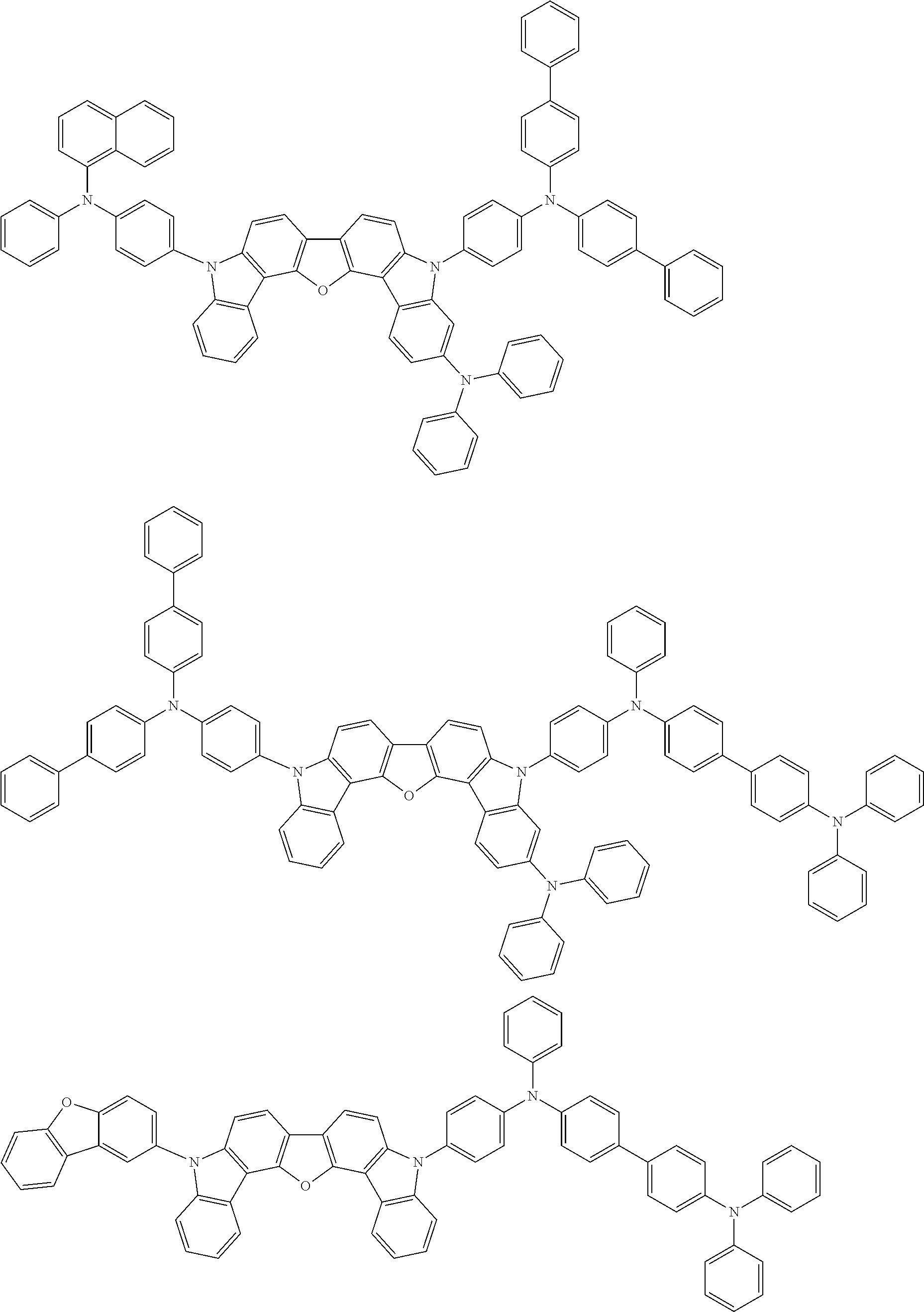


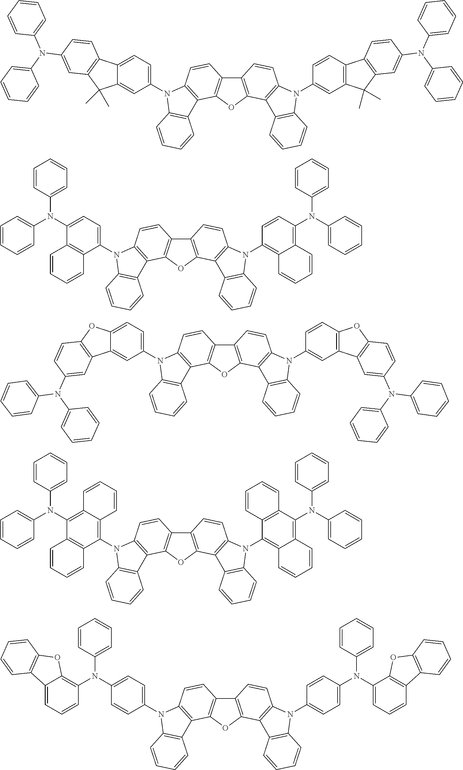


[Material for an Organic EL Device]
The compound represented by the formula (1) of the invention can be preferably used as a material for an organic EL device.
The material for an organic EL device according to one aspect of the invention comprises the compound represented by the formula (1) and is preferably used as a material for a hole-transporting layer that is adjacent to the emitting layer.
In the invention, the “material for a hole-transporting layer (hereinafter referred to as a hole-transporting material)” means a material that is used in a hole-transporting zone having one or more organic thin film layers. As the organic thin film layers of the hole-transporting zone, a hole-transporting layer, a hole-injecting layer, an electron-blocking layer or the like can be given.
The material for an organic EL device according to one aspect of the invention may contain only the compound represented by the formula (1) of the invention, and may contain other materials in addition to the compound represented by the formula (1) of the invention.
[Organic EL Device]
An explanation will be made on an organic EL device according to one aspect of the invention.
A first organic EL device of the invention comprises, between an anode and a cathode, one or more organic thin film layers including an emitting layer. At least one layer of the organic thin film layers comprises the material for an organic EL device or the hole-transporting material for an organic EL device of the invention.
A second organic EL device of the invention comprises, between an anode and a cathode, one or more organic thin film layers including an emitting layer, and a hole-transporting zone between the anode and the emitting layer, and the hole-transporting zone comprises the material for an organic EL device of the invention or the hole-transporting material for an organic EL device.
In the second organic EL device of the invention, it is preferred that the hole-transporting zone be adjacent to the emitting layer.
A third organic EL device of the invention comprises, between an anode and a cathode, one or more organic thin film layers including an emitting layer, and an electron-transporting zone between the cathode and the emitting layer, and the electron-transporting zone comprises the material for an organic EL device or the hole-transporting material for an organic EL device of the invention.
In the first to third organic EL devices of the invention, it is preferred that the emitting layer comprise the material for an organic EL device of the invention.
An organic EL device 1 has a structure in which, on a substrate 10, an anode 20, a hole-transporting zone 30, a phosphorescent emitting layer 40, an electron-transporting zone 50 and a cathode 60 are stacked in this sequence. The hole-transporting zone 30 means a hole-transporting layer, a hole-injecting layer, an electron-blocking layer or the like. Similarly, the electron-transporting zone 50 means an electron-transporting layer, an electron-injecting layer, a hole-blocking layer or the like. These layers may not be necessarily formed, but it is preferred that one or more layers be formed. In this device, the organic thin film layers mean organic layers provided in the hole-transporting zone 30, and the phosphorescent emitting layer 40 and organic layers provided in the electron-transporting zone 50. Among these organic thin film layers, at least one layer comprises the material for an organic EL device of the invention or one or more layers of the hole-transporting zone 30 comprise the hole-transporting material for an organic EL device of the invention. Due to this configuration, an organic EL device can emit light efficiently.
The content of the compound represented by the formula (1) relative to the organic thin film layer that comprises the material for an organic EL device of the invention is preferably 1 to 100 wt %. Similarly, the content of the compound represented by the formula (2) relative to any layer in the hole-transporting zone that comprises the hole-transporting material for an organic EL device of the invention is preferably 1 to 100 wt %.
In the organic EL device according to one aspect of the invention, it is preferred that the phosphorescent emitting layer 40 comprises the material for an organic EL device of the invention. It is more preferred that the material for an organic EL device of the invention be used as a host material of the emitting layer. Since the material of the invention has a sufficiently large triplet energy, even when a blue-emitting phosphorescent dopant material is used, the triplet energy of the phosphorescent dopant material can be efficiently confined in the emitting layer. Not only in the blue-emitting layer, the material for an organic EL device of the invention can be used in an emitting layer that emits light of a longer wavelength (green to red, or the like). However, it is preferable to use the material for an organic EL device in the blue-emitting layer.
The phosphorescent emitting layer comprises a phosphorescent emitting material (phosphorescent dopant). As the phosphorescent dopant, a metal complex compound can be given. Preferable is a compound that comprises a metal atom selected from Ir, Pt, Os, Au, Cu, Re and Ru and a ligand. It is preferred that the ligand have an ortho-metalated bond.
In respect of high phosphorescent quantum yield and capability of further improving the external quantum efficiency of the emitting device, it is preferred that the phosphorescent dopant be a compound that contains a metal atom selected from Ir, Os and Pt. A metal complex such as an iridium complex, an osmium complex and a platinum complex is further preferable. Among these, an iridium complex and a platinum complex are more preferable, with an ortho-metalated iridium complex being most preferable. The dopant may be used alone or in a mixture of two or more.
Although the concentration of the phosphorescent dopant in the phosphorescent emitting layer is not particularly restricted, it is preferably 0.1 to 40 weight % (wt %), and more preferably 0.1 to 30 weight % (wt %).
It is preferred that the material for an organic EL device or the invention be used in the organic thin film layers adjacent to the phosphorescent emitting 40. For example, when a layer that comprises the material of the invention (adjacent layer near to the anode) is formed between the phosphorescent emitting layer 40 and the hole-transporting zone 30, the layer functions an electron-barrier layer or an exciton-blocking layer.
The barrier layer (blocking layer) has a function of blocking movement of carriers or blocking of diffusion of excitons. An organic layer that serves to prevent leakage of electrons from the emitting layer to the hole-transporting zone may mainly be defined as an electron-barrier layer, and the organic layer that serves to prevent leakage of holes from the emitting layer to the electron-transporting zone may be defined as the hole-barrier layer. An organic layer that serves to prevent diffusion of triplet excitons generated in the emitting layer to peripheral layers of which the level of the triplet energy is lower than that of the emitting layer may be defined as an exciton-blocking layer (triplet barrier layer).
Further, the material for an organic EL device according to one aspect of the invention may be used in an organic thin film layer that is adjacent to the phosphorescent emitting layer 40 and also in another organic thin film layer that is in contact with the adjacent organic thin film layer.
In addition to the embodiments mentioned above, the organic EL device according to one aspect of the invention may take various known configurations. Further, emission from the emitting layer can be outcoupled from the anode, the cathode and both of the anode and the cathode.
In the organic EL device according to one aspect of the invention, it is preferred that at least any one of an electron-donating dopant and an organic metal complex be added to an interfacial region between the cathode and the organic thin film layer. Due to such a configuration, the luminance can be improved or the life can be prolonged in the organic EL device.
As the electron-donating dopant, at least one selected from an alkali metal, an alkali metal compound, an alkaline earth metal, an alkaline earth metal compound, a rare earth metal, a rare each metal compound or the like can be given.
As the organic metal complex, at least one selected from an organic metal complex containing an alkali metal, an organic metal complex containing an alkaline earth metal and an organic metal complex containing a rare earth metal or the like can be given.
As the alkali metal, lithium (Li) (work function: 2.93 eV), sodium (Na) (work function: 2.36 eV), potassium (K) (work function: 2.28 eV), rubidium (Rb) (work function: 2.16 eV), cesium (Cs) (work function: 1.95 eV) or the like can be given. An alkali metal having a work function of 2.9 eV or less is particularly preferable. Among these, K, Rb and Cs are preferable. Rb or Cs is further preferable, with Cs being most preferable.
As the alkaline earth metal, calcium (Ca) (work function: 2.9 eV), strontium (Sr) (work function: 2.0 eV to 2.5 eV), barium (B) (work function: 2.52 eV) or the like can be given. One having a work function of 2.9 eV or less is particularly preferable.
As the rare-earth metal, scandium (Sc), yttrium (Y), cerium (Ce), terbium (Tb), ytterbium (Yb) and the like can be given. One having a work function of 2.9 eV or less is particularly preferable.
Among the above-mentioned metals, the preferable metals have a particularly high reducing ability, and hence can provide the resulting organic EL device with improved luminance or a prolonged lifetime by adding a relatively small amount thereof to an electron-injecting region.
Examples of the alkali metal compound include an alkali oxide such as lithium oxide (Li2O), cesium oxide (Cs2O) or potassium oxide (K2O), and an alkali halide such as lithium fluoride (LiF), sodium fluoride (NaF), cesium fluoride (CsF) or potassium fluoride (KF). Among these, lithium fluoride (LiF), lithium oxide (Li2O) and sodium fluoride (NaF) are preferable.
Examples of the alkaline-earth metal compound include barium oxide (BaO), strontium oxide (SrO), calcium oxide (CaO), and mixtures thereof such as barium strontium acid (BaxSr1-xO) (0<x<1) and barium calcium acid (BaxCa1-x) (0<x<1). Among these, BaO, SrO and CaO are preferred.
Examples of the rare-earth metal compound include ytterbium fluoride (YbF3), scandium fluoride (ScF3), scandium oxide (ScO3), yttrium oxide (Y2O3), cerium oxide (Ce2O3), gadolinium fluoride (GdF3) and terbium fluoride (TbF3). Among these, YbF3, ScF3 and TbF3 are preferable.
The organic metal complexes are not particularly limited as long as they each contain, as a metal ion, at least one of alkali metal ions, alkaline-earth metal ions, and rare-earth metal ions, as mentioned above. Meanwhile, preferred examples of the ligand include, but are not limited to, quinolinol, benzoquinolinol, acridinol, phenanthridinol, hydroxyphenyloxazole, hydroxyphenytthiazole, hydroxydiaryloxadiazole, hydroxydiarylthiadiazole, hydroxyphenylpyridine, hydroxyphenylbenzimidazole, hydroxybenzotriazole, hydroxyfluborane, bipyridyl, phenanthroline, phthalocyanine, porphyrin, cyclopentadiene, β-diketones, azomethines, and derivatives thereof.
Regarding the addition form of the electron-donating dopant and the organic metal complex, it is preferred that the electron-donating dopant and the organic metal complex be formed in the shape of a layer or an island in the interfacial region. A preferred method for the formation is a method in which an organic substance as a light emitting material or an electron-injecting material for forming the interfacial region is deposited simultaneously with deposition of at least one of the electron-donating dopant and the organic metal complex by a resistant heating deposition method, thereby dispersing at least one of the electron-donating dopant and the organic metal complex reducing dopant in the organic substance. The dispersion concentration by molar ratio of the organic substance to the electron-donating dopant and/or the organic metal complex is normally 100:1 to 1:100, preferably 5:1 to 1:5.
In a case where at least one of the electron-donating dopant and the organic metal complex is formed into the shape of a layer, the light-emitting material or the electron-injecting material which serves as an organic layer in the interface is formed into the shape of a layer. After that, at least one of the electron-donating dopant and the organic metal complex is solely deposited by the resistant heating deposition method to form a layer preferably having a thickness of 0.1 nm to 15 nm.
In a case where at least one of the electron-donating dopant and the organic metal complex is formed into the shape of an island, the light-emitting material or the electron-injecting material which serves as an organic layer in the interface is formed into the shape of an island. After that, at least one of the electron-donating dopant and the organic metal complex is solely deposited by the resistant heating deposition method to form an island preferably having a thickness of 0.05 to 1 nm.
In addition, the ratio of the main component (emitting material or electron-injecting material) to at least one of the electron-donating dopant and the organic metal complex in the organic EL device according to one aspect of the invention (main component electron-donating dopant and/or organic metal complex) is preferably 5:1 to 1:5, more preferably 2:1 to 1:2 in terms of molar ratio.
In the organic EL device of the invention according to one aspect of the invention, configurations of other layers than those in which the above-mentioned material for an organic EL device of the invention is used are not particularly restricted, and known materials or the like can be used. Hereinbelow, a brief explanation will be made on the layer of the device of the embodiment 1. However, materials to be applied to the organic EL device of the invention are not limited to those mentioned below.
[Substrate]
As the substrate, a glass plate, a polymer plate or the like can be used.
Examples of materials of the glass plate include soda lime glass, barium-strontium-containing glass, lead glass, aluminosilicate glass, borosilicate glass, barium borosilicate glass, quartz, and the like.
Examples of materials of the polymer plate include polycarbonate, acryl, polyethylene terephthalate, polyethersulfone, polysulfone, and the like.
[Anode]
The anode is formed of a conductive material, for example. A conductive material having a work function larger than 4 eV is suitable.
As the conductive material, carbon, aluminum, vanadium, iron, cobalt, nickel, tungsten, silver, gold, platinum, palladium or the like, alloys thereof, an oxidized metal such as tin oxide and indium oxide used in an ITO substrate and a NESA substrate and further an organic conductive resin such as polythiophene and polypyrrole can be given.
If necessary, the anode may be formed of two or more layers.
[Cathode]
The cathode is formed of a conductive material, for example. A conductive material having a work function smaller than 4 eV is suitable.
As the conductive material, magnesium, calcium, tin, lead, titanium, yttrium, lithium, ruthenium, manganese, aluminum, lithium fluoride or the like, and alloys thereof can be given. The conductive material is not limited thereto.
As the alloy, a magnesium/silver alloy, a magnesium/indium alloy, a lithium/aluminum alloy or the like can be given as representative examples. The alloys are not limited thereto. The amount ratio of metals forming an alloy is controlled by the temperature of a deposition source, the atmosphere, the degree of vacuum or the like, and an appropriate ratio is selected.
If necessary, the cathode may be formed of two or more layers. The cathode can be formed by forming a thin layer from the above-mentioned conductive material by a method such as deposition, sputtering or the like.
When outcoupling light from the emitting layer through the cathode, it is preferable that the cathode have a light transmittance of more than 10%.
The sheet resistance of the cathode is preferably several hundred 0/square or less. The thickness of the cathode is normally 10 nm to 1 μm, and preferably 50 to 200 nm.
[Emitting Layer]
When a phosphorescent emitting layer is formed by using materials other than the material for an organic EL device of the invention, materials which are known as a material for a phosphorescent emitting layer can be used. Specifically, reference can be made to WO2005-079118 or the like.
The organic EL device according to one aspect of the invention may comprise a fluorescent emitting layer 70 as in the case of the device shown in FIG. 2 instead of the phosphorescent emitting layer 40 of the device shown in FIG. 1 . As the fluorescent emitting layer, known materials can be used.
The emitting layer can be of a double-host (often referred to as host/co-host) type. Specifically, in the emitting layer, an electron-transporting host and a hole-transporting host may be combined to control the carrier balance therein.
The emitting layer also may be of a double-dopant type. By incorporating two or more kinds of dopant materials having a high quantum yield to the emitting layer, each dopant emits light. For example, there may be a case that a yellow emitting layer is realized by co-depositing a host, and a red dopant and a green dopant.
The emitting layer may be a single layer or may have a stacked layer structure. When the emitting layers are stacked, due to accumulation of electrons and holes in the interface of the emitting layer, the recombination region may be concentrated in the emitting layer interface, whereby the quantum efficiency is improved.
[Hole-Injecting Layer and Hole-Transporting Layer]
A hole-injecting layer and transporting layer is a layer that helps holes to be injected to an emitting layer and to be transported to an emitting region. It has a large hole mobility and a small ionization energy.
As the material for a hole-injecting and transporting layer, a material that transports holes to the emitting layer at a lower electric field is preferable. Further, it is preferred that the material have a mobility of holes of at least 10−4 cm2/V sec when an electric field of 104 to 106 V/cm is applied.
[Electron-Injecting Layer and Electron-Transporting Layer]
The electron-injecting and transporting layer helps electrons to be injected to an emitting layer and to be transported to an emitting region. It has a large electron mobility.
In the organic EL device, it is known that since emitted light is reflected by an electrode (a cathode, for example), emission outcoupled directly from an anode interferes with emission outcoupled after being reflected by the electrode. In order to utilize the interference effect efficiently, the film thickness of the electron-injecting and transporting layer is appropriately selected to be several nm to several μm. When the film thickness is large, in particular, it is preferred that the electron mobility be at least 10−5 cm2/Vs or more at an applied electric field intensity of 104 to 106 V/cm in order to avoid an increase in voltage.
As the electron-transporting material used in the electron-injecting and transporting layer, an aromatic heterocyclic compound containing one or more hetero atoms in the molecule is preferably used, with a nitrogen-containing ring derivative being particularly preferable. Further, as the nitrogen-containing ring derivative, an aromatic ring compound having a nitrogen-containing 6-membered ring or 5-membered ring skeleton, or a fused aromatic ring compound having a nitrogen-containing 6-membered ring or 5-membered ring skeleton is preferable. Examples thereof include compounds containing a pyridine ring, a pyrimidine ring, a triazine ring, a benzimidazole ring, a phenanthroline ring, a quinazoline ring or the like in the skeleton.
In addition, an organic layer with a semiconductor property may be formed by doping a donor material (n) or doping an acceptor material (p). Representative examples of N-doping include one in which an electron-transporting material is doped with a metal such as Li or Cs. Representative examples of P-doping include one in which a hole-transporting material is doped with an acceptor material such as F4TCNQ (see Japan Patent No. 3695714, for example).
Each layer of the organic EL device according to one aspect of the invention can be formed by using known methods including the dry-type film formation such as vacuum deposition, sputtering, plasma coating, ion-plating or the like and the wet-type film formation such as spin coating, dipping, flow coating or the like.
The film thickness of each layer is not particularly limited, but should be set to be a proper thickness. If the film thickness is too large, a large voltage is required to be applied in order to obtain a certain light output, thereby leading to lowering in efficiency. If the film thickness is too small, due to generation of pinholes or the like, a sufficient luminance cannot be obtained when an electric field is applied. Normally, the film thickness is preferably 5 nm to 10 μm, and a range of 10 nm to 0.2 μm is further preferable.
An organic EL device obtained by using a material for an organic EL device that comprises the compound of the invention and/or the hole-transporting material for an organic EL device of the invention can be used in an electric equipment such as a display component including an organic EL panel module, a display apparatus such as a TV, a mobile phone or a personal computer and an emitting apparatus such as lightings, lights for vehicles or the like.
The invention will be explained in more detail in accordance with the Synthesis Examples and the Examples, which should not be construed as limiting the scope of the invention.
(1) Synthesis of Compound (1-1)

In a three-neck flask, 20.0 g (80.9 mmol) of dibenzofuran and 200 ml of dehydrated tetrahydrofuran were placed. In a nitrogen atmosphere, the reactor was cooled to −70° C. To the reactor, 53 ml (88.9 mmol) of a 1.68M s-butyllithium hexane solution was added dropwise, and the resultant was stirred at −70° C. for 1 hour. 37.3 ml (162 mmol) of triisopyl borate was added, and stirred at room temperature for 6 hours. After completion of the reaction, 100 ml of a 1N HCL aqueous solution was added, and stirred for 30 minutes. A sample solution was transferred to a dropping funnel, and extracted several times with dichloromethane. The extracted product was dried with anhydrous magnesium sulfate, filtered and concentrated. The concentrated product was washed by dispersing in hexane, whereby white solids were obtained.
The yield was 15.9 g and the percentage yield was 93%.
(2) Synthesis of Compound (1-2)

In a three-neck flask, 25.0 g (97.7 mmol) of compound (1-1), 74.7 g (300 mmol) of 2-iodonitrobenzene, 250 mL of a 2M aqueous solution of sodium carbonate, 500 mL of 1,2-dimethoxyethane and 2.30 g (1.95 mmol) of Pd(PPh3)4 were placed, and the mixture was refluxed in a nitrogen atmosphere for 12 hours. After completion of the reaction, the sample solution was filtered, and the obtained solids were washed with methanol and hexane.
The yield was 26.5 g and the percentage yield was 66%.
(3) Synthesis of Compound (1-3)

In a three-neck flask, 26.5 g (64.6 mmol) of compound (1-2) and 430 ml of triethyl phosphite were placed, and the mixture was refluxed with heating at 170° C. for 16 hours.
After completion of the reaction, distillation was conducted, thereby to remove the remaining triethyl phosphite and triethyl phosphite residues. The obtained organic phase was purified by silica gel chromatography (hexane:dichloromethane:10:1 to 5:1 to 1:1), whereby pale yellow solids were obtained.
The yield was 12.1 g and the percentage yield was 54%.
(4) Synthesis of Compound (1-4)

In a three-neck flask, 3.46 g (10 mmol) of compound (1-3), 2.04 g (10 mmol) of iodobenzene, 1.90 g (10 mmol) of copper iodide, 4.24 g (20 mmol) of tripotassium phosphate, 2.28 g (20 mmol) of cyclohexadiamine and 30 mL of 1,4-dioxane were placed. The mixture was refluxed for 12 hours in a nitrogen atmosphere.
After completion of the reaction, insoluble matters were removed by filtration through celite. The filtrate was transferred to a dripping funnel, and extracted several times with dichloromethane. The obtained organic phase was dried with anhydrous magnesium sulfate, filtered and concentrated. The concentrated product was purified by silica gel chromatography (hexane:dichloromethane=10:1 to 5:1), whereby white solids were obtained.
The yield was 3.38 g and the percentage yield was 40%.
(5) Synthesis of Compound (1)

In a three-neck flask, 2.11 g (5 mmol) of compound (1-4), 1.78 g (5.5 mmol) of 4-bromotriphenylamine, 0.95 g (5 mmol) of copper iodide, 2.12 g (10 mmol) of potassium triphosphate, 1.14 g (10 mmol) of cyclohexanediamine and 20 mL of 1,4-dioxane were placed. The mixture was refluxed in a nitrogen atmosphere for 12 hours.
After completion of the reaction, insoluble matters were removed by filtration through celite. The filtrate was transferred to a dripping funnel, and extracted several times with toluene. The obtained organic phase was dried with anhydrous magnesium sulfate, filtered and concentrated. The concentrated product was purified by silica gel chromatography (hexane:toluene=7:3), whereby white solids were obtained.
The yield was 2.16 g and the percentage yield was 65%.
As a result of a FD-MS analysis, m/e was 665 relative to the molecular weight of 665. The measurement results of 1H-NMR are shown below.
1H-NMR (400 MHz, CDCl3) δ7.07-7.12 (2H, m), 7.22-7.40 (10H, m), 7.43-7.53 (11H, m), 7.63-7.70 (4H, m), 7.94-7.99 (2H, m), 8.75-8.79 (2H, m)

In a three-neck flask, 2.11 g (5 mmol) of compound (1-4), 2.20 g (5.5 mmol) of N-(4-bromophenyl)-N-(4-biphenyl)aniline, 0.95 g (5 mmol) of copper iodide, 2.12 g (10 mmol) of potassium triphosphate, 1.14 g (10 mmol) of cyclohexanediamine and 20 mL of 1,4-dioxane were placed. The mixture was refluxed in a nitrogen atmosphere for 18 hours.
After completion of the reaction, insoluble matters were removed by filtration through celite. The filtrate was transferred to a dripping funnel and extracted several times with toluene. The obtained organic phase was dried with anhydrous magnesium sulfate, filtered and concentrated. The resultant was purified by silica gel chromatography (hexane:toluene=3:1), whereby white solids were obtained.
The yield was 2.60 g and the percentage yield was 70%.
As a result of a FD-MS analysis, m/e was 741 relative to the molecular weight of 741.
The measurement results of 1H-NMR are shown below.
1H-NMR (400 MHz, CDCl3) δ7.11-7.18 (2H, m), 7.21-7.39 (9H, m), 7.41-7.69 (20H, m), 7.98-8.03 (2H, m), 8.76-8.79 (2H, m)

In a three-neck flask, 2.11 g (5 mmol) of compound (1-4), 1.78 g (5.5 mmol) of 3-bromotriphenylamine, 90 mg (0.1 mmol) of Pd2(dba)3, 0.12 g (0.4 mmol) of tri-t-butylphosphonium tetrafluoroborate, 0.67 g (7 mmol) of sodium t-butoxide and 30 mL of dehydrated toluene were placed. The resultant was refluxed in an argon atmosphere for 12 hours.
After completion of the reaction, insoluble matters were separated by filtration through celite. The filtrate was transferred to a dripping funnel and extracted several times with toluene. The obtained organic phase was dried with anhydrous magnesium sulfate, filtered and concentrated. The resultant was purified by silica gel chromatography (hexane:toluene=5:2), whereby white solids were obtained.
The yield was 2.40 g and the percentage yield was 72%.
As a result of a FD-MS analysis, m/e was 665 relative to the molecular weight of 665.

In a three-neck flask, 2.11 g (5 mmol) of compound (14), 2.06 g (5.5 mmol) of N-(4-bromophenyl)-N-(1-naphthyl)aniline, 90 mg (0.1 mmol) of Pd2(dba)3, 0.12 g (0.4 mmol) of tri-t-butylphosphonium tetrafluoroborate, 0.67 g (7 mmol) of sodium t-butoxide and 30 mL of dehydrated toluene were placed. The resultant was refluxed for 24 hours in an argon atmosphere.
After completion of the reaction, insoluble matters were separated by filtration through celite. The filtrate was transferred to a dripping funnel and extracted several times with toluene. The obtained organic phase was dried with anhydrous magnesium sulfate, filtered and concentrated. The resultant was purified by silica gel chromatography (hexane:toluene=4:1), whereby white solids were obtained.
The yield was 3.15 g and the percentage yield was 88%.
As a result of a FD-MS analysis, m/e was 715 relative to the molecular weight of 715.

In a three-neck flask, 2.11 g (5 mmol) of compound (1-4), 2.20 g (5.5 mmol) of 4-bromo-4′-(diphenylamino)biphenyl, 90 mg (0.1 mmol) of Pd2(dba)3, 0.12 g (0.4 mmol) of tri-t-butylphosphonium tetrafluoroborate, 0.67 g (7 mmol) of sodium t-butoxide and 30 mL of dehydrated toluene were plated. The resultant was refluxed for 36 hours in an argon atmosphere.
After completion of the reaction, insoluble matters were separated by filtration through celite. The filtrate was transferred to a dripping funnel and extracted several times with toluene. The obtained organic phase was dried with anhydrous magnesium sulfate, filtered and concentrated. The concentrated product was purified by silica gel chromatography (hexane:toluene=2:1), whereby white solids were obtained.
The yield was 3.15 g and the percentage yield was 85%.
As a result of a FD-MS analysis, m/e was 741 relative to the molecular weight of 741.

In a three-neck flask, 2.11 g (5 mmol) of compound (1-4), 2.20 g (5.5 mmol) of 4-bromo-4′-[N-phenyl-N-(1-naphthyl)amino]biphenyl, 90 mg (0.1 mmol) of Pd2(dba)3, 0.12 g (0.4 mmol) of tri-t-butylphosphonium tetrafluoroborate, 0.67 g (7 mmol) of sodium t-butoxide and 30 mL of dehydrated toluene were placed. The resultant was refluxed for 36 hours in an argon atmosphere.
After completion of the reaction, insoluble matters were separated by filtration. The filtrate was transferred to a dripping funnel and extracted several times with toluene. The obtained organic phase was dried with anhydrous magnesium sulfate, filtered and concentrated. The resultant was purified by silica gel chromatography (hexane:toluene=2:1), whereby white solids were obtained.
The yield was 2.45 g and the percentage yield was 62%.
As a result of a FD-MS analysis, m/e was 791 relative to the molecular weight of 791.
(1) Synthesis of Compound (7-1)

In a three-neck flask, 34.6 g (100 mmol) of compound (1-3), 24.7 g (100 mmol) of 2-bromodibenzofuran, 19.0 g (100 mmol) of copper iodide, 21.2 g (100 mmol) of potassium triphosphate, 5.9 g (50 mmol) of cyclohexanediamine and 500 mL of dehydrated 1,4-dioxane were placed. The resultant was refluxed for 48 hours in an argon atmosphere.
After completion of the reaction, insoluble matters were separated by filtration through celite. The filtrate was transferred to a dripping funnel and extracted several times with toluene. An organic phase obtained was dried with anhydrous magnesium sulfate, filtered and concentrated. The resultant was purified by silica gel chromatography (hexane:toluene=10:1 to 5:1 to 2:1), whereby compound (7-1) as white solids was obtained.
The yield was 11.8 g and the percentage yield was 23%.
(2) Synthesis of Compound (7)

In a three-neck flask, 2.56 g (5 mmol) of compound (7-1), 1.78 g (5.5 mmol) of 3-bromotriphenylamine, 90 mg (0.1 mmol) of Pd2(dba)3, 0.12 g (0.4 mmol) of tri-t-butylphosphonium tetrafluoroborate, 0.67 g (7 mmol) of sodium t-butoxide and 30 mL of dehydrated toluene were placed. The resultant was refluxed in an argon atmosphere for 20 hours.
After completion of the reaction, insoluble matters were separated by filtration through celite. The filtrate was transferred to a dripping funnel and extracted several times with toluene. An organic phase obtained was dried with anhydrous magnesium sulfate, filtered and concentrated. The resultant was purified by silica gel chromatography (hexane:toluene=3:1), whereby white solids were obtained.
The yield was 2.83 g and the percentage yield was 75%.
As a result of a FD-MS analysis, m/e was 755 relative to the molecular weight of 755.

In a three-neck flask, 2.11 g (5 mmol) of compound (1-4), 2.20 g (5.5 mmol) of 4-bromo-4′-[N-phenyl-N-(2-naphthyl)amino]biphenyl, 90 mg (0.1 mmol) of Pd2(dba)3, 0.12 g (0.4 mmol) of tri-t-butylphosphonium tetrafluoroborate, 0.67 g (7 mmol) of sodium t-butoxide and 30 mL of dehydrated toluene were placed. The resultant was refluxed in an argon atmosphere for 36 hours.
After completion of the reaction, insoluble matters were separated by filtration through celite. The filtrate was transferred to a dripping funnel and extracted several times with toluene. An organic phase obtained was dried with anhydrous magnesium sulfate, filtered and concentrated. The resultant was purified by silica gel chromatography (hexane:toluene=2:1), whereby white solids were obtained.
The yield was 3.64 g and the percentage yield was 92%.
As a result of a FD-MS analysis, m/e was 791 relative to the molecular weight of 791.

In a three-neck flask, 2.11 g (5 mmol) of compound (1-4), 2.42 g (5.5 mmol) of 2-bromo-7-(diphenylamino)-9,9′-dimethylfluorene, 90 mg (0.1 mmol) of Pd2(dba)3, 0.12 g (0.4 mmol) of tri-t-butylphosphonium tetrafluoroborate, 0.67 g (7 mmol) of sodium t-butoxide and 30 mL of dehydrated toluene were placed. The resultant was refluxed in an argon atmosphere for 12 hours.
After completion of the reaction, insoluble matters were separated by filtration through celite. The filtrate was transferred to a dripping funnel and extracted several times with toluene. The organic phase obtained was dried with anhydrous magnesium sulfate, filtered and concentrated. The concentrated product was purified by silica gel chromatography (hexane:toluene=3:2), whereby white solids were obtained.
The yield was 1.95 g and the percentage yield was 50%.
As a result of a FD-MS analysis, m/e was 781 relative to the molecular weight of 781.
(1) Synthesis of Compound (10-1)

In a three-neck flask, 15.0 g (60.7 mmol) of 4-bromobenzofuran, 11.3 g (121 mmol) of aniline, 0.83 g (0.91 mmol) of Pd2(dba)3, 1.13 g (1.81 mmol) of rac-BINAP, 11.6 g (120.7 mmol) of sodium t-butoxide and 300 mL of dehydrated xylene were placed. The resultant was refluxed in an argon atmosphere for 8 hours.
After completion of the reaction, insoluble matters were separated by filtration through celite. The filtrate was transferred to a dripping funnel and extracted several times with toluene. The obtained organic phase was dried with anhydrous magnesium sulfate, filtered and concentrated. The concentrated product was purified by silica gel chromatography (hexane:toluene=4:1), whereby white solids were obtained.
The yield was 12.1 g and the percentage yield was 77%.
(2) Synthesis of Compound (10-2)

In a three-neck flask, 5.19 g (20 mmol) of compound (10-1), 5.66 g (20 mmol) of 4-bromoiodobenzene, 3.80 g (20 mmol) of copper iodide, 8.48 g (40 mmol) of potassium triphosphate, 4.56 g (40 mmol) of cyclohexanediamine and 60 mL of 1,4-dioxane were placed. The resultant was refluxed in an argon atmosphere for 30 hours.
After completion of the reaction, insoluble matters were separated by filtration through celite. The filtrate was transferred to a dripping funnel and extracted several times with toluene. An organic phase obtained was dried with anhydrous magnesium sulfate, filtered and concentrated. The resultant was purified by silica gel chromatography (hexane:toluene=4:1), whereby white solids were obtained.
The yield was 2.32 g and the percentage yield was 28%.
(3) Synthesis of Compound (10)

In a three-neck flask, 2.11 g (5 mmol) of compound (1-4), 2.28 g (5.5 mmol) of compound (10-2), 90 mg (0.1 mmol) of Pd2(dba)3, 0.12 g (0.4 mmol) of tri-t-butylphosphonium tetrafluoroborate, 0.67 g (7 mmol) of sodium t-butoxide and 30 mL of dehydrated toluene were placed. The resultant was refluxed in an argon atmosphere for 48 hours.
After completion of the reaction, insoluble matters were separated by filtration through celite. The filtrate was transferred to a dripping funnel and extracted several times with toluene. The obtained organic phase was dried with anhydrous magnesium sulfate, filtered and concentrated. The concentrated product was purified by silica gel chromatography (hexane:toluene=3:2), whereby white solids were obtained.
The yield was 1.32 g and the percentage yield was 35%.
As a result of a FD-MS analysis, m/e was 755 relative to the molecular weight of 755.
(1) Synthesis of Compound (11-1)

In a three-neck flask, 25.7 g (100 mmol) of intermediate (A) (synthesized according to the method described in WO2009/148015), 21.4 g (105 mmol) of iodobenzene, 19.0 g (100 mmol) of copper iodide, 42.5 g (200 mmol) of potassium triphosphate, 22.8 g (200 mmol) of cyclohexanediamine and 200 mL of dehydrated 1,4-dioxane were placed. The mixture was refluxed in an argon atmosphere for 12 hours.
After completion of the reaction, insoluble matters were separated by filtration through celite. The filtrate was transferred to a dripping funnel and extracted several times with toluene. An organic phase obtained was dried with anhydrous magnesium sulfate, filtered and concentrated. The resultant was purified by silica gel chromatography (hexane:toluene=7:3), whereby white solids were obtained.
The yield was 21.7 g and the percentage yield was 65%.
(2) Synthesis of Compound (11-2)

In a three-neck flask, 21.7 g (65 mmol) of compound (11-1) and 400 mL of dehydrated tetrahydrofuran were placed, and cooled to −70° C. in an argon atmosphere. Subsequently, 47 mL of 1.4M sec-butyllithium (hexane-cyclohexane solution) was added dropwise to the reaction solution. After stirring for 2 hours, 36.7 g (195 mmol) of triisopropyl borate was added. After returning to room temperature and stirring was conducted for 3 hours, the reaction solution was concentrated. To residues obtained, dichloromethane and 2N hydrochloric acid were added, followed by stirring for 2 hours, and an organic phase was separated. Solids obtained by concentrating the organic phase were washed with toluene, whereby white solids were obtained.
The yield was 17.2 g and the percentage yield was 70%.
(3) Synthesis of Compound (11-3)

In a three-neck flask, 17.0 g (45 mmol) of compound (11-2), 10.7 g (45 mmol) of 2-bromo-4-chloronitrobenzene, 1.56 g (1.35 mmol) of Pd(PPh3)4, 60 mL of an aqueous 2M sodium carbonate solution and 200 mL of 1,2-dimethoxyethane (DME) were placed. The resultant was refluxed in an argon atmosphere for 24 hours.
After completion of the reaction, insoluble matters were separated by filtration through celite. The filtrate was transferred to a dripping funnel and extracted several times with dichloromethane. An organic phase obtained was dried with anhydrous magnesium sulfate, filtered and concentrated. The concentrated product was purified by silica gel chromatography (hexane:dichloromethane=7:3), whereby white solids were obtained.
The yield was 15.4 g and the percentage yield was 70%.
(4) Synthesis of Compound (11-4)

In a three-neck flask, 14.7 g (30 mmol) of compound (11-3), 23.6 g (90 mmol) of triphenylphosphine and 200 mL of o-dichlorobenzene were placed. The resultant was refluxed at 180° C. in an argon atmosphere for 24 hours.
After completion of the reaction, residues obtained by concentrating the reaction solution was purified by silica gel chromatography (hexane:dichloromethane=7:3→1:1), whereby white solids were obtained.
The yield was 8.9 g and the percentage yield was 65%.
(5) Synthesis of Compound (11-5)

In a three-neck flask, 6.9 g (15 mmol) of compound (11-4), 3.1 g (15 mmol) of iodobenzene, 2.9 g (15 mmol) of copper iodide, 6.4 g (30 mmol) of potassium triphosphate, 3.4 g (30 mmol) of cyclohexanediamine and 60 mL of dehydrated 1,4-dioxane were placed. The resultant was refluxed in an argon atmosphere for 24 hours.
After completion of the reaction, insoluble matters were separated by filtration through celite. The filtrate was transferred to a dripping funnel and extracted several times with toluene. An organic phase obtained was dried with anhydrous magnesium sulfate, filtered and concentrated. The resultant was purified by silica gel chromatography (hexane:toluene=2:1), whereby white solids were obtained.
The yield was 6.8 g and the percentage yield was 85%.
(6) Synthesis of Compound (11)

In a three-neck flask, 2.67 g (5 mmol) of compound (11-5), 1.35 g (5.5 mmol) of (N-phenyl)biphenylamine, 90 mg (0.1 mmol) of Pd2(dba)3, 0.12 g (0.4 mmol) of tri-t-butylphosphonium tetrafluoroborate, 0.67 g (7 mmol) of sodium t-butoxide and 30 mL of dehydrated xylene were placed. The resultant was refluxed for 48 hours in an argon atmosphere.
After completion of the reaction, insoluble matters were separated by filtration through celite. The filtrate was transferred to a dripping funnel and extracted several times with toluene. An organic phase obtained was dried with anhydrous magnesium sulfate, filtered and concentrated. The resultant was purified by silica gel chromatography (hexane:toluene=3:2), whereby white solids were obtained.
The yield was 1.89 g and the percentage yield was 51%.
As a result of a FD-MS analysis, m/e was 741 relative to the molecular weight of 741.

In a three-neck flask, 2.56 g (5 mmol) of compound (7-1), 1.78 g (5.5 mmol) of 4-bromotriphenylamine, 90 mg (0.1 mmol) of Pd2(dba)3, 0.12 g (0.4 mmol) of tri-t-butylphosphonium tetrafluoroborate, 0.67 g (7 mmol) of tri-t-sodium t-butoxide and 30 mL of dehydrated toluene were placed. The resultant was refluxed in an argon atmosphere for 28 hours.
After completion of the reaction, insoluble matters were separated by filtration through celite. The filtrate was transferred to a dripping funnel and extracted several times with toluene. An organic phase obtained was dried with anhydrous magnesium sulfate, and filtered and concentrated. The resultant was purified by silica gel chromatography (hexane:toluene=3:2), whereby white solids were obtained.
The yield was 2.44 g and the percentage yield was 64%.
As a result of a FD-MS analysis, m/e was 755 relative to the molecular weight of 755.
[Production and Evaluation of Organic EL Device]
A glass substrate with 130 nm-thick ITO electrode lines (manufactured by GEOMATEC Co., Ltd.) was subjected to ultrasonic cleaning in isopropyl alcohol for 5 minutes and then UV ozone cleaning for 30 minutes.
The cleaned glass substrate with ITO electrode lines was mounted on a substrate holder in a vacuum deposition apparatus. First, on the surface on which the ITO electrode lines had been formed, compound (HI1) was deposited by resistance heating so as to cover the ITO electrode lines to form a 20 nm-thick film, and subsequently compound (HT1) was deposited by resistance heating to form a 50 nm-thick film. The film-forming rate was 1 Å/s. These thin films function as a hole-injecting layer and a hole-transporting layer, respectively.
Next, on the hole-transporting layer, compound (2) was deposited by resistance heating to form a thin film (electron-barrier layer) with a film thickness of 10 nm.
Subsequently, on the electron-barrier layer, compound (H1) and compound (BD1) were simultaneously deposited by resistance heating to form a 40 nm-thick thin film. At this time, compound (BD1) was deposited such that the mass ratio of compound (BD1) became 20% relative to the total mass of compound (H1) and compound (BD1). The film forming rate was 1.2 Å/s for H1, and 0.3 Å/s for BD1. This thin film functions as a phosphorescent emitting layer.
Subsequently, on the phosphorescent emitting layer, compound (HB1) was deposited by resistance heating to form a 5 nm-thick thin film. The film forming rate was 1.2 Å/s. This thin film functions as a hole barrier layer.
Next, on the hole barrier layer, compound (ET1) was deposited by resistance heating to form a 25 nm-thick thin film. The film forming rate was 1 Å/s. This film functions as an electron-transporting layer.
Subsequently, on this electron-transporting layer, a LiF film having a thickness of 1.0 nm was deposited at a film-forming rate of 0.1 Å/s.
Next, on the LiF film, metal aluminum was deposited at a film forming rate of 8.0 Å/s to form a metal electrode having a film thickness of 80 nm, whereby an organic EL device was produced.
The materials used for the production of the organic EL device are shown below.


The fabricated organic EL device was caused to emit light by direct current driving to measure a luminance and a current density, whereby a voltage and a luminous efficiency (external quantum efficiency) at a current density of 1 mA/cm2 were obtained. Further, a LT70% luminance life (time that elapsed until the initial luminance was reduced to 70%) was measured at an initial luminance of 3000 cd/m2. The results of evaluation of these luminous performance are shown in Table 1.
Organic EL devices were produced and evaluated in the same manner as in Example 1, except that compounds (3) to (9) were used instead of compound (2). The results are shown in Table 1.
An organic EL device was produced and evaluated in the same manner as in Example 1, except that compound (13) was used instead of compound (2). The results are shown in Table 1.

An organic EL device was produced and evaluated in the same manner as in Example 1, except that compound (1) was used instead of compound (2). The results are shown in Table 1.
An organic EL device was produced and evaluated in the same manner as in Example 1, except that compound (12) was used instead of compound (2). The results are shown in Table 1.
| TABLE 1 | |||||
| LT70% | |||||
| Electron-barrier | Voltage | External quantum | luminous | ||
| layer material | (V) | efficiency (%) | time (hour) | ||
| Example 1 | Compound (2) | 4.4 | 23.4 | 205 |
| Example 2 | Compound (3) | 4.5 | 23.8 | 130 |
| Example 3 | Compound (4) | 4.5 | 21.7 | 163 |
| Example 4 | Compound (5) | 4.4 | 22.6 | 190 |
| Example 5 | Compound (6) | 4.5 | 21.7 | 231 |
| Example 6 | Compound (7) | 4.4 | 23.7 | 127 |
| Example 7 | Compound (8) | 4.4 | 21.4 | 180 |
| Example 8 | Compound (9) | 4.5 | 22.0 | 248 |
| Comp. Ex. 1 | Compound (13) | 4.4 | 22.9 | 78 |
| Comp. Ex. 2 | Compound (1) | 4.6 | 23.9 | 80 |
| Comp. Ex. 3 | Compound (12) | 4.4 | 21.9 | 79 |
As shown in Table 1, the compound of the invention can be used as a material for an electron-barrier layer (hole-transporting layer). In particular, organic EL devices shown in Examples 1 to 8 in which the compound of the invention was used as a material for the electron-barrier layer that is adjacent to the emitting layer had a significantly longer life as compared with the organic EL devices of Comparative Examples 1 to 3 without deteriorating the voltage and the efficiency.
A glass substrate with 130 nm-thick ITO electrode lines (manufactured by GEOMATEC Co., Ltd.) was subjected to ultrasonic cleaning in isopropyl alcohol for 5 minutes and then UV ozone cleaning for 30 minutes.
The cleaned glass substrate with ITO electrode lines was mounted on a substrate holder in a vacuum deposition apparatus. First, on the surface of the side on which the ITO electrode lines had been formed, compound (HI1) was deposited by resistance heating so as to cover the ITO electrode lines to form a 20 nm-thick film, and subsequently compound (HT1) was deposited by resistance heating to form a 60 nm-thick film sequentially. The film-forming rate was 1 Å/s. These thin films function as a hole-injecting layer and a hole-transporting layer, respectively.
Subsequently, on the hole-transporting layer, compound (7) and compound (BD1) were simultaneously deposited by resistance heating to form a 40 nm-thick thin film. At this time, compound (BD1) was deposited such that the mass ratio of compound (BD1) became 20% relative to the total mass of compound (7) and compound (BD1). The film forming rate was 1.2 Å/s for compound (7), and 0.3 Å/s for (BD1). This thin film functions as a phosphorescent emitting layer.
Subsequently, on the phosphorescent emitting layer, compound (HB1) was deposited by resistance heating to form a 5 nm-thick thin film. The film forming rate was 1.2 Å/s. This thin film functions as a hole-barrier layer.
Next, on the hole-barrier layer, compound (ET1) was deposited by resistance heating to form a 25 nm-thick thin film. The film forming rate was 1 Å/s. This film functions as an electron-transporting layer.
Subsequently, on this electron-injecting layer, a UF film having a thickness of 1.0 nm was deposited at a film-forming rate of 0.1 Å/s.
Next, on the LiF film, metal aluminum was deposited at a film forming rate of 8.0 Å/s to form a metal cathode having a film thickness of 80 nm, whereby an organic EL device was produced.
The thus fabricated organic EL device was driven by direct current driving to measure a luminance and a current density, whereby a voltage and a luminous efficiency (external quantum efficiency) at a current density of 1 mA/cm2 were obtained. The results of evaluation of these luminous performance are shown in Table 2.
An organic EL device was produced and evaluated in the same manner as in Example 9, except that compound (10) was used instead of compound (7). The results are shown in Table 2.
An organic EL device was produced and evaluated in the same manner as in Example 9, except that compound (13) was used instead of compound (7). The results are shown in Table 2.
| TABLE 2 | ||||
| Emitting layer host | Voltage | External quantum | ||
| material | (V) | efficiency (%) | ||
| Example 9 | Compound (7) | 4.0 | 18.6 |
| Example 10 | Compound (10) | 4.2 | 18.3 |
| Comp. Ex. 4 | Compound (13) | 4.4 | 17.6 |
As shown in Table 2, the compound of the invention can be used as a host material of the emitting layer. When compound (7) or compound (10) were used, improvement in efficiency could be confirmed as compared with the case of compound (13).
Although only some exemplary embodiments and/or examples of this invention have been described in detail above, those skilled in the art will readily appreciate that many modifications are possible in the exemplary embodiments and/or examples without materially departing from the novel teachings and advantages of this invention. Accordingly, all such modifications are intended to be included within the scope of this invention.
The documents described in this specification are incorporated herein by reference in its entirety.
Claims (23)
1. A compound represented by the following formula (1):

wherein in the formula (1),
X is O, S or a group represented by N-Ra;
Y1 to Y4 are independently N or a group represented by C-Ra;
Y5 and Y6 are independently N, a group represented by C-Ra or a carbon atom that is bonded to —N(Ar5)(Ar6);
Y7 and Y8 are independently N, a group represented by C-Ra or a carbon atom that is bonded to —N(Ar7)(Ar8);
Y9 to Y12 are independently N, a group represented by C-Ra or a carbon atom that is bonded to —N(Ar11)(Ar12);
Ar1 to Ar12 are independently a substituted or unsubstituted aromatic hydrocarbon group including 6 to 30 ring carbon atoms or a substituted or unsubstituted aromatic heterocyclic group including 3 to 30 ring atoms;
Ra is a hydrogen atom, a substituted or unsubstituted aromatic hydrocarbon group including 6 to 30 ring carbon atoms, a substituted or unsubstituted aromatic heterocyclic group including 3 to 30 ring atoms, a substituted or unsubstituted alkyl group including 1 to 30 carbon atoms, a substituted or unsubstituted fluoroalkyl group including 1 to 30 carbon atoms, a substituted or unsubstituted cycloalkyl group including 3 to 30 ring carbon atoms, a substituted or unsubstituted aralkyl group including 7 to 30 carbon atoms, a substituted phosphoryl group, a substituted silyl group, a cyano group, a nitro group or a carboxy group,
when plural Ras are present in the formula (1), the plural Ras may be the same or different from each other, and the plural Ras may form a ring;
when Ar1 is a p-phenylene group, Ar3 and Ar4 are not both an unsubstituted phenyl group;
when Ar2 is a p-phenylene group, Ar9 and Ar10 are not both an unsubstituted phenyl group;
a is an integer of 0, 1 or 2;
b is an integer of 0, 1 or 2;
c is an integer of 0, 1 or 2;
d is an integer of 0, 1 or 2;
e is an integer of 0, 1, 2, 3 or 4; and
a+b+c+d+e is 1 to 6.
2. The compound according to claim 1 , wherein, in the formula (1), at least one of a and d is 1.
3. The compound according to claim 1 , wherein, in the formula (1), a is 0, and b+c+d+e is 1 to 4.
4. The compound according to claim 1 , wherein, in the formula (1), e is 0 and a+b+c+d is 1 to 4.
5. The compound according to claim 1 , wherein, in the formula (1), a and d are 0 and b+c+e is 1 to 4.
6. The compound according to claim 1 , wherein, in the formula (1), a and e are 0 and b+c+d is 1 to 4.
7. The compound according to claim 1 , wherein, in the formula (1), a, d and e are 0 and b+c is 1 or 2.
8. The compound according to claim 1 , wherein, in the formula (1), a, b and c are 0 and d is 1.
9. The compound according to claim 1 , wherein, in the formula (1), a, b, c and e are 0 and d is 1.
10. The compound according to claim 1 , wherein Ar1 and Are in the formula (1) are independently a substituted or unsubstituted phenylene group, a substituted or unsubstituted naphthalenediyl group, a substituted or unsubstituted anthracenediyl group, a substituted or unsubstituted triphenylenediyl group, a substituted or unsubstituted fluorenediyl group, a substituted or unsubstituted benzofluorenediyl group, a substituted or unsubstituted biphenyldiyl group, a substituted or unsubstituted terphenyldiyl group, a substituted or unsubstituted phenanthrenediyl group, a substituted or unsubstituted fluoranthenediyl group, a substituted or unsubstituted pyridinediyl group, a substituted or unsubstituted pyrimidinediyl group, a substituted or unsubstituted triazinediyl group, a substituted or unsubstituted dibenzofuranediyl group, a substituted or unsubstituted dibenzothiophenediyl group, a substituted or unsubstituted azadibenzofuranediyl group, a substituted or unsubstituted azadibenzothiophenediyl group, a substituted or unsubstituted diazadibenzofuranediyl group, a substituted or unsubstituted diazadibenzothiophenediyl group, a substituted or unsubstituted carbazolediyl group, a substituted or unsubstituted azacarbazolediyl group or a substituted or unsubstituted diazacarbazolediyl group.
11. The compound according to claim 1 , wherein Ar1 and Ar2 in the formula (1) are independently a substituted or unsubstituted m-phenylene group, a substituted or unsubstituted o-phenylene group, a substituted or unsubstituted naphthalenediyl group, a substituted or unsubstituted triphenylenediyl group, a substituted or unsubstituted fluorenediyl group, a substituted or unsubstituted biphenyldiyl group, a substituted or unsubstituted terphenyldiyl group, a substituted or unsubstituted phenanthrenediyl group, a substituted or unsubstituted dibenzofuranediyl group or a substituted or unsubstituted dibenzothiophenediyl group.
12. The compound according to claim 1 , wherein Ar1 and Ar2 in the formula (1) are independently a substituted or unsubstituted fluorenediyl group or a substituted or unsubstituted biphenyldiyl group.
13. The compound according to claim 1 , wherein Ar3 to Ar12 in the formula (1) are independently a substituted or unsubstituted phenyl group, a substituted or unsubstituted naphthyl group, a substituted or unsubstituted anthryl group, a substituted or unsubstituted triphenylenyl group, a substituted or unsubstituted fluorenyl group, a substituted or unsubstituted benzofluorenyl group, a substituted or unsubstituted biphenyl group, a substituted or unsubstituted terphenyl group, a substituted or unsubstituted phenanthryl group, a substituted or unsubstituted fluoranthenyl group, a substituted or unsubstituted pyridinyl group, a substituted or unsubstituted pyrimidinyl group, a substituted or unsubstituted triazinyl group, a substituted or unsubstituted dibenzofuranyl group, a substituted or unsubstituted dibenzothiophenyl group, a substituted or unsubstituted azadibenzofuranyl group, a substituted or unsubstituted azadibenzothiophenyl group, a substituted or unsubstituted diazadibenzofuranyl group, a substituted or unsubstituted diazadibenzothiophenyl group, a substituted or unsubstituted carbazolyl group, a substituted or unsubstituted azacarbazolyl group or a substituted or unsubstituted diazacarbazolyl group.
14. The compound according to claim 1 , wherein Y1 to Y4 in the formula (1) are independently a group represented by C-Ra;
Y5 and Y6 are independently a group represented by C-Ra or a carbon atom that is bonded to N(Ar5)(Ar6);
Y7 and Y8 are independently a group represented by C-Ra or a carbon atom that is bonded to N(Ar7)(Ar8); and
Y9 to Y12 are independently a group represented by C-Ra or a carbon atom that is bonded to N(Ar11)(Ar12).
15. A material for an organic electroluminescence device that comprises the compound according to claim 1 .
16. An organic electroluminescence device comprising an anode and a cathode; one or more organic thin film layers including an emitting layer between the anode and the cathode, wherein at least one of the organic thin film layers comprises the material for an organic electroluminescence device according to claim 15 .
17. The organic electroluminescence device according to claim 16 that further comprises a hole-transporting zone between the anode and the emitting layer and the hole-transporting zone comprises the material for an organic electroluminescence device.
18. The organic electroluminescence device according to claim 17 , wherein the hole-transporting zone is adjacent to the emitting layer.
19. The organic electroluminescence device according to claim 16 that further comprises an electron-transporting zone between the cathode and the emitting layer and the electron-transporting zone comprises the material for an organic electroluminescence device.
20. The organic electroluminescence device according to claim 16 , wherein the emitting layer comprises the material for an organic electroluminescence device.
21. The organic electroluminescence device according to claim 16 , wherein the emitting layer comprises a phosphorescent emitting material.
22. The organic electroluminescence device according to claim 16 , wherein the emitting layer comprises a fluorescent emitting material.
23. An electric equipment in which the organic electroluminescence device according to claim 16 is mounted.
Applications Claiming Priority (3)
| Application Number | Priority Date | Filing Date | Title |
|---|---|---|---|
| JP2013059300 | 2013-03-22 | ||
| JP2013-059300 | 2013-03-22 | ||
| PCT/JP2014/001545 WO2014148047A1 (en) | 2013-03-22 | 2014-03-18 | Amine compound having hetero-fused ring and organic electroluminescent element using amine compound |
Publications (2)
| Publication Number | Publication Date |
|---|---|
| US20160013419A1 US20160013419A1 (en) | 2016-01-14 |
| US9842996B2 true US9842996B2 (en) | 2017-12-12 |
Family
ID=51579744
Family Applications (1)
| Application Number | Title | Priority Date | Filing Date |
|---|---|---|---|
| US14/771,170 Active 2034-08-20 US9842996B2 (en) | 2013-03-22 | 2014-03-18 | Amine compound having hetero-fused ring and organic electroluminescent element using amine compound |
Country Status (4)
| Country | Link |
|---|---|
| US (1) | US9842996B2 (en) |
| JP (1) | JP6145158B2 (en) |
| KR (1) | KR102216817B1 (en) |
| WO (1) | WO2014148047A1 (en) |
Families Citing this family (6)
| Publication number | Priority date | Publication date | Assignee | Title |
|---|---|---|---|---|
| JP6378106B2 (en) * | 2014-04-16 | 2018-08-22 | 出光興産株式会社 | Compound, organic electroluminescence device and electronic device |
| KR20180042146A (en) | 2015-08-28 | 2018-04-25 | 이데미쓰 고산 가부시키가이샤 | Compound, material for organic electroluminescence device, organic electroluminescence device and electronic apparatus |
| CN108137610B (en) * | 2016-01-07 | 2020-10-16 | 广州华睿光电材料有限公司 | Organic photoelectric material and application thereof |
| WO2018095888A1 (en) * | 2016-11-25 | 2018-05-31 | Merck Patent Gmbh | Bisbenzofuran-fused 2,8-diaminoindeno[1,2-b]fluorene derivatives and related compounds as materials for organic electroluminescent devices (oled) |
| WO2018208127A1 (en) * | 2017-05-12 | 2018-11-15 | 주식회사 엘지화학 | Heterocyclic compound and organic light emitting element comprising same |
| CN111039849B (en) * | 2019-12-26 | 2021-07-06 | 阜阳欣奕华材料科技有限公司 | Preparation method of carbazole ring-containing compound |
Citations (3)
| Publication number | Priority date | Publication date | Assignee | Title |
|---|---|---|---|---|
| WO2011019173A2 (en) | 2009-08-11 | 2011-02-17 | 덕산하이메탈(주) | Compound containing 5-membered heterocycles, organic light-emitting device using same, and terminal comprising the latter |
| WO2014057685A1 (en) | 2012-10-11 | 2014-04-17 | 出光興産株式会社 | Organic electroluminescent element |
| WO2014057684A1 (en) | 2012-10-11 | 2014-04-17 | 出光興産株式会社 | Ladder compound, and organic electroluminescent element using same |
Family Cites Families (2)
| Publication number | Priority date | Publication date | Assignee | Title |
|---|---|---|---|---|
| WO2012049828A1 (en) * | 2010-10-12 | 2012-04-19 | 出光興産株式会社 | Aromatic heterocyclic derivative, and organic electroluminescent element comprising same |
| KR101853875B1 (en) * | 2011-06-22 | 2018-05-03 | 삼성디스플레이 주식회사 | Heterocyclic compound and organic light emitting device containing same |
-
2014
- 2014-03-18 JP JP2015506611A patent/JP6145158B2/en active Active
- 2014-03-18 US US14/771,170 patent/US9842996B2/en active Active
- 2014-03-18 KR KR1020157019646A patent/KR102216817B1/en active IP Right Grant
- 2014-03-18 WO PCT/JP2014/001545 patent/WO2014148047A1/en active Application Filing
Patent Citations (5)
| Publication number | Priority date | Publication date | Assignee | Title |
|---|---|---|---|---|
| WO2011019173A2 (en) | 2009-08-11 | 2011-02-17 | 덕산하이메탈(주) | Compound containing 5-membered heterocycles, organic light-emitting device using same, and terminal comprising the latter |
| US20120168734A1 (en) | 2009-08-11 | 2012-07-05 | Duksan High Metal Co., Ltd. | Compound containing 5-membered heterocycles, organic light-emitting device using same, and terminal comprising the latter |
| WO2014057685A1 (en) | 2012-10-11 | 2014-04-17 | 出光興産株式会社 | Organic electroluminescent element |
| WO2014057684A1 (en) | 2012-10-11 | 2014-04-17 | 出光興産株式会社 | Ladder compound, and organic electroluminescent element using same |
| US20150270496A1 (en) | 2012-10-11 | 2015-09-24 | Idemiitsu Kosan Co., Ltd. | Ladder compound, and organic electroluminescent element using same |
Non-Patent Citations (2)
| Title |
|---|
| International Preliminary Report on Patentability issued in PCT/JP2014/001545 dated Sep. 22, 2015. |
| International Search Report issued in PCT/JP2014/001545 dated Jun. 17, 2014. |
Also Published As
| Publication number | Publication date |
|---|---|
| KR102216817B1 (en) | 2021-02-18 |
| KR20150132095A (en) | 2015-11-25 |
| JP6145158B2 (en) | 2017-06-07 |
| JPWO2014148047A1 (en) | 2017-02-16 |
| US20160013419A1 (en) | 2016-01-14 |
| WO2014148047A1 (en) | 2014-09-25 |
Similar Documents
| Publication | Publication Date | Title |
|---|---|---|
| US11489123B2 (en) | Compound, organic electroluminescence device and electronic device | |
| US9502667B2 (en) | Organic electroluminescence | |
| US20200052212A1 (en) | Organic electroluminescent element and electronic device | |
| US9604972B2 (en) | Nitrogen-containing heteroaromatic ring compound | |
| US10797242B2 (en) | Compound having substituted triphenylene ring structure, and organic electroluminescent device | |
| US9837615B2 (en) | Nitrogen-containing heterocyclic derivative, organic electroluminescence element material using same, and organic electroluminescence element and electronic device using same | |
| US9978952B2 (en) | Fused heterocyclic aromatic derivative, organic electroluminescence element material, and organic electroluminescence element using same | |
| US20210005825A1 (en) | Organic electroluminescent element and electronic device | |
| US20160141515A1 (en) | Material for organic electroluminescent elements, organic electroluminescent element using same, and electronic device | |
| US10205099B2 (en) | Condensed fluoranthene compound, organic electroluminescence element material including same, organic electroluminescence element using same, and electronic device | |
| US9887367B2 (en) | Heterocyclic compound, material for organic electroluminescent elements using same, organic electroluminescent element using same, and electronic device | |
| US20210296591A1 (en) | Organic electroluminescence device and electronic appliance using the same | |
| US9842996B2 (en) | Amine compound having hetero-fused ring and organic electroluminescent element using amine compound | |
| US10461258B2 (en) | Compound | |
| US20220278283A1 (en) | Organic electroluminescent element and electronic device | |
| US20160172599A1 (en) | Compound, organic electroluminescent element and electronic device | |
| US9871210B2 (en) | Naphthotriazole derivatives and organic electroluminescence devices | |
| US20140034935A1 (en) | Compound having substituted ortho-terphenyl structure, and organic electroluminescent device |
Legal Events
| Date | Code | Title | Description |
|---|---|---|---|
| AS | Assignment |
Owner name: IDEMITSU KOSAN CO., LTD., JAPAN Free format text: ASSIGNMENT OF ASSIGNORS INTEREST;ASSIGNORS:YOSHIDA, KEI;IWAKUMA, TOSHIHIRO;HASHIMOTO, RYOHEI;REEL/FRAME:036443/0348 Effective date: 20150417 |
|
| STCF | Information on status: patent grant |
Free format text: PATENTED CASE |
|
| MAFP | Maintenance fee payment |
Free format text: PAYMENT OF MAINTENANCE FEE, 4TH YEAR, LARGE ENTITY (ORIGINAL EVENT CODE: M1551); ENTITY STATUS OF PATENT OWNER: LARGE ENTITY Year of fee payment: 4 |